


xx
P6960DBL & P6962DBL
High-Density Logic Analyzer Probes
ZZZ
with D-Max™ Probing Technology
Instruction Manual
There are no current European directives that apply to this
product. This product provides cable and test lead connections
to a test object of electronic measuring and test equipment.
Warning
The servicing instructions are for use by qualified personnel
only. To avoid personal injury, do not perform any servicing
unless you are qualified to do so. Refer to all safety summaries
prior to performing service.
www.tektronix.com
077-2479-01

Copyright © Tektronix. All rights reserved. Licensed software products are owned by Tektronix or its subsidiaries
or suppliers, and are protected by national copyright laws and international treaty provisions.
Tektronix products are covered by U.S. and foreign patents, issued and pending. Information in this publication
supersedes that in all previously published material. Specifications and price change privileges reserved.
TEKTRONIX and TEK are registered trademarks of Tektronix, Inc.
cLGA is a registered trademark of Amphenol Intercon Systems, Inc.
Velcro is a registered trademark of Velcro Industries B.V.
Contacting Tektronix
Tektronix, Inc.
14200 SW Karl Braun Drive
P.O . B ox 5 00
Beaverton, OR 97077
USA
For product information, sales, service, and technical support:
In North America, call 1-800-833-9200.
World wi de, vis i t www.tektronix.com to find contacts in your area.

Warranty
Tektronix warrants that this product will be free from defects in materials and workmanship for a period of one (1)
year from the date of shipment. If any such product proves defective during this warranty period, Tektronix, at its
option, either will repair the defective product without charge for parts and labor, or will provide a replacement
in exchange for the defective product. Parts, modules and replacement products used by Tektronix for warranty
work may be n
the property of Tektronix.
ew or reconditioned to like new performance. All replaced parts, modules and products become
In order to o
the warranty period and make suitable arrangements for the performance of service. Customer shall be responsible
for packaging and shipping the defective product to the service center designated by Tektronix, with shipping
charges prepaid. Tektronix shall pay for the return of the product to Customer if the shipment is to a location within
the country in which the Tektronix service center is located. Customer shall be responsible for paying all shipping
charges, duties, taxes, and any other charges for products returned to any other locations.
This warranty shall not apply to any defect, failure or damage caused by improper use or improper or inadequate
maintenance and care. Tektronix shall not be obligated to furnish service under this warranty a) to repair damage
result
b) to repair damage resulting from improper u se or connection to incompatible equipment; c) to repair any damage
or malfunction caused by the use of non-Tektronix supplies; or d) to service a product that has been modified or
integrated with other products when the effect of such modification or integration increases the time or difficulty
of servicing the product.
THIS WARRANTY IS GIVEN BY TEKTRONIX WITH RESPECT TO THE PRODUCT IN LIEU OF ANY
OTHER WARRANTIES, EXPRESS OR IMPLIED. TEKTRONIX AND ITS VENDORS DISCLAIM ANY
IMPLIED WARRANTIES OF MERCHANTABILITY OR FITNESS FOR A PARTICULAR PURPOSE.
TRONIX’ RESPONSIBILITY TO REPAIR OR REPLACE DEFECTIVE PRODUCTS IS THE SOLE
TEK
AND EXCLUSIVE REMEDY PROVIDED TO THE CUSTOMER FOR BREACH OF THIS WARRANTY.
TEKTRONIX AND ITS VENDORS WILL NOT BE LIABLE FOR ANY INDIRECT, SPECIAL, INCIDENTAL,
OR CONSEQUENTIAL DAMAGES IRRESPECTIVE OF WHETHER TEKTRONIX OR THE VENDOR HAS
ADVANCE NOTICE OF THE POSSIBILITY OF SUCH DAMAGES.
[W2 – 15AUG04]
btain service under this warranty, Customer must notify Tektronix of the defect before the expiration of
ing from attempts by personnel other than Tektronix representatives to install, repair or service the product;


Table of Contents
Preface ............................................................................................................... v
Related Documentation ....................................................................................... v
Commonly Used Terms ...................................................................................... vi
Operating B
Product Description......................................... ................................ ................... 1
Connecting the Probes to the Logic Analyzer.............................................................. 6
Connecting the Probes to the Target System. .................................. ............................. 7
Dressing the Probe Cables ................................................................................... 12
Storing the Probe Heads . ................................ .................................. .................. 13
Referen
Designing an Interface Between the Probes and a Target System..... ................................ .. 15
Board Design.................................................................................................. 18
Probe Footprint Dimensions ................................................................................. 23
Other Design Considerations .......... ................................ ................................ ...... 24
Probe Pinout Defi nition and Channel Assignment . ... ... . ... ... . ... ... . ... ... . ... ... . ... . .. . ... .... ... . .. 25
ifications ............................ ................................ .................................. ........ 31
Spec
Mechanical and Electrical Specifications ................ ................................ .................. 31
Maintenance........................................................................................................ 33
Probe Calibration ......... ................................ ................................ .................... 33
Functional Check ............................................................................................. 33
Inspection and Cleaning...................... .................................. .............................. 33
Se
Repackaging Instructions .......... ................................ ................................ .......... 35
Replaceable Parts.................................................................................................. 37
Parts Ordering Information .................................................................................. 37
Using the Replaceable Parts List............................................................................ 38
Index
asics.................................................................................................... 1
ce ........................................................................................................... 15
rvice Strategy......................................... ................................ ...................... 34
P6960DBL & P6962DBL High-Density Logic Analyzer Probes Instruction Manual i

Table of Contents
List of Figure
Figure i: Differential input amplitude . . ... .... ... . ... ... . ... ... . ... . .. . ... . ... ... . ... ... . ... ... . ... . .. . ... . ... .. vi
Figure ii: F
Figure iii: Probe example.. ... . ... ... . ... ... . ... ... . ... . .. . ... .... ... . ... ... . ... ... . ... ... . ... ... . ... ... . ... .... . viii
Figure 1: P6960DBL High-Density probe with D-Max probing technology ................................ 2
Figure 2: P6962DBL High-Density probe with D-Max probing technology ................................ 4
Figure 3: Connecting the probes to the logic analyzer ...................... ................................ ... 6
Figure 4: Installing the probe retention a ssembly.. ... . ... ... . ... ... . ... . .. . ... . ... ... . ... ... . ... .... ... . ... ... . 8
Figure 5:
Figure 6: Connecting the probes to the target system ............... .................................. ........ 10
Figure 7: Proper dressing of the probe cables .................... ................................ .............. 12
Figure 8: Protecting the probe heads.......... ................................ .................................. 13
Figure 9: P6960DBL/P6962DBL probe dimensions .......................................................... 18
Figure 10: Retention assembly dimensions..................................................................... 19
Figur
Figure 12: Side-by-side layout................................................................................... 20
Figure 13: End-to-end layout ...... ................................ ................................ .............. 20
Figure 14: Signal routing on the target system................................................................. 21
Figure 15: High-Density probe load model................. ................................ .................... 22
Figure 16: Probe footprint dimensions on the PCB.............. ................................ .............. 23
gure 17: Optional Via-in-Pad placement recommendation ................................. ................ 24
Fi
Figure 18: P6960DBL single-ended PCB footprint pinout detail................ ............................ 25
Figure 19: P6962DBL single-ended PCB footprint pinout detail................ ............................ 27
Figure 20: Replacing the cLGA clip ................ .................................. .......................... 34
Figure 21: P6960DBL High-Density probe accessories .................... ................................ .. 39
Figure 22: P6962DBL High-Density probe accessories .................... ................................ .. 40
Figure 23: Optional accessories.................... ................................ .............................. 41
lying Lead Set .... .................................. ................................ ................. vii
Proper handling of the interface clip.................................................................. 9
e 11: Keepout area .......................................................................................... 19
s
ii P6960DBL & P6962DBL High-Density Logic Analyzer Probes Instruction Manual

List of Tables
Table 1: Logic analyzer clock and qualifier availability . . ... ... . ... . ... ... . ... . ... ... . ... .... ... . ... ... . ... . . 16
Table 2: Cha
probe ........................................................................................................... 25
Table 3: Channel assignment for a P6962DBL single-ended data, differential clock logic analyzer
probe ........................................................................................................... 28
Table 4: Mechanical and electrical specifications.................. ................................ ............ 31
Table 5: Environmental specifications .......................... .................................. .............. 32
Table 6: P
Table 7: P6960DBL replaceable parts list ...................................................................... 39
Table 8: P6962DBL replaceable parts list ...................................................................... 40
Table 9: P696xDBLSeries Probes optional accessories....................................................... 41
nnel assignment for a P6960DBL single-ended data, differential clock logic analyzer
arts list column descriptions.......................... ................................ ................ 38
Table of Contents
P6960DBL & P6962DBL High-Density Logic Analyzer Probes Instruction Manual iii

Table of Contents
iv P6960DBL & P6962DBL High-Density Logic Analyzer Probes Instruction Manual

Preface
Related Documentation
This document provides information on using and servicing the P6960DBL &
P6962DBL logic analyzer probes.
The following table lists related documentation available for your instrument. The
documenta
tion is available on the TLA Documentation CD and on the Tektronix
Web site www.Tektronix.com/manuals.
For docum
entation not specified in the table, contact your local Tektronix
representative.
Related Documentation
Item Purpose Location
vel operational overview
TLA Quick Start User Manuals
Online Help
Installation Quick Reference Cards High-level installation information
Installation Manuals
XYZs of Logic Analyzers
Declassification and Securities
instructions
High-le
In-depth operation and UI help
Detailed first-time installation information
Logic analyzer basics
Data security concerns specificto
sanitizing or removing memory devices
from Tektronix products
Application notes
Product Specifications & Performance
Verification Procedures
TPI.NET Documentation
Field upgrade kits
Optional Service Manuals Self-service documentation for modules
Collection of logic analyzer application
cific notes
spe
TLA Product specifications and
performance verification procedures
tailed information for controlling the
De
logic analyzer using .NET
Upgrade information for your logic
analyzer
and mainframes
P6960DBL & P6962DBL High-Density Logic Analyzer Probes Instruction Manual v

Preface
Commonly Used
Compression Footprint
Differential Input
Amplitude Definition
Terms
cLGA
Refer to the following list of commonly used terms throughout the manual.
An acronym for compression Land Grid Array, a connector that provides an
electrical connection between a PCB and the probe input circuitry.
A connectorless, solderless contact between your PCB and the P69XX Series
probes. Connection is obtained by applying pressure between your PCB and
the probe through a cLGA c-spring.
For differential signals, the magnitude of the difference voltage Vmax-Vmin (and
Vmin-Vmax) must be greater than or equal to 150 mV. Refer to the following
figure.
Figure i: Differential input amplitude
ademark name that describes the technology used in the P69xx Series
D-Max probing technology
Flying Lead Set
vi P6960DBL & P6962DBL High-Density Logic Analyzer Probes Instruction Manual
Tr
high-density logic analyzer probes.
A lead set designed to attach to a P6960 Probe to provide general-purpose probing
capability. Refer to the following figure.

Figure ii: Flying Lead Set
Preface
Functional Check
Procedure
Keepout
Area
Module
Module End
PCB
be
Pro
Functional check procedures verify the basic functionality of the probes by
confirming that the probes recognize signal activity at the probe tips.
An area on a printed circuit board in which component, trace, and/or via placement
may be restricted.
The unit that plugs into a mainframe that provides instrument capabilities such
as logic analysis.
The end of the probe that plugs into the module unit.
An acronym for Printed Circuit Board; also known as Etched Circuit Board (ECB).
The device that connects a module with a target system. Refer to the following
figure.
P6960DBL & P6962DBL High-Density Logic Analyzer Probes Instruction Manual vii

Preface
Figure iii: Probe example
Probe Adapter
Probe Head
SMT Kli
pChip
A device that connects the LA module probe to a target system.
The end of the probe that connects to the target system or probe adapter.
An interface device for attaching logic analyzer probes to components with a
maximum lead diameter of 2.413 mm (0.095 in) and stackable on lead centers
of 1.27 mm (0.050 in).
viii P6960DBL & P6962DBL High-Density Logic Analyzer Probes Instruction Manual

Operating Basics
Product Description
This section provides a brief description of the Tektronix P696xDBL Series
High-Density Logic Analyzer Probes, information on attaching color-coded probe
labels, and p
the target system.
The P696xDBL Series Probes connect TLA7BBx Series Logic Analyzer modules
to a target system.
The P6960DBL probe consists of 34 single-ended channels in one probe head,
distributed over two 34-channel module end connectors.
The P6962DBL probe consists of 34 single-ended channels in one probe head,
distributed over four 17-channel module-end connectors.
robe and adapter connection instructions from the logic analyzer to
Attaching Probe Labels
If you p
color-coded labels. You will find instructions on how to attach the labels to the
probes on a color reference card that is included with the probes:
urchase probes for the logic analyzer module, you will need to apply the
P6960DBL High-Density Single-Ended Logic Analyzer Probe with D-Max
Probing Technology Labeling and Installation Instructions
P6962DBL High-Density Single-Ended Logic Analyzer Probe with D-Max
Probing Technology Labeling and Installation Instructions
P6960DBL & P6962DBL High-Density Logic Analyzer Probes Instruction Manual 1

Operating Basics
P6960DBL High-Density
Probe
The P6960DBL pr
D-Max probing technology. (See Figure 1.) The probe consists of one probe
head that has 34 channels (32 data and 2 clock/qual). The P6960DBL probe
double-probes the signals from the device under test. The probe uses double
back end connectors to the TLA logic analyzer module for double probing the
signals with a single probe head.
obe is a 34-channel, high-density connectorless probe with
Figure 1: P6960DBL High-Density probe with D-Max probing technology
2 P6960DBL & P6962DBL High-Density Logic Analyzer Probes Instruction Manual

Operating Basics
The following l
Differential or single-ended clock and qualification inputs
Single-ended data inputs
cLGA contact eliminates need for built-in connector
Footprint supports direct signal pass-through
Supports PCB thickness of 1.27 mm to 6.35 mm (0.050 in to 0.250 in)
Consists o
clock/quals), and two 34-channel module end connectors
Narrow 34
2X mode, (for example, 1:2 demultiplexing) uses one-half of the probe head.
For appl
might be a better alternative. With the P6962DBL probe, 2X sampling speed
can be achieved without giving up half the channels at the probe tip.
Color-coded keyed attachment
–1.25
–1.0 V to +2.25 V threshold range
ist details the capabilities and qualities of the P6960DBL probe:
f one independent probe head of 34 channels (32 data and 2
-channel probe head makes for easier placement and layout
ications requiring 2X mode for faster sampling, the P6962DBL probe
V to +2.5 V input operating range
200 mV minimum single-ended signal amplitude
100 mV amplitude each side minimum differential signal
Minimal loading of 0.7 pF at 11.7 kΩ to ground
Operation in normal or inverted p olarity is acceptable (clock only)
y common mode voltage is acceptable, as long as the maximum positive
An
voltage does not exceed +2.5 V and the maximum negative voltage does not
exceed –1.25 V
NOTE. For P6960DBL probe routing and pinout information, refer to the figure.
(See Figure 14 on page 21.)
P6960DBL & P6962DBL High-Density Logic Analyzer Probes Instruction Manual 3

Operating Basics
P6962DBL High-Density
Probe
The P6962DBL pr
D-Max probing technology. (See Figure 2.) The probe consists of one probe head
that has 34 channels (32 data and 2 clock/qual), distributed over 4 module-end
connectors with 17 channels each.
The P6962DBL probe is optimized for use with the TLA7BB4 logic analyzer
module when running in 2X Demux (half channel acquisition) mode. The probe
uses double back end connectors to the TLA logic analyzer module for double
probing the signals with a single probe head.
obe is a 34-channel, high-density connectorless probe with
re 2: P6962DBL High-Density probe with D-Max probing technology
Figu
4 P6960DBL & P6962DBL High-Density Logic Analyzer Probes Instruction Manual

Operating Basics
The following l
Differential or single-ended clock and qualification inputs
Single-ended data inputs
cLGA contact eliminates need for a built-in connector
Footprint supports direct signal pass-through
Supports PCB thickness of 1.27 mm to 6.35 mm (0.050 in to 0.250 in)
Consists o
clock/quals), and four 17-channel module end connectors.
Narrow 34
Optimized for 2X mode (1:2 demultiplexing) to minimize board real estate.
2X mode i
Color-coded keyed attachment
–1.25 V to +2.5 V input operating range
–1.0 V to +2.25 V threshold range
200 mV minimum single-ended signal amplitude
ist details the capabilities and qualities of the P6962DBL probe:
f one independent probe head of 34 channels (32 data and 2
-channel probe head makes for easier placement and layout
s also called half-channel mode.
100 mV amplitude each side minimum differential signal
mal loading of 0.7 pF at 11.7 kΩ to ground
Mini
Operation in normal or inverted p olarity is acceptable (clock only)
Any common mode voltage is acceptable as long as the maximum positive
voltage does not exceed +2.5 V and the maximum negative voltage does not
ceed –1.25 V.
ex
NOTE. For P6962DBL probe routing and pinout information, refer to the figure.
(See Figure 19 on page 27.)
P6960DBL & P6962DBL High-Density Logic Analyzer Probes Instruction Manual 5

Operating Basics
Connecting th
eProbestotheLogicAnalyzer
Refer to the following figure and connect the probes to the logic analyzer
according to the following steps.
1. Identify the beveled edges of the connector inside the module end of the probe.
2. Align the beveled edges of the connector to its mating connector on the logic
analyzer module and press into place.
3. Use care to evenly tighten and then snug each screw on the module end of the
probe to 4 in-lbs (max). Make sure they are evenly tightened and snug.
NOTE. All P696xDBL Series Logic Analyzer Probes can be connected to the logic
analyzer
Probes connect to the logic analyzer in exactly the same manner.
Also, al
to the logic analyzer. All of the probe module ends that are identified with a B
must be connected to the logic analyzer or to the termination board.
when it is powered on. In addition, all P696xDBL Series Logic Analyzer
l of the probe module ends that are identified with an A must be connected
Figure 3: C onnecting the probes to the logic analyzer
6 P6960DBL & P6962DBL High-Density Logic Analyzer Probes Instruction Manual

Operating Basics
Connecting th
e Probes to the Target System
Cleaning the Compression
Footprints
You can connect the P696xDBL Series Probes to the target system without turning
off the power to the target system. The target system must have the probe retention
assembly ins
The following procedure is recommended to obtain best performance.
CAUTION. T
cleaning the compression footprint.
Before yo
footprints on the board using the following steps:
1. Use a lin
grade isopropyl alcohol, and gently wipe the footprint surface.
2. Remove
talled. Installation procedures are described on the following pages.
o avoid electrical damage, always power off your target system before
u connect the probe to the target system, clean the compression
t-free, clean-room cloth lightly moistened with electronic/reagent
any remaining lint using a nitrogen air gun or clean, oil-free dry air.
P6960DBL & P6962DBL High-Density Logic Analyzer Probes Instruction Manual 7

Operating Basics
Using the Probe Retention
Assembly
The probe reten
to help stabilize the probe. To install the probe retention assembly on the circuit
board, refer to the following figure and do the following:
1. Locate the correct footprint. If you intend to use multiple probes, your PCB
has multiple footprints. Be careful to select the correct one.
2. Clean the compression footprint as described above.
3. Align the re
retention assembly lines up with the keying pin hole on the footprint.
4. Insert the
NOTE. The following two steps are important to ensure that the retention assembly
is correctly mounted and that the probe makes proper contact with the PCB.
5. Hold the retention assembly so that it is firmly flush with the surface of
the footprint, and the four anchoring posts extend through the circuit board
to the opposite side.
6. Using a pair of needle-nose pliers, grasp one of the posts. Using the circuit
board hole as a fulcrum, bend the post outward so that it is flush with the
PCB surface, anchoring the assembly to the PCB. Bend the other three posts
in the same manner.
tion assembly provides a housing around the connector footprint
tention assembly over the footprint so that the keying pin on the
retention assembly into the holes in the footprint on the PCB.
7. Solder the anchoring posts to the PCB.
Figure 4: Installing the probe retention assembly
8 P6960DBL & P6962DBL High-Density Logic Analyzer Probes Instruction Manual

Operating Basics
Handling the cLGA
Interface Clips (Probe
Heads)
The cLGA interf
Keep the following points in mind when you handle the clips:
Always handle
to avoid touching the contacts in the center. Do not touch the contacts with
fingers, tools, wipes, or any other devices. (See Figure 5.)
ace clips in the probe heads should always be handled with care.
the cLGA interface clips by the outer edges, and be careful
Figure 5: Proper handling of the interface clip
Do not expose the connector to liquids or dry chemicals.
If the board pad array needs to be cleaned, only use isopropyl alcohol and
lint-free cloth as described above.
Immediately following cleaning, or immediately prior to placing the connector
onto the circuit board, blow off the board pad array and connector contact
array with clean, oil-free dry air or nitrogen to remove loose debris. First start
e blowing process by aiming away from the array areas, and then sweep
th
across the pad and contact arrays in a repeated motion to remove loose debris.
ace the connector onto the board pad array using the bosses or locator pins
Pl
for alignment. Take care to prevent incidental contact with other surfaces
or edges in the connector contact array area before you place the connector
on the board.
Always store the probe head in the protective cover when not in use. (See
Figure 8 on page 13.)
P6960DBL & P6962DBL High-Density Logic Analyzer Probes Instruction Manual 9

Operating Basics
Connect the Probe
Refer to the fol
1. Align the silver screw on the probe to the silver side of the retention assembly.
lowing figure and connect the probes using the following steps.
Figure 6: C onnecting the probes to the target system
2. Start both screws in the retention assembly, and tighten them evenly to ensure
that the probe approaches and mates squarely to the PCB. If access is limited,
use the adjustment tool that came with your probe. The probe is completely
ened to the PCB when the screws stop in the posts.
fast
3. Verify that all of the channels are functional. If any channels appear to be
unctional, refer to the following section. (See page 11, Troubleshooting
nonf
Probe Connections to the DUT.)
10 P6960DBL & P6962DBL High-Density Logic Analyzer Probes Instruction Manual

Operating Basics
Troubleshooting Probe
Connections to the DUT
The most obviou
incorrect data in the logic analyzer acquisition. However, the nature of the
incorrect data has a very consistent characteristic; the data from multiple channels
go to a logic low and stay there. Intermittent bad data, or a single dead channel
are not failures typically associated with probe installation problems.
1. Slightly move the p robe head to either side, or press down on the probe head
while making new acquisitions. If good data is now being acquired, the probe
mounting is most likely the cause.
2. If good data is not acquired, remove the probe and check the retention
assembly for too much play. If there is significant play, the probe mounting is
most like
3. If the retention assembly has minimal play and you cannot see a gap between
the bott
bad data from one logic analyzer probe location to another.
4. If the p
the cLGA interface clip on the probe for any damage or missing c-spring
metal contacts.
If there is damage to the interface clip, or if any c-spring metal contacts are
missing, replace the cLGA interface clip. (See page 34, Replacing the cLGA
Clip.) (See page 37, Replaceable Parts.)
s symptom of a problem with the probe installation is seeing
ly the cause.
om of the assembly and the circuit board surface, move the probe with
roblem follows the probe, the probe is the problem. Visually inspect
5. If the problem does not follow the probe, it is either the logic analyzer or the
probe connection at its previous location. Move the probe back to the original
location to be certain it was not a connection problem at the logic analyzer end.
6. Place another probe in the retention assembly of the original probe. If the new
probe acquires data, the old probe is probably at fault.
P6960DBL & P6962DBL High-Density Logic Analyzer Probes Instruction Manual 11

Operating Basics
Dressing the P
robe Cables
Use the Velcro cable managers to combine the cables or to help relieve strain on
the probe connections.
Hang the probe cables so that you relieve the tension on the probes at the retention
posts. Refer to the following figure.
Figure 7: Proper dressing of the probe cables
12 P6960DBL & P6962DBL High-Density Logic Analyzer Probes Instruction Manual

Operating Basics
Storing the Pr
obe Heads
To protect the interface clip, it is important to properly store the probe heads when
the probes are not in use. Refer to the following figure.
Gently slide the probe cover over the probe end and store the probe.
Figure 8: Protecting the probe heads
P6960DBL & P6962DBL High-Density Logic Analyzer Probes Instruction Manual 13

Operating Basics
14 P6960DBL & P6962DBL High-Density Logic Analyzer Probes Instruction Manual

Reference
This section provides reference information for the P696xDBL Series
High-Density Probes with D-Max probing technology.
Designing an Interface Between the Probes and a Target System
Once you have determined which probe is required, use the following information
to design t
topics are in this section:
he appropriate connector into your target system board. The following
Signal Fixturing
Considerations
Signal fix
Signal connections (signal names and footprints)
Mechanical considerations
Electrical considerations
This section contains the following information to consider for signal fixturing:
Double
Merged modules
Demultiplexing multiplexed buses
2X high resolution timing modes
Probing analog signals
Range recognition
Clocks and Qualifiers. Every logic analyzer has some special purpose input
channels. Inputs designated as clocks can cause the analyzer to store data.
Qualifier channels can be logically ANDed and ORed with clocks to further define
hen the analyzer should latch data from the system under test. Routing the
w
appropriate signals from your design to these inputs ensures that the logic analyzer
can acquire data correctly. Unused clocks can be used as qualifier signals. Also,
unused clock and qualifier inputs can be used as data signals.
turing considerations
Probing Signals, Clocks, and qualifiers
Depending on the channel width, each TLA7BBx Series logic analyzer module
will have a d ifferent set of clock and qualifier channels. The following table shows
the clock and qualifier channels available for each module.
P6960DBL & P6962DBL High-Density Logic Analyzer Probes Instruction Manual 15

Reference
Table 1: Logic a
TLA
module
TLA7BB4
TLA7BB3
TLA7BB2
Clock inputs Qualifier inputs
CLK:0 CLK:1 CLK:2 CLK:3 QUAL:0 QUAL:1 QUAL:2 QUAL:3
xxxxxxxx
xxxxxx
xxxx
nalyzer clock and qualifier availability
All clock and qualifier channels are stored. The analyzer always stores the logic
state of these channels every time it latches data.
Because clock and qualifier channels are stored in the analyzer memory, there is
no need to double probe these signals for timing analysis. When switching from
state to timing analysis modes, all of the clock and qualifier signals will be visible.
This allo
ws you to route signals that are not needed for clocking to the unused
clock and qualifier channels.
It is a go
od practice to take advantage of the unused clock and qualifier channels
to increase your options for when you will latch data. Routing several clocks and
strobes in your design to the analyzer clock inputs will provide you with a greater
flexibility in the logic analyzer clocking setup menus.
As an example, look at a microprocessor with a maste r clock, data strobe, and
an address strobe. Routing all three of these signals to analyzer clock inputs will
enable you to latch data on the processor master clock, only when data is strobed,
or only when address is strobed. Some forethought in signal routing can greatly
nd the ways in which you can latch and analyze data.
expa
A microprocessor also provides a good example of signals that can be useful
ualifiers. There are often signals that indicate data reads versus data writes
as q
(R/W), signals that show when alternate bus masters have control of the processor
buses (DMA), and signals that show when various memory devices are being
used (Chip Select). All of these signals are good candidates for assignment to
qualifier channels.
By logically ANDing the clock with one of these qualifiers you can program
the analyzer to store only data reads or data writes. Using the DMA signal as a
qualifier provides a means of filtering out alternate bus master cycles. Chip selects
can limit data latching to specific memory banks, I/O ports, or p eripheral devices.
16 P6960DBL & P6962DBL High-Density Logic Analyzer Probes Instruction Manual

Reference
Merged Module S
that are 68-channels, 102-channels, or 136-channels wide can be merged together
to act as a single logic analyzer with a larger channel count. Up to five modules
can be merged to provide up to a 680 channel analyzer.
Probing Analog Signals. The TLA7BBx module provides visibility of analog
signals wit
channel’s probe through a high bandwidth path to an analog multiplexer inside
of the logic analyzer module. From the logic analyzer interface, you can route
any input channel to one of four output connectors on the module. By connecting
the analyzer analog outputs to your oscilloscope, you can see the analog
characteristics of any signal probed by the logic analyzer.
Range Recognition. When using range recognizers, the probe groups and probe
channels must be in hardware order. Probe groups must be used from the
most-significant probe group to the least-significant probe group based on the
following order:
C3 C2 C1 C0 E3 E2 E1 E0 A3 A2 D3 D2 A1 A0 D1 D0 Q3 Q2 Q1 Q0 CK3
CK2 CK1 CK0
Probe channels must be from the most-significant channel to the least-significant
channel based on the following order:
ets. TLA7BB2, TLA7BB3, and TLA7BB4 analyzer modules
h Analog mux. Analog mux routes the actual signal seen by each
76543210
The above example assumes a 136-channel LA module. The missing channels in
LA modules with fewer than 136 channels are ignored. With merged modules,
range recognition extends across the first three modules: the master module
contains the most-significant channels.
P6960DBL & P6962DBL High-Density Logic Analyzer Probes Instruction Manual 17

Reference
Board Design
This section provides information that helps you design your PCB mechanically
and electrically for use with the P696xDBL Series Probes.
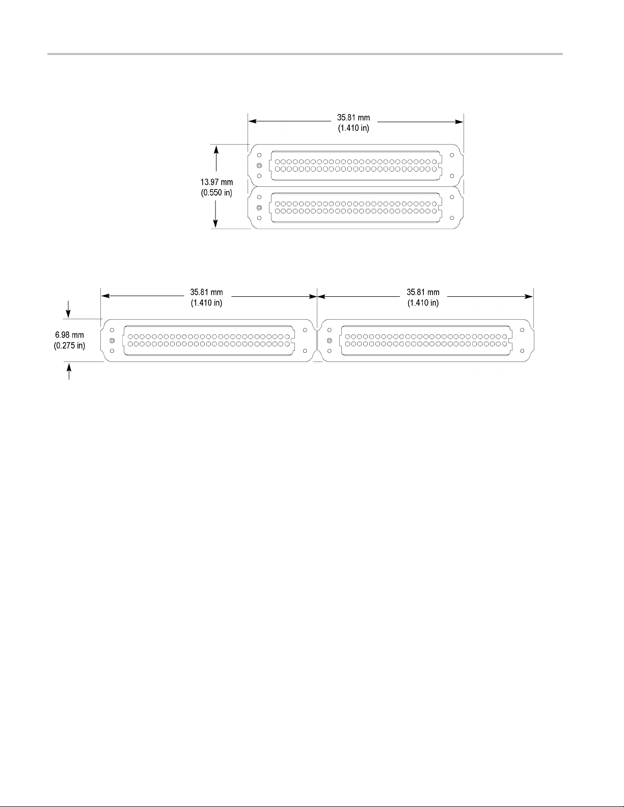
Probe Dimensions
The following figure shows the probe dimensions for the P6960DBL and
P6962DBL probes.
Figure 9: P6960DBL/P6962DBL probe dimensions
18 P6960DBL & P6962DBL High-Density Logic Analyzer Probes Instruction Manual

Reference
Probe Retention Assembly
Dimensions and K eepout
The probe reten
to help stabilize the probe. The following figure shows the dimensions of the
assembly.
All dimensions are per standard IPC tolerance, which is ±0.004 in.
CAUTION. To avoid solder creep, bend the assembly wires out after you insert the
wires in the board, and then solder the wires.
Figure 10: Retention assembly dimensions
The following figure shows the keepout area required for the retention assembly.
Vias must be placed outside of the keepout area. Any traces routed on the top
layer of the board must stay outside of the keepout area. Traces may be routed on
inner layers of the board through the keepout area.
tion assembly provides a housing around the connector footprint
Figure 11: Keepout area
P6960DBL & P6962DBL High-Density Logic Analyzer Probes Instruction Manual 19
Reference
Side-by-side and
End-to-end Layout
Dimensions
The following fi
Figure 12: Side-by-side layout
The following figure shows the dimensions for an end-to-end footprint layout.
gure shows the dimensions for side-by-side footprint layout.
Figure 13: End-to-end layout
Signal Routing
llowing figure shows examples of p ass-through s ignal routing for a
The fo
single-ended data configuration and a differential data configuration.
20 P6960DBL & P6962DBL High-Density Logic Analyzer Probes Instruction Manual

Figure 14: Signal routing on the target system
Reference
Mechanical
Considerations
Electrical Considerations
This sec
physical attachment requirements.
The PCB
signals when the signals routed around the holes have the corresponding return
current plane immediately below the signal trace for the entire signal path from
driver to receiver.
NOTE. For optimum signal integrity, there should be a continuous, uninterrupted
ground return plane along the entire signal path.
This section provides information on transmission lines and load models for the
P696xDBL Series Probes.
The low-frequency model is typically adequate for rise and fall times of 1 ns
or slower in a typical 25 Ω source impedance environment (50 Ω runs with a
pass-through connection). For source impedance outside this range, and/or rise
and fall times faster than 1 ns, use the high-frequency model to determine if a
significant difference is obtained in the modeling result.
The compression land pattern pad is not part of the load model. Make sure that
you include the compression land pad in the modeling.
tion provides information on compression footprint requirements and
holes, in general, do not have an impact upon the integrity of your
Transmission Lines. Due to the high performance nature of the interconnect,
ensure that stubs, which are greater than 1/4 length of the signal rise time, are
modeled as transmission lines.
P6960DBL & P6962DBL High-Density Logic Analyzer Probes Instruction Manual 21

Reference
P696x Series Pr
low-frequency and high-frequency model of the High-Density Single-Ended and
High-Density Differential Probes. (See Figure 15.) For the Differential Probes,
the load model is applied to both the + side and the – side of the signal.
Figure 15: High-Density probe load model
obes Load Model. The following electrical model includes a
The differential load for the clock inputs and probes can be modeled b y attaching
the single line model to each side (+ and –) of the differential signal. The + and
s of the differential signal are well insulated in the probe head up to and
–side
including the differential input stage.
22 P6960DBL & P6962DBL High-Density Logic Analyzer Probes Instruction Manual

Probe Footprint Dimensions
Use the probe footprint dimensions to lay out your circuit board pads and holes for
attaching the retention mechanism. (See Figure 16.) If you are using two retention
mechanisms, all dimensions remain the same as shown, except the overall length
and width. (See Figure 10 on page 19.) Supported pad finishes include immersion
gold, immer
All dimensions are per standard IPC tolerance, which is ±0.004 in.
Reference
sion silver, and hot air solder level.
NOTE. Tekt
performance.
Tektroni
unconnected to a ground plane. This prevents overheating the ground plane and
promotes quicker soldering of the retention posts to your PCB.
ronix recommends using immersion gold surface finish for best
x also recommends that the probe attachment holes float or remain
Figure 16: Probe footprint dimensions on the PCB
NOTE. You must maintain a solder mask web between the pads when traces are
routed between pads on the same layer. The solder mask must not encroach onto
the pads within the pad dimensions. (See Figure 11 on page 19.)
P6960DBL & P6962DBL High-Density Logic Analyzer Probes Instruction Manual 23

Reference
Other Design C
Via-in-pad
onsiderations
Traditional layout techniques require that vias are located next to a pad and that a
signal is routed to the pad, causing a stub and more PCB board area to be used for
the connecti
effects of the logic analyzer probing that you design into the circuit board.
Using viaminimize the stub length of the signals on your board, thus providing the smallest
intrusion to your signals. It also enables you to minimize the board area that
is used for the probe footprint and maintain the best electrical performance of
your design.
The following figure shows a footprint example where two pads use vias. Detail
A describes the recommended position of the via with respect to the pad.
All dimensions are per standard IPC tolerance, which is ±0.004 in.
on. Many new digital designs require you to minimize the electrical
in-pad to route signals to the pads on the circuit board allows you to
Figure 17: Optional Via-in-Pad placement recommendation
24 P6960DBL & P6962DBL High-Density Logic Analyzer Probes Instruction Manual

Reference
Probe Pinout D
efinition and Channel Assignment
This section contains probe pinout definitions and channel assignment tables for
the P696xDBL Series Probes.
P6960DBL High-Density
Probe
The following figure shows the pad assignments, pad numbers, and signal names
for the PCB footprint of the P6960DBL single-ended data, differential clock
logic analyzer probe. The P6960DBL probe has 32 data channels, one clock, and
one qualifier for each footprint. The P6960DBL probe double-probes signals on
the device under test.
Figure 18: P6960DBL single-ended PCB footprint pinout detail
The following table lists the channel mapping to a logic analyzer module for a
P6960DBL single-ended data, differential clock logic analyzer probe.
Table 2: Channel assignment for a P6960DBL single-ended data, differential clock logic analyzer probe
136 Channel
Pin number Signal name Probe 4 Probe 3 Probe 2 Probe 1
A1 D0 E2:0 A2:0 A0:0
A2 D1 E2:1 A2:1 A0:1
A3
A4 D4 E2:4 A2:4 A0:4
A5 D5 E2:5 A2:5 A0:5
A6
A7
A8
A9
A10 D10 E3:2 A3:2 A1:2
A11 D11 E3:3 A3:3 A1:3
A12
A13 D14 E3:6 A3:6 A1:6
A14 D15 E3:7 A3:7 A1:7
A15
A16 D18 E1:5 D3:5 D1:5
A17 D19 E1:4 D3:4 D1:4
A18
GND GND GND GND GND
GND GND GND GND GND
CK1+ Q3+ CK0+ CK1+ CK3+
CK1– Q3– CK0– CK1– CK3–
GND GND GND GND GND
GND GND GND GND GND
GND GND GND GND GND
GND GND GND GND GND
C2:0
C2:1
C2:4
C2:5
C3:2
C3:3
C3:6
C3:7
C1:5
C1:4
P6960DBL & P6962DBL High-Density Logic Analyzer Probes Instruction Manual 25

Reference
Table 2: Channel assignment for a P6960DBL single-ended data, differential clock logic analyzer probe (cont.)
136 Channel
Pin number Signal name Probe 4 Probe 3 Probe 2 Probe 1
A19 D22 E1:1 D3:1 D1:1
A20 D23 E1:0 D3:0 D1:0
A21
A22 D24 E0:7 D2:7 D0:7
A23 D25 E0:6 D2:6 D0:6
A24
A25 D28 E0:3 D2:3 D0:3
A26 D29 E0:2 D2:2 D0:2
A27
B1
B2 D2 E2:2 A2:2 A0:2
B3 D3 E2:3 A2:3 A0:3
B4
B5 D6 E2:6 A2:6 A0:6
B6 D7 E2:7 A2:7 A0:7
B7
B8 D8 E3:0 A3:0 A1:0
B9 D9 E3:1 A3:1 A1:1
B10
B11 D12 E3:4 A3:4 A1:4
B12 D13 E3:5 A3:5 A1:5
B13
B14 D16 E1:7 D3:7 D1:7
B15 D17 E1:6 D3:6 D1:6
B16
B17 D20 E1:3 D3:3 D1:3
B18 D21 E1:2 D3:2 D1:2
B19
B20
B21
B22
B23 D26 E0:5 D2:5 D0:5
B24 D27 E0:4 D2:4 D0:4
B25
B26 D30 E0:1 D2:1 D0:1
B27 D31 E0:0 D2:0 D0:0
GND GND GND GND GND
GND GND GND GND GND
GND GND GND GND GND
GND GND GND GND GND
GND GND GND GND GND
GND GND GND GND GND
GND GND GND GND GND
GND GND GND GND GND
GND GND GND GND GND
GND GND GND GND GND
CK2– Q2– Q0– CK2– Q1–
CK2+ Q2+ Q0+ CK2+ Q1+
GND GND GND GND GND
GND GND GND GND GND
C1:1
C1:0
C0:7
C0:6
C0:3
C0:2
C2:2
C2:3
C2:6
C2:7
C3:0
C3:1
C3:4
C3:5
C1:7
C1:6
C1:3
C1:2
C0:5
C0:4
C0:1
C0:0
26 P6960DBL & P6962DBL High-Density Logic Analyzer Probes Instruction Manual

Reference
P6962DBL High-Density
Probe
Figure 19: P6962DBL single-ended PCB footprint pinout detail
The P6962DBL pr
optimized to support 2X demultiplexing. This allows for full footprint utilization
when running the logic a nalyzer in half-channel mode.
The following figure shows the pad assignments, pad numbers, and signal names
for the PCB footprint of the P6962DBL single-ended data, differential clock
logic analyzer probe. The P6962DBL probe has 32 data channels and two clocks
for each footprint.
obe double-probes signals on the device under test and is
P6960DBL & P6962DBL High-Density Logic Analyzer Probes Instruction Manual 27

Reference
The following t
able lists the channel mapping to a logic analyzer module for a
P6962DBL single-ended data, differential clock logic analyzer probe.
Table 3: Channel assignment for a P6962DBL single-ended data, differential clock
logic analyzer probe
Pin number C and E group probe A0-A3 group probe
A1
A2
A3
A4
A5
A6
A7
A8
A9
A10
A11
A12
A13
A14
A15
A16 E3:5 A1:5
A17 E3:4 A1:4
A18
A19 E3:1 A1:1
A20 E3:0 A1:0
A21
A22 E2:7 A0:7
A23 E2:6 A0:6
A24
A25 E2:3 A0:3
A26 E2:2 A0:2
A27
B1
B2
B3
B4
B5
B6
B7
C2:0
C2:1
GND GND
C2:4
C2:5
GND GND
CK+ CK+
CK– CK–
GND GND
C3:2
C3:3
GND GND
C3:6
C3:7
GND GND
GND GND
GND GND
GND GND
GND GND
GND GND
C2:2
C2:3
GND GND
C2:6
C2:7
GND GND
A2:0
A2:1
A2:4
A2:5
A3:2
A3:3
A3:6
A3:7
A2:2
A2:3
A2:6
A2:7
28 P6960DBL & P6962DBL High-Density Logic Analyzer Probes Instruction Manual

logic analyze
Reference
Table 3: Channel assignment for a P6962DBL single-ended data, differential clock
r probe (cont.)
Pin number C and E group
B8
B9
B10
B11
B12
B13
B14 E3:7 A1:7
B15 E3:6 A1:6
B16
B17 E3:3 A1:3
B18 E3:2 A1:2
B19
B20
B21
B22
B23 E2:5 A0:5
4
B2
B25
B26 E2:1 A0:1
B27 E2:0 A0:0
C3:0
C3:1
GND GND
C3:4
C3:5
GND GND
GND GND
GND GND
CK– CK–
CK+ CK+
GND GND
:4
E2
ND
G
probe
A0-A3 g roup
A3:0
A3:1
A3:4
A3:5
A0
ND
G
probe
:4
P6960DBL & P6962DBL High-Density Logic Analyzer Probes Instruction Manual 29

Reference
30 P6960DBL & P6962DBL High-Density Logic Analyzer Probes Instruction Manual

Specifications
Mechanical an
d Electrical Specifications
The following table lists the mechanical and elec trical specifications for the
P696xDBL Series Probes. The electrical specifications apply when the probe is
connected b
Refer to the Tektronix Logic Analyz er Family Product Specifications document
(Tektroni
Family Product Documentation CD or downloadable from the Tektronix Web site
for a complete list of specifications, including overall system specifications.
Table 4: Mechanical and electrical specifications
Characteristic P6960DBL & P6962DBL
Threshold accuracy
Input resistance
Input capacitance 0.7 pF
Minimum digital signal swing 200 mV single-ended with TLA7BBx
Maximum nondestructive input signal to
probe
Delay from probe tip to module input
connector
Probe length
Operating range
etween a compatible logic analyzer and a target system.
x part number 071-1344-xx) available on the Tektronix Logic Analyzer
±(35 mV ±1% of setting)
11. 7 kΩ ±1%
±7.5 V
7.70 ns ±60 ps
1.8 m (6 ft)
+2.5 V to –1.25 V
TE. Because the length of the probes are electrically similar, they can be
NO
interchanged without problems.
P6960DBL & P6962DBL High-Density Logic Analyzer Probes Instruction Manual 31

Specifications
The following t
able shows the environmental specifications for the probes. The
probes are designed to meet Tektronix standard 062-2847-00 class 5.
Table 5: Environmental specifications
Characteristic P69xx
Temperature
Operating
Nonoperati
Humidity
Altitude
Operating
Nonoper
Electrostatic immunity 6 kV
ng
ating
0 °C to +50 °C (0 °F to +122 °F)
-51 °C to +71
10 °C to 30 °C
relative humidity
30 °C to 40 °C (+86 °F to + 104 °F) 75%
relative h
40 °C to 50 °C (+104 °F to +122 °F) 45%
relative humidity
9843 ft (3,000 m)
40,000 f
°C (-60 °F to +160 °F)
(+50 °F to +86 °F) 95%
umidity
t (12,192 m)
32 P6960DBL & P6962DBL High-Density Logic Analyzer Probes Instruction Manual

Maintenance
The P696xDBL Series High-Density Logic Analyzer Probes do not require
scheduled or periodic maintenance. Refer to the Functional Check section below
to verify the basic functionality of the probes.
Probe Calib
ration
To confirm that the probes meet or exceed the performance requirements for
published specifications with a compatible logic analyzer module, you must return
the probes
Functional Check
Connect t
verify that the acquired data is displayed in either the listing or waveform
windows.
Inspection and Cleaning
CAUTION. To prevent damage during the probe connection process, do not touch
the ex
edge or corner.
To ma
contaminants. Remove dirt and dust with a soft brush. Avoid brushing or rubbing
the c-spring contacts. For more extensive cleaning, use only a damp cloth. Never
use abrasive cleaners or organic solvents.
to your local Tektronix service center.
he logic analyzer probes to a signal source, start an acquisition, and
posed edge of the interface clip. Do not drag the contacts against a hard
intain a reliable electrical contact, keep the probes free of dirt, dust, and
P6960DBL & P6962DBL High-Density Logic Analyzer Probes Instruction Manual 33

Maintenance
Service Strat
egy
Replacing the cLGA Clip
The P696xDBL Series Probes use replaceable c-spring cLGA clips. (See the
replacement procedure below.) If a probe failure other than the cLGA clip occurs,
return the en
For replacement part number information, refer to the Replaceable Parts List.
(See page 38, Using the Replaceable Parts List.)
1. Gently pull one side of the clip away from the probe head, as shown in
following figure, and then remove the entire clip.
2. Align the new clip with the probe head and gently snap it into place.
3. Test the probe to confirm that all channels are functional.
tire probe to your Tektronix service center for repair.
Figure 20: Replacing the cLGA clip
34 P6960DBL & P6962DBL High-Density Logic Analyzer Probes Instruction Manual

Repackaging Instructions
Use the original packaging, if possible, to return or store the probes. If the
original packaging is not available, use a corrugated cardboard shipping carton.
Add cushioning material to prevent the probes from moving inside the shipping
container.
Enclose the following information when shipping the probe to a Tektronix Service
Center.
Maintenance
Owner’s address
Name and phone number of a contact person
Type of probe
Reason for return
Full des
cription of the service required
P6960DBL & P6962DBL High-Density Logic Analyzer Probes Instruction Manual 35

Maintenance
36 P6960DBL & P6962DBL High-Density Logic Analyzer Probes Instruction Manual

Replaceable Parts
This chapter contains a list of the replaceable components for the P696xDBL
Series Probes. Use this list to identify and order replacement parts.
Parts Ordering Information
Replacement parts are available through your local Tektronix field office or
representative.
Changes to Tektronix products are sometimes made to accommodate improved
components as they become available and to give you the benefit of the latest
improvements. Therefore, when ordering parts, it is important to include the
followin
If you order a part that has been replaced with a different or improved part, your
local Tektronix field office or representative will contact you concerning any
change in part number.
ginformationinyourorder.
Part number
Instrument type or model number
Instrument serial number
Instrument modification number, if applicable
P6960DBL & P6962DBL High-Density Logic Analyzer Probes Instruction Manual 37

Replaceable Parts
Using the Replaceable Parts List
Replaceable Parts
The P696xDBL Series Probes contain only the cLGA clip as a replaceable
part. If probe failure occurs, return the entire probe to your Tektronix service
representative for repair.
Refer to the following list for replaceable items:
Table 6: Parts list column descriptions
Column Column nam
1
2 Tektroni
3 and 4
5
6
Figure & in
Serial number Column three indicates the serial number at which the part was first
Qty This indicates the quantity of parts used.
Name & description An item name is separated from the description by a colon (:).
e
dex number
x part number
Descripti
Items in th
exploded view illustrations that follow.
Use this part number when ordering replacement parts from Tektronix.
effective. Column four indicates the serial number at which the part
was disc
numbers.
Because of space limitations, an item name may sometimes appear as
incom
item name identification.
on
is section reference figure and index numbers to the
ontinued. No entries indicate that the part is good for all serial
plete. Use the U.S. Federal Catalog handbook H6-1 for further
Abbreviations
Abbreviations conform to American National Standard ANSI Y1.1-1972.
38 P6960DBL & P6962DBL High-Density Logic Analyzer Probes Instruction Manual

Replaceable Parts
Table 7: P6960D
Figure
&index
number
21--1 010-0779-10 1
-2 020-2622-XX 1
-3 200-4893-XX 1
BL replaceable parts list
Tektronix
part
number
020-2908-XX 1
346-0300-XX 1
003-189
071-24
335-1955-XX 1
0-XX
55-XX
Serial
no.
effective
Serial no.
discont’d Qty Name & descrip
P6960DBL STA
NDARD ACCESSORIES
tion
P6960DBL PR
COMPONENT K
PREINSTALLED ON THE PROBE; 1 E A, P69XX SERIES
PROBE, SAFETY CONTROLLED
COVER,PROTECTIVE; BLACK VINYL (PLASTISOL) WITH
STATIC-D
P69xx PRO
STRAP, V
QTY 2 BAGGED & LABELED
1
1
TOOL,HAND; USED TO TIGHTEN PROBE HEAD TO DUT
MANUAL,TECH; QUADFOLD, INSTALLATION/LABELING
INSTRUCTIONS FOR P6960DBL
P6960DBL PROBE, SHEET OF LABELS
OBE (INCLUDES SHEET OF LABELS)
IT, CLGA INTERFACE CLIP
ISSIPATIVE ADDITIVE
BE RETENTION ASSEMBLY KIT, QTY 2
ELCRO; ONE WRAP, BLACK, 0.500W X 8.00L,
Figure 21: P6960DBL High-Density probe accessories
P6960DBL & P6962DBL High-Density Logic Analyzer Probes Instruction Manual 39

Replaceable Parts
Table 8: P6962D
Figure
&index
number
22--1 010-0780-10 1
-2 020-2622-XX 1
-3 200-4893-XX 1
BL replaceable parts list
Tektronix
part
number
020-2908-XX 1
346-0300-XX 1
0-XX
003-189
071-2456-XX 1
335-1956-XX 1
Serial
no.
effective
Serial no.
discont’d Qty Name & descrip
P6962DBL STA
NDARD ACCESSORIES
tion
P6962DBL PR
COMPONENT K
PREINSTALLED ON THE PROBE; 1 EA, P69XX
SERIES PROBE, SAFETY CONTROLLED
COVER,PROTECTIVE; BLACK VINYL (PLASTISOL)
WITH STAT
P69xx PRO
STRAP,V
8.00L, QTY 2 BAGGED & LABELED
1
TOOL,HAND; USED TO TIGHTE N PROBE HEAD
TO DUT
MANUAL, TECH; QUADFOLD, INSTALLATION/
LABELI
P6962
OBE (INCLUDES SHEET OF LABELS)
IT, CLGA INTERFACE CLIP
IC-DISSIPATIVE ADDITIVE
BE RETENTION ASSEMBLY KIT, QTY 2
ELCRO; ONE WRAP, BLACK, 0.500W X
NG INSTRUCTIONS FOR P6962DBL
DBL PROBE, SHEET OF LABELS
Figure 22: P6962DBL High-Density probe accessories
40 P6960DBL & P6962DBL High-Density Logic Analyzer Probes Instruction Manual

Replaceable Parts
Table 9: P696xD
Figure &
index number
23--1 020-2908-00 1
-2 020-2910-00 1
BLSeries Probes optional accessories
Tektronix
part
number
Serial no.
effective
P696xDBL SERIES PROBES OPTIONAL ACCESSORIES
Serial no.
discont’d Qty Name & description
Figure 23: Optional accessories
P69xx PROBE RETENTION
ASSEMBLY KI
P69xx PROBE
ASSEMBLY KIT, QTY 50
T, QTY 2
RETENTION
P6960DBL & P6962DBL High-Density Logic Analyzer Probes Instruction Manual 41

Replaceable Parts
42 P6960DBL & P6962DBL High-Density Logic Analyzer Probes Instruction Manual

Index
A
Adapters
definition of
Attaching Probe Labels, 1
, viii
C
Calibration
probe, 33
Cleaning
compression footprints, 7
inspecti
cLGA, vi
cLGA Interface Clip
handling, 9
replacing, 34
Clocking
Sourc
Clocks, 15
Commonly used terms, vi
Compression footprint, vi, 7
Connecting
probes to logic analyzer, 6
pro
on and, 33
e Synchronous, 17
bes to target system, 7
D
Designing an interface, 15
electrical considerations, 21
mechanical
considerations, 21
Differential input amplitude
definition, vi
Documentation
related, v
F
Flying Lead Set, vi
Functional c
heck, vii, 33
H
High Density Probe,
P6960DBL, 2
High Density Probe,
P6962DBL, 4
I
Inspection and cleaning, 33
K
Keepou
t area, vii, 19
L
Load model
P696x Series Probes, 21
Logic analyzer
connecting probes, 6
M
Maintenance, 33
ctional check, 33
fun
inspection and cleaning, 33
probe calibration, 33
repackaging instructions, 35
service strategy, 34
Mechanical specifications, 31
erged module, 17
M
Module, vii
Parts
ordering information, 37
using the replaceable parts
list, 38
PCB (printe
Probe
Troubleshooting DUT
Probe Heads
Handling the interface clips, 9
Probes
adapter, definition of, viii
calibration, 33
cleaning the compression
connecting probes to the logic
connecting probes to the target
definition of, vii
footprint dimensions, 23
head, definition of, viii
lab
P6960DBL High Density
P6962DBL High Density
product description, 1
eturning, 35
r
storing, 35
Probing analog signals, 17
d circuit board), vii
connections, 11
footprints, 7
zer, 6
analy
system, 7
els, 1
Probe, 2
Probe, 4
Q
Qualifiers, 15
E
Electrical considerations
P696x Series Probes load
model, 21
Transmission lines, 21
Electrical specifications, 31
P6960DBL & P6962DBL High-Density Logic Analyzer Probes Instruction Manual 43
O
Ordering parts information, 37
P
P6960DBL pinout, 25
P6962DBL pinout, 27
R
Range recognition, 17
Related documentation, v
Repackaging instructions, 35
Replacing the cLGA interface
clip, 34
Retention assembly, 8, 19
Returning probes, 35

Index
S
Service strategy, 34
Signal conne
Signal fixturing, 15
SMT KlipChip, viii
Specifications
electrical, 31
mechanical, 31
ctions, 15
Storing probes
, 13, 35
T
Target system
connecting probes, 7
Terms
commonly used, vi
Transmission Lines, 21
Troubleshooti
Probe DUT connections, 11
ng
44 P6960DBL & P6962DBL High-Density Logic Analyzer Probes Instruction Manual
 Loading...