

Page 1

Instruction Manual
P68XX Series
Logic Analyzer Probes
071-1059-04
There are no current European directives that apply to this product. This product provides cable
and test lead connections to a test object of electronic measuring and test equipment.
Warning
The servicing instructions are for use by qualified
personnel only. To avoid personal injury, do not
perform any servicing unless you are qualified to
do so. Refer to all safety summaries prior to
performing service.
www.tektronix.com
Page 2

Copyright © Tektronix, Inc. All rights reserved.
Tektronix products are covered by U.S. and foreign patents, issued and pending. Information in this publication supercedes
that in all previously published material . Specifica tions and price change privileges reserved.
Tektronix, Inc., P.O. Box 500, Beaverton, OR 97077
TEKTRONIX and TEK are registered trademarks of Tektronix, Inc.
MagniVu, iView, PatGenVu, PowerFlex, QuickStart, and TLAVu are unregistered trademarks of Tektronix, Inc.
Page 3

WARRANTY
Tektronix warrants that the products that it manufactures and sells will be free from defects in materials and
workmanship for a period of one (1) year from the dat e of shipment. If a product proves defective during this
warranty period, Tektronix, at its option, either will repair the defective product without charge for parts and labor,
or will provide a replacement in exchange for the defective product.
In order to obtain service under this warranty, Customer must notify Tektronix of the defect before the expiration
of the warranty period and make suitable arrangements for the performance of service. Customer shall be
responsible for packaging and shipping the defective product to the service center designated by Tektronix, with
shipping charges prepaid. Tektronix shall pay for the return of the product to Customer if the shipment is to a
location within the country in which the Tektronix service ce nter is located. Customer shall be responsible for
paying all shipping charges, duties, taxes, and any other charges for produc ts returned to any other locations.
This warranty shall not apply to any defect, failure or damage caused by improper use or im proper or inadequate
maintenance and care. Tektronix shall not be obligated to furnish service under this warranty a) to repair dama ge
resulting from attempts by personnel other than Tektronix representatives to install, re pair or service the product;
b) to repair damage resulting from improper use or conne ction to incompatible equipment; c) to repair any
damage or malfunction caused by the use of non-Tektronix supplies; or d) to service a product that has been
modified or integrated with other products when the effect of such modification or integration increases the time
or difficulty of servicing the product.
THIS W ARRANTY IS GIVEN BY TEKTRONIX IN LIEU OF ANY OTHER WARRANTIES, EXPRESS
OR IMPLIED. TEKTRONIX AND ITS VENDORS DISCLAIM ANY IMPLIED WARRANTIES OF
MERCHANTABILITY OR FITNESS FOR A PARTICULAR PURPOSE. TEKTRONIX’
RESPONSIBILITY TO REPAIR OR REPLACE DEFECTIVE PRODUCTS IS THE SOLE AND
EXCLUSIVE REMEDY PROVIDED TO THE CUSTOMER FOR BREACH OF THIS WARRANTY.
TEKTRONIX AND ITS VENDORS WILL NOT BE LIABLE FOR ANY INDIRECT, SPECIAL,
INCIDENTAL, OR CONSEQUENTIAL DAMAGES IRRESPECTIVE OF WHETHER TEKTRONIX OR
THE VENDOR HAS ADVANCE NOTICE OF THE POSSIBILITY OF SUCH DAMAGES.
Page 4

Page 5

Table of Contents
Operating Basics
General Safety Summary vii...................................
Preface ix...................................................
Related Documentation ix...........................................
CommonlyUsedTerms x...........................................
Contacting Tektronix xiii.............................................
Product Description 1--1........................................
P6810 General Purpose Probe 1--2......................................
P6810 Leadset Adapters and Accessories 1--3.............................
P6860 High-Density Probe 1--5.........................................
P6864 High-Density 4X Probe 1--6......................................
P6880 High-Density Differential Probe 1--8...............................
Mictor-on-PCB to P6860 Compression Adapter 1--9........................
Compression-on-PCB to P6434 Mictor Adapter 1--10........................
Attaching Probe Labels 1--12.....................................
Connecting the Probes to the Logic Analyzer 1--13...................
Cleaning the P686x and P6880 Compression Footprints 1--14.........
Cleaning the P686x and P6880 Probe Heads 1--14...................
Storing the P686x and P6880 Probe Heads 1--15.....................
Connecting the Probes to the Target System 1--16....................
Connecting the P6810 General Purpose Probe 1--16.........................
Connecting the P686x High Density and P6880 Differential Probes 1--18........
Installing the Correct Elastomer Holder 1--18..............................
Connecting the Mictor-on-PCB to P6860 Compression Adapter
(Applies to P6860 Probe Only) 1--21..................................
Connecting the Compression-on-PCB to P6434 Mictor Adapter 1--21...........
Reference
Designing an Interface Between the P68xx Probes and a
T arget System 2--1.........................................
Signal Fixturing Considerations 2--1.....................................
Signal Names 2--6...................................................
Land Footprints 2--22..................................................
Mechanical Considerations 2 --27........................................
Physical Attachment Requirements for the P6810 Probe 2--31.................
Physical Attachment Requirements for the P686x and P6880 Probes 2--31.......
Physical Attachment Requirements for the Compression-on-PCB to P6434
Mictor and Mictor-on-PCB to P6860 Compression Adapters 2--33..........
Electrical Considerations 2--33..........................................
Transmission Lines 2--34...............................................
P6810 General Purpose Probe Load Model 2--34............................
P686x High-Density and P6880 High-Density Differential Probes
Load Model 2--36.................................................
P68XX Series Logic Analyzer Probes Instruction Manual
i
Page 6

Table of Contents
Specifications
Maintenance
Replaceable Parts
Index
Mechanical and Electrical Specifications 3--1......................
Probe Calibration 4--1.........................................
Service Strategy 4--1...........................................
Functional Check 4--1..........................................
Inspection and Cleaning 4--2....................................
Repackaging Instructions 4--2...................................
Parts Ordering Information 5--1.................................
Using the Replaceable Parts List 5--1.............................
Mfr. Code to Manufacturer Cross Index 5--2..............................
ii
P68XX Series Logic Analyzer Probes Instruction Manual
Page 7

List of Figures
Table of Contents
Figure i: Differential input amplitude x.........................
Figure ii: Probe example xi....................................
Figure 1--1: P6810 General Purpose probe 1--2.....................
Figure 1--2: P6810 probe leadset adapters and accessories 1--4........
Figure 1--3: P6860 High-Density probe 1--5........................
Figure 1--4: P6864 High-Density 4X probe 1--6.....................
Figure 1--5: P6880 High-Density Differential probe 1--8..............
Figure 1--6: Mictor-on-PCB to P6860 Compression adapter 1--10.......
Figure 1--7: 34-Channel Compression-on-PCB to P6434 Mictor
adapter 1--11...............................................
Figure 1--8: Clearance for probe connection using
Compression-on-PCB to P6434 Mictor adapter 1--12..............
Figure 1--9: Connecting the probes to the logic analyzer 1--13..........
Figure 1--10: Cleaning the probe heads 1--15........................
Figure 1--11: Storing the probe heads 1--16.........................
Figure 1--12: Connecting the P6810 probe to the target system 1--17....
Figure 1--13: Press-in Nuts installation 1--18........................
Figure 1--14: Connecting the P686x and P6880 probes to the
target system 1--20..........................................
Figure 2--1: P6810 General-Purpose probe land footprint 2--23........
Figure 2--2: P686x High-Density probe land footprint 2--24............
Figure 2 --3: High-Density probe land footprint in a typical
pass-through signal path layout configuration 2--25..............
Figure 2--4: Example layouts of the High-Density compression
compared to the mictor land footprints 2--25....................
Figure 2--5: P6880 Differential probe land footprint 2--26.............
Figure 2 --6: High-Density Differential probe land footprint in a
typical pass-through signal path layout configuration 2--27........
Figure 2--7: Land footprint requirements for the P686x and P6880
probes (top view) 2--28.......................................
Figure 2 --8: Land footprint requirements for the 34 channel
Compression-on-PCB to P6434 Mictor adapter 2-- 30.............
Figure 2 --9: Land footprint requirements for the 17 channel
Compression-on-PCB to P6434 Mictor adapter 2--30..............
P68XX Series Logic Analyzer Probes Instruction Manual
iii
Page 8

Table of Contents
Figure 2--10: Physical attachment requirements for the
P6810 probe 2--31...........................................
Figure 2--11: Nut Bar design 2--32.................................
Figure 2--12: Press-in Nut design 2--33.............................
Figure 2 --13: Single podlet load model 2--34.........................
Figure 2--14: Eight-channel leadset (barrel connectors) 2--35..........
Figure 2--15: One-channel leadset (barrel connector) 2--35............
Figure 2 --16: Eight-channel differential leadset 2--35.................
Figure 2 --17: High-Density and High-Density Differential probe
load model 2--36............................................
Figure 2--18: Mictor-on-PCB to Compression adapter load model 2--37.
Figure 2--19: Compression-on-PCB to P6434 Mictor adapter
load model 2--37............................................
Figure 5--1: P6810 General Purpose probe accessories 5--3...........
Figure 5--2: P6860 High-Density probe accessories 5--4..............
Figure 5--3: P6864 High-Density 4X probe accessories 5--5...........
Figure 5--4: P6880 High-Density Differential probe accessories 5--6....
Figure 5--5: Optional accessories 5--7.............................
iv
P68XX Series Logic Analyzer Probes Instruction Manual
Page 9

List of Tables
Table of Contents
Table 2--1: Logic analyzer clock and qualifier availability 2--2........
T able 2--2: 2X Demultiplexing source-to-destination
channel assignments 2--4....................................
T able 2--3: 4X Demultiplexing source-to-destination
channel assignments 2--5....................................
Table 2--4: P6810 Probe signal connections on 136 and
102 channel modules for probe #4 and probe #3 2--7.............
Table 2--5: P6810 Probe signal connections on 102 and
136 channel modules for probe #2 and probe #1 2--8.............
Table 2--6: P6810 Probe signal connections on 68 and
34 channel modules 2--9.....................................
Table 2--7: P6860 High-Density Probe channel mapping on
136 and 102 channel modules 2--10...........................
Table 2--8: P6860 High-Density Probe channel mapping on
68 and 34 channel modules 2--11.............................
Table 2--9: P6864 High-Density 4X Probe channel mapping on
34, 68, 102 and 136 channel mod ules 2 --12......................
Table 2--10: P6880 High-Density Differential Probe channel mapping
on 136 and 102 channel modules for probe #4 and probe #3 2--13..
Table 2--11: P6880 High-Density Differential Probe channel mapping
on 136 and 102 channel modules for probe #2 and probe #1 2--14..
Table 2--12: P6880 High-Density Differential Probe channel mapping
on 68 and 34 channel modules 2--15...........................
Table 2--13: Recommended Compression-on-PCB to P6434 Mictor
adapter and Mictor-on-PCB to Compression adapter channel
mapping for 136 and 102 channel modules 2--16.................
Table 2--14: Recommended Compression-on-PCB to P6434 Mictor
adapter and Mictor-on-PCB to Compression adapter channel
mapping for 68 channel module 2--18..........................
Table 2--15: Recommended Compression-on-PCB to P6434 Mictor
adapter and Mictor-on-PCB to Compression adapter channel
mapping for 34 channel module 2--20..........................
Table 2--16: Characteristics 2--34.................................
T able 3--1: Electrical and mechanical specifications 3--1.............
T able 3--2: Environmental specifications 3--2......................
P68XX Series Logic Analyzer Probes Instruction Manual
v
Page 10

Table of Contents
vi
P68XX Series Logic Analyzer Probes Instruction Manual
Page 11

General Safety Summary
Review the following safety precautions to avoid injury and prevent damage to
this product or any products connected to it. To avoid potential hazards, use this
product only as specified.
Only qualified personnel should perform service procedures.
While using this product, you may need to access other parts of the system. Read
the General Safety Summary in other system manuals for warnings and cautions
related to operating the system.
ToAvoidFireor
Personal Injury
Connect and Disconnect Properly. Connect the probe output to the measurement
instrument before connecting the probe to the circuit under test. Disconnect the
probe input and the probe ground from the circuit under test before disconnecting
the probe from the measurement instrument.
Observe All Terminal Ratings. To avoid fire or shock hazard, observe all ratings
and markings on the product. Consult the product manual for further ratings
information before making connections to the product.
Do not apply a potential to any terminal, including the common terminal, that
exceeds the maximum rating of that terminal.
Avoid Exposed Circuitry. Do not touch exposed connections and components
when power is present.
Do Not Operate With Suspected Failures. If you suspect there is damage to this
product, have it inspected by qualified service personnel.
Do Not Operate in Wet/Damp Conditions.
Do Not Operate in an Explosive Atmosphere.
Keep Product Surfaces Clean and Dry.
Provide Proper Ventilation. Refer to the manual’s instructions for details on
installing the product so it has proper ventilation.
P68XX Series Logic Analyzer Probes Instruction Manual
vii
Page 12
General Safety Summary
Symbols and Terms
Terms in this Manual. These terms may appear in this manual:
WARNING. Warning statements identify conditions or practices that could result
in injury or loss of life.
CAUTION. Caution statements identify conditions or practices that could result in
damage to this product or other property.
Terms on the Product. These terms may appear on the product:
DANGER indicates an injury hazard immediately accessible as you read the
marking.
WARNING indicates an injury hazard not immediately accessible as you read the
marking.
CAUTION indicates a hazard to property including the product.
Symbols on the Product. The following symbols may appear on the product:
CAUTION
Refer to Manual
viii
P68XX Series Logic Analyzer Probes Instruction Manual
Page 13

Preface
Related Documentation
This document provides information on using and servicing the P68xx series
logic analyzer probes.
In addition to these probe instructions, the following documentation is available
for your Tektronix 700 Series Logic Analyzers.
H The Tektronix Logic Analyzer Family User Manual provides overall user
information for the TLA Series Logic Analyzer.
H The TLA700 Series Logic Analyzer Installation Manual provides installation
information for the TLA700 Series Logic Analyzer.
H The TLA5000 Series Logic Analyzer Installation Manual provides installa-
tion information for the TLA5000 Series Logic Analyzer.
H The TLA7Axx Module Service Manual that provides module-level service
information for major components of the TLA Series Logic Analyzer.
H P6810 General Purpose Logic Analyzer Probe Label Instructions
H P6860 High Density Logic Analyzer Probe Label Instructions
H P6864 High Density 4X Logic Analyzer Probe Label Instructions
H P6880 High Density Differential Logic Analyzer Probe Label Instructions
H The online help provides information about the user interface, the TLA700
Programmatic Interface (TPI), and the TLAScript interface. To view the
online help, select Help Topics from the Help menu. The TLAScript online
help provides links to related topics in TPI.
H The online release notes provide last-minute product and software informa-
tion not included in this manual. To access the Probe Manual Release Notes,
click Start > Programs > Tektronix Logic Analyzer > TLA Release Notes.
H A series of microprocessor support instruction manuals provide operating
and service instructions for the individual microprocessor support packages.
H The TLA7QS QuickStart Training Manual provides training exercises to help
you learn key features of the logic analyzer. The training manual is designed
to be used with the TLA7QS QuickStart training board.
H The P6434 Mass Termination Probe Instructions provides instructions for
using the P6434 Probes with older Tektronix logic analyzers.
P68XX Series Logic Analyzer Probes Instruction Manual
ix
Page 14
Preface
Commonly Used Terms
H The P6417 & P6418 Logic Analyzer Probes Instructions provides instruc-
tions for using the P6417 and P6418 Probes.
H The P6419 Logic Analyzer Probe Instructions provides instructions for using
P6419 Probes.
Refer to the following list of commonly used terms throughout the manual.
Compression Footprint
Differential Input
Amplitude Definition
A connectorless, solderless contact between your PCB and the P6860 and P6880
Probes. Connection is obtained by applying pressure between your PCB and the
probe through a Z-axis elastomer.
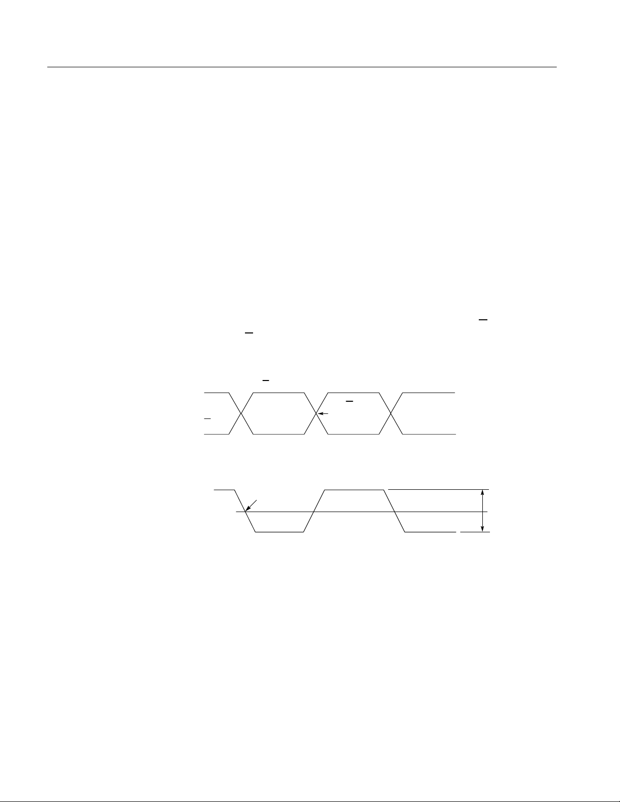
For differential signals, the magnitude of the difference voltage V
(and Vmin-V
V
V
Differential equivalent signal input (300 mV swing) as viewed by the logic analyzer and the
analog probe output**.
*
V
TH = OV
* Note: For differential inputs, the module threshold should be set to OV (assuming no
common mode error).
** Note: See online help for further analog output details.
max) must be greater than or equal to 150 mV. Refer to Figure i.
Differential input (150 mV minimum swing each side, --2.5 V maximum)
Vmax
V=V
OV Difference
Vmin
OV Difference
max-Vmin
1.15 V
1V
150 mV
OV
--150 mV
Figure i: Differential input amplitude
Functional Check
Procedure
Keepout Area
Functional check procedures verify the basic functionality of the probes by
confirming that the probes recognize signal activity at the probe tips.
The area of the printed circuit board in which only probe components may be
mounted.
x
P68XX Series Logic Analyzer Probes Instruction Manual
Page 15
Preface
Module
Module End
PCB
Podlet
Podlet Holder
Probe
The unit that plugs into a mainframe which provides instrument capabilities such
as logic analysis.
The end of the probe which plugs into the module unit.
An acronym for Printed Circuit Board; also known as Etched Circuit Board
(ECB).
A circuit contained in a flex lead and attached to a probe which provides
square-pin connections to the circuit under test for one data acquisition channel
and a reference pin.
A removable clip that groups eight individual podlets into a single 8-wide P6810
Probeassembly.Thisprovideseasewhenconnectingtoarowof2x82.54mm
(0.100 in) square pins.
The device that connects a module with a target system.
Figure ii: Probe example
Probe Adapter
P68XX Series Logic Analyzer Probes Instruction Manual
A device that connects the LA module probe to a target system.
Module end
Way station
Probe head
xi
Page 16

Preface
Probe Head
SMT KlipChip
Way Station
Z-axis eLastomer
The end of the probe (see Figure ii) that connects to the target system or probe
adapter.
An interface device for attaching logic analyzer probes to components with a
maximum lead diameter of 2.413 mm (0.095 in) and a stackable on lead centers
of 1.27 mm (0.050 in).
An intermediate probe part (see Figure ii) used to connect the heads of the P6810
and P6880 Probes to a single ribbon cable.
Silicone-based material containing vertical wires that conduct only in the z-axis.
xii
P68XX Series Logic Analyzer Probes Instruction Manual
Page 17

Contacting Tektronix
Preface
Phone 1-800-833-9200*
Address Tektronix, Inc.
Department or name (if known)
14200 SW Karl Braun Drive
P.O. Box 500
Beaverton, OR 97077
USA
Web site www.tektronix.com
Sales support 1-800-833-9200, select option 1*
Service support 1-800-833-9200, select option 2*
Technical support Email: techsupport@tektronix.com
1-800-833-9200, select option 3*
6:00 a.m. -- 5:00 p.m. Pacific time
* This phone number is toll free in North America. After office hours, please leave a
voice mail message.
Outside North America, contact a Tektronix sales office or distributor; see the
Tektronix web site for a list of offices.
P68XX Series Logic Analyzer Probes Instruction Manual
xiii
Page 18

Preface
xiv
P68XX Series Logic Analyzer Probes Instruction Manual
Page 19

Operating Basics
Page 20

Page 21

Operating Basics
Product Description
This section provides a brief description of the Tektronix P68xx Logic Analyzer
Probes and adapters, information on attaching color-coded probe labels, and
probe and adapter connection instructions from the logic analyzer to the target
system.
The P68xx Logic Analyzer Probes connect a TLA7Axx Series Logic Analyzer
module to a target system. The P6810, P6860 and P6880 probes consists of
34 channels, while the P6864 probe consists of 17 channels. You can connect the
P6810 probe to the target system through podlet holders or leadsets. In addition,
a variety of leadsets, SMT KlipChips and adapters aid in your connection to the
target system. The P6860 probe can be connected through the use of the
compression land pattern or a Mictor connector using the Mictor-on-PCB to
P6434 to Compression adapter. The P6880 probe is designed for connection to
the compression land pattern only configured for differential signals. The P6880
is not compatible with either the Mictor-on-PCB to P6860 probe adapter or the
Compression-on-PCB to P6434 probe adapter. The P6864 probe can be
connected through the use of the compression land pattern. Note that the P6864
is designed to minimize the needed area on the circuit board for connections
when using the 4X clocking mode in the logic analyzer module.
P68XX Series Logic Analyzer Probes Instruction Manual
1- 1
Page 22
Operating Basics
P6810 General Purpose
Probe
The P6810 Probe is a 34-channel, general purpose probe (see Figure 1--1).
34 Channel probe to
TLA7Axx module
Ground lead
Way stations
1--Channel podlet
(clock/qual)
8--Channel podlet
group (data)
Figure 1- 1: P6810 General Purpose pr obe
NOTE. Remember to connect the ground lead of the way station to the target
system to improve signal integrity.
The following list details the capabilities and qualities of the P6810 Probe:
H 34 individual active channel podlets
H Differential and single-ended data, clock and qualification inputs
H 2 mm (0.079 in) and 2.54 mm (0.1 in) podlet and leadset connection
capability
H Maximum non-destructive input voltage
H Leadset support for both single-ended and differential applications
H Podlet holder for 8-channel applications
H Color-coded signal connectors
H --2.5 V to +5 V input operating range
1- 2
P68XX Series Logic Analyzer Probes Instruction Manual
Page 23

Operating Basics
H --2.0 V to +4.5 V threshold range
H 300 mV minimum single-ended signal amplitude
H 150 mV amplitude each side minimum differential signal
H Minimal loading of <1 pFand20kΩ to ground
H Operation in normal or inverted polarity is acceptable
H Any common mode voltage is acceptable so long as the maximum positive
voltage does not exceed +5 V and the maximum negative voltage does not
exceed --2.5 V
NOTE. Single podlet input capacitance is 0.7 pF, but in a group, each podlet will
have 1 pF input capacitance.
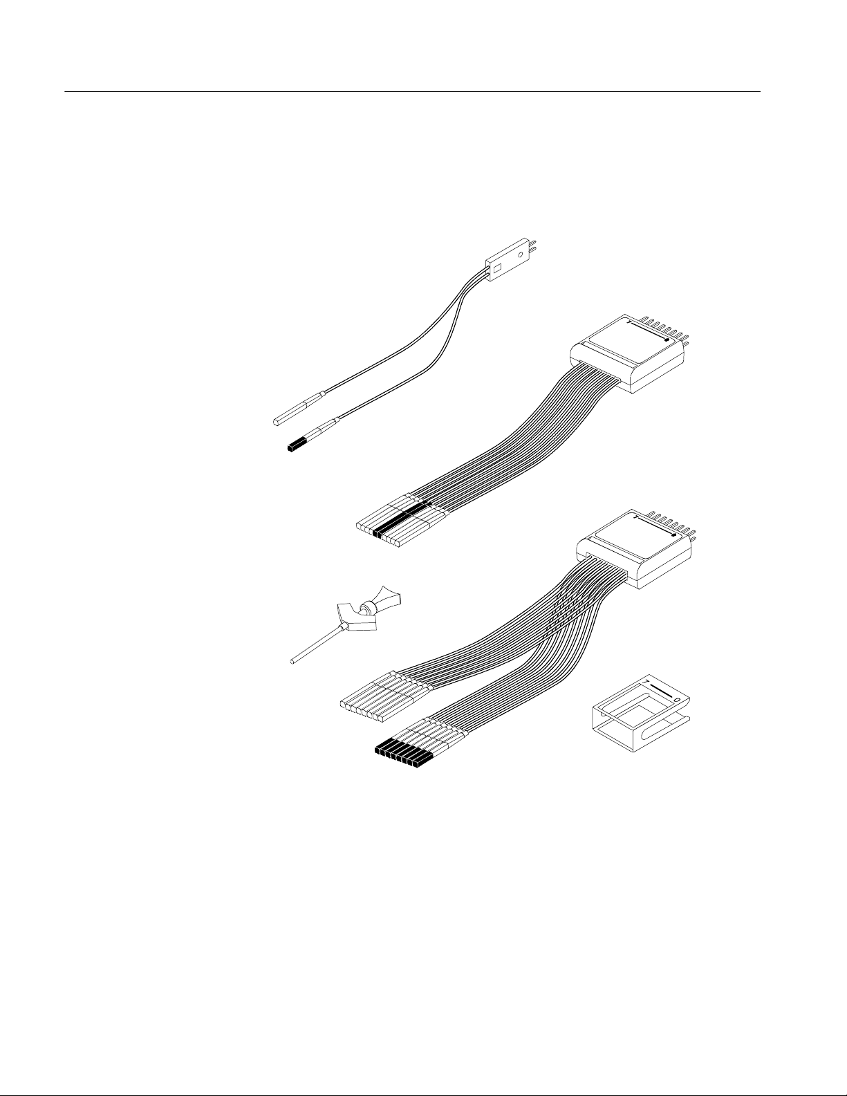
P6810 Leadset Adapters
and Accessories
Leadsets enhance flexible access to the target system signals by allowing
single-pin podlet connections of signals and grounds. This allows the separation
of ground and signal connections, providing flexible access to the PCB and
backplane connections where signals are not easily accessible together. The
following leadsets and accessories accompany the P6810 General Purpose Probe.
H 1-Channel single-ended and differential leadset. Supports individual
leadset connections to backplanes and other connection points requiring
single-ended 2 mm (0.079 in) and 2.54 mm (0.1 in) connections. Both leads
contain 150 Ω damping resistors in the lead tips.
H 8-Channel single-ended leadset. Supports individual leadset connections to
backplanes and other multiple, dense, single-end connections in a 2 mm
(0.079 in) and/or 2.54 mm (0.1 in) pin array. Two common ground connec-
tions for all input signals. The positive leads contain 150 Ω damping
resistors and the leadset housing contains a 150 Ω damping resistor in the
ground path of each channel.
H 8-Channel differential leadset. Supports individual leadset connections to
backplanes and other multiple, dense, differential connections in a 2 mm
(0.079 in) and/or 2.54 mm (0.1 in) pin array. Individual + and -- leads for
each differential signal input. All leads contain 150 Ω damping resistors in
the lead tips.
H SMT KlipChip. An interface device for attaching logic analyzer probes to
components with a maximum lead diameter of 2.413 mm (0.095 in) and a
stackable on lead center of 1.27 mm (0.050 in).
P68XX Series Logic Analyzer Probes Instruction Manual
1- 3
Page 24
Operating Basics
H Podlet holders. Removable clip that groups eight individual podlets into a
single 8-wide probe assembly. This provides ease when connecting to a row
of2x82.54mm(0.1in)squarepins.
1-Channel single-ended and
differential leadset
8-Channel single-ended
leadset
+ Signal
-- Signal
8-Channel differential leadset
SMT KlipChip
Figure 1- 2: P6810 probe leadset adapters and accessories
Podlet holder
1- 4
P68XX Series Logic Analyzer Probes Instruction Manual
Page 25
Operating Basics
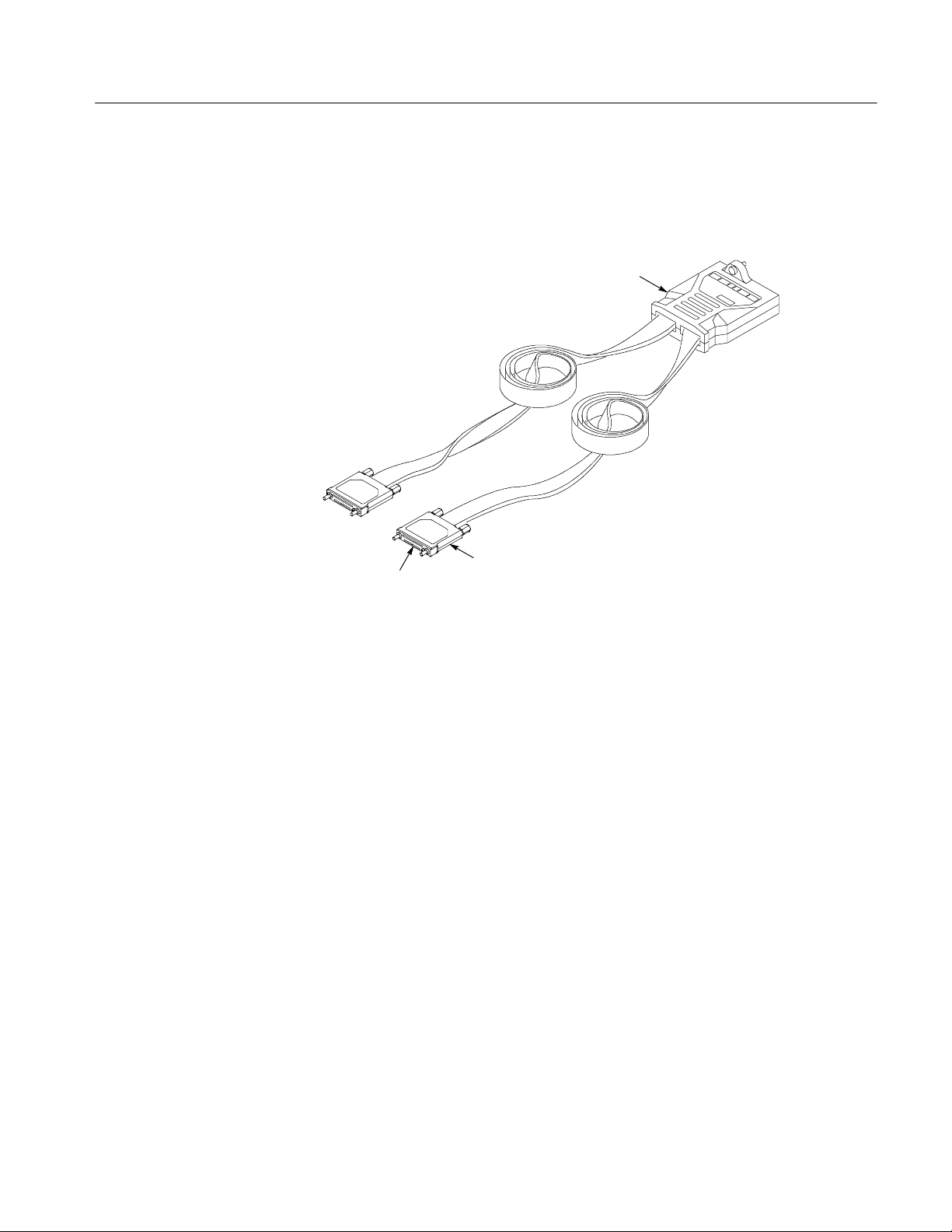
P6860 High-Density Probe
The P6860 Probe is a 34-channel, high-density probe (see Figure 1--3) consisting of two independent probe heads of 17 channel connectors each (16 data and
1 clock/qual).
34 Channel probe to
TLA7Axx module
17--Channel probe head
Elastomer holders (thick
gray or thin black)
Figure 1- 3: P6860 High-Density probe
The following list details the capabilities and qualities of the P6860 Probe:
H Differential or single-ended clock and qualification inputs
H Single-ended data inputs
H Compression contact eliminates need for built-in connector
H Land pattern supports direct signal pass-through
H Supports PCB thickness of 1.27 mm to 3.81 mm (0.050 in to 0.150 in)
H Consists of two independent probe heads of 17 channels each (16 data and
1 clock/qual)
H Narrow 17-channel probe head makes for easier placement and layout
H 2X mode, (for example, 1:2 demultiplexing) uses single-probe head
H 4X mode, (for example, 1:4 demultiplexing) uses one-half of the probe head
H Similar channel density to current Mictor connectors
H Color-coded keyed signal connectors
P68XX Series Logic Analyzer Probes Instruction Manual
1- 5
Page 26
Operating Basics
H Adapter supports Mictor-based connections
H --2.5 V to +5 V input operating range
H --2.0 V to +4.5 V threshold range
H 300 mV minimum single-ended signal amplitude
H 150 mV amplitude each side minimum differential signal
H Minimal loading of 0.7 pF @ 20 kΩ to ground loading
H Operation in normal or inverted polarity is acceptable (clock only)
H Any common mode voltage is acceptable so long as the maximum positive
voltage does not exceed +5 V and the maximum negative voltage does not
exceed --2.5 V (clock only)
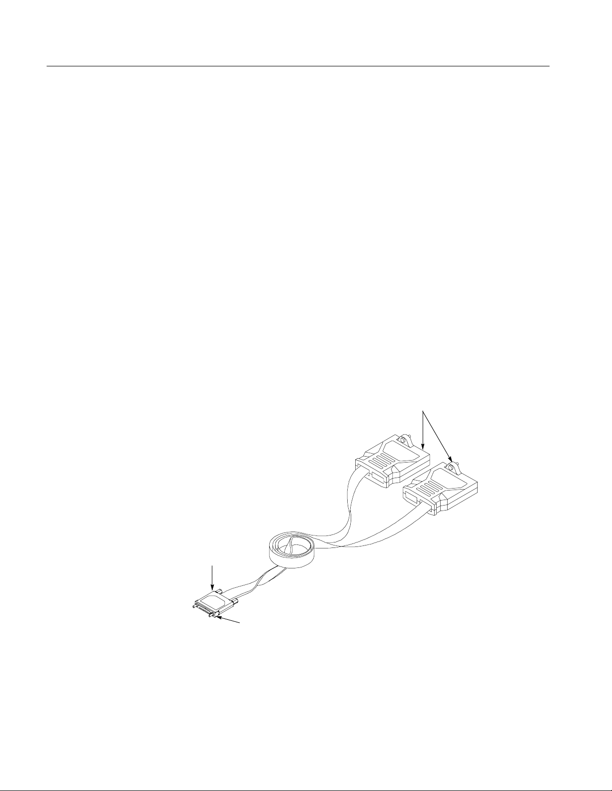
P6864 High- Density 4X
Probe
The P6864 Probe is a 17-channel, high-density 4X probe (see Figure 1--4)
consisting of a single independent probe head containing 17 channel connectors
(16 data and 1 clock/qual) and two module connectors.
8 Channel probe to TLA74xx module
(one of the module end connectors
includes a clock channel)
17 Channel
probe head
1- 6
Elastomer holder (thick gray or thin black)
Figure 1- 4: P6864 High-Density 4X probe
P68XX Series Logic Analyzer Probes Instruction Manual
Page 27

Operating Basics
The following list details the capabilities and qualities of the P6864 probe:
H Differential or single-ended clock and qualification inputs
H Single-ended data inputs
H Compression contact eliminates need for built-in connector
H Land pattern supports direct signal pass-through
H Supports PCB thickness of 1.27 mm to 3.81 mm (0.050 in to 0.150 in)
H Consists of one independent probe head containing 17 channels (16 data and
1 clock/qual)
H Narrow 17-channel probe head makes for increased placement and layout
density when using 4X mode, (for example, 1:4 demultiplexing)
H Color-coded keyed signal connectors
H --2.5 V to +5 V input operating range
H --2.0 V to +4.5 V threshold range
H 300 mV minimum single-ended signal amplitude
H 150 mV minimum each side of a differential signal amplitude
H Minimal loading of 0.7 pF @ 20 kΩ to ground loading
H Operation in normal or inverted polarity is acceptable (clock only)
H Any common mode voltage is acceptable so long as the maximum positive
voltage does not exceed +5 V and the maximum negative voltage does not
exceed --2.5 V (clock only)
P68XX Series Logic Analyzer Probes Instruction Manual
1- 7
Page 28
Operating Basics
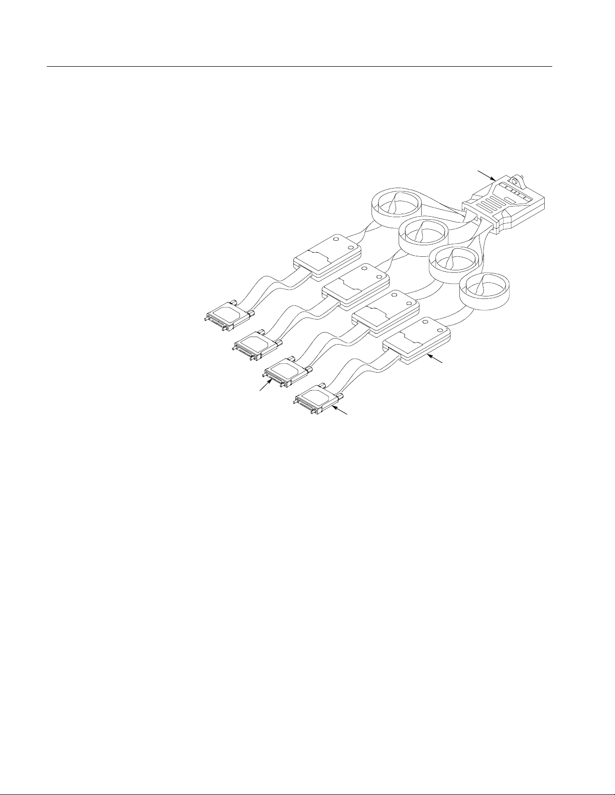
P6880 High-Density
Differential Probe
The P6880 Probe is a 34-channel, high-density differential probe
(see Figure 1--5) consisting of four independent probe heads of 8/9 channels
each.
34 Channel probe to
TLA7Axx module
Way stations
Elastomer holders
(thick gray or thin
black)
8--/9--Channel probe
heads
Figure 1- 5: P6880 High-Density Differential probe
The following list details the capabilities and qualities of the P6880 Probe:
H High-density probe mechanical packaging at half the channel density in the
probe head
H Differential data, clock and qualification inputs (single-ended signals may be
probed if negative input is grounded)
H Same compression land pattern as High-Density Probe eliminates need for
built-in connector
H Land pattern supports direct signal pass-through
H Supports PCB thickness of 1.27 mm to 3.81 mm (0.050 in to 0.150 in)
H Consists of four probe heads supporting 8/9 channels each (nine with
clock/qual) for a total of 34 channels
H 2X mode (1:2 demultiplexing) and 4X mode (1:4 demultiplexing), use two
and one probe head(s) respectively to minimize required board real estate
1- 8
P68XX Series Logic Analyzer Probes Instruction Manual
Page 29

Operating Basics
H Color-coded keyed signal connectors
H --2.5 V to +5 V input operating range
H --2.0 V to +4.5 V threshold range
H 300 mV minimum single-ended signal amplitude (5 V maximum)
H 150 mV each side minimum differential signal amplitude (2.5 V maximum)
H Minimal loading of 0.7 pF @ 20 kΩ to ground loading
H Operation in normal or inverted polarity is acceptable
H Any common mode voltage is acceptable so long as the maximum positive
voltage does not exceed +5 V and the maximum negative voltage does not
exceed --2.5 V
NOTE. Refer to Figure 2--6 on page 2-27 for P6880 probe routing and pin out
information.
Mictor-on-PCB to P6860
Compression Adapter
The Mictor-on-PCB to P6860 Compression adapter (see Figure 1--6) allows
existing microprocessor support packages and your hardware designs with
embedded Mictor connectors to be connected to the P6860 High-Density Probe.
The CLK pin on the Mictor is connected to the CLK+ pin of the compression
footprint. The CLK-- pin of the compression footprint is tied to ground. This
allows the differential clock input of the P6860 probe to function as a
single-ended signal.
This adapter supports standard Mictor connector footprints and signal connections on older logic analyzer designs.
Differential qualification and clock signals are not supported through the
Mictor-on-PCB to Compression adapter due to Mictor footprint limitations (only
+ side of clock and qual signals are supported).
The Mictor adapter adds 2.7 pF to the high-density compression probe load of
0.7 pF for a combined adapter and probe capacitance load of 3.4 pF.
P68XX Series Logic Analyzer Probes Instruction Manual
1- 9
Page 30
Operating Basics
Probe head
label
32.20 mm
(1.268 in)
J2
J1
Compression
adapter
Mictor adapter
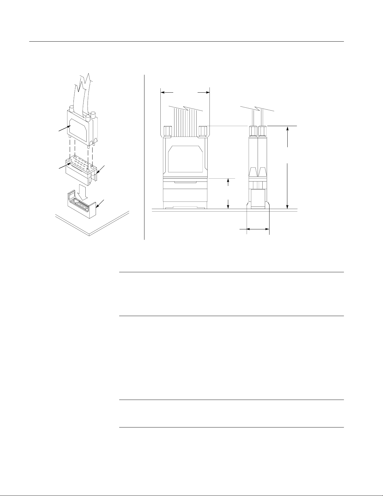
Figure 1- 6: Mictor-on-PCB to P6860 Compression adapter
NOTE. The compression adapter is labeled with J1 and J2 signal identifiers to
assist you with correctly locating the probe heads on the compression adapter
(see Figure 1--6). Each probe-head label contains channel information that you
compare with information contained in the Signal-name column of the Table
2--13 on page 2--16 to determine the signal to which you connect the probe head.
See Figure 1--8 on page 1--12 for comparing the clearances between the P6434
and P68xx probes.
58.57 mm
(2.306 in)
20.17 mm
(.794 in)
12.83 mm
(.505 in)
Compression-on-PCB to
P6434 Mictor Adapter
1- 10
The Compression-on-PCB to P6434 Mictor adapter (see Figure 1--7) allows the
TLA5000, TLA6xx, and TLA7Lx/Mx/Nx/Px/Qx logic analyzers using a P6434
Probe to take advantage of the new compression footprint and eliminate the need
for Mictor connectors in your target system.
NOTE. To use the P6434 adapter, do not install press-in nuts. However, if board
thickness is > .093 in, you will need to install press-in nuts before migrating to
P68xx probes.
P68XX Series Logic Analyzer Probes Instruction Manual
Page 31

Mictor
adapter
Operating Basics
Two different screw lengths are required to accommodate the
1.27 mm to 3.81 mm (0.050 in to 0.150 in) PCB thickness range.
This adapter requires the use of the Compression-on-PCB to P6434 Mictor
adapter land footprint. See Figure 2--8 on page 2--30 for further dimensional
information.
The Compression-on--PCB to Mictor adapter adds 1.5 pF to the P6434 probe
load of 2.0 pF for a combined adapter and probe capacitance load of 3.5 pF.
Elastomer
holder
Circuit board
Adapter
backing plate
32.131 mm
(1.265 in)
15.82 mm
(.623 in)
Figure 1- 7: 34-Channel Compression-on-PCB to P6434 Mictor adapter
To compare the clearance between the P6434 Probe connection and the P6434
Probe connection using the 34-Channel Compression-on-PCB to P6434 Mictor
adapter refer to Figure 1--8. Note that the difference in clearance between the
P6434 Probe connection and the P6434 Probe connection using the C ompression-on-PCB to P6434 Mictor adapter is 3.68 mm (0.145 in).
13.716 mm
(.540 in)
3.81 mm 1.27 mm (.150 in)
(.050 in) PCB Thickness
4.572 mm
(.180 in)
NOTE. In addition to the 34-Channel Compression-on-PCB to P6434 Mictor
adapter, Tektronix also offers a 17-Channel Compression to Mictor adapter. This
17-channel adapter is essentially identical to the 34-channel adapter except that
the posts that go through the circuit board are mounted such that it can connect
to a single 17-channel footprint instead of two 17-channel footprints in a
side-by-side configuration (see Figure 5--5 on page 5--7 in the Replaceable Parts
section of this manual for an illustration of both adapters.
P68XX Series Logic Analyzer Probes Instruction Manual
1- 11
Page 32

Operating Basics
P6434
Mictor adapter
32.131 mm
(1.265 in)
15.82 mm
(.623 in)
3.68 mm
(.145 in)
13.716 mm
(.540 in)
34.93 mm
(1.375 in)
Figure 1- 8: Clearance for probe connection using Compression-on-PCB to P6434 Mictor adapter
Attaching Probe Labels
1- 12
When you purchase a TLA7Axx logic analyzer module, you receive the probes
with all labels already attached.
However, if you purchase additional probes for the logic analyzer module, you
will need to apply the color-coded labels. You will find a detailed description of
how to attach the labels in the following instructions:
H P6810 General Purpose Logic Analyzer Probe Label Instructions
H P6860 High Density Logic Analyzer Probe Label Instructions
H P6864 High Density 4X Logic Analyzer Probe Label Instructions
H P6880 High Density Differential Logic Analyzer Probe Label Instructions
P68XX Series Logic Analyzer Probes Instruction Manual
Page 33

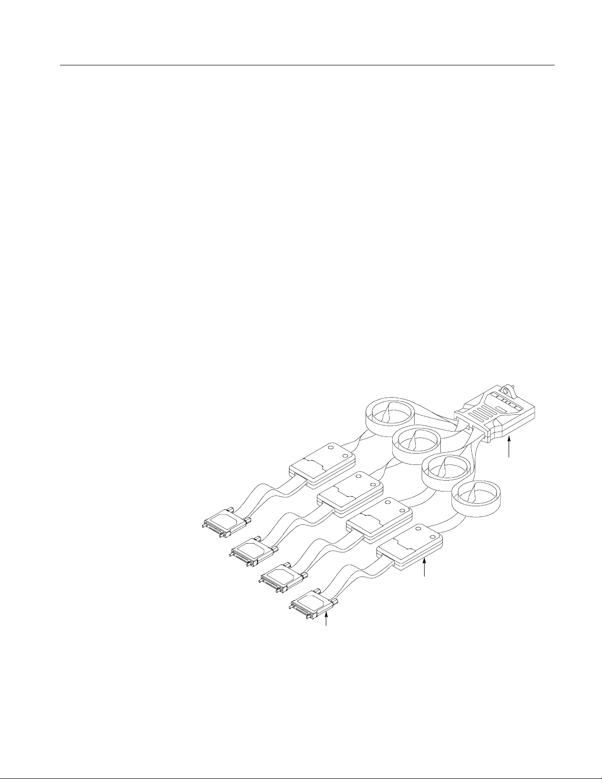
Connecting the Probes to the Logic Analyzer
Refer to Figure 1--9 and connect the probes to the logic analyzer according to the
following steps.
1. Identify the beveled edges of the connector inside the module end of the
probe.
2. Align the beveled edges of the connector to its mating connector on the logic
analyzer module and press into place.
3. Use care to evenly tighten both screws on the module end of the probe until
they are snug. First slightly tighten both screws, then snug each screw to
4 in-lbs (max).
NOTE. All P68xx series Logic Analyzer probes can be connected to the logic
analyzer when it is powered up. In addition, all P68xx series Logic Analyzer
probes connect to the logic analyzer in exactly the same manner.
Operating Basics
Probe
Figure 1- 9: Connecting the probes to the logic analyzer
Match
color--coded
labels
P68XX Series Logic Analyzer Probes Instruction Manual
1- 13
Page 34

Operating Basics
Cleaning the P686x and P6880 Compression Footprints
CAUTION. To avoid electrical damage, always turn off the power of your target
system before cleaning the compression footprint.
Prior to connecting the probe to the target system, the compression footprints on
the your board must be properly cleaned. Clean the compression footprints
according to the following steps:
1. Use a lint-free cloth moistened with isopropyl alcohol and gently wipe the
footprint surface.
2. Remove any remaining lint using a nitrogen air gun.
NOTE. Use alcohol sparingly and be sure that you have removed any remaining
lint or residue with the nitrogen air gun.
Cleaning the P686x and P6880 Probe Heads
Before connecting the P686x and P6880 Probes to the target system, ensure that
the probe heads are free from dust, dirt, and contaminants. If necessary, clean the
probe heads according to the following steps.
CAUTION. Static discharge can damage semiconductor components in the probe
head. Always wear a grounded antistatic wrist strap whenever handling the
probe head. Also verify that anything to which the probe head is connected does
not carry a static charge.
NOTE. Never clean the elastomers. Always replace them instead. Refer to the
Replaceable Parts section of this manual for information on ordering parts.
1. Remove elastomer holder.
2. Moisten a cotton swab with isopropyl alcohol.
1- 14
P68XX Series Logic Analyzer Probes Instruction Manual
Page 35

Operating Basics
Elastomer holder
Figure 1- 10: Cleaning the probe heads
3. Gently wipe the edge print pads of the hybrid.
4. Remove any remaining lint using a nitrogen air gun.
5. Put the elastomer holder back in place.
CAUTION. Be careful not to touch the elastomers to avoid damaging the probe
contacts. Also, do not reverse the elastomer as this will transfer contaminants.
Print pads
Storing the P686x and P6880 Probe Heads
To protect the elastomer, it is important to properly store the probe heads when
the probes are not in use. See Figure 1--11.
1. Locate the keying pin on the probe end and align it to the keying pin hole on
the nut bar.
2. While holding the probe end at a perpendicular angle to the nut bar, loosely
attach both probe head screws.
P68XX Series Logic Analyzer Probes Instruction Manual
1- 15
Page 36

Operating Basics
Safely store the
probe head
Nut Bar
Nut Bar
Figure 1- 11: Storing the probe heads
Connecting the Probes to the Target System
Connecting the P6810
General Purpose Probe
Refer to Figure 1--12 and connect the probe to the target system by performing
the steps that follow. You can connect the probe heads to the target system
without turning off the power to the target system.
CAUTION. To avoid damaging the probe and target system, always position the
probe at a perpendicular angle to the mating connector and then connect the
probe. Incorrect handling of the probe while connecting it to the target system
can result in damage to the probe or to the mating connector in the target
system.
1. Connect the probe end to the square pins on the PCB.
2. If using the single-ended leadset, connect the negative input to ground on the
PCB.
or
If using the differential leadset, connect the positive side of the podlet to the
positive side of the signal on the PCB, and the negative side of the podlet to
the negative side of the signal.
1- 16
3. Connect the way station ground to ground on the PCB.
P68XX Series Logic Analyzer Probes Instruction Manual
Page 37

Operating Basics
1
2
3
3
4
5
1 Connect 8 podlets in the podlet holder
directly to square pins on the PCB with
0.100 in pin spacing.
2 Connect 1 podlet directly to the square
pins on the PCB with 2 mm (0.079 in) or
2.54 mm (0.100 in) pin spacing.
3 Connect 1 podlet with 1 channel leadset to the square pin on the PCB with 2 mm (0.079 in) or 2.54 mm
(0.100 in) pin spacing. The negative lead (half--white/half--black housing that contains a damping resistor)
is connected to ground in a single--ended application lead or the minus in a differential application.
4 Connect 8 podlets in the podlet holder with an 8 channel differential leadset to the square pins on the
PCB with 2 mm (0.079 in) or 2.54 mm (0.100 in) pin spacing. The negative lead (half--white/half--black
housing that contains a damping resistor) is connected to the minus in a differential application.
5 Connect 8 podlets in the podlet holder with an 8 channel single--ended leadset to the square pins on the
PCB with 2 mm (0.079 in) or 2.54 mm (0.100 in) pin spacing. The negative lead (total black housing that
contains no damping resistor; however, the leadset housing contains a damping resistor in ground path
for each channel) is connected to ground in a single--ended application lead.
Figure 1- 12: Connecting the P6810 probe to the target system
P68XX Series Logic Analyzer Probes Instruction Manual
1- 17
Page 38

Operating Basics
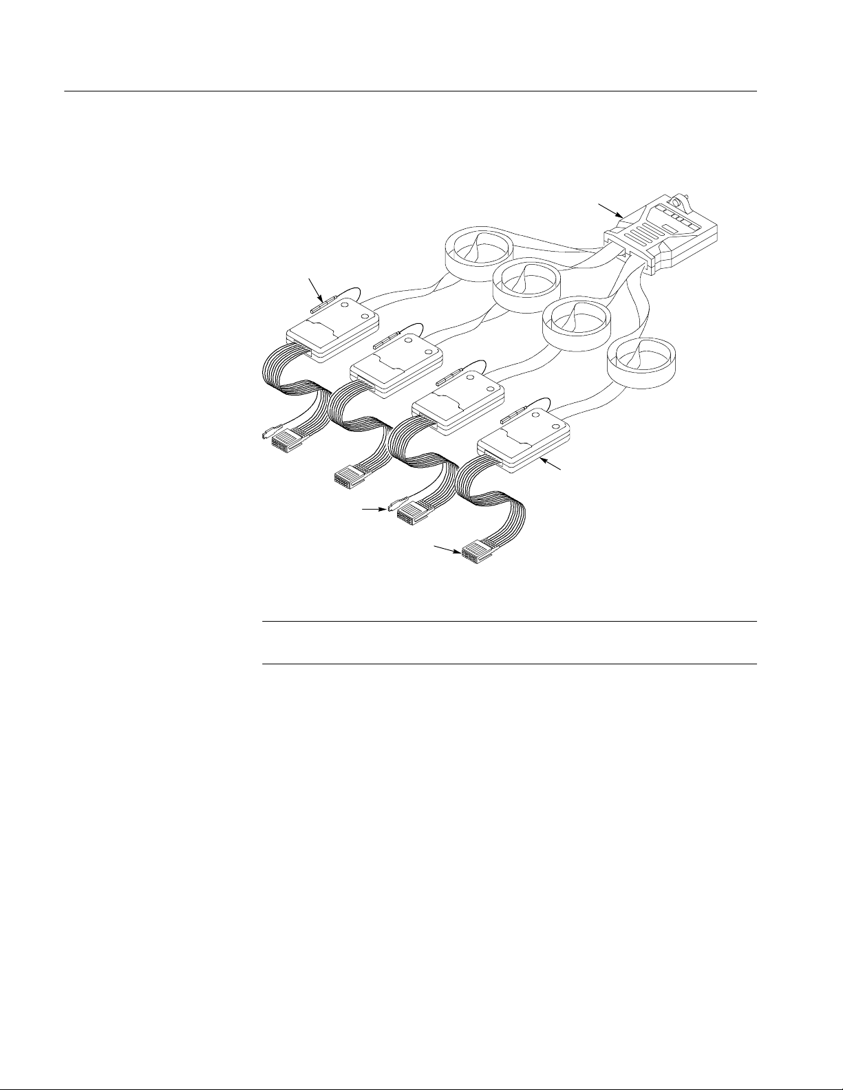
Connecting the P686x
High Density and P6880
Differential Probes
Connect the P686x High-Density and P6880 Differential Probes
(see Figure 1--14) to the target system. You can connect the probes to the target
system without turning off the power to the target system.
Installing the Correct Elastomer Holder. If the PCB is ≤ .093 in, use the thin
elastomer holder with the nut bar. If the PCB is > .093 in, use the thick elastomer
holder with the press-in nuts.
H Nut Bar
1. Press the nut bar backing plate into the two holes on the underside of the
compression footprint on the PCB.
2. Locate the keying pin on the probe end and align it to the keying pin hole on
the PCB.
3. While holding the probe end at a perpendicular angle to the PCB, finger-
tighten (typically,1@2in-lbs) both probe head screws until snug, not to
exceed 1 in-lbs. You are encouraged to use a torque wrench to ensure proper
tightness to the probe-head screws.
CAUTION. When attaching the probe head to the target system, you must use care
to evenly tighten probe head screws until they are snug. First tighten both screws
until the nut bar makes contact with the board surface, then snug each screw to
1 in-lbs (max). Under tightening the probe head screws can result in intermittence. Over tightening can result in damage to the elastomer holder and stripped
screws.
1- 18
H Press-in Nuts
1. Install the press-in nuts on the PCB by following the Manufacturer’s
installation procedure. Refer to Figure 1--13 for press-in nut installation
details.
Keying pin hole
Press--in nuts thread
type (2--56 UNC-2B)
Circuit board
Min 2.362 mm
to Max 3.81 mm
(0.093 in to
0.150 in)
Figure 1- 13: Press-in Nuts installation
P68XX Series Logic Analyzer Probes Instruction Manual
Page 39

Operating Basics
2. Locate the keying pin on the probe end and align it to the keying pin hole on
the PCB.
3. While holding the probe end at a perpendicular angle to the PCB, finger
tighten (typically,
1
@2in-lbs) both probe head screws until snug, not to
exceed 1 in-lbs. You are encouraged to use a torque wrench to ensure proper
tightness to the probe-head screws.
CAUTION. When attaching the probe head to the target system, you must use care
to evenly tighten probe head screws until they are snug. First slightly tighten
both screws, then snug each screw to 1 in-lbs (max). Under tightening the probe
head screws can result in intermittence. Over tightening can result in damage to
the elastomer holder and stripped screws.
P68XX Series Logic Analyzer Probes Instruction Manual
1- 19
Page 40

Operating Basics
Note that elastomer
holder is keyed
Thin black,
(no rib)
Keying pin
Keying pin hole
Press--in nuts
Thick gray,
(rib)
White thin line
is keying pin
Keying pin
Nut Bar
Probe head
label
Compression
adapter
J2
J1
Mictor--on--PCB
(Not applicable
to P6864 probe)
1- 20
Figure 1- 14: Connecting the P686x and P6880 probes to the target system
NOTE. The compression adapter is labeled with J1 and J2 signal identifiers to
assist you with correctly locating the probe heads on the compression adapter
(see Figure 1--6). Each probe-head label contains channel information that you
compare with information contained in the Signal-name column of the Table
2--13 on page 2--16 to determine the signal to which you connect the probe head.
P68XX Series Logic Analyzer Probes Instruction Manual
Page 41

Operating Basics
Connecting the
Mictor-on-PCB to P6860
Compression Adapter
(Applies to P6860 Probe
Only)
The Mictor-on-PCB to P6860 Compression adapter (see Figure 1--6 on
page 1--10) allows existing applications of older logic analyzer modules and
probes to connect to the compression footprint. You can connect the adapter to
the target system without turning off the target system. Connect the adapter
according to the following steps.
NOTE. Be sure to use the thin elastomer holder. A thin elastomer is black and
does not have the protruding rib (see Figure 1--14).
1. While holding the first probe end at a perpendicular angle to the adapter,
place the probe end into the adapter and finger-tighten the screws until snug,
not to exceed 1 in.-lbs.
2. Connect the second probe end to the adapter in the same manner.
3. Press the connected probe ends and adapter into the existing Mictor
connector on the PCB.
This adapter supports standard Mictor connector footprints and signal connections on older logic analyzer designs.
The differential qualification and clock signals are not supported through the
Mictor-on-PCB to P6860 Compression adapter due to the Mictor footprint
limitations (only + side of clock and qual signals are supported).
Connecting the
Compression-on-PCB to
P6434 Mictor Adapter
The Mictor adapter adds 2.7 pF to the High-Density Compression probe load of
0.7 pF for a combined adapter and probe capacitance load of 3.4 pF.
The Compression-on-PCB to P6434 Mictor adapter (see Figure 1--7 on
page 1--11) allows you to connect the compression footprint to the Mictor
connector pins used by the P6434 Probe. You can connect the adapter to the
target system without turning off the target system. Connect the adapter
according to the following steps.
NOTE. To use this adapter do not install press-in nuts. However if board
thickness is >.093 in, you will need to install press-in nuts before migrating to
P68xx probes.
P68XX Series Logic Analyzer Probes Instruction Manual
1- 21
Page 42

Operating Basics
1. Place the adapter at a perpendicular angle on top of the compression
footprint.
2. Place the backing plate on the underside of the PCB.
3. Connect the backing plate by sliding the two screws into the existing screw
1
holes from the underside of the PCB and finger-tighten (typically,
@2in-lbs)
the screws until snug, not to exceed 1 in-lbs. You are encouraged to use a
torque wrench to ensure proper tightness to the probe head screws.
CAUTION. When attaching the probe head to the target system, you must use care
to evenly tighten probe head screws until they are snug. First slightly tighten
both screws, then snug each screw to 1 in-lbs (max). Under tightening the probe
head screws can result in intermittence. Over tightening can result in damage to
the elastomer holder and stripped screws.
4. Plug the P6434 Probe into the adapter.
Screws of two different lengths are provided to attach the adapter to your PCB.
The length of screw you need depends on the thickness of the PCB (0.050 in to
0.150 in).
This adapter requires use of the Compression-on-PCB to P6434 Mictor adapter
land footprint. For further dimensional information refer to the Compression-onPCB to P6434 Mictor adapter land footprint (see Figure 2--8 on page 2--30).
1- 22
P68XX Series Logic Analyzer Probes Instruction Manual
Page 43

Reference
Page 44

Page 45

Reference
This section provides reference information and specifications for the P6810
General Purpose, P6860 High-Density, P 6864 High-Density 4X, and P6880
High-Density Differential Probes. Topics include the following.
H Designing an interface between the probe and a target system
H Specifications
Designing an Interface Between the P68xx Probes and a Target System
Once you have determined which probe is required, use the following information to design the appropriate connector into your target system board. The
following topics are in this section:
H Signal fixturing considerations
H Signal connections (signal names and land footprints)
H Mechanical considerations
Signal Fixturing
Considerations
H Electrical considerations
This section contains the following information to consider for signal fixturing:
H Clocks and qualifiers
H Merged modules and source synchronous clocking
H Demultiplexing multiplexed busses
H 2X and 4X high resolution timing modes (Internal 2X and 4X)
H Probing analog signals
H Range recognition
Clocks and Qualifiers. Every logic analyzer has some special purpose input
channels. Inputs designated as clocks can cause the analyzer to store data.
Qualifier channels can be logically AND’ed and OR’ed with clocks to further
define when the analyzer should latch data from the system under test. R outing
the appropriate signals from our design to these inputs ensures that the logic
analyzer can acquire data correctly. Unused clocks can be used as qualifier
signals.
P68XX Series Logic Analyzer Probes Instruction Manual
2- 1
Page 46

Reference
TLA7Axx
Depending on the channel width, each TLA7Axx Series logic analyzer module
will have different set of clock and qualifier channels. Table 2--1 shows the clock
and qualifier channels available for each module.
Table 2- 1: Logic analyzer clock and qualifier availability
Clock Inputs Qualifier Inputs
Module
TLA7AA1 n n
TLA7AA2 n n n n
TLA7AA3 n n n n n n
TLA7AA4 n n n n n n n n
TLA7AB2 n n n n
TLA7AB4 n n n n n n n n
CLK:0
CLK:1 CLK:2 CLK:3 QUAL:0 QUAL:1 QUAL:2 QUAL:3
All clock and qualifier channels are stored. The analyzer always stores the logic
state of these channels every time it latches data.
Since clock and qualifier channels are stored in the analyzer memory there is no
need to double probe these signals for timing analysis. When switching from
state to timing analysis modes all of the clock and qualifier signals will be
visible. This also allows you to route regular signals, those not needed for
clocking, to these channels when they are not being used for their special
purpose.
It is a good practice to take advantage of these channels to increase your options
for when you will latch data. Routing several of your design’s clocks and strobes
to the analyzer clock inputs will provide you with a greater flexibility in the
logic analyzer clocking setup menus.
As an example, look at a microprocessor with a master clock, data strobe, and an
address strobe. Routing all three of these signals to analyzer clock inputs will
enable you to latch data on the processor master clock, only when data is
strobed, or only when address is strobed. Some forethought in signal routing can
greatly expand the ways in which you can latch and analyze data.
A microprocessor also provides a good example of signals that can be useful as
qualifiers. There are often signals that indicate data reads versus data writes
(R/W), signals that show when alternate bus masters have control of the
processor busses (DMA), and signals that show when various memory devices
are being used (ChipSel). All of these signals are good candidates for assignment
to qualifier channels.
By logically AND’ing the clock with one of these qualifiers you can program the
analyzer to store only data reads or data writes. Using the DMA signal as a
2- 2
P68XX Series Logic Analyzer Probes Instruction Manual
Page 47

Reference
qualifier provides a means of filtering out alternate bus master cycles. Chip
selects can limit data latching to specific memory banks, I/O ports, or peripheral
devices.
Merged Module Sets and Source Synchronous Clocking. TLA7Axx analyzer
modules that are 102 channels or 136 channels wide can be merged together to
act as a single logic analyzer with a larger channel count. Up to five modules can
be merged to provide up to a 680 channel analyzer. A unique feature of the
TLA7Axx module is that it supports source synchronous clocking. Combining
these two capabilities provide some additional considerations for signal routing.
Source synchronous clocking is a method which manages the skew between the
system clock and the data bus by requiring the sending device to drive an actual
clock or strobe signal along with the data that is very tightly coupled with it in
terms of skew. The receiving device then uses this strobe to capture the data.
A variant of this scheme is being applied to large microprocessor busses, where
the bus is split into smaller, more easily managed groups that each have their
own dedicated strobe. Although the timing relationship between a particular
clock and its associated data group is very tight, the timing between the different
groups can vary greatly and changes depending on which device has control of
the bus.
Many source synchronous designs use wide busses. It is not uncommon to
require a set of merged logic analyzer modules to provide the channel count
needed in probing larger source synchronous systems. While all of the modules
in a merged set can use their clock inputs independently if needed, it must be
remembered that there are a maximum of four clock inputs on a 136 channel
wide module.
To see the importance of this reminder we will once again use a microprocessor
system as an example. Tektronix logic analyzer processor has a 32 bit address
bus and a 64 bit data bus. The data bus is split into four 16 bit subgroups that
have independent source synchronous clocks. For the logic analyzer to correctly
acquire data from this system it will need five clock inputs, one for the address
bus and one each for the four 16 bit data bus subgroups.
To acquire both busses the analyzer would need at least 96 channels (32 address
and 64 data). However, a single 102 channel card doesn’t have the required five
clock inputs. By merging two 102 channel modules into a set you can obtain the
needed number of clock inputs. Route the address bus to one module in the set
and route the data bus, along with its four source synchronous clocks, to the
second module in the set.
Demultiplexing Multiplexed Busses. TLA7Axx module supports both 2X and 4X
demultiplexing. Each signal on a dual or quad multiplexed bus can be demultiplexed into its own logic analyzer channel. See Tables 2--2 and 2--3 to determine
P68XX Series Logic Analyzer Probes Instruction Manual
2- 3
Page 48

Reference
which channel groups to connect to feed channels in the target system the test
data.
Table 2- 2: 2X Demultiplexing source-to-destination channel assignments
Source
connecting
channel groups
A3:7--0 D3:7--0 D3:7--0 C3:7--0 C3:7--0 D3:7--0 C3:7--0
A2:7--0 D2:7--0 D2:7--0 C2:7--0 C2:7--0 D2:7--0 C2:7--0
A1:7--0 D1:7--0 D1:7--0 D1:7--0 D1:7--0 D1:7--0
A0:7--0 D0:7--0 D0:7--0 D0:7--0 D0:7--0 D0:7--0
C3:7--0 C1:7--0 C1:7--0 C1:7--0
C2:7--0 C0:7--0 C0:7--0 C0:7--0
E3:7--0 E1:7--0 E1:7--0
E2:7--0 E0:7--0 E0:7--0
CLK:0 QUAL:1 QUAL:1 QUAL:1
CLK:1 QUAL:0 QUAL:0 QUAL:0
CLK:2 QUAL:3 QUAL:3
CLK:3 QUAL:2 QUAL:2
Destination channels receiving target system test data
TLA7AA4 TLA7AA3 TLA7AA2 TLA7AA1 TLA7AB4 TLA7AB2
2- 4
P68XX Series Logic Analyzer Probes Instruction Manual
Page 49

Table 2- 3: 4X Demultiplexing source-to-destination channel assignments
Reference
Source
connecting
channel groups
C3:7--0 C2:7--0
A1:7--0 A0:7--0
A3:7--0 A2:7--0
E3:7--0 E2:7--0
CLK:3 CLK:2
CLK:1 CLK:0
Destination channels receiving target system test data
TLA7AA4 TLA7AA3 TLA7AA2 TLA7AA1 TLA7AB4 TLA7AB2
C1:7--0
C0:7--0
D1:7--0
D0:7--0
D3:7--0
D2:7--0
E1:7--0
E0:7--0
QUAL:3
QUAL:2
QUAL:1
QUAL:0
C2:7--0
C1:7--0
C0:7--0
A0:7--0
D1:7--0
D0:7--0
A2:7--0
D3:7--0
D2:7--0
CLK:0
QUAL:1
QUAL:0
A3:7--0
A2:7--0
C2:7--0
A0:7--0
D1:7--0
D0:7--0
A3:7--0
A2:7--0
C2:7--0
C2:7--0
C1:7--0
C0:7--0
A0:7--0
D1:7--0
D0:7--0
A2:7--0
D3:7--0
D2:7--0
E2:7--0
E1:7--0
E0:7--0
CLK:2
QUAL:3
QUAL:2
CLK:0
QUAL:1
QUAL:0
A3:7--0
A2:7--0
C2:7--0
A0:7--0
D1:7--0
D0:7--0
When demultiplexing data there is no need to connect the destination channels to
the multiplexed bus. Data from the source channels are routed to the destination
channels internal to the logic analyzer. Tables 2--2 and 2--3 show the mapping of
source channels to destination channels.
Demultiplexing affects only the main memory for the destination channels. This
means that the MagniVu memory is filled with data from whatever is connected
to the demultiplexing destination channel probe inputs. This provides an
opportunity to acquire high resolution MagniVu data on a few extra channels.
Connecting the demultiplexing destination channels to other signals will allow
viewing of their activity in the MagniVu memory but not the main memory.
2X and 4X High Resolution Timing Modes. 2X high resolution timing mode
provides double the normal 500 MHz sample rate on one half of the channels.
By trading half of the analyzers channels the remaining channels can be sampled
at a 1 GHz rate with double the memory depth. 4X high resolution timing mode
provides quadruple the normal 500 MHz sample rate on one fourth of the
channels. By trading three-fourths of the analyzers channels the remaining
channels can be sampled at a 2 GHz rate with quadruple the memory depth.
P68XX Series Logic Analyzer Probes Instruction Manual
2- 5
Page 50

Reference
Both of the high resolution timing modes use the same demultiplexing channel
routingasshowninTables2--2and2--3.Bytakingcaretoassigncriticalsignals
to the demultiplexing source channels you can obtain extra timing resolution
where most needed. Since demultiplexing affects only the main memory you will
still have the MagniVu data available for all of the signals that are disconnected
from the main memory when you switch to the high resolution timing modes.
Probing Analog Signals. TLA7Axx module provides visibility of analog signals
with iView. iView routes the actual signal seen by each channel’s probe through
a high bandwidth path to an analog multiplexer inside of the logic analyzer
module. From the logic analyzer interface you can route any input channel to one
of four output connectors on the module. By connecting the analyzer iView
analog probe outputs to your oscilloscope you can see the analog characteristics
of any signal probed by the logic analyzer.
Sometimes there are analog signals that would be convenient to have fixtured for
easier probing. Signals such as A/D Converter inputs, D/A C onverter outputs,
low voltage power supplies, termination voltages, and oscillator outputs are just
a few examples. Routing these signals to unused logic analyzer inputs provides a
quick method of viewing their activity without ever picking up a scope probe.
Signal Names
Care must be taken to ensure that such signals are voltage limited and will not
exceed the maximum nondestructive input voltage for the logic analyzer probes
of ±15 Vpeak.
Range Recognition. When using range recognizers, the probe groups and probe
channels must be in hardware order. Probe groups must be used from the
most-significant probe group to the least-significant probe group based on the
following order:
C3 C2 C1 C0 E3 E2 E1 E0 A3 A2 D3 D2 A1 A0 D1 D0 Q3 Q2 Q1 Q0 CK3
CK2 CK1 CK0
Probe channels must be from the most-significant channel to the least-significant
channel based on the following order:
76543210
The above examples assumes a 136-channel LA module. The missing channels
in LA modules with fewer than 136 channels are ignored. With merged modules,
range recognition extends across the first three modules: the master module
contains the most-significant channels.
See Tables 2--4 through 2--14 for the P6810, P6860, P6864, and P6880 Probes
and adapters signal connections. Match the alpha character that precedes the
channel identifier (for example, E3:7) to the probe head label. This will simplify
probe connections to the logic analyzer when you use the following tables.
2- 6
P68XX Series Logic Analyzer Probes Instruction Manual
Page 51

Table 2- 4: P6810 Probe signal connections on 136 and 102 channel modules for probe #4 and probe #3
136 channel module
102 channel module
Land Pattern Probe #4 Probe #3
Reference
Signal
name
Clk/Qual Clk/Qual Q3-- Q2-- CK0-- Q0--
Clk/Qual+ Clk/Qual Q3+ Q2+ CK0+ Q0+
Data 7-- 7 E3:7-- E2:7-- E1:7-- E0:7-- A3:7-- A2:7-- D3:7-- D2:7--
Data 7+ 7 E3:7+ E2:7+ E1:7+ E0:7+ A3:7+ A2:7+ D3:7+ D2:7+
Data 6-- 6 E3:6-- E2:6-- E1:6-- E0:6-- A3:6-- A2:6-- D3:6-- D2:6--
Data 6+ 6 E3:6+ E2:6+ E1:6+ E0:6+ A3:6+ A2:6+ D3:6+ D2:6+
Data 5-- 5 E3:5-- E2:5-- E1:5-- E0:5-- A3:5-- A2:5-- D3:5-- D2:5--
Data 5+ 5 E3:5+ E2:5+ E1:5+ E0:5+ A3:5+ A2:5+ D3:5+ D2:5+
Data 4-- 4 E3:4-- E2:4-- E1:4-- E0:4-- A3:4-- A2:4-- D3:4-- D2:4--
Data 4+ 4 E3:4+ E2:4+ E1:4+ E0:4+ A3:4+ A2:4+ D3:4+ D2:4+
Data 3-- 3 E3:3-- E2:3-- E1:3-- E0:3-- A3:3-- A2:3-- D3:3-- D2:3--
Data 3+ 3 E3:3+ E2:3+ E1:3+ E0:3+ A3:3+ A2:3+ D3:3+ D2:3+
Data 2-- 2 E3:2-- E2:2-- E1:2-- E0:2-- A3:2-- A2:2-- D3:2-- D2:2--
Data 2+ 2 E3:2+ E2:2+ E1:2+ E0:2+ A3:2+ A2:2+ D3:2+ D2:2+
Data 1-- 1 E3:1-- E2:1-- E1:1-- E0:1-- A3:1-- A2:1-- D3:1-- D2:1--
Data 1+ 1 E3:1+ E2:1+ E1:1+ E0:1+ A3:1+ A2:1+ D3:1+ D2:1+
Data 0-- 0 E3:0-- E2:0-- E1:0-- E0:0-- A3:0-- A2:0-- D3:0-- D2:0--
Data 0+ 0 E3:0+ E2:0+ E1:0+ E0:0+ A3:0+ A2:0+ D3:0+ D2:0+
Refer to Table 2- 2 on page 2- 4 and Table 2- 3 on page 2- 5 for 2X and 4X demultiplexing channel assignments.
Podlet Way
Station
Way
Station
Way
Station
Way
Station
Way
Station
Way
Station
Way
Station
Way
Station
Any differential input, either the differential clock/qualifiers on the P686x High-density Probe, or all differential data and
clock/qualifiers on the P6810 General Purpose Differential Probe and P6880 High-density Differential Probe, may have
their negative input pin grounded and be used as a single-ended input.
P68XX Series Logic Analyzer Probes Instruction Manual
2- 7
Page 52

Reference
Table 2- 5: P6810 Probe signal connections on 102 and 136 channel modules for probe #2 and probe #1
Land Pattern Probe #2 Probe #1
Signal
name
Clk/Qual-- Clk/Qual-- CK1-- CK2-- CK3-- Q1--
Clk/Qual+ Clk/Qual+ CK1+ CK2+ CK3+ Q1+
Data 7-- 7 A1:7-- A0:7-- D1:7-- D0:7-- C3:7-- C2:7-- C1:7-- C0:7--
Data 7+ 7 A1:7+ A0:7+ D1:7+ D0:7+ C3:7+ C2:7+ C1:7+ C0:7+
Data 6-- 6 A1:6-- A0:6-- D1:6-- D0:6-- C3:6-- C2:6-- C1:6-- C0:6--
Data 6+ 6 A1:6+ A0:6+ D1:6+ D0:6+ C3:6+ C2:6+ C1:6+ C0:6+
Data 5-- 5 A1:5-- A0:5-- D1:5-- D0:5-- C3:5-- C2:5-- C1:5-- C0:5--
Data 5+ 5 A1:5+ A0:5+ D1:5+ D0:5+ C3:5+ C2:5+ C1:5+ C0:5+
Data 4-- 4 A1:4-- A0:4-- D1:4-- D0:4-- C3:4-- C2:4-- C1:4-- C0:4--
Data 4+ 4 A1:4+ A0:4+ D1:4+ D0:4+ C3:4+ C2:4+ C1:4+ C0:4+
Data 2+ 2 A1:2+ A0:2+ D1:2+ D0:2+ C3:2+ C2:2+ C1:2+ C0:2+
Data 3-- 3 A1:3-- A0:3-- D1:3-- D0:3-- C3:3-- C2:3-- C1:3-- C0:3--
Data 3+ 3 A1:3+ A0:3+ D1:3+ D0:3+ C3:3+ C2:3+ C1:3+ C0:3+
Data 2-- 2 A1:2-- A0:2-- D1:2-- D0:2-- C3:2-- C2:2-- C1:2-- C0:2--
Data 1-- 1 A1:1-- A0:1-- D1:1-- D0:1-- C3:1-- C2:1-- C1:1-- C0:1--
Data 1+ 1 A1:1+ A0:1+ D1:1+ D0:1+ C3:1+ C2:1+ C1:1+ C0:1+
Data 0-- 0 A1:0-- A0:0-- D1:0-- D0:0-- C3:0-- C2:0-- C1:0-- C0:0--
Data 0+ 0 A1:0+ A0:0+ D1:0+ D0:0+ C3:0+ C2:0+ C1:0+ C0:0+
Refer to Table 2- 2 on page 2- 4 and Table 2- 3 on page 2- 5 for 2X and 4X demultiplexing channel assignments.
Podlet Way
Station
Way
Station
Way
Station
Way
Station
Way
Station
Way
Station
Way
Station
Way
Station
Any differential input, either the differential clock/qualifiers on the P686x High-density Probe, or all differential data and
clock/qualifiers on the P6810 General Purpose Differential Probe and P6880 High-density Differential Probe, may have
their negative input pin grounded and be used as a single-ended input.
2- 8
P68XX Series Logic Analyzer Probes Instruction Manual
Page 53

Table 2- 6: P6810 Probe signal connections on 68 and 34 channel modules
68 channel module
34 channel module
Land Pattern Probe #2 Probe #1
Reference
Signal
name
Clk/Qual Clk/Qual CK1-- CK2-- CK3-- CK0--
Clk/Qual+ Clk/Qual CK1+ CK2+ CK3+ CK0+
Data 7-- 7 A1:7-- A0:7-- D1:7-- D0:7-- C3:7-- C2:7-- A3:7-- A2:7--
Data 7+ 7 A1:7+ A0:7+ D1:7+ D0:7+ C3:7+ C2:7+ A3:7+ A2:7+
Data 6-- 6 A1:6-- A0:6-- D1:6-- D0:6-- C3:6-- C2:6-- A3:6-- A2:6--
Data 6+ 6 A1:6+ A0:6+ D1:6+ D0:6+ C3:6+ C2:6+ A3:6+ A2:6+
Data 5-- 5 A1:5-- A0:5-- D1:5-- D0:5-- C3:5-- C2:5-- A3:5-- A2:5--
Data 5+ 5 A1:5+ A0:5+ D1:5+ D0:5+ C3:5+ C2:5+ A3:5+ A2:5+
Data 4-- 4 A1:4-- A0:4-- D1:4-- D0:4-- C3:4-- C2:4-- A3:4-- A2:4--
Data 4+ 4 A1:4+ A0:4+ D1:4+ D0:4+ C3:4+ C2:4+ A3:4+ A2:4+
Data 3-- 3 A1:3-- A0:3-- D1:3-- D0:3-- C3:3-- C2:3-- A3:3-- A2:3--
Data 3+ 3 A1:3+ A0:3+ D1:3+ D0:3+ C3:3+ C2:3+ A3:3+ A2:3+
Data 2-- 2 A1:2-- A0:2-- D1:2-- D0:2-- C3:2-- C2:2-- A3:2-- A2:2--
Data 2+ 2 A1:2+ A0:2+ D1:2+ D0:2+ C3:2+ C2:2+ A3:2+ A2:2+
Data 1-- 1 A1:1-- A0:1-- D1:1-- D0:1-- C3:1-- C2:1-- A3:1-- A2:1--
Data 1+ 1 A1:1+ A0:1+ D1:1+ D0:1+ C3:1+ C2:1+ A3:1+ A2:1+
Data 0-- 0 A1:0-- A0:0-- D1:0-- D0:0-- C3:0-- C2:0-- A3:0-- A2:0--
Data 0+ 0 A1:0+ A0:0+ D1:0+ D0:0+ C3:0+ C2:0+ A3:0+ A2:0+
Refer to Table 2- 2 on page 2- 4 and Table 2- 3 on page 2- 5 for 2X and 4X demultiplexing channel assignments.
Podlet Way
Station
Way
Station
Way
Station
Way
Station
Way
Station
Way
Station
Way
Station
Way
Station
Any differential input, either the differential clock/qualifiers on the P686x High-density Probe, or all differential data and
clock/qualifiers on the P6810 General Purpose Differential Probe and P6880 High-density Differential Probe, may have
their negative input pin grounded and be used as a single-ended input.
P68XX Series Logic Analyzer Probes Instruction Manual
2- 9
Page 54

Reference
Table 2- 7: P6860 High-Density Probe channel mapping on 136 and 102 channel modules
136 channel module
102 channel module
Land Pattern Probe #4 Probe #3 Probe #2 Probe #1
Signal
name
Clk/Qual-- A15 Q3-- Q2-- CK0-- Q0-- CK1-- CK2-- CK3-- Q1--
GND A14 GND GND GND GND GND GND GND GND
Clk/Qual+ A13 Q3+ Q2+ CK0+ Q0+ CK1+ CK2+ CK3+ Q1+
Data 15 B12 E3:7 E1:7 A3:7 D3:7 A1:7 D1:7 C3:7 C1:7
GND B11 GND GND GND GND GND GND GND GND
Data 14 B10 E3:6 E1:6 A3:6 D3:6 A1:6 D1:6 C3:6 C1:6
Data 13 A12 E3:5 E1:5 A3:5 D3:5 A1:5 D1:5 C3:5 C1:5
GND A11 GND GND GND GND GND GND GND GND
Data 12 A10 E3:4 E1:4 A3:4 D3:4 A1:4 D1:4 C3:4 C1:4
Data 11 B9 E3:3 E1:3 A3:3 D3:3 A1:3 D1:3 C3:3 C1:3
GND B8 GND GND GND GND GND GND GND GND
Data 10 B7 E3:2 E1:2 A3:2 D3:2 A1:2 D1:2 C3:2 C1:2
Data 9 A9 E3:1 E1:1 A3:1 D3:1 A1:1 D1:1 C3:1 C1:1
GND A8 GND GND GND GND GND GND GND GND
Data 8 A7 E3:0 E1:0 A3:0 D3:0 A1:0 D1:0 C3:0 C1:0
Data 7 B6 E2:7 E0:7 A2:7 D2:7 A0:7 D0:7 C2:7 C0:7
GND B5 GND GND GND GND GND GND GND GND
Data 6 B4 E2:6 E0:6 A2:6 D2:6 A0:6 D0:6 C2:6 C0:6
Data 5 A6 E2:5 E0:5 A2:5 D2:5 A0:5 D0:5 C2:5 C0:5
GND A5 GND GND GND GND GND GND GND GND
Data 4 A4 E2:4 E0:4 A2:4 D2:4 A0:4 D0:4 C2:4 C0:4
Data 3 B3 E2:3 E0:3 A2:3 D2:3 A0:3 D0:3 C2:3 C0:3
GND B2 GND GND GND GND GND GND GND GND
Data 2 B1 E2:2 E0:2 A2:2 D2:2 A0:2 D0:2 C2:2 C0:2
Data 1 A3 E2:1 E0:1 A2:1 D2:1 A0:1 D0:1 C2:1 C0:1
GND A2 GND GND GND GND GND GND GND GND
Data 0 A1 E2:0 E0:0 A2:0 D2:0 A0:0 D0:0 C2:0 C0:0
Refer to Table 2- 2 on page 2- 4 and Table 2- 3 on page 2- 5 for 2X and 4X demultiplexing channel assignments.
Pad
name
Probe
head
Probe
head
Probe
head
Probe
head
Probe
head
Probe
head
Probe
head
Probe
head
Any differential input, either the differential clock/qualifiers on the P686x High-density Probe, or all differential data and
clock/qualifiers on the P6810 General Purpose Differential Probe and P6880 High-density Differential Probe, may have
their negative input pin grounded and be used as a single-ended input.
2- 10
P68XX Series Logic Analyzer Probes Instruction Manual
Page 55

Table 2- 8: P6860 High-Density Probe channel mapping on 68 and 34 channel modules
68 channel module
34 channel module
Land Pattern Probe #2 Probe #1
Signal name Pad name Probe head Probe head Probe head Probe head
Clk/Qual-- A15 CK1-- CK2-- CK3-- CK0--
GND A14 GND GND GND GND
Clk/Qual+ A13 CK1 CK2 CK3 CK0
Data 15 B12 A1:7 D1:7 C3:7 A3:7
GND B11 GND GND GND GND
Data 14 B10 A1:6 D1:6 C3:6 A3:6
Data 13 A12 A1:5 D1:5 C3:5 A3:5
GND A11 GND GND GND GND
Data 12 A10 A1:4 D1:4 C3:4 A3:4
Data 11 B9 A1:3 D1:3 C3:3 A3:3
GND B8 GND GND GND GND
Data 10 B7 A1:2 D1:2 C3:2 A3:2
Data 9 A9 A1: 1 D1:1 C3:1 A3:1
GND A8 GND GND GND GND
Data 8 A7 A1: 0 D1:0 C3:0 A3:0
Data 7 B6 A0: 7 D0:7 C2:7 A2:7
GND B5 GND GND GND GND
Data 6 B4 A0: 6 D0:6 C2:6 A2:6
Data 5 A6 A0: 5 D0:5 C2:5 A2:5
GND A5 GND GND GND GND
Data 4 A4 A0: 4 D0:4 C2:4 A2:4
Data 3 B3 A0: 3 D0:3 C2:3 A2:3
GND B2 GND GND GND GND
Data 2 B1 A0: 2 D0:2 C2:2 A2:2
Data 1 A3 A0: 1 D0:1 C2:1 A2:1
GND A2 GND GND GND GND
Data 0 A1 A0: 0 D0:0 C2:0 A2:0
Refer to Table 2- 2 on page 2- 4 and Table 2- 3 on page 2- 5 for 2X and 4X demultiplexing channel assignments.
Reference
Any differential input, either the differential clock/qualifiers on the P686x High-density Probe, or all differential data and
clock/qualifiers on the P6810 General Purpose Differential Probe and P6880 High-density Differential Probe, may have
their negative input pin grounded and be used as a single-ended input.
P68XX Series Logic Analyzer Probes Instruction Manual
2- 11
Page 56

Reference
Table 2- 9: P6864 High-Density 4X Probe channel mapping on 34, 68, 102 and 136 channel modules
Land Pattern 34 and 68 channel
module probe labeling
Signal name Pad name Probe Probe 1 Probe 2
Clk/Qual -- A15 CK3-- CK3-- CK1--
Gnd A14 GND GND GND
Clk/Qual + A13 CK3+ CK3+ CK1+
D15 B12 A1--0* E3--0** A3--0
Gnd B11 GND GND GND
D14 B10 A1--1* E3--1** A3--1
D13 A12 C3--7 C3--7 A1--7
Gnd A11 GND GND GND
D12 A10 C3--6 C3--6 A1--6
D11 B9 A1--2* E3--2** A3--2
Gnd B8 GND GND GND
D10 B7 A1--3* E3--3** A3--3
D9 A9 C3--5 C3--5 A1--5
Gnd A8 GND GND GND
D8 A7 C3--4 C3--4 A1--4
D7 B6 A1--4* E3--4** A3--4
Gnd B5 GND GND GND
D6 B4 A1--5* E3--5** A3--5
D5 A6 C3--3 C3--3 A1--3
Gnd A5 GND GND GND
D4 A4 C3--2 C3--2 A1--2
D3 B3 A1--6* E3--6** A3--6
Gnd B2 GND GND GND
D2 B1 A1--7* E3--7** A3--7
D1 A3 C3--1 C3--1 A1--1
Gnd A2 GND GND GND
D0 A1 C3--0 C3--0 A1--0
102 and 136 channel module probe labeling
* Unavailable with a 34 channel module
**
Unavailable with a 102 channel module
The P6864 probe is usable in 4X demultiplex mode only
2- 12
P68XX Series Logic Analyzer Probes Instruction Manual
Page 57

Reference
Table 2- 10: P6880 High-Density Differential Probe channel mapping on 136 and 102 channel modules for probe #4
and probe #3
136 channel module
102 channel module
Land Pattern Probe #4 Probe #3
Signal
name
Clk/Qual- A15 Q3- Q2- CK0- Q0-
GND A14 GND GND GND GND GND GND GND GND
Clk/Qual+ A13 Q3+ Q2+ CK0+ Q0+
Data 7+ B12 E3:7+ E2:7+ E1:7+ E0:7+ A3:7+ A2:7+ D3:7+ D2:7+
GND B11 GND GND GND GND GND GND GND GND
Data 7-- B10 E3:7-- E2:7-- E1:7-- E0:7-- A3:7-- A2:7-- D3:7-- D2:7--
Data 6-- A12 E3:6-- E2:6-- E1:6-- E0:6-- A3:6-- A2:6-- D3:6-- D2:6--
GND A11 GND GND GND GND GND GND GND GND
Data 6+ A10 E3:6+ E2:6+ E1:6+ E0:6+ A3:6+ A2:6+ D3:6+ D2:6+
Data 5+ B9 E3:5+ E2:5+ E1:5+ E0:5+ A3:5+ A2:5+ D3:5+ D2:5+
GND B8 GND GND GND GND GND GND GND GND
Data 5-- B7 E3:5-- E2:5-- E1:5-- E0:5-- A3:5-- A2:5-- D3:5-- D2:5--
Data 4-- A9 E3:4-- E2:4-- E1:4-- E0:4-- A3:4-- A2:4-- D3:4-- D2:4--
GND A8 GND GND GND GND GND GND GND GND
Data 4+ A7 E3:4+ E2:4+ E1:4+ E0:4+ A3:4+ A2:4+ D3:4+ D2:4+
Data 3+ B6 E3:3+ E2:3+ E1:3+ E0:3+ A3:3+ A2:3+ D3:3+ D2:3+
GND B5 GND GND GND GND GND GND GND GND
Data 3-- B4 E3:3-- E2:3-- E1:3-- E0:3-- A3:3-- A2:3-- D3:3-- D2:3--
Data 2-- A6 E3:2-- E2:2-- E1:2-- E0:2-- A3:2-- A2:2-- D3:2-- D2:2--
GND A5 GND GND GND GND GND GND GND GND
Data 2+ A4 E3:2+ E2:2+ E1:2+ E0:2+ A3:2+ A2:2+ D3:2+ D2:2+
Data 1+ B3 E3:1+ E2:1+ E1:1+ E0:1+ A3:1+ A2:1+ D3:1+ D2:1+
GND B2 GND GND GND GND GND GND GND GND
Data 1-- B1 E3:1-- E2:1-- E1:1-- E0:1-- A3:1-- A2:1-- D3:1-- D2:1--
Data 0-- A3 E3:0-- E2:0-- E1:0-- E0:0-- A3:0-- A2:0-- D3:0-- D2:0--
GND A2 GND GND GND GND GND GND GND GND
Data 0+ A1 E3:0+ E2:0+ E1:0+ E0:0+ A3:0+ A2:0+ D3:0+ D2:0+
Refer to Table 2- 2 on page 2- 4 and Table 2- 3 on page 2- 5 for 2X and 4X demultiplexing channel assignments.
Pad
name
Probe
head
Probe
head
Probe
head
Probe
head
Probe
head
Probe
head
Probe
head
Probe
head
Any differential input, either the differential clock/qualifiers on the P686x High-density Probe, or all differential data and
clock/qualifiers on the P6810 General Purpose Differential Probe and P6880 High-density Differential Probe, may have
their negative input pin grounded and be used as a single-ended input.
P68XX Series Logic Analyzer Probes Instruction Manual
2- 13
Page 58

Reference
Table 2- 11: P6880 High-Density Differential Probe channel mapping on 136 and 102 channel modules for probe #2
and probe #1
Land Pattern Probe #2 Probe #1
Signal
name
Clk/Qual-- A15 CK1-- CK2-- CK3-- Q1 --
GND A14 GND GND GND GND GND GND GND GND
Clk/Qual+ A13 CK1+ CK2+ CK3+ Q1+
Data 7+ B12 A1:7+ A0:7+ D1:7+ D0:7+ C3:7+ C2:7+ C1:7+ C0:7+
GND B11 GND GND GND GND GND GND GND GND
Data 7-- B10 A1:7-- A0:7-- D1:7-- D0:7-- C3:7-- C2:7-- C1:7-- C0:7--
Data 6-- A12 A1:6-- A0:6-- D1:6-- D0:6-- C3:6-- C2:6-- C1:6-- C0:6--
GND A11 GND GND GND GND GND GND GND GND
Data 6+ A10 A1:6+ A0:6+ D1:6+ D0:6+ C3:6+ C2:6+ C1:6+ C0:6+
Data 5+ B9 A1:5+ A0:5+ D1:5+ D0:5+ C3:5+ C2:5+ C1:5+ C0:5+
GND B8 GND GND GND GND GND GND GND GND
Data 5-- B7 A1:5-- A0:5-- D1:5-- D0:5-- C3:5-- C2:5-- C1:5-- C0:5--
Data 4-- A9 A1:4-- A0:4-- D1:4-- D0:4-- C3:4-- C2:4-- C1:4-- C0:4--
GND A8 GND GND GND GND GND GND GND GND
Data 4+ A7 A1:4+ A0:4+ D1:4+ D0:4+ C3:4+ C2:4+ C1:4+ C0:4+
Data 3+ B6 A1:3+ A0:3+ D1:3+ D0:3+ C3:3+ C2:3+ C1:3+ C0:3+
GND B5 GND GND GND GND GND GND GND GND
Data 3-- B4 A1:3-- A0:3-- D1:3-- D0:3-- C3:3-- C2:3-- C1:3-- C0:3--
Data 2-- A6 A1:2-- A0:2-- D1:2-- D0:2-- C3:2-- C2:2-- C1:2-- C0:2--
GND A5 GND GND GND GND GND GND GND GND
Data 2+ A4 A1:2+ A0:2+ D1:2+ D0:2+ C3:2+ C2:2+ C1:2+ C0:2+
Data 1+ B3 A1:1+ A0:1+ D1:1+ D0:1+ C3:1+ C2:1+ C1:1+ C0:1+
GND B2 GND GND GND GND GND GND GND GND
Data 1-- B1 A1:1-- A0:1-- D1:1-- D0:1-- C3:1-- C2:1-- C1:1-- C0:1--
Data 0-- A3 A1:0-- A0:0-- D1:0-- D0:0-- C3:0-- C2:0-- C1:0-- C0:0--
GND A2 GND GND GND GND GND GND GND GND
Data 0+ A1 A1:0+ A0:0+ D1:0+ D0:0+ C3:0+ C2:0+ C1:0+ C0:0+
Refer to Table 2- 2 on page 2- 4 and Table 2- 3 on page 2- 5 for 2X and 4X demultiplexing channel assignments.
Pad
name
Probe
head
Probe
head
Probe
head
Probe
head
Probe
head
Probe
head
Probe
head
Probe
head
Any differential input, either the differential clock/qualifiers on the P686x High-density Probe, or all differential data and
clock/qualifiers on the P6810 General Purpose Differential Probe and P6880 High-density Differential Probe, may have
their negative input pin grounded and be used as a single-ended input.
2- 14
P68XX Series Logic Analyzer Probes Instruction Manual
Page 59
Table 2- 12: P6880 High-Density Differential Probe channel mapping on 68 and 34 channel modules
68 channel module
34 channel module
Land Pattern Probe #2 Probe #1
Reference
Signal
name
Clk/Qual-- A15 CK1-- CK2-- CK3-- CK0--
GND A14 GND GND GND GND GND GND GND GND
Clk/Qual+ A13 CK1-- CK2-- CK3+ CK0+
Data 7+ B12 A1:7+ A0:7+ D1:7+ D0:7+ C3:7+ C2:7+ A3:7+ A2:7+
GND B11 GND GND GND GND GND GND GND GND
Data 7-- B10 A1:7-- A0:7-- D1:7-- D0:7-- C3:7-- C2:7-- A3:7-- A2:7--
Data 6-- A12 A1:6-- A0:6-- D1:6-- D0:6-- C3:6-- C2:6-- A3:6-- A2:6--
GND A11 GND GND GND GND GND GND GND GND
Data 6+ A10 A1:6+ A0:6+ D1:6+ D0:6+ C3:6+ C2:6+ A3:6+ A2:6+
Data 5+ B9 A1:5+ A0:5+ D1:5+ D0:5+ C3:5+ C2:5+ A3:5+ A2:5+
GND B8 GND GND GND GND GND GND GND GND
Data 5-- B7 A1:5-- A0:5-- D1:5-- D0:5-- C3:5-- C2:5-- A3:5-- A2:5--
Data 4-- A9 A1:4-- A0:4-- D1:4-- D0:4-- C3:4-- C2:4-- A3:4-- A2:4--
GND A8 GND GND GND GND GND GND GND GND
Data 4+ A7 A1:4+ A0:4+ D1:4+ D0:4+ C3:4+ C2:4+ A3:4+ A2:4+
Data 3+ B6 A1:3+ A0:3+ D1:3+ D0:3+ C3:3+ C2:3+ A3:3+ A2:3+
GND B5 GND GND GND GND GND GND GND GND
Data 3-- B4 A1:3-- A0:3-- D1:3-- D0:3-- C3:3-- C2:3-- A3:3-- A2:3--
Data 2-- A6 A1:2-- A0:2-- D1:2-- D0:2-- C3:2-- C2:2-- A3:2-- A2:2--
GND A5 GND GND GND GND GND GND GND GND
Data 2+ A4 A1:2+ A0:2+ D1:2+ D0:2+ C3:2+ C2:2+ A3:2+ A2:2+
Data 1+ B3 A1:1+ A0:1+ D1:1+ D0:1+ C3:1+ C2:1+ A3:1+ A2:1+
GND B2 GND GND GND GND GND GND GND GND
Data 1-- B1 A1:1-- A0:1-- D1:1-- D0:1-- C3:1-- C2:1-- A3:1-- A2:1--
Data 0-- A3 A1:0-- A0:0-- D1:0-- D0:0-- C3:0-- C2:0-- A3:0-- A2:0--
GND A2 GND GND GND GND GND GND GND GND
Data 0+ A1 A1:0+ A0:0+ D1:0+ D0:0+ C3:0+ C2:0+ A3:0+ A2:0+
Refer to Table 2- 2 on page 2- 4 and Table 2- 3 on page 2- 5 for 2X and 4X demultiplexing channel assignments.
Pad
name
Probe
head
Probe
head
Probe
head
Probe
head
Probe
head
Probe
head
Probe
head
Probe
head
Any differential input, either the differential clock/qualifiers on the P686x High-density Probe, or all differential data and
clock/qualifiers on the P6810 General Purpose Differential Probe and P6880 High-density Differential Probe, may have
their negative input pin grounded and be used as a single-ended input.
P68XX Series Logic Analyzer Probes Instruction Manual
2- 15
Page 60

Reference
C
M
ict
Table 2- 13: Recommended Compression-on-PCB to P6434 Mictor adapter and Mictor-on-PCB to Compression
adapter channel mapping for 136 and 102 channel modules
ompression
Land Pattern
Signal name Pad name
J1 Clk/Qual-- A15 NC NC NC NC NC
GND A14 GND GND GND GND GND
J1 Clk/Qual+ A13 5 Q3 Q0 CK0 CK3
J1 Data 15 B12 7 E3:7 D3:7 A3:7 C3:7
GND B11 GND GND GND GND GND
J1 Data 14 B10 9 E3:6 D3:6 A3:6 C3:6
J1 Data 13 A12 11 E3:5 D3:5 A3:5 C3:5
GND A11 GND GND GND GND GND
J1 Data 12 A10 13 E3:4 D3:4 A3:4 C3:4
J1 Data 11 B9 15 E3:3 D3:3 A3:3 C3:3
GND B8 GND GND GND GND GND
J1 Data 10 B7 17 E3:2 D3:2 A3:2 C3:2
J1 Data 9 A9 19 E3:1 D3:1 A3:1 C3:1
GND A8 GND GND GND GND GND
J1 Data 8 A7 21 E3:0 D3:0 A3:0 C3:0
J1 Data 7 B6 23 E2:7 D2:7 A2:7 C2:7
GND B5 GND GND GND GND GND
J1 Data 6 B4 25 E2:6 D2:6 A2:6 C2:6
J1 Data 5 A6 27 E2:5 D2:5 A2:5 C2:5
GND A5 GND GND GND GND GND
J1 Data 4 A4 29 E2:4 D2:4 A2:4 C2:4
J1 Data 3 B3 31 E2:3 D2:3 A2:3 C2:3
GND B2 GND GND GND GND GND
J1 Data 2 B1 33 E2:2 D2:2 A2:2 C2:2
J1 Data 1 A3 35 E2:1 D2:1 A2:1 C2:1
GND A2 GND GND GND GND GND
J1 Data 0 A1 37 E2:0 D2:0 A2:0 C2:0
Refer to Table 2- 2 on page 2- 4 and Table 2- 3 on page 2- 5 for 2X and 4X demultiplexing channel assignments.
or
Land Pattern
Mictor pin number
136 channel module
Adapter #4/
probe head #4
102 channel module
Adapter #3/
probe head #3
Adapter #2/
probe head #2
Adapter #1/
probe head #1
Any differential input, either the differential clock/qualifiers on the P686x High-density Probe, or all differential data and
clock/qualifiers on the P6810 General Purpose Differential Probe and P6880 High-density Differential Probe, may have
their negative input pin grounded and be used as a single-ended input.
2- 16
P68XX Series Logic Analyzer Probes Instruction Manual
Page 61

Reference
Table 2- 13: Recommended Compression-on-PCB to P6434 Mictor adapter and Mictor-on-PCB to Compression
adapter channel mapping for 136 and 102 channel modules (Cont.)
Mictor
Compression
Compression
Land Pattern
Land Pattern
Signal name Adapter #1/
J2 Clk/Qual-- A15 NC NC NC NC NC
GND A14 GND GND GND GND GND
J2 Clk/Qual+ A13 6 Q2 CK2 CK1 Q1
J2 Data 15 B12 8 E1:7 D1:7 A1:7 C1:7
GND B11 GND GND GND GND GND
J2 Data 14 B10 10 E1:6 D1:6 A1:6 C1:6
J2 Data 13 A12 12 E1:5 D1:5 A1:5 C1:5
GND A11 GND GND GND GND GND
J2 Data 12 A10 14 E1:4 D1:4 A1:4 C1:4
J2 Data 11 B9 16 E1:3 D1:3 A1:3 C1:3
GND B8 GND GND GND GND GND
J2 Data 10 B7 18 E1:2 D1:2 A1:2 C1:2
J2 Data 9 A9 20 E1:1 D1:1 A1:1 C1:1
GND A8 GND GND GND GND GND
J2 Data 8 A7 22 E1:0 D1:0 A1:0 C1:0
J2 Data 7 B6 24 E0:7 D0:7 A0:7 C0:7
GND B5 GND GND GND GND GND
J2 Data 6 B4 26 E0:6 D0:6 A0:6 C0:6
J2 Data 5 A6 28 E0:5 D0:5 A0:5 C0:5
GND A5 GND GND GND GND GND
J2 Data 4 A4 30 E0:4 D0:4 A0:4 C0:4
J2 Data 3 B3 32 E0:3 D0:3 A0:3 C0:3
GND B2 GND GND GND GND GND
J2 Data 2 B1 34 E0:2 D0:2 A0:2 C0:2
J2 Data 1 A3 36 E0:1 D0:1 A0:1 C0:1
GND A2 GND GND GND GND GND
J2 Data 0 A1 38 E0:0 D0:0 A0:0 C0:0
Refer to Table 2- 2 on page 2- 4 and Table 2- 3 on page 2- 5 for 2X and 4X demultiplexing channel assignments.
Pad name
Mictor
Land Pattern
Land Pattern
Mictor pin number
136 channel module
Adapter #4/
probe head #4
102 channel module
Adapter #3/
probe head #3
Adapter #2/
probe head #2
probe head #1
Any differential input, either the differential clock/qualifiers on the P686x High-density Probe, or all differential data and
clock/qualifiers on the P6810 General Purpose Differential Probe and P6880 High-density Differential Probe, may have
their negative input pin grounded and be used as a single-ended input.
P68XX Series Logic Analyzer Probes Instruction Manual
2- 17
Page 62

Reference
Table 2- 14: Recommended Compression-on-PCB to P6434 Mictor adapter and Mictor-on-PCB to Compression
adapter channel mapping for 68 channel module
Compression Land Pattern Mictor Land Pattern Channel Module
Signal name Pad name Mictor pin number Adapter #1/
probe head #1
J1 Clk/Qual-- A15 NC NC NC
GND A14 GND GND GND
J1 Clk/Qual+ A13 5 CK0 CK3
J1 Data 15 B12 7 A3:7 C3: 7
GND B11 GND GND GND
J1 Data 14 B10 9 A3:6 C3: 6
J1 Data 13 A12 11 A3:5 C3:5
GND A11 GND GND GND
J1 Data 12 A10 13 A3:4 C3:4
J1 Data 11 B9 15 A3: 3 C3:3
GND B8 GND GND GND
J1 Data 10 B7 17 A3:2 C3:2
J1 Data 9 A9 19 A3:1 C3:1
GND A8 GND GND GND
J1 Data 8 A7 21 A3:0 C3:0
J1 Data 7 B6 23 A2:7 C2:7
GND B5 GND GND GND
J1 Data 6 B4 25 A2:6 C2:6
J1 Data 5 A6 27 A2:5 C2:5
GND A5 GND GND GND
J1 Data 4 A4 29 A2:4 C2:4
J1 Data 3 B3 31 A2:3 C2:3
GND B2 GND GND GND
J1 Data 2 B1 33 A2:2 C2:2
J1 Data 1 A3 35 A2:1 C2:1
GND A2 GND GND GND
J1 Data 0 A1 37 A2:0 C2:0
Adapter #2/
probe head #1
2- 18
P68XX Series Logic Analyzer Probes Instruction Manual
Page 63

Reference
Table 2- 14: Recommended Compression-on-PCB to P6434 Mictor adapter and Mictor-on-PCB to Compression
adapter channel mapping for 68 channel module (Cont.)
Compression Land Pattern Channel ModuleMictor Land Pattern
Signal name Adapter #2/
J2 Clk/Qual+ A15 NC NC NC
GND A14 GND GND GND
J2 Clk/Qual+ A13 6 CK1 CK2
J2 Data 15 B12 8 A1:7 D1: 7
GND B11 GND GND GND
J2 Data 14 B10 10 A1:6 D1:6
J2 Data 13 A12 12 A1:5 D1:5
GND A11 GND GND GND
J2 Data 12 A10 14 A1:4 D1:4
J2 Data 11 B9 16 A1: 3 D1:3
GND B8 GND GND GND
J2 Data 10 B7 18 A1:2 D1:2
J2 Data 9 A9 20 A1:1 D1:1
GND A8 GND GND GND
J2 Data 8 A7 22 A1:0 D1:0
J2 Data 7 B6 24 A0:7 D0:7
GND B5 GND GND GND
J2 Data 6 B4 26 A0:6 D0:6
J2 Data 5 A6 28 A0:5 D0:5
GND A5 GND GND GND
J2 Data 4 A4 30 A0:4 D0:4
J2 Data 3 B3 32 A0:3 D0:3
GND B2 GND GND GND
J2 Data 2 B1 34 A0:2 D0:2
J2 Data 1 A3 36 A0:1 D0:1
GND A2 GND GND GND
J2 Data 0 A1 38 A0:0 D0:0
Refer to Table 2- 2 on page 2- 4 and Table 2- 3 on page 2- 5 for 2X and 4X demultiplexing channel assignments.
Mictor pin numberPad name
Adapter #1/
probe head #1
probe head #1
Any differential input, either the differential clock/qualifiers on the P686x High-density Probe, or all differential data and
clock/qualifiers on the P6810 General Purpose Differential Probe and P6880 High-density Differential Probe, may have
their negative input pin grounded and be used as a single-ended input.
P68XX Series Logic Analyzer Probes Instruction Manual
2- 19
Page 64
Reference
Table 2- 15: Recommended Compression-on-PCB to P6434 Mictor adapter and Mictor-on-PCB to Compression
adapter channel mapping for 34 channel module
Compression Land Pattern Mictor Land Pattern Channel Module
Signal name Pad name Mictor pin number Adapter #1/probe head #1
J1 Clk/Qual-- A15 NC NC
GND A14 GND GND
J1 Clk/Qual+ A13 5 CK3
J1 Data 15 B12 7 C3:7
GND B11 GND GND
J1 Data 14 B10 9 C3:6
J1 Data 13 A12 11 C3:5
GND A11 GND GND
J1 Data 12 A10 13 C3:4
J1 Data 11 B9 15 C3:3
GND B8 GND GND
J1 Data 10 B7 17 C3:2
J1 Data 9 A9 19 C3:1
GND A8 GND GND
J1 Data 8 A7 21 C3:0
J1 Data 7 B6 23 C2:7
GND B5 GND GND
J1 Data 6 B4 25 C2:6
J1 Data 5 A6 27 C2:5
GND A5 GND GND
J1 Data 4 A4 29 C2:4
J1 Data 3 B3 31 C2:3
GND B2 GND GND
J1 Data 2 B1 33 C2:2
J1 Data 1 A3 35 C2:1
GND A2 GND GND
J1 Data 0 A1 37 C2:0
2- 20
P68XX Series Logic Analyzer Probes Instruction Manual
Page 65

Reference
Table 2- 15: Recommended Compression-on-PCB to P6434 Mictor adapter and Mictor-on-PCB to Compression
adapter channel mapping for 34 channel module (Cont.)
Compression Land Pattern Channel ModuleMictor Land Pattern
Signal name Adapter #1/probe head #1Mictor pin numberPad name
J2 Clk/Qual+ A15 NC NC
GND A14 GND GND
J2 Clk/Qual+ A13 6 CK0
J2 Data 15 B12 8 A3:7
GND B11 GND GND
J2 Data 14 B10 10 A3:6
J2 Data 13 A12 12 A3:5
GND A11 GND GND
J2 Data 12 A10 14 A3:4
J2 Data 11 B9 16 A3:3
GND B8 GND GND
J2 Data 10 B7 18 A3:2
J2 Data 9 A9 20 A3:1
GND A8 GND GND
J2 Data 8 A7 22 A3:0
J2 Data 7 B6 24 A2:7
GND B5 GND GND
J2 Data 6 B4 26 A2:6
J2 Data 5 A6 28 A2:5
GND A5 GND GND
J2 Data 4 A4 30 A2:4
J2 Data 3 B3 32 A2:3
GND B2 GND GND
J2 Data 2 B1 34 A2:2
J2 Data 1 A3 36 A2:1
GND A2 GND GND
J2 Data 0 A1 38 A2:0
Refer to Table 2- 2 on page 2- 4 and Table 2- 3 on page 2- 5 for 2X and 4X demultiplexing channel assignments.
Any differential input, either the differential clock/qualifiers on the P686x High-density Probe, or all differential data and
clock/qualifiers on the P6810 General Purpose Differential Probe and P6880 High-density Differential Probe, may have
their negative input pin grounded and be used as a single-ended input.
P68XX Series Logic Analyzer Probes Instruction Manual
2- 21
Page 66

Reference
Special Considerations for the Adapters. The following are issues to consider
when you use either the Compression-on-PCB to P6434 Mictor adapter or the
Mictor-on--PCB to P6860 Compression adapters.
H Use of the Compression-on-PCB to P6434 Mictor and Mictor-on-PCB to
P6860 Compression adapters on existing 68 and 34 channel embedded
configurations and supports may require exchanging the P6860 Probe heads
or P6434 module connector ends to accommodate all older Tektronix logic
analyzer signal connection alternatives. For additional information on P6434
and P68xx probe-to-module orientation refer to the following:
H P6810 General Purpose Logic Analyzer Probe Label Instructions
H P6860 High Density Logic Analyzer Probe Label Instructions
H P6880 High Density Differential Logic Analyzer Probe Label Instruc-
tions
H P6864 High Density 4X Logic Analyzer Probe Label Instructions
H P6434 Probe Label Instructions
Land Footprints
H On the Compression-on-PCB to P6434 Mictor adapter, the negative side of
the differential clock/quals are left floating (N/C) to allow a differential clock
signal to be connected to the compression footprint and still be probed by a
P6434. However, the P6434 will only see the CLK+ side of the differential
line. This also allows the P6860 Probes to be connected in the future and
provide true differential clock/qual support.
H On the Mictor-on-PCB to P6860 Compression adapter, the negative side of
the differential clock/qual inputs on the compression connection side are
internally grounded to support viewing the single-ended clock/qual inputs
supported by the P6434 Probe and older Tektronix logic analyzers.
The following section shows the land footprints for the P6810, P686x, and
P6880 Probes. These figures contain the signal to land pattern assignments.
P6810 Probe Land Footprint. See Figure 2--1 for the P6810 General Purpose
Probe land footprint. Pin spacing allows for spacing tolerance between 8-channel
podlet holder and clock/qual podlet configurations. Negative inputs of differential signals may be grounded to support single-ended signal inputs.
2- 22
P68XX Series Logic Analyzer Probes Instruction Manual
Page 67

Reference
9.52 mm Min
(0.380 in )
Orange probe
Brown probe
Gray probe
White probe
Yellow probe
Blue probe
Violet probe
Green probe
6.35 mm Min
(0.250 in)
5.08 mm Min
17.78 mm
(0.700 in)
(0.200 in)
Pin spacing between
8- channel podlet groups
and clock/qual podlets
Section names
A0
A2
C0
C2
D0
D2
E0
E2
0 7+ 0 7+ CLK+
A1
A3
C1
C3
D1
D3
E1
E3
Clock channel
CK1
CK0
Q1
CK3
CK2
Q0
Q2
Q3
2.54 mm
(0.100 in)
17.78 mm
(0.700 in)
2.54 mm
(0.100 in)
2.54 mm
(0.100 in)
2.80 mm Max
(0.110 in)
23.37 mm
Max (0.920 in)
8- Channel probe footprint with
8- channel podlet grouper attached
1.27 mm
(0.050 in)
2.54 mm
(0.100 in)
4.57 mm Max
(0.180 in)
11.68 mm Max
(0.460 in)
4.57 mm Max
(0.180 in)
11.68 mm Max
(0.460 in)
0
7-- 0 7--
CLK--
16 Channels plus one
clock - grouping footprint
All dimensions are per standard IPC
tolerance, which is ᐔ0.004 inches
Figure 2- 1: P6810 General-Purpose probe land footprint
2.54 mm Max
(0.100 in)
Single podlet footprint
P68XX Series Logic Analyzer Probes Instruction Manual
2- 23
Page 68

Reference
P686x Probe Land Footprint. See Figure 2--2 for the land footprint for the P686x
High-Density Probe. See Figure 2--3 for an example of the High-Density Probe
land footprint in a typical pass-through signal path layout configuration. This
type of configuration optimizes minimal probe loading. Figure 2--4 contains
example layouts of the High-Density Compression and Mictor land footprints.
Pad
name
CLK-GND
CLK+
D13
GND
D12
D9
GND
D8
D5
GND
D4
D1
GND
D0
A15
A14
A13
A12
A11
A10
A9
A8
A7
A6
A5
A4
A3
A2
A1
B12
B11
B10
B9
B8
B7
B6
B5
B4
B3
B2
B1
Pad
name
D15
GND
D14
D11
GND
D10
D7
GND
D6
D3
GND
D2
Qual -GND
Qual +
D13
GND
D12
D9
GND
D8
D5
GND
D4
D1
GND
D0
A15
A14
A13
A12
A11
A10
Signal
Signal
name
name
Probe head #2
Figure 2- 2: P686x High-Density probe land footprint
A9
A8
A7
A6
A5
A4
A3
A2
A1
Probe head #1
(Not applicable to
P6864 probe)
B12
B11
B10
B9
B8
B7
B6
B5
B4
B3
B2
B1
D15
GND
D14
D11
GND
D10
D7
GND
D6
D3
GND
D2
2- 24
P68XX Series Logic Analyzer Probes Instruction Manual
Page 69

Reference
Signal Name Pad Name
CLK/Qual - A15
CLK/Qual + A13
Data 15 B12 GND B11
Data 14 B10
Data 13 A12 GND A11
Data 12 A10
Data 11 B9 GND B8
Data 10 B7
Data 9 A9 GND A8
Data 8 A7
Data 7 B6 GND B5
Data 6 B4
Data 5 A6 GND A5
Data 4 A4
Data 3 B3 GND B2
Data 2 B1
Data 1 A3 GND A2
Data 0 (LSB) A1
Signal Name Pad Name
GND A14
Figure 2- 3: High-Density probe land footprint in a typical pass-through signal path
layout configuration
Figure 2- 4: Example layouts of the High-Density compression compared to the
mictor land footprints
P68XX Series Logic Analyzer Probes Instruction Manual
2- 25
Page 70

Reference
P6880 Differential Probe Land Footprint. See Figure 2--5 for the land footprint for
the P6880 High-Density Differential Probe. Figure 2--6 illustrates an example of
the High-Density Differential Probe land footprint in a typical pass-through
signal path layout configuration.
NOTE. Because the land pattern is the same between P6880 and P6860 probes,
you can also use the P6860 probe to look at both sides of the differential signal
using two separate input channels on the P6860 probe.
Pad
name
CLK-GND
CLK+
D6-GND
D6+
D4-GND
D4+
D2-GND
D2+
D0-GND
D0+
A15
A14
A13
A12
A11
A10
A9
A8
A7
A6
A5
A4
A3
A2
A1
B12
B11
B10
B9
B8
B7
B6
B5
B4
B3
B2
B1
Pad
name
D7+
GND
D7--
D5+
GND
D5--
D3+
GND
D3--
D1+
GND
D1--
N/A
GND
N/A
D6-GND
D6+
D4-GND
D4+
D2-GND
D2+
D0-GND
D0+
A15
A14
A13
A12
A11
A10
A9
A8
A7
A6
A5
A4
A3
A2
A1
Signal
Signal
name
name
Probe head #4 Probe head #3 Probe head #2 Probe head #1
Figure 2- 5: P6880 Differential probe land footprint
B12
B11
B10
B9
B8
B7
B6
B5
B4
B3
B2
B1
D7+
GND
D7--
D5+
GND
D5--
D3+
GND
D3--
D1+
GND
D1--
Qual-GND
Qual+
D6-GND
D6+
D4-GND
D4+
D2-GND
D2+
D0-GND
D0+
A15
A14
A13
A12
A11
A10
A9
A8
A7
A6
A5
A4
A3
A2
A1
B12
B11
B10
B9
B8
B7
B6
B5
B4
B3
B2
B1
D7+
GND
D7--
D5+
GND
D5--
D3+
GND
D3--
D1+
GND
D1--
N/A
GND
N/A
D6-GND
D6+
D4-GND
D4+
D2-GND
D2+
D0-GND
D0+
A15
A14
A13
A12
A11
A10
A9
A8
A7
A6
A5
A4
A3
A2
A1
B12
B11
B10
B9
B8
B7
B6
B5
B4
B3
B2
B1
D7+
GND
D7--
D5+
GND
D5--
D3+
GND
D3--
D1+
GND
D1--
2- 26
P68XX Series Logic Analyzer Probes Instruction Manual
Page 71

Reference
Mechanical
Considerations
Signal Name Pad Name
CLK/Qual - A15
CLK/Qual + A13
Data 7+ B12 GND B11
Data 7- B10
Data 6- A12 GND A11
Data 6+ A10
Data 5+ B9 GND B8
Data 5- B7
Data 4- A9 GND A8
Data 4+ A7
Data 3+ B6 GND B5
Data 3- B4
Data 2- A6 GND A5
Data 2+ A4
Data 1+ B3 GND B2
Data 1- B1
Data 0- A3 GND A2
Data 0+(LSB) A1
Signal Name Pad Name
GND A14
Figure 2- 6: High-Density Differential probe land footprint in a typical pass-through
signal path layout configuration
This section provides information on compression land footprint requirements
and physical attachment requirements.
The PCB holes, in general, do not have an impact upon the integrity of your
signals when the signals routed around the holes have the corresponding return
current plane immediately below the signal trace for the entire signal path from
driver to receiver.
NOTE. For optimum signal integrity, there should be a continuous, uninterrupted
ground return plane along the entire signal path.
Land Footprint Requirements for the P686x and P6880 Probes. See Figure 2--7 for
the compression land footprint requirements for the P686x and P6880 Probes.
P68XX Series Logic Analyzer Probes Instruction Manual
2- 27
Page 72

Reference
32.13 mm
(1.265 in)
6.35 mm (0.250 in) X 32.13 mm (1.265 in)
Frontside component keepout area.
6.35 mm
(0.250 in)
6.35 mm (.250-in) X 32.13 mm (1.265-in)
Backside component keepout area for Nut Bar
version, press-in nut clearance only required
0.25 mm (0.010 in)
0.25 mm (0.010 in)
4X 1.16 mm (0.046 in)
5X 1.16 mm (0.046 in)
on press--in nut version.
.000
3X 0.41 mm (0.016 in)
3X 0.81 mm (0.032 in)
25.65 mm (1.010 in)
22.81 mm (.898 in)
21.49 mm (.846 in)
6.50 mm (.256 in)
3.68 mm (.145 in)
8.51 mm (.335 in)
12.17 mm (.479 in)
15.82 mm (.623 in)
19.48 mm (.767 in)
2X 3.73 mm (0.147 in) diameter
thick PCB with press in nut.
.000
20.80 mm (.819 in)
17.15 mm (.675 in)
13.49 mm (.531 in)
9.83 mm (.387 in)
6.17 mm (.243 in)
4.17 mm (.164 in)
3.25 mm (.128 in)
* 2 X 5.72 mm (0.225 in)
diameter component and run
keepout backside layers.
* 2 X 4.57 mm (0.180 in)
diameter internal/topside
layers when using press-in nut.
* The need for additional keepout area depends on
the requirements of both your PCB manufacturer and
your outsourced PCB assembly manufacturer.
1.70 mm (0.067 in) diameter
2X 3.50 mm (0.138 in)
diameter thin PCB with nut bar.
3.18 mm (0.125 in)
1.14 mm (0.045 in)
.000
3.18 mm (0.125 in)
0.91 mm (0.036 in)
All dimensions are per standard IPC
tolerance, which is ᐔ0.004 inches
0.91 mm (0.036 in)
Position B12
Position A15
Position B1
Via Keepout
Figure 2- 7: Land footprint requirements for the P686x and P6880 probes (top view)
2- 28
P68XX Series Logic Analyzer Probes Instruction Manual
White silk--screen bar to indicate
directional keying hole (easier
orientation identification).
Probe body keepout
Position A1
Page 73

Reference
Special Considerations
WARNING. To avoid personal injury due to electric shock, always turn off the
power on your target system before cleaning the compression footprint.
H Cleanliness is important for a reliable connection. Refer to Cleaning the
P686x and P6880 Compression Footprints, located on page 1--14.
H Line boxes around the pin groupings are the via keepout areas (not part of
the actual land footprint).
H Solder mask is required between all land pads in the component keepout
area.
H All signal runs in the keepout areas are required to maintain PCB and solder
mask tolerances to ensure that no exposed runs or metal exist between pads.
This requirement avoids the risk of shorting signal runs.
H Solder mask hardness of at least 8H (pencil hardness) and thickness of at
least 0.0762 mm to 0.1270 mm (0.0003 to 0.0005 in) has been verified for
several hundred cycles without appreciable wear from the compression
contact cycling.
H The compression land footprint design was verified on the immersion gold
process.
Land Footprint Requirements for the Compression-on-PCB to P6434 Mictor
Adapter. See Figures 2--8 and 2--9 for the land footprint requirements for the
Compression-on-PCB to P6434 Mictor adapter. This compression adapter
converts from the new compression footprint to the existing P6434 Mictor-based
34-channel probe.
Refer to the P6434 Mass Termination Probe Manual for the Mictor land
footprint specification. Refer to Table 2--13 on page 2--16 for the recommended
channel mappings for the Compression-on-PCB to P6434 Mictor adapter and
Mictor-on-PCB to Compression adapter.
P68XX Series Logic Analyzer Probes Instruction Manual
2- 29
Page 74

Reference
32.13 mm
(1.265 in)
J2
13.72 mm
(0.540 in) Total
Keepout
J1
6.60 mm
(0.260 in)
Figure 2- 8: Land footprint requirements for the 34 channel Compression-on-PCB to
P6434 Mictor adapter
32.13 mm
(1.265 in)
J2
13.72 mm
(0.540 in)
Total Keepout
Figure 2- 9: Land footprint requirements for the 17 channel Compression-on-PCB to
P6434 Mictor adapter
2- 30
Special Considerations
H Two compression land footprints must be spaced as per the mechanical
dimensions specified to support the compression adapter.
H Placement of the compression land footprints is only constrained with use of
the compression adapter, not in normal usage of the TLA7Axx logic analyzer
with a High-Density Probe.
H The P6434 Probe and older logic analyzer modules do not support differen-
tial signals. Therefore, the compression adapter cannot be used to support
differential signals beyond capturing each side of the differential signal
independently in a single-ended manner.
H The compression adapter will add capacitance to the P6434 Probe input
capacitance. The Mictor adapter adds 2.7 pF to the High-Density Compression probe load of 0.7 pF for a combined adapter capacitance load of 3.4 pF.
H The TLA7Axx logic analyzer with the P6860 High-Density Probe will
connect directly to the compression land footprint to support high performance data capture and viewing needs.
P68XX Series Logic Analyzer Probes Instruction Manual
Page 75

Reference
H The TLA7Axx logic analyzer with the P6880 High-Density Differential
Probe will also connect directly to the compression land footprint to support
high performance differential signal capture and viewing needs.
Physical Attachment Requirements for the P6810 Probe. See Figure 2--10 for the
physical dimensions of the P6810 General Purpose Probe.
30.78 mm
(1.212 in)
11.68 mm
(0.459 in)
35.10 mm
(1.382 in)
2.54 mm
(0.100 in)
36.30 mm
(1.429 in)
23.37 mm
(0.920 in)
Figure 2- 10: Physical attachment requirements for the P6810 probe
Physical Attachment Requirements for the P686x and P6880 Probes.The
connector-less P686x High-Density Probe and P6880 High-Density Differential
Probe interconnects are designed to accommodate PCB thickness ranging from
1.27 mm to 3.81 mm (0.050 in to 0.150 in). To accommodate this range, there
are two versions of the design.
H Nut bar
H Press-in nut
If the PCB thickness is 1.27 mm to 2.36 mm (0.050 in to 0.093 in), use the nut
bar with the thin elastomer (see Figure 2--11).
If the PCB thickness is 2.36 mm to 3.81 mm (0.093 in to 0.150 in), use the
press-in nut with the thick elastomer (see Figure 2--12).
P68XX Series Logic Analyzer Probes Instruction Manual
2- 31
Page 76

Reference
38.40 mm
(1.512 in)
Nut Bar backing
plate
Figure 2- 11: Nut Bar design
2.36 mm (0.093 in)
1.27 mm (0.050 in)
PCB Thickness
4.953 mm
(0.195 in)
Special Considerations for the Nut Bar Design
H The nut bar backing plate is required to maintain PCB flatness, which
supports the compression connection.
H The nut bar snaps in and out of the PCB without the use of tools.
H Nut bars are reusable and are not required to be a permanent part of the PCB.
H The elastomer used is independent and replaceable.
H Additional nut bars and both thick and thin elastomer holders may be
ordered from Tektronix.
2- 32
P68XX Series Logic Analyzer Probes Instruction Manual
Page 77

1.651 mm
(0.065 in)
Figure 2- 12: Press-in Nut design
Reference
3.81 mm (0.150 in)
2.36 mm (0.093 in)
PCB Thickness
Electrical Considerations
Special Considerations for the Press-in Nut Design
H The PEM
KF2 2-56 or equivalent press-in nut must be inserted into the
PCB.
H The elastomer used is independent and replaceable.
Physical Attachment Requirements for the Compression-on-PCB to P6434 Mictor
and Mictor-on-PCB to P6860 Compression Adapters. SeeFigure1--6onpage
1--10 and Figure 1--7 on page 1--11 for the mechanical dimensions of the
adapters.
This section provides information on transmission lines and load models for the
P6810 General Purpose, P686x High-Density, and P6880 High-Density
Differential Probes.
The low frequency model is typically adequate for rise and fall times of 1 ns or
greater in a typical 25 Ω source impedance environment (50 Ω runs with a
pass-through connection). For source impedance outside this range, and/or rise
and fall times less than 1 ns, use the high frequency model to determine if a
significant difference is obtained in the modeling result.
The compression land pattern pad is not part of the load model. Make sure that
you include the compression land pad and in the modeling.
P68XX Series Logic Analyzer Probes Instruction Manual
2- 33
Page 78

Reference
Transmission Lines. Due to the high performance nature of the interconnect,
ensure that stubs, which are greater than 1/4 length of the signal rise time, be
modeled as transmission lines.
P6810 General Purpose Probe Load Model. The following electrical model (see
Figure 2--13) displays a single podlet load model of the General Purpose Probes.
+Ref
0.1 pF
20K Ω
0.7 pF
20K Ω
0.1 pF
-- R e f
100 Ω
1uH
Figure 2- 13: Single podlet load model
The characteristics listed in Table 2--16 apply to the leadsets shown in
Figures 2--14, 2--15, and 2--16 unless otherwise noted.
Table 2- 16: Characteristics
Recommended
usage
Maximum clock
speed
TTL and CMOS levels only. Ground leads should be connected to
ground of system under test.
Not recommended for signals with edge rates > 1 V/ns.
50 MHz (single-ended leadset), one ground lead connected
90 - 100 MHz (single-ended leadset), two ground leads connected
150 - 200 MHz (differential leadset)
2- 34
AC loading < 5 pF per channel as seen by the device under test (plus podlet)
DC loading None
Termination Each signal lead on the eight-channel leadset contains a 150 Ω
series termination near the end of the barrel connector to minimize
signal reflections.
Dimensions See Figures 2--14 and 2--16 on page 2--35.
P68XX Series Logic Analyzer Probes Instruction Manual
Page 79

152. mm
(6.0 in)
25.4 mm
(1.0 in)
Top view
25.90 mm
(1.02 in)
Side view
7.6 mm
(0.30 in)
Figure 2- 14: Eight-channel leadset (barrel connectors)
Reference
Straight through
150 Ω
resistor
22.8 mm
(0.90 in)
7.88 mm
(0.310 in)
Figure 2- 15: One-channel leadset (barrel connector)
152. mm
(6.0 in)
25.4 mm
(1.0 in)
25.90 mm
(1.02 in)
22.8 mm
(0.90 in)
150 Ω
resistor
150 Ω
resistor
Figure 2- 16: Eight-channel differential leadset
P68XX Series Logic Analyzer Probes Instruction Manual
2- 35
Page 80

Reference
P686x High-Density and P6880 High-Density Differential Probes Load Model. The
following electrical model (see Figure 2--17) includes a low-frequency and
high-frequency model of the High-Density and High-Density Differential Probes.
For the Differential Probe, the load model is applied to both the + side and the
-- side of the signal.
Low Frequency probe load
C1
0.7 pF
+R1
20k Ω
T1 td=17 pS
z0=70 Ω
C1
0.06 pF
T2 td=10 pS
z0=66 Ω
0.212 pF
High Frequency
probe load
C2
+R1
20k Ω
Figure 2- 17: High-Density and High-Density Differential probe load model
The differential load for the P686x clock input and the P6880 probe can be
modeled by attaching the single line model to each side (+ and --) of the
differential signal. The + and -- sides of the differential signal are well insolated
in the probe head up to and including the differential input stage.
Mictor-on-PCB to P6860 Compression Adapter Load Model. Refer to Figure 2--18
for an electrical model of the Mictor-on-PCB to P6860 C ompression adapter.
The pad cap is the capacitance of the 0.016 in x 0.032 in pad of the P6860/P6880
compression land footprint. The capacitive load depends upon the distance to the
underlying conductors.
2- 36
P68XX Series Logic Analyzer Probes Instruction Manual
Page 81

Reference
td=35 pS
z0=90 Ω
.18 pF .06 pF
.005 Ω
.12 pF
td=17 pS
z0=70 Ω
td=92 pS
z0=57 Ω
.005 Ω
td=10 pS
z0=66 Ω
pad_cap
.21 pF
20K Ω
Figure 2- 18: Mictor-on-PCB to Compression adapter load model
Compression-on-PCB to P6434 Mictor Adapter Load Model. Refer to Figure 2--19
for an electrical model of the Compression-on-PCB to P6434 Mictor adapter.
The pad cap is the capacitance of the 0.016 in x 0.032 in pad of the P6860/P6880
compression land footprint. The capacitive load depends upon the distance to the
underlying conductors.
.005 Ω
.7 pF
1.6 nH
.005 Ω
.23 pF
td=7 pS
z0=75 Ω
td=17 pS
z0=70 Ω
1.6 nH
td=35 pS
z0=90 Ω
pad_cap
.18 pF
.12 pF
1.1 pF
20K Ω
Figure 2- 19: Compression-on-PCB to P6434 Mictor adapter load model
75 Ω
P68XX Series Logic Analyzer Probes Instruction Manual
2- 37
Page 82

Reference
2- 38
P68XX Series Logic Analyzer Probes Instruction Manual
Page 83

Specifications
Page 84

Page 85

Specifications
Mechanical and Electrical Specifications
Table 3--1 lists the mechanical and electrical specifications for the P6810, P686x,
and P6880 Probes. The electrical specifications apply when the probe is
connected between a compatible logic analyzer and a target system.
Refer to the Tektronix Logic Analyzer Family Product Specifications document
(Tektronix part number 071-1344-xx) available on the Tektronix Logic Analyzer
Family Product Documentation CD or downloadable from the Tektronix web
site for a complete list of specifications, including overall system specifications.
Table 3- 1: Mechanical and electrical specifications
Characteristic P6810 P6860/P6864 P6880
Threshold accuracy ± (35 mV ± 1% of setting) ± (35 mV ± 1% of setting) ± (35 mV ± 1% of setting)
Input resistance 20 kΩ±1% 20 kΩ±1% 20 kΩ±1%
Input capacitance <1.0 pF
Minimum digital signal swing 300 mV single-ended 300 mV single-ended 150 mV differential each side
Maximum nondestructive input
signal to probe
Delay from probe tip to module
input connector
Probe length 1.8 m (6 ft) 1.8 m (6 ft) 1.8 m (6 ft)
Operating range +5 V to --2.5 V +5 V to --2.5 V +5 V to --2.5 V
1
P6810 single podlet input capacitance is 0.7 pF, but podlets in a group will have 1 pF input capacitance.
1
± 15 V ± 15 V ± 15 V
7.70 ns ± 80 ps 7.70 ns ± 60 ps 7.70 ns ± 80 ps
0.7 pF (typical) 0.7 pF (typical)
NOTE. Because the length of all three probes are electrically similar, they can be
interchanged without problems.
P68XX Series Logic Analyzer Probes Instruction Manual
3- 1
Page 86

Specifications
Table 3--2 shows the environmental specifications for all three probes. The
probes are designed to meet Tektronix standard 062-2847-00 class 5.
Table 3- 2: Environmental specifications
Characteristic P6810 P6860/P6864 P6880
Temperature
Operating
-operating
Non
Humidity 10 _Cto30_C
Altitude
Operating
Non-operating
Electrostatic immunity 6kV 6kV 6kV
0 _Cto+50_C
-- 5 1 _Cto71_C
95% relative humidity
30 _Cto40_C
75% relative humidity
40 _Cto50_C
45% relative humidity
10,000 ft (3,048 m)
40,000 ft (12,192 m)
0 _Cto+50_C
-- 5 1 _Cto71_C
10 _Cto30_C
95% relative humidity
30 _Cto40_C
75% relative humidity
40 _Cto50_C
45% relative humidity
10,000 ft (3,048 m)
40,000 ft (12,192 m)
0 _Cto+50_C
-- 5 1 _Cto71_C
10 _Cto30_C
95% relative humidity
30 _Cto40_C
75% relative humidity
40 _Cto50_C
45% relative humidity
10,000 ft (3,048 m)
40,000 ft (12,192 m)
3- 2
P68XX Series Logic Analyzer Probes Instruction Manual
Page 87

Maintenance
Page 88

Page 89

Maintenance
Probe Calibration
Service Strategy
The P6810, P686x, and P6880 Probes do not require scheduled or periodic
maintenance. Refer to the Functional Check section (page 4--1) to verify the
basic functionality of the probes.
To confirm that the probes meet or exceed the performance requirements for
published specifications with a compatible logic analyzer module, refer to the
TLA7Axx Logic Analyzer Module Service Manual and follow the procedures
listed under performance verification procedures.
If performing the probe calibration yourself, refer to the TLA7Axx Logic
Analyzer Module Service Manual for the complete calibration procedure.
Otherwise, return the probe to the local Tektronix service center.
Except for the elastomer holders, the P6810, P686x, and P6880 Probes contain
no user-replaceable parts. If probe failure occurs, return the entire probe to your
Tektronix service representative for repair.
Functional Check
NOTE. For the default setup if you connect probes to any channels other than the
A2 and A3 groups, you must define the groups and channels in the Setup window
before acquiring data on other probe channels.
Connect the logic analyzer probes to a signal source, start an acquisition, and
verify that the acquired data is displayed in either the listing or waveform
windows.
If available, use the TLACAL2 fixture to run the performance verification. For
further details, refer to the performance verification procedure in the TLA7Axx
Logic Analyzer Module Service Manual.
P68XX Series Logic Analyzer Probes Instruction Manual
4- 1
Page 90

Maintenance
Inspection and Cleaning
CAUTION. To prevent damage during the probe connection process, do not touch
the exposed edge of the elastomer.
To maintain a reliable electrical contact, keep the probes free of dirt, dust, and
contaminants. Remove dirt and dust with a soft brush. For more extensive
cleaning, use only a damp cloth. Never use abrasive cleaners or organic solvents.
Repackaging Instructions
Use the original packaging, if possible, to return or store the probes. If the
original packaging is not available, use a corrugated cardboard shipping carton.
Add cushioning material to prevent the probes from moving inside the shipping
container.
Enclose the following information when shipping the probe to a Tektronix
Service Center.
H Owner’s address
H Name and phone number of a contact person
H Type of probe
H Reason for return
H Full description of the service required
4- 2
P68XX Series Logic Analyzer Probes Instruction Manual
Page 91

Replaceable Parts
Page 92

Page 93

Replaceable Parts
This chapter contains a list of the replaceable components for the P6810, P686x
and P6880 Probes. Use this list to identify and order replacement parts.
Parts Ordering Information
Replacement parts are available through your local Tektronix field office or
representative.
Changes to Tektronix products are sometimes made to accommodate improved
components as they become available and to give you the benefit of the latest
improvements. Therefore, when ordering parts, it is important to include the
following information in your order.
H Part number
H Instrument type or model number
H Instrument serial number
H Instrument modification number, if applicable
If you order a part that has been replaced with a different or improved part, your
local Tektronix field office or representative will contact you concerning any
change in part number.
Using the Replaceable Parts List
Replaceable Parts
The P6810 probe contains no user-replaceable parts, while the P686x and P6880
compression probes contain only the elastomer as a replaceable part. If probe
failure occurs, return the entire probe to your Tektronix service representative for
repair.
P68XX Series Logic Analyzer Probes Instruction Manual
5- 1
Page 94

Replaceable Parts
Refer to the following list for replaceable items:
Parts list column descriptions
Column Column name Description
1 Figure & index number Items in this section reference figure and index numbers to t he exploded view illustrations that
follow.
2 Tektronix part number Use this part number when ordering replacement parts from Tektronix.
3 and 4 Serial number Column three indicates t he serial number at which the part was first effective. Column four
indicates the serial number at which the part was discontinued. No entries indicates the part is
good for all serial numbers.
5 Qty This indicates the quantity of parts used.
6 Name & description An item name is separated from the description by a colon (:). Because of space limitations, an
item name may sometimes appear as incomplete. Use the U.S. Federal Catalog handbook
H6-1 for further item name identification.
7 Mfr. code This indicates the code of the actual manufacturer of the part.
8 Mfr. part number This indicates the actual manufacturer’s or vendor’s part number.
Abbreviations
Mfr. Code to Manufacturer
Cross Index
Abbreviations conform to American National Standard ANSI Y1.1--1972.
The table titled Manufacturers Cross Index shows codes, names, and addresses
of manufacturers or vendors of components listed in the parts list.
Manufacturers cross index
Mfr.
code
80009 TEKTRONIX INC 14150 SW KARL BRAUN DR
Manufacturer Address City, state, zip code
PO BOX 500
BEAVERTON, OR 97077--0001
5- 2
P68XX Series Logic Analyzer Probes Instruction Manual
Page 95

Replaceable Parts
P6810 replaceable parts list
Figure
& index
number
5--1
-1 010--6810--10 1 GENERAL PURPOSE PROBE (INCLUDES SHEET OF LABELS
-6 352--1097--00 4 PODLET HOLDER 80009 352--1097--00
-2 196--3471--00 2 P6810 LEADSET, 1 CH SINGLE--ENDED AND DIFFERENTIAL 80009 196-- 3471-- 00
-3 196--3470--00 4 P6810 LEADSET, 8 CH SINGLE--ENDED 80009 196--3470--00
-4 196--3472--00 4 P6810 LEADSET, 8 CH DIFFERENTIAL 80009 196-- 3472-- 00
-5 SMG50 2 ADAPTER KIT; BAG OF 20 KLIPCHIP ADAPTER (40 TOTAL) 80009 SMG50
Tektronix
part number
071--1059--XX 1 MANUAL, TECH:INSTRUCTIONS, P68xx PROBE 80009 071--1059--XX
071--1122--XX 1 MANUAL, TECH; INSTRUCTIONS, P6810 GENERAL
335--0345--00 1 P6810 PROBE, SHEET OF LABELS 80009 335-- 0345-- 00
Serial no.
effective
Serial no.
discont’d
Qty Name & description
AND LABELING INSTRUCTIONS)
P6810 STANDARD ACCESSORIES
PURPOSE LOGIC ANALYZER PROBE LABEL
Mfr.
code
80009 010--6810--10
80009 071--1122--XX
Mfr. part
number
2
1
3
4
5
6
Figure 5- 1: P6810 General Purpose pr obe accessories
P68XX Series Logic Analyzer Probes Instruction Manual
5- 3
Page 96

Replaceable Parts
P6860 replaceable parts list
Figure
& index
number
5--2
-1 010--6860--10 1 P6860 PROBE (INCLUDES SH EET OF LABELS AND PROBE
-2 020--2451--00 2 P6860 THIN ELASTOMER HOLDER ASSEMBLY, (USED WITH
-3 020--2452--00 2 P6860 THICK ELASTOMER HOLDER ASSEMBLY, (USED
Tektronix
part number
071--1059--XX 1 MANUAL, TECH:INSTRUCTIONS, P68xx PROBE 80009 071--1059--XX
071--1123--00 1 MANUAL, TECH; INSTRUCTIONS, P6860 HIGH DENSITY
335--0346--00 1 P6860 PROBE, SHEET OF LABELS 80009 335-- 0346-- 00
061--4254--01 1 DATA SHEET; READ THIS FIRST, PRECAUTIONS FOR
220-0255-00 1 NUT BAR ASSEMBLY 80009 220-0255-00
Serial no.
effective
Serial no.
discont’d
Qty Name & description
LABELING INSTRUCTIONS)
P6860 STANDARD ACCESSORIES
NUT BAR), BAG OF 2 (BLACK) (TOTAL OF 4 ELASTOMER
ASSEMBLIES)
WITH PRESS--IN NUTS), BAG OF 2 (GRAY) (TOTAL OF 4
ELASTOMER ASSEMBLIES)
LOGIC ANALYZER PROBE LABEL
HANDLING ELASTOMER BASED COMPRESSION
PROBES,GOLDEN ROD;DP
Mfr.
code
80009 010--6860--10
80009 020--2451--00
80009 020--2452--00
80009 071--1123--00
80009 061--4254--01
Mfr. part
number
1
2
3
Figure 5- 2: P6860 High-Density probe accessories
5- 4
P68XX Series Logic Analyzer Probes Instruction Manual
Page 97

P6864 replaceable parts list
Figure
& index
number
5--3
-1 010--6864--10 1 P6864 PROBE (INCLUDES SH EET OF LABELS AND PROBE
-2 020--2451--00 1 THIN ELASTOMER HOLDER ASSEMBLY, (USED WITH NUT
-3 020--2452--00 1 THICK ELASTOMER HOLDER ASSEMBLY, (USED WITH
Tektronix
part number
071--1059--XX 1 MANUAL, TECH:INSTRUCTIONS, P68xx PROBE 80009 071--1059--XX
071--1313--00 1 MANUAL, TECH; INSTRUCTIONS, P6864 HIGH DENSITY 4X
335--1017--00 1 P6864 PROBE, SHEET OF LABELS 80009 335-- 1017-- 00
061--4254--01 1 DATA SHEET; READ THIS FIRST, PRECAUTIONS FOR
220-0255-00 1 NUT BAR ASSEMBLY 80009 220-0255-00
Serial no.
effective
Serial no.
discont’d
Qty Name & description
LABELING INSTRUCTIONS)
P6864 STANDARD ACCESSORIES
BAR), BAG OF 2 (BLACK) (TOTAL OF 4 ELASTOMER
ASSEMBLIES)
PRESS--IN NUTS), BAG OF 2 (GRAY) (TOTAL OF 4
ELASTOMER ASSEMBLIES)
LOGIC ANALYZER PROBE LABEL
HANDLING ELASTOMER BASED COMPRESSION
PROBES,GOLDEN ROD;DP
Replaceable Parts
Mfr.
code
80009 010--6864--10
80009 020--2451--00
80009 020--2452--00
80009 071--1313--00
80009 061--4254--01
Mfr. part
number
1
2
3
Figure 5- 3: P6864 High-Density 4X probe accessories
P68XX Series Logic Analyzer Probes Instruction Manual
5- 5
Page 98

Replaceable Parts
P6880 replaceable parts list
Figure
& index
number
-5--4
-1 010--6880--10 1 P6880 PROBE SET (INCLUD ES SHEET OF LABELS AND
-2 020--2451--00 4 P6880 THIN ELASTOMER HOLDER ASSEMBLY, (USED WITH
-3 020--2452--00 4 P6880 THICK ELASTOMER HOLDER ASSEMBLY, (USED
Tektronix
part number
071--1059--XX 1 MANUAL, TECH:INSTRUCTION, P68xx PROBE 80009 071-- 1059-- XX
071--1124--00 1 MANUAL, TECH; INSTRUCTIONS, P6880 HIGH DENSITY
335--0697--00 1 SHEET OF LABELS, P6880 PROBE 80009 335--0697-- 00
061--4254--01 1 DATA SHEET; READ THIS FIRST, PRECAUTIONS FOR
220-0255-00 1 NUT BAR ASSEMBLY 80009 220-0255-00
Serial no.
effective
Serial no.
discont’d
Qty Name & description
PROBE LABELING INSTRUCTIONS)
P6880 STANDARD ACCESSORIES
THE NUTBLOCK), BAG OF 2 (BLACK) (TOTAL OF 8
ELASTOMER ASSEMBLIES)
WITH THE PRESS--IN NUTS), BAG OF 2 (TEK SILVER GRAY).
TOTAL OF 8 ELASTOMER ASSEMBLIES.
DIFFERENTIAL LOGIC ANALYZER PROBE LABEL
HANDLING ELASTOMER BASED COMPRESSION
PROBES,GOLDEN ROD;DP
Mfr.
code
80009 010--6880--10
80009 020--2451--00
80009 020--2452--00
80009 071--1124--00
80009 061--4254--01
Mfr. part
number
1
2
3
Figure 5- 4: P6880 High-Density Differential probe accessories
5- 6
P68XX Series Logic Analyzer Probes Instruction Manual
Page 99

Replaceable Parts
Compression-on-PCB to P6434 Mictor Adapter parts list
Figure
& index
number
5--5 P6860 and P6880 OPTIONA L ACCESSORI ES
-1 020--2453--00 1 NUT BAR ASSEMBLY, BAG OF 2 80009 020--2453--00
-2 020--2455--00 1 17 CH COMPRESSION-ON-PCB TO P6434 MICTOR
-3 020--2456--00 1 34 CH COMPRESSION-ON-PCB TO P6434 MICTOR
-4 020--2457--00 1 34 CH MICTOR-ON-PCB TO P6860 COMPRESSION
-5 352--1095--00 1 ELASTOMER ASSEMBLY 80009 352--1095--00
Tektronix
part number
Serial no.
effective
Serial no.
discont’d
Qty Name & description
ADAPTER
ADAPTER
ADAPTER
Mfr.
code
80009 020--2455--00
80009 020--2456--00
80009 020--2457--00
Mfr. part
number
2
1
Figure 5- 5: Optional accessories
3
4
5
P68XX Series Logic Analyzer Probes Instruction Manual
5- 7
Page 100

Replaceable Parts
5- 8
P68XX Series Logic Analyzer Probes Instruction Manual
 Loading...