

Tektronix P6750 Logic Probe User manual

xx
P6750
General-Purpose Logic Probe
Instruct
ions
Connecting the Probe to Your Circuit
You can only connect the probe to a target system that has the
mating probe compression footprint designed in and the probe
retention assembly installed. (See Dimensions and Installing
the Probe Retention Assembly.) A lways clean the footprint
contacts before you connect the probe.
Cleaning the Compressio
Always clean the compression footprints on the board before
you connect the probe to t
CAUTION. To avoid electrical damage, always power
off your target system b
footprint.
1. Use a lint-free, cleanelectronic/reagent grade isopropyl alcohol, and gently
wipe the footprint surf
2. Remove any remaining lint using a nitrogen air gun or
clean, oil-free dry air.
Connect the Probe
1. Align the silver screw on the probe to the silver side of
the retention assembly.
nFootprints
he target system.
efore cleaning the compression
room cloth lightly moistened with
ace.
Storing the Probe
To protect the probe head contacts, gently slide the probe cover
over the probe head and store the probe when not in use.
Standard Accessories
Descriptio
Probe cover, with static-dissipative additive 200-4893-XX
P6750 Logic Probe instructions 071-2849-XX
Optional Ac
Description Application Part number
Contact
assembly
Probe
retention
assembly
Deskew
fixture
Square Pin
Adapter
n
cessories
Repair wor
head contacts
Probe-to-circuit board mount
Align the trigger paths of the
digital probe channels
Probe Footprint to Square Pin
Header Adapter
n or damaged probe
Package of 2
Package of 50
Part number
020-2622-
020-2908-XX
020-2910-XX
067-2083-XX
NEX-P696
XX
0PIN
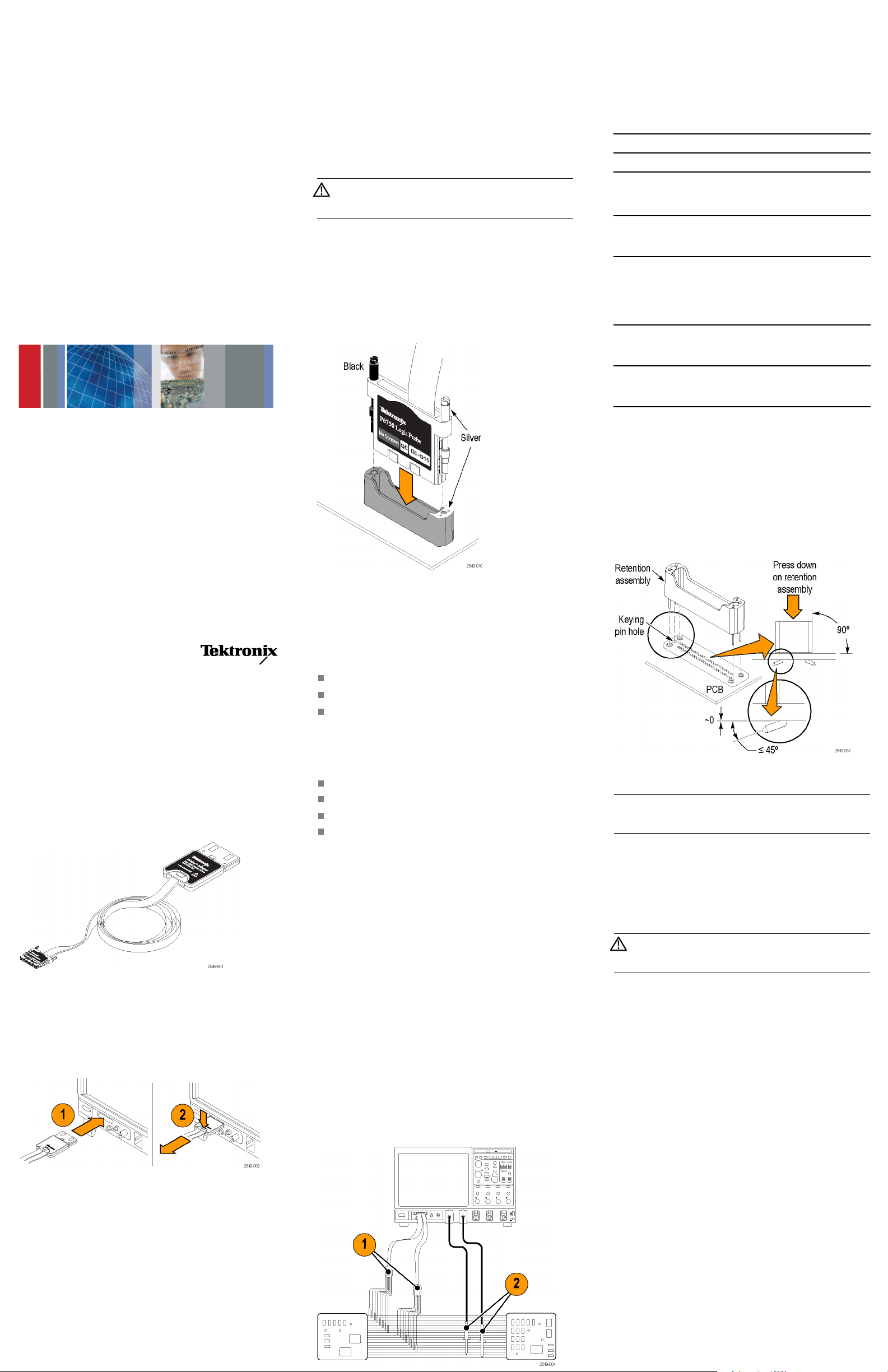
Installing the Probe Retention Assembly
The probe retention assembly provides a housing around the
connector footprint to secure the probe to the PCB. To install the
probe retention assembly on the circuit board, do the following:
1. If your PCB has multiple connector footprints, locate the
correct one.
2. Align the retention assembly over the footprint so that the
keying pin on the retention assembly lines up with the
keying pin hole on the footprint.
1
*P0712
071-2849-00
84900*
Product Description
The P6750 logic probe is a 17-channel, high-density
connectorless probe with D-Max probing technology. It
connects the 16 digital channels on Tektronix MSO70000
Series oscilloscopes to digital buses and signals on your target
system. A clock/qualifier (QC) input is also provided.
The cLGA contact (compression Land Grid Array) on the probe
mates to a PCB footprint that you design into your system
circuit board. The probe is secured with two thumbscrew s to a
retention assembly that you solder onto the circuit board.
2. Start both screws in the retention assembly, and tighte
them evenly to ensure that the probe approaches and mates
squarely to the PCB. The probe is completely fastened to
the PCB w hen the screws stop in the assembly.
Setting Up the Probe
From the Digital menu, select Digital Setup to set and view the
following parameters of each digital channel:
Threshold voltage and vertical position
Signal height
Channel label
The default settings are 1.4 V t hresholds with digital channel
number labels.
From the Digital menu, select Bus Setup to set and view bus
characteristics such as:
Clock source
Bus type (Serial or Parallel)
Bus width
Display format (Hex, Binary, or ASCII symbols)
Parallel bus setup information is resident on MSO70000 Series
oscilloscopes. However, for other buses such as I2C, you must
have the a ppropriate option. See your oscilloscope manual or
product data sheet for nomenclature and ordering details.
(set once for all 16 channels)
n
3. Insert the retention assembly into the holes in the footprint
on the PCB.
NOTE. The following two steps are important to ensure that
the retention assembly is correctly m ounted and that the probe
makes proper contact with the PCB.
4. Hold the retention assembly so that it is firmly flush with
the surface of the PCB, and the four anchoring posts
extend through the circuit board to the opposite side.
5. Using a pair of needle-nose pliers, hold one of the posts.
Using the circuit board hole as a fulcrum, bend the post
outwardsothatitisflush with the PCB surface, anchoring
the assembly to the PCB. Bend the other three posts in
the same manner.
CAUTION. After you insert the wires in the board, it is
important to bend the anchoring posts out to avoid solder
creep.
Connecting the Probe to the Oscilloscope
Connect the probe as shown in the illustration below.
1. Insert the probe label-side up into the receptacle.
2. To remove the probe, push the probe in, press the button,
ull out the probe.
and p
Functional Che ck
Logic activity immediately displays on all connected, active
channels. If you do not see an active signal:
1. Press Trigger.
2. Select Edge for trigger type.
3. Select the channel that you are setting up as the source.
If you still do not see a n active signal, use an analog probe or the
iCapture analog mu
x to verify circuit activity at the test point.
Typical Application
1. Use the P6750 probe to view digital signals on a data bus.
2. Use iCapture or analog probes, such as the P7508 TriMode
probe to view analog waveform information.
6. Solder the anchoring posts to the PCB.
x
Specifications
Table 1: E lectrical and mechanical specifications
Characteristic Description
Input channels
Bandwidth
Slew rate limit 6 V/ns for signals <2 Vpk-pk
Maximum nondestructive
al to probe
input sign
Input resistance
Input capacitance 3.0 pF, probe only
Probe length
16 data, 1 clock/qualifier
1.0 GHz
±15 V
20 kΩ ±2.0%
1.0m(3.28ft)
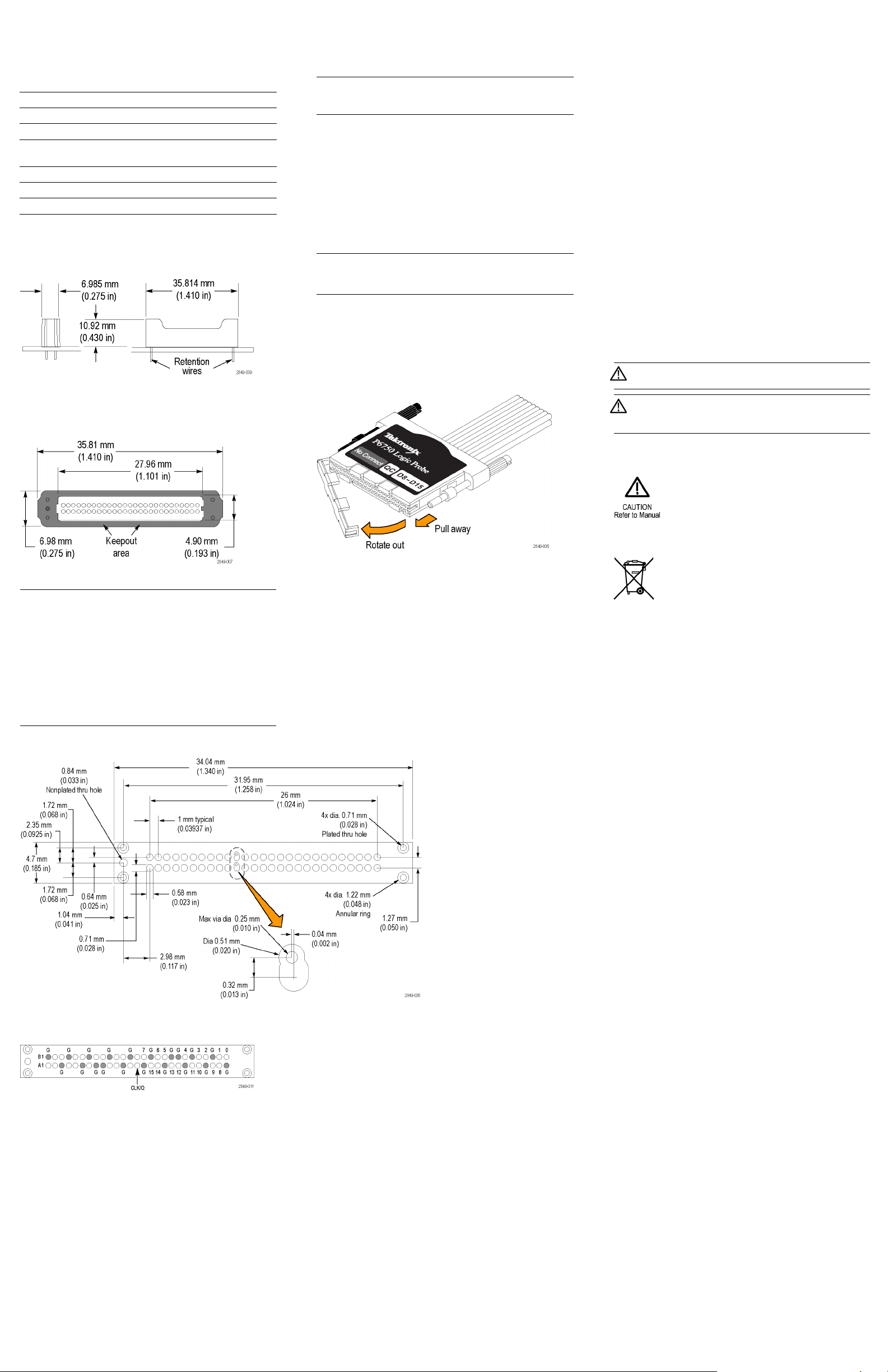
Dimensions
All dimensions are per standard IPC tolerance (±0.004 in).
Vias must be placed outside the keepout area. Any traces routed
on the top layer of the board must stay outside the keepout area.
Traces may be routed on inner layers of the board through the
keepout area.
Table 2: Environmental specifications
Characteristics Description
Temperature
Operating
Nonoperating
Humidity
Operating
Nonoperating
Altitude
Operating
Nonoperating
Replacing
the Probe Head Contacts
0 °C (+32 °F) to +50 °C (+122 °F)
–55 °C to +75 °C (–67 °F to +167 °F)
5% to 95% relative humidity at up to
+30 °C (+86 °F)
5% to 75% RH above +30 °C
(+86°F)upto+50°C(+122°F),
noncondensing
5% to 95% relative humidity at up to
+30 °C (+86 °F)
5% to 75% RH above +30 °C
(+86 °F) up
noncondensing
3 km (9,843 ft) maximum
4.6 km (15,
to +60 °C (+140 °F),
092 ft) maximum
To replace the contacts, do the following:
1. Gently pull one side of the contacts away from the probe
head as shown, and then remove the entire clip.
Safety Sum m ary
Connect and Disconnect Properly. Connect the probe output
to the measurement instrument before connecting the probe
to the circuit under test. Disconnect the probe input and the
probe ground from the circuit under test before disconnecting
the probe from the measurement instrument.
Observe All Terminal Ratings. To avoid fire or shock hazard,
observe all ratings and markings on the product. Consult the
product manual for further ratings information before making
connections to the product.
Do not Operate Without Covers. Do not touch exposed
connections and components when power is present.
Avoid Exposed Circuitry. Do not touch exposed connections
and components when power is present.
Do Not Operate With Suspected Failures. If you suspect there is
damage to this product, have it inspected by qualified service
personnel.
Do Not Operate in Wet/Damp Conditions. Do Not Operate in an
Explosive Atmosphere.
Keep Product Surfaces Clean and Dry.
Safety Terms and Symbols in This Manual.
These terms may appear in this manual:
WARNING. Warning statements identify conditions or
practices that could result in injury or loss of life.
CAUTION. Caution statements identify conditions or
practices that could result in damage to this product or
other property.
NOTE. Y
ou should use immersion gold surface finish for the
best performance. Also, let the probe attachment holes float
in unconnected to a ground plane. This prevents
or rema
overheating the ground plane and promotes quicker soldering
etention posts to your PCB.
of the r
Use via-in-pad to route signals to the pads on the circuit board.
This allows you to minimize the stub length of the signals
on your board, thus providing the smallest intrusion to your
signals. It also enables you to minimize the board area that is
used for the probe footprint and maintain the best electrical
performance of your design.
2. Align the new contact clip with the probe head and gently
snap it into place.
3. Test the probe to confirm that all channels are functional.
Symbols on the Product. This symbol may appear on the
product:
Equipmen
with the European Union’s requirements according
to Directive 2002/96/EC on waste electrical
and electronic equipment (WEEE). For more
information about recycling options, check the
Support/Service section of the Tektronix Web site
(www.tek
t Recycling. This product complies
tronix.com).
Contacting Tektronix
Web site: www.tekt
Phone: 1-800-833-9200
Address: Tektronix, Inc.
Email:
ronix.com
Department or name (if known)
14200 SW Karl Braun
Drive P.O. Box 500
on, OR 97077
Beavert
USA
techsupport@tektronix.com
Probe Footprint P inout
The mating signal layout for your circuit board is shown below.
Warranty Information
For warranty information, go to www.tektronix.com/warranty.
Copyright © Tektronix, Inc. All rights reserved. www.tektronix.com
xx
P6750 型
汎用ロジック・プローブ
取扱説明書
プローブと測定回路の接続
プローブを接続できるのは、プローブと一致する圧縮フット
プリントを有する被測定システムと、はんだ付けされたプロー
ブ・リテンション・アセンブリのみです(詳細については「寸法」
と「プローブ・リテンション・アセンブリの取り付け」を参照して
ください)。なお、プローブを接続する前に、フットプリント・コ
ンタクトのクリーニングを行う必要があります。
圧縮フットプリントのクリーニング
プローブを被測定システムに接続する前に、回路基板の圧
縮フットプリントのクリーニングを行う必要があります。
注意: なお、感電および機器の損傷を防ぐため、圧縮
フットプリントのクリーニングは、必ず被測定システムの電
源をオフにした状態で行ってください。
1. リント(離脱繊維)の出ないクリーンルーム専用クロスに電
子機器用のイソプロピル・アルコールを若干湿らせて、
フットプリント面を軽く拭き取ります。
2. リントが付着している場合は、窒素エアガンまたは油分
を含まない清浄な乾燥空気で吹き飛ばします。
プローブの接続
1. プローブの銀色のネジをリテンション・アセンブリの銀色
のサイドに合わせます。
プローブの保管
不使用時は、プローブ・ヘッドに慎重にプローブ・カバーを
かぶせて保管し、プローブ・ヘッド・コンタクトを保護してくだ
さい。
スタンダード・アクセサリ
説明 部品番号
プローブ・カバー、帯電防止材付き 200-4893-XX
P6750 型ロジック・プローブ指示書 071-2849-XX
オプショナル・アクセサリ
説明 用途 部品番号
コンタクト・ア
センブリ
プローブ・リ
テンション・
アセンブリ
デスキュー・
フィクスチャ
スクエア・ピ
ン・アダプタ
磨滅または損傷したプロー
ブ・ヘッド・コンタクトの補修に
使用します
プローブと回路基板の接続
に使用します
2個口
50個口
デジタル・プローブ・チャンネ
ルのトリガ・パスの調整に使用
します
プローブのフットプリントとス
クエア・ピン・ヘッダの接続に
使用します
020-2622-XX
020-2908-XX
020-2910-XX
067-2083-XX
NEX-P6960PIN
2
49-00
071-28
製品の説明
P6750 型ロジック・プローブは、17 チャンネルの高密度 D-Max
コネクタレス・プローブです。これを使用して、当社 MSO70000
シリーズ・オシロスコープの 16 デジタル・チャンネルと被測定
システムのデジタル・バスおよび信号を接続することができま
す。クロック/クオリファイア(QC)入力もあります。
プローブの cLGA (compression Land Grid Array)コン タクト
は、システム回路基板の PCB フットプリントに接続します。プ
ローブは、回路基板にはんだ付けしたリテンション・アセンブ
リに 2 本のサムネジで固定します。
プローブとオシロスコープの接続
下の図に示すようにプローブを接続します。
1. ラベル面を上にしてプローブをレセプタクルに挿入しま
す。
2. 取り外す
解除ボタンを押して引き抜きます。
場合は、プローブをいったん押し込み、ロック
2. 2 本あるネジの両方を回してプローブをリテンション・ア
センブリに正しく接続し、均等の力で締めて PCB に固
定させます。ネジがアセンブリのネジ穴の中で回らなく
なれば、プローブは PCB に完全に固定されています。
プローブのセットアップ
Digital メニューから Digital Setup を選択して、各チャンネル
の下記パラメータを表示または設定します。
スレッショルド電圧と垂直軸位置
信号高さ(全 16 チャンネルを一括設定)
チャンネル・ラベル
デフォルト設定は
、スレッショルド電圧 1.4 V、デジタル・チャ
ンネル番号ラベルとなっています。
Digital メニューから Bus Setup を選択して、以下のバス特性
を設定または表示します。
クロック・ソース
バスの種類(シリアルまたはパラレル)
バス幅
表示形式(16 進、2 進、または ASCII シンボル)
パラレル・ バスの設定情報は MSO70000 シリーズ・オシロス
コープに保存されています。しかし I2C など、その他のバス
については適切なオプションが必要です。名称と発注情報
については、ご使用のオシロスコープのマニュアルまたは製
品データ・シートを参照してください。
機能チェック
接続されたすべてのアクティブなチャンネルについて、ロジッ
ク動作が直ちに表示されます。アクティブな信号が表示され
ない場合は、次の操作を行ってください。
1. Trigger を押します。
2. トリガのタイプとして Edge を選択します。
3. ソースとしてセットアップするチャンネルを選択します。
それでもアクティブな信号が表示されない場合は、アナログ・
プローブまたは iCapture アナログ・マルチプレクスを使用し
て、測定ポイントにおける回路の挙動を検証してください。
主な用途
1. P6750 型プローブは、データ・バスのデジタル信号の観
測に使用します。
2. iCapture またはアナログ・プ ロー ブ(P7508 型 TriMode
プローブなど)を使用してアナログ波形情報を観測しま
す。
プローブ・リテンション・アセンブリの取り付け
プローブ・リテンション・アセンブリは
、プローブのコネクタ・フッ
トプリントを PCB に固定するためのハウジングです。プロー
ブ・リテンション・アセンブリを回路基
板に取り付けるには、以
下の手順に従います。
1. PCB に複数のコネクタ・フットプリントがある場合は、プ
ローブに合うフットプリントを特定します。
2. リテンション・アセンブリの固定ピンがフットプリントのピ
ン穴に収まるよう、リテンション・アセンブリをフットプリン
トの上に置きます。
3. PCB のフットプリントのピン穴にリテンション・アセンブリ
の固定ピンを挿入します。
注: 次の 2 つの手順でリテンション・アセンブリを取り付け、
プローブを PCB に接続します。この 2 つは特に細心の注意
を払って実行してください。
4. リテンション・アセンブリを PCB の表面に密着させ、4 本
のアンカー・ポストが回路基板の穴を通って反対側に出
るようにします。
5. ニードルノーズ・プライヤーでポストのうちの 1 本をつま
み、回路基板の穴を支点としてポストを外側に向けて折
り曲げ、アセンブリが PCB の表面に密着するようにして
固定します。残る 3 本のポストも同様に折り曲げます。
注意: 基板にリテンション・ワイヤを通した後、アンカー・
ポストを外側に向けて折り曲げるのは、はんだのクリープ
現象を防止するための重要な措置です。
6. アンカー・ポストを PCB にはんだ付けします。
x
 Loading...