

Page 1

xx
P6700 Series
ZZZ
Serial Analyzer Probes
Instruction Manual
*P077011500*
077-0115-00
Page 2

Page 3

xx
P6700 Series
ZZZ
Serial Analyzer Probes
Instruction Manual
Revision B
www.tektronix.com
077-0115-00
Page 4

Copyright © Tektronix. All rights reserved. Licensed software products are owned by Tektronix or its subsidiaries
or suppliers, and are protected by national copyright laws and international treaty provisions.
Tektronix products are c overed by U.S. and foreign patents, issued and pending. Information in this publication
supersedes that in all previously published material. Specifications and price change privileges reserved.
TEKTRONIX and TEK are registered trademarks of Tektronix, Inc.
RT-Eye is a registered trademark of Tektronix, Inc.
PCI Express is a registered trademark of PCI-SIG®.
G3PO is a trademark of Corning Gilbert Inc.
Contacting Tektronix
Tektroni
14200 SW Karl Braun Drive
P.O . Bo x 50 0
Beaverton, OR 97077
USA
For pro
x, Inc.
duct information, sales, service, and t echnical support:
In North America, call 1-800-833-9200.
Worl d wide, vi sit www.tektronix.com to find contacts in your area.
Page 5

Warranty
Tektronix warrants that this product will be free from defects in materials and workmanship for a period of one (1)
year from the date of shipment. If any such product proves defective during this warranty period, Tektronix, at its
option, either will repair the defective product without charge for parts and labor, or will provide a replacement
in exchange for the defective product. Parts, modules and replacement products used by Tektronix for warranty
work may be n
the property of Tektronix.
ew or reconditioned to like new performance. All replaced parts, modules and products become
In order to o
the warranty period and make suitable arrangements for the performance of service. Customer shall be responsible
for packaging and shipping the defective product to the service center designated by Tektronix, with shipping
charges prepaid. Tektronix shall pay for the return of the product to Customer if the shipment is to a location within
the country in which the Tektronix service center is located. Customer shall be responsible for paying all shipping
charges, duties, taxes, and any other charges for products returned to any other locations.
This warranty shall not apply to any defect, failure or damage caused by improper use or improper or inadequate
maintenance and care. Tektronix shall not be obligated to furnish service under this warranty a) to repair damage
result
b) to repair damage resulting from improper use or connection to incompatible equipment; c) to repair any damage
or malfunction caused by the use of non-Tektronix supplies; or d) to service a product that has been modified or
integrated with other products when the effect of such modification or integration increases the time or difficulty
of servicing the product.
THIS WARRANTY IS GIVEN BY TEKTRONIX WITH RESPECT TO THE PRODUCT IN LIEU OF ANY
OTHER WARRANTIES, EXPRESS OR IMPLIED. TEKTRONIX AND ITS VENDORS DISCLAIM ANY
IMPLIED WARRANTIES OF MERCHANTABILITY OR FITNESS FOR A PARTICULAR PURPOSE.
TRONIX’ RESPONSIBILITY TO REPAIR OR REPLACE DEFECTIVE PRODUCTS IS THE SOLE
TEK
AND EXCLUSIVE REMEDY PROVIDED TO THE CUSTOMER FOR BREACH OF THIS WARRANTY.
TEKTRONIX AND ITS VENDORS WILL NOT BE LIABLE FOR ANY INDIRECT, SPECIAL, INCIDENTAL,
OR CONSEQUENTIAL DAMAGES IRRESPECTIVE OF WHETHER TEKTRONIX OR THE VENDOR HAS
ADVANCE NOTICE OF THE POSSIBILITY OF SUCH DAMAGES.
[W2 – 15AUG04]
btain service under this warranty, Customer must notify Tektronix of the defect before the expiration of
ing from attempts by personnel other than Tektronix representatives to install, repair or service the product;
Page 6

Page 7

Table of Contents
General Safety Summary .......................................................................................... v
Service Safety Summary........................ ................................ ................................ . vii
Environmental Considerations .................................................................................. viii
Preface.............................................................................................................. ix
Related Documentation ...................................................................................... ix
List of Terms ................................................................................................... x
Getting Started . . . .. . ... ... . .. . ... ... . ... ... . . .. . ... ... . ... ... ... . ... ... . ... ... ... . ... ... . .. . ... ... . ... ... ... . ... ... . 1
Product Description....................................... ................................ ..................... 1
Serial Analyzer Configurations........................ .................................. ..................... 4
Operating Basics.................................................................................................... 5
Preparing for Installation of the Midbus Retention Mechanism.......................................... 5
Installing the Midbus Retention Mechanism . ... . ... ... ... . ... ... . .. . ... ... . ... ... ... . ... ... . ... ... ... . ... . 5
Connecting the Midbus Probe..... ................................ .................................. ......... 7
Arranging the Midbus Probe Cables......................................................................... 9
Connecting a Slot Interposer Probe......................................................................... 10
Connecting the Solder-Down Probe ................ ................................ ........................ 14
Reference ................... .................................. ................................ ...................... 19
Probe Dimensions ............................................................................................ 19
Circuit Board Design......................................................................................... 23
Midbus Footprint Pin and Probe Channel Assignments........ ................................ .......... 40
Rearranging Wires in the Probe Connector ................................................................ 57
Adding Probes to the P6701SD Probe Connector........................... .............................. 60
Specifications .... .................................. ................................ ................................ 61
Environmental. ................................ .................................. .............................. 61
Maintenance........................................................................................................ 63
Inspection and Cleaning.......................................... ................................ ............ 67
Storing the Probe.................................... .................................. ........................ 67
Repackaging Instructions ...... ................................ .................................. ............ 67
Appendix A: PCI Express System Design Review Checklist ................................................ 69
General Consideratio
Midbus Probe Configuration ................................................................................ 69
Mechanical Considerations .......... .................................. ................................ ...... 69
Electrical Considerations .... ................................ .................................. .............. 71
Appendix B: Reference Files................................... ................................ .................. 73
Index
ns .... .................................. ................................ ................ 69
P6700 Series Serial Analyzer Probes Instruction Manual i
Page 8

Table of Contents
List of Figure
Figure 1: P6716 16-Channel Midbus probe .............. ................................ ....................... 1
Figure 2: P6708S Slot interposer probe.......................................................................... 2
Figure 3: P6701SD Solder-Down probe ......................................................................... 3
Figure 4: 16-Channel footprint..................................... ................................ ............... 5
Figure 5: Installing the retention mechanism. . ... ... . .. . ... ... . ... ... ... . ... ... . . .. . ... ... . .. . ... ... . .. . ... ... . . 6
Figure 6: Soldering the anchoring posts to the PCB............................................................ 6
Figure 7: Connecting a probe to the retention mechanism.................................... ................. 8
Figure 8: Arranging the midbus probe cables ................................................................... 9
Figure 9: Connecting a slot interposer probe......... ................................ .......................... 11
Figure 10: Installing the P6701SD probe ... ... . .. . ... ... . ... ... . ... ... . .. . ... ... . ... ... . ... ... . .. . ... ... . ... ... 14
Figure 11: Connecting the P75TLRST tip to the probe head................................................. 15
Figure 12: Connecting wires to the circuit.......... ................................ ............................ 16
Figure 13: Connecting the tip to the circuit............... ................................ ...................... 17
Figure 14: P6716S dimensions................................... ................................ ................ 19
Figure 15: P6716 cable length dimensions ..................................................................... 20
Figure 16: P6716S cable length dimensions...... ................................ .............................. 20
Figure 17: P6701S, P6704S, and P6708S dimensions .............. ................................ .......... 21
Figure 18: P6701SD dimensions ............ ................................ .................................. .. 22
Figure 19: P75TLRST Solder Tip dimensions................................................................. 22
Figure 20: 8-Channel midbus footprint dimensions and keep-out area ..................................... 24
Figure 21: 16-Channel midbus footprint dimensions and keep-out area .................................... 25
Figure 22: Recommended trace routing on primary surface layer ............. .............................. 26
Figure 23: Via and trace keep-out areas for the P6708 8-Channel probe ................................... 27
Figure 24: Via and trace keep-out areas for the P6716 16-Channel probe ................ .................. 27
Figure 25: Recomme nded trace routing on inner or secondary surface layer (prima
shown) ......................................................................................................... 27
Figure 26: Recommended trace routing on inner or secondary surface layer (primary layer pads not
shown) ......................................................................................................... 28
Figure 27: Clock cable connector dimensions ................................................................. 29
Figure 28: P75TLRST TriMode Long Reach Solder Tip ..................................................... 30
Figure 29: Typical wire length from probe tip to circuit...................................................... 31
Figure 30: P75TLRST solder tip with 0.010 inch of tip wire ................................ ................ 32
Figure 31: P75TLRST solder tip with 0.050 inch of tip wire ................................ ................ 32
Figure 32: P75TLRST solder tip with 0.100 inch of tip wire ................................ ................ 33
Figure 33: P75TLRST solder tip with 0.200 inch of tip wire ................................ ................ 33
Figure 34: P75TLRST TriMode Long Reach Solder Tip dimensions ....................................... 34
Figure 35: Signal eye measurements (time versus voltage) .................................................. 34
Figure 36: Periodic jitter gain function ... ... ... . ... ... ... . ... ... ... . ... ... . .. . ... ... . .. . ... ... . ... ... ... . ... ... 36
s
ry layer pads
ii P6700 Series Serial Analyzer Probes Instruction Manual
Page 9

Table of Contents
Figure 37: S-pa
Figure 38: S-parameter data of retention mechanism plus P6700 Series midbus probe................... 37
Figure 39: S-parameter data of P6701SD Solder-Down probe................................... ............ 38
Figure 40: Slot Interposer probe with a clock cable connected .. .................................. .......... 39
Figure 41: P6708 8-Channel probe footprint pin assignments ............................................... 40
Figure 42: P6716 16-Channel probe footprint pin assignments.............................................. 40
Figure 43: 8
Figure 44: 16-Channel midbus footprint connection module connector .................................... 41
Figure 45: Opening the probe connector........................................................................ 58
Figure 46: Removing the probe sleeve.......................................................................... 58
Figure 47: Probe labels ........................................................................................... 59
Figure 48: Removing individual wires.......................................................................... 59
Figure 4
Figure 50: Replaceable bullets and tool... ................................ ................................ ...... 63
Figure 51: Removing the bullet contacts ... .................................. ................................ .. 64
Figure 52: Inspect the bullet contacts ........................................................................... 65
Figure 53: Installing the bullet contacts. ... . .. . ... ... . .. . ... ... . .. . ... ... . ... ... ... . ... ... ... . ... ... ... . ... ... .. 66
9: Inserting additional probe wires . ... ... ... . .. . ... ... ... . ... ... ... . .. . ... ... . .. . ... ... ... . ... ... ... . . 60
rameter data of retention mechanism only ................................................... 37
-Channel midbus footprint connection module connector...................................... 40
P6700 Series Serial Analyzer Probes Instruction Manual iii
Page 10

Table of Contents
List of Tables
Table i: Terms used in this document ............................................................................ x
Table 1: Ser
Table 2: Recommended circuit board design criteria.......................................................... 23
Table 3: Via and trace characteristics ....... ................................ .................................. .. 26
Table 4: Clock cable three-pin connector pin assignments ................................................... 28
Table 5: Probe Eye Requirements ............... .................................. .............................. 35
Table 6: Reference clock electrical requirements .............................................................. 39
Table 7: X
Table 8: X8 bidirectional link.................................................................................... 44
Table 9: X8 (2) unidirectional links ............................................................................. 45
Table 10: X4 bidirectional link .................................................................................. 46
Table 11: X4 (2) unidirectional links................................ ................................ ............ 47
Table 12: X2 bidirectional link .................................................................................. 48
Table
Table 14: X1 bidirectional link .................................................................................. 50
Table 15: X1 (2) unidirectional links.......................... ................................ .................. 51
Table 16: X8 unidirectional link ............................. ................................ .................... 52
Table 17: X4 bidirectional link .................................................................................. 52
Table 18: X4 (2) unidirectional links.......................... ................................ .................. 53
ble 19: X4 unidirectional link and a X2 unidirectional link ................... ............................ 53
Ta
Table 20: X4 unidirectional link and a X1 unidirectional link . .................................. ............ 54
Table 21: X2 bidirectional link .................................................................................. 54
Table 22: X2 (2) unidirectional links.......................... ................................ .................. 55
Table 23: X1 bidirectional link .................................................................................. 55
Table 24: X1 (2) unidirectional links.......................... ................................ .................. 56
Table 25: Atmospheric characteristics .......................................................................... 61
Table 26: Midbus Probe Configuration ..... .................................. ................................ .. 69
Table 27: Midbus Probe .......................................................................................... 69
Table 28: Slot Interposer Probe .................................................................................. 70
Table 29: Reference Clock Connector .............................. .................................. .......... 70
Table 30: Midbus Probe .......................................................................................... 71
Table 31: Slot Interposer Probe .................................................................................. 71
Table 32: Reference Clock Connector .............................. .................................. .......... 72
ial analyzer configuration............................. ................................ ............... 4
16 unidirectional link ................. .................................. .............................. 43
13: X2 (2) unidirectional links............................................ ................................ 49
iv P6700 Series Serial Analyzer Probes Instruction Manual
Page 11

General Safety Summary
General Safet
To Avoid Fire or Personal
Injury
ySummary
Review the fo
this product or any products connected to it.
To avoid pot
Only qualified personnel should perform service procedures.
While using this product, you may need to access other parts of a larger system.
Read the safety sections of the other component manuals for warnings and
cautions r
Connect and Disconnect Properly. Connect the probe output to the measurement
instrument before connecting the probe to the circuit under test. Connect the
probe reference lead to the circuit under test before connecting the probe input.
Disconnect the probe input and the probe reference lead from the circuit under test
before
Ground the Product. This product is indirectly grounded through the grounding
condu
conductor must be connected to earth ground. Before making connections to
the input or output terminals of the product, ensure that the product is properly
grounded.
disconnecting the probe from the measurement instrument.
ctor of the mainframe power cord. To avoid electric shock, the grounding
llowing safety precautions to avoid injury and prevent damage to
ential hazards, use this product only as specified.
elated to operating the system.
Observe All Terminal Ratings. To a v o i d fire or shock hazard, observe all ratings
and markings on the product. Consult the product manual for further ratings
information before making connections to the product.
The inputs are not rated for connection to mains or Category II, III, or IV circuits.
Do not apply a potential to any terminal, including the common terminal, that
exceeds the maximum rating of that terminal.
Power Disconnect. The power cord disconnects the product from the power source.
Do not block the power cord; it must remain accessible to the user at all times.
Do Not Operate Without Covers. Do not operate this product with covers or panels
removed.
Do Not Operate With Suspected Failures. If you suspect that there is damage to this
product, have it inspected by qualified service personnel.
Avoid Exposed Circuitry. Do not touch exposed connections and components
when power is present.
P6700 Series Serial Analyzer Probes Instruction Manual v
Page 12
General Safety Summary
TermsinthisManual
Symbols and Terms on the
Product
Do Not Operate i
Do Not Operate in an Explosive Atmosphere.
Keep Product Surfaces Clean and Dry.
Provide Prop
details on installing the product so it has proper ventilation.
These terms may appear in this manual:
WARNING.
in injury or loss of life.
CAUTION
damage to this product or other property.
These t
. Caution statements identify conditions or practices that could result in
erms may appear on the product:
DANGER indicates an injury hazard immediately accessible as you read
the ma
n Wet/Damp Conditions.
er Ventilation. Refer to the manual’s installation instructions for
Warning statements identify conditions or practices that could result
rking.
WARNING indicates an injury hazard not immediately accessible as you
the marking.
read
CAUTION indicates a hazard to property including the product.
The following symbol(s) may appear on the product:
vi P6700 Series Serial Analyzer Probes Instruction Manual
Page 13

Service Safety Summary
Service Safet
y Summary
Only qualifie
Safety Summary and the General Safety Summary before performing any service
procedures.
Do Not Service Alone. Do not perform internal service or adjustments of this
product unless another person capable of rendering first aid and resuscitation is
present.
Disconnect Power. To avoid electric shock, switch off the instrument power, then
disconnect the power cord from the mains power.
UseCareWhenServicingWithPowerOn. Dangerousvoltagesorcurrentsmay
exist in
disconnect test leads before removing protective panels, soldering, or replacing
components.
To avoid electric shock, do not touch exposed connections.
d personnel should perform service procedures. Read this Service
this product. Disconnect power, remove battery (if applicable), and
P6700 Series Serial Analyzer Probes Instruction Manual vii
Page 14
Environmental Considerations
Environmenta
Product End-of-Life
Handling
Restriction of Hazardous
Substances
l Considerations
This section
Observe the following guidelines when recycling an instrument or component:
Equipment R
use of natural resources. The equipment may contain substances that could be
harmful to the environment or human health if improperly handled at the product’s
end of life. In order to avoid release of such substances into the environment and
to reduce the use of natural resources, we encourage you to recycle this product
in an appropriate system that will ensure that most of the materials are reused or
recycle
This product has been classified as Monitoring and Control equipment, and is
outside the scope of the 2002/95/EC RoHS Directive.
provides information about the environmental impact of the product.
ecycling. Production of this equipment required the extraction and
d appropriately.
This symbol indicates that this product complies with the European Union’s
requirements according to Directive 2002/96/EC on waste electrical and
nic equipment (WEEE). For information about recycling options, check
electro
the S upport/Service section of the Tektronix Web site (www.tektronix.com).
viii P6700 Series Serial Analyzer Probes Instruction Manual
Page 15

Preface
Preface
This manual c
ontains information needed to install and use a P6700 Series probe
with a TLA7S08 or TLA7S16 Serial Analyzer module to debug, validate, and
verify computer and embedded systems.
Related Documentation
The following table lists related documentation available for your instrument. The
documentation is available on the TLA Documentation CD and on the Tektronix
Web site (www.Tektronix.com/manuals).
For documentation not specified in the table, contact your local Tektronix
representative.
Related Documentation
Item Purpose Location
TLA Quick Start User Manuals
eHelp
Onlin
Installation Quick Reference Cards High-level installation information
High-level operational overview
In-depth operation and UI help
Installation Manuals
XYZs of Logic Analyzers
Declassification and Securities
tructions
ins
Application notes
Product Specifications & Performance
Verification Procedures
TPI.NET Documentation
iled first-tim e installation information
Deta
Logic analyzer basics
Data security concerns specificto
itizing or removing m emory devices
san
from Te ktronix products
Collection of logic analyzer application
specific notes
TLA Product specifications and
performance verification procedures
Detailed information for controlling the
logic analyzer using .NET
P6700 Series Serial Analyzer Probes Instruction Manual ix
Page 16
Preface
Related Documentation (cont.)
Item Purpose Location
Field upgrade kits
Optional Service Manuals Self-service documentation for modules
Upgrade information for your logic
analyzer
and mainfr
ames
List of Terms
The following is a list of terms that appear in this manual. You may want to
review this list if you are unfamiliar with some of the terms. For a list of PCI
Express®-specific terms, refer to the PCI Express Base Specification.
Table i: Terms used in this document
Term Description
Footprint
tion Mechanism
Reten
Probe Head
Full-width
Half-width 8-Channel
Link
Differential Pair A set of two signals, positive and negative, transmitting data
Lane
PCB
SUT System under test. This is the system/circuit board(s) you intend
An arrangement of pads built into the board as specified in the
PCI Exp
retention mechanism.
The mechanism that connects the probe head to the PCB. It fits
on the footprint and must be soldered to the PCB.
The end of the probe that connects to the retention mechanism.
16-Channel
A connection between two PCI Express devices. A link consists
of
of a number (N) lanes.
from one device to another.
A single differential pair (two signals) that transmit data in one
d
Printed circuit board
to test with the serial analyzer.
ress Base Specification. It is the contact point for the
a number of lanes. A link described as by-N (or xN) consists
irection of a PCI Express Link. A unidirectional lane.
x P6700 Series Serial Analyzer Probes Instruction Manual
Page 17
Getting Started
Product Descr
Midbus Probes
iption
Tektronix offers three types of probes for the TLA7S08 and TLA7S16 Serial
Analyzer modules:
Midbus probes
Slot interposer probes
Solder-down probes
A midbus p
You must install the retention mechanism to either a PCI Express Gen1 or Gen2
footprint on your circuit board.
Tektronix offers the following midbus probes:
P6708 8
P6716 16-Channel Midbus probe
robe connects to a retention mechanism installed on your circuit board.
-Channel Midbus probe
Figure 1: P6716 16-Channel Midbus probe
P6700 Series Serial Analyzer Probes Instruction Manual 1
Page 18

Getting Started
Slot Interposer Probes
A slot interpos
has a x16 connector for a PCI Express card device.
Tektronix off
P6701S PCI Express x1 Slot Interposer probe
P6704S PCI Express x4 Slot Interposer probe
P6708S PCI Express x8 Slot Interposer probe
P6716S PCI Express x16 Slot Interposer probe
er probe connects to a PCI Express slot on your SUT. Each probe
ers the following (bidirectional) slot interposer probes:
Figure 2: P6708S Slot interposer probe
2 P6700 Series Serial Analyzer Probes Instruction Manual
Page 19

Getting Started
P6701SD Solder-Down
Probe
The P6701SD pro
tip (P75TLRST). Up to four probes (one differential pair each) can be installed in
each signal connector to the serial module. (See page 60, Adding Probes to the
P6701SD Probe Connector.)
be connects to your SUT through the differential solder-down
Figure 3: P6701SD Solder-Down probe
P6700 Series Serial Analyzer Probes Instruction Manual 3
Page 20

Getting Started
Serial Analyz
er Configurations
The following table lists the minimum serial analyzer configuration required by
link widths.
Table 1: Ser
Link width
X11111
X41111
X81112
X16 1 2 2 2
1
The link width can be supported with either a P6716P Slot Interposer probe or a P6708 Slot Interposer probe.
Choose one or the other, based on the footprint on your platform.
To capture signals from a bidirectional X16 link, you will need two serial analyzer
modules connected to a slot interposer probe. (See page 12, Connecting a Probe
to a Bidirectional X16 Link.)
ial analyzer configuration
TLA7S16
TLA7012
or TLA7016
mainframe
Serial
Analyzer
module P6716 probe
1
P6708 probe
1
4 P6700 Series Serial Analyzer Probes Instruction Manual
Page 21
Operating Basics
Preparing for Installation of the Midbus Retention Mechanism
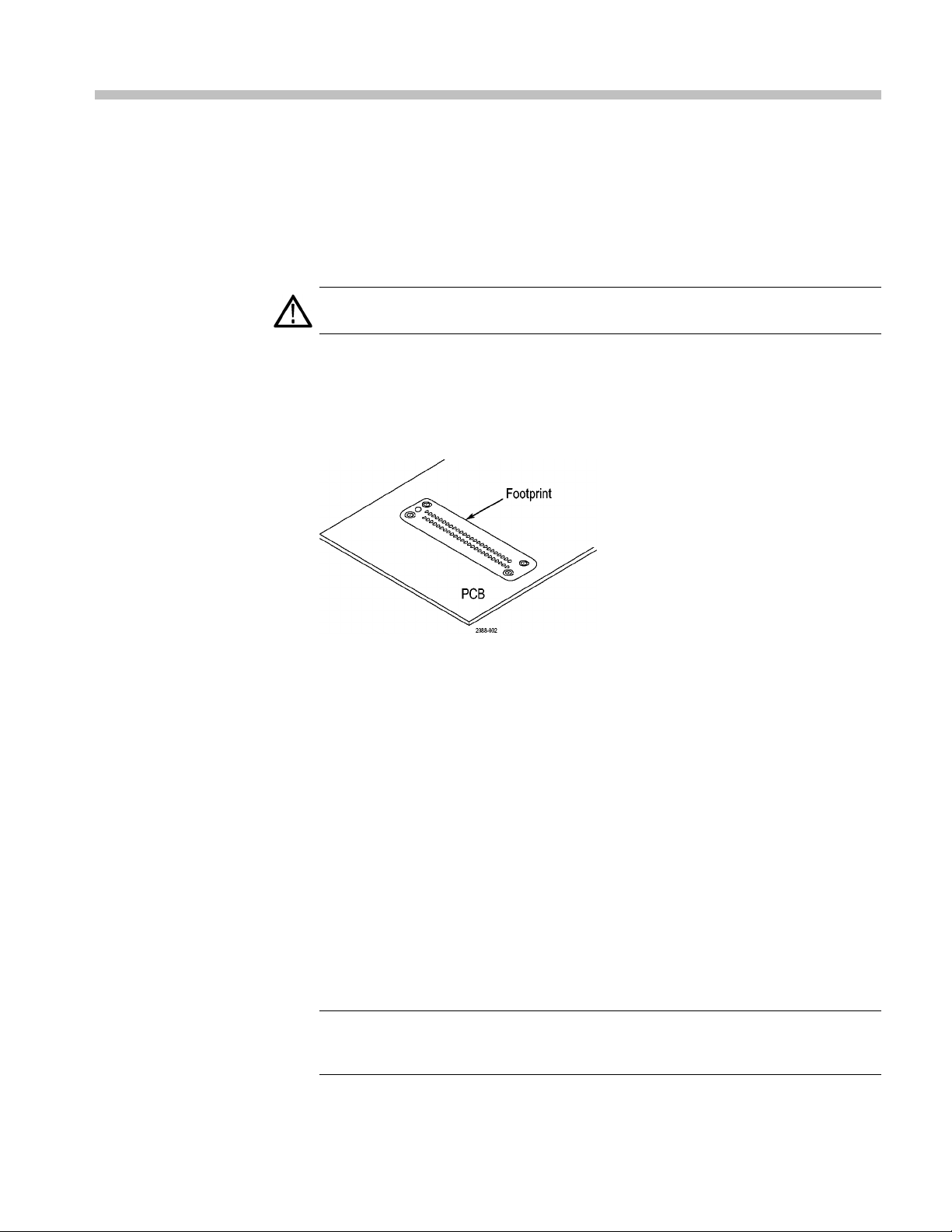
Cleaning the Footprint
Inspect the footprint for lint, oil, or fingerprints. If the footprint is dirty, clean it by
following these steps:
CAUTION. To avoid electrical damage, always power off your system under test
before cleaning the footprint.
1. Use a lint-free, clean-room cloth lightly moistened with electronic/reagent
grade isopropyl alcohol, and gently wipe the surface of the footprint.
2. Remove any remaining lint using a nitrogen air gun or clean, oil-free dry air.
Figure 4: 16-Channel footprint
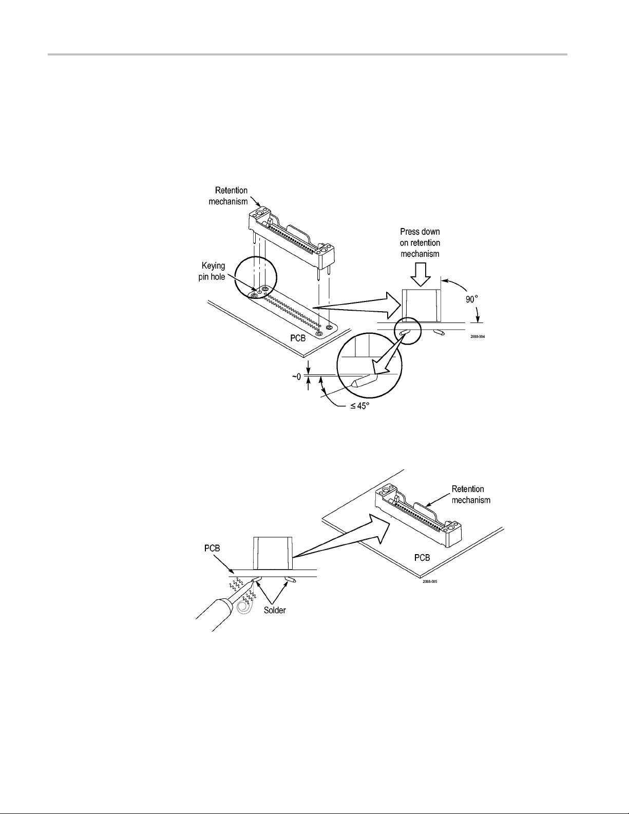
Installing the Midbus Retention Mechanism
Before connecting a midbus probe, you must install the retention mechanism.
The retention m echanism connects the probe head to your circuit board (PCB).
It fits on the footprint and must be soldered to the PCB. To install the retention
mechanism on the circuit board, do the following:
1. Locate the correct footprint. If you intend to use multiple probes, your PCB
has multiple footprints. Be careful to select the correct one.
2. Align the retention mechanism over the footprint so that the keying pin on
the retention mechanism l
(See Figure 5.)
3. Insert the retention mechanism into the holes in the footprint on the PCB.
NOTE. The following two steps are important to ensure that the retention
mechanism is correctly mounted and that the probe makes proper contact with
the PCB.
P6700 Series Serial Analyzer Probes Instruction Manual 5
ines up with the k eying pin hole on the footprint.
Page 22
Operating Basics
4. Hold the retent
the footprint, and the four anchoring posts extend through the circuit board
to the opposite side.
5. Using a pair of needle-nose pliers, grasp one of the posts. Using the circuit
board hole as a fulcrum, bend the post outward so that it secures the
mechanism to the PCB. Bend the other three posts in the same manner.
ion mechanism so that it is firmly flush with the surface of
e 5: Installing the retention mechanism
Figur
6. Solde
Figure 6: Soldering the anchoring posts to the PCB
r the anchoring posts to the PCB.
6 P6700 Series Serial Analyzer Probes Instruction Manual
Page 23

Operating Basics
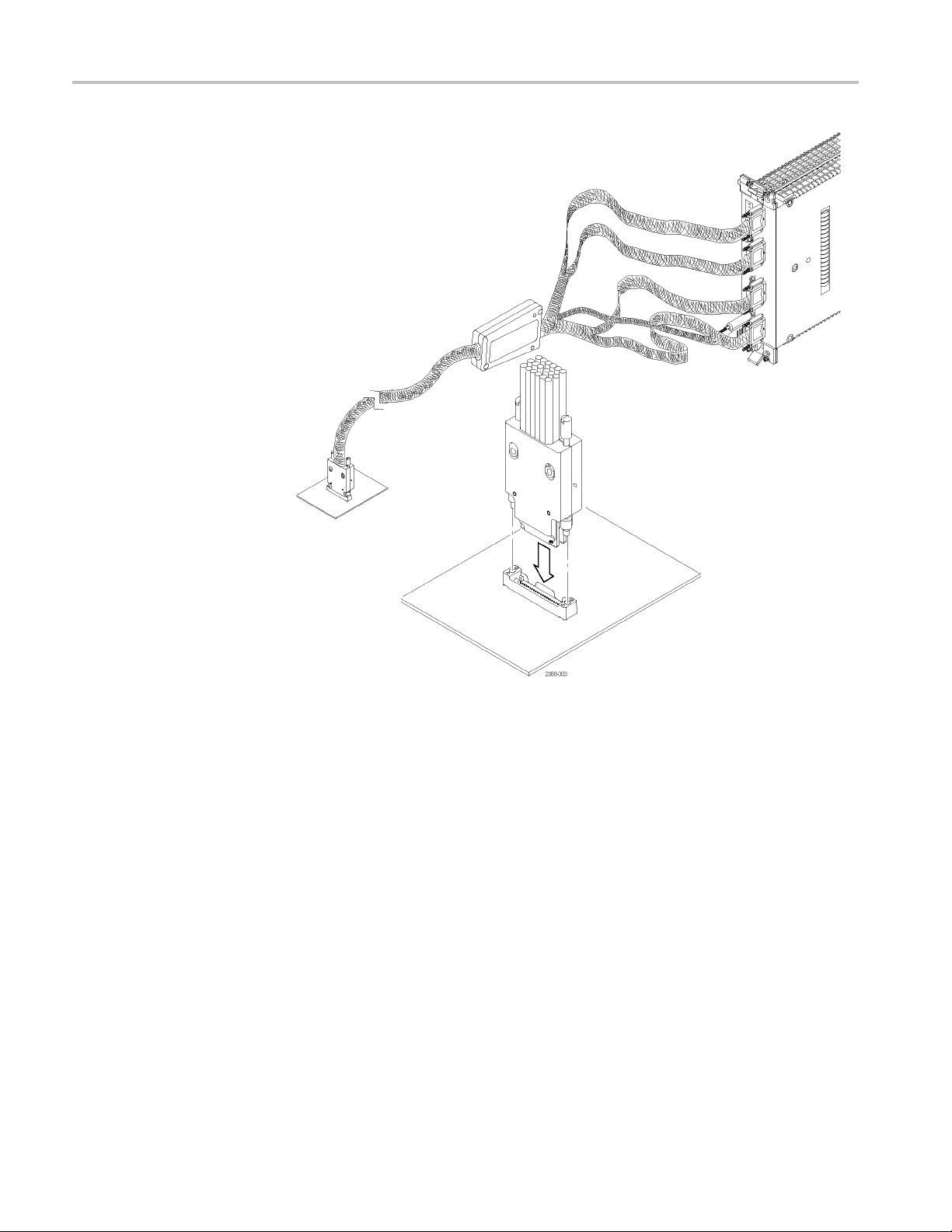
Connecting th
Handling the
Connect the Probe
Probe Head
eMidbusProbe
After you have installed the retention mechanism, you are ready to connect the
midbus probe.
Handle the probe head with care. Keep the following points in mind:
Handle the probe head by the outer plastic casing. Do not touch the contacts
in the center with fingers, tools, wipes, or any other devices.
Do not expose the connector to liquids or dry chemicals.
When connecting the probe, be careful not to touch the probe head contacts to
any other surfaces or components on your circuit board.
Connect
1. Locate the correct retention mechanism. If you intend to use multiple probes,
your PC
one.
2. Align
the probe can only be inserted one way.
the probe by following these steps:
B has multiple retention mechanisms. Be careful to select the correct
the probe head with the retention mechanism. Both are keyed so that
3. Pres
s the probe head into the retention mechanism.
P6700 Series Serial Analyzer Probes Instruction Manual 7
Page 24
Operating Basics
Figure 7: Connecting a probe to the retention mechanism
4. Start both mounting screws in the posts, and tighten them evenly to ensure
that the probe approaches and mates squarely to the PCB. If acc ess is limited,
use the adjustment tool included with your probe. The probe is completely
ened to the PCB when both mounting screws are seated.
fast
5. Refer to the TLA7S08 & TLA7S16 Serial Analyzer Modules Instruction
ual to verify that all channels are acquiring data. If you suspect that
Man
a p oor probe connection may be the source of a problem, refer to the
troubleshooting section of the TLA7S08 & TLA7S16 Serial Analyzer Modules
Instruction Manual.
8 P6700 Series Serial Analyzer Probes Instruction Manual
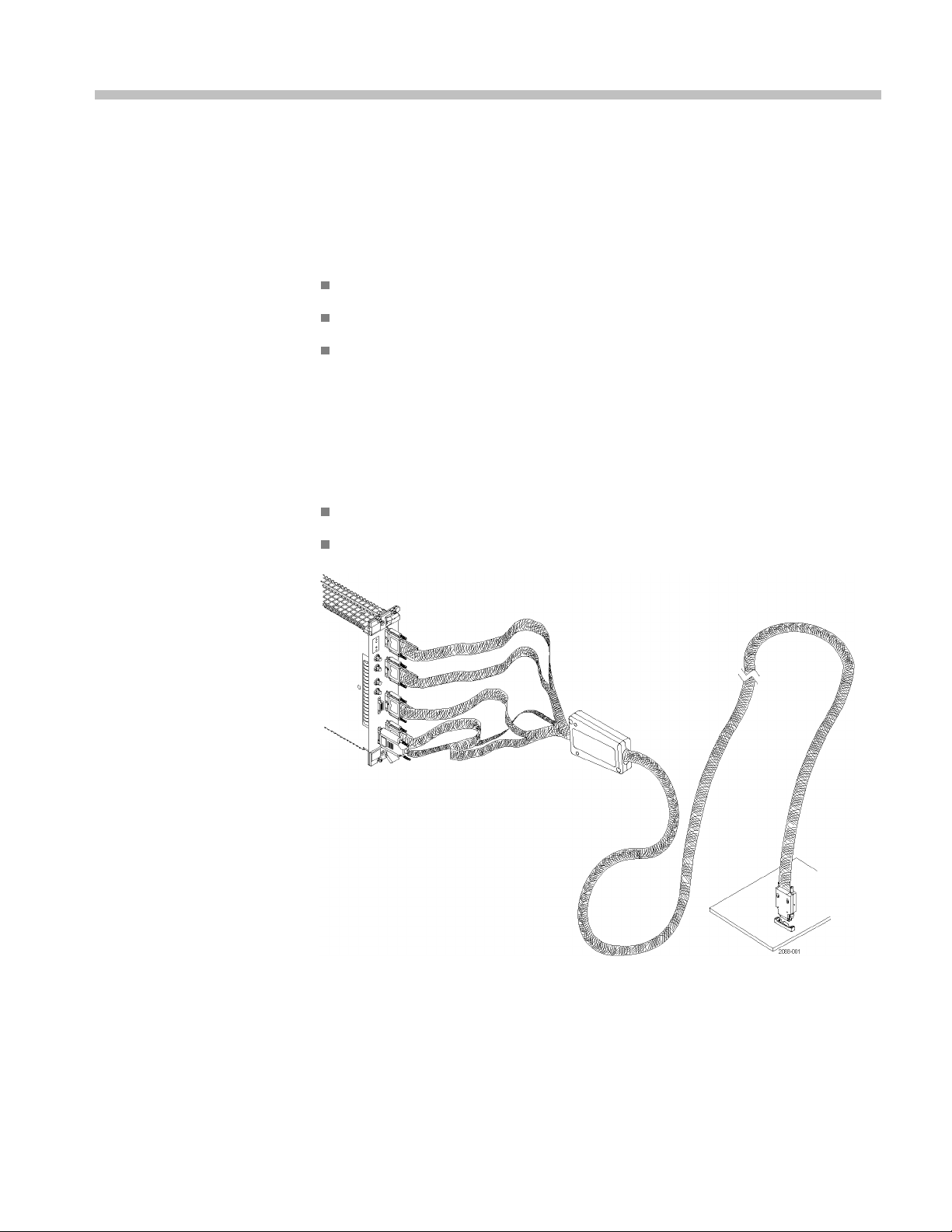
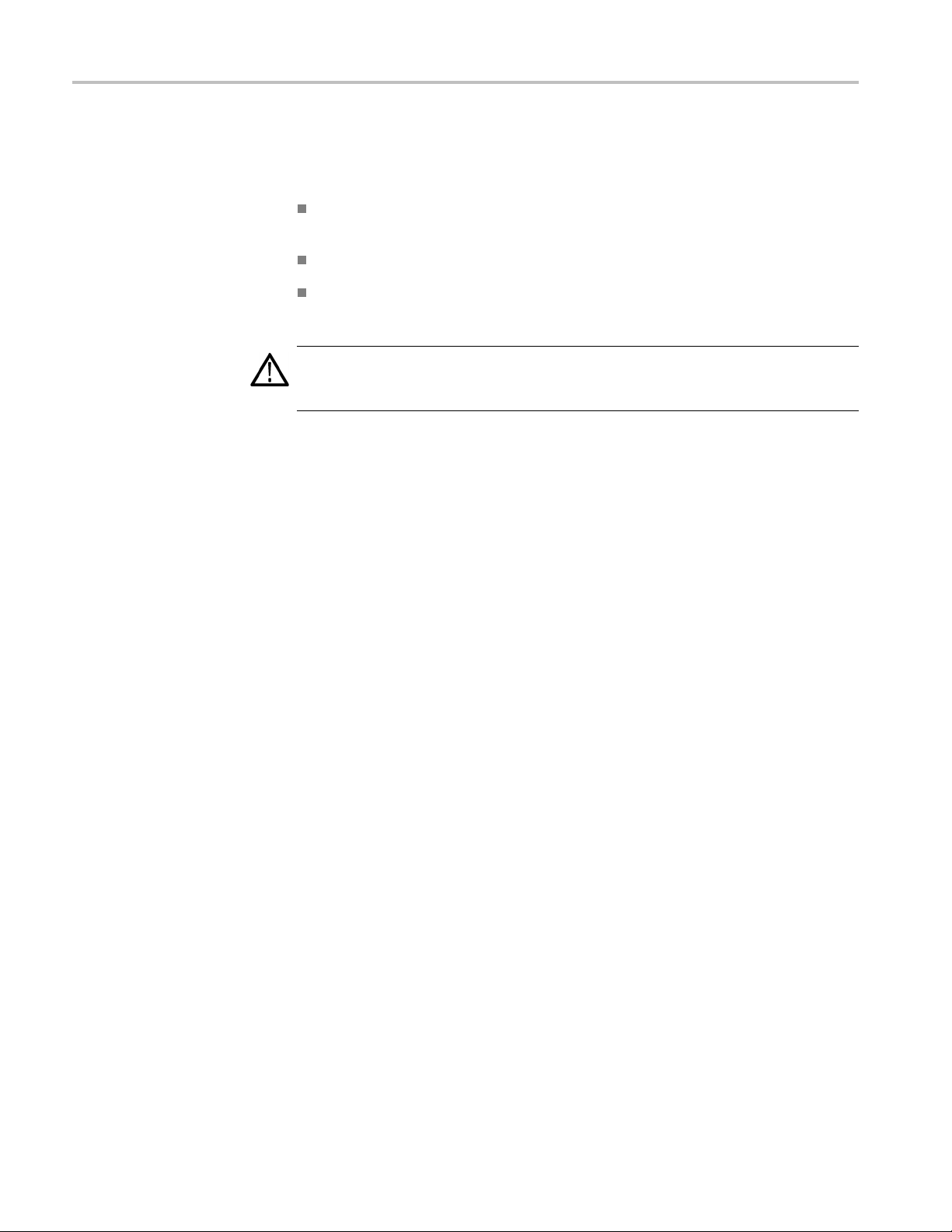
Page 25
Operating Basics
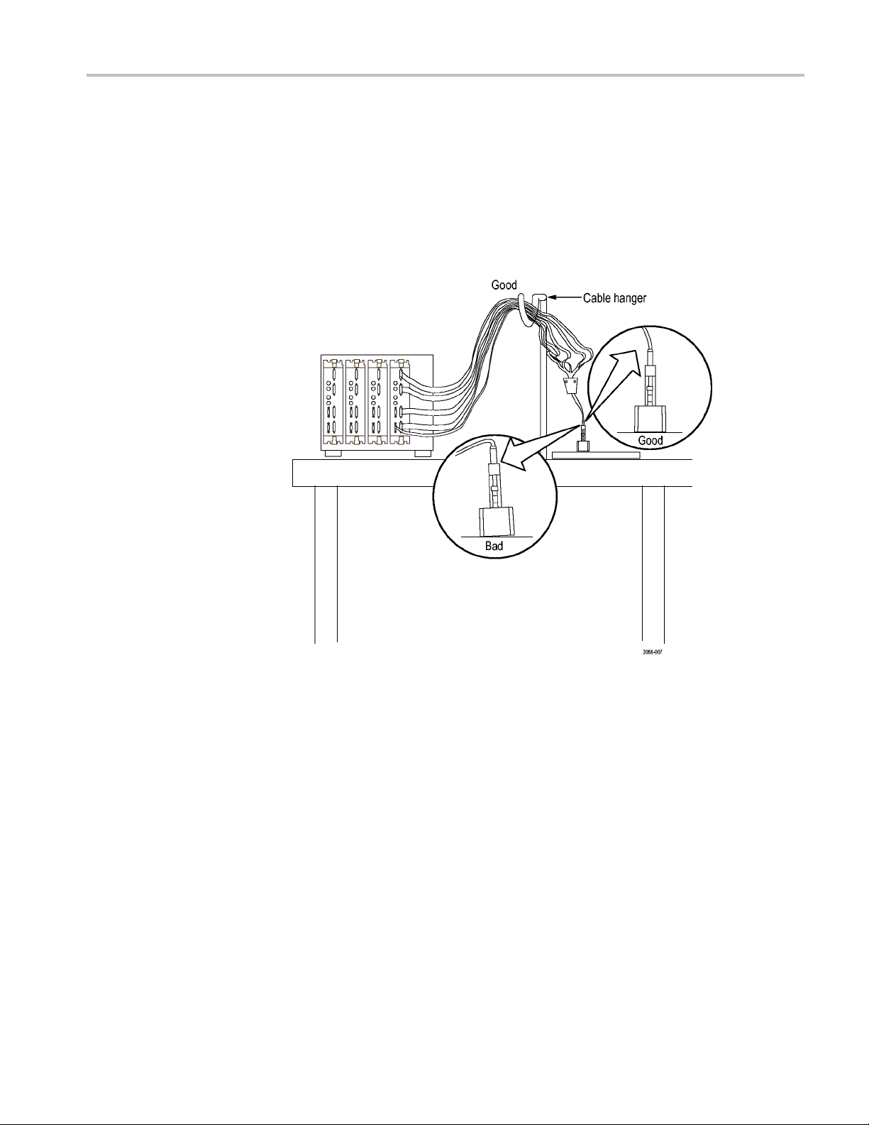
Arranging the
Midbus Probe Cables
Arrange and hang the probe cables so that the probe head is perpendicular to the
circuit board, and tension on the retention mechanism is minimized. Route the
cables as str
degree bend does not occur within three inches of the circuit board surface. (See
Figure 8.) You can route a hanger through the two holes in the cable transition
housing as well.
aight as possible, maximizing the bend radius, and make sure that a 90
Figure 8: Arranging the midbus probe cables
P6700 Series Serial Analyzer Probes Instruction Manual 9
Page 26
Operating Basics
Connecting a S
lot Interposer Probe
Handling the Probe Head
Connect the Probe
Handle the probe head with care. Keep the following points in mind:
Handle the probe head by the outer casing. Do not touch the contacts with
fingers, tools, wipes, or any other devices.
Do not expose the connector to liquids or dry chemicals.
When connecting the probe, be careful not to touch the probe head contacts to
any other surfaces or components on your circuit board.
CAUTION. Static discharge can damage the probe head. Always wear a grounded
antistatic wrist strap whenever handling the probe head. Also verify that anything
to which
Connect the probe by following these steps:
1. Disconnect the power supply to your SUT. Unplug the PC power supply if
2. Locate the correct PCI Express slot.
3. Align the probe with the slot.
the probe head is connected does not carry a static charge.
your SUT is connected to one.
10 P6700 Series Serial Analyzer Probes Instruction Manual
Page 27
Operating Basics
4. Press the probe
head into the slot.
Figure 9: Connecting a slot interposer probe
5. Position the mounting bracket and attach the screws.
6. Press your PCI Express card device into the probe.
NOTE. When the slot interposer is installed, you must connect the power
ector to the module and the module must be powered on whenever the SUT is
conn
powered on.
7. Refer to the TLA7S08 & TLA7S16 Serial Analyzer Modules Instruction
ual to verify that all channels are recognizing signals. If y ou suspect
Man
that a poor probe connection may be the source of a problem, refer to the
troubleshooting section of the TLA7S08 & TLA7S16 Serial Analyzer Modules
Instruction Manual.
P6700 Series Serial Analyzer Probes Instruction Manual 11
Page 28
Operating Basics
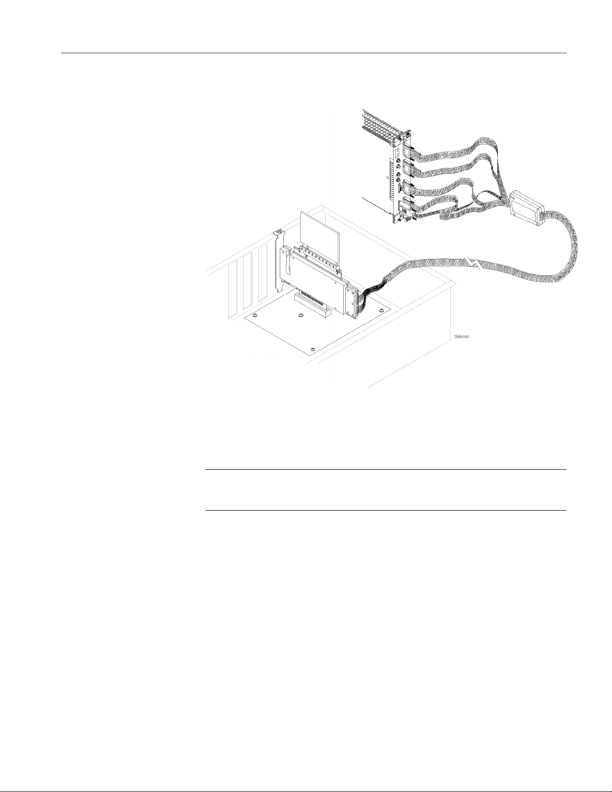
Connecting a Probe to a
Bidirectional X16 Link
To c a p t u r e s i g n
serial analyzer modules to a single slot interposer probe. Connect the probe by
following these steps:
1. Disconnect the power supply to your SUT. If your SUT is connected to a PC
power supply, unplug the power supply..
2. Locate the correct PCI Express slot.
3. Align the pr
4. Press the probe head into the slot.
als from a bidirectional X16 link you need to connect two
obe with the s lot.
5. Pos
6. Press your PCI Express card device into the probe.
7. Connect the probe to the two serial analyzer modules; connect the probe
12 P6700 Series Serial Analyzer Probes Instruction Manual
ition the mounting bracket and attach the screws.
power connector to either serial analyzer module.
Page 29

Operating Basics
NOTE. When the s
connector to either module and the modules must be powered on whenever the
SUT is powered on.
8. Refer to the T
Manual to verify that all channels are recognizing signals. If you suspect
that a poor probe connection may be the source of a problem, refer to the
troubleshooting section of the TLA7S08 & TLA7S16 Serial Analyzer Modules
Instruction Manual.
lot interposer is installed, you must connect the power
LA7S08 & TLA7S16 Serial Analyzer Modules Instruction
P6700 Series Serial Analyzer Probes Instruction Manual 13
Page 30

Operating Basics
Connecting th
Connect to th
Analyzer Module
e Solder-Down Probe
The probe connects to the module and to the probe tip, and the probe tip is
soldered to the circuit. Install the probe by following these steps:
eSerial
1. Plug the signal connector into the module and tighten the hold-down screws.
2. Plug the Power Adapter into the module and tighten the hold-down screws.
3. Plug the power connector into any one of the receptacles on the Power
Adapter.
gure 10: Installing the P6701SD probe
Fi
14 P6700 Series Serial Analyzer Probes Instruction Manual
Page 31

Operating Basics
P75TLRST Solder Tip
Install the pro
NOTE. This tip is very small and must be handled carefully. The following
procedures describe the proper techniques for using the tip.
Connect to the Probe Head. The probe body and tip cable ends a re keyed to
ensure correct installation.
1. Orient the probe body with the + and – inputs on top.
2. Align the tip cable lead with the red band to the + input.
be tip by following these steps:
Figure
3. Grasp
4. To remove the tip, pull the cable tab straight out from the probe body.
CAUTION. Pull only on the cable tab when removing the tip. You can damage the
tip or probe if you pull on the cables.
11: Connecting the P75TLRST tip to the probe head
the cable connector by hand and push the cable into the probe body
until you feel a click. The cable housing is fully seated when it is flush with
the edge of the probe body.
P6700 Series Serial Analyzer Probes Instruction Manual 15
Page 32

Operating Basics
Connect to the C
in this manual for reference. (See Figure 34 on page 34.) You can also design the
tip footprint into your circuit board layout for easier test connections.
To connect the probe tip to your circuit, use the wire and solder that are provided
in the wire replacement kit. The kit includes:
0.004 in (0.1016 mm) wire
0.008 in (0.
SAC305 solder (RoHS compliant)
1. Identify a location where the tip can b e placed, soldered, and secured to your
circuit. You can work with long wires (~1 inch), but keep the finished wire
lengths o
2. Lay the wires against a circuit board pad, trace, or other conductive feature. (If
vias or t
3. Solder the wires to your circuit.
ircuit. The dimensions of the solder tip connections are provided
2032 mm) wire
f the signal and ground connections as short as possible.
hrough-holes are very close, you can thread the wires through them.)
Figure 12: Connecting wires to the circuit
16 P6700 Series Serial Analyzer Probes Instruction Manual
Page 33

Operating Basics
4. Attach tip tape
5. Clean out the tip vias with a solder-wicking material if you are reusing the
tip. Thread th
6. Press the tip to the circuit board and quickly solder the wires to the tip. Keep
all finished
7. Clip off the excess wire from all of the solder joints.
8. Push the end of the tip into the probe head until it seats in the probe head.
to the bottom of the tip.
e wires through the tip.
wire lengths as short as possible.
Figure 13: Connecting the tip to the circuit
9. Secure the probe to the circuit board with tape or with the hook-and-loop
ips and dots that are included with the probe.
str
P6700 Series Serial Analyzer Probes Instruction Manual 17
Page 34

Operating Basics
18 P6700 Series Serial Analyzer Probes Instruction Manual
Page 35

Reference
Probe Dimensions
This section provides guidelines for designing a system to b e tested with a P6700
series probe(s).
The following figure shows dimensions of the P6700 series probes. Both the
P6708 and P
6716 have the same cable lengths.
Figure 14: P6716S dimensions
P6700 Series Serial Analyzer Probes Instruction Manual 19
Page 36

Reference
Figure 15: P6716 cable length dimensions
The following figures show the dimensions of the P6700S slot interposer probes.
re 16: P6716S cable length dimensions
Figu
20 P6700 Series Serial Analyzer Probes Instruction Manual
Page 37

Reference
Figure 17: P6701S, P6704S, and P6708S dimensions
P6700 Series Serial Analyzer Probes Instruction Manual 21
Page 38

Reference
Figure 18: P6701SD dimensions
Figure 19: P75TLRST Solder Tip dimensions
22 P6700 Series Serial Analyzer Probes Instruction Manual
Page 39

Reference
Circuit Board
Mechanical D
Design
esign
Use the following mechanical and electrical guidelines when designing your
system.
This section provides mechanical design details for the midbus probe, including
footprint dimensions, footprint keep-out areas, and trace and via size, and routing
requirements.
Table 2: Re
Paramete
Maximum circuit board
thicknes
Footprint type
Pad finis
commended circuit board design criteria
r
s
h
Descript
3.81 mm (0
PCI Expr
Immersi
level (HASL) also acceptable)
ion
.150 in)
ess Gen1 or Gen2
on gold over nickel (immersion silver and hot air solder
NOTE. Tektronix recommends that the holes made for the retention mechanism
remain unconnected to a ground plane. This prevents overheating the
posts
ground plane and promotes quicker soldering of the retention posts to your PCB.
print dimensions and keep-out area. Design your circuit board layout using
Foot
the following footprint dimensions so that a probe retention mechanism will fit
properly and make good electrical contact with your system. (See Figure 20 on
page 24.) The space around the footprint (keep-out area) represents the area that
will be covered by the retention mechanism.
P6700 Series Serial Analyzer Probes Instruction Manual 23
Page 40

Reference
Figure 20: 8-Channel midbus footprint dimensions and keep-out area
24 P6700 Series Serial Analyzer Probes Instruction Manual
Page 41

Reference
e 21: 16-Channel midbus footprint dimensions and keep-out area
Figur
Routing Considerations for the Midbus Probe Footprint. Routing and simulation
studies have been performed near and through the PCI Express midbus footprint
to determine a best known method for maintaining integrity of the system
nel as well as provide an adequate signal to the serial a nalyzer. However,
chan
the following information does not imply that superior routing techniques do not
exist. It is mandatory that you closely monitor and simulate the routing near and
through the midbus probe to insure that integrity of the system and midbus signal
eye are maximized. Some dimensional details concluded from these simulations
and studies are provided in the following table.
OTE. The via hole size in the following table is a minimum size, based on the
N
assumption that the circuit board is 2.36 mm (0.093-inch) thick.
P6700 Series Serial Analyzer Probes Instruction Manual 25
Page 42

Reference
Table 3: Via and
Parameter Size
Via hole 10 mil
Via annular ring 20 mil
Via antipad 33 mil
Minimum spac
and pad
Trace width 14 mil
Microtrace width 5 mil
Space between traces (before and after
footprint
Space bet
footprint negotiation)
Primary
negotiation)
ween microtraces (before and after
Surface Layer Routing. The following figure shows recommended trace
trace characteristics
e between via annular ring
5mil
14 mil
5mil
routing on the primary surface layer (the surface where the midbus footprint will
be). The solid white pads shown in the diagram are the ground pads.
Figure 22: Recommended trace routing on primary surface layer
Tektronix recommends that you design your footprint so that there are no traces
or vias in the two spaces designated in the following diagram. If your design
requires the use of these two spaces, Tektronix recommends that you fully solder
mask these areas.
26 P6700 Series Serial Analyzer Probes Instruction Manual
Page 43

Figure 23: Via and trace keep-out areas for the P6708 8-Channel probe
Reference
Figure 24: Via and trace keep-out areas for the P6716 16-Channel probe
Inner Layer or Secondary Surface Layer Routing. The following figures show
suggested trace routing on the inner layer, and the secondary surface layer (the
surface opposite from where the midbus footprint will be). The solid white pads
shown in the diagram a re the ground pads.
Figure 25: Recommended trace routing on inner or secondary surface layer (primary
layer pads shown)
P6700 Series Serial Analyzer Probes Instruction Manual 27
Page 44

Reference
Figure 26: Recommended trace routing on inner or secondary surface layer (primary
layer pads not shown)
Clock Cable Three-Pin
Connector
If you intend to use a midbus probe and a clock cable, a three-pin micro-terminal
strip connector must be installed on your SUT. A non-intrusive clock cable
(Tektro
nix part number, 672-6285-00) has two SMA connectors on one end
(+ and –), and a small circuit board with a mating three-pin connector on the other.
Only one connector is needed, even if more than one TLA7S08 or TLA7S16
module is used. In this case, a “jumper” clock cable with SMA connectors on
each end (+ and –) can connect the two modules and share the clock signal.
Tektronix suggests installing the following three-pin connector (or similar):
Through hole: Samtec® TMS 103-02-S-S
(1x3,0.05centerspacing)
face mount: Samtec® FTR 103-02-S-S
Sur
(1x3,0.05centerspacing)
ble 4: Clock cable three-pin connector pin assignments
Ta
Signal Pin number
REFCLKp 1 (or 3)
GND
REFCLKn 3 (or 1)
1
The serial analyzer module is not sensitive to the polarity of the reference clock signal. The clock cable connector
can be attached in either orientation.
1
2
1
28 P6700 Series Serial Analyzer Probes Instruction Manual
Page 45

Reference
Figure 27: Clock cable connector dimensions
For more specific information on keep-out volumes for particular system
configurations, contact your local Tektronix representative.
P6700 Series Serial Analyzer Probes Instruction Manual 29
Page 46

Reference
P6701SD Probe Solder Tip
(P75TLRST)
The P75TLRST pr
is composed of a small form factor interconnect circuit board with SMD0402
damping resistors and a set of vias for wire attachment to the SUT. The circuit
board vias are designed for both 4 mil and 8 mil wire and a special high tensile
strength wire is supplied as part of the wire accessory kit. The expanded v iew of
the probe tip shows the location of the + and – signal inputs as well as the two
ground refe
Figure 2
Attach
a polarized G3PO dual connector block. The 3GPO connectors use a miniature,
high frequency design that enables quick and easy installation of the P75TLRST
solder tip. The G3PO connector block of the probe tip is inserted into the input
nose piece on the end of the P6701SD Serial Analyzer probe body. The probe
body contains a mating, polarized G3PO connector block with attached G3PO
ector bullets.
conn
rence connections. (See Figure 28.)
8: P75TLRST TriMode Long Reach Solder Tip
ed to the circuit board a re a pair of very low skew (<1ps) coaxial cables and
obe tip is designed for solder-down probing applications. It
The connector bullets are a part of the G3PO connector design, providing a
f-aligning interconnect mechanism between G3PO connectors. The G3PO
sel
connector in the probe body is designed to have higher detent force than the probe
tip connectors, which is intended to ensure that the G3PO bullets remain in the
probe body connector when disconnected.
The probe body nose piece, with its integral spring mechanism, helps to provide a
self-aligning mechanism for hand insertion of the probe tip. The probe body nose
springs also give a secure capture of the probe tip connector after insertion.
Release of the probe tip is assisted by using the wire-connected cable release
holder on the probe tip connector. This probe tip release holder should always be
used rather than pulling on the probe tip cables, which may cause tip cable damage.
The recommended wire attachment method is to first solder the wires to the SUT,
being careful to minimize the wire length of the signal and ground connections.
This is followed by threading the wires through the probe tip board vias, being
careful to achieve as symmetrical a wire pattern as possible between the two
signal inputs and a very short ground connection.
30 P6700 Series Serial Analyzer Probes Instruction Manual
Page 47

Reference
Finally, the at
circuit board. Any excess wire lead length extending through the probe tip board
should be removed to minimize possible signal reflection problems. Because of
the limited mechanical strength of the wire interconnect and probe tip circuit
board, the solder-down probe tip should be taped down at the SUT for strain
relief. Although the accessory kit includes adhesive strips that can be used for the
strain reli
attachment if room is available at the SUT.
The lead le
must be kept as short as possible to preserve the integrity of the measured signal.
Typical wire lengths range from 0.010 in. to 0.100 in. (See Figure 29.)
tachment is completed by soldering the wires on top of the probe tip
ef of the probe tip, the use of mylar tape will generally provide stronger
ngth of the connection wires between the probe tip board and the SUT
ure 29: Typical wire length from probe tip to circuit
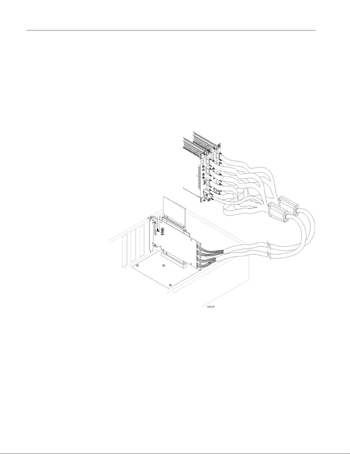
Fig
following four figures illustrate the signal integrity effect on the P75TLRST
The
solder tip when used with different lengths of tip wire. Signal fidelity is best when
the wire length is kept as short as possible. The step generator that was used as
a signal source for these screenshots has a 30 ps 10-90% rise time. The table in
each figure contains data for two rise time m easurements (10-90% and 20-80%).
These screenshots can be used as a guide to gauge the effects of wire length, but
actual results may vary depending on the other factors like characteristics of the
device under test (for example, rise time and impedance), and the precision of
the solder connection.
P6700 Series Serial Analyzer Probes Instruction Manual 31
Page 48

Reference
Figure 30: P75TLRST solder tip with 0.010 inch of tip wire
Figure 31: P75TLRST solder tip with 0.050 inch of tip wire
32 P6700 Series Serial Analyzer Probes Instruction Manual
Page 49
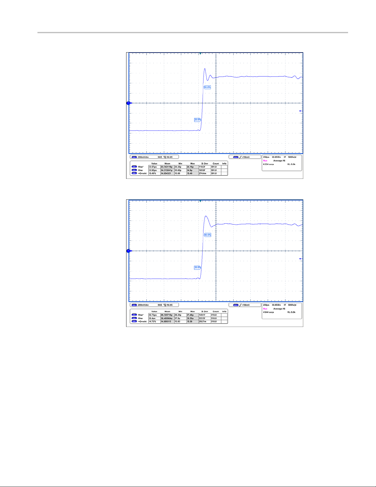
Figure 32: P75TLRST solder tip with 0.100 inch of tip wire
Reference
Figure 33: P75TLRST solder tip with 0.200 inch of tip wire
P6700 Series Serial Analyzer Probes Instruction Manual 33
Page 50

Reference
The following fi
Figure 34: P75TLRST TriMode Long Reach Solder Tip dimensions
Electric
al Design
For the serial analyzer module to reliably capture logical transactions on the bus,
adequate signal eye must be available at the point of probing while the probe is
connected. This can be verified by electrical simulation using the load model of
the P67
00 Series probe.
gure shows the dimensions of the P75TLRST Solder Tip.
Eye requirements are defined at the point of probing (midbus footprint, solder tip
for the solder-down probe, or the slot connector for the slot interposer probe)
input
and are measured by eye height and eye width, forming a diamond shape.
Figure 35: Signal eye measurements (time versus voltage)
The following specifications limit the electrical distance between the driver
pin and the point of probing. When analyzing both directions of an electrically
ong PCI Express link, you might need to design your system with two separate
l
footprints to maintain adequate signal eye. Eye requirements apply regardless of
circuit board material and infrastructure.
34 P6700 Series Serial Analyzer Probes Instruction Manual
Page 51

Reference
Table 5: Probe E
ye Requirements
Parameter Description
Midbus probe
Minimum eye height
1
at footprint p
ad
Minimum eye width
at footprint
pad
30 mV (single-
0.53 UI if jit
≤ 40 MHz are not present
If jitter frequency components of ≤ 40 MHz are
present, th
in the graph to the jitter of the signal. (See
Figure 36 on page 36.)
probe
Minimum eye height
at solder tip input
Minimum eye width
at solder tip input
30 mV (single-ended)Solder-down
1
0.53 UI if jitter frequency components of
≤ 40 MHz are
If jitter frequency components of ≤ 40 MHz are
present, then apply the filter function described
in the gra
ph to the jitter of the signal. (See
Figure 36 on page 36.)
probe
Minimum
at probe connection
point
Minimum eye width
at probe connection
point
1
eye height
60 mV (single-ended)Slot interposer
0.58 UI if jitter frequency components of
≤ 40 MHz
If jitter frequency components of ≤ 40 MHz are
present, then apply the filter function described
raph to the jitter of the signal. (See
in the g
Figure 36 on page 36.)
Unit Interval Gen1
Unit Interval Gen2
1
Eye Height/Width values apply to both data rates.
2
irements valid for 10
Requ
information, contact your local Tektronix representative.
–12
BER. Refer to the following graphs for probe input jitter tolerances. For further
400 ps
200 p
s
1
ended)
ter frequency components of
2
en apply the filter function described
not present
are not present
2
2
P6700 Series Serial Analyzer Probes Instruction Manual 35
Page 52

Reference
Figure 36: Periodic jitter gain function
Measuring signal eye. Tektronix recommends using a Tektronix DPO70000 series
or DSA70000 series oscilloscope with a P7500 series probe with solder-down tips
for most accurate results. If your system does not allow you to use solder-down
tips, use the handheld Precision Differential Probing Module (Tektronix part
r P75PDPM). Tektronix recommends using TDSJIT3 Advanced software
numbe
to take signal eye measurements. Tektronix RT-Eye software is also acceptable.
For instructions on using TDSJIT3 Advanced and RT Eye software, go t o
Tektronix.com/manuals, or contact your local Tektronix representative.
P6700 Series midbus probe circuit impact. Tektronix has provided two
chstone® models (sdd12wop.dat and sdd12wp.dat). (See page 73, Reference
Tou
Files.) These models simulate the impact of the P6700 Series midbus probe (8
or 16 channel) retention mechanisms with and without the probe installed. This
is actual S-parameter measured data using real probes and retentions. Graphical
representation of the data is provided in the next two graphs.
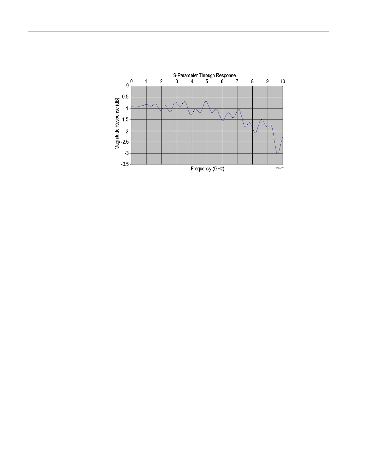
The first graph shows the frequency response of a transmission line loaded with a
P6700 midbus probe retention. (See Figure 37 on page 37.)
36 P6700 Series Serial Analyzer Probes Instruction Manual
Page 53

Reference
Figure 37: S-parameter data of retention mechanism only
The second graph shows the frequency response of a transmission line loaded
with a P6700 midbus probe retention and a probe. (See Figure 39.)
Figure 38: S-parameter data of retention mechanism plus P6700 Series midbus probe
P6700S Series Slot Interposer Probe circuit impact. Tektronix has provided
Touchstone® models to simulate the impact of a P6700S Series slot interposer
probe. (See page 73, Reference Files.) This is actual S-parameter measured data
using a real P6700S interposer probe.
P6701SD Solder-Down Probe circuit impact. Tektronix has provided a
Touchstone® model (P6701SD.dat) to simulate the impact o f a P6701SD
solder-down probe and P75TLRST solder tip. (See page 73, Reference Files.)
This is actual S-parameter measured data using a real P6701SD solder-down
probe. Graphical representation of the data is provided in the following graph.
P6700 Series Serial Analyzer Probes Instruction Manual 37
Page 54
Reference
Reference Clock Signal
It shows the fre
solder-down probe and P75TLRST solder tip.
Figure 39
The TLA7S08 & TLA7S16 Serial Analyzer modules can recognize a clock
signal f
embedded in the data.
rom a cable connection to the SUT, or by recovering the clock signal
quency response of a transmission line loaded with a P6701SD
: S-parameter data of P6701SD Solder-Down probe
Recognize the clock signal embedded in the data stream. A stable reference
signal is generated by the serial analyzer and synchronized with the embedded
clock signal. A clock cable connection is not required, since the logic analyzer
gnizes the embedded signal from the probe.
reco
The transfer rate of the serial link must be 2.5 GT/s ± 300 ppm (PCI Express
) or 5.0 GT/s ± 300 ppm (PCI Express Gen 2). If the transfer rate is not
Gen 1
within this range, the module will not capture the data reliably.
SC (spread spectrum clocking) is enabled, and your PCI Express link uses
If S
power management states, you must connect a clock cable to the SUT and set the
reference clock source to SUT so that the module will capture data reliably.
Recognize the clock signal by directly connecting to the SUT with a clock
cable. Tektronix recommends connecting a clock cable to ensure that data is
ccurately synchronized with the clock signal.
a
If you intend to use a midbus probe, you must install a three-pin connector on
your SUT to connect to the clock cable. (See page 28, Clock Cable Three-Pin
Connector.) Slot interposer probes already have this connector installed on the
probe.
38 P6700 Series Serial Analyzer Probes Instruction Manual
Page 55

Reference
Figure 4
0: Slot Interposer probe with a clock cable connected
Table 6: Reference clock electrical requirements
module requirement
Serial
Differential Voltage at Ref Clock Attach Point Vdiff
Absolute Voltage Limit at Ref Clock Attach Point
rence Clock Frequency –100 MHz
Refe
Reference Clock Frequency –100 MHz + 10%
Reference Clock Frequency –100 MHz - 10%
ference Clock Frequency –125 MHz
Re
1
Reference Clock Total Jitter RefClkJitter
1
With SSC (spread spectrum clocking) enabled or disabled
2
Vdiff= |2*(Vrefclockp - Vrefclockn)|
Symbol Minimu
2
Vabs 0 V
Freq100
1
Freq100 +10% - 110 MHz +/-300 ppm -
1
Freq100 -10% - 90 MHz +/-300 ppm -
Freq125
m
0.8 V
- 100 M
-12
-
-
l
Typica
-
-
Hz +/-300 ppm
5 MHz +/-300 ppm
<1 MHz: 25 ps p-p
>1 MHz: 200 ps p-p
Maximu
2.0 V
3.3 V
m
-
-
-
-
P6700 Series Serial Analyzer Probes Instruction Manual 39
Page 56

Reference
Midbus Footpr
int Pin and Probe Channel Assignments
The following figure shows the standard pin assignments for a PCI Express
8-channel footprint.
Figure 41: P6708 8-Channel probe footprint pin assignments
The following figure shows the standard pin assignments for a PCI Express
16-channel footprint.
General Guidelines for
Pin-Channel Assignment
Figure 42: P6716 16-Channel probe footprint pin assignments
Tektronix strongly recommends that you design your system so that pins are
assigned to channels according to the following guidelines and the standard
formats listed in the tables. The formats listed in the tables were created so
that each module-end probe connector contains the wires c onnected to adjacent
differential pairs on the footprint.
Figure 43: 8-Channel midbus footprint connection module connector
40 P6700 Series Serial Analyzer Probes Instruction Manual
Page 57

Figure 44: 16-Channel midbus footprint connection module connector
Reference
The serial analyzer software is designed to be easily configured based on these
standard formats. If your system design does not allow you to follow these
guideli
rewire the connector at the module end of the probe. (See page 57, Rearranging
Wires in the Probe Connector.)
nes, or if a footprint is incorrectly wired, you may have to disassemble and
The differential pairs that make up a PCI Express link must be connected to
specific pads (pins) on the footprint
The polarity of the differential pairs can be swapped, if required, for routing
ream and downstream channels can be swapped on a footprint, if
Upst
required, for routing
ire links can be reversed compared to the suggested routing
Ent
P6700 Series Serial Analyzer Probes Instruction Manual 41
Page 58

Reference
Key concepts fo
Each channel is connected to either an upstream or downstream differential
pair.
Signal name = C[number][p (positive) or n (negative)]
Example: C3p = the positive signal of the differential pair connected to
channel three
Channels are grouped together in sets of four in probe-to-module connectors.
All channels in the probe-to-module connector must come from the same
direction.
To ensure that all lanes from one direction of the link are connected to the top
two connectors on a TLA7S16 or to the top connector of a TLA7S08, refer
to the connector illustrations. (See Figure 43 on page 40.) (See Figure 44
on page 41.) Ensure that all lanes going to the bottom two connectors of
the TLA
direction.
llowing tables show footprint p in-channel assignments for PCI Express
The fo
links of various standard recommended configurations.
r the channel mapping tables.
7S16 (or the bottom connector of the TLA7S08) are from the same
42 P6700 Series Serial Analyzer Probes Instruction Manual
Page 59

Reference
16-Channel PC
I Ex press
Midbus Pin Assignments
Table 7: X16 uni
Pin # Signal name Pin # Signal name
2
4
6
8
10
12
14
16
18
20
22
24
26
28
30
32
34
6
3
8
3
40
42
44
46
48
G2 GND
directional link
GND
C1p
C1n
GND
C3p
C3n
GND
C5p
C5n
GND
C7p
C7n
GND
C9p
C9n
GND
C11p
C11n
GND
C13p
C13n
GND
C15p
C15n
G1 GND
1
3
5
7
9
11
13
15
17
19
21
23
25
27
29
31
33
3
3
39
41
43
45
47
5
7
C0p
C0n
GND
C2p
C2n
GND
C4p
C4n
GND
C6p
C6n
GND
C8p
C8n
GND
C10p
C10n
GND
C12p
C12n
GND
C14p
C14n
GND
P6700 Series Serial Analyzer Probes Instruction Manual 43
Page 60

Reference
Table 8: X8 bidi
Pin # Signal name Pin # Signal name
2
4
6
8
10
12
14
16
18
20
22
24
26
28
30
32
34
6
3
8
3
40
42
44
46
48
G2 GND
rectional link
GND
C0p- Downstream
C0n- Downstream
GND
C1p- Downstream
C1n- Downstream
GND
C2p- Downstream
C2n- Downstream
GND
C3p- Downstream
C3n- Downstream
GND
C4p- Downstream
C4n- Downstream
GND
C5p- Downstream
C5n- Downstream
GND
C6p- Downstream
C6n- Downstream
GND
C7p- Downstream
C7n- Downstream
G1 GND
1
3
5
7
9
11
13
15
17
19
21
23
25
27
29
31
33
3
3
39
41
43
45
47
5
7
C0p- Upstream
C0n- Upstream
GND
C1p- Upstream
C1n- Upstream
GND
C2p- Upstream
C2n- Upstream
GND
C3p- Upstream
C3n- Upstream
GND
C4p- Upstream
C4n- Upstream
GND
C5p- Upstream
C5n- Upstream
GND
C6p- Upstream
C6n- Upstream
GND
C7p- Upstream
C7n- Upstream
GND
44 P6700 Series Serial Analyzer Probes Instruction Manual
Page 61

Reference
Table 9 : X8 (2) u
Pin # Signal name Pin # Signal name
2
4
6
8
10
12
14
16
18
20
22
24
26
28
30
32
34
6
3
8
3
40
42
44
46
48
G2 GND
nidirectional links
GND
C1p- DirectionA
C1n- DirectionA
GND
C3p- DirectionA
C3n- DirectionA
GND
C5p- DirectionA
C5n- DirectionA
GND
C7p- DirectionA
C7n- DirectionA
GND
C1p- DirectionB
C1n- DirectionB
GND
C3p- DirectionB
C3n- DirectionB
GND
C5p- DirectionB
C5n- DirectionB
GND
C7p- DirectionB
C7n- DirectionB
G1 GND
1
3
5
7
9
11
13
15
17
19
21
23
25
27
29
31
33
3
3
39
41
43
45
47
5
7
C0p- DirectionA
C0n- DirectionA
GND
C2p- DirectionA
C2n- DirectionA
GND
C4p- DirectionA
C4n- DirectionA
GND
C6p- DirectionA
C6n- DirectionA
GND
C0p- DirectionB
C0n- DirectionB
GND
C2p- DirectionB
C2n- DirectionB
GND
C4p- DirectionB
C4n- DirectionB
GND
C6p- DirectionB
C6n- DirectionB
GND
P6700 Series Serial Analyzer Probes Instruction Manual 45
Page 62

Reference
Table 10: X4 bid
Pin # Signal name Pin # Signal name
2
4
6
8
10
12
14
16
18
20
22
24
26
28
30
32
34
6
3
8
3
40
42
44
46
48
G2 GND
irectional link
GND
C0p- Downstream1
C0n- Downstream1
GND
C1p- Downstream1
C1n- Downstream1
GND
C2p- Downstream1
C2n- Downstream1
GND
C3p- Downstream1
C3n- Downstream1
GND
C0p- Downstream2
C0n- Downstream2
GND
C1p- Downstream2
C1n- Downstream2
GND
C2p- Downstream2
C2n- Downstream2
GND
C3p- Downstream2
C3n- Downstream2
G1 GND
1
3
5
7
9
11
13
15
17
19
21
23
25
27
29
31
33
3
3
39
41
43
45
47
5
7
C0p- Upstream1
C0n- Upstream1
GND
C1p- Upstream1
C1n- Upstream1
GND
C2p- Upstream1
C2n- Upstream1
GND
C3p- Upstream1
C3n- Upstream1
GND
C0p- Upstream2
C0n- Upstream2
GND
C1p- Upstream2
C1n- Upstream2
GND
C2p- Upstream2
C2n- Upstream2
GND
C3p- Upstream2
C3n- Upstream2
GND
46 P6700 Series Serial Analyzer Probes Instruction Manual
Page 63

Reference
Table 11: X 4 (2)
Pin # Signal name Pin # Signal name
2
4
6
8
10
12
14
16 Not conn
18 Not connected 17
20
22 Not connected 21 Not connected
24 Not connected 23
26
28
30
32
34
36
38
40 Not connected 39 Not connected
42 Not connected 41
44
46 Not connected 45 Not connected
48 Not connected 47
G2 GND
unidirectional links
GND
C1p- DirectionA
C1n- DirectionA
GND
C3p- DirectionA
C3n- DirectionA
GND
ected
GND
GND
C1p- DirectionB
C1n- DirectionB
GND
C3p- DirectionB
C3n- DirectionB
GND
GND
G1 GND
1
3
5
7
9
11
13 Not conn
15 Not conn
19 Not connected
25
27
29
31
33
35
37 Not connected
43 Not connected
C0p- DirectionA
C0n- DirectionA
GND
C2p- DirectionA
C2n- DirectionA
GND
ected
ected
GND
GND
C0p- DirectionB
C0n- DirectionB
GND
C2p- DirectionB
C2n- DirectionB
GND
GND
GND
P6700 Series Serial Analyzer Probes Instruction Manual 47
Page 64

Reference
Table 12: X2 bid
Pin # Signal name Pin # Signal name
2
4
6
8
10
12
14
16 Not conn
18 Not connected 17
20
22 Not connected 21 Not connected
24 Not connected 23
26
28
30
32
34
36
38
40 Not connected 39 Not connected
42 Not connected 41
44
46 Not connected 45 Not connected
48 Not connected 47
G2 GND
irectional link
GND
C0p- Downstream1
C0n- Downstream1
GND
C1p- Downstream1
C1n- Downstream1
GND
ected
GND
GND
C0p- Downstream2
C0n- Downstream2
GND
C1p- Downstream2
C1n- Downstream2
GND
GND
G1 GND
1
3
5
7
9
11
13 Not conn
15 Not conn
19 Not connected
25
27
29
31
33
35
37 Not connected
43 Not connected
C0p- Upstream1
C0n- Upstream1
GND
C1p- Upstream1
C1n- Upstream1
GND
ected
ected
GND
GND
C0p- Upstream2
C0n- Upstream2
GND
C1p- Upstream2
C1n- Upstream2
GND
GND
GND
48 P6700 Series Serial Analyzer Probes Instruction Manual
Page 65

Reference
Table 13: X2 (2)
Pin # Signal name Pin # Signal name
2
4
6
8
10 Not connec
12 Not connected 11
14
16 Not connected 15 Not connected
18 Not connected 17
20
22 Not connected 21 Not connected
24 Not co
26
28
30
32
34 No
36 Not connected 35
38
40 Not connected 39 Not connected
42 Not connected 41
44
46 Not connected 45 Not connected
48 Not connected 47
G2 GND
unidirectional links
GND
C1p- DirectionA
C1n- DirectionA
GND
ted
GND
GND
nnected
GND
C1p- DirectionB
C1n- DirectionB
GND
t connected
ND
G
GND
G1 GND
1
3
5
7
9 Not connec
13 Not connected
19 Not connected
23
25
27
29
31 Not
33 No
37 Not connected
43 Not connected
C0p- DirectionA
C0n- DirectionA
GND
Not connec
GND
GND
GND
C0p- DirectionB
C0n- DirectionB
GND
t connected
GN
GND
GND
ted
ted
connected
D
P6700 Series Serial Analyzer Probes Instruction Manual 49
Page 66

Reference
Table 14: X1 bid
Pin # Signal name Pin # Signal name
2
4
6
8
10 Not connec
12 Not connected 11
14
16 Not connected 15 Not connected
18 Not connected 17
20
22 Not connected 21 Not connected
24 Not co
26
28
30
32
34 No
36 Not connected 35
38
40 Not connected 39 Not connected
42 Not connected 41
44
46 Not connected 45 Not connected
48 Not connected 47
G2 GND
irectional link
GND
C0p- Downstream1
C0n- Downstream1
GND
ted
GND
GND
nnected
GND
C0p- Downstream2
C0n- Downstream2
GND
t connected
ND
G
GND
G1 GND
1
3
5
7
9 Not connec
13 Not connected
19 Not connected
23
25
27
29
31 Not
33 No
37 Not connected
43 Not connected
C0p- Upstream1
C0n- Upstream1
GND
Not connec
GND
GND
GND
C0p- Upstream2
C0n- Upstream2
GND
t connected
GN
GND
GND
ted
ted
connected
D
50 P6700 Series Serial Analyzer Probes Instruction Manual
Page 67

Reference
Table 15: X1 (2)
Pin # Signal name Pin # Signal name
2
4 Not connect
6 Not connect
8
10 Not connec
12 Not connected 11
14
16 Not connected 15 Not connected
18 Not connected 17
20
22 Not connected 21 Not connected
24 Not co
26
28 Not c
30 Not
32
34 No
36 Not connected 35
38
40 Not connected 39 Not connected
42 Not connected 41
44
46 Not connected 45 Not connected
48 Not connected 47
G2 GND
unidirectional links
GND
ed
ed
GND
ted
GND
GND
nnected
GND
onnected
connected
GND
t connected
ND
G
GND
G1 GND
1
3
5
7
9 Not connec
13 Not connected
19 Not connected
23
25
27
29
31 Not
33 No
37 Not connected
43 Not connected
C0p- DirectionA
C0n- DirectionA
GND
Not connec
GND
GND
GND
C0p- DirectionB
C0n- DirectionB
GND
t connected
GN
GND
GND
ted
ted
connected
D
P6700 Series Serial Analyzer Probes Instruction Manual 51
Page 68

Reference
8-Channel PCI
Express
Midbus Pin Assignments
Table 16: X8 uni
Pin # Signal name Pin # Signal name
2
4
6
8
10
12
14
16
18
20
22
24
directional link
GND
C1p- DirectionA
C1n- DirectionA
GND
C3p- DirectionA
C3n- DirectionA
GND
C5p- DirectionA
C5n- DirectionA
GND
C7p- DirectionA
C7n- DirectionA
1
3
5
7
9
11
13
15
17
19
21
23
C0p- DirectionA
C0n- DirectionA
GND
C2p- DirectionA
C2n- DirectionA
GND
C4p- DirectionA
C4n- DirectionA
GND
C6p- DirectionA
C6n- DirectionA
GND
Table 17: X4 bidirectional link
Pin # Signal name Pin # Signal name
2
4
6
8
1
1
14
16
18
20
22
24
GND
C1p- Upstream
C1n- Upstream
GND
0
2
C3p- Upstream
C3n- Upstream
GND
C1p- Downstream
C1n- Downstream
GND
C3p- Downstream
C3n- Downstream
1
3
5
7
9
1
13
15
17
19
21
23
C0p- Upstream
C0n- Upstream
GND
C2p- Upstream
C2n- Upstream
1
GND
C0p- Downstream
C0n- Downstream
GND
C2p- Downstream
C2n- Downstream
GND
52 P6700 Series Serial Analyzer Probes Instruction Manual
Page 69

Reference
Table 18: X4 (2)
Pin # Signal name Pin # Signal name
2
4
6
8
10
12
14
16
18
20
22
24
unidirectional links
GND
C1p- DirectionA
C1n- DirectionA
GND
C3p- DirectionA
C3n- DirectionA
GND
C1p- DirectionB
C1n- DirectionB
GND
C3p- DirectionB
C3n- DirectionB
1
3
5
7
9
11
13
15
17
19
21
23
C0p- DirectionA
C0n- DirectionA
GND
C2p- DirectionA
C2n- DirectionA
GND
C0p- DirectionB
C0n- DirectionB
GND
C2p- DirectionB
C2n- DirectionB
GND
Table 19: X4 unidirectional link and a X2 unidirectional link
Pin # Signal name Pin # Signal name
2
4
6
8
10
12
14
16
18
20
22 Not connected 21 Not connected
24 Not connected 23
GND
C1p- DirectionA
C1n- DirectionA
GND
C3p- DirectionA
C3n- DirectionA
GND
C1p- DirectionB
C1n- DirectionB
GND
1
3
5
7
9
11
13
15
17
19 Not connected
C0p- DirectionA
C0n- DirectionA
GND
C2p- DirectionA
C2n- DirectionA
GND
C0p- DirectionB
C0n- DirectionB
GND
GND
P6700 Series Serial Analyzer Probes Instruction Manual 53
Page 70

Reference
Table 20: X4 uni
Pin # Signal name Pin # Signal name
2
4
6
8
10
12
14
16 Not conn
18 Not conn
20
22 Not con
24 Not connected 23
directional link and a X1 unidirectional link
GND
C1p- DirectionA
C1n- DirectionA
GND
C3p- DirectionA
C3n- DirectionA
GND
ected
ected
GND
nected
1
3
5
7
9
11
13
15
17
19 Not con
21 Not con
C0p- DirectionA
C0n- DirectionA
GND
C2p- DirectionA
C2n- DirectionA
GND
C0p- DirectionB
C0n- DirectionB
GND
nected
nected
GND
Table 21: X2 bidirectional link
Pin # Signal name Pin # Signal name
2
4
6
8
10
12
14
16
18
20
22
24
GND
C0p- Downstream1
C0n- Downstream1
GND
C1p- Downstream1
C1n- Downstream1
GND
C0p- Downstream2
C0n- Downstream2
GND
C1p- Downstream2
C1n- Downstream2
1
3
5
7
9
11
13
15
17
19
21
23
C0p- Upstream1
C0n- Upstream1
GND
C1p- Upstream1
C1n- Upstream1
GND
C0p- Upstream2
C0n- Upstream2
GND
C1p- Upstream2
C1n- Upstream2
GND
54 P6700 Series Serial Analyzer Probes Instruction Manual
Page 71

Reference
Table 22: X2 (2)
Pin # Signal name Pin # Signal name
2
4
6
8
10 Not connec
12 Not connected 11
14
16
18
20
22 Not connected 21 Not connected
24 Not connected 23
unidirectional links
GND
C1p- DirectionA
C1n- DirectionA
GND
ted
GND
C1p- Dir
C1n- Dir
GND
ectionB
ectionB
1
3
5
7
9 Not connec
13
15
17
19 Not connected
C0p- DirectionA
C0n- DirectionA
GND
Not connect
GND
C0p- Dire
C0n- Dir
GND
GND
ed
ted
ctionB
ectionB
Table 23: X1 bidirectional link
Pin # Signal name Pin # Signal name
2
4
6
8
10 Not connected 9 Not connected
12 Not connected 11
14
16
18
20
22 Not connected 21 Not connected
24 Not connected 23
GND
C0p- Downstream1
C0n- Downstream1
GND
GND
C0p- Downstream2
C0n- Downstream2
GND
1
3
5
7
13
15
17
19 Not connected
C0p- Upstream1
C0n- Upstream1
GND
Not connected
GND
C0p- Upstream2
C0n- Upstream2
GND
GND
P6700 Series Serial Analyzer Probes Instruction Manual 55
Page 72

Reference
Table 24: X 1 (2)
Pin # Signal name Pin # Signal name
2
4 Not connecte
6 Not connect
8
10 Not connec
12 Not connected 11
14
16 Not connected 15
18 Not connected 17
20
22 Not connected 21 Not connected
24 Not connected 23
unidirectional links
GND
d
ed
GND
ted
GND
GND
1
3
5
7
9 Not connec
13
19 Not connected
C0p- DirectionA
C0n- DirectionA
GND
Not connect
GND
C0p- Dire
C0n- Dir
GND
GND
ed
ted
ctionB
ectionB
56 P6700 Series Serial Analyzer Probes Instruction Manual
Page 73

Reference
Rearranging W
ires in the Probe Connector
If your design is not consistent with the previous link configuration
recommendations, you must disassemble and rewire the connectors at the module
end of the pro
The wires can be rearranged in any way as long as you observe the following
guidelines
x16 links require two modules, and each side of the link must have all of
the lanes g
upstream and downstream with downstream).
The midbu
connectors must only have a unidirectional link on it or a bidirectional link
less than x16.
A bidirectional module can handle a single link of x8, x4, x2, or x1 with no
routing restrictions to the module end connectors.
If you have questions or concerns about reordering the wires in the probe, please
contact a Tektronix support representative.
NOTE. You can only rearrange wires in the connector at the module end of the
probe, not in the probe head.
be.
:
rouped together on the module end connectors (upstream with
s footprint can have multiple links on it, but the module end
P6700 Series Serial Analyzer Probes Instruction Manual 57
Page 74

Reference
1. Press gently on
see that each of the wires is labeled. Identify the wire you want to remove
from the connector.
Figure 45: Opening the probe connector
either side of the connector to snap off the cover. You will
2. Remove the probe sleeve anchor from the connector, and pull the sleeve away
from the connector so that the wire labels are exposed.
Figure 46: Removing the probe sleeve
58 P6700 Series Serial Analyzer Probes Instruction Manual
Page 75

Reference
3. Use the labels o
connector.
Figure 47: Probe labels
4. Use a bent paper clip (or similar tool) to press downward on the plastic
retainer in the connector until the wire slides out. Repeat for the second wire.
n the wires to determine the new order for the wires in the
Figure 48: Removing individual wires
5. Repeat step 3 for the wire that you want to put in its place.
6. Insert the replacement wire, making sure the plastic retainer holds it securely.
Youwillfeelandheartheconnectorsnapinplace.
7. Replace the probe sleeve and the connector cover.
P6700 Series Serial Analyzer Probes Instruction Manual 59
Page 76

Reference
Adding Probes
to the P6701SD Probe Connector
The P6701SD probe ships with two signal wires (one differential pair) in the
8-pin signal connector that connects to the serial analyzer module. The 8-pin
connector ca
probes per connector.
To add, remo
in the previous section and perform the following procedure. (See page 57,
Rearranging Wires in the Probe Connector.)
1. Press gently on either side of the connector to snap off the cover.
2. Remove th
from the connector.
3. Use a ben
in the connector until the cable slides out. Repeat for the second cable.
4. Insert
plastic retainer holds it securely. You will feel and hear the connector snap
in place.
n accommodate up to three additional probes, for a total of four
ve, or rearrange probes in the connector, refer to the illustrations
e probe sleeve anchor from the connector, and pull the sleeve away
t paper clip (or similar tool) to press downward on the plastic retainer
the wires from the additional probe into the connector, making sure the
Figure 49: Inserting additional probe wires
5. Repeat step 4 for additional probes as needed.
6. Replace the probe sleeve and the connector cover.
60 P6700 Series Serial Analyzer Probes Instruction Manual
Page 77

Specifications
Environmenta
l
The following table lists atmospheric specifications for the P6700 Series probes.
The Operating specifications apply when the probe is connected between a
compatible
Table 25: Atmospheric characteristics
Characteristic Description
Temperature
Humidity
Altitude
For a complete list of specifications including overall system specifications, refer
to the TLA7S08 & TLA7S16 Product Specification & Performance Verification
Technical Reference Manual (Tektronix part number 071-2270-xx). The manual
is available on the TLA Family Documentation Browser CD (Tektronix part
ber 063-3671-07 or higher), or you can download the files from the Tektronix
num
Web site.
serial analyzer module and a s ystem under test.
Operating +0 °C to +50 °C
Nonoperating
Operating 5% to 95% relative humidity up to +30 °C
Nonoperating
Operating 3000 m (9843 ft)
Nonoperating
-40 °C to +74 °C
5% to 75% relative humidity up to +50 °C
5% to 95% relative humidity up to +30 °C
5% to 75% relative humidity up to +60 °C
12,192 m (40,000 ft)
P6700 Series Serial Analyzer Probes Instruction Manual 61
Page 78

Specifications
62 P6700 Series Serial Analyzer Probes Instruction Manual
Page 79

Maintenance
The P6700 Series Serial Analyzer Probes do not require scheduled maintenance.
However, the P6701SD solder-down probe contains replaceable bullet contacts in
the probe head. Instructions for replacing the contacts are described below. To
verify basic functionality of the probes, refer to the TLA7S08 & TLA7S16 Serial
Analyzer Mo
dules Instruction Manual.
Bullet Contacts
The input sockets in the probe body assembly are protected by preinstalled,
replaceable bullet contacts. The bullet contacts protect the input sockets by
absorbing
The bullet contacts are rated for 100 connect/disconnect cycles. Exceeding this
number may degrade the performance of the probe.
An optional bullet tool is used to replace the bullet contacts from the probe body
assembly. A kit of four replacement bullets is available as an optional accessory
for the probe. See the P6701SD Solder-Down Logic Analyzer Probe Installation
Manual for replacement part numbers.
Figu
CAUTION. To prevent wear to the probe housing, use only the bullet tool to remove
and install the bullets from the probe body assembly. To prevent damage to the
probe, before you connect accessories to the probe body, always check that the
contacts are located in the probe body only.
the wear from repeated connect/disconnect cycles of the accessory tips.
re 50: Replaceable bullets and tool
P6700 Series Serial Analyzer Probes Instruction Manual 63
Page 80

Maintenance
Removing the Bullets
Follow these st
1. Squeeze the tool plunger to extend the holder tangs.
2. Insert the tool into the probe body so that the holder tangs surround one of the
bullets.
eps to remove the bullets by using the removal tool:
Figure 51: Removing the bullet contacts
3. Release the plunger to secure the holder tangs on the bullet.
4. Gently pull the tool outward to remove the bullet.
5. Repeat for the other bullet.
64 P6700 Series Serial Analyzer Probes Instruction Manual
Page 81

Maintenance
Inspecting the Bullets and
Connectors
Useamicroscop
illustrations to determine if the contacts appear worn or broken, and always
replace them in pairs.
Figure 52: Inspect the bullet contacts
e to closely examine the bullets and connectors. Use the
1. Good
2. Chipped or bent ground contacts (outer conductor)
3. Chipped or bent signal contacts (inner conductor)
4. Inner contacts misaligned to outer conductor
P6700 Series Serial Analyzer Probes Instruction Manual 65
Page 82

Maintenance
Installing the Bullets
1. Squeeze the too
2. Insert a new bullet into the tool so that the holder tangs surround the bullet.
3. Release the plunger to secure the holder tangs on the bullet.
4. Insert the tool into the probe body and seat the bullet in the recess.
l plunger to extend the holder tangs.
Figure 53: Installing the bullet contacts
5. Squeeze the tool plunger to release the bullet.
6. Gent
7. Repeat for the other bullet.
8. Test that the bullets are installed correctly by connecting and then removing
ly pull the tool out of the probe body.
the solder tip to the probe head. Inspect the probe head and verify that the
lets remain seated in the probe head.
bul
66 P6700 Series Serial Analyzer Probes Instruction Manual
Page 83

Maintenance
Inspection an
Cleaning the
Mechanism
Cleaning
Storin
the Probe Head
gtheProbe
dCleaning
Retention
Keeptheprobesfreeofdirt,dust,andcontaminants to maintain a reliable
electrical probe connection.
If the retention mechanism appears to be dirty, clean it as follows:
CAUTION. To avoid electrical damage, always power off your system under test
before cle
1. Remove any lint u sing a nitrogen air gun or clean, oil-free dry air.
Remove any lint using a nitrogen air gun or clean, oil-free dry air. Avoid brushing
or rubbing the contacts. Never use abrasive cleaners or organic solvents.
When not in use, store the probe in the Tektronix-supplied transport case.
aning the retention mechanism.
Repac
kaging Instructions
Use the original packaging, if possible, to return or store the probe. If the
original packaging is not available, use a corrugated cardboard shipping carton.
Add c
container.
Enc
Center.
ushioning material to prevent the probe from moving inside the shipping
lose the following information when shipping the probe to a Tektronix Service
ner’s address
Ow
Name and phone number of a contact person
Type of probe
Reason for return
Full description of the service required
P6700 Series Serial Analyzer Probes Instruction Manual 67
Page 84

Maintenance
68 P6700 Series Serial Analyzer Probes Instruction Manual
Page 85

Appendix A: PCI Express System Design Review Checklist
Use the following tables as a guide to review your system design.
General Cons
iderations
Your system design must allow you to physically connect a midbus, slot interposer,
or solder-down probe to each of the PCI Express links in the system. If this seems
impossibl
Midbus Probe Configuration
Table 2 6:
Pass Fail N/A Description
1
If your design requires you to use a pin-channel assignment that is not recommended, please contact your local
Tektronix representative for help.
2
A reference clock connector is required if SSC (spread spectrum clocking) is enabled or can not be disabled. A
reference clock connector is also required if the link frequency is intentionally margin tested outside the standard
+/-15
tools.
e, contact your local Tektronix representative for an alternative solution.
Midbus Probe Configuration
Each midbus footprint is configured according to one of the
pin-channel assignment formats recommended in this manual.
A reference clock cable connector (if required) is provided for
each PCI Express reference clock domain.
All reference clocks are properly terminated in the system.
0 ppm tolerance, or the link reference operates outside the +/-150 ppm tolerance imposed by the current
2
1
Mechanical Considerations
Table 27: Midbus Probe
Pass Fail N/A Description
Each midbus footprint is designed according to the specifications
provided in this document, including:
Pad size, spacing, arrangement
Hole sizes, locations, tolerance, plating
Solder mask requirements
Pad plating requirements
Pin numbering
P6700 Series Serial Analyzer Probes Instruction Manual 69
Page 86

Appendix A: PCI Express System Design Review Checklist
Table 27: Midbus Probe (cont.)
Pass Fail N/A Description
Footprint keep-out requirements
Probe keep-
Egress for probe cables is provided.
Table 28: Slot Interposer Probe
Pass Fail N/A Description
System design provides the physical space needed for the probe
and the PCI Express add-in card that plugs into the probe,
including:
Probe keep-out requirements
Egress for probe cables is provided.
Any special requirements (cables, add-ons) for the PCI
Express card have been met.
The thermal requirements of the PCI Express card have been met.
(The card will be out of its normal position when the interposer
probe is installed.)
If a reference clock is provided on the PCI Express card, verify that
it meets the reference clock probe keep-out requirements while
connected to the probe.
out requirements
le 29: Reference Clock Connector
Tab
Pass Fail N/A Description
Each reference clock connector matches the specifications in this
manual, including:
Verify that the dimensions are equivalent to the suggested
part specification for either the SMT connector (Samtec
TR-103-02-S-S) or the through-hole connector (Samtec
F
TMS-103-02-S-S). Check pad and hole size, spacing,
arrangement, etc.
Verify pin assignment (Pin 1 = REFCLKp or REFCLKn, Pin
2 =GND, Pin3 = REFCLKn or REFCLKp.)
Verify that adequate space exists on the board. Review the
reference clock keep-out requirements in this manual.
Verify that egress for reference clock cables is provided.
70 P6700 Series Serial Analyzer Probes Instruction Manual
Page 87

Appendix A: PCI Express System Design Review Checklist
Electrical Co
nsiderations
Table 30: Midbus Probe
Pass Fail N/A Description
System loss a
the values meet the requirements for the P6716 and P6708 serial
analyzer modules.
The requirements for AC coupling capacitor location have been
met. (Each pair of capacitors may be placed on either side of the
midbus foo
relationship can be varied for different differential pairs in the link.)
For each l
with load models included in order to verify that the system will
work with midbus probes attached. Verify that the loss and jitter
at the sys
load is present.
For each
have been performed with the footprint load model included in
order to verify that the system will work with the footprint without
the pro
The system layout follows the guidelines in this manual, including:
Via and trace requirements
nd jitter due to the footprint has been calculated and
tprint for each differential signal pair, but the location
ink probed, system simulations have been performed
tem receivers is within specifications when the probe
link probed using a midbus footprint, system simulations
be attached
Differential pair routing (matched length, identical paths/vias,
etc.)
Pin-channel assignment of each midbus footprint matches a
sugg
All channels of a single direction of a l ink connect to the
sam
directions of a link connect to the same footprint.
Table 31: Slot Interposer Probe
Pass Fail N/A Description
For each PCI Express slot that supports the use of an interposer,
loss and jitter at the card connector has been calculated and the
values meet the requirements for the P6716 and P6708 serial
analyzer modules.
For each PCI Express slot probed, system simulations have been
performed with slot interposer probe load models included in order
to verify that the s ystem will work with a slot interposer probe
connected.
Loss and jitter at the system receivers is within spec when the slot
interposer probe load is included.
ested format provided in this manual:
e footprint. It is preferable (but not required) that both
P6700 Series Serial Analyzer Probes Instruction Manual 71
Page 88

Appendix A: PCI Express System Design Review Checklist
Table 32: Refer
Pass Fail N/A Description
ence Clock Connector
Reference clock electrical requirements have been met,
including:
Differential voltage requirements
Absolute voltage requirements
Frequency r
Simulations of the reference clock network(s) have been
performed using load models for the reference clock connector
to ensure good signal integrity to the serial module.
equirements
72 P6700 Series Serial Analyzer Probes Instruction Manual
Page 89

Appendix B: Reference Files
S-parameter and load model data are included in the electronic files that are
attached to the PDF file of this document. To view the files, open the PDF file
andclickont
following files are included:
he Attachments tab on the lower-left side of the document. The
s-param DAT
sdd12wop.dat
sdd12wp.dat
P6701SD.dat
P6708S.dat
P6716S.dat
s explained.txt
P6700 Series Serial Analyzer Probes Instruction Manual 73
Page 90

Appendix B: Reference Files
74 P6700 Series Serial Analyzer Probes Instruction Manual
Page 91

Index
A
Adding P6701SD Probes
to the P6701S
Connector, 60
D Probe
B
bidirectional X16 link, 12
Bullet Contacts, 63
C
Cables, Dressing
arranging, 9
Channel
Channel mapping tables, 42
Checklists, 69
Circuit impact
Cleaning procedures
Clock cable
assignments
midbus probe, 40
electrical, 71
electrical considerations, 71,
72
midbus probe, 69
reference clock connector, 70
slot interposer probe, 70
midbus probe, 36
t interposer probe, 37
slo
solder-down probe, 37
footprints, 5
probe head, 67
retention mechanism, 67
connector, 28
connector dimensions, 28
pin connectors, 28
D
Differential pair
defined, x
Dimensions
clock cable connector, 28
footprint, 23
keep-out area, 23
P6700S Slot
probes, 20
P6701SD Solder-Down
probe, 2 2
P6708 probe, 19
P6716 probe, 19
P75TLRST
Documentation
related, ix
terminology, x
Interposer
Solder Tip, 34
E
8-Channel Midbus probe, 1
Electrical considerations
sprobe, 71
midbu
reference clock connector, 72
slot interposer probe, 71
Electrical design
guidelines, 34
Environmental specifications, 61
F
otprint
Fo
cleaning, 5
defined, x
dimensions, 23
eye requirements, 34
Full-width
defined, x
G
Guidelines
electrical design, 34
mechanical design, 23
pin-channel assignments, 40
H
Half-width
defined, x
I
Installation
retention mechanism, 5
L
Lane
defined, x
Link
defined,
List of terms, x
x
M
Maintenance procedures, 63
Mechanical design
guidelines, 23
Midbus probe, 1
nel assignments, 40
chan
checklist, 69
circuit impact, 36
configuration, 69
connecting, 7
electrical considerations, 71
chanical configuration, 69
me
pin assignments, 40
P
P6700S Slot Interposer probes
dimensions, 20
P6701S Slot Interposer probe, 2
P6701SD probe solder tip See
P75TLRST
P6701SD Solder-Down probe
dimensions, 22
P6701SD Solder-Down Probe, 3
connecting, 14
P6704S Slot Interposer probe, 2
P6700 Series Serial Analyzer Probes Instruction Manual 75
Page 92

Index
P6708 8-Channe
probe, 1
dimensions, 19
P6708S Slot Interposer probe, 2
P6716 16-Channel Midbus
probe, 1
dimensions
P6716S Slot Interposer probe, 2
P75TLRST
connectingtoprobehead, 15
connecting to the circuit, 16
P75TLRST Solder Tip
dimensio
PCB
defined, x
Pin assignments
midbus probe, 40
Pin-channel assignments
lines, 40
guide
Probe connectors
Rearranging wires, 57
Probe head
connecting, handling, 7, 10
defined, x
bes
Pro
midbus, 1
slot interposer, 2
storing, 67
l Midbus
,19
ns, 34
R
Reference clock connector
checklist, 70
electrical considerations, 72
Reference cl
Related documentation, ix
Repackaging procedures, 67
Retention mechanism
defined, x
installing, 5
Review che
Routing considerations
inner layers, 27
midbus footprint, 25
primary surface area, 26
secondary surface layers, 27
ock signal, 38
cklist, 69
S
ySummary, v
Safet
16-Channel Midbus probe, 1
Slot interposer probe
checklist, 70
circuit impact, 37
connecting, 10
ctrical considerations, 71
ele
Slot Interposer probe, 2
Solder-Down pr
circuit impact, 37
Specifications
environmental, 61
Storing the probes, 67
SUT
clock cable
clock cable connections, 38
connections, 10, 12
defined, x
obe
,28
T
Trace
characteristics, 26
Transfe
rrate
requirements, 38
V
Via
characteristics, 26
76 P6700 Series Serial Analyzer Probes Instruction Manual
 Loading...