

Page 1

Instruction Manual
TLA7PG2
Pattern Generator Probes
071-1017-01
This document supports Tektronix Logic Analyzer Family Software Version 4.1 and Tektronix Pattern Generator Software Version 1.3 and above.
Warning
The servicing instructions are for use by qualified
personnel only. To avoid personal injury, do not
perform any servicing unless you are qualified to
do so. Refer to all safety summaries prior to
performing service.
www.tektronix.com
*P071101701*
071101701
Page 2

Copyright Tektronix, Inc. All rights reserved.
Tektronix products are covered by U.S. and foreign patents, issued and pending. Information in this publication supercedes
that in all previously published material. Specifications and price change privileges reserved.
Tektronix, Inc., P.O. Box 500, Beaverton, OR 97077
TEKTRONIX and TEK are registered trademarks of Tektronix, Inc.
Page 3

WARRANTY
Tektronix warrants that the products that it manufactures and sells will be free from defects in materials and
workmanship for a period of one (1) year from the date of shipment. If a product proves defective during this
warranty period, Tektronix, at its option, either will repair the defective product without charge for parts and labor,
or will provide a replacement in exchange for the defective product.
In order to obtain service under this warranty, Customer must notify Tektronix of the defect before the expiration
of the warranty period and make suitable arrangements for the performance of service. Customer shall be
responsible for packaging and shipping the defective product to the service center designated by Tektronix, with
shipping charges prepaid. Tektronix shall pay for the return of the product to Customer if the shipment is to a
location within the country in which the Tektronix service center is located. Customer shall be responsible for
paying all shipping charges, duties, taxes, and any other charges for products returned to any other locations.
This warranty shall not apply to any defect, failure or damage caused by improper use or improper or inadequate
maintenance and care. Tektronix shall not be obligated to furnish service under this warranty a) to repair damage
resulting from attempts by personnel other than Tektronix representatives to install, repair or service the product;
b) to repair damage resulting from improper use or connection to incompatible equipment; c) to repair any
damage or malfunction caused by the use of non-Tektronix supplies; or d) to service a product that has been
modified or integrated with other products when the effect of such modification or integration increases the time
or difficulty of servicing the product.
THIS WARRANTY IS GIVEN BY TEKTRONIX IN LIEU OF ANY OTHER WARRANTIES, EXPRESS
OR IMPLIED. TEKTRONIX AND ITS VENDORS DISCLAIM ANY IMPLIED WARRANTIES OF
MERCHANTABILITY OR FITNESS FOR A PARTICULAR PURPOSE. TEKTRONIX’
RESPONSIBILITY TO REPAIR OR REPLACE DEFECTIVE PRODUCTS IS THE SOLE AND
EXCLUSIVE REMEDY PROVIDED TO THE CUSTOMER FOR BREACH OF THIS WARRANTY.
TEKTRONIX AND ITS VENDORS WILL NOT BE LIABLE FOR ANY INDIRECT, SPECIAL,
INCIDENTAL, OR CONSEQUENTIAL DAMAGES IRRESPECTIVE OF WHETHER TEKTRONIX OR
THE VENDOR HAS ADVANCE NOTICE OF THE POSSIBILITY OF SUCH DAMAGES.
Page 4

Page 5

Table of Contents
Operating Basics
Reference
General Safety Summary v. . . . . . . . . . . . . . . . . . . . . . . . . . . . . . . . . . .
Service Safety Summary vii. . . . . . . . . . . . . . . . . . . . . . . . . . . . . . . . . . . .
Related Documentation ix. . . . . . . . . . . . . . . . . . . . . . . . . . . . . . . . . . . . . . . . . . .
Contacting Tektronix x. . . . . . . . . . . . . . . . . . . . . . . . . . . . . . . . . . . . . . . . . . . . .
Product Description 1. . . . . . . . . . . . . . . . . . . . . . . . . . . . . . . . . . . . . . . . . . . . . .
Probe Lead Sets and Cables 2. . . . . . . . . . . . . . . . . . . . . . . . . . . . . . . . . . . . . . . .
Connecting the Standard Probes 3. . . . . . . . . . . . . . . . . . . . . . . . . . . . . . . . . . . . .
Connecting the P6475 Probe 4. . . . . . . . . . . . . . . . . . . . . . . . . . . . . . . . . . . . . . .
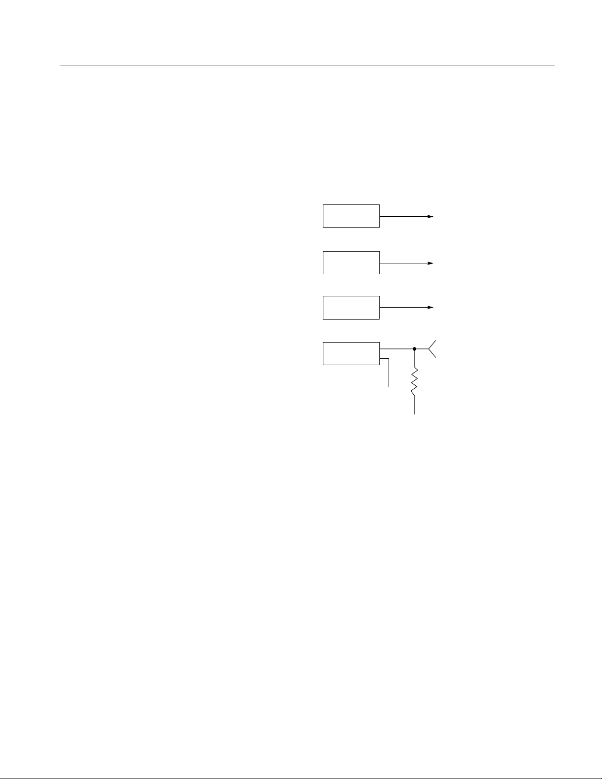
Probe Connectors and Signal Names 7. . . . . . . . . . . . . . . . . . . . . . . . . . . . . . . . .
Probe Overview 9. . . . . . . . . . . . . . . . . . . . . . . . . . . . . . . . . . . . . . . . . . . . . . . . .
Probe Dimensions 15. . . . . . . . . . . . . . . . . . . . . . . . . . . . . . . . . . . . . . . . . . . . . . . .
P6475 Installation Requirements 17. . . . . . . . . . . . . . . . . . . . . . . . . . . . . . . . . . . .
Input/Output Circuits 18. . . . . . . . . . . . . . . . . . . . . . . . . . . . . . . . . . . . . . . . . . . . .
Timing Diagrams 22. . . . . . . . . . . . . . . . . . . . . . . . . . . . . . . . . . . . . . . . . . . . . . . .
Specifications 25. . . . . . . . . . . . . . . . . . . . . . . . . . . . . . . . . . . . . . . . . . . . . . . . . . .
Maintenance
Functional Check 45. . . . . . . . . . . . . . . . . . . . . . . . . . . . . . . . . . . . . . . . . . . . . . . .
Inspection and Cleaning 45. . . . . . . . . . . . . . . . . . . . . . . . . . . . . . . . . . . . . . . . . . .
Static Discharge Information 45. . . . . . . . . . . . . . . . . . . . . . . . . . . . . . . . . . . . . . .
Configuring Probes 45. . . . . . . . . . . . . . . . . . . . . . . . . . . . . . . . . . . . . . . . . . . . . . .
Repackaging 49. . . . . . . . . . . . . . . . . . . . . . . . . . . . . . . . . . . . . . . . . . . . . . . . . . . .
TLA7PG2 Pattern Generator Probes Instruction Manual
i
Page 6

Table of Contents
List of Figures
Figure 1: Standard probe, lead sets, and probe cable 2. . . . . . . . . . . .
Figure 2: P6475 variable probe, lead sets, power cord,
and probe cable 3. . . . . . . . . . . . . . . . . . . . . . . . . . . . . . . . . . . . . . . . . . .
Figure 3: P6470 and P6474 output connector pin assignments 7. . . . .
Figure 4: P6471 output connector pin assignments 7. . . . . . . . . . . . . .
Figure 5: P6472 output connector pin assignments 8. . . . . . . . . . . . . .
Figure 6: P6473 output connector pin assignments 8. . . . . . . . . . . . . .
Figure 7: P6475 output connector pin assignments 8. . . . . . . . . . . . . .
Figure 8: Strobe output pulse pattern 11. . . . . . . . . . . . . . . . . . . . . . . . .
Figure 9: P6475 Variable probe output pulse pattern 11. . . . . . . . . . . .
Figure 10: P6475 CH6 output example 12. . . . . . . . . . . . . . . . . . . . . . . .
Figure 11: P6475 CH6 output mode pulse patterns 13. . . . . . . . . . . . . .
Figure 12: P6470, P6471, P6472, P6473 and P6474
probe dimensions 15. . . . . . . . . . . . . . . . . . . . . . . . . . . . . . . . . . . . . . . . . .
Figure 13: P6475 Variable probe dimensions 16. . . . . . . . . . . . . . . . . . .
Figure 14: P6470 input/output circuit 18. . . . . . . . . . . . . . . . . . . . . . . . .
Figure 15: P6471 input/output circuit 19. . . . . . . . . . . . . . . . . . . . . . . . .
Figure 16: P6472 input/output circuit 20. . . . . . . . . . . . . . . . . . . . . . . . .
Figure 17: Signaling sense 21. . . . . . . . . . . . . . . . . . . . . . . . . . . . . . . . . . .
Figure 18: P6474 input/output circuit 22. . . . . . . . . . . . . . . . . . . . . . . . .
Figure 19: Clock and strobe timing diagram 22. . . . . . . . . . . . . . . . . . .
Figure 20: P6470, P6472, P6473, and P6474 inhibit
timing diagram 23. . . . . . . . . . . . . . . . . . . . . . . . . . . . . . . . . . . . . . . . . . . .
Figure 21: P6470, P6472, P6473, and P6474 external event
for inhibit timing diagram 23. . . . . . . . . . . . . . . . . . . . . . . . . . . . . . . . . .
Figure 22: External event for jump timing diagram 23. . . . . . . . . . . . .
Figure 23: External event for half channel advance
timing diagram 24. . . . . . . . . . . . . . . . . . . . . . . . . . . . . . . . . . . . . . . . . . . .
Figure 24: External event for full channel advance
timing diagram 24. . . . . . . . . . . . . . . . . . . . . . . . . . . . . . . . . . . . . . . . . . . .
Figure 25: External event for delay to data output
for advance diagram 24. . . . . . . . . . . . . . . . . . . . . . . . . . . . . . . . . . . . . . .
ii
TLA7PG2 Pattern Generator Probes Instruction Manual
Page 7

Table of Contents
Figure 26: Removing the standard probe cover 46. . . . . . . . . . . . . . . . .
Figure 27: P6470 series termination resistors 47. . . . . . . . . . . . . . . . . . .
Figure 28: P6474 series termination resistors 48. . . . . . . . . . . . . . . . . . .
Figure 29: P6472 PECL and LVPECL jumper position 48. . . . . . . . . .
TLA7PG2 Pattern Generator Probes Instruction Manual
iii
Page 8

Table of Contents
List of Tables
Table 1: Inputs and outputs of pattern generator probes 9. . . . . . . .
Table 2: P6475 Variable probe installation requirements 17. . . . . . . . .
Table 3: P6470 TTL/CMOS probe 25. . . . . . . . . . . . . . . . . . . . . . . . . . .
Table 4: P6471 ECL probe 28. . . . . . . . . . . . . . . . . . . . . . . . . . . . . . . . .
Table 5: P6472 PECL/LVPECL probe 30. . . . . . . . . . . . . . . . . . . . . . . .
Table 6: P6473 LVDS probe 31. . . . . . . . . . . . . . . . . . . . . . . . . . . . . . . . .
Table 7: P6474 LVCMOS probe 34. . . . . . . . . . . . . . . . . . . . . . . . . . . . .
Table 8: P6475 Variable probe 37. . . . . . . . . . . . . . . . . . . . . . . . . . . . . .
Table 9: Power Supply (P6475 only) 42. . . . . . . . . . . . . . . . . . . . . . . . . .
Table 10: Atmospherics 42. . . . . . . . . . . . . . . . . . . . . . . . . . . . . . . . . . . .
Table 11: Dynamics characteristics (P6470, P6471,
P6472, P6473, P6474) 42. . . . . . . . . . . . . . . . . . . . . . . . . . . . . . . . . . . . . .
Table 12: Dynamics characteristics (P6475) 43. . . . . . . . . . . . . . . . . . . .
Table 13: Probe cables 43. . . . . . . . . . . . . . . . . . . . . . . . . . . . . . . . . . . . .
Table 14: Twisted lead set 43. . . . . . . . . . . . . . . . . . . . . . . . . . . . . . . . .
Table 15: Certifications and compliances for P6475 43. . . . . . . . . . . . .
Table 16: P6470 series termination resistors 47. . . . . . . . . . . . . . . . . . .
iv
TLA7PG2 Pattern Generator Probes Instruction Manual
Page 9

General Safety Summary
Review the following safety precautions to avoid injury and prevent damage to
this product or any products connected to it. To avoid potential hazards, use this
product only as specified.
Only qualified personnel should perform service procedures.
While using this product, you may need to access other parts of the system. Read
the General Safety Summary in other system manuals for warnings and cautions
related to operating the system.
To Avoid Fire or
Personal Injury
Use Proper Power Cord. Use only the power cord specified for this product and
certified for the country of use.
Ground the Product. These products (P6470, P6471, P6472, P6473, and P6474)
are indirectly grounded through the grounding conductor of the mainframe
power cord. The P6475 is directly grounded through the grounding conductor of
the probe power cord. To avoid electric shock, the grounding conductor must be
connected to earth ground. Before making connections to the input or output
terminals of the product, ensure that the product is properly grounded.
Observe All Terminal Ratings. To avoid fire or shock hazard, observe all ratings
and markings on the product. Consult the product manual for further ratings
information before making connections to the product.
Do Not Operate Without Covers. Do not operate this product with covers or panels
removed.
Use Proper Fuse. Use only the fuse type and rating specified for this product.
Avoid Exposed Circuitry. Do not touch exposed connections and components
when power is present.
Do Not Operate With Suspected Failures. If you suspect there is damage to this
product, have it inspected by qualified service personnel.
Do Not Operate in Wet/Damp Conditions.
Do Not Operate in an Explosive Atmosphere.
Keep Product Surfaces Clean and Dry.
Provide Proper Ventilation. Refer to the manual’s installation instructions for
details on installing the product so it has proper ventilation.
TLA7PG2 Pattern Generator Probes Instruction Manual
v
Page 10

General Safety Summary
Symbols and Terms
Terms in this Manual. These terms may appear in this manual:
WARNING. Warning statements identify conditions or practices that could result
in injury or loss of life.
CAUTION. Caution statements identify conditions or practices that could result in
damage to this product or other property.
Terms on the Product. These terms may appear on the product:
DANGER indicates an injury hazard immediately accessible as you read the
marking.
WARNING indicates an injury hazard not immediately accessible as you read the
marking.
CAUTION indicates a hazard to property including the product.
Symbols on the Product. The following symbols may appear on the product:
CAUTION
Refer to Manual
Protective Ground
(Earth) Terminal
vi
TLA7PG2 Pattern Generator Probes Instruction Manual
Page 11

Service Safety Summary
Only qualified personnel should perform service procedures. Read this Service
Safety Summary and the General Safety Summary before performing any service
procedures.
Do Not Service Alone. Do not perform internal service or adjustments of this
product unless another person capable of rendering first aid and resuscitation is
present.
Disconnect Power. To avoid electric shock, switch off the instrument power, then
disconnect the power cord from the mains power.
Use Care When Servicing With Power On. Dangerous voltages or currents may
exist in this product. Disconnect power, remove battery (if applicable), and
disconnect test leads before removing protective panels, soldering, or replacing
components.
To avoid electric shock, do not touch exposed connections.
TLA7PG2 Pattern Generator Probes Instruction Manual
vii
Page 12

General Safety Summary
viii
TLA7PG2 Pattern Generator Probes Instruction Manual
Page 13

Preface
Related Documentation
This document provides information on using and servicing the TLA7PG2
probes.
In addition to these probe instructions, the following documentation is available
for your Tektronix Logic Analyzer Family:
H The TLA7PG2 Pattern Generator and Probes Service Manual provides
service information for the pattern generator and pattern generator probes.
H The Tektronix Logic Analyzer Family User Manual provides overall user
information for the Tektronix logic analyzers.
H The online help provides information for the probes and pattern generator
user interfaces and the Pattern Generator Programmatic Interface (PPI).
H A series of instruction manuals for microprocessor support provides
operating and service instructions for the individual microprocessor support
packages that are available for use with the logic analyzer.
H Probe instructions accompany the logic analyzer modules to provide
operating and service information.
H The Tektronix Logic Analyzer Family Training Manual provides training
exercises to help you learn key features of the logic analyzer. The training
manual is designed to be used with the TLA7QS training board.
H A series of service manuals are available that provide performance verifica-
tion procedures and board-level service information for major components
of the logic analyzer.
TLA7PG2 Pattern Generator Probes Instruction Manual
ix
Page 14

Preface
Contacting Tektronix
Phone 1Ć800Ć833Ć9200*
Address Tektronix, Inc.
Department or name (if known)
14200 SW Karl Braun Drive
P.O. Box 500
Beaverton, OR 97077
USA
Web site www.tektronix.com
Sales support 1Ć800Ć833Ć9200, select option 1*
Service support 1Ć800Ć833Ć9200, select option 2*
Technical support Email: TechSupport@tektronix.com
1Ć800Ć833Ć9200, select option 3*
1Ć503Ć627Ć2400
6:00 a.m. - 5:00 p.m. Pacific time
* This phone number is toll free in North America. After office hours, please leave a
voice mail message.
Outside North America, contact a Tektronix sales office or distributor; see the
Tektronix web site for a list of offices.
x
TLA7PG2 Pattern Generator Probes Instruction Manual
Page 15

Operating Basics
Product Description
This section provides a brief description of the TLA7PG2 probes and information on connecting the probes from the pattern generator module to the target
system.
The pattern generator probes provide multichannel signals to simulate signals in
a test environment. Following are descriptions of the probes discussed in this
manual:
P6470 TTL/CMOS
P6471 ECL
P6472 PECL/LVPECL
P6473 LVDS
The P6470 provides TTL or CMOS signals to the target system and contains 16
data outputs, 1 clock output, and 1 strobe output. The V
adjustable from 2.0 V to 5.5 V. Figure 14 on page 18 shows the P6470 input/output circuit.
The P6470 probe comes standard with 75 termination resistors packs. You can
change the resistor packs to provide impedance matching for the target system.
Refer to Removing the Probe Cover on page 46 and Changing the Series
Termination Resistors on page 47.
The P6471 ECL pattern generator probe provides ECL signals to the target
system and contains 16 data outputs, 1 clock output, and 1 strobe output. Figure
15 on page 19 shows the P6471 input/output circuit.
The P6472 provides PECL/LVPECL signals to the target system and contains 8
data outputs, 1 clock output, and 1 strobe output. You can select PECL or
LVPECL by moving a jumper in the probe. See Configuring the P6472 for
PECL or LVPECL on page 48. Figure 16 on page 20 shows the P6472 input/output circuit.
The P6473 provides LVDS signals to the target system and contains 16 data
outputs, 1 clock output, and 1 strobe output. All inputs and outputs are LVDS
level.
output driver is
cc
P6474 LVCMOS
TLA7PG2 Pattern Generator Probes Instruction Manual
The P6474 provides LVCMOS signals to the target system and contains 16 data
outputs, 1 clock output and 1 strobe output. Figure 18 on page 22 shows the
P6474 input/output circuit.
V
The
of the output driver is adjustable from 1.2 V to 3.3 V.
cc
1
Page 16
Operating Basics
The P6474 comes standard with 75 termination resistors packs. You can
change the resistor packs to provide impedance matching for the target system.
Refer to Removing Probe the Cover on page 46 and Changing the Series
Termination Resistors on page 47.
P6475 Variable
The P6475 provides logic family signals such as ECL, TTL/CMOS, and
PECL/LVPECL and contains 8 data outputs and one clock output. The P6475
also supports variable delay (0 to 50 ns) for two channels (CH6 and CH7).
When using the P6475 probe with a P6470 (TTL/CMOS), P6473 (LVDS), or
P6474 (LVCMOS) probe, it is recommended that you use a Time Alignment
Cable (P/N 012-A223-00) in conjunction with the TLA7PG2 Pattern Generator
Module. The Time Alignment Cable ensures that the P6475 and the P6470,
P6473, or P6474 probes are time aligned and can be used together. Please order
one Time Alignment Cable (P/N 012-A223-00) for each P6470, P6473, and
P6474 probe.
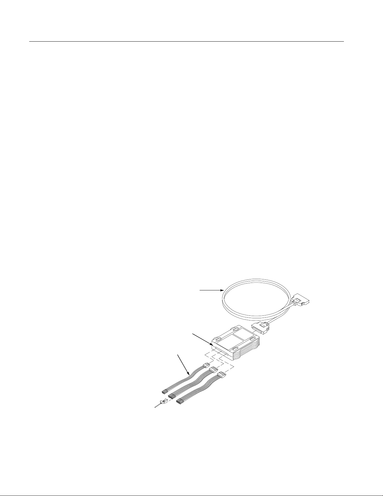
Probe Lead Sets and Cables
Figure 1 shows a typical pattern generator probe with the lead sets and probe
cable. The probe cable is included with the TLA7PG2 pattern generator module.
Refer to Probe Connectors and Signal Names, beginning on page 7, for probe
connector information.
Probe cable
Front panel
Lead sets
Figure 1: Standard probe, lead sets, and probe cable
2
TLA7PG2 Pattern Generator Probes Instruction Manual
Page 17
Front panel
Operating Basics
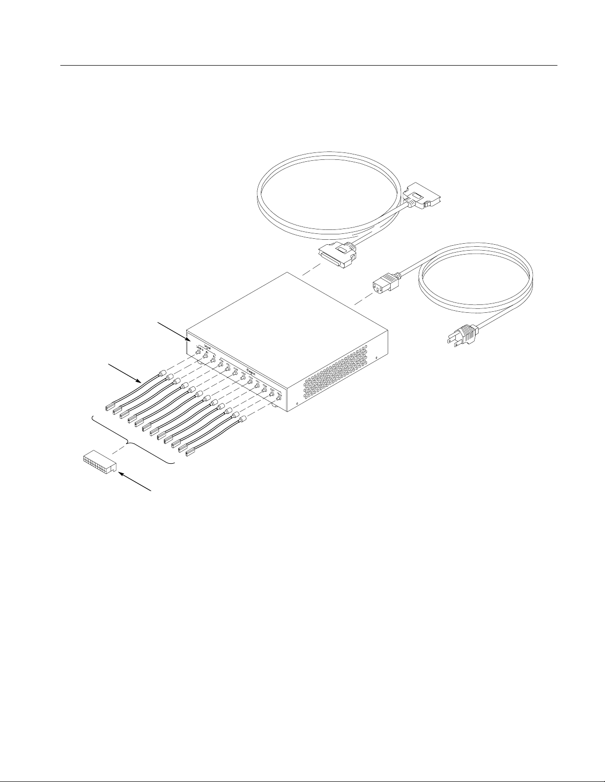
Figure 2 shows the P6475 variable probe, lead sets and probe cable. The probe
cable is included with the TLA7PG2 pattern generator module.
Lead sets
Note: The power
Connector
switch is located
on the rear panel
Figure 2: P6475 variable probe, lead sets, power cord, and probe cable
Connecting the Standard Probes
To connect the probes to the logic analyzer and to the target system, do the
following steps:
1. Power off the logic analyzer and the target system before connecting the
pattern generator probes.
2. Connect the lead sets to the target system.
3. Connect the standard probe as shown in Figure 1. The probe cable is
reversible. You can connect the probe cable in either direction.
TLA7PG2 Pattern Generator Probes Instruction Manual
3
Page 18
Operating Basics
4. Connect the probe to the pattern generator module on the logic analyzer.
CAUTION. To prevent damage to the pattern generator module or probe, do not
connect or disconnect the pattern generator cables to or from the pattern
generator module or probe while the logic analyzer is powered on. The
recommended DUT (Device Under Test) and pattern generator power on/off
sequence is as follows:
Power on the DUT first, then power on the pattern generator. Power off the
pattern generator and then power off the DUT.
Although the pattern generator probe cable appears to be a SCSI cable, it is not
compatible with a SCSI cable; do not use a SCSI cable with the pattern
generator module, or use the pattern generator probe cable with a SCSI
instrument.
The probe is fragile; handle it carefully.
Connecting the P6475 Probe
P6475 Connections
Do the following steps to connect the P6475 to the logic analyzer, the target
system, and to the power source:
1. Power off the logic analyzer and the target system before connecting the
pattern generator probes.
2. Connect the lead sets to the target system.
3. Connect the P6475 as shown in Figure 2. The probe cable is reversible;
either end can be connected to the P6475.
4. Connect the P6475 power cord.
5. Connect the probe to the pattern generator module on the logic analyzer.
4
TLA7PG2 Pattern Generator Probes Instruction Manual
Page 19

Operating Basics
Power On/Off
Follow the procedures below to power on and power off the P6475 variable
probe:
1. Power on the DUT
2. Power on the P6475
3. Power on the TLA
1. Power off the TLA
2. Power off the P6475
3. Power off the DUT
TLA7PG2 Pattern Generator Probes Instruction Manual
5
Page 20

Operating Basics
6
TLA7PG2 Pattern Generator Probes Instruction Manual
Page 21

Reference
This section provides reference information and specifications for the TLA7PG2
probes.
Probe Connectors and Signal Names
P6470 and P6474 Pin
Assignments
P6471 Pin Assignments
Figure 3 shows the P6470 TTL/CMOS and P6474 LVCMOS pin assignments on
the front panel.
A1 A0
765 43210 765 43210
GND
Top
Bottom
Figure 3: P6470 and P6474 output connector pin assignments
Figure 4 shows the P6471 ECL pin assignments on the front panel.
A1 A0
765 43210 765 43210
Top
Figure 4: P6471 output connector pin assignments
TLA7PG2 Pattern Generator Probes Instruction Manual
GND
Bottom
7
Page 22
Reference
P6472 Pin Assignments
P6473 Pin Assignments
Figure 5 shows the P6472 PECL/LVPECL pin assignments on the front panel.
A0
(not used)
765 43210
GND
Top
Bottom
Figure 5: P6472 output connector pin assignments
Figure 6 shows the P6473 LVDS pin assignments on the front panel.
A1 A0
765 43210 765 43210
Top
7 6 5 4 3 2 1 0 7 6 5 4 3 2 1 0
A1 A0
Figure 6: P6473 output connector pin assignments
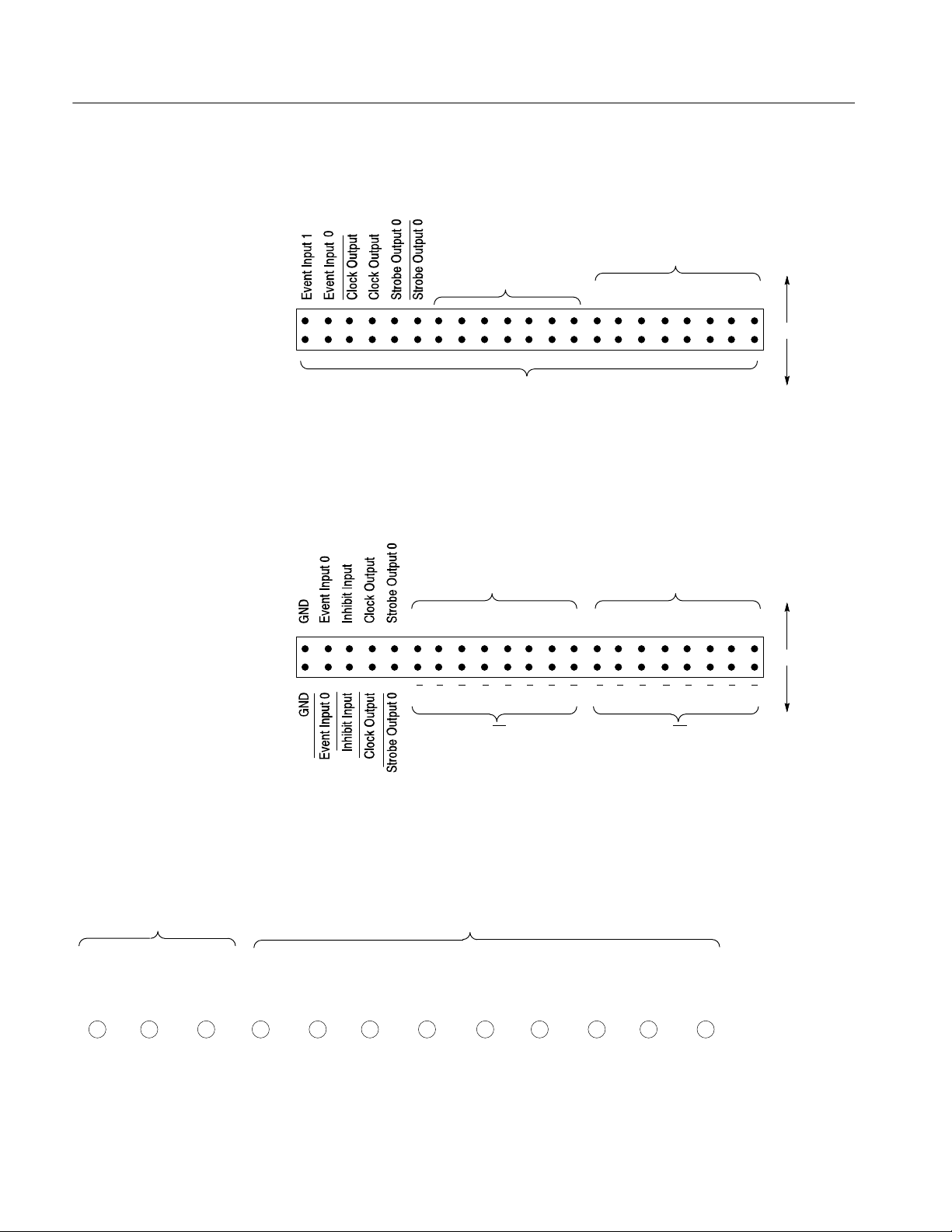
P6475 Pin Assignments
Input
Inhibit Event 0 Event 1 CH 0 CH 1 CH 2 CH 3 CH 4 CH 5 CH 7
Figure 7 shows the P6475 variable pin assignments on the front panel.
Output
Delay
Figure 7: P6475 output connector pin assignments
Bottom
ClockCH 6
Delay
8
TLA7PG2 Pattern Generator Probes Instruction Manual
Page 23

Probe Overview
Table 1 shows the signal names when used with different probes. These signal
names appear on the probe labels.
You can have up to four probes connected to each PG module. The leftmost
probe will be the master, and the probes to the right of the master are the slaves.
The probes are named Probe A, Probe B, Probe C, and Probe D, respectively.
Refer to Table 1 for input and output names for each probe.
Table 1: Inputs and outputs of pattern generator probes
Reference
P6470 TTL/
Characteristic
Data Output
(Full/Half)
Probe A A0 (0 through 7)
Probe B B0 (0 through 7)
Probe C C0 (0 through 7)
Probe D D0 (0 through 7)
CMOS
16/8 channels 16/8 channels 8/8 channels 16/8 channels 16/8 channels 8/8 channels
A1 (0 through 7)
B1 (0 through 7)
C1 (0 through 7)
P6471 ECL
A0 (0 through 7)
A1 (0 through 7)
B0 (0 through 7)
B1 (0 through 7)
C0 (0 through 7)
C1 (0 through 7)
D0 (0 through 7)
P6472 PECL/
LVPECL
A0 (0 through 7) A0 (0 through 7)
B0 (0 through 7) B0 (0 through 7)
C0 (0 through 7) C0 (0 through 7)
D0 (0 through 7) D0 (0 through 7)
P6473 LVDS P6474 LVCMOS P6475 Variable
A0 (0 through 7)
A1 (0 through 7)
A1 (0 through 7)
B0 (0 through 7)
B1 (0 through 7)
B1 (0 through 7)
C0 (0 through 7)
C1 (0 through 7)
C1 (0 through 7)
A0 (0 through 7)
A1 (0 through 7)
B0 (0 through 7)
B1 (0 through 7)
C0 (0 through 7)
C1 (0 through 7)
D0 (0 through 7)
A0 (0 through 7)
B0 (0 through 7)
C0 (0 through 7)
D0 (0 through 7)
D1 (0 through 7)
Clock Output 1
Probe A CLK CLK CLK, CLK CLK/CLK CLK CLK
Probe B CLK CLK CLK, CLK CLK/CLK CLK CLK
Probe C CLK CLK CLK, CLK CLK/CLK CLK CLK
Probe D CLK CLK CLK, CLK CLK/CLK CLK CLK
1
D1 (0 through 7)
1
1
D0 (0 through 7)
D1 (0 through 7)
D1 (0 through 7)
1
1
1
1
D1 (0 through 7)
1
1
TLA7PG2 Pattern Generator Probes Instruction Manual
1
9
Page 24

Reference
Table 1: Inputs and outputs of pattern generator probes (Cont.)
P6470 TTL/
Characteristic P6475 VariableP6474 LVCMOSP6473 LVDS
Strobe Output 1 1 1 1 1 0
Probe A STRB0 STRB0 STRB0, STRB0 STRB0/STRB0 STRB0
Probe B STRB1 STRB1 STRB1, STRB1 STRB2/STRB2 STRB1
Probe C STRB2 STRB2 STRB2, STRB2 STRB4/STRB4 STRB2
Probe D STRB3 STRB3 STRB3, STRB3 STRB6/STRB6 STRB3
Inhibit Input 1 0 0 1 1 1
Probe A INHB INHB/INHB INHB INHB
Probe B INHB INHB/INHB INHB INHB
Probe C INHB INHB/INHB INHB INHB
Probe D INHB INHB/INHB INHB INHB
Event Input
Probe A EVNT0, EVNT1 EVNT0, EVNT1 EVNT0, EVNT1 EVNT0/EVNT0 EVNT0, EVNT1 EVNT0, EVNT1
Probe B EVNT2, EVNT3 EVNT2, EVNT3 EVNT2, EVNT3 EVNT2/EVNT2 EVNT2, EVNT3 EVNT2, EVNT3
Probe C EVNT4, EVNT5 EVNT4, EVNT5 EVNT4, EVNT5 EVNT4/EVNT4 EVNT4, EVNT5 EVNT4, EVNT5
Probe D EVNT6, EVNT7 EVNT6, EVNT7 EVNT6, EVNT7 EVNT6/EVNT6 EVNT6, EVNT7 EVNT6, EVNT7
1
2
3
3
The Clock Output is disabled when Strobe Output is enabled.
CH6 and CH7 can be used as Strobe Outputs by setting the data format to RZ/R1.
The External Event Input is used to suspend/resume the sequencer (Advance function) or to jump to a
specified line in the sequence or inhibit the output.
CMOS
2 2 2 1 2 2
P6471 ECL
P6472 PECL/
LVPECL
2
10
Descriptions of the probe input and output control signals follow. For more
information on using the probe signals, refer to the online help for the pattern
generator.
Clock Output. Each probe has one clock output signal. The logic level of the
clock output is the same as the data output.
The clock output is disabled when the strobe output is enabled.
Strobe Output. Each probe has a strobe output signal except for the P6475
variable probe. CH 6and CH7 can be used as a strobe signal by setting the data
format to RZ/R1.
The logic level of the strobe output is the same as the data output.
The output format of the strobe is RZ (return to zero). The pulse width is the
same as the first or the second half of the clock cycle. The pulse can be
TLA7PG2 Pattern Generator Probes Instruction Manual
Page 25

Reference
positioned at either first half (Strobe delay: Zero) or second half (Strobe delay:
Trailing Edge) of the clock cycle.
Figure 8 shows the pulse pattern of the strobe output.
01
Strobe Data
Clock
RZ (firstĆhalf)
RZ (secondĆhalf)
Figure 8: Strobe output pulse pattern
P6475 Variable probe Output Format. Figure 9 shows the P6475 output pulse
patterns for various signals. NRZ is the output format for CH0 through CH5.
You can select NRZ, RZ, and R1 from CH6 and CH7. The delay pulse width
using RZ or R1 is equal to half of the clock cycle when using the internal clock
mode. The clock output polarity is selectable from Normal or Invert. Refer to the
TLA7PG2 for more information.
You can delay the CH6 and CH7 output up to 50 ns. Figure 9 shows the P6475
output pulse pattern.
0101
Data
Clock (normal)
Clock (invert)
NRZ
RZ
R1
Figure 9: P6475 Variable probe output pulse pattern
By using the CH6 Output Mode control, it is possible to output a wider or
narrower pulse from the CH6 output connector. Figure 11 shows the CH6 and
CH7 output pulse patterns when using the CH6 Output Mode control.
TLA7PG2 Pattern Generator Probes Instruction Manual
11
Page 26

Reference
For example, if the P6475 is setup as follows:
Clock Frequency: 100 MHz (10 ns period)
CH6: RZ, delay 3 ns
CH7: RZ, delay 5 ns
CH6 Output Mode: CH6 and CH7
The CH6 output will be as shown in Figure 10.
You will see an RZ pulse of 5 ns delay and a 3 ns width at the CH6 output
connector
CH0Ć6
CLK
CH6
CH7
CH6
Output
3 ns 5 ns
5 ns 5 ns
3 ns
Figure 10: P6475 CH6 output example
Figure 11 shows the various CH6 pulse patterns depending on which mode is
setup from the CH6 Output Mode Setup menu. See the TLA7PG2 Online Help
system for more information.
12
TLA7PG2 Pattern Generator Probes Instruction Manual
Page 27

Reference
Normal
CH6 or CH7
CH6 and CH7
CH6
CH7
CH6 Output
CH6
CH7
CH6 Output
CH6
CH7
CH6 Output
CH6 and (NOT CH7)
CH6
CH7
CH6 Output
Figure 11: P6475 CH6 output mode pulse patterns
Inhibit Input. The P6470, P6473, P6474 and P6475 have an inhibit input to set the
output to high impedance. The input polarity is positive true and a High input
will disable the output. Low input or no connection enables the output. The
P6475 input state (High or Low) with no connection will vary according to the
input threshold setting.
External Event Input. All of the probes have one or two event inputs. The pattern
generator detects an event when the external event input is High (True). The
external event input is Low (False) when no signal is detected or when the probe
TLA7PG2 Pattern Generator Probes Instruction Manual
13
Page 28

Reference
is not connected to the pattern generator. The P6475 input state (High or Low)
with no connection will vary according to the input threshold setting.
The external event can be used to Jump or Advance the sequencer or disable the
output. The input polarity is positive true.
Input Logic Level. All inputs are the same logic level as the output except for the
P6475 Variable probe. The V
of the input circuit is the same as the Vcc of the
cc
output driver for the P6470 TTL/CMOS probe and the P6474 LVCMOS probe.
The P6475 Variable probe input threshold level is adjustable within the range of
–2.5 V to +2.5 V.
14
TLA7PG2 Pattern Generator Probes Instruction Manual
Page 29

Probe Dimensions
Reference
Figure 12 shows the dimensions of the standard pattern generator probes. The
physical dimensions are the same for the P6470, P6471, P6472, P6473, and
P6474 probes.
NOTE. There are no ventilation requirements for the standard probes.
137.2 mm
(5.402 in)
114.0 mm
(4.488 in)
130.0 mm
(5.118 in)
33.0 mm
(1.299 in)
Probe weight : 250 g (8.8 oz)
Figure 12: P6470, P6471, P6472, P6473 and P6474 probe dimensions
TLA7PG2 Pattern Generator Probes Instruction Manual
15
Page 30

Reference
Figure 13 shows the dimensions of the P6475 probe.
250.0 mm
(9.843 in)
250.0 mm
(9.843 in)
55.55 mm
(2.185 in)
Figure 13: P6475 Variable probe dimensions
16
TLA7PG2 Pattern Generator Probes Instruction Manual
Page 31

P6475 Installation Requirements
Table 2 provides information for the P6475 Variable probe installation:
Table 2: P6475 Variable probe installation requirements
Characteristics Description
Maximum power dissipation
(fully loaded)
Surge Current Max 57 A peak (25° C) ≤ 5 line cycles after product has been
Clearance for ventilation
Side 10 cm (3.9 in)
35 W max. Maximum line current is 0.6 A
90 V line, with 5 % clipping
turned off for at least 30 s
at 50 Hz,
rms
Reference
TLA7PG2 Pattern Generator Probes Instruction Manual
17
Page 32

Reference
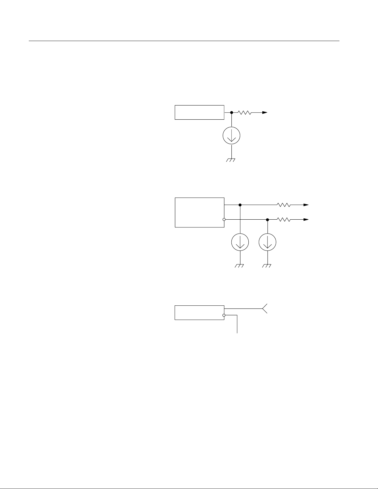
Input/Output Circuits
This subsection shows the input/output circuits for the P6470, P6471, P6472,
P6473. and P6474 probes.
P6470
Figure 14 shows the probe input/output circuit for the P6470 TTL/CMOS pattern
generator probe. The P6470 comes standard with 75
resistor packs. You can
change the resistor packs to provide impedance matching for the target system.
The P6470 provides 16 data outputs, 1 clock output, and 1 strobe output.
75
Data Output
Clock/Strobe Output
Event/Inhibit Input
74LVC541A
75
74LVC244A
74LVC14A
1 k
18
GND
Figure 14: P6470 input/output circuit
TLA7PG2 Pattern Generator Probes Instruction Manual
Page 33
Reference
P6471
Figure 15 shows the probe input/output circuit for the P6471 ECL pattern
generator probe.
The P6471 provides 16 data outputs, 1 clock output, and 1 strobe output.
Data Output
Strobe Output
Clock Output
Event Input
100E151
100EL16
100EL04
10H116
75 k
V
BB
Figure 15: P6471 input/output circuit
-2 V
TLA7PG2 Pattern Generator Probes Instruction Manual
19
Page 34
Reference
P6472
Figure 16 shows the input/output circuit for the P6472 PECL/LVPECL pattern
generator probe. The P6472 provides PECL/LVPECL signals to the target
system and contains 8 data outputs, 1 clock output, and 1 strobe output.
43
Data Output
100EP90
100EP90Clock/Strobe Output
10 mA
10 mA
43
43
10 mA
20
Event Input
100EL91
Figure 16: P6472 input/output circuit
TLA7PG2 Pattern Generator Probes Instruction Manual
VBB
Page 35

Reference
P6473
The P6473 LVDS is compatible with the TIA/EIA-644 standard.
A generator circuit in the probe produces a balanced source that results in a
differential voltage across a test termination load of 100
in the range of
250 mV to 450 mV.
Figure 17 illustrates the signaling sense of the voltages appearing across the
termination resistor.
H The A terminal of the generator is negative with respect to the B terminal for
a binary 1 or OFF state.
H The A terminal of the generator is positive with respect to the B terminal for
a binary 0 or ON state.
1
OFF
VB
A
B
Z =100
t
G
C
VA
VA ĆVB
ON
0
1
OFF
+1.2 V typical
+250 mV to +400 mV
0 V (Diff)
-250 mV to -400 mV
Figure 17: Signaling sense
TLA7PG2 Pattern Generator Probes Instruction Manual
21
Page 36

Reference
P6474
Figure 18 shows the input/output circuit for the P6474 LVCMOS pattern
generator probe. The P6474 provides LVCMOS signals to the target system and
contains 16 data outputs, one clock output and one strobe output. You can adjust
the V
P6474 comes standard with 75
of the output driver and the input receiver from 1.2 V to 3.3 V. The
cc
resistor packs. You can change the resistor
packs to provide impedance matching for the target system.
The P6474 provides 16 data outputs, 1 clock output and 1 strobe output.
Data/Clock/Strobe Output
Event/Inhibit Input
74AVC16244
74AVC16244
75
1k
Figure 18: P6474 input/output circuit
Timing Diagrams
Figures 19 through 24 show the pattern generator timing diagrams. The diagrams
apply to all probes unless otherwise stated.
External clock Input
Td1
Clock Output
Td2
Data Output
Td3
Strobe Output
(strobe delay = zero)
Figure 19: Clock and strobe timing diagram
22
TLA7PG2 Pattern Generator Probes Instruction Manual
Page 37

Inhibit Input or
Probe D data Output
Td4
Data Output
Figure 20: P6470, P6472, P6473, and P6474 inhibit timing diagram
Reference
Td5
10%
90%
Event
Input
Td6
Clock
Output
Data
Output
Td6
Figure 21: P6470, P6472, P6473, and P6474 external event for inhibit timing diagram
Event Input
Td9
Data Output Current Block Jump Target Block
Figure 22: External event for jump timing diagram
TLA7PG2 Pattern Generator Probes Instruction Manual
23
Page 38

Reference
Event
Input
Td10
Clock
Output
End of previous block
Figure 23: External event for half channel advance timing diagram
Event
Input
Td11
Clock
Output
End of previous block Block Output
Figure 24: External event for full channel advance timing diagram
Block Output
after the event
after the event
24
Event
Input
Td12
Clock
Output
Block Output
after the event
Figure 25: External event for delay to data output for advance diagram
TLA7PG2 Pattern Generator Probes Instruction Manual
Page 39

Specifications
load: 10 k
8
The specifications apply to all versions of the pattern generator unless otherwise
noted.
Table 3: P6470 TTL/CMOS probe
All timing values are specified at the probe connector under the conditions listed below, unless otherwise noted:
Output Voltage setting: +5 V
Series Termination Resistor: 75
Load: 510 + 50 pF
Characteristic Description
Maximum Clock Frequency
(with series termination resistor: 75 )
Output Level (Vcc) Full Channel mode Half Channel mode
Vcc v 3.3 V 134 MHz 268 MHz
3.3 V < Vcc v5 V 62.5 MHz 125 MHz
Vcc > 5 V 52.5 MHz 105 MHz
Reference
Maximum Clock Frequency
(with series termination resistor: 75 ,
+ 15 pf, sample output pattern:
bit counter)
Typical
Output Level (VCC) 2.0 V to 5.5 V, 25 mV step, into 1 M
Maximum Resistive Load 220
Maximum Capacitive Load 50 pF
Output Type 74LVC541A for Data Output
Series Termination Resistor 75 standard. 43, 100 and 150 as optional accessories
Supported Channel Mode Half and Full
Number of External Inhibit Inputs 1
Rise/Fall Time
(20% to 80%
load: 1 M +< 1 pF)
Typical
Rise/Fall Time
(20% to 80%
load: 510 + 51 pF)
Typical
Output Level (Vcc) Full Channel mode Half Channel mode
Vcc v5.5 V 134 MHz 268 MHz
74LVC244A for Clock/Strobe Output
(18 pin DIP socket)
Clock/Strobe Output
Rise 640 ps
Fall 1.1 ns
Data Output
Rise 680 ps
Fall 2.9 ns
Clock/Strobe Output
Rise 6.5 ns
Fall 6.3 ns
Data Output
Rise 5.2 ns
Fall 4.5 ns
TLA7PG2 Pattern Generator Probes Instruction Manual
25
Page 40

Reference
Table 3: P6470 TTL/CMOS probe (Cont.)
All timing values are specified at the probe connector under the conditions listed below, unless otherwise noted:
Output Voltage setting: +5 V
Series Termination Resistor: 75
Load: 510 + 50 pF
Characteristic Description
Data Output Skew
Typical
< 570 ps between all data output pins of all modules in the mainframe after
intermodule skew is adjusted manually
< 480 ps between all data output pins of all probes of single module
< 440 ps between all data output pins of single probe
Data Output to Strobe Output Delay
Typical
Data Output to Clock Output Delay
Typical
External Clock Input to Clock Output Delay
Typical
External Inhibit Input to Output Enable Delay
Typical
External Inhibit Input to Output Disable Delay
Typical
Probe D Data Output to Output Enable Delay
(for Internal Inhibit) Typical
Probe D Data Output to Output Disable Delay
(for Internal Inhibit) Typical
External Event Input to Clock Output Setup
(for inhibit)
(eventĆfilter: off) Typical
External Event Input and Inhibit Input
Input Type
Minimum Pulse Width
External Event Input Delay to Data Output for
Advance
+ 1.7 ns when strobe delay set to zero. (Td3 in Figure 19 on page 22)
+2.4 ns (Td2 in Figure 19 on page 22)
61 ns (Td1 in Figure 19 on page 22)
34 ns for Data Output (Td4 in Figure 20 on page 23)
86 ns for Data Output (Td5 in Figure 20 on page 23)
7 ns for Data Output (Td4 in Figure 20 on page 23)
8 ns for Data Output (Td5 in Figure 20 on page 23)
Full channel mode: 1.5 clocks + 240 ns (Td6 in Figure 21 on page 23)
Half channel mode: 2 clocks + 240 ns
74LVC14A, Positive True, 1 k to GND
200 ns (event filter: off)
230 ns to 330 ns + 1.5 to 2.5 CLK2 (Td12 in Figure 25 on page 24)
(CLK2 is from 2.5 ns to 5 ns when Internal Clock is used. It is the same as one clock
period when the External Clock is used.)
External Event Input
Number of Inputs
Setup Time of Event Typical
Input for Event Jump
26
2
Half Channel Mode
54 to 61 clocks + 240 ns before the next block
Full Channel Mode
27.5 to 31 clocks + 240 ns before the next block
(Td9 in Figure 22 on page 23)
TLA7PG2 Pattern Generator Probes Instruction Manual
Page 41

Table 3: P6470 TTL/CMOS probe (Cont.)
All timing values are specified at the probe connector under the conditions listed below, unless otherwise noted:
Output Voltage setting: +5 V
Series Termination Resistor: 75
Load: 510 + 50 pF
Characteristic Description
Setup Time of Event Input for Event Advance
Typical
Mainframe External Signal Input to PG Probe
data output
for Advance
via Signal 1, 2 Typical
via Signal 3, 4 Typical
for Inhibit
via Signal 1, 2 Typical
In Half Channel Mode, 240 ns before the rising edge of 5th clock output pulse from
the last of the previous block (Td10 in Figure 23 on page 24)
In Full Channel Mode, 240 ns before the rising edge of 3rd clock output pulse from the
last of the previous block (Td11 in Figure 24 on page 24)
200 ns to 300 ns + 1.5 to 2.5 CLK2
230 ns to 330 ns + 1.5 to 2.5 CLK2
(CLK2 is from 2.5 ns to 5 ns when the Internal Clock is used. It is the same as one
clock period when the External Clock is used)
100 ns to 200 ns + 2 to 3 CLK (Half Channel Mode)
100 ns to 200 ns + 1.5 to 2.5 CLK (Full Channel Mode)
Reference
via Signal 3, 4 Typical
PG Probe Clock Output to Mainframe External
Signal Output
via Signal 1, 2 Typical
via Signal 3, 4 Typical
Number of Data Outputs 16 in Full Channel Mode
Number of Clock Outputs 1
Number of Strobe Outputs 1
Number of External Event Inputs 2
Clock Output Polarity Positive
Strobe Type RZ only
130 ns to 230 ns+ 2 to 3 CLK (Half Channel Mode)
130 ns to 230 ns + 1.5 to 2.5 CLK (Full Channel Mode)
18 ns - 5 CLK (Half Channel Mode)
18 ns - 3 CLK (Full Channel Mode)
29 ns - 5 CLK (Half Channel Mode)
29 ns - 3 CLK (Full Channel Mode)
8 in Half Channel Mode
(Only one Clock Output or Strobe Output can be enabled at one time per probe)
TLA7PG2 Pattern Generator Probes Instruction Manual
27
Page 42

Reference
Table 4: P6471 ECL probe
All timing values are specified at the probe connector under the condition listed below, unless otherwise noted:
Load: 51 terminated to -2 V
Characteristic Description
Maximum Clock Frequency 134 MHz in Full Channel mode
268 MHz in Half Channel mode
Output Level ECL
Output Type 100E151 for data output
100EL16 for strobe output
100EL04 for clock output
outputs are unterminated
Supported Channel Mode Half and Full
Rise/Fall Time
(20% to 80%) Typical
Data Output Skew Typical < 255 ps between all data output pins of all modules in the mainframe after
Data Output to Strobe Output Delay
Typical
Data Output to Clock Output Delay
Typical
External Clock Input to Clock Output Delay
Typical
External Event Input Delay to Data Output for
Advance
Clock Output
Rise 320 ps
Fall 330 ps
Data Output
Rise 1,200 ps
Fall 710 ps
Strobe Output
Rise 290 ps
Fall 270 ps
intermodule skew is adjusted manually
< 240 ps between all data output pins of all probes of single module
< 210 ps between all data output pins of a single probe
+2.94 ns when strobe delay set to zero (Td3 in Figure 19 on page 22)
+780 ps (Td2 in Figure 19 on page 22)
50 ns (Td1 in Figure 19 on page 22)
170 ns to 270 ns + 1.5 to 2.5 CLK2 (Td12 in Figure 25 on page 24)
(CLK2 is from 2.5 ns to 5 ns when Internal Clock is used. It is the same as one clock
period when the External Clock is used.)
External Event Input
Input Level
Input Type
Minimum Pulse Width
External Event Input
Number of Inputs
Setup Time of Event
Input for Event Jump
Typical
28
ECL
10H116 with 75 k to -2 V
150 ns (Event filter: off)
2
Half Channel Mode, 54 to 61 clocks + 180 ns before the next block
Full Channel Mode, 27.5 to 31 clocks + 180 ns before the next block (Td9 in Figure 22
on page 23)
TLA7PG2 Pattern Generator Probes Instruction Manual
Page 43
Table 4: P6471 ECL probe (Cont.)
All timing values are specified at the probe connector under the condition listed below, unless otherwise noted:
Load: 51 terminated to -2 V
Characteristic Description
Setup Time of Event
Input for Event Advance
Typical
Mainframe External Signal Input to PG Probe
data output
for Advance
via Signal 1, 2 Typical
via Signal 3, 4 Typical
Half Channel Mode:
80 ns before the rising edge of 5th clock output pulse from the last of the
previous block (Td10 in Figure 23 on page 24)
Full Channel Mode
80 ns before the rising edge of 3rd clock output pulse from the last of the
previous block (Td11 in Figure 24 on page 24)
200 ns to 300 ns + 1.5 to 2.5 CLK2
230 ns to 330 ns + 1.5 to 2.5 CLK2
(CLK2 from 2.5 ns to 5 ns when Internal Clock is used. It is same as one clock period
when External Clock is used.)
Reference
PG Probe Clock Output to Mainframe External
Signal Output
via Signal 1, 2 Typical
via Signal 3, 4 Typical
Number of Data Outputs 16 in Full Channel Mode
Number of Clock Outputs 1
Number of Strobe Outputs 1
Number of External Event Inputs 2
Clock Output Polarity Positive
Strobe Type RZ only
28 ns - 5 CLK (Half Channel Mode)
28 ns - 3 CLK (Full Channel Mode)
38 ns - 5 CLK (Half Channel Mode)
38 ns - 3 CLK (Full Channel Mode)
8 in Half Channel Mode
(Only one Clock Output or one Strobe Output can be enabled at one time per probe)
TLA7PG2 Pattern Generator Probes Instruction Manual
29
Page 44

Reference
qy
Table 5: P6472 PECL/LVPECL probe
All timing values are specified with a load condition of 1 M + ≤ 1 pF with PECL mode.
Characteristic Description
Maximum Clock Frequency Full Channel Mode Half Channel Mode
134 MHz 268 MHz
Number of Data Outputs 8 Full Channel
8 Half Channel
Number of Clock Outputs 1 differential
Number of Strobe Outputs 1 differential
(Only one Clock Output or one Strobe Output can be enabled at one time per probe)
Number of External Event Inputs 2
Clock Output Polarity Positive
Strobe Type RZ (return to zero) only
Strobe Delay Zero or Trailing Edge
Output Level PECL, LVPECL (selectable by moving a jumper in the probe)
Output Type 100EL90 (all outputs are terminated)
Supported Channel Mode Half and Full
Rise/Fall Time (20% to 80%) Rise 430 ps
Fall 970 ps
Data Output Skew < 385 ps between all data output pins of all modules in the mainframe after
intermodule skew is adjusted manually
< 370 ps between all data output pins of all probes of single module
< 340 ps between all data output pins of a single probe
Data Output to Strobe Output Delay + 2.93 ns when strobe delay is set to zero (See Td3 in Figure 19 on page 22)
Data Output to Clock Output Delay + 1.12 ns (Td2 in Figure 19 on page 22)
External Clock Input to Clock Output Delay 50 ns (See Td1 in Figure 19 on page 22)
External Event Input Delay to Data Output for
Advance
External Event Input
Input Level
Input Type
Minimum Pulse Width (event filter: off)
170 ns to 270 ns + 1.5 to 2.5 CLK2 (Td12 in Figure 25 on page 24)
(CLK2 is from 2.5 ns to 5 ns when Internal Clock is used. It is the same as one clock
period when the External Clock is used.)
PECL, LVPECL (selectable by moving a jumper in the probe)
100EL91, unterminated
150 ns
30
TLA7PG2 Pattern Generator Probes Instruction Manual
Page 45
Table 5: P6472 PECL/LVPECL probe (Cont.)
Using signa
Using signal 1 or 2
qy
All timing values are specified with a load condition of 1 M + ≤ 1 pF with PECL mode.
Characteristic Description
External Event Input
Reference
Setup Time of Event Input for Event
Jump
Setup Time of Event Input for Event Advance Half Channel Mode: 180 ns before the rising edge of the 5th clock output pulse from
Mainframe External Signal Input to PG Probe
Data Output
For Advance:
l 1 or 2
Using signal 3 or 4
PG Probe Clock Output to Mainframe External
Signal Output
Using signal 1 or 2
Half Channel Mode: 54 to 61 Clocks + 180 ns before the next block
Full Channel Mode: 27.5 to 31 Clocks + 180 ns before the next block
(see Td9 in Figure 22 on page 23)
the last of the previous block (See Td10 in Figure 23 on page 24)
Full Channel Mode: 180 ns before the rising edge of the 3rd clock output pulse from
the last of the previous block (see Td11 in Figure 24 on page 24)
200 ns to 300 ns + 1.5 to 2.5 CLK2
230 ns to 330 ns + 1.5 to 2.5 CLK2
(CLK2 is from 2.5 ns to 5 ns when Internal Clock is used. It is the same as one clock
period when the External Clock is used.)
31 ns -5 CLK (Half Channel Mode)
31 ns -3 CLK (Full Channel Mode)
Using signal 3 or 4
40 ns -5 CLK (Half Channel Mode)
40 ns -3 CLK (Full Channel Mode)
Table 6: P6473 LVDS probe
All timing values are specified at the probe connector under the condition listed below, unless otherwise noted:
Load: 100 + < 1 pF
Characteristic Description
Maximum Clock Frequency Full Channel Mode Half Channel Mode
134 MHz 268 MHz
Number of Data Outputs 16 Full Channel
8 Half Channel
TLA7PG2 Pattern Generator Probes Instruction Manual
31
Page 46
Reference
Table 6: P6473 LVDS probe (Cont.)
All timing values are specified at the probe connector under the condition listed below, unless otherwise noted:
Load: 100 + < 1 pF
Characteristic Description
Number of Clock Outputs 1 (Only one Clock Output or One Strobe Output can be enabled at one time per
probe.)
Number of Strobe Outputs 1 (Only one Clock Output or One Strobe Output can be enabled at one time per
probe.)
Number of External Event Inputs 1
Number of External Inhibit Inputs 1
Clock Output Polarity Positive
Strobe Type RZ (return to zero) only
Strobe Delay Zero or Trailing Edge
Maximum Capacitive Load 10 pF
Output Type LVDS (TIA/EIA-644 compatible)
Supported Channel Mode Half and Full
Rise/Fall Time
Rise: 910 ps
(20% to 80%)
Data Output Skew < 365 ps between all data output pins of all modules in the mainframe after
Data Output to Strobe Output Delay -280 ns when strobe delay is set to zero (See Td3 in Figure 19 on page 22)
Data Output to Clock Output Delay 1.2 ns (Td2 in Figure 19 on page 22)
External Clock Input to Clock Output Delay 55 ns (See Td1 in Figure 19 on page 22 )
External Inhibit Input to Output Enable Delay 9 ns for Data Output (See Td4 in Figure 20 on page 23)
External Inhibit Input to Output Disable Delay 12 ns for Data Output (See Td5 in Figure 20 on page 23)
Probe D Data Output to Output Enable Delay
(for Internal Inhibit)
Probe D Data Output to Output Disable Delay
(for Internal Inhibit)
External Event Input to Clock Output Setup
(for inhibit) eventĆfilter: off
External Event Input Delay to Data Output for
Advance
Fall: 750 ps
intermodule skew is adjusted manually
< 350 ps between all data output pins of all probes of single module
< 320 ps between all data output pins of a single probe
2 ns for Data Output (See Td4 in Figure 20 on page 23)
5 ns for Data Output (See Td5 in Figure 20 on page 23)
Full Channel mode: 1.5 Clocks + 180 ns
Half Channel mode: 2 Clocks + 180 ns
(See Td6 in Figure 21 on page 23)
170 ns to 270 ns + 1.5 to 2.5 CLK2 (Td12 in Figure 25 on page 24)
(CLK2 is from 2.5 ns to 5 ns when Internal Clock is used. It is the same as one clock
period when the External Clock is used.)
32
TLA7PG2 Pattern Generator Probes Instruction Manual
Page 47
Table 6: P6473 LVDS probe (Cont.)
All timing values are specified at the probe connector under the condition listed below, unless otherwise noted:
Load: 100 + < 1 pF
Characteristic Description
External Event Input and Inhibit Input
Reference
Input Type
Minimum Pulse Width (event filter: off)
External Event Input Setup Time of Event
Input for Event Jump
External Event Input Setup Time for Event
Advance
Mainframe External Signal Input to PG Probe
Data Output
For Advance:
Using signal 1 or 2
Using signal 3 or 4
For Inhibit:
LVDS (TIA/EIA-644 compatible), positive true
150 ns
Half Channel Mode: 54 to 61 Clocks + 180 ns before the next block
Full Channel Mode: 27.5 to 31 Clocks + 180 ns before the next block
(See Td9 in Figure 22 on page 23)
Half Channel Mode: 180 ns before the rising edge of the 5th clock output pulse from
the last of the previous block (See Td10 in Figure 23 on page 24)
Full Channel Mode: 180 ns before the rising edge of the 3rd clock output pulse from
the last of the previous block (See Td11 in Figure 24 on page 24)
200 ns to 300 ns + 1.5 to 2.5 CLK2
230 ns to 330 ns + 1.5 to 2.5 CLK2
(CLK2 is from 2.5 ns to 5 ns when Internal Clock is used. It is the same as one clock
period when the External Clock is used.)
Using signal 1 or 2
Using signal 3 or 4
PG Probe Clock Output to Mainframe External
Signal Output
Using signal 1 or 2
Using signal 3 or 4
100 ns to 200 ns + 2 to 3 CLK (Half Channel Mode)
100 ns to 200 ns +1.5 to 2.5 CLK (Full Channel Mode)
130 ns 230 ns + 2 to 3 CLK (Half Channel Mode)
130 ns to 230 ns + 1.5 to 2.5 CLK (Full Channel Mode)
26 ns -5 CLK (Half Channel Mode)
26 ns -3 CLK (Full Channel Mode)
35 ns -5 CLK (Half Channel Mode)
35 ns -3 CLK (Full Channel Mode)
TLA7PG2 Pattern Generator Probes Instruction Manual
33
Page 48
Reference
qy
Table 7: P6474 LVCMOS probe
All timing values are specified at the probe connector under the conditions listed below, unless otherwise noted:
Output Voltage setting: +3.3 V
Series Termination Resistor: 75
Load: 510 pF
Characteristic Description
Maximum Clock Frequency Full Channel Mode Half Channel Mode
134 MHz 268 MHz
Number of Data Outputs 16 Full Channel
8 Half Channel
Number of Clock Outputs 1 (Only one Clock Output or One Strobe Output can be enabled at one time per
probe.)
Number of Strobe Outputs 1 (Only one Clock Output or One Strobe Output can be enabled at one time per
probe.)
Number of External Event Inputs 2
Number of External Inhibit Inputs 1
Clock Output Polarity Positive
Strobe Type RZ (return to zero) only
Strobe Delay Zero or Trailing Edge
Output Level (Vcc) 1.2 V to 3.3 V, 25 mV step, into 1 M
Maximum Resistive Load 510
Maximum Capacitive Load 20 pF
Output Type 74AVC16244
Series Termination Resistor 75 standard. 43, 100 and 150 as optional accessories
(18 pin DIP socket)
Supported Channel Mode Half and Full
Rise/Fall Time
Rise 1200 ps
(20 % to 80 %, load: 1M < 1 pF)
Rise/Fall Time
(20 % to 80 %, load: 510 50 pF)
Data Output Skew < 590 ps between all data output pins of all modules in the mainframe after
Data Output to Strobe Output Delay 460 ps when strobe delay is set to zero (See Td3 in Figure 19 on page 22)
Data Output to Clock Output Delay 1.84 ns (Td2 in Figure 19 on page 22)
External Clock Input to Clock Output Delay 55 ns (See Td1 in Figure 19 on page 22)
34
Fall 610 ps
Rise 3.4 ns
Fall 3.2 ns
intermodule skew is adjusted manually
< 500 ps between all data output pins of all probes of single module
< 460 ps between all data output pins of a single probe
TLA7PG2 Pattern Generator Probes Instruction Manual
Page 49

Table 7: P6474 LVCMOS probe (Cont.)
All timing values are specified at the probe connector under the conditions listed below, unless otherwise noted:
Output Voltage setting: +3.3 V
Series Termination Resistor: 75
Load: 510 pF
Characteristic Description
External Inhibit Input to Output Enable Delay 36 ns for Data Output (See Td4 in Figure 20 on page 22)
External Inhibit Input to Output Disable Delay 18 ns for Data Output (See Td5 in Figure 20 on page 22)
Probe D Data Output to Output Enable Delay
(for Internal Inhibit)
Probe D Data Output to Output Disable Delay
(for Internal Inhibit)
External Event Input to Clock Output Setup
(for inhibit) eventĆfilter: off
6 ns for Data Output (See Td4 in Figure 20 on page 22)
7 ns for Data Output (See Td5 in Figure 20 on page 22)
Full Channel mode: 1.5 Clocks + 180 ns
Half Channel mode: 2 Clocks + 180 ns
Reference
External Event Input Delay to Data Output for
Advance
External Event Input and Inhibit Input
Input Type
Minimum Pulse Width
External Event Input
Setup Time of Event
Input for Event Jump
External Event Input Setup Time for Event
Advance
(See Td6 in Figure 21 on page 23)
170 ns to 270 ns + 1.5 to 2.5 CLK2 (Td12 in Figure 25 on page 24)
(CLK2 is from 2.5 ns to 5 ns when Internal Clock is used. It is the same as one clock
period when the External Clock is used.)
74AVC16244, Positive True, 1 k to GND
The Vcc of the input receiver is variable and the same as the Vcc of the output driver.
150 ns (event filter: off)
Half Channel Mode: 54 to 61 Clocks + 180 ns before the next block
Full Channel Mode: 27.5 to 31 Clocks + 180 ns before the next block
(See Td9 in Figure 22 on page 23)
Half Channel Mode: 180 ns before the rising edge of the 5th clock output pulse from
the last of the previous block (See Td10 in Figure 23 o n page 24)
Full Channel Mode: 180 ns before the rising edge of the 3rd clock output pulse from
the last of the previous block (See Td11 in Figure 24 on page 24)
TLA7PG2 Pattern Generator Probes Instruction Manual
35
Page 50

Reference
(
(CLK2 is from 2.5 ns to 5 ns when the Internal Clock is used. It is the same as one
Table 7: P6474 LVCMOS probe (Cont.)
All timing values are specified at the probe connector under the conditions listed below, unless otherwise noted:
Output Voltage setting: +3.3 V
Series Termination Resistor: 75
Load: 510 pF
Characteristic Description
Mainframe External Signal Input to PG Probe
Data Output
For Advance:
Using signal 1 or 2
Using signal 3 or 4
For Inhibit:
Using signal 1 or 2
Using signal 3 or 4
PG Probe Clock Output to Mainframe External
Signal Output
Using signal 1 or 2
Using signal 3 or 4
200 ns to 300 ns + 1 to 2 CLK2
230 ns to 330 ns + 1 to 2 CLK2
CLK2 is from 2.5 ns to 5 ns when the Internal Clock is used. It is the same as one
clock period when the External Clock is used.)
100 ns to 200 ns + 2 to 3 CLK (Half Channel Mode)
100 ns to 200 ns + 1.5 to 2.5 CLK (Full Channel Mode)
130 ns to 230 ns + 2 to 3 CLK (Half Channel Mode)
130 ns to 230 ns + 1.5 to 2.5 CLK (Full Channel Mode)
25 ns -5 CLK (Half Channel Mode)
25 ns -3 CLK (Full Channel Mode)
34 ns -5 CLK (Half Channel Mode)
34 ns -3 CLK (Full Channel Mode)
36
TLA7PG2 Pattern Generator Probes Instruction Manual
Page 51

Table 8: P6475 Variable probe
Vol
-3 V to +6.75, 10 mV step, into 1 M
All timing values are specified at the probe connector under the conditions listed below, unless otherwise noted:
Output Voltage setting: Voh +2 V, Vol 0 V
Slew Rate: 2.5 V/ns
Delay Range: 0
Delay Time: 0 ns
Load: 50
Characteristic Description
Reference
Maximum Clock Frequency
Delay Range: 0
Delay v 10 ns
Delay Range: 0
Delay w 10 ns 134 MHz 268 MHz
Delay Range: 1,2,3 30 MHz 30 MHz
Number of Data Outputs 8 (CH0 to CH7)
Number of Clock Outputs 1
Number of Strobe Outputs 0
Number of External Event Inputs 2
Number of External Inhibit Inputs 1
Clock Output Polarity Positive or Negative
Data Format CH0 to CH5: NRZ
CH6 and CH7: NRZ, R1 or RZ (independent)
Output Impedance 50
Output Level
Vol -3 V to +6.75, 10 mV step, into 1 M
Voh
-2.75 V to +7 V, 10 mV step, into 1 M
Full CH Mode Half CH Mode
134 MHz 268 MHz
Voltage Swing
Control
Accuracy
Output Current
Sink
Source
Supported Channel Mode Half and Full
TLA7PG2 Pattern Generator Probes Instruction Manual
250 mV
CH0 to CH5: Common
CH6, CH7, CLK: Independent
$ 3% of value $ 0.1 V
<-30 mA
<+30 mA
pĆp
to 9 V
pĆp
37
Page 52

Reference
Table 8: P6475 Variable probe (Cont.)
All timing values are specified at the probe connector under the conditions listed below, unless otherwise noted:
Output Voltage setting: Voh +2 V, Vol 0 V
Slew Rate: 2.5 V/ns
Delay Range: 0
Delay Time: 0 ns
Load: 50
Characteristic Description
Delay Channel CH6 and CH7 (Independent)
Delay Time Delay Range Minimum Delay Maximum Delay
0 0 ns 20 ns
1 15 ns 30 ns
2 25 ns 40 ns
3 35 ns 50 ns
With reference to CH0, CH6, CH7 independent.
Delay Resolution 10 ps
Delay Accuracy $(3% of Delay Time) $ 0.8 ns (to CH0)
(For delay range of 1, 2, and 3 this is only for rising edge. The falling edge will be
delayed approximately 4 ns from the setting value.)
CH6 Output Mode The following five modes are available:
Normal
CH6 or CH7
CH6 and CH7
CH6 or (not CH7)
CH6 and (not CH7)
Slew Rate Control 0.5 V/ns to 2.5 V/ns, 100 mV step
Rise/Fall Time
20 % to 80 % at maximum slew rate,
load: 1 M + < 10 pF
Rise/Fall Time
Rise 550 ps
Fall 640 ps
Rise 430 ps
20 % to 80 % at maximum slew rate,
load: 50
38
Fall 510 ps
TLA7PG2 Pattern Generator Probes Instruction Manual
Page 53

Table 8: P6475 Variable probe (Cont.)
All timing values are specified at the probe connector under the conditions listed below, unless otherwise noted:
Output Voltage setting: Voh +2 V, Vol 0 V
Slew Rate: 2.5 V/ns
Delay Range: 0
Delay Time: 0 ns
Load: 50
Characteristic Description
Data Output Skew < 295 ps between all data output pins of all modules in the mainframe after
intermodule skew is adjusted manually
< 280 ps between all data output pins of all probes of single module
< 250 ps between all data output pins of a single probe
Data Output to Clock Output Delay 940 ps (See Td2 in Figure 19 on page 22)
External Clock Input to Clock Output Delay 62 ns (See Td1 in Figure 19 on page 22)
External Inhibit Input to Output Enable Delay 30 ns for Data Output (See Td4 in Figure 20 on page 23)
External Inhibit Input to Output Disable Delay 28 ns for Data Output (See Td5 in Figure 19 on page)
Probe D Data Output to Output Enable Delay
-100 ps for Data Output (See Td4 in Figure 20 on page 23)
Reference
(for Internal Inhibit)
Probe D Data Output to Output Disable Delay
(for Internal Inhibit)
External Event Input to Clock Output Setup
(for inhibit) eventĆfilter: off
External Event Input Delay to Data Output for
Advance
External Event Input and Inhibit Input
Polarity
Impedance
Threshold:
Level
Resolution
Minimum Pulse Width
-4.4 ns for Data Output (See Td5 in Figure 20 on page 23)
Full Channel mode: 1.5 Clocks +180 ns
Half Channel mode: 2 Clocks + 180 ns
(See Td6 in Figure 21 on page 23)
170 ns to 270 ns + 1.5 to 2.5 CLK2 (Td12 in Figure 25 on page 24)
(CLK2 is from 2.5 ns to 5 ns when Internal Clock is used. It is the same as one clock
period when the External Clock is used.)
Positive True
1 k to GND
-2.5 V to +2.5 V Event and Inhibit are independent
20 mV
150 ns (event filter: off)
TLA7PG2 Pattern Generator Probes Instruction Manual
39
Page 54

Reference
Table 8: P6475 Variable probe (Cont.)
All timing values are specified at the probe connector under the conditions listed below, unless otherwise noted:
Output Voltage setting: Voh +2 V, Vol 0 V
Slew Rate: 2.5 V/ns
Delay Range: 0
Delay Time: 0 ns
Load: 50
Characteristic Description
External Event Input
Setup Time of Event
Input for Event Jump
Setup Time of Event Input for Event Advance Half Channel Mode: 180 ns before the rising edge of the 5th clock output pulse from
Half Channel Mode: 54 to 61 Clocks + 180 ns before the next block
Full Channel Mode: 27.5 to 31 Clocks + 180 ns before the next block
(See Td9 in Figure 22 on page 23)
the last of the previous block (See Td10 in Figure 23 on page 24 )
Full Channel Mode: 180 ns before the rising edge of the 3rd clock output pulse from
the last of the previous block (See Td11 in Figure 24 on page 24)
40
TLA7PG2 Pattern Generator Probes Instruction Manual
Page 55
Table 8: P6475 Variable probe (Cont.)
Using signal 1 or 2
100 to 200 ns + 2 to 3 CLK (Half Channel Mode)
All timing values are specified at the probe connector under the conditions listed below, unless otherwise noted:
Output Voltage setting: Voh +2 V, Vol 0 V
Slew Rate: 2.5 V/ns
Delay Range: 0
Delay Time: 0 ns
Load: 50
Characteristic Description
Mainframe External Signal Input to PG Probe
Data Output
For Advance:
Reference
Using signal 1 or 2
Using signal 3 or 4
For Inhibit: (Output Enable)
Using signal 3 or 4
For Inhibit: (Output Disable)
Using signal 1 or 2
Using signal 3 or 4
PG Probe Clock Output to Mainframe External
Signal Output Delay
Using signal 1 or 2
200 to 300 ns + 1.5 to 2.5 CLK2
230 to 330 ns + 1.5 to 2.5 CLK2
(CLK2 is from 2.5 ns to 5 ns when the Internal Clock is used. It is the same as one
clock period when the External Clock is used.)
100 to 200 ns +1.5 to 2.5 CLK (Full Channel Mode)
130 to 230 ns + 2 to 3 CLK (Half Channel Mode)
130 to 230 ns + 1.5 to 2.5 CLK (Full Channel Mode)
100 to 200 ns + 2 to 3 CLK (Half Channel Mode)
100 to 200 ns +1.5 to 2.5 CLK (Full Channel Mode)
130 to 230 ns + 2 to 3 CLK (Half Channel Mode)
130 to 230 ns + 1.5 to 2.5 CLK (Full Channel Mode)
19 ns -5 CLK (Half Channel Mode)
Using signal 3 or 4
TLA7PG2 Pattern Generator Probes Instruction Manual
19 ns -3 CLK (Full Channel Mode)
28 ns -5 CLK (Half Channel Mode)
28 ns -3 CLK (Full Channel Mode)
41
Page 56

Reference
Table 9: Power Supply (P6475 only)
Characteristic Description
AC Line Power
Voltage rating 100 - 240 V AC
Voltage range 90 - 250 V AC
Frequency range 50 to 60 Hz
Maximum power 35 W
Maximum current 2 A
Table 10: Atmospherics
Characteristic Description
Temperature
Operating: +0°C to + 50°C
Nonoperating: -20°C to + 60°C
Relative Humidity
Operating: 20% to 80% (No condensation)
Maximum wetĆbulb temperature 29.4°C
Nonoperating: 5% to 90% (No condensation)
Maximum wetĆbulb temperature 40.0°C
Altitude
Operating: Up to 4.5 km (15,000 ft)
Maximum operating temperature decreases 1°C
Nonoperating: Up to 15 km (50,000 ft)
Table 11: Dynamics characteristics (P6470, P6471, P6472, P6473, P6474)
Characteristic Description
Vibration
Operating: 3.038 m/s
Nonoperating: 24.108 m/s
Shock
2
(0.31 G
2
(2.46 G
, 5 Hz to 500 Hz
rms)
), 5 Hz to 500 Hz
rms
Nonoperating: 294 m/s2 (30G), halfĆsine, 11 ms duration,
3 shocks per axis in each direction (18 shocks total)
42
TLA7PG2 Pattern Generator Probes Instruction Manual
Page 57

Table 12: Dynamics characteristics (P6475)
Characteristic Description
Vibration
Operating: 3.038 m/s
Nonoperating: 24.108 m/s
2
(0.31 G
2
(2.46 G
, 5 Hz to 500 Hz
rms)
) , 5 Hz to 500 Hz
rms
Shock (P6475 only)
Nonoperating: 588 m/s2 (60G), halfĆsine, 11 ms duration,
3 shocks per axis in each direction (18 shocks total)
Table 13: Probe cables
Characteristic Description
Dimensions
Length 1.5 m (5 ft) Standard probe cable
Length 3.3 m (10.83 ft) Time alignment cable
Reference
Table 14: Twisted lead set
Characteristic Description
Dimensions
Length 25.4 cm (10 in)
Table 15: Certifications and compliances for P6475
Category Standards or description
Safety
Third party certification UL 3111Ć1
CSA C22.2 No.1010.1
SelfĆDeclaration EN61010Ć1 with second amendment
TLA7PG2 Pattern Generator Probes Instruction Manual
43
Page 58

Reference
44
TLA7PG2 Pattern Generator Probes Instruction Manual
Page 59

Maintenance
The pattern generator probes do not require scheduled or periodic maintenance.
Functional Check
To verify the functionality of the pattern generator probe, you can set up the
pattern generator to output a simple data pattern and use an oscilloscope or a
logic analyzer to verify the data changes at the probe tips. For more extensive
checks, refer to the TLA7PG2 Pattern Generator and Probes Service Manual
Inspection and Cleaning
To maintain good electrical contact, keep the probes free of dirt, dust, and
contaminants. Remove dirt and dust with a soft brush. For more extensive
cleaning use only a damp cloth. Never use abrasive cleaners or organic solvents.
See the TLA7PG2 Pattern Generator and Probes Service Manual for more
extensive cleaning instructions.
Static Discharge Information
Read the General Safety Summary and the Service Safety Summary at the front of
this manual before attempting any procedures in this chapter.
H Minimize handling of static-sensitive circuit boards.
H Discharge the static voltage from your body by wearing a grounded antistatic
wrist strap while handling these circuit boards. Service static-sensitive circuit
boards only at a static-free work station.
H Nothing capable of generating or holding a static charge should be allowed
on the work station surface.
H Avoid handling circuit boards in areas that have a floor or work-surface
covering capable of generating a static charge.
Configuring Probes
This subsection provides instructions for changing the resistor packs on the
P6470 and P6474 and instructions for configuring the P6472 for PECL or
LVPECL.
TLA7PG2 Pattern Generator Probes Instruction Manual
45
Page 60
Maintenance
CAUTION. To prevent possible injury, disconnect the pattern generator and DUT
from the probes prior to removing the probe cover.
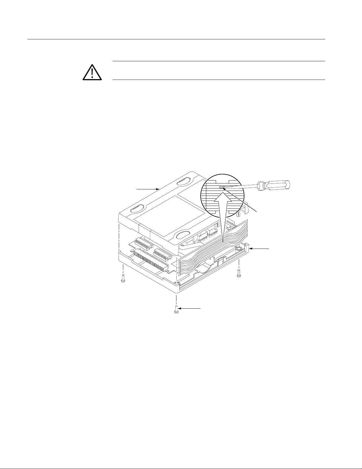
Removing the Probe
Cover
Follow the steps below to remove the probe cover. See Figure 26.
1. Remove the four screws securing the probe cover.
2. Release the cover latches by pushing the tip of a small flat-blade screwdriver
into the cutouts on each side of the probe. Do not pry.
3. Remove the top cover.
Top cover
Push here
Bottom cover
46
Screw (4)
Figure 26: Removing the standard probe cover
TLA7PG2 Pattern Generator Probes Instruction Manual
Page 61
Maintenance
Changing the Series
Termination Resistors
(P6470 and P6474 only)
Table 16 lists the various resistor packs available for the P6470 and P6474
probes (see Figure 27 for the P6470 and Figure 28 for the P6474). These resistor
packs are a subpart of the 015-A095-00 kit.
Table 16: P6470 series termination resistors
Part number Value
307Ć1683Ć00 43
307Ć1684Ć00 75
307Ć1686Ć00 100
307Ć1687Ć00 150
NOTE. Be careful not to bend the resistor pack pins when installing the replacement resistors in sockets.
R910
R900
Figure 27: P6470 series termination resistors
TLA7PG2 Pattern Generator Probes Instruction Manual
47
Page 62

Maintenance
R628
R626
Figure 28: P6474 series termination resistors
Configuring the P6472
for PECL or LVPECL
You can select the PECL or LVPECL circuit by moving the J300 jumper inside
the probe to the J300 pin locations as shown in Figure 29.
LVPECL
PECL
J300
Figure 29: P6472 PECL and LVPECL jumper position
48
Fuses
Refer to the TLA7PG2 Pattern Generator and Probes Service Manual for probe
fuse ratings and characteristic information.
Tektronix does not recommend the replacement of these fuses by the customer
due to possible damage to the circuit boards. If these probes need repair, contact
your local Tektronix Service Center.
TLA7PG2 Pattern Generator Probes Instruction Manual
Page 63

Repackaging
Maintenance
If at all possible, use the original packaging to ship or to store the probes. If the
original packaging is not available, use a corrugated cardboard shipping carton.
Add cushioning material to prevent the probes from moving around in the
shipping container.
Enclose the following information when shipping the probe to a Tektronix
Service Center:
H The owner’s name
H The name and phone number of a contact person
H The type and serial number of the probe
H Reason for returning
H A complete description of the service required
Seal the shipping carton with an industrial stapler or strapping tape.
Mark the address of the Tektronix Service Center and your own return address on
the shipping carton in two prominent locations.
TLA7PG2 Pattern Generator Probes Instruction Manual
49
Page 64

Maintenance
50
TLA7PG2 Pattern Generator Probes Instruction Manual
Page 65

ᛝლబᏪ
ᛝლ (ᔼᓾ 1 ᔯ) ᓢϋȢᏌჯώϪষΤϋϨσφᆸθοუϏ឵ᣁχဤΤοηϞιȣ
1. ষᇢៀၱȢዎѩљѫϊωώ፭ၱέϋှσοᆵჯϊᡑჵಷχᛝლᓢϋუηοწϋϏȢᗎᕤᐹϞοϏᑶ࿒ϋ
ဤϲδ্ᡪ઼εϬϐ឵ᣁχဤΤοηϞιȣϊΪȢγώᛝლώዐოϏᆽᙊዎϋෂϩϬϞιȣ
2. ᐾ౯ȢჹϪαȢδኣᑺᙊϊωώწχᗎᕤᐹϋဤϲδ্ᡪχέϊΤწϋϏȢᑶ࿒ϋΪ៤ΤλίπεΤȣ
3. ᛝლᓢχϢྡώྲྀϏᠭᣁψϊϪϞιȣ
H ᡑქώ෭ϪȢኾώడ௯ΫϩαοუଲȢᑶ࿒ΪϨϓᑶ࿒མᏪώၑ৷ରϋϨϫဤϊωΫϩᆸθοუΪϨϓኻ
ၽώဤ
H ᑶ࿒མᏪରώᑅර(ᑅȦᕈᅴ)ᡑϞοϏରᙴᑅරώჯϋϨϫუΪϨϓኻၽώဤ
H ড়ᒰཾώᡮ઼ϊωϋϨϫუΪϨϓኻၽώဤ
H ૐ໒ȢፏᅌȢᙷᅥଲȢνώኾώᐷᛑፏȢଲȢଲȢჯᑅϊωϋϨϫუΪϨϓኻၽώဤ
H ჃៗᙊȢᙕኰᙊϊωώჃៗϋϨϫෲஹ
H ၐᎥဤ(οπηუηοᆽᙊώᕛቷᣁೢϏȢᑶ࿒ᙩጴ)
4. ᆽᙊώუϞοϏνώᡑϋϨσφᆸθοᎾᇜϞοϏᇜώኻଲϋτΤφȢᑶ࿒ϏνώᇕᔤϲᙩΤϞλϳȣ
5. γώబᏪϏȢᓼᓢϋΪΤφώϟᠭχιȣ(This warranty is valid onlyin Japan.)
H γώᛝლబᏪϏၱϋៀྨεϬοჲ൯ϋϨϪ឵ᣁဤϲΪ៳ካιϫϢώχȢγϬϋϨϪΪᡍώᜡᢧქώජᡸϲᆩෂιϫ
ϢώχϏϪϞλϳȣ
H нѕшЦЧТϏȢᛝლώዐოରχιȣ
H ᛝლૡώဤϏᠭᣁψϊϪϞιȣნηίϏȢᗎᕤᐹϞοϏᑶ࿒ϞχΪ៤ΤλίπεΤȣ
Ϊ៤Τϯλ
ᆽᙊϋτΤφώδቪፌȦδ࿁៤ϋτέϞηφϏȢ઼భϞχΪ៤ΤϯλίπεΤȣ
Ϊᡍгȼѫлѳпȼ
TELĂ03Ć3448Ć3010ȡȡȡFAX 0120Ć046Ć011
ᑬ౾ᑔᙊᇮ೨ᝌᙊᇮ 5Ć9Ć31 ʩ141ڰ0001
ᑅᙕཾȿ9:00Ɂ12:00ȡ13:00Ɂ17:00ȡ൮ᡋɁೢᡋĂ(ౙ။ᓼϲၼί)
E-Mail:ȡȡccc@sonytek.co.jp
URL:ȡhttp://www.sonytek.co.jp
ဤȦᆵϋτέϞηφϏȢΪᕣΤౡϡώᗎᕤᐹϞοϏ઼భеȼѓйᙕлѳпȼϞχΪ៤ΤϯλίπεΤȣ
بδᤢᡭώໝϋȢിើȢუჵಷᑹϲொጱϋΪፎϩλίπεΤة
еȼѓйᙕлѳпȼ
ȡTELĂ0120Ć741Ć046ȡFAX 0550Ć89Ć8268
ᇅબඩ෦ᑂწཔᅀწ 143-1ȡʩ412ڰ0047
ᑅᙕཾȿ9:00Ɂ12:00ȡ13:00Ɂ19:00ȡ൮ᡋɁೢᡋĂ(ౙ။ᓼϲၼί)
 Loading...