

Page 1

Instruction Manual
P6450
Logic Analyzer Probe
with D-MaxtProbing Technology
071-2478-00
There are no current European directives that apply to this product. This product provides cable
and test lead connections to a test object of electronic measuring and test equipment.
Warning
The servicing instructions are for use by qualified
personnel only. To avoid personal injury, do not
perform any servicing unless you are qualified to
do so. Refer to all safety summaries prior to
performing service.
www.tektronix.com
Page 2

Copyright © Tektronix. All rights reserved. Licensed software products are owned by Tektronix or its subsidiaries or
suppliers, and are protected by national copyright laws and international treaty provisions.
Tektronix products are covered by U.S. and foreign patents, issued and pending. Information in this publication supercedes
that in all previously published material. Specifications and price change privileges reserved.
TEKTRONIX and TEK are registered trademarks of Tektronix, Inc.
cLGA is a registered trademark of Amphenol Intercon Systems, Inc.
Velcro is a registered trademark of Velcro Industrie s B.V.
Contacting Tektronix
Tektronix, Inc.
14200 SW Karl Braun Drive
P.O. Box 500
Beaverton, OR 97077
USA
For product information, sales, service, and technical support:
H In North America, call 1-800-833-9200.
H Worldwide, visit www.tektronix.com to find contacts in your are a.
Page 3

Warranty 2
Tektronix warrants that this product will be free from defects in materials and workmanship for a period of one (1)
year from the date of shipment. If any such product proves defective during this warranty peri od, Tektronix, at its
option, either will repair the defective product without charge for parts and labor, or will provide a replacement in
exchange for the defective product. Parts, modules and replacement products used by Tektronix for warranty work
may be new or reconditioned to like new performance. All replaced parts, modules and products become the
property of Tektronix.
In order to obtain service under this warranty, Customer must notify Tektronix of the defect before the expiration
of the warranty period and make suitable arrangements for the performance of service. Customer shall be
responsible for packaging and shipping the defective product to the service center designated by Tektronix, with
shipping charges prepaid. Tektronix shall pay for the return of the product to Customer if the shipment is to a
location within the country in which the Tektronix service center is located. Customer shall be responsible for
paying all shipping charges, duties, taxes, and any other charges for products ret urned to any other locations.
This warranty shall not apply to any defect, failure or damage caused by improper use or improper or inadequate
maintenance and care. Tektronix shall not be obligated to furnish service under this warranty a) to repair damage
resulting from attempts by personnel other than Tektronix representatives to install, repair or service the product;
b) to repair damage resulting from improper use or connection to incompatible equipment; c) to repair any
damage or malfunction caused by the use of non-Tektronix supplies; or d) to service a product that has been
modified or integrated with other products when the effect of such modification or integration increases the time
or difficulty of servicing the product.
THIS WARRANTY IS GIVEN BY TEKTRONIX WITH RESPECT TO THE PRODUCT IN LIEU OF ANY
OTHER WARRANTIES, EXPRESS OR IMPLIED. TEKTRONIX AND ITS VENDORS DISCLAIM ANY
IMPLIED WARRANTIES OF MERCHANTABILITY OR FITNESS FOR A PARTICULAR PURPOSE.
TEKTRONIX’ RESPONSIBILITY TO REP AIR OR REPLACE DEFECTIVE PRODUCTS IS THE SOLE AND
EXCLUSIVE REMEDY PROVIDED TO THE CUSTOMER FOR BREACH OF THIS WARRANTY.
TEKTRONIX AND ITS VENDORS WILL NOT BE LIABLE FOR ANY INDIRECT, SPECIAL, INCIDENTAL,
OR CONSEQUENTIAL DAMAGES IRRESPECTIVE OF WHETHER TEKTRONIX OR THE VENDOR HAS
ADVANCE NOTICE OF THE POSSIBILITY OF SUCH DAMAGES.
Page 4

Page 5

Table of Contents
Preface xi...................................................
Related Documentation xi...........................................
Commonly Used Terms xii...........................................
Operating Basics 1..........................................
Product Description 1..............................................
Attaching Probe Labels 3...........................................
Connecting the Probes to the Logic Analyzer 5..........................
Connecting the Probes to the Target System 6...........................
Using the Probe Retention Assembly 6.............................
Dressing the Probe Cables 11.........................................
Storing the Probe Head 12............................................
Reference 13.................................................
Designing an Interface Between the Probes and a Target System 13...........
Signal Fixturing Considerations 13.................................
Board Design 17...................................................
Probe Dimensions 17............................................
Probe Retention Assembly Dimensions and Keepout 18................
Side-by-side and End-to-end Layout Dimensions 19...................
Signal Routing 20...............................................
Mechanical Considerations 20.....................................
Electrical Considerations 21......................................
Probe Footprint Dimensions 22........................................
Other Design Considerations 23.......................................
Via-in-pa d 23..................................................
Probe Pinout Definition and Channel Assignment 24......................
P6450 Single-ended Probe with D-Max probing technology 24...........
Specifications 27.............................................
Mechanical and Electrical Specifications 27.............................
Maintenance 29..............................................
Probe Calibration 29................................................
Functional Check 29................................................
Inspection and Cleaning 29...........................................
Service Strategy 29.................................................
Legacy Probe and Attachment Support 31...............................
Repackaging Instructions 31..........................................
Replaceable Parts 33..........................................
Parts Ordering Information 33.........................................
Using the Replaceable Parts List 33....................................
Mfr. Code to Manufacturer Cross Index 34...........................
Index 37....................................................
P6450 High-Density Logic Analyzer Probe Instruction Manual
i
Page 6

Table of Contents
List of Tables
Table 1: Probe section and label combinations 3.................
Table 2: Logic analyzer clock and qualifier availability 13..........
T able 3: 2X Demultiplexing source-to-destination
channel assignments 15....................................
Table 4: Channel assignment for a P6450 single-ended
logic analyzer probe 25....................................
T able 5: Mechanical and electrical specifications 27...............
Table 6: Environmental specifications 28........................
ii
P6450 High-Density Logic Analyzer Probe Instruction Manual
Page 7

List of Figures
Table of Contents
Figure i: Flying Lead Set xii....................................
Figure ii: Probe example xiii....................................
Figure 1: P6450 High-Density probe with
D-Max probing technology 1...............................
Figure 2: Attaching labels to the P6450 probe 4..................
Figure 3: Connecting the logic analyzer probe 5..................
Figure 4: Installing the probe retention assembly 7...............
Figure 5: Proper handling of the interface clip 8..................
Figure 6: Connecting the probes to the target system 9............
Figure 7: Proper dressing of the probe cables 11...................
Figure 8: Protecting the probe head 12...........................
Figure 9: P6450 probe dimensions 17............................
Figure 10: Alternate retention assembly dimensions 18.............
Figure 11: Keepout area 18....................................
Figure 12: Side-by-side layout 19...............................
Figure 13: End-to-end layout 19................................
Figure 14: Signal routing on the target system 20..................
Figure 15: High-Density probe load model 21.....................
Figure 16: Probe footprint dimensions on the PCB 22..............
Figure 17: Optional Via-in-Pad placement recommendation 23......
Figure 18: P6450 single-ended PCB footprint pinout detail 24.......
Figure 19: Replacing the cLGA clip 30..........................
Figure 20: P6450 High-Density probe accessories 35...............
Figure 21: Optional accessories 36..............................
P6450 High-Density Logic Analyzer Probe Instruction Manual
iii
Page 8

Table of Contents
iv
P6450 High-Density Logic Analyzer Probe Instruction Manual
Page 9

General Safety Summary
Review the following safety precautions to avoid injury and prevent damage to
this product or any products connected to it.
To avoid potential hazards, use this product only as specified.
Only qualified personnel should perform service procedures.
While using this product, you may need to access other parts of the system. Read
the General Safety Summary in other system manuals for warnings and cautions
related to operating the system.
ToAvoidFireor
Personal Injury
Connect and Disconnect Properly. Connect the probe output to the measurement
instrument before connecting the probe to the circuit under test. Disconnect the
probe input and the probe ground from the circuit under test before disconnecting
the probe from the measurement instrument.
Ground the Product. This product is indirectly grounded through the grounding
conductor of the mainframe power cord. To avoid electric shock, the grounding
conductor must be connected to earth ground. Before making connections to the
input or output terminals of the product, ensure that the product is properly
grounded.
Observe All Terminal Ratings. To avoid fire or shock hazard, observe all ratings
and markings on the product. Consult the product manual for further ratings
information before making connections to the product.
The inputs are not rated for connection to mains or Category II, III, or IV
circuits.
Do not apply a potential to any terminal, including the common terminal, that
exceeds the maximum rating of that terminal.
Power Disconnect. The power cord disconnects the product from the power
source. Do not block the power cord; it must remain accessible to the user at all
times.
Do Not Operate Without Covers. Do not operate this product with covers or panels
removed.
Do Not Operate With Suspected Failures. If you suspect there is damage to this
product, have it inspected by qualified service personnel.
Avoid Exposed Circuitry. Do not touch exposed connections and components
when power is present.
Do Not Operate in Wet/Damp Conditions.
Do Not Operate in an Explosive Atmosphere.
P6450 High-Density Logic Analyzer Probe Instruction Manual
v
Page 10
General Safety Summary
Keep Product Surfaces Clean and Dry.
Provide Proper Ventilation. Refer to the manual’s instructions for details on
installing the product so it has proper ventilation.
Symbols and Terms
Terms in this Manual. These terms may appear in this manual:
WARNING. Warning statements identify conditions or practices that could result
in injury or loss of life.
CAUTION. Caution statements identify conditions or practices that could result in
damage to this product or other property.
Terms on the Product. These terms may appear on the product:
DANGER indicates an injury hazard immediately accessible as you read the
marking.
WARNING indicates an injury hazard not immediately accessible as you read the
marking.
CAUTION indicates a hazard to property including the product.
Symbols on the Product. The following symbol may appear on the product:
CAUTION
Refer to Manual
vi
Earth Terminal
Chassis Ground
P6450 High-Density Logic Analyzer Probe Instruction Manual
Page 11

Service Safety Summary
Only qualified personnel should perform service procedures. Read this Service
Safety Summary and the General Safety Summary before performing any service
procedures.
Do Not Service Alone. Do not perform internal service or adjustments of this
product unless another person capable of rendering first aid and resuscitation is
present.
Disconnect Power. To avoid electric shock, switch off the instrument power, then
disconnect the power cord from the mains power.
Use Care When Servicing With Power On. Dangerous voltages or currents may
exist in this product. Disconnect power, remove battery (if applicable), and
disconnect test leads before removing protective panels, soldering, or replacing
components.
To avoid electric shock, do not touch exposed connections.
P6450 High-Density Logic Analyzer Probe Instruction Manual
vii
Page 12

Service Safety Summary
viii
P6450 High-Density Logic Analyzer Probe Instruction Manual
Page 13

Environmental Considerations
This section provides information about the environmental impact of the
product.
Product End-of-Life
Handling
Restriction of Hazardous
Substances
Observe the following guidelines when recycling an instrument or component:
Equipment Recycling. Production of this equipment required the extraction and
use of natural resources. The equipment may contain substances that could be
harmful to the environment or human health if improperly handled at the
product’s end of life. In order to avoid release of such substances into the
environment and to reduce the use of natural resources, we encourage you to
recycle this product in an appropriate system that will ensure that most of the
materials are reused or recycled appropriately.
The symbol shown to the left indicates that this product
complies with the European Union’s requirements
according to Directive 2002/96/EC on waste electrical and
electronic equipment (WEEE). For information about
recycling options, check the Support/Service section of the
Tektronix Web site (www.tektronix.com).
This product has been classified as Monitoring and Control equipment, and is
outside the scope of the 2002/95/EC RoHS Directive. This product is known to
contain lead and hexavalent chromium.
P6450 High-Density Logic Analyzer Probe Instruction Manual
ix
Page 14

Environmental Considerations
x
P6450 High-Density Logic Analyzer Probe Instruction Manual
Page 15

Preface
This document provides information on using and servicing the P6450 logic
analyzer probe.
Related Documentation
The following table lists related documentation that is available for your
instrument. The documentation is available on the TLA Documentation CD and
on the Tektronix Web site (www.Tektronix.com/manuals).
For documentation not specified in the table, contact your local Tektronix
representative.
Table i: Product documentation
Item Purpose Location
TLA Quick Start User Manual High-level operational overview
Online Help In depth operation and UI help
Installation Quick Reference Cards High-level installation information
Installation Manuals Detailed first-time installation infor-
mation
XYZs of Logic Analyzers Introduction to logic analyzer basics
Product Specifications TLA product specification documents
TPI.NET Documentation Detailed information for controlling
the logic analyzer using .NET
Field upgrade kits Upgrade information for your logic
analyzer product
Optional Service Manuals Self-service documentation for
modules and mainframes
+ +
P6450 High-Density Logic Analyzer Probe Instruction Manual
xi
Page 16
Preface
Commonly Used Terms
Refer to the following list of commonly used terms throughout the manual.
cLGA
Compression Footprint
D-Max probing technology
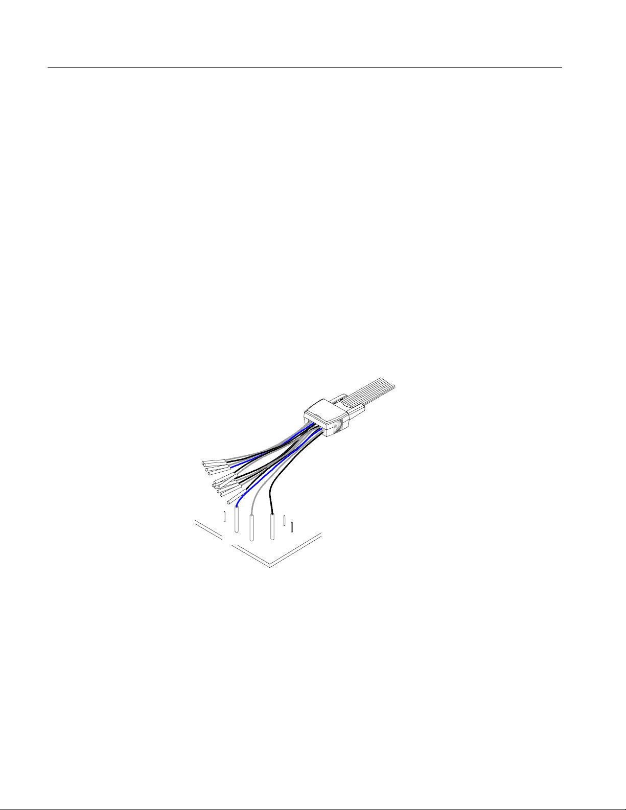
Flying Lead Set
An acronym for compression Land Grid Array, a connector that provides an
electrical connection between a PCB and the probe input circuitry.
A connectorless, solderless contact between your PCB and the P6450 probes.
Connection is obtained by applying pressure between your PCB and the probe
through a cLGA c-spring.
Trademark name that describes the technology used in the P6450 high-density
logic analyzer probe.
A lead set designed to attach to a P6450 probe to provide general-purpose
probing capability. See Figure i.
xii
Functional Check
Procedure
Keepout Area
CLK
Figure i: Flying Lead Set
Functional check procedures verify the basic functionality of the probes by
confirming that the probes recognize signal activity at the probe tips.
An area on a printed circuit board in which component, trace, and/or via
placement may be restricted.
GND
SIG
P6450 High-Density Logic Analyzer Probe Instruction Manual
Page 17
Preface
Module
Module End
PCB
Probe
The unit that plugs into a mainframe that provides instrument capabilities such
as logic analysis.
The end of the probe that plugs into the module unit.
An acronym for Printed Circuit Board; also known as Etched Circuit Board
(ECB).
The device that connects a module with a target system. See F igure ii.
Module end
Probe Head
SUT
Probe head
P6450 Single-ended
probe
Figure ii: Probe example
The end of the probe that connects to the target system or probe adapter.
An acronym for System Under Test; also referred to as target system.
P6450 High-Density Logic Analyzer Probe Instruction Manual
xiii
Page 18

Preface
xiv
P6450 High-Density Logic Analyzer Probe Instruction Manual
Page 19

Operating Basics
Product Description
This section provides a brief description of the Tektronix P6450 High-Density
Logic Analyzer Probe, information on attaching color-coded probe labels, and
probe and adapter connection instructions from the logic analyzer to the target
system.
The P6450 probe is a 34-channel, high-density connectorless probe with D-Max
probing technology (see Figure 1). The probe consists of one probe head that has
34 channels (32 data and 2 clock/qual).
Figure 1: P6450 High-Density probe with D-Max probing technology
The following list details the capabilities and qualities of the P6450 probe:
H Single-ended data inputs
H cLGA contact eliminates need for built-in connector
H Footprint supports direct signal pass-through
H Supports PCB thickness of 1.27 mm to 6.35 mm (0.050 in to 0.250 in)
P6450 High-Density Logic Analyzer Probe Instruction Manual
1
Page 20

Operating Basics
H Consists of one independent probe head of 34 channels (32 data and
2 clock/quals), and two 34-channel module end connectors.
H Narrow 34-channel probe head makes for easier placement and layout
H 2X mode, (for example, 1:2 demultiplexing) uses one-half of the probe head
H Color-coded keyed attachment
H --3.5 V to +6.5 V input operating range
H 500 mV minimum single-ended signal amplitude
H Minimal loading of 0.7 pF at 20 kΩ to ground
H Operation in normal or inverted polarity is acceptable (clock only)
NOTE. Refer to Figure 14 on page 20 for P6450 probe routing and pinout
information.
2
P6450 High-Density Logic Analyzer Probe Instruction Manual
Page 21

Operating Basics
Attaching Probe Labels
When you purchase the P6450 logic analyzer probe, you must apply the
color-coded labels as described in this section. The labels help you identify the
probe connections at the logic analyzer end and at the target system end.
Table 1 lists the probe section and label color combinations. Refer to Table 1 and
to Figure 2 when you attach the probe labels.
Table 1: Probe section and label combinations
Probe section Channels Label color Probe section Channels Label color
A3-A2 CK0, A3:7--0, A2:7-0 Brown A1-A0 CK1, A1:7-0, A0:7-0 Orange
D3-D2 QUAL0, D3:7-0, D2:7-0 Blue D1-D0 CK2, D1:7-0, D0:7-0 Yellow
C3-C2 CK3, C3:7-0, C2:7-0 White C1-C0 QUAL1, C1:7-0, C0:7-0 Gray
E3-E2 QUAL3, E3:7-0, E2:7-0 Green E1-E0 QUAL2, E1:7-0, E0:7-0 Violet
P6450 Labels
Use the following instructions to attach probe labels to your Tektronix P6450
Logic Analyzer Probe.
NOTE. Always use flat-nosed tweezers to remove the labels from the sheet of
labels. Never peel labels with your fingers. The labels are made of soft vinyl and
can stretch and distort easily. To avoid stretching the label, always grasp it from
the top right corner while removing it from the sheet of labels.
The adhesive on the vinyl labels is extremely strong. Carefully align each label
to the intended outline on the module end and probe head before attaching it to
the probe. Once labels are placed on the probe, they become very difficult to
remove.
You will be attaching labels to the logic analyzer end and both sides of the probe
head. Refer to Figure 2 and use the following steps to attach the probe labels:
1. Identify the module end of the probe cable.
2. From the sheet of labels, locate the color-coded label for the logic analyzer
end of the probe cable.
3. Attach the matching colored labels to the probe head on the other end of the
probe cable.
P6450 High-Density Logic Analyzer Probe Instruction Manual
3
Page 22

Operating Basics
P6450 Singl e--ended
SLOT
Q0
A3D3 A2D2
P6450
A3
CK0
SLOT
A2
P6450 Single--ended
SLOT
CK0
A3A2 D3 D2
Figure 2: Attaching labels to the P6450 probe
4
D3
Q0
P6450
SLOT
D2
P6450 High-Density Logic Analyzer Probe Instruction Manual
Page 23

Connecting the Probes to the Logic Analyzer
Connect the logic analyzer probe and the optional retaining brackets as shown in
Figure 3. The retaining brackets and hardware ship with the logic analyzer.
Match
color-coded labels
Operating Basics
P6450
Attach optional
probe retainer
brackets
Figure 3: Connecting the logic analyzer probe
NOTE. The probe can be connected to the logic analyzer when it is powered on.
P6450 High-Density Logic Analyzer Probe Instruction Manual
5
Page 24

Operating Basics
Connecting the Probes to the Target System
You can connect the P6450 probe to the target system without turning off the
power to the target system. The target system must have the probe retention
assembly installed. Installation procedures are described on the following pages.
Cleaning the
Compression Footprints
Using the Probe Retention
Assembly
The following procedure is recommended to obtain best performance.
CAUTION. To avoid electrical damage, always power off your target system
before cleaning the compression footprint.
Prior to connecting the probe to the target system, the compression footprints on
the board should be properly cleaned, according to the following steps:
1. Use a lint-free, clean-room cloth lightly moistened with electronic/reagent
grade isopropyl alcohol, and gently wipe the footprint surface.
2. Remove any remaining lint using a nitrogen air gun or clean, oil-free dry air.
The probe retention assembly provides a housing around the connector footprint
to help stabilize the probe. To install the probe retention assembly on the circuit
board, refer to Figure 4 on page 7 and do the following:
1. Locate the correct footprint. If you intend to use multiple probes, your PCB
has multiple footprints. Be careful to select the correct one.
2. Clean the compression footprint as described above.
3. Align the retention assembly over the footprint so that the keying pin on the
retention assembly lines up with the keying pin hole on the footprint.
4. Insert the retention assembly into the holes in the footprint on the PCB.
NOTE. The following two steps are important to ensure that the retention
assembly is correctly mounted and that the probe makes proper contact with the
PCB.
5. Hold the retention assembly so that it is firmly flush with the surface of the
footprint, and the four anchoring posts extend through the circuit board to
the opposite side.
6. Using a pair of needle--nose pliers, grasp one of the posts. Using the circuit
board hole as a fulcrum, bend the post outward so that it is flush with the
PCB surface, anchoring the assembly to the PCB. Bend the other three posts
in the same manner.
7. Solder the anchoring posts to the PCB.
6
P6450 High-Density Logic Analyzer Probe Instruction Manual
Page 25

Operating Basics
Retention
assembly
Keying
pin hole
PCB
~0
45
Figure 4: Installing the probe retention assembly
Press down
on retention
assembly
PCB
90
Solder
P6450 High-Density Logic Analyzer Probe Instruction Manual
7
Page 26

Operating Basics
Handling the cLGA
Interface Clip
(Probe Head)
The cLGA interface clip in the probe head should always be handled with care.
Keep the following points in mind when you handle the clip:
H Always handle the cLGA interface clip by the outer edges, and be careful to
avoid the contacts in the center. Do not touch the contacts with your fingers,
tools, wipes, or any other devices. See Figure 5.
Figure 5: Proper handling of the interface clip
H Do not expose the connector to liquids or dry chemicals.
H If the board pad array needs to be cleaned, only use isopropyl alcohol and
lint-free cloth as described above.
H Immediately following cleaning, or immediately prior to placement of
connector to circuit board, blow off the board pad array and connector
contact array with clean, oil-free dry air or nitrogen to remove loose debris.
First start the blowing process by aiming away from the array areas, and then
sweep across the pad and contact arrays in a repeated motion to remove
loose debris.
H Place the connector onto the board pad array using the bosses or locator pins
for alignment. Use care to prevent incidental contact with other surfaces or
edges in the connector contact array area prior to board placement.
H Always store the probe head in the protective cover when not in use.
See Figure 8 on page 12.
8
P6450 High-Density Logic Analyzer Probe Instruction Manual
Page 27

Operating Basics
Connect the Probe
Refer to Figure 6, and connect the probes using the following steps.
1. Align the silver screw on the probe to the silver side of the retention
assembly.
Black
Silver
Retention assembly
Note: The retention assembly is visually keyed
(one side is black and one side is silver).
Figure 6: Connecting the probes to the target system
2. Start both screws in the retention assembly, and tighten them evenly to
ensure that the probe approaches and mates squarely to the PCB. If access is
limited, use the adjustment tool that came with your probe. The probe is
completely fastened to the PCB when the screws stop in the assembly.
3. Verify that all of the channels are functional. If any channels appear to be
nonfunctional, see Troubleshooting Probe Connections to the SUT on
page 10.
P6450 High-Density Logic Analyzer Probe Instruction Manual
9
Page 28

Operating Basics
Troubleshooting Probe
Connections to the SUT
The most obvious symptom of a problem with the probe installation is seeing
incorrect data in the logic analyzer acquisition. However, the nature of the
incorrect data has a very consistent characteristic; the data from multiple
channels go to a logic low and stay there. Intermittent bad data, or a single dead
channel are not failures typically associated with probe installation problems.
1. Slightly move the probe head to either side, or press down on the probe head
while making new acquisitions. If good data is now being acquired, then the
probe mounting is most likely the cause.
2. If good data is not acquired, then remove the probe and check the retention
assembly for too much play. If there is significant play, then the probe
mounting is most likely the cause.
3. If the retention assembly has minimal play and you cannot see a gap between
the bottom of the assembly and the circuit board surface, then move the
probe with bad data from one logic analyzer probe location to another.
4. If the problem follows the probe, then the probe is the problem. Visually
inspect the cLGA interface clip on the probe for any damage or missing
c-spring metal contacts.
If there is damage to the interface clip, or if any c-spring metal contacts are
missing, replace the cLGA interface clip. (See Replacing the cLGA Clip on
page 30 and Replaceable Parts, beginning on page 33 for more information.)
5. If the problem doesn’t follow the probe, it is either the logic analyzer or the
probe connection at its previous location. Move the probe back to the
original location to be certain it was not a connection problem at the logic
analyzer end.
6. Place another probe in the retention assembly of the original probe. If the
new probe acquires data, then the old probe is probably at fault.
10
P6450 High-Density Logic Analyzer Probe Instruction Manual
Page 29

Dressing the Probe Cables
Use the Velcro cable managers to combine the cables together or to help relieve
strain on the probe connections.
Hang the probe cables so that you relieve the tension on the probes at the
retention posts. See Figure 7.
Operating Basics
Probe cables
PCB
Bad contact
Good
Cable hanger
Logic Analyzer
Bad
Figure 7: Proper dressing of the probe cables
P6450 High-Density Logic Analyzer Probe Instruction Manual
11
Page 30

Operating Basics
Storing the Probe Head
To protect the interface clip, it is important to properly store the probe head when
the probe is not in use. See Figure 8.
Gently slide the probe cover over the probe end and store the probe.
Protective
cover
Figure 8: Protecting the probe head
12
P6450 High-Density Logic Analyzer Probe Instruction Manual
Page 31

Reference
TLA
This section provides reference information for the P6450 High-Density Probe
with D-Max probing technology.
Designing an Interface Between the Probes and a Target System
Once you have determined which probe is required, use the following information to design the appropriate connector into your target system board.
Signal Fixturing
This section contains information to consider for signal fixturing.
Considerations
Clocks and Qualifiers. Every logic analyzer has some special purpose input
channels. Inputs designated as clocks can cause the logic analyzer to store data.
Qualifier channels can be logically ANDed and ORed with clocks to further
define when the logic analyzer should latch data from the system under test.
Routing the appropriate signals from your design to these inputs ensures that the
logic analyzer can acquire data correctly. Unused clocks can be used as qualifier
signals.
Depending on the channel width, each TLA5000B Series logic analyzer will
have a different set of clock and qualifier channels. Table 2 shows the clock and
qualifier channels available for each module.
Table 2: Logic analyzer clock and qualifier availability
Clock Inputs Qualifier Inputs
Module
TLA5201B n n
TLA5202B n n n n
TLA5203B n n n n n n
TLA5204B n n n n n n n n
CLK:0
CLK:1 CLK:2 CLK:3 QUAL:0 QUAL:1 QUAL:2 QUAL:3
All clock and qualifier channels are stored. The logic analyzer always stores the
logic state of these channels every time it latches data.
Since clock and qualifier channels are stored in the logic analyzer memory, there
is no need to double probe these signals for timing analysis. When switching
from state to timing analysis, all of the clock and qualifier signals will be visible.
P6450 High-Density Logic Analyzer Probe Instruction Manual
13
Page 32

Reference
This allows you to route signals not needed for clocking to the unused clock and
qualifier channels.
It is a good practice to take advantage of the unused clock and qualifier channels
to increase your options for when you will latch data. Routing several clocks and
strobes in your design to the logic analyzer clock inputs will provide you with a
greater flexibility in the logic analyzer Setup menu.
As an example, look at a microprocessor with a master clock, data strobe, and an
address strobe. Routing all three of these signals to logic analyzer clock inputs
will enable you to latch data on the processor master clock, only when data is
strobed, or only when address is strobed. Some forethought in signal routing can
greatly expand the ways in which you can latch and analyze data.
A microprocessor also provides a good example of signals that can be useful as
qualifiers. There are often signals that indicate data reads versus data writes
(R/W), signals that show when alternate bus masters have control of the
processor buses (DMA), and signals that show when various memory devices are
being used (ChipSel). All of these signals are good candidates for assignment to
qualifier channels.
By logically ANDing the clock with one of these qualifiers you can program the
logic analyzer to store only data reads or data writes. Using the DMA signal as a
qualifier provides a means of filtering out alternate bus master cycles. Chip
selects can limit data latching to specific memory banks, I/O ports, or peripheral
devices.
14
P6450 High-Density Logic Analyzer Probe Instruction Manual
Page 33

Demultiplexing Multiplexed Buses. TLA5000B Series logic analyzers support 2X
demultiplexing. Each signal on a dual multiplexed bus can be demultiplexed into
its own logic analyzer channel. See Table 3 to determine the correct channel
groups to use.
Table 3: 2X Demultiplexing source-to-destination channel assignments
Reference
Source
connecting channel
groups
A3:7--0 D3:7--0 D3:7--0 C3:7--0 C3:7--0
A2:7--0 D2:7--0 D2:7--0 C2:7 --0 C2:7--0
A1:7--0 D1:7--0 D1:7--0 D1:7 --0
A0:7--0 D0:7--0 D0:7--0 D0:7 --0
C3:7--0 C1:7--0 C1:7 --0
C2:7--0 C0:7--0 C0:7 --0
E3:7--0 E1:7--0
E2:7--0 E0:7--0
CLK:0 QUAL:1 QUAL:1
CLK:1 QUAL:0 QUAL:0
CLK:2 QUAL:3
CLK:3 QUAL:2
Destination channels receiving target system test data
TLA5204B TLA5203B TLA5202B TLA5201B
When demultiplexing data there is no need to connect the destination channels to
the multiplexed bus. Data from the source channels are routed to the destination
channels internal to the logic analyzer. Table 3 shows the mapping of source
channels to destination channels.
Demultiplexing affects only the main memory for the destination channels. This
means that the MagniVu memory is filled with data from whatever is connected
to the demultiplexing destination channel probe inputs. This provides an
opportunity to acquire high resolution MagniVu data on a few extra channels.
Connecting the demultiplexing destination channels to other signals will allow
viewing of their activity in the MagniVu memory but not the main memory.
P6450 High-Density Logic Analyzer Probe Instruction Manual
15
Page 34

Reference
High Resolution Timing. The high resolution timing mode provides double the
normal 500 MHz sample rate on one-half of the channels. By trading half of the
analyzer’s channels, the remaining channels can be sampled at a 1 GHz rate with
double the memory depth.
By taking care to assign critical signals to the demultiplexing source channels,
you can obtain extra timing resolution where it is most needed. Since
demultiplexing affects only the main memory you will still have the MagniVu
data available for all of the signals that are disconnected from the main memory
when you switch to the high resolution timing modes.
Range Recognition. When using range recognizers, the probe groups and probe
channels must be in hardware order. Probe groups must be used from the
most-significant probe group to the least-significant probe group based on the
following order:
C3 C2 C1 C0 E3 E2 E1 E0 A3 A2 D3 D2 A1 A0 D1 D0 Q3 Q2 Q1 Q0 CK3
CK2 CK1 CK0
Probe channels must be from the most-significant channel to the least-significant
channel based on the following order:
76543210
The above examples assumes a 136-channel logic analyzer. The missing
channels in logic analyzers with fewer than 136 channels are ignored.
16
P6450 High-Density Logic Analyzer Probe Instruction Manual
Page 35

Board Design
Reference
This section provides information that helps you design your PCB mechanically
and electrically for use with the P6450 probe.
Probe Dimensions
32.56 mm
(1.282 in)
P6450
4.60 mm
(0.181 in)
Figure 9 shows the probe dimensions for the P6450 probe.
1828.80 mm
(72.00 in)
P6450 Single--ended
SLOT
CK0
A3A2 D3 D2
69.93 mm
(2.753 in)
D3
Q0
P6450
SLOT
D2
Figure 9: P6450 probe dimensions
P6450 High-Density Logic Analyzer Probe Instruction Manual
17
Page 36

Reference
Probe Retention
Assembly Dimensions
and Keepout
The probe retention assembly provides a housing around the connector footprint
to help stabilize the probe. Figure 10 shows the dimensions of the assembly.
All dimensions are per standard IPC tolerance, which is ±0.004 in.
CAUTION. To avoid solder creep, bend the assembly wires out after you insert the
wires in the board, and then solder the wires.
6.985 mm
(0.275 in)
10.92 mm
(0.430 in)
35.814 mm
(1.410 in)
Retention
wires
Figure 10: Alternate retention assembly dimensions
Figure 11 shows the keep out area required for the alternate retention assembly.
Vias must be placed outside of the keepout area. Any traces routed on the top
layer of the board must stay outside of the keepout area. Traces may be routed on
inner layers of the board through the keepout area.
35.814 mm
(1.410 in)
6.985 mm
(0.275 in)
Keepout
area
27.965 mm
(1.101 in)
4.902 mm
(0.193 in)
Figure 11: Keepout area
18
P6450 High-Density Logic Analyzer Probe Instruction Manual
Page 37

Reference
6.98 mm
(0.275 in)
Side-by-side and
End-to-end Layout
Dimensions
Figure 12 shows the dimensions for side-by-side footprint layout.
35.81 mm
(1.410 in)
13.97 mm
(0.550 in)
Figure 12: Side-by-side layout
Figure 13 shows the dimensions for an end-to-end footprint layout.
35.81 mm
(1.410 in)
35.81 mm
(1.410 in)
Figure 13: End-to-end layout
P6450 High-Density Logic Analyzer Probe Instruction Manual
19
Page 38

Reference
Signal Routing
Figure 14 shows examples of pass-through signal routing for a single-ended data
configuration.
Signal pads
Ground
Single--ended pinout
Figure 14: Signal routing on the target system
Mechanical
Considerations
This section provides information on compression footprint requirements and
physical attachment requirements.
The PCB holes, in general, do not have an impact upon the integrity of your
signals when the signals routed around the holes have the corresponding return
current plane immediately below the signal trace for the entire signal path from
driver to receiver.
NOTE. For optimum signal integrity, there should be a continuous, uninterrupted
ground return plane along the entire signal path.
20
P6450 High-Density Logic Analyzer Probe Instruction Manual
Page 39

Reference
Electrical Considerations
This section provides information on transmission lines and load models for the
P6450 probe.
The low-frequency model is typically adequate for rise and fall times of 1 ns or
slower in a typical 25 Ω source impedance environment (50 Ω runs with a
pass-through connection). For source impedance outside this range, and/or rise
and fall times faster than 1 ns, use the high-frequency model to determine if a
significant difference is obtained in the modeling result.
The compression land pattern pad is not part of the load model. Make sure that
you include the compression land pad in the modeling.
Transmission Lines. Due to the high performance nature of the interconnect,
ensure that stubs, which are greater than 1/4 length of the signal rise time, are
modeled as transmission lines.
P6450 Probe Load Model. The following electrical model (see Figure 15) includes
a low-frequency model of the High-Density Single-Ended Probe.
C1
0.7 pF
R1
20 k Ω
Low frequency probe load
Figure 15: High-Density probe load model
P6450 High-Density Logic Analyzer Probe Instruction Manual
21
Page 40

Reference
Probe Footprint Dimensions
Use the probe footprint dimensions in Figure 16 to lay out your circuit board
pads and holes for attaching the retention posts. If you are using the alternate
retention assembly, all dimensions remain the same as shown below, except the
overall length and width. (Refer to Figure 10 on page 18.) Pad finishes that are
supported include immersion gold, immersion silver, and hot air solder level.
All dimensions are per standard IPC tolerance, which is ±0.004 in.
NOTE. Tektronix recommends using immersion gold surface finish for best
performance.
Tektronix also recommends that the probe attachment holes float or remain
unconnected to a ground plane. This prevents overheating the ground plane and
promotes quicker soldering of the retention posts to your PCB. The probe
retention posts are designed to allow you to solder the retention posts from either
side of your PCB.
0.84 mm
(0.033 in)
Nonplated thru hole
1.72 mm
2.35 mm
(0.0925 in)
4.7 mm
(0.185 in)
1.72 mm
(0.068 in)
(0.068 in)
1.04 mm
(0.041 in)
0.64 mm
(0.025 in)
0.71 mm
(0.028 in)
1mmtypical
(0.03937 in)
0.58 mm
(0.023 in)
2.98 mm
(0.117 in)
Figure 16: Probe footprint dimensions on the PCB
NOTE. You must maintain a solder mask web between the pads when traces are
routed between pads on the same layer. The solder mask must not encroach onto
the pads within the pad dimensions shown in Figure 11 on page 18.
34.04 mm
(1.340 in)
31.95 mm
(1.258 in)
26 mm
(1.024 in)
4x dia. 0.71 mm
(0.028 in)
Plated thru hole
4X dia. 1.22 mm
(0.048 in)
Annular ring
1.27 mm
(0.050 in)
22
P6450 High-Density Logic Analyzer Probe Instruction Manual
Page 41

Other Design Considerations
Reference
Via-in-pad
Traditional layout techniques require vias to be located next to a pad and a signal
routed to the pad, causing a stub and more PCB board area to be used for the
connection. Many new digital designs require you to minimize the electrical
effects of the logic analyzer probing that you design into the circuit board.
Using via-in-pad to route signals to the pads on the circuit board allows you to
minimize the stub length of the signals on your board, thus providing the
smallest intrusion to your signals. It also enables you to minimize the board area
that is used for the probe footprint and maintain the best electrical performance
of your design.
Figure 17 shows a footprint example where two pads use vias. Detail A describes
the recommended position of the via with respect to the pad.
All dimensions are per standard IPC tolerance, which is ±0.004 in.
See detail A
Maxviadia0.25mm
(0.010 in)
Dia0.51mm
(0.020 in)
0.32 mm
(0.013 in)
0.04 mm
(0.002 in)
Detail A
Scale 50.000
Figure 17: Optional Via-in-Pad placement recommendation
P6450 High-Density Logic Analyzer Probe Instruction Manual
23
Page 42

Reference
Probe Pinout Definition and Channel Assignment
This section contains probe pinout definitions and channel assignment tables for
the P6450 probe.
P6450 Single-ended Probe
with D-Max probing
technology
G D2 D3 G D6 D7 G D8 D9 G D12 D13 G D16 D17 G D20 D21 G NC G D26 D27 G D30 D31
B1
A1
Figure 18 shows the pad assignments, pad numbers, and signal names for the
PCB footprint of the P6450 single-ended logic analyzer probe. The P6450 probe
has 32 data channels, one clock, and one qualifier for each footprint.
Figure 18: P6450 single-ended PCB footprint pinout detail
Table 4 on page 25 lists the channel mapping to a logic analyzer module for a
P6450 single-ended logic analyzer probe.
CK2
B27
A27
GD29D28GD25D24GD23D22GD19D18GD15D14GD11D10GNCCK1GD5D4GD1D0
24
P6450 High-Density Logic Analyzer Probe Instruction Manual
Page 43

Reference
Table 4: Channel assignment for a P6450 single-ended logic analyzer probe
136 Channel 68 Channel
102 Channel 34 Channel
Pin number Signal name Probe4 Probe 3 Probe 2 Probe 1 Probe 2 Probe 1
A1 D0 E2:0 A2:0 A0:0 C2:0 A0:0 C2:0
A2 D1 E2:1 A2:1 A0:1 C2:1 A0:1 C2:1
A3 GND GND GND GND GND GND GND
A4 D4 E2:4 A2:4 A0:4 C2:4 A0:4 C2:4
A5 D5 E2:5 A2:5 A0:5 C2:5 A0:5 C2:5
A6 GND GND GND GND GND GND GND
A7 CK1 Q3 CK0 CK1 CK3 CK1 CK3
A8 NC NC NC NC NC NC NC
A9 GND GND GND GND GND GND GND
A10 D10 E3:2 A3:2 A1:2 C3:2 A1:2 C3:2
A11 D11 E3:3 A3:3 A1:3 C3:3 A1:3 C3:3
A12 GND GND GND GND GND GND GND
A13 D14 E3:6 A3:6 A1:6 C3:6 A1:6 C3:6
A14 D15 E3:7 A3:7 A1:7 C3:7 A1:7 C3:7
A15 GND GND GND GND GND GND GND
A16 D18 E1:5 D3:5 D1:5 C1:5 D1:5 A3:5
A17 D19 E1:4 D3:4 D1:4 C1:4 D1:4 A3:4
A18 GND GND GND GND GND GND GND
A19 D22 E1:1 D3:1 D1:1 C1:1 D1:1 A3:1
A20 D23 E1:0 D3:0 D1:0 C1:0 D1:0 A3:0
A21 GND GND GND GND GND GND GND
A22 D24 E0:7 D2:7 D0:7 C0:7 D0:7 A2:7
A23 D25 E0:6 D2:6 D0:6 C0:6 D0:6 A2:6
A24 GND GND GND GND GND GND GND
A25 D28 E0:3 D2:3 D0:3 C0:3 D0:3 A2:3
A26 D29 E0:2 D2:2 D0:2 C0:2 D0:2 A2:2
A27 GND GND GND GND GND GND GND
P6450 High-Density Logic Analyzer Probe Instruction Manual
25
Page 44

Reference
Table 4: Channel assignment for a P6450 single-ended logic analyzer probe (Cont.)
68 Channel136 Channel
34 Channel102 Channel
Pin number Probe 1Probe 2Probe 1Probe 2Probe 3Probe4Signal name
B1 GND GND GND GND GND GND GND
B2 D2 E2:2 A2:2 A0:2 C2:2 A0:2 C2:2
B3 D3 E2:3 A2:3 A0:3 C2:3 A0:3 C2:3
B4 GND GND GND GND GND GND GND
B5 D6 E2:6 A2:6 A0:6 C2:6 A0:6 C2:6
B6 D7 E2:7 A2:7 A0:7 C2:7 A0:7 C2:7
B7 GND GND GND GND GND GND GND
B8 D8 E3:0 A3:0 A1:0 C3:0 A1:0 C3:0
B9 D9 E3:1 A3:1 A1:1 C3:1 A1:1 C3:1
B10 GND GND GND GND GND GND GND
B11 D12 E3:4 A3:4 A1:4 C3:4 A1:4 C3:4
B12 D13 E3:5 A3:5 A1:5 C3:5 A1:5 C3:5
B13 GND GND GND GND GND GND GND
B14 D16 E1:7 D3:7 D1:7 C1:7 D1:7 A3:7
B15 D17 E1:6 D3:6 D1:6 C1:6 D1:6 A3:6
B16 GND GND GND GND GND GND GND
B17 D20 E1:3 D3:3 D1:3 C1:3 D1:3 A3:3
B18 D21 E1:2 D3:2 D1:2 C1:2 D1:2 A3:2
B19 GND GND GND GND GND GND GND
B20 NC NC NC NC NC NC NC
B21 CK2 Q2 Q0 CK2 Q1 CK2 CK0
B22 GND GND GND GND GND GND GND
B23 D26 E0:5 D2:5 D0:5 C0:5 D0:5 A2:5
B24 D27 E0:4 D2:4 D0:4 C0:4 D0:4 A2:4
B25 GND GND GND GND GND GND GND
B26 D30 E0:1 D2:1 D0:1 C0:1 D0:1 A2:1
B27 D31 E0:0 D2:0 D0:0 C0:0 D0:0 A2:0
26
P6450 High-Density Logic Analyzer Probe Instruction Manual
Page 45

Specifications
Mechanical and Electrical Specifications
Table 5 lists the mechanical and electrical specifications for the P6450 probe.
The electrical specifications apply when the probe is connected between a
compatible logic analyzer and a target system.
Refer to the Tektronix TLA5000B Logic Analyzer Product Specifications &
Performance Verification document (available on the Tektronix Logic Analyzer
Family Product Documentation CD or downloadable from the Tektronix Web
site) for a complete list of specifications, including overall system specifications.
Table 5: Mechanical and electrical specifications
Characteristic P6450
Threshold accuracy ±100 m V
Input resistance 20 kΩ±1%
Input capacitance 0.7 pF
Minimum digital signal swing 500 mV p--p
Maximum nondestructive input signal to probe ±15 V
Delay from probe tip to module input connector 7.33 ns
Probe length 1.8 m (6 ft)
Operating range +6.5 V to --3.5 V
P6450 High-Density Logic Analyzer Probe Instruction Manual
27
Page 46

Specifications
Table 6 shows the environmental specifications for the probe. The probe is
designed to meet Tektronix standard 062-2847-00 class 5.
Table 6: Environmental specifications
Characteristic P69xx
Temperature
Operating
-operating
Non
Humidity 10 _Cto30_C(+50_ Fto+86_F)
Altitude
Operating
Non-operating
Electrostatic immunity 6kV
0 _Cto+50_C(0_F to +122 _F)
-- 5 1 _Cto+71_C(--60_F to +160 _F)
95% relative humidity
30 _Cto40_C(+86_F to +104 _F)
75% relative humidity
40 _Cto50_C (+104 _F to +122 _F)
45% relative humidity
9843 ft (3,000 m)
40,000 ft (12,192 m)
28
P6450 High-Density Logic Analyzer Probe Instruction Manual
Page 47

Maintenance
The P6450 High-Density Logic Analyzer Probe does not require scheduled or
periodic maintenance. Refer to the Functional Check section below to verify the
basic functionality of the probes.
Probe Calibration
To confirm that the probes meet or exceed the performance requirements for
published specifications with a compatible logic analyzer module, you must
return the probes to your local Tektronix service center.
Functional Check
Connect the logic analyzer probes to a signal source and check for signal activity
in the LA Setup window.
Inspection and Cleaning
Service Strategy
CAUTION. To prevent damage during the probe connection process, do not touch
the exposed edge of the interface clip. Do not drag the contacts against a hard
edge or corner.
To maintain a reliable electrical contact, keep the probes free of dirt, dust, and
contaminants. Remove dirt and dust with a soft brush. Avoid brushing or rubbing
the c-spring contacts. For more extensive cleaning, use only a damp cloth. Never
use abrasive cleaners or organic solvents.
The P6450 probe uses replaceable c-spring cLGA clips. See page 30 for the
replacement procedure. If a probe failure other than the cLGA clip occurs, return
the entire probe to your Tektronix service center for repair.
P6450 High-Density Logic Analyzer Probe Instruction Manual
29
Page 48

Maintenance
Replacing the cLGA Clip
For replacement part number information, refer to the Replaceable Parts List
beginning on page 33. To replace the clip, do the following:
1. Gently pull one side of the clip away from the probe head, as shown in
Figure 19, and then remove the entire clip.
2. Align the new clip with the probe head and gently snap it into place.
3. Test the probe to confirm that all channels are functional.
Pull away
Rotate out
Figure 19: Replacing the cLGA clip
30
P6450 High-Density Logic Analyzer Probe Instruction Manual
Page 49

Legacy Probe and Attachment Support
H Nexus Technology, a Tektronix Partner, sells accessories that allow you to
use the P6450 probe with legacy attachment connectors.
H Please contact Nexus Technology directly for more information.
H Contact Information:
Nexus Technology
Phone: 877--595--8116
Fax: 877--595--8118
Repackaging Instructions
Use the original packaging, if possible, to return or store the probes. If the
original packaging is not available, use a corrugated cardboard shipping carton.
Add cushioning material to prevent the probes from moving inside the shipping
container.
Maintenance
Enclose the following information when shipping the probe to a Tektronix
Service Center.
H Owner’s address
H Name and phone number of a contact person
H Type of probe
H Reason for return
H Full description of the service required
P6450 High-Density Logic Analyzer Probe Instruction Manual
31
Page 50

Maintenance
32
P6450 High-Density Logic Analyzer Probe Instruction Manual
Page 51

Replaceable Parts
This chapter contains a list of the replaceable components for the P6450 probe.
Use this list to identify and order replacement parts.
Parts Ordering Information
Replacement parts are available through your local Tektronix field office or
representative.
Changes to Tektronix products are sometimes made to accommodate improved
components as they become available and to give you the benefit of the latest
improvements. Therefore, when ordering parts, it is important to include the
following information in your order.
H Part number
H Instrument type or model number
H Instrument serial number
H Instrument modification number, if applicable
If you order a part that has been replaced with a different or improved part, your
local Tektronix field office or representative will contact you concerning any
change in part number.
Using the Replaceable Parts List
Replaceable Parts
The P6450 probe contains only the cLGA clip as a replaceable part. If probe
failure occurs, return the entire probe to your Tektronix service representative for
repair.
P6450 High-Density Logic Analyzer Probe Instruction Manual
33
Page 52

Replaceable Parts
Refer to the following list for replaceable items:
Parts list column descriptions
Column Column name Description
1 Figure & index number Items in this section reference figure and index numbers to the exploded view illustrations that
follow.
2 Tektronix part number Use this part number when ordering replacement parts from Tektronix.
3 and 4 Serial number Column three indicates the serial number at which the part was first effective. Column four
indicates the serial number at which the part was discontinued. No ent ri es indi cates the part is
good for all serial numbers.
5 Qty This indicates the quantity of parts used.
6 Name & description An item name is separated from the description by a colon (:). Because of space limitations, an
item name may sometimes appear as incomplete. Use the U.S. Federal Catalog handbook
H6-1 for further item name identification.
7 Mfr. code This indicates the code of the actual manufacturer of the part.
8 Mfr. part number This indicates the actual manufacturer’s or vendor’s part number.
Abbreviations
Mfr. Code to Manufacturer
Cross Index
Abbreviations conform to American National Standard ANSI Y1.1--1972.
The table titled Manufacturers Cross Index shows codes, names, and addresses
of manufacturers or vendors of components listed in the parts list.
Manufacturers cross index
Mfr.
code
80009 TEKTRONIX INC 14150 SW KARL BRAUN DR
Manufacturer Address City, state, zip code
PO BOX 500
BEAVERTON, OR 97077-- 0001
34
P6450 High-Density Logic Analyzer Probe Instruction Manual
Page 53

Replaceable Parts
P6450 replaceable parts list
Figure
& index
number
20-1 010--0775--10 1 P6450 PROBE (INCLUDES SHEET OF LABELS) 80009 010--0775-- 10
-2 020--2622--00 2 COMPONENT KIT, CLGA INTERFACE CLIP; 1 EA, SAFETY
-3 200--4893--00 1 COVER,PROTECTIVE; BLACK VINYL (PLASTISOL) WITH
-4 020--2908--00 1 PPIMARY P69XX RETENTION KIT, QTY 2 CONNECTORS 80009 020--2908-- 00
Tektronix
part number
020--2539--00 1 KIT, RETENTION; P6450 80009 020--2539--00
346--0300--00 1 STRAP,VELCRO;ONE WRAP,BLACK,0.500W X 8.00L,QTY 2
003--1890--00 1 TOOL,HAND; USED TO TIGHTEN PROBE HEAD TO DUT 80009 003--1890-- 00
071--2478--XX 1 MANUAL, TECH; INSTRUCTION, P6450 HIGH DENSITY
335--1990--00 1 P6450 PROBE, SHEET OF LABELS 80009 335--1990--00
Serial no.
effective
Serial no.
discont’d
Qty Name & description
P6450 STANDARD ACCESSORIES
CONTROLLED
STATIC--DISSIPATIVE ADDITIVE
BAGGED & LABELED
LOGIC ANALYZER PROBE
Mfr.
code
80009 020--2622-- 00
80009 200--4893-- 00
80009 346--0300-- 00
80009 071--2478-- XX
Mfr. part
number
1
2
3
Figure 20: P6450 High-Density probe accessories
P6450 High-Density Logic Analyzer Probe Instruction Manual
4
35
Page 54

Replaceable Parts
P6450 Probe optional accessories
Figure
& index
number
21-1 196--3494--00 1 FLYING LEADSET 80009 196--3494-- 00
-2 SMG50 2 ADAPTER KIT; BAG OF 20 KLIPCHIP ADAPTER (40 TOTAL) 80009 SMG50
-3 020--2908--00 1 P69xx ALTERNATE RETENTION ASSEMBLY KIT, QTY 2 80009 020--2908--00
-4 020--2910--00 1 P69xx ALTERNATE RETENTION ASSEMBLY KIT, QTY 50 80009 020--2910--00
-5 020--2539--00 1 KIT, RETENTION; P6960/P6980 80009 020--2539-- 00
Tektronix
part number
Serial no.
effective
Serial no.
discont’d
Qty Name & description
P6450 PROBE OPTIONAL ACCESSORIES
Mfr.
code
Mfr. part
number
1
3
Figure 21: Optional accessories
2
5
4
36
P6450 High-Density Logic Analyzer Probe Instruction Manual
Page 55

Index
A
Adapters, definition of, xi
Alternate retention assembly, 6, 18, 36
C
Calibration, probe, 29
Cleaning
compression footprints, 6
inspection and, 29
cLGA, x
cLGA Interface Clip
handling, 8
replacing, 30
Clocks, 14
Commonlyusedterms,x
Compression footprint, x, 6
Connecting
probes to logic analyzer, 5
probes to target system, 6
D
Designing an interface, 13
electrical considerations, 21
mechanical considerations, 20
Documentation, related, ix
E
I
Inspection and cleaning, 29
K
Keepout area, x, 18
L
Labels, attaching to the probe, 3
Load model, P6450 Probe, 21
Logic analyzer, connecting probes, 5
M
Maintenance, 29
functional check, 29
inspection and cleaning, 29
probe calibration, 29
repackaging instructions, 31
service strategy, 29
Mechanical specifications, 27
Module, xi
O
Online Help, ix
Online Release Notes, ix
Ordering parts information, 33
Electrical considerations
P6450 Probe load model, 21
Transmission lines, 21
Electrical specifications, 27
F
Functional check, x, 29
H
Help, Online, ix
High resolution timing modes, 16
P6450 High-Density Logic Analyzer Probe Instruction Manual
P
P6450 pinout, 24
Parts
ordering information, 33
using the replaceable parts list, 33
PCB (printed circuit board), xi
Probe, Troubleshooting SUT connections, 10
Probe Head, Handling the interface clip, 8
Probes
adapter, definition of, xi
calibration, 29
cleaning the compression footprints, 6
37
Page 56

Index
connecting probes to the logic analyzer, 5
connecting probes to the target system, 6
definition of, xi
footprint dimensions, 22
head, definition of, xi
P6450 High Density Probe, 1
product description, 1
returning, 31
storing, 31
Q
Qualifiers, 14
R
Range recognition, 16
Related documentation, ix
Release Notes, online, ix
Repackaging instructions, 31
Replacing the cLGA interface clip, 30
Returning probes, 31
S
Service strategy, 29
Signal connections, 13
Signal fixturing, 13
Specifications
electrical, 27
environmental , 28
mechanical, 27
Storing probes, 12, 31
T
Target system, connecting probes, 6
Terms, commonly used, x
Timing modes, High resolution, 16
Transmission Lines, 21
Troubleshooting, Probe SUT connections, 10
38
P6450 High-Density Logic Analyzer Probe Instruction Manual
 Loading...