

Page 1

Instructions
P6434
Mass Termination Probe
070-9793-04
www.tektronix.com
*P070979304*
070979304
Page 2

Copyright © Tektronix, Inc. All rights reserved.
Tektronix products are covered by U.S. and foreign patents, issued and pending. Information in this publication supercedes
that in all previously published material. Specifications and pric e change privileges reserved.
Tektronix, Inc., P.O. Box 500, Beaverton, OR 97077
TEKTRONIX and TEK are registered trademarks of Tektronix, Inc.
Page 3

WARRANTY
Tektronix warrants that the products that it manufactures and sells will be free from defects in materials and
workmanship for a period of one (1) year from the date of shipment. If a product proves defective during this
warranty period, Tektronix, at its option, either will repair the defective product without charge for parts and labor,
or will provide a replacement in exchange for the defective product.
In order to obtain service under this warranty, Customer must notify Tektronix of the defect before the expiration
of the warranty period and make suita ble arrangements for the performance of service. Customer shall be
responsible for packaging and shipping the defective product to the service center designated by Tektronix, with
shipping charges prepaid. Tektronix shall pay for the return of the product to Customer if the shipment is to a
location within the country in which the Tektronix service center is located. Customer shall be responsible for
paying all shipping charges, duties, taxes, and any other cha rges for products returned to any other locations.
This warranty shall not apply to any defect, failure or damage caused by improper use or improper or inadequate
maintenance and care. Tektronix shall not be obligated to furnish service under this warranty a) to repair damage
resulting from attempts by personnel other than Tektronix representatives to install, repair or service the product;
b) to repair damage resulting from improper use or connection to incompatible equipment; c) to repa ir any
damage or malfunction ca used by the use of non-Tektronix supplies; or d) to service a product that has been
modified or integrated with other products when the effect of such modification or integration increases the time
or difficul ty of servicing the product.
THIS WARRANTY IS GIVEN BY TEKTRONIX IN LIEU OF ANY OTHER WARRANTIES, EXPRESS
OR IMPLIED. TEKTRONIX AND ITS VENDORS DISCLAIM ANY IMPLIED WARRANTIES OF
MERCHANTABILITY OR FITNESS FOR A PARTICULAR PURPOSE. TEKTRONIX’
RESPONSIBILITY TO REPAIR OR REPLACE DEFECTIVE PRODUCTS IS THE SOLE AND
EXCLUSIVE REMEDY PROVIDED TO THE CUSTOMER FOR BREACH OF THIS WARRANTY.
TEKTRONIX AND ITS VENDORS WILL NOT BE LIABLE FOR ANY INDIRECT, SPECIAL,
INCIDENTAL, OR CONSEQUENTIAL DAMAGES IRRESPECTIVE OF WHETHER TEKTRONIX OR
THE VENDOR HAS ADVANCE NOTICE OF THE POSSIBILITY OF SUCH DAMAGES.
Page 4

Page 5

Table of Contents
General Safety Summary v...................................
Preface vii...................................................
Contacting Tektronix viii.......................................
Operating Basics
Product Description 2..............................................
Labels 3.........................................................
Color Coded Labels 3...........................................
Applying Labels 4.............................................
Connecting the P6434 Probe to the Target System 7......................
Direct Connection 7............................................
Low-Profile Extender Connection(Optional Accessory) 9..............
P6434 Reduced Bias Voltage Adapter Connection 10...................
Compression-on-PCB to P6434 Mictor Adapter 12....................
Disconnecting the P6434 Probe from the Target System 14..................
Designing an Interface Between a P6434 Probe and a Target System
Mictor Connectors and Latch Housings 15...............................
Dimensions and Placement of Compatible Mictor Connectors 17.............
Direct Connection 17............................................
Low-Profile Extender Connection 18...............................
Mechanical Layout and Pin Numbering Sequence of Compatible Mictor
Connectors 19..................................................
Pin 1 Indicator 19..................................................
AMP Probe Channel Assignments (Preferred) 21..........................
Nonstandard Probe Channel Assignments (Not Recommended) 24...........
Loading and Equivalent Circuits 27....................................
Reference
Replaceable Parts
P6434 Probe Instructions
Maintenance 29....................................................
Circuit Description 30...............................................
Specifications 30...................................................
Disassembling the Probe 33..........................................
Probe Tip 33...................................................
Latch Release Grip 34...........................................
Module End 35.................................................
Reassembling the Probe 36...........................................
Probe Tip 36...................................................
Latch Release Grip 38...........................................
Module End 40.................................................
Functional Verification 41............................................
i
Page 6

Table of Contents
List of Figures
Figure 1: P6434 Mass Termination Probe 2......................
Figure 2: Locating the probe-tip connector 4....................
Figure 3: End view of the probe-tip conn ector 4..................
Figure 4: Other indicators for pin 1 side 5.......................
Figure 5: Location of the pin 38 side label on the probe-tip
connector 5.............................................
Figure 6: Applying labels to the module-end connectors 6..........
Figure 7: Connecting to a surface- or straddle-mounted connector 8.
Figure 8: Connecting the low-profile extender 9..................
Figure 9: Connecting the Reduced Bias Voltage adapter 10.........
Figure 10: Connecting the Reduced Bias Voltage adapter to the
low-profile extender 11....................................
Figure 11: Compression-on-PCB to P6434 Mictor adapter 12........
Figure 12: Clearance for probe connection using
Compression-on-PCB to P6434 Mictor adapter 13..............
Figure 13: Releasing the probe tip from the latch housing 14........
Figure 14: Latch housing dimensions 16.........................
Figure 15: Dimensions and placement of a surface-mounted
Mictor connector with latch housing 17.......................
Figure 16: Side view and dimensions of the low-profile extender 18...
Figure 17: Surface-mounted connector layout (component side) 19...
Figure 18: Straddle-mounted connector layout (component side) 20..
Figure 19: Equivalent circuit for the P6434 probe 27...............
Figure 20: Equivalent circuit for the P6434 probe with a
low-profile extender 28....................................
Figure 21: Vertical dimensions of the P6434 probe and
low--profile extender 32....................................
Figure 22: Vertical dimensions of the P6434 probe and
Reduced Bias Voltage Adapter 32............................
Figure 23: Disassembling the P6434 probe tip 33..................
Figure 24: Disassembling the latch release grip 34.................
Figure 25: Disassembling the module end 35......................
Figure 26: Mictor connector circuit board and
board holder 36..........................................
Figure 27: Positioning the elastomer connector 37.................
Figure 28: Positioning the circuit board in the probe 37............
ii
P6434 Probe Instructions
Page 7

Table of Contents
Figure 29: Reattaching the latch releases and case halves 38.........
Figure 30: Reattaching the latch release cords to the latch releases 39.
Figure 31: Reconnecting the latch release cords to the latch
release grip 39............................................
Figure 32: Reassembling the module end 40......................
Figure 33: Jumper and connector locations on the test fixture 41.....
Figure 34: Example of the Activity Indicator dialog box 42.........
Figure 35: P6434 probe exploded view 49........................
Figure 36: Optional accessories 50..............................
P6434 Probe Instructions
iii
Page 8

Table of Contents
List of Tables
Table 1: Color coded label combinations (136 and 102
channel module) 3.......................................
Table 2: Color coded label combinations (34 and 68
channel module) 3.......................................
Table 3: Compatible Mictor connectors 15.......................
Table 4: Preferred pin assignments (AMP) for Mictor connector
(component side) 21.......................................
Table 5: Pin 1 side probe channel assignments 22.................
Table 6: Pin 38 side probe channel assignments 22................
Table 7: Nonstandard pin assignment for Mictor connector
(component side) 24......................................
Table 8: Pin 1 side probe channel assignments (nonstandard) 25....
Table 9: Pin 38 side probe channel assignments (nonstandard) 25...
Table 10: Lossy delay line values 27............................
T able 11: Electrical specifications 30............................
Table 12: Environmental specifications 31.......................
Table 13: Certifications and compliances 31......................
iv
P6434 Probe Instructions
Page 9

General Safety Summary
Review the following safety precautions to avoid injury and prevent damage to
this product or any products connected to it. To avoid potential hazards, use this
product only as specified.
Only qualified personnel should perform service procedures.
While using this product, you may need to access other parts of the system. Read
the General Safety Summary in other system manuals for warnings and cautions
related to operating the system.
ToAvoidFireor
Personal Injury
Connect and Disconnect Properly. Do not connect or disconnect probes or test
leads while they are connected to a voltage source.
Observe All Terminal Ratings. To avoid fire or shock hazard, observe all ratings
and markings on the product. Consult the product manual for further ratings
information before making connections to the product.
Do not apply a potential to any terminal, including the common terminal, that
exceeds the maximum rating of that terminal.
Use Proper AC Adapter. Use only the AC adapter specified for this product.
Do Not Operate Without Covers. Do not operate this product with covers or panels
removed.
Use Proper Fuse. Use only the fuse type and rating specified for this product.
Avoid Exposed Circuitry. Do not touch exposed connections and components
when power is present.
Do Not Operate With Suspected Failures. If you suspect there is damage to this
product, have it inspected by qualified service personnel.
Do Not Operate in Wet/Damp Conditions.
Do Not Operate in an Explosive Atmosphere.
P6434 Probe Instructions
Keep Product Surfaces Clean and Dry.
Provide Proper Ventilation. Refer to the manual’s installation instructions for
details on installing the product so it has proper ventilation.
v
Page 10

General Safety Summary
Symbols and Terms
Terms in this Manual. These terms may appear in this manual:
WARNING. Warning statements identify conditions or practices that could result
in injury or loss of life.
CAUTION. Caution statements identify conditions or practices that could result in
damage to this product or other property.
Terms on the Product. These terms may appear on the product:
DANGER indicates an injury hazard immediately accessible as you read the
marking.
WARNING indicates an injury hazard not immediately accessible as you read the
marking.
CAUTION indicates a hazard to property including the product.
Symbols on the Product. The following symbols may appear on the product:
WARNING
High Voltage
Protective Ground
(Earth) Terminal
CAUTION
Refer to Manual
Double
Insulated
vi
P6434 Probe Instructions
Page 11

Preface
These instructions cover the following topics:
H Operating basics
H Designing an interface between the P6434 probe and a target sytem
H Service information
H Replaceable parts list
Information in these instructions assumes your target system is based on a
microprocessor. If your target system is not based on a microprocessor, you
should substitute the type of device on which your system is based for
“microprocessor” throughout these instructions.
For information on how to connect P6434 Mass Termination Probes to a
Tektronix microprocessor support (TMS) probe adapter, refer to the instruction
manual for the TMS package.
P6434 Probe Instructions
vii
Page 12

Preface
Contacting Tektronix
Phone 1-800-833-9200*
Address Tektronix, Inc.
Department or name (if known)
14200 SW Karl Braun Drive
P.O. Box 500
Beaverton, OR 97077
USA
Web site www.tektronix.com
Sales support 1-800-833-9200, select option 1*
Service support 1-800-833-9200, select option 2*
Technical support Email: techsupport@tektronix.com
1-800-833-9200, select option 3*
6:00 a.m. -- 5:00 p.m. Pacific time
* This phone number is toll free in North America. After office hours, please leave a
voice mail message.
Outside North America, contact a Tektronix sales office or distributor; see the
Tektronix web site for a list of offices.
viii
P6434 Probe Instructions
Page 13

Operating Basics
The P6434 Mass T ermina tion Probe allows you to connect 34 logic analyzer
channels to a microprocessor probe adapter or directly to your target system in
one fourth the physical area needed to connect standard probes.
You can reduce the vertical clearance dimension to less than a half inch if you
use the low-profile extender. If you use a P6434 Reduced Bias Voltage adapter,
you can reduce the pull-up voltage that the P6434 probe delivers to the system
under test. The pull-up voltage reduces from 2.2 volts to 1.1 volts at the same
time the DC input resistance changes from 20 kΩ to 10 kΩ. If you are using
TLA6xx or TLA7Lx/Mx/Nx/Px/Qx logic analyzer modules you can take
advantage of the new compression footprint and eliminate the need for Mictor
connectors in your target system with a Compression-on-PCB to P6434 Mictor
adapter.
Without a Compression-on-PCB to P6434 Mictor adapter, you must include
compatible Mictor connectors in your circuit board design to connect directly to
your target system. To do this, be sure you understand the requirements and
conform to the guidelines for designing an interface in these instructions. For
additional information on designing an interface see the 071-1059--xx P6810,
P6860, and P6880 Logic Analyzer Probes Instruction Manual.
This section contains information on the following topics and tasks:
H Product description
H Applying labels
H Connecting probes to and disconnecting probes from a target system
P6434 Probe Instructions
1
Page 14
Operating Basics
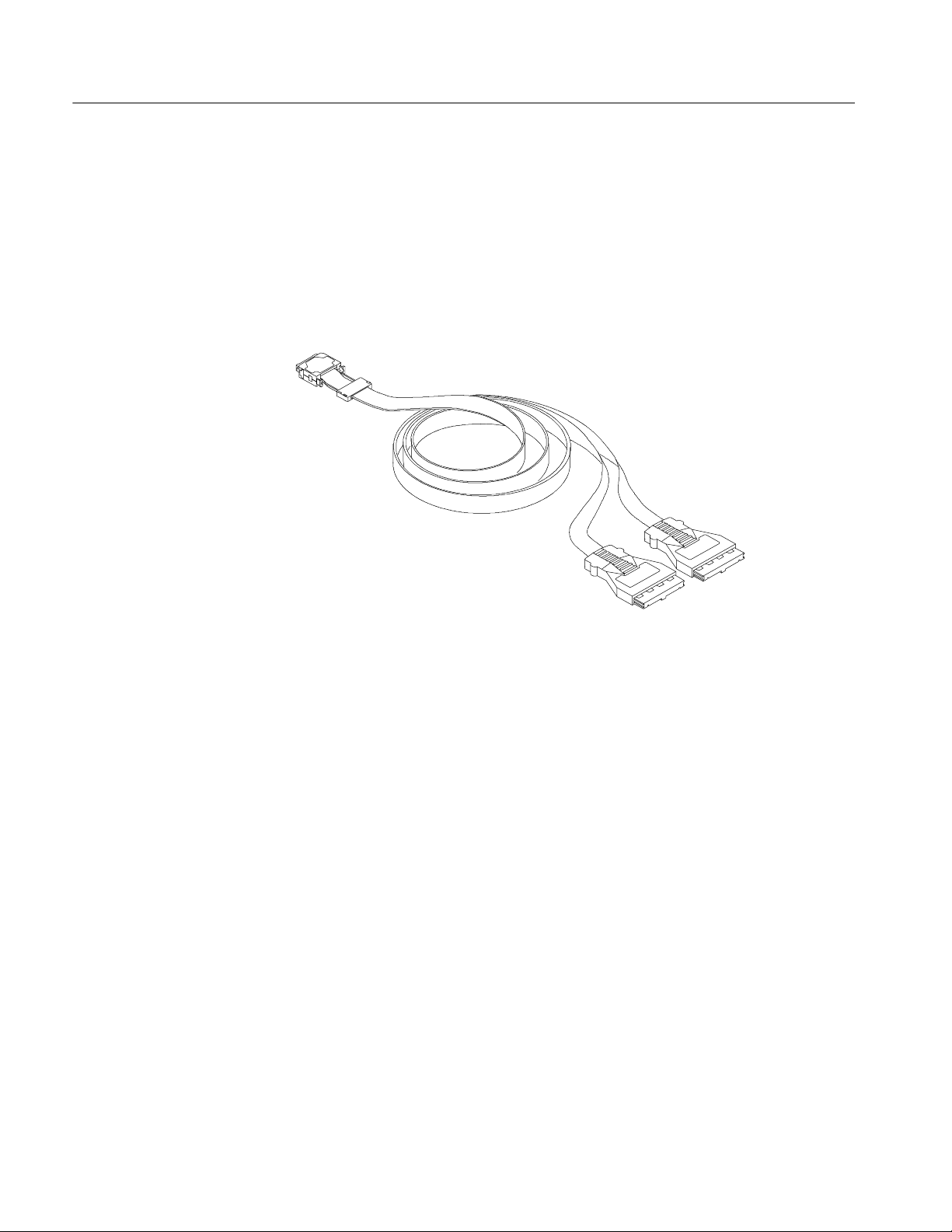
Product Description
The P6434 probe can acquire data from 32 input/output signals and two clocks,
one clock and one qualifier, or two qualifier signals.
The probe has connectors on each end. One end is called the probe tip and
connects to your target system. The other ends are called the module ends and
connect to the logic analyzer. Figure 1 shows the P6434 probe.
Probe-tip
connector
Module-end
connectors
Figure 1: P6434 Mass Termination Probe
2
P6434 Probe Instructions
Page 15
Labels
Operating Basics
The P6434 probe labels are color coded to match the probe connectors on the
logic analyzer. The P6434 probe is shipped with a sheet of labels, a Read This
First sheet, and a P6434 Instructions Manual.
Color Coded Labels
The Table 1 labeling scheme for P6434 probes occurs on most microprocessor
support packages and target systems for signal and channel assignments.
NOTE. Use one Pin 1 label for each probe connector. Do not use two labels with
a pin 1 indicator or two labels without a pin 1 indicator on a single probe.
Table 1: Color coded label combinations (136 and 102 channel module)
Address
ColoronPin1side Tan (CK:0, A3:7--0, A2:7--0)
Color on Pin 38 side Orange (CK:1, A1:7--0, A0:7--0)
Data
ColoronPin1side Blue (QUAL:0, D3:7--0, D2:7--0)
Color on Pin 38 side Yellow (CK:2, D1:7--0, D0:7--0)
Control
ColoronPin1side White (CK:3, C3:7--0, C2:7--0)
Color on Pin 38 side Gray (QUAL:1, C1:7--0, C0:7--0)
Extended (136 channel module only)
ColoronPin1side Green (QUAL:3, E3:7--0, E2:7 --0)
Color on Pin 38 side Violet (QUAL:2, E1:7--0, E0:7--0)
Customizing Labels for a
34 or 68 Channel Module
P6434 Probe Instructions
The labeling scheme for the P6434 probe is shown in Table 2 for a 34 or 68
channel module. Use the extra labels from the label sheet.
Table 2: Color coded label combinations (34 and 68 channel module)
For a 34 channel module
ColoronPin1side(Control) White (CK:3, C3:7--0, C2:7--0)
Color on Pin 38 side (Address) Blank (write in, CK:0, A3:7--0, A2:7--0)
For a 68 channel module
ColoronPin1side(Address) Tan (CK:0, A3:7--0, A2:7--0)
Color on Pin 38 side (Address) Orange (CK:1, A1:7--0, A0:7--0)
ColoronPin1side(Control) White (CK:3, C3:7--0, C2:7--0)
Color on Pin 38 side (Data) Yellow (CK:2, D1:7--0, D0:7--0)
3
Page 16
Operating Basics
Applying Labels
To apply labels to the probe, follow these steps:
1. Locate the labels you need for the P6434 probe from the provided sheet of
labels, but do not peel them off yet. If you need help determining which
labels to use, see steps a and b.
a. Look at the logic analyzer module and determine which channel group
you want to connect the P6434 probe to.
b. Look at the sheet of labels and locate the labels that match the logic
analyzer channel group you need to use. Notice that there are two
different sizes of labels for each channel group.
H Probe-tip labels (smaller)
H Module-end labels (larger)
H Blank labels (custom channel combinations not recommended)
2. Locate the probe-tip end of the P6434 connector (see Figure 2).
Probe tip
Figure 2: Locating the probe-tip connector
3. Locate the pin 1 side of the probe-tip connector by using Figure 3 (end view
of the probe-tip connector).
Metal connector
Note: The position of the bent waves, the angled
ends, are up on the Pin 1 side
Pin1side
Pin38side
Figure 3: End view of the probe-tip connector
4. Remove the pin 1 side label that you need from the sheet of labels.
5. Apply the pin 1 side label to the pin 1 side of the probe-tip connector.
4
P6434 Probe Instructions
Page 17

Operating Basics
NOTE. You can also use the small pin 1 recess or the beveled corners on the
probe tip end of the connector, but both are difficult to find (see Figure 4).
Pin 1 Recess
Beveled corner
Pin1side
Figure 4: Other indicators for pin 1 side
6. Apply the associated pin 38 side label to the probe tip (see Figure 5). If
necessary, see Tables 1 or 2 on page 3 for label information.
Associated probe tip
labels (see Tables 1
and2onpage3)
Pin1side
Pin38side
Figure 5: Location of the pin 38 side label on the probe-tip connector
7. Apply the module-end labels to the module-end connectors (see Figure 6).
To avoid mislabelling, hold the probe-tip connector in your hand and follow
P6434 Probe Instructions
5
Page 18

Operating Basics
the cable to the model-end connector. Match the color of the module-end
label to the probe-tip label.
Match label colors
Module-end label
Probe-tip label
Other side
Match label colors
Figure 6: Applying labels to the module-end connectors
6
P6434 Probe Instructions
Page 19

Connecting the P6434 Probe to the Target System
The P6434 probe can connect to surface-mounted or straddle-mounted Mictor
connectors. You can use the low-profile extender (available as an optional
accessory) to connect the probe to systems with as little as a half inch of
clearance between circuit boards. You can also install optional latch housings
around the connector to provide positive retention of the probe.
In the following procedures, a surface-mounted Mictor connector is shown in the
figures. These procedures are the same for the straddle-mounted connector.
Operating Basics
Direct Connection
To connect the P6434 probe to a Mictor connector in your target system (or on a
TMS probe adapter), follow these steps:
1. Line up the pin 1 indicator on the probe tip with pin 1 on the connector in
your target system. The Mictor connector is keyed to prevent incorrect
connections.
CAUTION. To avoid damaging the probe and target system, always position the
probe perpendicular to the mating connector and gently connect the probe.
Incorrect handling of the probe while connecting it to the target system can
result in damage to the P6434 probe or to the mating connector in the target
system.
NOTE. If you have custom channel combinations for the mictor connector on your
target system, use the blank sheet of labels to create your own pin 1 and pin 38
side labels.
Use one Pin 1 label for each probe connector. Do not use two labels with a pin 1
indicator or two labels without a pin 1 indicator on a single probe.
Custom labeling is an option, though not recommended.
P6434 Probe Instructions
7
Page 20

Operating Basics
2. Position the probe tip perpendicular to the mating connector, and gently
connect the probe as shown in Figure 7.
3. When connected, push down the latch releases on the probe to set the latch.
Push down to latch after
probe is connected
Pin 1
Optional latch housing
Pin 1
Optional latch housing
Pin 1
Push down to latch after
probe is connected
Figure 7: Connecting to a surface- or straddle-mounted connector
4. Connect the module-end connector to the corresponding connector on the
logic analyzer module (match the label colors). The module end is keyed.
8
P6434 Probe Instructions
Page 21

Operating Basics
Low-Profile Extender
Connection
(Optional Accessory)
Low-profile extenders allow you to connect the P6434 probe to systems with as
little as a half inch of clearance between circuit boards. The extender connects to
Mictor connectors with or without a latch housing. The low-profile extender part
number is in the Replaceable Parts List section under Optional Accessories on
page 48.
To connect the probe using the extender, follow these steps:
1. Line up the pin 1 indicator on the low-profile end of the extender with pin 1
on the connector in your target system. The Mictor connector is keyed to
prevent incorrect connections.
2. Position the low-profile end perpendicular to the connector and gently
connect the extender as shown in Figure 8.
3. Connect the P6434 probe by lining up the pin 1 indicator on the P6434 probe
with the pin 1 indicator on the the other end of the extender and connect the
probe to the extender.
4. When connected, push down the latch releases on the probe to set the latch.
Pin 1
Pin 1 (When designing
board, always orient Pin 1
toward edge of board to
direct extender off the
board)
Figure 8: Connecting the low-profile extender
P6434 Probe Instructions
9
Page 22

Operating Basics
P6434 Reduced Bias
Voltage Adapter
Connection
Reduced Bias Voltage adapters allow you to reduce the pull-up voltage that the
P6434 delivers to the system under test. The P6434 Reduced Bias Voltage
adapter connects directly to the Mictor connector or to a low-profile extender.
Refer to the Replaceable Part Lists section under Optional Accessories on page
48 for the Reduced Bias voltage adapter part number.
To connect the probe using the P6434 Reduced Bias Voltage adapter follow these
steps:
1. Line up the pin 1 indicator on the adapter with the pin 1 indicator on the
Mictor connector.
2. Position the adapter perpendicular to the Mictor connector and connect the
adapter as show in Figure 9. The Mictor connector is keyed to prevent
incorrect connections.
3. Line up the pin 1 indicator on the adapter with the pin 1 indicator on the
P6434 probe. Connect the P6434 probe to the adapter.
4. When connected, push down the latch releases on the probe to set the latch.
10
Figure 9: Connecting the Reduced Bias Voltage adapter
If you are using a low-profile extender with the Reduced Bias Voltage adapter
follow the instructions on page 9 to connect the low-profile extender and then,
follow these steps:
1. Line up the pin 1 indicator on the adapter with the pin 1 indicator on the
low-profile extender and connect the adapter to the low-profile extender.
2. Line up the pin 1 indicator on the adapter with the pin 1 indicator on the
P6434 probe, and then connect the probe to the adapter.
P6434 Probe Instructions
Page 23

Operating Basics
3. When connected, push down the latch releases on the probe to set the latch.
Pin 1
Pin 1 (When designing board, always
orient Pin 1 toward edge of board to
direct extender off the board)
Figure 10: Connecting the Reduced Bias Voltage adapter to the low-profile extender
P6434 Probe Instructions
11
Page 24

Operating Basics
Compression-on-PCB to
P6434 Mictor Adapter
Mictor
adapter
Elastomer
holder
Circuit board
Adapter
backing plate
The Compression-on-PCB to P6434 Mictor adapter (see Figure 11) allows the
TLA6xx and TLA7Lx/Mx/Nx/Px/Qx logic analyzers using a P6434 Probe to
take advantage of the new compression footprint and eliminate the need for
Mictor connectors in your target system.
Two different screw lengths are required to accommodate the
0.050-inch -- 0.250-inch (1.27 mm - 6.35 mm) PCB thickness range.
This adapter requires the use of the Compression-on-PCB to P6434 Mictor
adapter land footprint. See Figure 11 for further dimensional information.
32.131 mm
(1.265 in)
15.82 mm
(.623 in)
13.716 mm
(.540 in)
6.35 mm 1.27 mm (.250 in)
(.050 in) PCB Thickness
4.572 mm
(.180 in)
Figure 11: Compression-on-PCB to P6434 Mictor adapter
To compare the clearance between the P6434 Probe connection and the P6434
Probe connection via the Compression-on-PCB to P6434 Mictor adapter refer to
Figure 12 on page 13. Note that the difference in clearance between the P6434
Probe connection and the P6434 Probe connection using the Compression-onPCB to P6434 Mictor adapter is 0.145-inches.
12
P6434 Probe Instructions
Page 25

Operating Basics
P6434
Mictor adapter
32.131 mm
(1.265 in)
15.82 mm
(.623 in)
3.68 mm
(.145 in)
13.716 mm
(.540 in)
34.93 mm
(1.375 in)
Figure 12: Clearance for probe connection using Compression-on-PCB to P6434 Mictor adapter
P6434 Probe Instructions
13
Page 26
Operating Basics
Disconnecting the P6434 Probe from the Target System
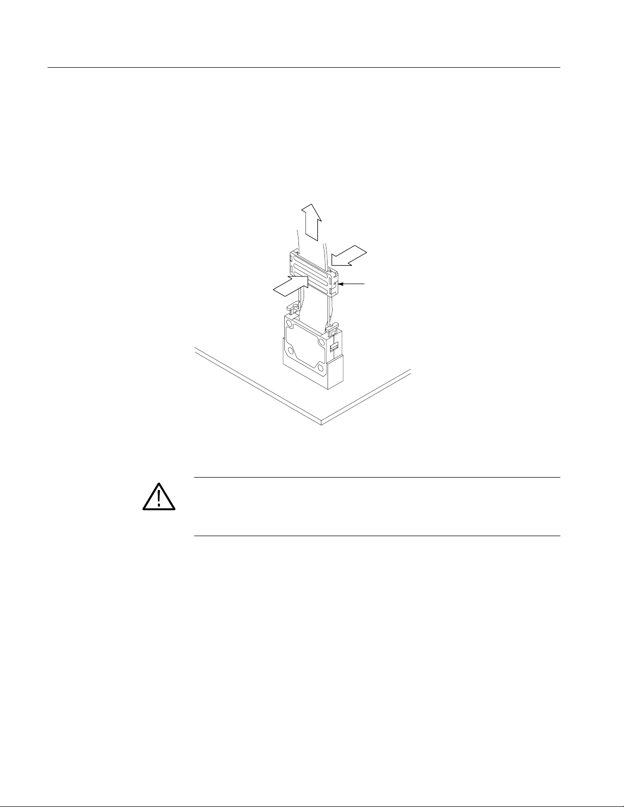
To disconnect the P6434 probe, follow these steps:
1. Gently pull the latch release grip to release the probe tip from the latch
housing as shown in Figure 13.
Grasp sides and
gently pull
Latch release grip
Figure 13: Releasing the probe tip from the latch housing
CAUTION. To avoid damage to the probe and mating connector, hold on to the
latch release grip and gently pull the probe straight out of the connector. Do not
tilt the probe in any direction when disconnecting it. Tilting the probe can
damage the probe and mating connector.
2. Continue to gently pull the probe tip straight out of the mating connector
using the latch release grip.
If you are using an extender, grip the corners of the circuit board end
attached to the target system, and gently pull it straight out of the connector.
14
P6434 Probe Instructions
Page 27
Designing an Interface Between a P6434 Probe and a Target System
This section provides you with some guidelines for designing your own P6434
probe interface on the target system. The guidelines contain information on the
following topics:
H Mictor connectors
H Dimensions and placement of connectors
H Mechanical layout and pinout of connectors
H AMP pinout (preferred)
H Nonstandard pinout (not recommended)
H Probe channel assignments
H Loading and equivalent circuits
Mictor Connectors and Latch Housings
The P6434 probe contains a 38-pin Mictor connector. Table 3 lists Mictor
connectors you can purchase from AMP that are compatible with the probe and
compatible latch housings and connectors from Tektronix.
Table 3: Compatible Mictor connectors
AMP
part number
767054-1* Palladium-nickel plated, surface mount
767044-1* Palladium-nickel plated,straddle mount
-- Latch housing; straddle mount (0.062 inch circuit
-- Latch housing; surface mount
* Preferred
†
See page 48 under Standard Accessories for Tektronix part numbers.
Description
connector (vertical receptacles)
connector(0.062 in circuit board thickness,
right-angle receptacles)
board thickness)
Tektronix
part number
(For quanitites less than
†
27)
(For quanitites less than
†
27)
†
†
P6434 Probe Instructions
15
Page 28

Designing an Interface Between a P6434 Probe and a Target System
You can contact AMP for more detailed information on the Mictor connectors.
For the address, refer to the Replaceable Parts sectiononpage47.
You can purchase latch housing mechanisms to use with Mictor connectors. The
latch housing surrounds the Mictor connector in your target system and provides
positive retention of the P6434 probe.
Figure 14 shows the dimensions of the optional latch housings.
31.50 mm
(1.240 in)
25.40 mm
(1.000 in)
5.08 mm
(.200 in)
.51 mm
(.020 in)
7.11 mm
(.280 in)
28.20 mm
(1.110 in)
25.63 mm
(1.009 in)
1.52 mm
(.060 in)
Figure 14: Latch housing dimensions
12.19 mm
(.480 in)
2.64 mm
(.104 in)
1.40 mm
(.055 in)
9.90 mm
(.390 in)
4.95 mm
(.195 in)
1.27 mm
(.050 in)
3.63 mm (.143 in)
1.42 mm (.056 in)
3.55 mm (.140 in)
Straddle mount
16
NOTE. Refer to the Replaceable Parts List section under Standard Accessories on
page 48 for information on ordering surface-mounted or straddle-mounted latch
housings.
P6434 Probe Instructions
Page 29

Designing an Interface Between a P6434 Probe and a Target System
Dimensions and Placement of Compatible Mictor Connectors
You can use compatible surface-mounted or straddle-mounted Mictor connectors
in your circuit board design. The connectors must be placed as close as possible
to the device under test.
The placement of Mictor connectors depends on whether you plan to connect the
P6434 probe directly to the target system or use the low-profile extender with the
probe.
Direct Connection
Figure 15 shows the dimensions and minimum placement of surface-mounted
connectors on a target system. The side-to-side dimension between connectors
also applies to the straddle-mounted connector.
6.35 mm
(.250 in)
9.90 mm
(.390 in)
Pin 1
31.50 mm
(1.240 in)
31.75 mm
(1.27 in)
10.80 mm
(.51 in)
Figure 15: Dimensions and placement of a surface-mounted Mictor connector with
latch housing
P6434 Probe Instructions
The vertical clearance dimension for the probe is 1.25 inches. Figure 21 on
page 32 shows this dimension.
17
Page 30

Designing an Interface Between a P6434 Probe and a Target System
Low-Profile Extender
Connection
4.953 mm (.195 in)
Optional latch housing
12.19 mm
(.480 in)
10.16 mm
(.400 in)
5.08 mm
(.200 in)
25.40 mm (1.000 in)
When placing Mictor connectors in your target system for use with an extender,
you need to keep one inch of clear space on the pin 1 side from the center of the
Mictor connector in your target system. The vertical clearance for the one inch of
clear space under the extender is 0.2 inches, as shown in Figure 16.
NOTE. Be sure to orient pin 1 on the Mictor connector in your target system to
direct the extender off the board as shown in Figure 8on page 9.
9.52 mm (.375 in) min.
bend radius of cable
2.54 mm (.100 in)
107.95 mm
(4.250 in)
9.90 mm
(.390 in)
Figure 16: Side view and dimensions of the low-profile extender
18
P6434 Probe Instructions
Page 31
Designing an Interface Between a P6434 Probe and a Target System
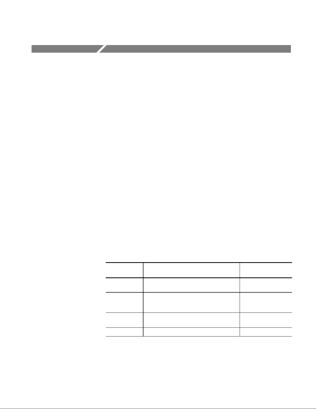
Mechanical Layout and Pin Numbering Sequence of Compatible Mictor Connectors
Each compatible Mictor connector has 43 pins; pins 39 through 43 are grounded.
Pins 1, 2, 37, and 38 are open. Figure 17 shows the positions and spacing between
the pins, the keyhole, and the latch housing mounting holes of a surface-mounted
connector. Table 4 on page 21 shows the recomme nded pin assignments.
Pin 1 Indicator
If you include the latch housing in your design, be sure to place a pin 1 indicator
on your circuit board during design because the latch housing obscures the pin 1
indicator on the Mictor connector. Even though the Mictor connector is keyed,
you still need to know the location of pin 1 when connecting the P6434 probe.
19X 0.43 mm
(.017 in)
18X 0.64 mm
5X 0.89 mm dia.
(.035 .003 in)
Plated through
5X 1.40 mm dia.
(.055 in) Pad both
sides
19.18 mm
(.755 in)
7.62 mm
(.300 in)
10.16 mm
(.400 in)
28.20 mm
(1.110 in)
(.025 in)
.85 mm
(.0335 in)
Pin 1
2.54 mm
(.100 in)
5.08 mm
(.200 in)
6.35 mm
(.250 in)
9.02 mm
(.355 in)
*
2.39 mm dia. (.094 .002 in)
Unplayed through
2X 1.27 mm (.050 in)
2X 2.90 mm
(.114 in)
2X 1.35 mm dia. (.053 .003 in) Plated
through mounting holes for latch housing
2X 2.03 mm dia. (.080 in)
pad both sides
± .076 mm (± .003 in)
tolerance all locations
Notes: * The AMP pin assignment, an industry standard, is what we recommend for your circuit board layouts (see Table 4 on page 21).
Figure 17: Surface-mounted connector layout (component side)
P6434 Probe Instructions
19
Page 32

Designing an Interface Between a P6434 Probe and a Target System
Figure 18 shows the positions and spacing between the pins and latch housing
mounting holes of a straddle-mounted connector.
NOTE. The straddle-mounted connector does not have a keyhole. Be sure to
position pin 1 correctly when building the target system to maintain the correct
mapping of signals from your target system to the logic analyzer probe sections
and channels.
2.80 mm
(.110 in)
1.40 mm
(.055 in)
Note: Original AMP
dimension (.012)
enlarged to allow
for hand insertion
19X Contact pads
both sides
2.28 mm
(.090 in)
1.78 mm (.070 in)
Board edge
.28 mm
(.011 in)
.56 mm
(.022 in)
5X .99 mm dia.
(.039 .003)
Plated through
19.18 mm
(.755 in)
5X 1.40 mm dia.
(.055 in) Pad
both sides
7.62 mm
(.300 in)
10.16 mm
(.400 in)
28.20 mm
(1.110 in)
19X 0.43 mm
(.017 in)
18X 0.64 mm
(.025 in)
0.85 mm
(.0335 in)
Pin 1
2.54 mm
(.100 in)
5.08 mm
(.200 in)
9.02 mm
(.355 in)
2X 1.35 mm dia. (.053 .003 in)
Plated through mounting holes for
latch housing
2.92 mm
(.115 in)
*
2.16 mm
(.085 in)
2X Solder pads
both sides
.81 mm
(.032 in)
± .076 mm (± .003 in)
tolerance all locations
3.73 mm
(.147 in)
Note: * The AMP pin assignment, an industry standard, is what we recommend for your circuit board layouts (see Table 4 on page 21).
Figure 18: Straddle-mounted connector layout (component side)
20
P6434 Probe Instructions
Page 33

Designing an Interface Between a P6434 Probe and a Target System
AMP Probe Channel Assignments (Preferred)
The 17 channels to which the module end connects on the logic analyzer cannot
be changed. When mapping signals from your target system to channels on the
logic analyzer, you must keep the probe section, clock, and/or qualifier channels
together as shown in Tables 1 or 2 on page 3.
Each probe connector has 43 pins; pins 39 through 43 are the five ground pins.
Pins 1, 2, 3, and 4 are unused, and it is recommended that they be connected to
ground.
AMP Pin Assignment
(Preferred)
The preferred pin assignment is the AMP pin assignment (see Table 4), because
other commercial CAD packages use the AMP numbering scheme as the
industry standard. Table 4 shows the pin assignments for the surface-mounted
connector. Pin assignments are the same for the straddle-mounted connector.
AMP uses an odd-side even-side pin assignment. Pin 1 is located at the top left,
and pin 3 is located directly below it. Pin 2 is located on the top right, and pin 4
is located directly below it. Refer to Table 5 on page 22 for the pin assignments.
NOTE. When designing Mictor connectors into your target system, always verify
which pin-numbering sequence your CAD system uses.
Table 4: Preferred pin assignments (AMP) for Mictor connector (component
side)
Type of pin assignment Comments
Pin 1
Pin 3
Preferred
Pin 2
Pin 4
Preferred. This pin assignment is the i ndustry standard
and is what we recommend that you use.
P6434 Probe Instructions
Pin 37
AMP Pin Assignment
Pin 38
21
Page 34

Designing an Interface Between a P6434 Probe and a Target System
AMP
AMP
Tables 5 and 6 show the sections and channels and the P6434 probe pins to
which they connect. Tables 5 and 6 also complies with the labeling schemes in
Tables 1 and 2 on page 3, except for the 34 channel module on the Pin 38 side of
the probe. The Mictor pin numbers are shown for reference only.
NOTE. Table 2 on page 3 shows the labeling scheme for a 34 or 68 channel
module.
Table 5: Pin 1 side probe channel assignments
Section and channel
pin number
5 CLK:0 CLK:3 Q0 Q3
7 A3:7 C3:7 D3:7 E3:7
9 A3:6 C3:6 D3:6 E3:6
11 A3:5 C3:5 D3:5 E3:5
13 A3:4 C3:4 D3:4 E3:4
15 A3:3 C3:3 D3:3 E3:3
17 A3:2 C3:2 D3:2 E3:2
19 A3:1 C3:1 D3:1 E3:1
21 A3:0 C3:0 D3:0 E3:0
23 A2:7 C2:7 D2:7 E2:7
25 A2:6 C2:6 D2:6 E2:6
27 A2:5 C2:5 D2:5 E2:5
29 A2:4 C2:4 D2:4 E2:4
31 A2:3 C2:3 D2:3 E2:3
33 A2:2 C2:2 D2:2 E2:2
35 A2:1 C2:1 D2:1 E2:1
A probe
C probe D probe E probe
37 A2:0 C2:0 D2:0 E2:0
Table 6: Pin 38 side probe channel assignments
Section and channel
pin number
6 CLK:1 Q1 CLK:2 Q2
8 A1:7 C1:7 D1:7 E1:7
A probe
C probe D probe E probe
22
P6434 Probe Instructions
Page 35

Designing an Interface Between a P6434 Probe and a Target System
Table 6: Pin 38 side probe channel assignments (cont.)
AMP
AMP
pin number
pin number
10 A1:6 C1:6 D1:6 E1:6
12 A1:5 C1:5 D1:5 E1:5
14 A1:4 C1:4 D1:4 E1:4
16 A1:3 C1:3 D1:3 E1:3
18 A1:2 C1:2 D1:2 E1:2
20 A1:1 C1:1 D1:1 E1:1
22 A1:0 C1:0 D1:0 E1:0
24 A0:7 C0:7 D0:7 E0:7
26 A0:6 C0:6 D0:6 E0:6
28 A0:5 C0:5 D0:5 E0:5
30 A0:4 C0:4 D0:4 E0:4
32 A0:3 C0:3 D0:3 E0:3
34 A0:2 C0:2 D0:2 E0:2
36 A0:1 C0:1 D0:1 E0:1
38 A0:0 C0:0 D0:0 E0:0
Section and channel
E probeD probeC probeA probe
P6434 Probe Instructions
23
Page 36

Designing an Interface Between a P6434 Probe and a Target System
Nonstandard Probe Channel Assignments (Not Recommended)
The 17 channels to which the module end connects on the logic analyzer cannot
be changed. When mapping signals from your target system to channels on the
logic analyzer, you must keep the probe section, clock, and/or qualifier channels
together as shown in Tables 1 and 2 on page 3.
Each probe connector has 43 pins; pins 39 through 43 are the five ground pins.
Pins 1, 2, 37, and 38 are unused, and it is recommended that they be connected
to ground.
Nonstandard Pin
Assignment
(Not Recommended)
The nonstandard pin assignment was previously used by Tektronix but is no
longer recommended due to incompatibility with other commercial CAD
packages (see Table 7 on page 24).
The pin assignment is counterclockwise with Pin 1 located at the top left, and
pin 2 located directly below it. Pin 20 is located on the bottom right, and pin 21
is located directly above it.
Table 7: Nonstandard pin assignment for Mictor connector (component
side)
Type of pin assignment Comments
Not recommended. This pin assignment was
Not Recommended
Pin 1
Pin 2
Pin 19
Nonstandard Pin Assignment
Pin 21
Pin 20
previously used by Tektronix but is no longer
recommended due to incompatibility with other
commercial CAD packages.
24
Tables 8 and 9 show the sections and channels and the P6434 probe pins to
which they connect. T ables 8 and 9 also comply with the labeling schemes
shown in Tables 1 and 2 on page 3, except for the 34 channel module on the Pin
38 side of the probe. The Mictor pin numbers are shown for reference only.
NOTE. Table 2 on page 3 shows the labeling scheme for a 34 or 68 channel
module.
P6434 Probe Instructions
Page 37

Designing an Interface Between a P6434 Probe and a Target System
*
*
Table 8: Pin 1 side probe channel assignments (nonstandard)
Nonstandard
P6434 probe
pin number
3 CLK:0 CLK:3 Q0 Q3
4 A3:7 C3:7 D3:7 E3:7
5 A3:6 C3:6 D3:6 E3:6
6 A3:5 C3:5 D3:5 E3:5
7 A3:4 C3:4 D3:4 E3:4
8 A3:3 C3:3 D3:3 E3:3
9 A3:2 C3:2 D3:2 E3:2
10 A3:1 C3:1 D3:1 E3:1
11 A3:0 C3:0 D3:0 E3:0
12 A2:7 C2:7 D2:7 E2:7
13 A2:6 C2:6 D2:6 E2:6
14 A2:5 C2:5 D2:5 E2:5
15 A2:4 C2:4 D2:4 E2:4
16 A2:3 C2:3 D2:3 E2:3
17 A2:2 C2:2 D2:2 E2:2
Section and channel
A probe C probe D probe E probe
18 A2:1 C2:1 D2:1 E2:1
19 A2:0 C2:0 D2:0 E2:0
* These pin numbers were previously used by Tektronix but are no longer recom-
mended due to incompatibility with other commercial CAD packages.
Table 9: Pin 38 side probe channel assignments (nonstandard)
Nonstandard
P6434 probe
pin number
36 CLK:1 Q1 CLK:2 Q2
35 A1:7 C1:7 D1:7 E1:7
34 A1:6 C1:6 D1:6 E1:6
33 A1:5 C1:5 D1:5 E1:5
32 A1:4 C1:4 D1:4 E1:4
31 A1:3 C1:3 D1:3 E1:3
30 A1:2 C1:2 D1:2 E1:2
Section and channel
A probe C probe D probe E probe
25
P6434 Probe Instructions
Page 38

Designing an Interface Between a P6434 Probe and a Target System
Table 9: Pin 38 side probe channel assignments (nonstandard) (cont.)
Nonstandard
P6434 probe
P6434 probe
pin number *
pin number *
29 A1:1 C1:1 D1:1 E1:1
28 A1:0 C1:0 D1:0 E1:0
27 A0:7 C0:7 D0:7 E0:7
26 A0:6 C0:6 D0:6 E0:6
25 A0:5 C0:5 D0:5 E0:5
24 A0:4 C0:4 D0:4 E0:4
23 A0:3 C0:3 D0:3 E0:3
22 A0:2 C0:2 D0:2 E0:2
21 A0:1 C0:1 D0:1 E0:1
20 A0:0 C0:0 D0:0 E0:0
* These pin numbers were previously used by Tektronix but are no longer recom-
mended due to incompatibility with other commercial CAD packages.
Section and channelNonstandard
E probeD probeC probeA probe
26
P6434 Probe Instructions
Page 39
Loading and Equivalent Circuits
The load presented to the target system by the P6434 probe is low. The load is
equivalent to a 2 pF capacitance with 20 kΩ resistance returned to a 2.2 V
supply. The following approximation of the probe loading is sufficient for most
circuit simulation calculations.
Figure 19 shows the equivalent circuit of the P6434 probe. Table 10 shows the
values you can use to calculate characteristics of the lossy delay lines shown in
the next two figures.
Table 10: Lossy delay line values
Characteristic Value
C (capacitance) 1.58 pF per inch
L (inductance) 8.9 nH per inch
R (resistance) 0.067 Ω per inch
Designing an Interface Between a P6434 Probe and a Target System
Z0(impedance) 75 Ω
1.6 nH
0.7 pF
0.005
Ω
Mictor connector
equivalent circuit
1.6 nH
0.005
Ω
1.1 pF
Figure 19: Equivalent circuit for the P6434 probe
0.23 pF
20 kΩ
LOSSY
Length = 58 inches
75
Ω
+2.2 V
P6434 Probe Instructions
27
Page 40

Designing an Interface Between a P6434 Probe and a Target System
The low-profile extender used with the P6434 probe increases the load. The
additional load is equivalent to a 100 Ω resistor connected in series with
approximately three inches of 75 Ω coaxial cable to the probe tip.
Although the extender can increase the loading significantly, using the extender
might be necessary in situations where there is as little as half an inch of
clearance.
The extender is useful in a target system where signal risetimes are greater than
one or two nanoseconds. Faster risetimes cause transmission line reflections on
signals.
Figure 20 shows the equivalent circuit for the P6434 probe with a low-profile
extender
Mictor connector equivalent circuit Mictor connector equivalent circuit
0.7 pF
1.6 nH
1.1 pF
0.005 Ω
1.6 nH
0.005 Ω
0.23 pF
20 kΩ
LOSSY
100 Ω
Length = 3 in
Length = 58 in
1.6 nH
LOSSY
Figure 20: Equivalent circuit for the P6434 probe with a low-profile extender
0.005 Ω
0.7pF
1.6 nH
0.005 Ω
75 Ω
+2.2 V
28
P6434 Probe Instructions
Page 41
Reference
Maintenance
This section contains information on the following topics and tasks:
H Probe maintenance
H Probe circuit description
H Specifications
H Disassembly and reassembly procedures
H Functional verification procedure
The P6434 probe does not require scheduled or periodic maintenance. To
maintain good electrical contact, keep the probe free of dirt, dust, and
contaminants. Also, ensure that any electrically conductive contaminants are
removed.
Dirt and dust can usually be removed with a soft brush. For more extensive
cleaning, use only a damp cloth. Abrasive cleaners and organic solvents should
never be used.
CAUTION. To prevent damage, service the probe only in a static-free environment.
The component devices contained on the P6434 probe are susceptible to
static-discharge damage.
If the probe is connected to the target system, grasp the ground connector on the
back of the logic analyzer to discharge your stored static electricity. If the probe
is not connected, touch the antistatic bag to discharge stored static electricity
from the probe.
Always wear a grounding wrist strap, or similar device, while servicing the
probe.
If you connect and disconnect the P6434 probe frequently, occasionally use a
magnifying glass to examine the contact points on both the probe tip and on the
mating connector. If contacts have been dislocated from their proper position,
P6434 Probe Instructions
29
Page 42

Reference
Circuit Description
Specifications
you can use a pair of small tweezers (such as a #3 to #5), to carefully move the
contacts back into place.
The P6434 probe contains 34 sets of signal connections (32 used as data
channels and two used as clock or qualifier channels). The probe tip connection
is a 38-pin Mictor connector by AMP, Inc. Each signal line has a 20 kΩ ± 1%
resistor (shunted by a 0.23 pF capacitor) in series with an approximately five
foot long section of 75 Ω coaxial cable.
These specifications are for a P6434 probe connected between a compatible
Tektronix logic analyzer and a target system. Table 11 shows the electrical
requirements of the P6434 probe.
Table 11: Electrical specifications
Characteristics Requirements
Number of input channels 34 (32 data and 2 clock/qualifier channels)
Input impedance
Threshold accuracy
Channel-to-channel skew <150 ps
Delay time from probe tip to module end 7.33 ns (The approximate length of the probe
Max. operating swing time 8 V peak-to-peak
Probe overdrive
Max. nondestructive input signal to probe
Max. sync clock rate 200 MHz in full speed mode (5 ns between
Min. sampling period 4 ns (0.5 ns w/MagniVu)
Measured typical signal loading* AC load DC load
* The 20 kΩ resistor is returned to +2.2 V.
20 kΩ ±1% in parallel with 2 pF ± 0.2 pF
±100 mV
is 1.6 m or 62 in.)
The greater of ± 300 mV or ± 25% of signal
swing
±15 V
active clock edges)
≈2pF ≈20 kΩ*
30
P6434 Probe Instructions
Page 43
Table 12 shows the environmental specifications.
Table 12: Environmental specifications
Reference
Characteristic
Temperature
Maximum operating +50 ° C (+122 ° F)[
Minimum operating 0 ° C(+32° F)
Non-operating -- 5 5 ° Cto+75° C(--67° F to +167 ° F)
Humidity 10 to 95% relative humidity
Altitude
Operating 4.5 km (15,000 ft) maximum
Non-operating 15 km (50,000 ft) maximum
* Designed to meet Tektronix standard 062-2847-00 class 5.
[
Not to exceed target system thermal considerations. Forced air cool ing might be
required.
Description*
Table 13 shows the certifications and compliances that apply to the P6434 probe.
Table 13: Certifications and compliances
Category Standards or description
EC Compliance There are no current European Directives that
apply to this product.
P6434 Probe Instructions
31
Page 44

Reference
Figure 21 shows the vertical dimensions of the P6434 probe and low-profile
extender.
31.75 mm
(1.250 in)
5.08 mm
(.200 in)
10.16 mm
(.400 in)
Figure 21: Vertical dimensions of the P6434 probe and low- profile extender
Figure 22 shows the vertical dimensions of the P6434 probe and Reduced Bias
Voltage adapter.
62.23 mm
(2.45 in)
32
Figure 22: Vertical dimensions of the P6434 probe and Reduced Bias Voltage
Adapter
P6434 Probe Instructions
Page 45

Disassembling the Probe
The following procedures describe disassembling the P6434 probe. If you are
installing the connector parts replacement kit, follow the Probe Tip procedures
on pages 33 and 36. If you are installing either of the cable replacement kits, you
must also perform the Latch Release Grip and Module End procedures.
Reference
Probe Tip
To disassemble the probe tip, follow these steps (refer to Figure 23 as a guide):
Remove screws (4)
Elastomer connectors (2)
Circuit boards (2)
P6434 Probe Instructions
Figure 23: Disassembling the P6434 probe tip
1. Remove the four screws from the outside of the probe case using a
0.050-inch hexagonal screwdriver, and open the case halves.
2. Gently remove the two small circuit boards and cables from the plastic
holder. The small circuit boards are held in place by two tab features in the
plastic holder.
The circuit boards hold the elastomer connectors (which are very small) in
place. When you remove the circuit boards, the elastomer connectors may
fall out of the probe.
33
Page 46

Reference
CAUTION. To prevent damage to the elastomer, use tweezers and handle the
elastomer connectors on the flat areas adjacent to the gold plated contact pads.
The elastomer connectors are very small and are susceptible to contamination by
natural skin oils and mishandling.
3. Using tweezers on the flat areas adjacent to the gold plated contact pads,
remove the elastomer connectors. See Figure 27 on page 37.
4. If you are installing either the pin 1 or pin 38 cable kit, follow the Latch
Release Grip and Module End disassembly procedures on pages 34 and 35.
5. If you are only installing the connector parts replacement kit, follow the
Probe Tip procedure on page 36.
Latch Release Grip
To disassemble the latch release grip, follow these steps:
1. Use two small, flat-bladed screwdrivers in the slots opposite the tabs on each
side of the grip as shown in Figure 24.
2. With thumbs placed lightly on the tabs to be released, pry the grip open by
carefully levering the screwdrivers down. Do not overstress the tabs beyond
deflection required to release the tabs.
When you open the latch release grip, the latch release cord comes out of the
grip, thereby detaching the grip from the latch release on the probe.
Latch release cords
Slots
34
Latch release grip
Figure 24: Disassembling the latch release grip
P6434 Probe Instructions
Page 47

Reference
Module End
To disassemble the module end of the probe, refer to Figure 25 and follow these
steps:
1. On the module end, remove the four screws from the outside of the
connector housing using a 0.050-inch hexagonal screwdriver, and open the
housing.
2. Remove the cable with the connector attached.
3. Remove the trim pieces from the connector housing.
Label
Cable and
connector
Screws (4)
Figure 25: Disassembling the module end
Trim pieces
P6434 Probe Instructions
35
Page 48

Reference
Reassembling the Probe
Use the following procedures to reassemble the P6434 probe.
NOTE. When reassembling the probe, you must use both the new board holder
and both elastomer connectors included with the service kit. These components
have design improvements that must be replaced as a set.
Probe Tip
To reassemble the probe tip, refer to Figure 26 and follow these steps:
1. If you are reusing the Mictor connector circuit board, remove the old board
holder.
2. Install the Mictor connector circuit board into the new board holder.
Remove Install
Relieve pressure on
detents to remove
Detents
Relieve pressure on
detents to remove
Board holder
Figure 26: Mictor connector circuit board and board holder
Press until detents snap
together
Board holder
36
3. Lay the Mictor board assembly on a flat surface with the pin 1 side of the
connector facing up. See Figure 28 on page 37 for the correct orientation.
CAUTION. To prevent damage to the elastomer, use tweezers and handle the
elastomer connectors on the flat areas adjacent to the gold plated contact pads.
The elastomer connectors are very small and are susceptible to contamination by
natural skin oils and mishandling.
4. Using tweezers on the flat areas on both sides of the gold plated contact
pads, carefully orient the elastomer connector, and place it in the elastomer
slot in the board holder as shown in Figure 27.
P6434 Probe Instructions
Page 49

Reference
Gold plated
contact pads
Elastomer
Elastomer
Ledge
Tweezer
Elastomer
slot
Ledge
Figure 27: Positioning the elastomer connector
5. Place the circuit board attached to the pin 1 cable into the back (cable side)
of the board holder as shown in F igure 28.
6. Press the front (connector side) of the circuit board attached to the cable
down until it snaps into place in the board holder.
Pin 1 indicator
Board holder
Align the back edge first, and then
snap the front edge into place
Pin 1 cable
Figure 28: Positioning the circuit board in the probe
7. Turn the probe over and repeat steps 4 through 6 for the pin 38 side of the
probe.
P6434 Probe Instructions
37
Page 50

Reference
8. Position a latch release on each side of the case half. See Figure 29.
Latch Release Grip
Figure 29: Reattaching the latch releases and case halves
9. Align the pin 1 case half with the pin 1 side of the connector, attach the case
halves, and reconnect the screws as shown in Figure 29.
To reassemble the latch release grip, follow these steps:
1. Place the latch release cords into the latch releases as shown in Figure 30.
2. Push the latch release downward to force the latch release cord to snap
through the slot and into the small hole.
38
P6434 Probe Instructions
Page 51

Reference
Latch release fits
between these flanges
Figure 30: Reattaching the latch release cords to the latch releases
3. Place the other end of the latch release cords into the latch release grip and
reconnect the latch release grip as shown in Figure 31.
P6434 Probe Instructions
Figure 31: Reconnecting the latch r elease cords to the latch release grip
4. You may need to reapply labels. Refer to the description of Labels on page 3
for information on how to apply labels.
39
Page 52

Reference
Module End
To reassemble the module end of the probe, follow these steps:
1. If you are installing either the pin 1 or pin 38 cable kit, follow the procedure
to reassemble the probe tip.
2. On the module end, position the trim pieces in the connector housing as
shown in Figure 32.
Label
Connector
key
Trim pieces
Figure 32: Reassembling the module end
3. Orient the nonkeyed side of the connector to the case half with the label, and
position the connector in the case halves.
4. Attach the case halves and reconnect the screws as shown in Figure 32.
5. You may need to reapply labels. Refer to the description of Labels on page 3
for information on how to apply labels.
40
P6434 Probe Instructions
Page 53
Functional Verification
Reference
This procedure checks the basic functionality of the probe by verifying that the
probes recognize signal activity at the probe tips. No calibration is necessary.
The functional verification procedure for the P6434 probe requires the following
test equipment:
H Adjustment and verification test fixture (refer to the Replaceable Parts List
section under Optional Accessories on page 48 for part number information)
H Power supply for the test fixture (refer to the Replaceable Parts List section
under Optional Accessories on page 48 for part number information)
H Logic analyzer mainframe
H Logic analyzer module
To perform the functional verification procedure, follow these steps:
1. Connect the module ends of the P6434 probe to the logic analyzer module.
2. Connect the probe tip to J5 on the the test fixture as shown in Figure 33.
J15
Figure 33: Jumper and connector locations on the test fixture
3. Place J15 in the INT position to select the internal 50 MHz clock.
J5
P6434 Probe Instructions
4. Connect the power adapter to the test fixture and power on the test fixture.
5. Power on the logic analyzer.
41
Page 54

Reference
6. Verify that the logic analyzer passes the power-on diagnostics.
7. Go to the Setup menu for the logic analyzer module to which the probes are
connected.
8. Click the Set Thresholds button to display the threshold settings. Set the
threshold for all channels to be 700 mV. Close the Probes Threshold dialog
box and click Set All.
9. Click the Show Activity button to display the Activity Indicator dialog box.
10. Visually verify that the Activity Indicator dialog box shows activity on all
probe channels that are connected to the test fixture (see Figure 34).
Note the signal activity for the clock, qualifier and data channels for the C3,
C2, C1, and C0 probe sections. Also note that there is no activity on other
probe sections because the probes are not connected to a signal source. (The
channels are all high.)
No activity
(high)
42
Stuck low
(No activity)
Signal activity
on all connected
channels
Stuck high
(No activity)
Figure 34: Example of the Activity Indicator dialog box
11. Visually verify in the Activity Indicator dialog box that none of the
connected channels are stuck high or stuck low (see Figure 34).
CAUTION. To prevent damage to the test fixture connector, grasp the mictor
connector on the test fixture when wiggling the probe tip end.
P6434 Probe Instructions
Page 55

Reference
To check for intermittent failures, gently wiggle each of the three probe ends.
The test fixture only checks for open channels; therefore, if channels are
shorted together, these channels will appear as connected signal activity on
the test fixture.
12. Repeat this procedure for additional probes.
13. Close the Show Activity widow.
14. Return the threshold levels to their former values in the Probe Threshold
window.
This completes the functional verification.
P6434 Probe Instructions
43
Page 56

Reference
44
P6434 Probe Instructions
Page 57

Replaceable Parts
This chapter contains a list of the replaceable components for the P6434 Probe.
Use this list to identify and order replacement parts.
Parts Ordering Information
Replacement parts are available through your local Tektronix field office or
representative.
Changes to Tektronix products are sometimes made to accommodate improved
components as they become available and to give you the benefit of the latest
improvements. Therefore, when ordering parts, it is important to include the
following information in your order:
H Part number
H Instrument type or model number
H Instrument serial number
H Instrument modification number, if applicable
If you order a part that has been replaced with a different or improved part, your
local Tektronix field office or representative will contact you concerning any
change in part number.
Using the Replaceable Parts List
The tabular information in the Replaceable Parts List is arranged for quick
retrieval. Understanding the structure and features of the list will help you find
all of the information you need for ordering replacement parts. The following
table describes the content of each column in the parts list.
P6434 Probe Instructions
45
Page 58

Replaceable Parts
Parts list column descriptions
Column Column name Description
1 Figure & index number Items in this section are referenced by figure and i ndex numbers to the exploded view
illustrations that follow.
2 Tektronix part number Use this part number when ordering replacement parts from Tektronix.
3 and 4 Serial number Column three indicates the serial number at which the part was first effective. Column four
indicates the serial number at which the part was discontinued. No entries indicates the part is
good for all serial numbers.
5 Qty This indicates the quantity of parts used.
6 Name & description An item name is separated from the description by a colon (:). Because of space limitations, an
item name may sometimes appear as incomplete. Use the U.S. Federal Catalog handbook
H6-1 for further item name identification.
7 Mfr. code This indicates the code of the actual manufacturer of the part.
8 Mfr. part number This indicates the actual manufacturer’s or vendor’s part number.
Abbreviations
Chassis Parts
Mfr. Code to Manufacturer
Cross Index
Abbreviations conform to American National Standard ANSI Y1.1--1972.
Chassis-mounted parts and cable assemblies are located at the end of the
Replaceable Electrical Parts List.
The table titled Manufacturers Cross Index shows codes, names, and addresses
of manufacturers or vendors of components listed in the parts list.
46
P6434 Probe Instructions
Page 59

Replaceable Parts
Manufacturers cr oss index
Mfr.
code
80009 TEKTRONIX INC 14150 SW KARL BRAUN DR
00779
0GV90 GLOBTEK INC 186 VETERANS DRIVE NORTHVALE, NJ 07647--2303
60381 PRECISION INTERCONNECT CORP. 16640 SW 72ND AVE PORTLAND, OR 97224
Manufacturer Address City, state, zip code
BEAVERTON, OR 97077-- 0001
HARRISBURG, PA 17105--3608
AMP INC.
PO BOX 500
CUSTOMER SERVICE DEPT
PO BOX 3608
Replaceable parts list
Fig. &
index
number
25--0 010-6434-01 1 PROBE; P6434 MASS TERMINATION; 34 CHANNEL 80009 010-6434-01
Tektronix part
number
Serial no.
effective
Serial no.
discont’d
Qty Name & description
Mfr.
code
Mfr. part number
118-9479-00 1 SERVICE KIT; MECHANICAL PARTS INCLUDES: 80009 118-9479-00
--1 1 LABEL SHEET; PROBE TIP AND MODULE ENDS, P6434
--2 4 SCREWS, #1--72 x 0.375 BUTTON HEAD
--3 4 NUTS, #1--72 HEX
--4 2 PROBE TIP CASE HALVES
--9 2 PULL GRIP HALVES
--10 1 MODULE END CASE HALF, TOP
--11 2 TRIM, CONNECTOR HOUSING
--12 1 MODULE END CASE HALF, BOTT OM
--13 4 SCREWS, #2--56 x 0.187 BUTTON HEAD
--14 2 PULL CORDS
--15 2 LATCH RELEASES
118-9477-01 1 SERVICE KIT; CABLE PARTS;PIN 1 SIDE INCLUDES: 80009 118-9477-01
--5 2 ELASTOMER CONNECTORS
--6 1 BOARD HOLDER; MOLDED
--7 1 PIN 1 SIDE CABLE WITH CIRCUIT BOARD
--9 2 PULL GRIP HALVES
--14 2 PULL CORDS
1 KIT INSTRUCTIONS
118-9487-01 1 SERVICE KIT; CABLE PARTS; PIN 38 SIDE INCLUDES: 80009 118-9487-01
--5 2 ELASTOMER CONNECTORS
--6 1 BOARD HOLDER; MOLDED
--8 1 PIN 38 SIDE CABLE WITH CIRCUIT BOARD
--9 2 PULL GRIP HALVES
P6434 Probe Instructions
47
Page 60

Replaceable Parts
Replaceable parts list (cont.)
Fig. &
index
number
-- 1 4 2 PULL CORDS
--5 2 ELASTOMER CONNECTORS
--6 1 BOARD HOLDER; MOLDED
--16 1 MICTOR CONNECTOR CKT BD W MICTOR CONNECTOR
Tektronix part
number
118-9478-01 1 SERVICE KIT; CONNECTOR PARTS INCLUDES: 80009 118-9478-01
070-9793-XX 1 MANUAL,TECH:INSTRUCTION, P6434 PROBE 80009 070-9793-XX
105-1088-00 * 1 LATCH HOUSING; STRADDLE MOUNT (NOT SHOWN) 80009 105-1088-00
105-1089-00 * 1 LATCH HOUSING; SURFACE MOUNT (NOT SHOWN) 80009 105-1089-00
Serial no.
effective
Serial no.
discont’d
Name & descriptionQty
1 KIT INSTRUCTIONS
1 KIT INSTRUCTIONS
STANDARD ACCESSORIES
Mfr.
code
Mfr. part number
131--6134-01
131-6520-00
--17 010-0612-00 1
--18 671-5481-00 1 P6434 REDUCED BIAS VOLTAGE ADAPTER 80009 671-5481-00
--19 020-2455-00 1 17CH COMPRESSION-ON--PCB TO P6434 MICTOR
--20 020-2456-00 1 34CH COMPRESSION-ON--PCB TO P6434 MICTOR
671-3599-01 1 ADJUSTMENT/VERIFICATION TEST FIXTURE 80009 671-3599-01
119-4855-00 1 POWER SUPPLY (U S):18W,WALL MOUNT,120VAC 60HZ
119-4856-00 1 POWER SUPPLY (EC ):18W,WALL MOUNT,220VAC 50HZ
119-4859-00 1 POWER SUPPLY (J P):18W,WALL MOUNT,100VAC 60HZ
*Contact your Tektronix representative for pricing of larger q uantities of latch housings or Precision Interconnect as listed in the manufacturers cross index.
†
Order from Tektronix for quantities smaller than 27; if larger, from AMP,INC as listed in the manufacturers cross index.
†
†
CONN,RCPT:SMD,MICTOR,FEMALE,STR,38 POS,0.025
CTR,0.240 H,PALLADIUM NICKEL,IMPEDANCE MATCH (NOT
SHOWN)
CONN,RCPT:EDGE MOUNT,MICTOR,FEMALE,RTANG,38
POS,0.025 CTR,PD NI,MATCHED IMPEDANCE (NOT
SHOWN)
OPTIONAL ACCESSORIES
LOW-- PROFILE EXTENDER, 4.25 INCH OVERALL
ADAPTER
ADAPTER
INPUT,12VDC 1.5A OUTPUT,UNREGULATED,183CM
CABLE,STR C (NOT SHOWN)
INPUT,12VDC 1.5A OUTPUT,UNREGULATED,183CM
CABLE,STR C (NOT SHOWN)
INPUT,12VDC 1.5A INPUT,UNREGULATED,183CM
CABLE,STR CO (NOT SHOWN)
TK0AT 767054--1
TK0AT 767044--1
80009 010-0612-00
80009 020-2455-00
80009 020-2456-00
0GV90 WD1E1500C12CP
0GV90 WD13E1500C12CP
0GV90 WD49E1500C12CP
48
P6434 Probe Instructions
Page 61

Replaceable Parts
2
1
3
16
Pin 1
14
15
5
6
Pin38side
4
Pin1side
The cable kits are not interchangeable. Be sure
to order the correct kit number for items 7 or 8.
7
8
9
10
11
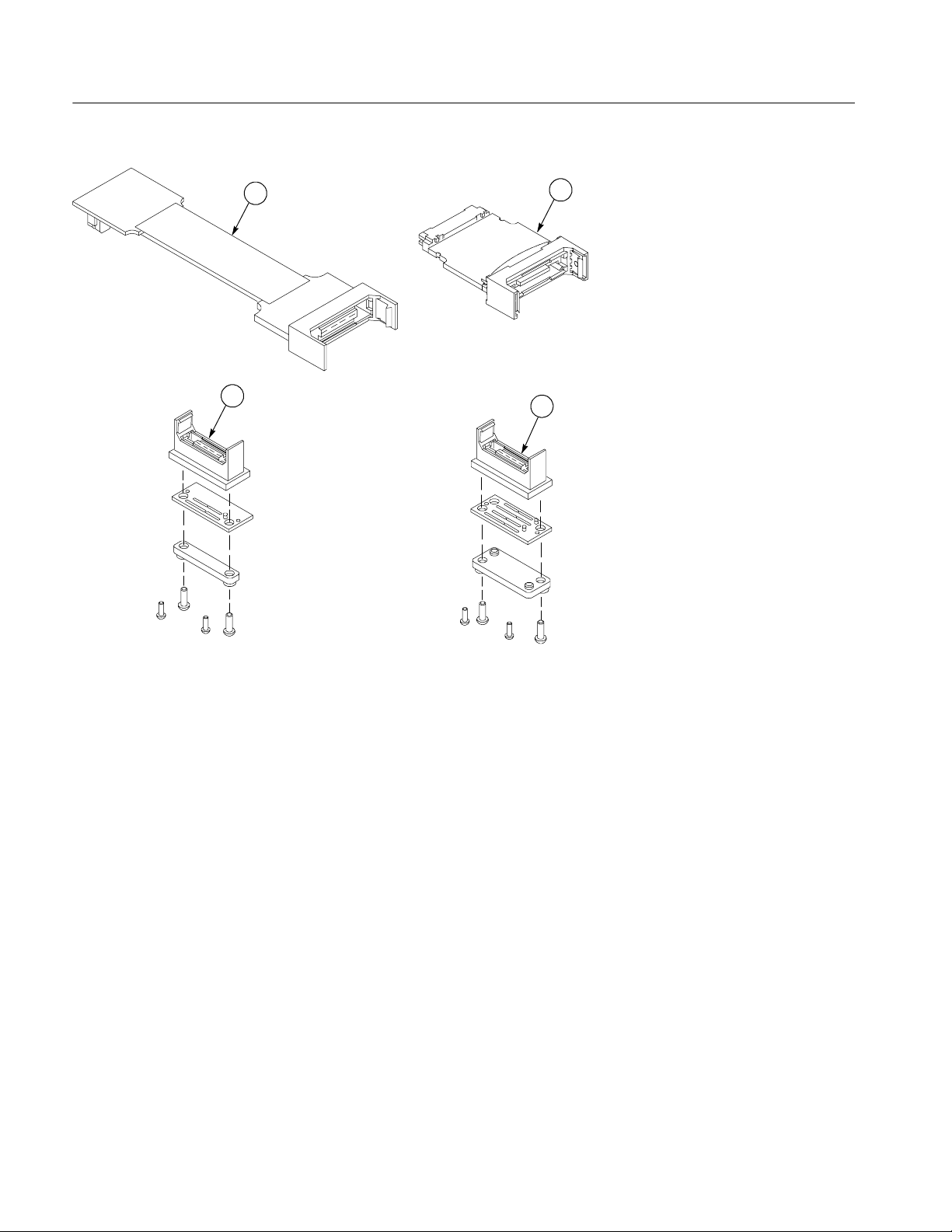
Figure 35: P6434 probe exploded view
P6434 Probe Instructions
13
12
49
Page 62
Replaceable Parts
19
17
18
20
Figure 36: Optional accessories
50
P6434 Probe Instructions
 Loading...