

Page 1

Instructions
P6419
Logic Analyzer Probe
071-1303-00
www.tektronix.com
*P071130300*
071130300
Page 2

Copyright © Tektronix, Inc. All rights reserved. Licensed software products are owned by Tektronix or its suppliers and
are protected by United States copyright laws and international treaty provisions.
Use, duplication, or disclosure by the Government is subject to restrictions as set forth in subparagraph (c)(1)(ii) of the
Rights in Technical Data and Computer Software clause at DFARS 252.227-7013, or subparagraphs (c)(1) and (2) of the
Commercial Computer Software -- Restricted Rights clause at FAR 52.227-19, as applicable.
Tektronix products are covered by U.S. and foreign patents, issued and pending. Information in this publication supercedes
that in all previously published material. Specifications and price change privileges reserved.
Tektronix, Inc., 14200 SW Karl Braun Drive, Beaverton, OR 97077
TEKTRONIX, TEK, TLAVu, PatGenVu, and MagniVu are registered trademarks of Tektronix, Inc.
Page 3

HARDWARE WARRANTY
Tektronix warrants that the products that it manufactures and sells will be free from defec ts in materials and workmanship
for a period of one (1) year from the date of shipment. If a product proves defective during this warranty period, Tektronix,
at its option, either will repair the defective product without charge for parts and labor, or will provide a replacement in
exchange for the defective product.
In order to obtain service under this warranty, Customer must notify Tektronix of the defect before the expiration of the
warranty period and make suitable arrangements for the performance of service. Customer shall be responsible for
packaging and shipping the defective product to the service center designated by Tektronix, with shipping charges prepaid.
Tektronix shall pay for the return of the product to Customer if the shipment is to a location within the country in which the
Tektronix service center is located. Customer shall be responsible for paying all shipping charges, duties, taxes, and any
other charges for products returned to any other locations.
This warranty shall not apply to any defect, failure or damage caused by improper use or improper or inadequate
maintenance and care. Tektronix shall not be obligat ed to furnish service under this warranty a) to repair damage resulting
from attempts by personnel other than Tektronix representatives to install, repair or service the product; b) to repair
damage resulting from improper use or connection to incompatible equipment; c) to repair any damage or malfunction
caused by the use of non-Tektronix supplies; or d) to service a product that has been modified or integrated with other
products when the effect of such modification or integration increases the time or difficulty of servicing the product.
THIS WARRANTY IS GIVEN BY TEKTRONIX IN LIEU OF ANY OTHER W ARRANTIES, EXPRESS OR
IMPLIED. TEKTRONIX AND ITS VENDORS DISCLAIM ANY IMPLIED WARRANTIES OF
MERCHANTABILITY OR FITNESS FOR A PARTICULAR PURPOSE. TEKTRONIX’ RESPONSIBILITY TO
REPAIR OR REPLACE DEFECTIVE PRODUCTS IS THE SOLE AND EXCLUSIVE REMEDY PROVIDED TO
THE CUSTOMER FOR BREACH OF THIS WARRANTY. TEKTRONIX AND ITS VENDORS WILL NOT BE
LIABLE FOR ANY INDIRECT, SPECIAL, INCIDENTAL, OR CONSEQUENTIAL DAMAGES IRRESPECTIVE
OF WHETHER TEKTRONIX OR THE VENDOR HAS ADV ANCE NOTICE OF THE POSSIBILITY OF SUCH
DAMAGES.
Page 4

Page 5

Table of Contents
Operating Basics
General Safety Summary v...................................
Preface vii...................................................
Related Documentation vii...........................................
Contacting Tektronix viii.............................................
Product Description 1........................................
Mictor-on-PCB to Compression Adapter 2..............................
Compression-on-PCB to P6434 Mictor Adapter 3........................
Attaching Probe Labels 5.....................................
Connecting the Probes to the Logic Analyzer 7...................
Cleaning the P6419 Compression Footprints 8...................
Cleaning the P6419 Probe Heads 8.............................
Storing the P6419 Probe Heads 9..............................
Connecting the Probes to the Target System 10....................
Connecting the P6419 High Density Probes 10...........................
Connecting the Mictor-on-PCB to Compression Adapter 13.................
Connecting the Compression-on-PCB to P6434 Mictor Adapter 13...........
Reference
Maintenance
Designing an Interface Between the P6419 Probe and a Target
System 15................................................
Signal Fixturing Considerations 15.....................................
Signal Names 19...................................................
Land Footprints 27..................................................
Mechanical Considerations 30........................................
Special Considerations 33............................................
Physical Attachment Requirements for P6419 probes 33....................
Physical Attachment Requirements for the Compression-on-PCB to P6434
Mictor and Mictor-on-PCB to Compression Adapters 35................
Electrical Considerations 35..........................................
Transmission Lines 35...............................................
P6419 High-Density Probe Load Model 36..............................
Specifications 38.............................................
Probe Calibration 41.........................................
Functional Check 41..........................................
Inspection and Cleaning 41....................................
P6419 Probe Service Procedures 42.............................
Repackaging Instructions 42...................................
P6419 Logic Analyzer Probe Instructions
i
Page 6

Table of Contents
Replaceable Parts
Index
Parts Ordering Information 43.................................
Using the Replaceable Parts List 43.............................
ii
P6419 Logic Analyzer Probe Instructions
Page 7

List of Figures
Table of Contents
Figure 1: P6419 logic analyzer probe 1..........................
Figure 2: Mictor-on-PCB to Compression adapter 2..............
Figure 3: Compression-on-PCB to P6434 Mictor adapter 3.........
Figure 4: Clearance for probe connection using
Compression-on-PCB to P6434 Mictor adapter 4..............
Figure 5: Attaching labels to the P6419 probe 6..................
Figure 6: Connecting the probes to the logic analyzer 7............
Figure 7: Cleaning the probe heads 9...........................
Figure 8: Storing the probe heads 10............................
Figure 9: Press-in Nuts installation 11...........................
Figure 10: Connecting the P6419 probe to the target system 12......
Figure 11: P6419 High-Density probe land footprint 28.............
Figure 12: High-Density probe land footprint in a typical
pass-through signal path layout configuration 29..............
Figure 13: Example layout of the High-Density compression
compared to the mictor land footprints 29....................
Figure 14: Land footprint requirements for P6419 probes
(top view) 31.............................................
Figure 15: Land footprint requirements for the
Compression-on-PCB to P6434 Mictor adapter 33..............
Figure 16: Nut Bar design 34...................................
Figure 17: Press-in Nut design 35...............................
Figure 18: High-Density probe load model 36.....................
Figure 19: Mictor-on-PCB to Compression adapter load model 36...
Figure 20: Compression-on-PCB to P6434 Mictor adapter load
model 37................................................
Figure 21: P6419 logic analyzer probe 45.........................
Figure 22: Compression-on-PCB to P6434 Mictor adapter 46........
P6419 Logic Analyzer Probe Instructions
iii
Page 8

Table of Contents
List of Tables
Table 1: Probe section and label combinations 5.................
Table 2: Logic analyzer clock and qu alifier availability 16..........
T able 3: 2X Demultiplexing source-to-destination channel
assignments 17...........................................
T able 4: 4X Demultiplexing source-to-destination channel
assignments 18...........................................
Table 5: P6419 High-Density Probe channel mapping on 136 and
102 channel TLA7Lx/Mx/Nx/Px/Qx modules and both TLA6xx
and TLA520x mainframes 20..............................
Table 6: Recommended Compression-on-PCB to P6434 Mictor
adapter and Mictor-on-PCB to Compression adapter channel
mapping for 136 and 102 channel modules 21................
Table 7: Recommended Compression-on-PCB to P6434 Mictor
adapter and Mictor-on-PCB to Compression adapter channel
mapping for 68 channel module 23.........................
Table 8: Recommended Compression-on-PCB to P6434 Mictor
adapter and Mictor-on-PCB to Compression adapter channel
mapping for 34 channel module 25.........................
T able 9: Electrical and mechanical specifications 38..............
Table 10: Environmental specifications 39.......................
Table 11: Parts list column descriptions 44.......................
Table 12: Manufacturers cross index 44.........................
Table 13: P6419 replaceable parts list 45........................
Table 14: Adapter replaceable parts list 46.......................
iv
P6419 Logic Analyzer Probe Instructions
Page 9

General Safety Summary
Review the following safety precautions to avoid injury and prevent damage to
this product or any products connected to it.
To avoid potential hazards, use this product only as specified.
Only qualified personnel should perform service procedures.
While using this product, you may need to access other parts of the system. Read
the General Safety Summary in other system manuals for warnings and cautions
related to operating the system.
Connect and Disconnect Properly. Do not connect or disconnect probes or test
leads while they are connected to a voltage source.
Connect and Disconnect Properly. Connect the probe output to the measurement
instrument before connecting the probe to the circuit under test. Disconnect the
probe input and the probe ground from the circuit under test before disconnecting
the probe from the measurement instrument.
Observe All Terminal Ratings. To avoid fire or shock hazard, observe all ratings
and markings on the product. Consult the product manual for further ratings
information before making connections to the product.
Connect the ground lead of the probe to earth ground only.
Do not apply a potential to any terminal, including the common terminal, that
exceeds the maximum rating of that terminal.
Do Not Operate Without Covers. Do not operate this product with covers or panels
removed.
Avoid Exposed Circuitry. Do not touch exposed connections and components
when power is present.
Do Not Operate With Suspected Failures. If you suspect there is damage to this
product, have it inspected by qualified service personnel.
Do Not Operate in Wet/Damp Conditions.
Do Not Operate in an Explosive Atmosphere.
Keep Product Surfaces Clean and Dry.
P6419 Logic Analyzer Probe Instructions
v
Page 10
General Safety Summary
Symbols and Terms
Terms in this Manual. These terms may appear in this manual:
WARNING. Warning statements identify conditions or practices that could result
in injury or loss of life.
CAUTION. Caution statements identify conditions or practices that could result in
damage to this product or other property.
Terms on the Product. These terms may appear on the product:
DANGER indicates an injury hazard immediately accessible as you read the
marking.
WARNING indicates an injury hazard not immediately accessible as you read the
marking.
CAUTION indicates a hazard to property including the product.
Symbols on the Product. The following symbols may appear on the product:
CAUTION
Refer to Manual
Breakable.
Do not drop.
vi
P6419 Logic Analyzer Probe Instructions
Page 11

Preface
Related Documentation
This document provides information on using and servicing the P6419 logic
analyzer probe.
In addition to these probe instructions, the following documentation is available
for your Tektronix logic analyzer:
H The Tektronix Logic Analyzer Family User Manual provides overall user
information for the Tektronix logic analyzer family.
H The online help provides information about the TLA user interface and the
TLA Programmatic Interface (TPI). To view the online help, select Help
Topics from the Help menu.
H A series of instruction manuals for microprocessor support that provide
operating and service instructions for the individual microprocessor support
packages that are available for use with the TLA logic analyzer.
H A series of service manuals that provide board-level service information for
major components of the logic analyzer.
P6419 Logic Analyzer Probe Instructions
vii
Page 12

Preface
Contacting Tektronix
Phone 1-800-833-9200*
Address Tektronix, Inc.
Department or name (if known)
14200 SW Karl Braun Drive
P.O. Box 500
Beaverton, OR 97077
USA
Web site www.tektronix.com
Sales support 1-800-833-9200, select option 1*
Service support 1-800-833-9200, select option 2*
Technical support Email: techsupport@tektronix.com
1-800-833-9200, select option 3*
6:00 a.m. -- 5:00 p.m. Pacific time
* This phone number is toll free in North America. After office hours, please leave a
voice mail message.
Outside North America, contact a Tektronix sales office or distributor; see the
Tektronix web site for a list of offices.
viii
P6419 Logic Analyzer Probe Instructions
Page 13
Operating Basics
Product Description
This section provides a brief description of the P6419 logic analyzer probe,
instructions for attaching and using color-coded probe labels, and information
about connecting the probe from between the logic analyzer and your target
system.
The P6419 logic analyzer probe connects a Tektronix TLA520x mainframe,
TLA6xx mainframe, or a TLA7Lx/Mx/Nx/Px/Qx logic analyzer module to your
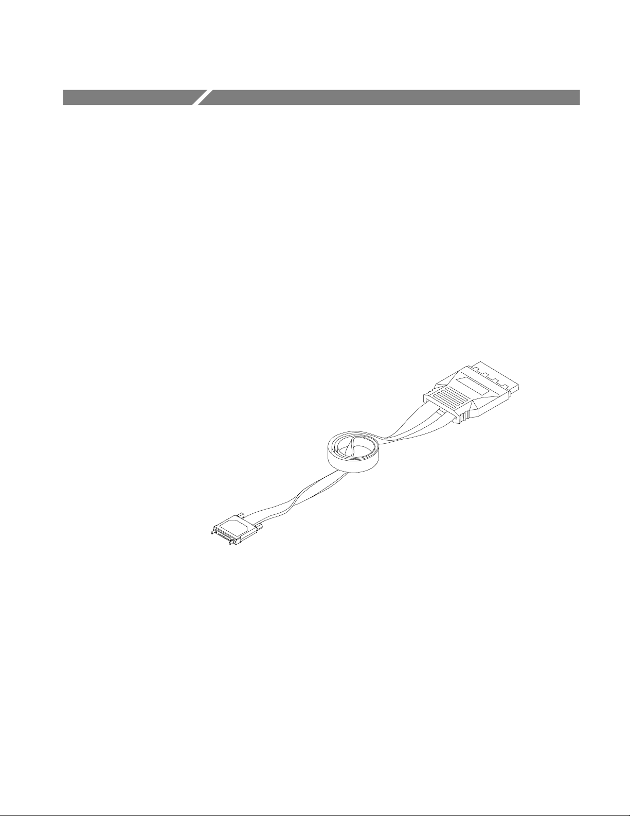
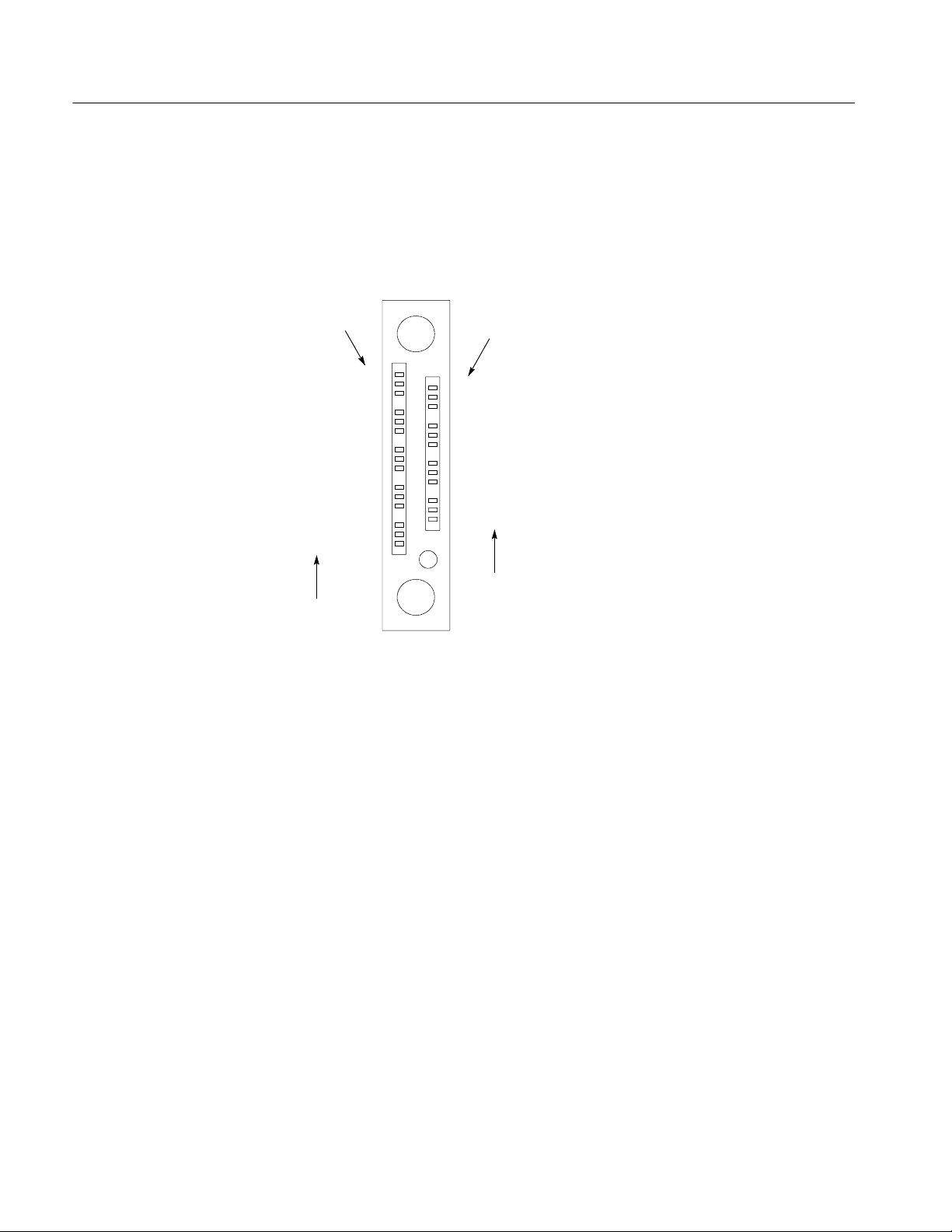
target system. The P6419 Probe is a high-density probe (see Figure 1) consisting
of a single independent probe head of 17 channel connectors each (16 data and
1 clock/qual).
Figure 1: P6419 logic analyzer probe
The following list details the capabilities and qualities of the P6419 Probe:
H Single-ended clock and qualification inputs
H Single-ended data inputs
H Compression contact (eliminates need for built-in connector)
H Land pattern (supports direct signal pass-through)
H Supports PCB thickness of 1.27 mm to 6.35 mm (0.050 in to 0.258 in)
P6419 Logic Analyzer Probe Instructions
1
Page 14
Operating Basics
H Narrow 17-channel probe head (for easier placement and layout)
H 2X mode (for example, 1:2 demultiplexing) uses single-probe head
H Approximately 20% less channel density than current Mictor connectors
H Color-coded keyed signal connectors
H Adapter supports Mictor-based connections
H --3.5 V to +6.5 V input operating range
H --2.0 V to +4.5 V threshold range
H 500 mV minimum single-ended signal amplitude
H Minimal loading of < 0.7 pF @ 20 kΩ to ground loading
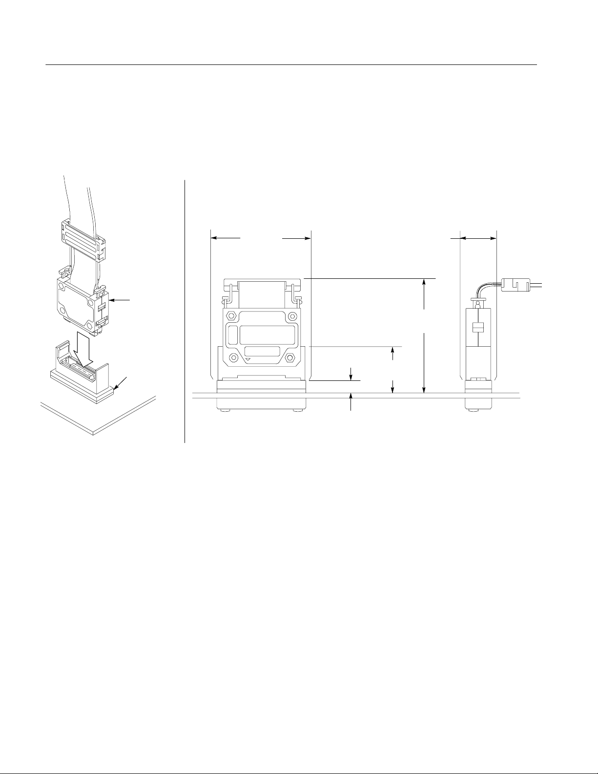
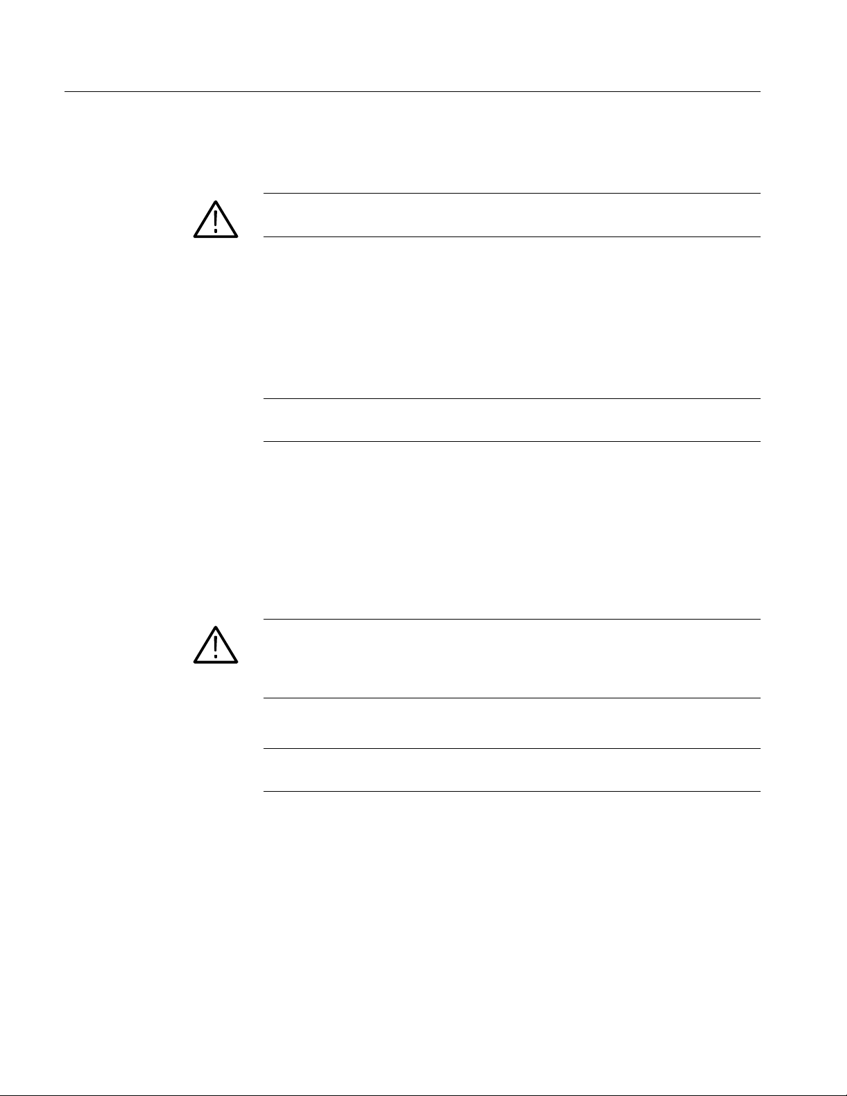
Mictor-on-PCB to
Compression Adapter
Compression
adapter
Mictor adapter
The Mictor-on-PCB to Compression adapter (see Figure NO TAG) allows
existing microprocessor support packages and your hardware designs with
embedded Mictor connectors to be connected to the P6419 High-Density Probe.
32.20 mm
(1.268 in)
58.57 mm
(2.306 in)
20.17 mm
(0.794 in)
Figure 2: Mictor-on-PCB to Compression adapter
2
12.83 mm
(0.505 in)
P6419 Logic Analyzer Probe Instructions
Page 15
Operating Basics
This adapter supports standard Mictor connector footprints and signal connections on older logic analyzer designs.
The Mictor adapter adds 2.7 pF to the high-density compression probe load of
0.7 pF for a combined adapter and probe capacitance load of 3.4 pF.
See Figure 4 on page 4 for comparing the clearances between the P6434 and
compression probe adapters.
Compression-on-PCB to
P6434 Mictor Adapter
Mictor
adapter
Elastomer
holder
Circuit board
The Compression-on-PCB to P6434 Mictor adapter (see Figure 3) allows the
TLA520x mainframe, the TLA6xx mainframe, and TLA7Lx/Mx/Nx/Px/Qx logic
analyzer modules using a P6434 Probe to take advantage of the new compression
footprint and eliminate the need for Mictor connectors in your target system.
NOTE. To use the P6434 adapter, do not install press-in nuts. However, if board
thickness is > .093 in, you will need to install press-in nuts before migrating to
P6419 probes.
Two different screw lengths are required to accommodate the
1.27 mm to 6.35 mm (0.050 in to 0.250 in) PCB thickness range.
This adapter requires the use of the Compression-on-PCB to P6434 Mictor
adapter land footprint. See Figure 15 on page 33 for further information.
The Compression-on--PCB to Mictor adapter adds 1.5 pF to the P6434 probe
load of 2.0 pF for a combined adapter and probe capacitance load of 3.5 pF.
32.131 mm
(1.265 in)
15.82 mm
(0.623 in)
13.716 mm
(0.540 in)
PCB Thickness
1.27 mm to 6.35 mm
(0.050 in to 0.250 in)
Adapter
backing plate
Figure 3: Compression-on-PCB to P6434 Mictor adapter
P6419 Logic Analyzer Probe Instructions
4.572 mm
(0.180 in)
3
Page 16
Operating Basics
To compare the clearance between the P6434 Probe connection and the P6434
Probe connection via the Compression-on-PCB to P6434 Mictor adapter, refer to
Figure 4. Note that the mictor adapter adds 0.145 inches to the height of the
P6434 probe.
P6434
Mictor adapter
32.131 mm
(1.265 in)
15.82 mm
(0.623 in)
3.68 mm
(0.145 in)
13.716 mm
(0.540 in)
34.93 mm
(1.375 in)
Figure 4: Clearance for probe connection using Compression-on-PCB to P6434 Mictor adapter
4
P6419 Logic Analyzer Probe Instructions
Page 17
Operating Basics
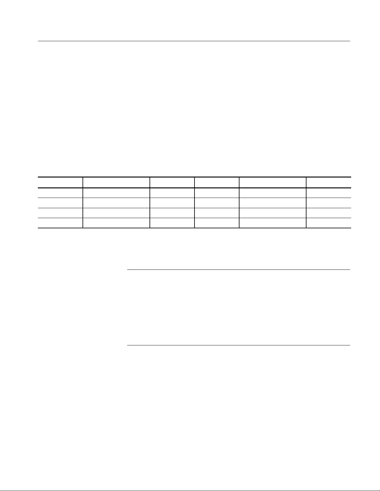
Attaching Probe Labels
When you purchase one or more P6419 logic analyzer probes with a TLA520x
logic analyzer mainframe or TLA7Nx/Px/Qx logic analyzer module, all labels
are already attached. If you purchase the probe seperately from the logic
analyzer, you must apply the color-coded labels as described in this section. The
labels help you identify the probe connections at the logic analyzer end and at
the target system end.
Table 1 lists the probe section and label color combinations. Refer to Table 1 and
to Figure 5 when you attach the probe labels.
Table 1: Probe section and label combinations
Probe section Channels Label color Probe section Channels Label color
A3-A2 CK0, A3:7--0, A2:7-0 Brown A1-A0 CK1, A1:7-0, A0:7-0 Orange
D3-D2 QUAL0, D3:7-0, D2:7-0 Blue D1-D0 CK2, D1:7-0, D0:7-0 Yellow
C3-C2 CK3, C3:7-0, C2:7-0 White C1-C0 QUAL1, C1:7-0, C0:7-0 Gray
E3-E2 QUAL3, E3:7-0, E2:7-0 Green E1-E0 QUAL2, E1:7-0, E0:7-0 Violet
P6419 Labels
Use the following instructions to attach probe labels to your Tektronix P 6419
Logic Analyzer Probe.
NOTE. Always use flat-nosed tweezers to remove the labels from the sheet of
labels. Never peel labels with your fingers. The labels ar e made of soft vinyl and
can stretch and distort easily. To avoid stretching the label, always grasp it from
the top right corner while removing it from the sheet of labels.
The adhesive on the vinyl labels is extremely strong. Carefully align each label
to the intended outline on the module end and probe head before attaching it to
the probe. Once labels are placed on the probe, they become very difficult to
remove.
You will be attaching labels to the module and and both sides of the probe head.
Refer to Figure 5 and use the following steps to attach the probe labels:
1. Identify the module end of the probe cable.
2. From the sheet of labels, locate the color-coded label for the module end of
the probe cable.
3. Attach the matching colored labels to the probe head on the other end of the
probe cable.
P6419 Logic Analyzer Probe Instructions
5
Page 18
Operating Basics
Module end
Probe head
Figure 5: Attaching labels to the P6419 probe
6
P6419 Logic Analyzer Probe Instructions
Page 19
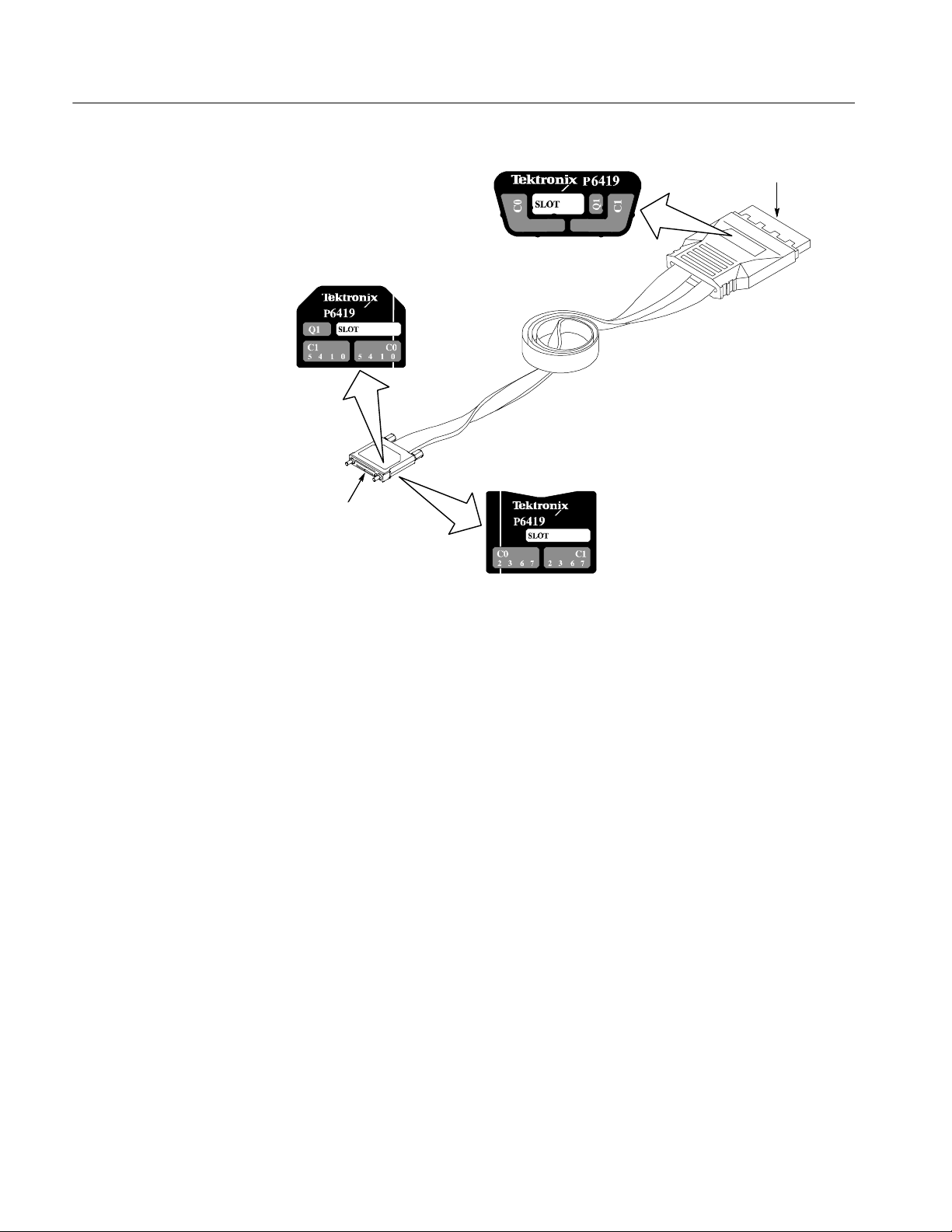
Connecting the Probes to the Logic Analyzer
Connect the logic analyzer probes and the optional retaining brackets as shown
in Figure 6. The retaining brackets and hardware ship with the logic analyzer.
Match color-coded
labels
P6419
Operating Basics
Attach optional probe
retainer brackets
Figure 6: Connecting the probes to the logic analyzer
Refer to Figure 10 and connect the probe to the target system. You can connect
the probes to the target system without turning off the target system.
P6419 Logic Analyzer Probe Instructions
7
Page 20
Operating Basics
Cleaning the P6419 Compression Footprints
CAUTION. To avoid electrical damage, always turn off the power of your target
system before cleaning the compression footprint.
Before connecting the probe to the target system, you must clean the compression footprints on your board according to the following steps:
1. Use a lint-free cloth moistened with isopropyl alcohol and gently wipe the
footprint surface.
2. Remove any remaining lint using a nitrogen air gun.
NOTE. Use alcohol sparingly and be sure that you have removed any remaining
lint or residue with a nitrogen air gun.
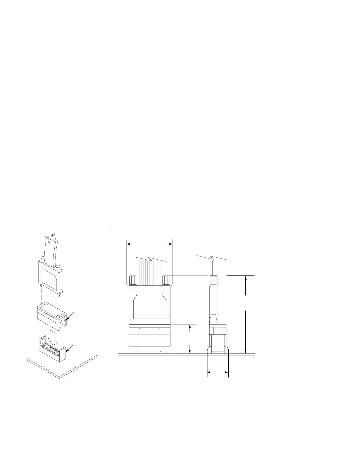
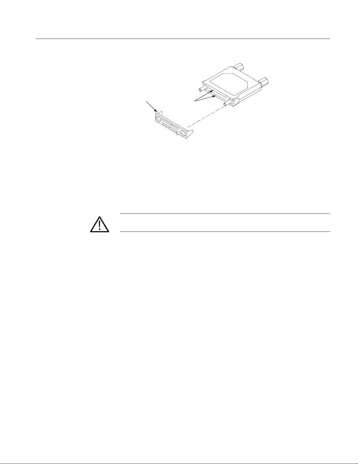
Cleaning the P6419 Probe Heads
Before connecting P6419 probes to the target system, ensure that the probe heads
are free from dust, dirt, and contaminants. If necessary, clean the probe heads
according to the following steps.
CAUTION. Static discharge can damage semiconductor components in the probe
head. Always wear a grounded antistatic wrist strap whenever handling the
probe head. Also verify that the probe head is not connected to anything that
carries a static charge.
NOTE. Never clean the elastomers. Always replace them instead. Refer to the
Replaceable Parts section of this manual for information on ordering parts.
To clean probe heads:
1. Remove elastomer holder.
2. Moisten a cotton swab with isopropyl alcohol.
8
P6419 Logic Analyzer Probe Instructions
Page 21
Operating Basics
Elastomer holder
Figure 7: Cleaning the probe heads
3. Gently wipe the edge print pads of the circuit board.
4. Remove any remaining lint using a nitrogen air gun.
5. Put the elastomer holder back in place.
CAUTION. To avoid damaging the probe contacts, do not touch the elastomer. In
addition, do not reverse the elastomer because this will transfer contaminants.
Storing the P6419 Probe Heads
Print pads
To protect the elastomer, it is important to properly store the probe heads when
the probes are not in use. While holding the probe end at a perpendicular angle to
the nut bar, loosely attach both probe head screws. For further details, see
Figure 8.
P6419 Logic Analyzer Probe Instructions
9
Page 22
Operating Basics
Safely store the
probe head
Nut bar
Nut bar
Figure 8: Storing the probe heads
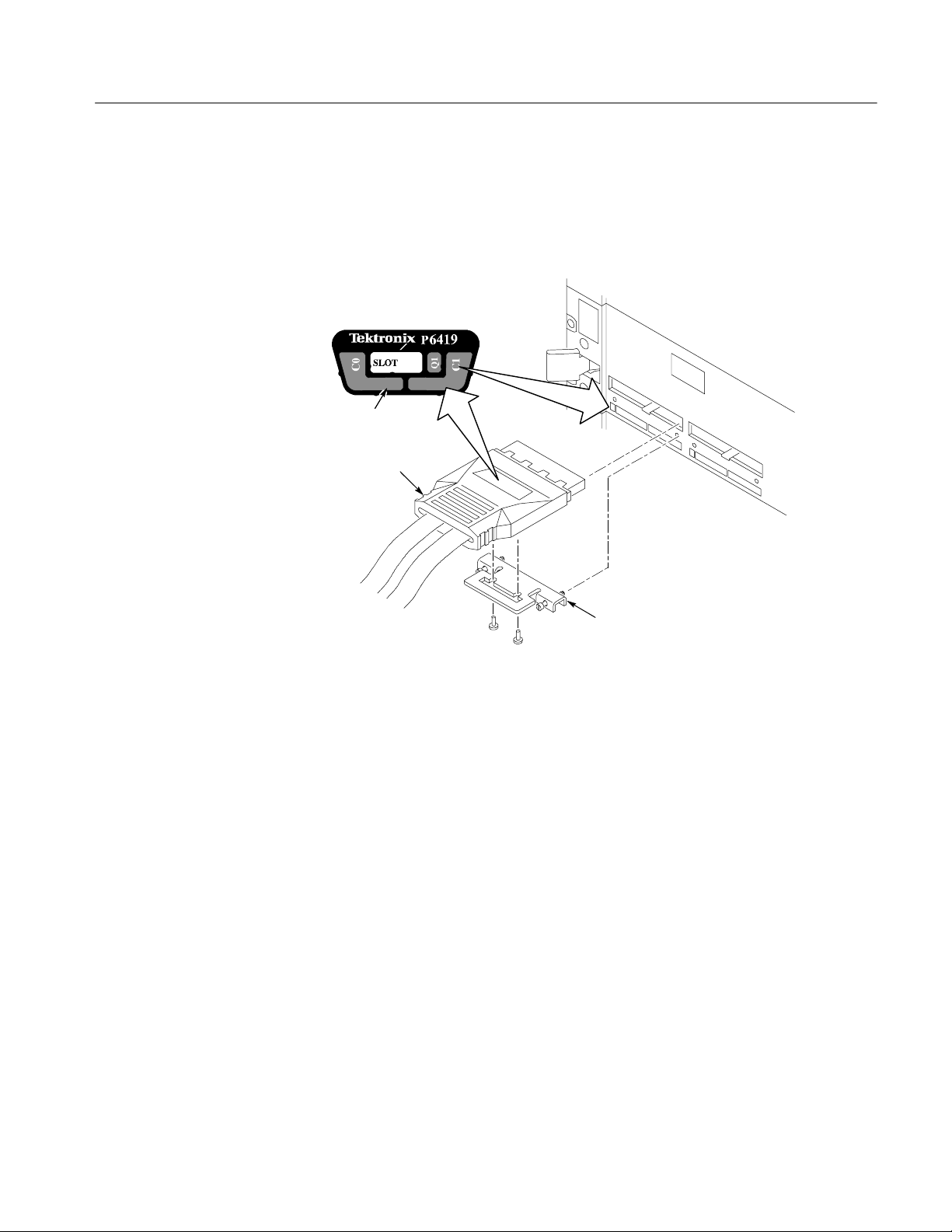
Connecting the Probes to the Target System
Connecting the P6419
High Density Probes
Connect the P6419 High-Density Probes (see Figure 10 on page 12) to the target
system. You can connect the probes to the target system without turning off the
power to the target system.
Installing the Correct Elastomer Holder. If the PCB is ≤.093 in, use the thin
elastomer holder with a nut bar. If the PCB is > .093, use the thick elastomer
holder with a press-in nut.
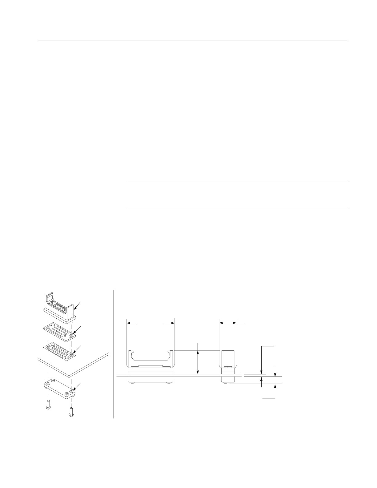
1. Nut Bar.
a. Press the nut bar backing plate into the two holes on the underside of the
compression footprint on the PCB.
b. Locate the keying pin on the probe end and align it to the keying pin
hole on the PCB.
c. While holding the probe end at a perpendicular angle to the PCB,
finger-tighten both probe head screws until snug, not to exceed 1 in-lbs.
You are encouraged to use a torque wrench to ensure proper tightness of
the probe head screws.
10
P6419 Logic Analyzer Probe Instructions
Page 23
Operating Basics
CAUTION. When attaching the probe head to the target system, you must use care
to evenly tighten probe head screws until they are snug. First tighten both screws
until the nut bar makes contact with the board surface, then snug each screw to 1
in-lbs (max). Under-tightening the probe head screws can result in intermittence.
Over-tightening can damage the elastomer holder and strip the screws.
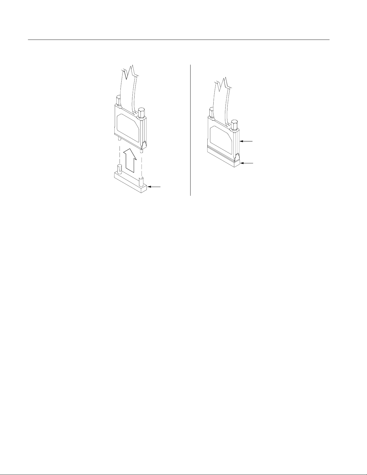
2. Press-in Nut.
a. Install the press-in nuts on the PCB by following the Manufacturer’s
installation procedure. Refer to Figure 9 for press-in nut installation
details.
Keying pin hole
Press--in nuts thread
type (2--56 UNC-2B)
Circuit board
Min 2.362 mm
to Max 6.35 mm
(0.093 in to
0.250 in)
Figure 9: Press-in Nuts installation
b. Locate the keying pin on the probe end and align it to the keying pin
hole on the PCB.
CAUTION. When attaching the probe head to the target system, you must use care
to evenly tighten probe head screws until they are snug. First slightly tighten
both screws, then snug each screw to 1 in-lbs (max). Under-tightening the probe
head screws can result in intermittence. Over-tightening can damage the
elastomer holder and strip the screws.
c. While holding the probe end at a perpendicular angle to the PC B, finger
P6419 Logic Analyzer Probe Instructions
tighten both probe head screws until snug, not to exceed 1 in-lbs. You
are encouraged to use a torque wrench to ensure proper tightness of the
probe head screws.
11
Page 24
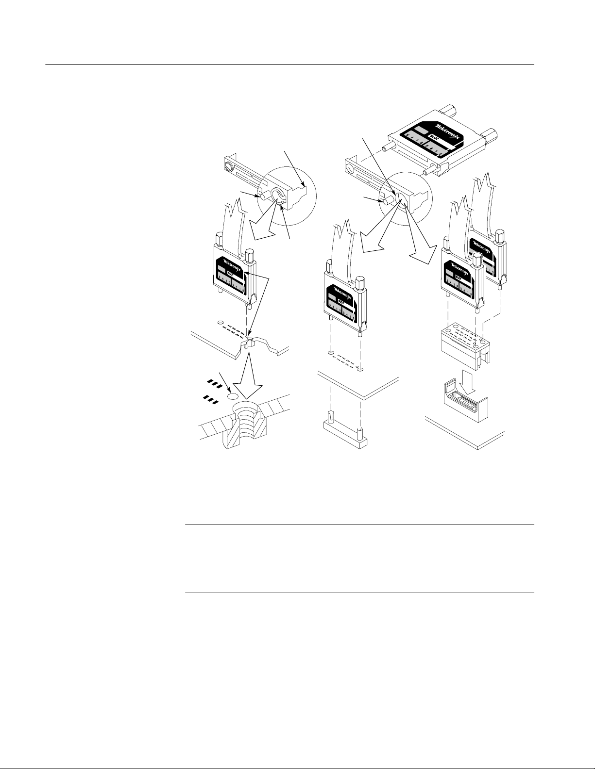
Operating Basics
Note that elastomer
holder is keyed
Thin black,
(no rib)
Keying pin
Keying pin hole
Press--in nuts
Thick gray,
(rib)
White thin line
is keying pin
Keying pin
Nut bar
Mictor--on--PCB
12
Figure 10: Connecting the P6419 probe to the target system
NOTE. The Mictor-on-PCB adapter is labeled with J1 and J2 signal identifiers to
assist you with correctly locating each probe head on the adapter. Each probe
head label contains channel information that you compare with information
contained in the Signal Name column of Table 7 on page 23 to determine the
signal to which you connect the probe head.
P6419 Logic Analyzer Probe Instructions
Page 25

Operating Basics
Connecting the
Mictor-on-PCB to
Compression Adapter
The Mictor-on-PCB to compression adapter allows existing applications of older
logic analyzer modules and probes to connect to the compression footprint. You
can connect the adapter to the target system without turning off the target system.
Connect the adapter according to the following steps:
NOTE. Be sure to use a thin elastomer holder. The thin elastomer is black and
does not have the protruding rib (see Figure 10).
1. While holding the first probe end at a perpendicular angle to the adapter,
place the probe end into the adapter and finger-tighten the screws until snug,
not to exceed 1 in-lbs.
2. Connect the second probe end to the adapter in the same manner.
3. Press the connected probe ends and adapter into the existing Mictor
connector on the PCB.
This adapter supports standard Mictor connector footprints and signal connections on older logic analyzer designs.
The Mictor adapter adds 2.7 pF to the high-density compression probe load of
0.7 pF for a combined adapter and probe capacitance load of 3.4 pF.
Connecting the
Compression-on-PCB to
P6434 Mictor Adapter
The Compression-on-PCB to P6434 Mictor adapter (see Figure 3 on page 3)
allows you to connect the compression footprint to the Mictor connector pins
used by the P6434 Probe. You can connect the adapter to the target system
without turning off the target system. Connect the adapter according to the
following steps:
NOTE. To use this adapter, do not install press-in nuts. However if board
thickness is >.093 in, you will need to install press-in nuts before migrating to
P6419 probes.
1. Place the adapter at a perpendicular angle on top of the compression
footprint.
2. Place the backing plate on the underside of the PCB.
3. Connect the backing plate by sliding the two screws into the existing screw
holes from the underside of the PCB and finger-tighten the screws until
snug, not to exceed 1 in-lbs (typically, 1/2 in-lbs. You are encouraged to use
a torque wrench to ensure proper tightness of probe head screws.
P6419 Logic Analyzer Probe Instructions
13
Page 26

Operating Basics
CAUTION. When attaching the probe head to the target system, you must use care
to evenly tighten probe head screws until they are snug. First slightly tighten
both screws, then snug each screw to 1 in-lbs (max). Under-tightening the probe
head screws can result in intermittence. Over-tightening can damage the
elastomer holder and strip the screws.
4. Plug the P6434 Probe into the adapter.
Screws of two different lengths are provided to attach the adapter to your PCB.
The length of screw you need depends on the thickness of the P CB (0.050 in to
0.250 in).
This adapter requires use of the Compression-on-PCB to P6434 Mictor adapter
land footprint. For further dimensional information, refer to the Compression-onPCB to P6434 Mictor adapter land footprint (see Figure 15 on page 33).
14
P6419 Logic Analyzer Probe Instructions
Page 27

Reference
This section provides reference information and specifications for the P6419
high-density probe. Topics include the following:
H Designing an interface between the probe and a target system
H Specifications
Designing an Interface Between the P6419 Probe and a Target System
Once you have determined which probe is required, use the following information to design the appropriate connector into your target system board. The
following topics are in this section:
H Signal fixturing considerations
H Signal connections (signal names and land footprint)
H Mechanical considerations
H Electrical considerations
Signal Fixturing
Considerations
This section contains the following information to consider for signal fixturing:
H Clocks and qualifiers
H Merged modules and source synchronous clocking
H Demultiplexing multiplexed buses
H 2X high resolution timing modes (Internal 2X)
H 4X high resolution timing modes (Internal 4X -- TLA520x logic analyzer
mainframes only)
H Range recognition
Clocks and Qualifiers. Every logic analyzer has some special purpose input
channels. Inputs designated as clocks can cause the analyzer to store data.
Qualifier channels can be logically AND’ed and OR’ed with clocks to further
define when the analyzer should latch data from the system under test. Routing
the appropriate signals from our design to these inputs will ensure that the
analyzer can acquire data correctly.
P6419 Logic Analyzer Probe Instructions
15
Page 28

Reference
Depending on the channel width, each TLA520x mainframe, TLA6xx mainframe, and TLA7Lx/Mx/Nx/Px/Qx module will have a different set of clock and
qualifier channels. Table 2 shows the clock and qualifier channels available for
each instrument.
Table 2: Logic analyzer clock and qualifier availability
Clock Inputs Qualifier Inputs
TLA Mainframe
TLA5201
TLA7L1/M1/N1
TLA601/11/21
TLA5202
TLA7L2/M2/N2/P2/Q2
TLA602/12/22
TLA5203
TLA7L3/M3/N3
TLA602/13/23
TLA5204
TLA7L4/M4/N4/P4/Q4
TLA604/14/24
CLK:0
n n
n n n n
n n n n n n
n n n n n n n n
CLK:1 CLK:2 CLK:3 QUAL:0 QUAL:1 QUAL:2 QUAL:3
All clock and qualifier channels are stored. The analyzer stores the logic state of
these channels every time it latches data.
Since clock and qualifier channels are stored in the logic analyzer’smemory,
there is no need to double probe these signals for timing analysis. When
switching from state to timing analysis modes, all of the clock and qualifier
signals are visible. This also allows you to route regular signals, those not
needed for clocking, to these channels when they are not being used for their
special purpose.
16
It is good practice to take advantage of these channels to increase your options
for when you will latch data. Routing several of your design’s clocks and strobes
to the logic analyzer clock inputs provides you with greater flexibility in the
logic analyzer clocking setup menus.
As an example, look at a microprocessor with a master clock, data strobe, and an
address strobe. Routing all three of these signals to analyze clock inputs enables
you to latch data on the processor master clock, only when data is strobes or only
when address is strobed. Some forethought in signal routing can greatly expand
the ways in which you can latch and analyze data.
P6419 Logic Analyzer Probe Instructions
Page 29
Reference
A microprocessor also provides a good example of signals that can be useful as
qualifiers. There are often signals that indicate data reads versus data writes
(R/W), signals that show when alternate bus masters have control of the
processor buses (DMA), and signals that show when various memory devices are
being used (ChipSel). All of these signals are good candidates for assignment to
qualifier channels.
By logically AND’ing the clock with one of these qualifiers, you can program
the analyzer to store only data reads or data writes. Using the DMA signal as a
qualifier provides a means of filtering out alternate bus master cycles. Chip
selects can limit data latching to specific memory banks, I/O ports, or peripheral
devices.
Demultiplexing Multiplexed Buses. TLA7Nx/Px/Qx modules and TLA6xx
mainframes support 2X demultiplexing. However, only TLA520x mainframes
support 4X demultiplexing. Each signal on a dual multiplexed bus can be
demultiplexed into its own logic analyzer channel. See Table 3 and Table 4 to
determine which channel groups to connect to feed channels in the target system
the test data.
Table 3: 2X Demultiplexing source-to-destination channel assignments
Source
connecting channel
groups
A3:7--0 D3:7--0 D3:7--0 C3:7--0 C3:7--0
A2:7--0 D2:7--0 D2:7--0 C2:7--0 C2:7--0
A1:7--0 D1:7--0 D1:7--0 D1:7--0
A0:7--0 D0:7--0 D0:7--0 D0:7--0
C3:7--0 C1:7--0 C1:7--0
C2:7--0 C0:7--0 C0:7--0
E3:7--0 E1:7--0
E2:7--0 E0:7--0
CLK:0 QUAL:1 QUAL:1
CLK:1 QUAL:0 QUAL:0
CLK:2 QUAL:3
CLK:3 QUAL:2
Destination channels receiving target system test data
TLA5204
TLA7N4/P4/Q4
TLA604/14/24
TLA5203
TLA7LN3
TLA602/13/23
TLA5202
TLA7LN2/P2/Q2
TLA602/12/22
TLA5201
TLA7N1
TLA601/11/21
P6419 Logic Analyzer Probe Instructions
17
Page 30

Reference
Table 4: 4X Demultiplexing source-to-destination channel assignments
Source
connecting channel
groups
C3:7--0 C2:7--0
A1:7--0 A0:7--0
A3:7--0 A2:7--0
E3:7--0 E2:7--0
CLK:3 CLK:2
CLK:1 CLK:0
Destination channels receiving target system test data
TLA5201
C1:7--0
C0:7--0
D1:7--0
D0:7--0
D3:7--0
D2:7--0
E1:7--0
E0:7--0
QUAL:3
QUAL:2
QUAL:1
QUAL:0
TLA5202 TLA5203 TLA5204
C2:7--0
C1:7--0
C0:7--0
A0:7--0
D1:7--0
D0:7--0
A2:7--0
D3:7--0
D2:7--0
CLK:0
QUAL:1
QUAL:0
A3:7--0
A2:7--0
C2:7--0
A0:7--0
D1:7--0
D0:7--0
A3:7--0
A2:7--0
C2:7--0
When demultiplexing data, there is no need to connect the destination channels
to the multiplexed bus. Data from the source channels are routed to the destination channels internal to the logic analyzer. Table 3 and Table 4 show the
mapping of source channels to destination channels.
18
Demultiplexing affects only the main memory for the destination channels. This
means that the MagniVu memory is filled with data from whatever is connected
to the demultiplexing destination channel probe inputs. This provides an
opportunity to acquire high resolution MagniVu data on a few extra channels.
Connecting the demultiplexing destination channels to other signals will allow
viewing of their activity in the MagniVu memory but not the main memory.
2X and 4X High Resolution Timing Modes. 2X high resolution timing mode
provides double the normal 500 MHz sample rate on one-half of the channels.
By trading half of the analyzers channels, the remaining channels can be sampled
at a 1 GHz rate with double the memory depth. 4X high resolution timing mode
provides quadruple the normal 500 MHz sample rate on one-fourth of the
channels. By trading three-fourths of the analyzer’s channels, the remaining
channels can be sampled at 2 GHz with quadruple the memory depth.
P6419 Logic Analyzer Probe Instructions
Page 31

Reference
Both of the high resolution timing modes use the same demultiplexing channel
routing as shown in Tables 3 and 4. By taking care to assign critical signals to
the demultiplexing source channels, you can obtain extra timing resolution where
most needed. Since demultiplexing affects only the main memory, you will still
have the MagniVu data available for all of the signals that are disconnected from
the main memory when you switch to the high resolution timing modes.
Range Recognition. When using range recognizers, the probe groups and probe
channels must be in hardware order. Probe groups must be used from the
most-significant probe group to the least-significant probe group based on the
following order:
C3 C2 C1 C0 E3 E2 E1 E0 A3 A2 D3 D2 A1 A0 D1 D0 Q3 Q2 Q1 Q0 CK3
CK2 CK1 CK0
Probe channels must be from the most-significant channel to the least-significant
channel, based on the following order:
76543210
Signal Names
The above examples apply to a 136-channel logic analyzer module. The missing
channels in LA modules with fewer than 136 channels are ignored. With merged
modules, range recognition extends across the first three modules: the master
module contains the most-significant channels.
See Tables 5 through 8 for the P6419 probe and adapter signal connections.
P6419 Logic Analyzer Probe Instructions
19
Page 32

Reference
Table 5: P6419 High-Density Probe channel mapping on 136 and 102 channel TLA7Lx/Mx/Nx/Px/Qx modules and
both TLA6xx and TLA520x mainframes
Signal
name
Clk/Qual-- NC NC NC NC NC NC NC NC NC
GND A14 GND GND GND GND GND GND GND GND
Clk/Qual+ A13 Q3+ Q2+ CK0+ Q0+ CK1+ CK2+ CK3+ Q1+
Data 15 B12 E3:7 E1:7 A3:7 D3:7 A1:7 D1:7 C3:7 C1:7
GND B11 GND GND GND GND GND GND GND GND
Data 14 B10 E3:6 E1:6 A3:6 D3:6 A1:6 D1:6 C3:6 C1:6
Data 13 A12 E3:5 E1:5 A3:5 D3:5 A1:5 D1:5 C3:5 C1:5
GND A11 GND GND GND GND GND GND GND GND
Data 12 A10 E3:4 E1:4 A3:4 D3:4 A1:4 D1:4 C3:4 C1:4
Data 11 B9 E3:3 E1:3 A3:3 D3:3 A1:3 D1:3 C3:3 C1:3
GND B8 GND GND GND GND GND GND GND GND
Data 10 B7 E3:2 E1:2 A3:2 D3:2 A1:2 D1:2 C3:2 C1:2
Data 9 A9 E3:1 E1:1 A3:1 D3:1 A1:1 D1:1 C3:1 C1:1
GND A8 GND GND GND GND GND GND GND GND
Data 8 A7 E3:0 E1:0 A3:0 D3:0 A1:0 D1:0 C3:0 C1:0
Data 7 B6 E2:7 E0:7 A2:7 D2:7 A0:7 D0:7 C2:7 C0:7
GND B5 GND GND GND GND GND GND GND GND
Data 6 B4 E2:6 E0:6 A2:6 D2:6 A0:6 D0:6 C2:6 C0:6
Data 5 A6 E2:5 E0:5 A2:5 D2:5 A0:5 D0:5 C2:5 C0:5
GND A5 GND GND GND GND GND GND GND GND
Data 4 A4 E2:4 E0:4 A2:4 D2:4 A0:4 D0:4 C2:4 C0:4
Data 3 B3 E2:3 E0:3 A2:3 D2:3 A0:3 D0:3 C2:3 C0:3
GND B2 GND GND GND GND GND GND GND GND
Data 2 B1 E2:2 E0:2 A2:2 D2:2 A0:2 D0:2 C2:2 C0:2
Data 1 A3 E2:1 E0:1 A2:1 D2:1 A0:1 D0:1 C2:1 C0:1
GND A2 GND GND GND GND GND GND GND GND
Data 0 A1 E2:0 E0:0 A2:0 D2:0 A0:0 D0:0 C2:0 C0:0
Refer to Table 3 on page 17 for 2X demultiplexing channel assignments.
Pad
name
Probe Q3,
E3, E2
Probe Q2,
E1, E0
Probe
CK0, D3,
D2
Probe Q0,
D3, D2
Probe
CK1, A1,
A0
Probe
CK2, D1,
D0
Probe
CK3, C3,
C2
Probe Q1,
C1, C0
20
P6419 Logic Analyzer Probe Instructions
Page 33
Reference
Table 6: Recommended Compression-on-PCB to P6434 Mictor adapter and Mictor-on-PCB to Compression adapter
channel mapping for 136 and 102 channel modules
136 channel module
102 channel module
Signal name Pad name
Mictor pin number
J1 Clk/Qual-- A15 NC NC NC NC NC
GND A14 GND GND GND GND GND
J1 Clk/Qual+ A13 5 Q3 Q0 CK0 CK3
J1 Data 15 B12 7 E3:7 D3:7 A3:7 C3:7
GND B11 GND GND GND GND GND
J1 Data 14 B10 9 E3:6 D3:6 A3:6 C3:6
J1 Data 13 A12 11 E3:5 D3:5 A3:5 C3:5
GND A11 GND GND GND GND GND
J1 Data 12 A10 13 E3:4 D3:4 A3:4 C3:4
J1 Data 11 B9 15 E3:3 D3:3 A3:3 C3:3
GND B8 GND GND GND GND GND
J1 Data 10 B7 17 E3:2 D3:2 A3:2 C3:2
J1 Data 9 A9 19 E3:1 D3:1 A3:1 C3:1
GND A8 GND GND GND GND GND
J1 Data 8 A7 21 E3:0 D3:0 A3:0 C3:0
J1 Data 7 B6 23 E2:7 D2:7 A2:7 C2:7
GND B5 GND GND GND GND GND
J1 Data 6 B4 25 E2:6 D2:6 A2:6 C2:6
J1 Data 5 A6 27 E2:5 D2:5 A2:5 C2:5
GND A5 GND GND GND GND GND
J1 Data 4 A4 29 E2:4 D2:4 A2:4 C2:4
J1 Data 3 B3 31 E2:3 D2:3 A2:3 C2:3
GND B2 GND GND GND GND GND
J1 Data 2 B1 33 E2:2 D2:2 A2:2 C2:2
J1 Data 1 A3 35 E2:1 D2:1 A2:1 C2:1
GND A2 GND GND GND GND GND
J1 Data 0 A1 37 E2:0 D2:0 A2:0 C2:0
Adapter #4/
probe head #4
Adapter #3/
probe head #3
Adapter #2/
probe head #2
Adapter #1/
probe head #1
P6419 Logic Analyzer Probe Instructions
21
Page 34
Reference
Table 6: Recommended Compression-on-PCB to P6434 Mictor adapter and Mictor-on-PCB to Compression adapter
channel mapping for 136 and 102 channel modules (Cont.)
136 channel module
102 channel module
Signal name Adapter #1/
J2 Clk/Qual-- A15 NC NC NC NC NC
GND A14 GND GND GND GND GND
J2 Clk/Qual+ A13 6 Q2 CK2 CK1 Q1
J2 Data 15 B12 8 E1:7 D1:7 A1:7 C1:7
GND B11 GND GND GND GND GND
J2 Data 14 B10 10 E1:6 D1:6 A1:6 C1:6
J2 Data 13 A12 12 E1:5 D1:5 A1:5 C1:5
GND A11 GND GND GND GND GND
J2 Data 12 A10 14 E1:4 D1:4 A1:4 C1:4
J2 Data 11 B9 16 E1:3 D1:3 A1:3 C1:3
GND B8 GND GND GND GND GND
J2 Data 10 B7 18 E1:2 D1:2 A1:2 C1:2
J2 Data 9 A9 20 E1:1 D1:1 A1:1 C1:1
GND A8 GND GND GND GND GND
J2 Data 8 A7 22 E1:0 D1:0 A1:0 C1:0
J2 Data 7 B6 24 E0:7 D0:7 A0:7 C0:7
GND B5 GND GND GND GND GND
J2 Data 6 B4 26 E0:6 D0:6 A0:6 C0:6
J2 Data 5 A6 28 E0:5 D0:5 A0:5 C0:5
GND A5 GND GND GND GND GND
J2 Data 4 A4 30 E0:4 D0:4 A0:4 C0:4
J2 Data 3 B3 32 E0:3 D0:3 A0:3 C0:3
GND B2 GND GND GND GND GND
J2 Data 2 B1 34 E0:2 D0:2 A0:2 C0:2
J2 Data 1 A3 36 E0:1 D0:1 A0:1 C0:1
GND A2 GND GND GND GND GND
J2 Data 0 A1 38 E0:0 D0:0 A0:0 C0:0
Refer to Table 3 on page 17 for 2X demultiplexing channel assignments.
Pad name
Mictor pin number
Adapter #4/
probe head #4
Adapter #3/
probe head #3
Adapter #2/
probe head #2
probe head #1
Any differential input, either the differential clock/qualifiers or the P6419 high-density probe, may have its negative input
pin grounded and be used as a single-ended input.
22
P6419 Logic Analyzer Probe Instructions
Page 35
Reference
Table 7: Recommended Compression-on-PCB to P6434 Mictor adapter and Mictor-on-PCB to Compression adapter
channel mapping for 68 channel module
Signal name Pad name Mictor pin num ber Adapter #1/
probe head #1
J1 Clk/Qual-- A15 NC NC NC
GND A14 GND GND GND
J1 Clk/Qual+ A13 5 CK0 CK3
J1 Data 15 B12 7 A3:7 C3:7
GND B11 GND GND GND
J1 Data 14 B10 9 A3:6 C3:6
J1 Data 13 A12 11 A3:5 C3:5
GND A11 GND GND GND
J1 Data 12 A10 13 A3:4 C3:4
J1 Data 11 B9 15 A3:3 C3:3
GND B8 GND GND GND
J1 Data 10 B7 17 A3:2 C3:2
J1 Data 9 A9 19 A3:1 C3:1
GND A8 GND GND GND
J1 Data 8 A7 21 A3:0 C3:0
J1 Data 7 B6 23 A2:7 C2:7
GND B5 GND GND GND
J1 Data 6 B4 25 A2:6 C2:6
J1 Data 5 A6 27 A2:5 C2:5
GND A5 GND GND GND
J1 Data 4 A4 29 A2:4 C2:4
J1 Data 3 B3 31 A2:3 C2:3
GND B2 GND GND GND
J1 Data 2 B1 33 A2:2 C2:2
J1 Data 1 A3 35 A2:1 C2:1
GND A2 GND GND GND
J1 Data 0 A1 37 A2:0 C2:0
Adapter #2/
probe head #1
P6419 Logic Analyzer Probe Instructions
23
Page 36

Reference
Table 7: Recommended Compression-on-PCB to P6434 Mictor adapter and Mictor-on-PCB to Compression adapter
channel mapping for 68 channel module (Cont.)
Signal name Adapter #2/
J2 Clk/Qual+ A15 NC NC NC
GND A14 GND GND GND
J2 Clk/Qual+ A13 6 CK1 CK2
J2 Data 15 B12 8 A1:7 D1:7
GND B11 GND GND GND
J2 Data 14 B10 10 A1:6 D1:6
J2 Data 13 A12 12 A1:5 D1:5
GND A11 GND GND GND
J2 Data 12 A10 14 A1:4 D1:4
J2 Data 11 B9 16 A1:3 D1:3
GND B8 GND GND GND
J2 Data 10 B7 18 A1:2 D1:2
J2 Data 9 A9 20 A1:1 D1:1
GND A8 GND GND GND
J2 Data 8 A7 22 A1:0 D1:0
J2 Data 7 B6 24 A0:7 D0:7
GND B5 GND GND GND
J2 Data 6 B4 26 A0:6 D0:6
J2 Data 5 A6 28 A0:5 D0:5
GND A5 GND GND GND
J2 Data 4 A4 30 A0:4 D0:4
J2 Data 3 B3 32 A0:3 D0:3
GND B2 GND GND GND
J2 Data 2 B1 34 A0:2 D0:2
J2 Data 1 A3 36 A0:1 D0:1
GND A2 GND GND GND
J2 Data 0 A1 38 A0:0 D0:0
1/2 channel mode may use Adapter #1 connection signals as source.
Mictor pin numberPad name
Adapter #1/
probe head #1
probe head #1
Refer to Table 3 on page 17 for 2X demultiplexing channel assignments.
Any differential input, either the differential clock/qualifiers or the P6419 high-density probe, may have its negative input
pin grounded and be used as a single-ended input.
24
P6419 Logic Analyzer Probe Instructions
Page 37

Reference
Table 8: Recommended Compression-on-PCB to P6434 Mictor adapter and Mictor-on-PCB to Compression adapter
channel mapping for 34 channel module
Signal name Pad name Mictor pin number Adapter #1/probe head #1
J1 Clk/Qual-- A15 NC NC
GND A14 GND GND
J1 Clk/Qual+ A13 5 CK3
J1 Data 15 B12 7 C3:7
GND B11 GND GND
J1 Data 14 B10 9 C3:6
J1 Data 13 A12 11 C3:5
GND A11 GND GND
J1 Data 12 A10 13 C3:4
J1 Data 11 B9 15 C3:3
GND B8 GND GND
J1 Data 10 B7 17 C3:2
J1 Data 9 A9 19 C3:1
GND A8 GND GND
J1 Data 8 A7 21 C3:0
J1 Data 7 B6 23 C2:7
GND B5 GND GND
J1 Data 6 B4 25 C2:6
J1 Data 5 A6 27 C2:5
GND A5 GND GND
J1 Data 4 A4 29 C2:4
J1 Data 3 B3 31 C2:3
GND B2 GND GND
J1 Data 2 B1 33 C2:2
J1 Data 1 A3 35 C2:1
GND A2 GND GND
J1 Data 0 A1 37 C2:0
P6419 Logic Analyzer Probe Instructions
25
Page 38

Reference
Table 8: Recommended Compression-on-PCB to P6434 Mictor adapter and Mictor-on-PCB to Compression adapter
channel mapping for 34 channel module (Cont.)
Signal name Adapter #1/probe head #1Mictor pin numberPad name
J2 Clk/Qual+ A15 NC NC
GND A14 GND GND
J2 Clk/Qual+ A13 6 CK0
J2 Data 15 B12 8 A3:7
GND B11 GND GND
J2 Data 14 B10 10 A3:6
J2 Data 13 A12 12 A3:5
GND A11 GND GND
J2 Data 12 A10 14 A3:4
J2 Data 11 B9 16 A3:3
GND B8 GND GND
J2 Data 10 B7 18 A3:2
J2 Data 9 A9 20 A3:1
GND A8 GND GND
J2 Data 8 A7 22 A3:0
J2 Data 7 B6 24 A2:7
GND B5 GND GND
J2 Data 6 B4 26 A2:6
J2 Data 5 A6 28 A2:5
GND A5 GND GND
J2 Data 4 A4 30 A2:4
J2 Data 3 B3 32 A2:3
GND B2 GND GND
J2 Data 2 B1 34 A2:2
J2 Data 1 A3 36 A2:1
GND A2 GND GND
J2 Data 0 A1 38 A2:0
Refer to Table 3 on page 17 for 2X demultiplexing channel assignments.
Any differential input, either the differential clock/qualifiers or the P6419 high-density probe, may have its negative input
pin grounded and be used as a single-ended input.
26
P6419 Logic Analyzer Probe Instructions
Page 39

Reference
Special Considerations for the Adapters. Consider the following issue when you
use either the Compression-on-PCB to P6434 Mictor adapter or the Mictor-on-PCB to Compression adapters:
H Use of the Compression-on-PCB to P6434 Mictor and Mictor-on-PCB to
Compression adapters on existing 68 and 34 channel embedded configurations and supports may require exchanging the P6419 Probe heads or P6434
module connector ends to accommodate all older Tektronix logic analyzer
signal connection alternatives.
Land Footprints
The following section shows the land footprints for the P6419 probe. The figures
contain the signal to land pattern assignments.
P6419 Logic Analyzer Probe Instructions
27
Page 40
Reference
P6419 Probe Land Footprint. See Figure 11 for the land footprint for the P6419
High-Density Probe. See Figure 12 for an example of the high-density probe
land footprint in a typical pass-through signal path layout configuration. This
type of configuration optimizes minimal probe loading. Figure 13 contains
example layouts of the high-density compression and mictor land footprints.
Pad
name
N/C
GND
CLK+
D13
GND
D12
D9
GND
D8
D5
GND
D4
D1
GND
D0
A15
A14
A13
A12
A11
A10
A9
A8
A7
A6
A5
A4
A3
A2
A1
B12
B11
B10
B9
B8
B7
B6
B5
B4
B3
B2
B1
Pad
name
D15
GND
D14
D11
GND
D10
D7
GND
D6
D3
GND
D2
Signal
Signal
name
name
Probe Head
Figure 11: P6419 High-Density probe land footprint
28
P6419 Logic Analyzer Probe Instructions
Page 41

Reference
Signal Name Pad Name
N/C A15
CLK/Qual+ A13
Data15 B12 GND B11
Data14 B10
Data13 A12 GND A11
Data12 A10
Data11 B9 GND B8
Data10 B7
Data9 A9 GND A8
Data8 A7
Data7 B6 GND B5
Data6 B4
Data5 A6 GND A5
Data4 A4
Data3 B3 GND B2
Data2 B1
Data1 A3 GND A2
Data 0 (LSB) A1
Signal Name Pad Name
GND A14
Figure 12: High-Density probe land footprint in a typical pass-through signal path
layout configuration
Figure 13: Example layout of the High-Density compression compared to the mictor
land footprints
P6419 Logic Analyzer Probe Instructions
29
Page 42

Reference
Mechanical
Considerations
This section provides information on compression land footprint requirements
and physical attachment requirements.
The PCB holes, in general, do not have an impact upon the integrity of your
signals. Signal integrity impact is eliminated when the signals you route around
the holes have the corresponding return current plane immediately below the
signal trace (for the entire signal path from driver to receiver).
NOTE. For optimum signal integrity, there should be a continuous, uninterrupted
ground return plane along the entire signal path.
Land Footprint Requirements for P6419 Probes. See Figure 14 for the compression land footprint requirements for P6419 probes.
30
P6419 Logic Analyzer Probe Instructions
Page 43

32.13 mm
(1.265 in)
Reference
6.25 mm (0.250 in) X 32.13 mm (1.265 in)
Frontside component keepout area
6.35 mm
(0.250 in)
6.25 mm (0.250-in) X 32.13 mm (1.265-in)
backside component keepout area for Nut Bar
version, press-in nut clearance only required
0.25 mm (0.010 in)
4X 1.16 mm (0.046 in)
5X 1.16 mm (0.046 in)
on press--in nut version
3X 0.81 mm (0.032 in)
3X 0.41 mm (0.016 in)
25.65 mm (1.010 in)
22.81 mm (0.898 in)
21.49 mm (0.846 in)
6.50 mm (0.256 in)
3.68 mm (0.145 in)
8.51 mm (0.335 in)
12.17 mm (0.479 in)
15.82 mm (0.623 in)
19.48 mm (0.767 in)
13.49 mm (0.531 in)
9.83 mm (0.387 in)
17.15 mm (0.675 in)
20.80 mm (0.819 in )
6.17 mm (0.243 in)
4.17 mm (0.164 in)
1.70 mm (0.067 in) diameter
2X 3.50 mm (0.138 in) diameter
thin PCB with nut bar
3.18 mm (0.125 in)
1.14 mm (0.045 in)
.000
3.18 mm (0.125 in)
2X 3.73 mm (0.147 in) diameter
thick PCB with press in nut
0.000
3.25 mm (0.128 in)
* 2X 5.72 mm (0.225 in)
diameter external layers
* 2X 4.57 mm (0.180 in)
diameter external layers
0.25 mm (0.010 in)
.000
Position B12
0.91 mm (0.036 in)
All dimensions are per standard IPC
tolerance, which is ᐔ0.004
0.91 mm (0.036 in)
Position A15
Figure 14: Land footprint requirements for P6419 probes (t op view)
P6419 Logic Analyzer Probe Instructions
* The need for additional keepout area depends on
the requirements of both your PCB manufacturer and
your outsourced PCB assembly manufacturer.
Position B1
Via Keepout
White silk--screen bar to indicate
directional keying hole (easier
orientation identification)
Probe body keepout
Position A1
31
Page 44

Reference
Special Considerations
WARNING. To avoid personal injury due to electric shock, always turn off the
power on your target system before cleaning the compression footprint.
H Cleanliness is important for a reliable connection. Refer to Cleaning the
P6419 Compression Footprints, located on page 8.
H Line boxes around the pin groupings are the via keepout areas (not part of
the actual land footprint).
H Solder mask is required between all land pads in the component keepout
area.
H Maintain PCB and solder mask tolerances for all signal runs in the keepout
areas to ensure that no exposed runs or metal exist between pads. This
prevents shorted signal runs.
H Solder mask hardness of at least 8H (pencil hardness) and thickness of at
least 0.0762 mm to 0.1270 mm (0.0003 to 0.0005 in) has been verified for
several hundred cycles without appreciable wear from the compression
contact cycling.
H The compression land footprint design was verified on the immersion gold
process.
Land Footprint Requirements for the Compression-on-PCB to P6434 Mictor
Adapter. See Figure 15 for the land footprint requirements for the Compression-
on-PCB to P6434 Mictor adapter. This compression adapter converts from the
new compression footprint to the existing P6434 Mictor-based 34-channel probe.
Refer to the P6434 Mass Termination Probe Manual for the Mictor land
footprint specification. Refer to Table 6 for the recommended channel mappings
for the Compression-on-PCB to P6434 Mictor adapter and Mictor-on-PCB to
Compression adapter.
32
P6419 Logic Analyzer Probe Instructions
Page 45

32.13 mm
(1.265 in)
Reference
J2
13.72 mm
(0.540 in) Total
Keepout
J1
6.60 mm
(0.260 in)
Figure 15: Land footprint requirements for the Compression-on-PCB to P6434
Mictor adapter
Special Considerations
H Two compression land footprints must be spaced as per the mechanical
dimensions specified to support the compression adapter.
H Placement of the compression land footprints is only constrained with use of
the compression adapter, not in normal usage of the TLA7Nx/Px/Qx logic
analyzer module, the TLA600 series mainframes, or the TLA5000 series
mainframes with a high-density probe.
H The P6434 Probe and older logic analyzer modules do not support differen-
tial signals. Therefore, the compression adapter cannot be used to support
differential signals beyond capturing each side of the differential signal
independently in a single-ended manner. Note that the connection to the
CLK/QUAL signal is only connected to the positive side of the signal.
H The compression adapter will add capacitance to the P6434 probe input
capacitance. The Mictor adapter adds 2.7 pF to the high-density compression
probe load of 0.7 pF for a combined adapter capacitance load of 3.4 pF.
H The TLA7Lx/Mx/Nx/Px/Qx logic analyzer module, TLA600 series
mainframe, and TLA5000 series mainframe with a P6419 High-Density
Probe will connect directly to the compression land footprint to support high
performance data capture and viewing needs.
Physical Attachment Requirements for P6419 probes. The connector-less P6419
High-Density Probe interconnects are designed to accommodate PCB thickness
ranging from 1.27 mm to 6.35 mm (0.050 in to 0.250 in). To accommodate this
range, there are two versions of the design:
H Nut bar
H Press-in nut
P6419 Logic Analyzer Probe Instructions
33
Page 46

Reference
If the PCB thickness is 1.27 mm to 2.36 mm (0.050 in to 0.093 in), use the nut
bar with the thin elastomer (see Figure 16).
If the PCB thickness is 2.36 mm to 6.35 mm (0.093 in to 0.250 in), use the
press-in nut with the thick elastomer (see Figure 17).
38.40 mm
(1.512 in)
2.36 mm (0.093 in)
1.27 mm (0.050 in)
PCB Thickness
4.953 mm
Nut Bar backing
plate
(0.195 in)
Figure 16: Nut bar design
Special Considerations for the Nut Bar Design
H The nut bar backing plate is required to maintain PCB flatness, which
supports the compression connection.
H The nut bar snaps in and out of the PCB without the use of tools.
H Nut bars are reusable and are not required to be a permanent part of the PCB.
H The elastomer is independent and replaceable.
H Additional nut bars and both thick and thin elastomer holders may be
ordered from Tektronix.
34
P6419 Logic Analyzer Probe Instructions
Page 47

1.651 mm
(0.065 in)
Figure 17: Press-in Nut design
Reference
6.35 mm (0.250 in)
2.36 mm (0.093 in)
PCB Thickness
Electrical Considerations
Special Considerations for the Press-in Nut Design
H The PEM
KF2 2-56 or equivalent press-in nut must be inserted into the
PCB.
H The elastomer is independent and replaceable.
Physical Attachment Requirements for the Compression-on-PCB to P6434 Mictor
and Mictor-on-PCB to Compression Adapters. See Figure 3 on page 3 for the
mechanical dimensions of the adapters.
This section provides information on transmission lines and load models for the
P6419 High-Density Probes.
The low frequency model is typically adequate for rise and fall times of 1 ns or
greater in a typical 25 Ω source impedance environment (50 Ω runs with 50 Ω
terminations on the line). For source impedance outside this range, and/or rise
and fall times less than 1 ns, use the high frequency model to determine if a
significant difference is obtained in the modeling result.
The compression land pattern pad is not part of the load model. Make sure that
you include the compression land pad in the modeling.
Transmission Lines. Due to the high performance nature of the interconnect,
ensure that stubs, which are greater than 1/4 length of the signal rise time, are
modeled as transmission lines.
P6419 Logic Analyzer Probe Instructions
35
Page 48

Reference
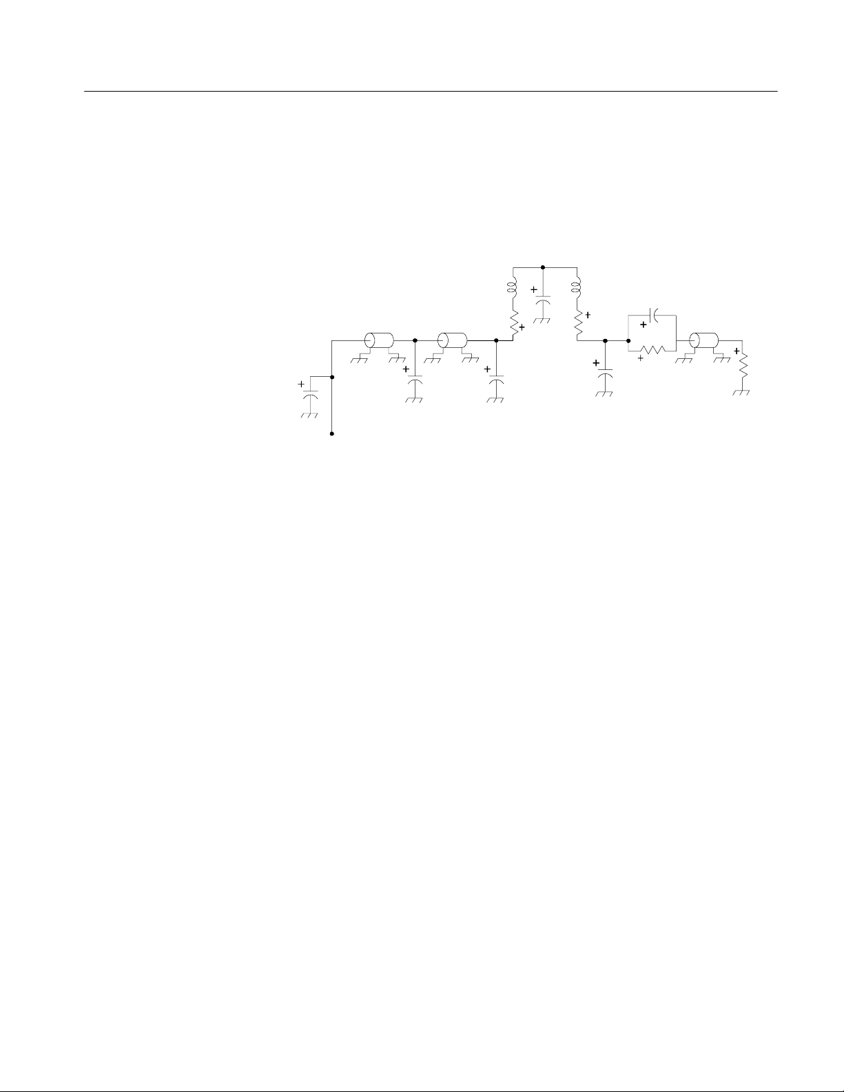
P6419 High-Density Probe Load Model. The following electrical model (see
Figure 18) includes a low-frequency and high-frequency model of the high-density probes.
Low Frequency probe load
0.48 pF
T1 td=17 pS
z0=70 Ω
0.06 pF
T2 td=10 pS
z0=66 Ω
C1
C1
0.22 pF
0.22 pF
High Frequency
probe load
C2
+R1
20k Ω
Ref
Ref - module
GND - TLA520x
2.2 V - TLA7Lx/ Mx/ Nx/ Px/
Qx & TLA6xx
+R1
20k Ω
Ref
Figure 18: High-Density probe load model
Mictor-on-PCB to Compression Adapter Load Model. Refer to Figure 19 for an
electrical model of the Mictor-on-PCB to Compression adapter. The pad cap is
the capacitance of the 0.016 in x 0.032 in pad of the P6419 compression land
footprint. The capacitive load depends upon the distance to the underlying
conductors.
36
td=35 pF
z0=90 Ω
.18 pF .06 pF
.005 Ω
.12 pF
td=17 pF
z0=70 Ω
td=92 pS
z0=57 Ω
.005 Ω
td=10 pF
z0=66 Ω
.22 pF
pad_cap
GND - TLA520x
2.2 V - TLA7Lx/ Mx/ Nx/ Px/
Figure 19: Mictor-on-PCB to Compression adapter load model
P6419 Logic Analyzer Probe Instructions
20K Ω
Ref
Ref - module
Qx & TLA6xx
Page 49
Reference
Compression-on-PCB to P6434 Mictor Adapter Load Model. Refer to Figure 20 for
an electrical model of the Compression-on-PCB to P6434 Mictor adapter. The
pad cap is the capacitance of the 0.016 in x 0.032 in pad of the P6419 compression land footprint. The capacitive load depends upon the distance to the
underlying conductors.
.005 Ω
.12 pF
.7 pF
1.1 pF
1.6 nH
.005 Ω
.23 pF
20K Ω
pad_cap
td=17 pS
z0=70 Ω
1.6 nH
td=35 pS
z0=90 Ω
.18 pF
Figure 20: Compression-on-PCB to P6434 Mictor adapter load model
td = 7 nS
z0 = 75 Ω
75 Ω
P6419 Logic Analyzer Probe Instructions
37
Page 50
Reference
Specifications
Table 9 lists the electrical and mechanical specifications for the P6419 probe.
The electrical specifications apply when the probe is connected between a
compatible logic analyzer and a target system.
Table 9: Electrical and mechanical specifications
Characteristics Description
Number of input channels 17 (16 data channels, 1 clock/qualifier channel)
Threshold accuracy ± 100 mV
Channel-to-channel skew < 100 ps
Input resistance 20 KΩ
Input capacitance 0.7 pF (typical)
Maximum operating signal 8V
Maximum nondestructive i nput
signal to probe
Probe overdrive ± 300 mV or ± 25% of signal swing, whichever is greater.
Minimum sampling period TLA7Lx,Mx,Nx,Px,Qx and
Maximum synchronous clock
rate
Delay from probe tip to module input connector
Probe length 1.9m(75in)
P-P
± 15 V
TLA520x
TLA60x,61x,62x
4ns 2.22 ns
TLA7Lx,Mx,Nx,Px,Qx and
TLA60x,61x,62x
200 MHz 235 MHz
7.33 ns
TLA520x
Table 10 shows the environmental specifications for the P6419 probe. The probe
is designed to meet Tektronix standard 062-2847-00 class 5.
38
P6419 Logic Analyzer Probe Instructions
Page 51
Table 10: Environmental specifications
y
a
Characteristics Description
Temperature
Reference
Maximum operating
Minimum operating + 0 °C(+ 32 °F)
Non-operating −55 °Cto+75 °C(−67 °Fto+167 °F)
Humidity
Operating 5% to 95% relative humidit
Non-operating 5% to 95% relative humidity at up to +30 °C
Altitude
Operating
Non-operating 4.6 km (15,092 ft)
+ 50 °C 〈+122 °F)
tupto+30 °C
5% to 75% relative humidity above +30 °Cupto+50 °C
5% to 75% relative humidity above +30 °Cupto+60 °C
4.6 km (15,092 ft)
P6419 Logic Analyzer Probe Instructions
39
Page 52

Reference
40
P6419 Logic Analyzer Probe Instructions
Page 53

Maintenance
Probe Calibration
Functional Check
The P6419 probe does not require scheduled or periodic maintenance. Use the
procedures listed under Functional Check to check the basic functionality of the
probe.
To confirm that the probes meet or exceed the performance requirements for
published specifications with a compatible TLA7Lx/Mx/Nx/Px/Qx module,
TLA6xx logic analyzer or TLA520x logic analyzer, refer to the Performance
Verification Procedures in the appropriate logic analyzer service manual.
If performing the probe calibration yourself, refer to the appropriate logic
analyzer service manual for the complete calibration procedure. Otherwise,
return the probe to the local Tektronix service center.
NOTE. For the default setup, if you connect probes to any channels other that the
A2 or A3 groups, you must define the groups and channels in the Setup window
before acquiring data on other probe channels.
Connect the logic analyzer probes to a signal source, start an acquisition, and
verify that the acquired data is displayed in either the Listing or Waveform
windows.
If available, use the TLACAL1 fixture to run the performance verification. For
further details, refer to the performance verification procedure in the appropriate
logic analyzer service manual.
Inspection and Cleaning
CAUTION. To prevent damage during the probe connection process, do not touch
the exposed edge of the elastomer.
To maintain a reliable electrical contact, keep the probes free of dirt, dust, and
contaminants. Remove dirt and dust with a soft brush. For more extensive
cleaning, use only a damp cloth. Never use abrasive cleaners or organic solvents.
P6419 Logic Analyzer Probe Instructions
41
Page 54

Maintenance
P6419 Probe Service Procedures
Except for the elastomer holders, the P6419 probe contains no user-replaceable
parts. If probe failures occur, return the entire probe to your Tektronix service
representative for repair.
Repackaging Instructions
If at all possible, use the original packaging to ship or store the probes. If the
original packaging is not available, use a corrugated cardboard shipping carton.
Add cushioning material to prevent the probes from moving around in the
shipping container.
Enclose the following information when shipping the probe to a Tektronix
Service Center:
H The owner’s address
H Name and phone number of a contact person
H Type of probe
H Reason for returning
H A complete description of the service required
Seal the shipping carton. Mark the address of the Tektronix Service Center and
your own return address on the shipping carton in two prominent locations.
42
P6419 Logic Analyzer Probe Instructions
Page 55

Replaceable Parts
This chapter contains a list of the replaceable components for the P6419 probe.
Use this list to identify and order replacement parts.
Parts Ordering Information
Replacement parts are available through your local Tektronix field office or
representative.
Changes to Tektronix products are sometimes made to accommodate improved
components as they come available and to give you the benefit of the latest
improvements. Therefore, when ordering parts, it is important to include the
following information in your order.
H Part number
H Instrument type or model number
H Instrument serial number
H Instrument modification number, if applicable
If you order a part that has been replaced with a different or improved part, your
local Tektronix field office or representative will contact you concerning any
change in part number.
Using the Replaceable Parts List
Replaceable Parts
The P6419 probe contains only the elastomers and nut block as replaceable parts.
If probe failure occurs, return the entire probe to your Tektronix service
representative for repair.
P6419 Logic Analyzer Probe Instructions
43
Page 56
Replaceable Parts
Refer to the following list for replaceable items:
Table 11: Parts list column descriptions
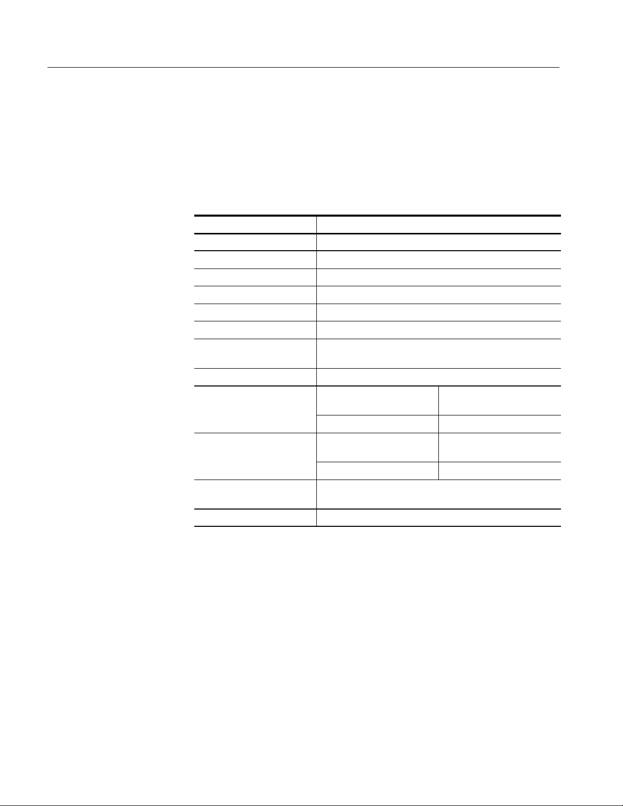
Column Colum n name Description
1 Figure & index number Items in this section reference figure and index numbers to the exploded view illustrations
that follow.
2 Tektronix part number Use this part number when ordering replacement parts from Tektronix.
3 and 4 Serial number Column three indicates the serial number at which the part was first effective. Column four
indicates teh serial number at which the part was discontinued. No entries indicate the part
is good for all serial numbers.
5 Qty This indicates the quantity of parts used.
6 Name & description An item name is separated from the description by a colon (:). Because of space
limitations, an item name may sometimes appear as incomplete. Use the U.S. Federal
Catalog handbook H6-1 for f urt her item name identification.
7 Mfr. code This indicates the code of the actual manufacturer of the part.
8 Mfr. part number This indicates the actual manufacturer’s or vendor’s part number.
Abbreviations
Mfr. Code to Manufacturer
Cross Index
Abbreviations conform to American National Standard ANSI Y1.1--1972.
The table titled Manufacturers Cross Index shows codes, names, and addresses
of manufacturers or vendors of components listed in the parts list.
Table 12: Manufacturers cross index
Mfr
code
80009 TEKTRONIX 14150 SW KARL BRAUN DR
Manufacturer Address City, state, zip code
PO BOX 500
BEAVERTON, OR 97077-0001
44
P6419 Logic Analyzer Probe Instructions
Page 57

Table 13: P6419 replaceable parts list
Figure &
Index
number
21
-1 010-6419-10 1 P6419 PROBE (INCLUDES SHEET OF LABELS AND
Tektronix
part number
020-2451-00 1 P6419 THIN ELASTOMER HOLDER ASSEMBLY,
020-2452-00 1 P6419 THICK ELASTOMER HOLDER ASSEMBLY,
071-1303-XX 1 MANUAL, TECH:INSTRUCTIONS, P6419 80009 071-1303-XX
335-1007-00 1 P6419 PROBE, SHEET OF LABELS 80009 335-1007-00
061-4254-01 1 DATA SHEET; READ THIS FIRST, PRECAUTIONS
220-0255-00 1 NUT BAR ASSEMBLY 80009 220-0255-00
Serial no
effective
Serial no
discont’d
Qty Name & description
PROBE LABELING INSTRUCTIONS)
P6419 STANDARD ACCESSOR IES
(USED WITH NUT BAR), BAG OF 2 (BLACK) (TOTAL
OF 2 ELASTOM ER ASSEMBLIES)
(USED WITH PRESS-IN NUT), BAG OF 2 (GRAY)
(TOTAL OF 2 ELASTOMER ASSEMBLIES)
FOR HANDLING ELASTOMER BASED COMPRESSION PROBES, GOLDEN ROD;DP
Replaceable Parts
Mfr.
code
80009 010-6419-10
80009 020-2451-00
80009 020-2452-00
80009 061-4252-01
Mfr. part
number
1
Figure 21: P6419 logic analyzer probe
P6419 Logic Analyzer Probe Instructions
45
Page 58
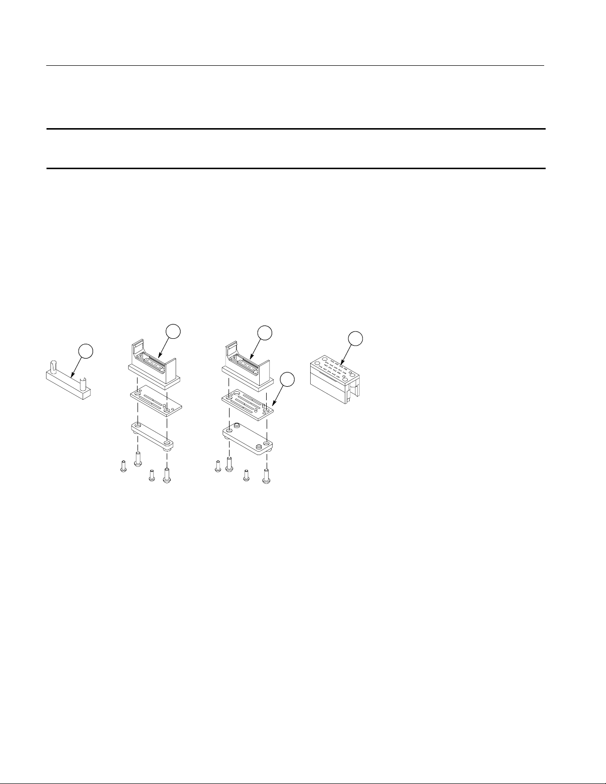
Replaceable Parts
Table 14: Adapter replaceable parts list
Figure &
Index
number
22 P6419 OPTI ONAL ACCESSORI ES
-1 020-2453-00 1 NUT BAR ASSEMBLY, BAG OF 2 80009 020-2453-00
-2 020-2455-00 1 17 CH COMPRESSION-ON-PCB TO P6434 MICTOR
-3 020-2456-00 1 34 CH COMPRESSION-ON-PCB TO P6434 MICTOR
-4 020-2457-00 1 34 CH MICTOR-ON-PCB TO COMPRESSION
-5 352-1095-00 1 ELASTOMER ASSEMBLY 80009 352-1095-00
Tektronix
part number
Serial no
effective
Serial no
discont’d
Qty Name & description
ADAPTER
ADAPTER
ADAPTER
Mfr.
code
80009 020-2455-00
80009 020-2456-00
80009 020-2457-00
Mfr. part
number
2
1
3
5
4
Figure 22: Compression-on-PCB to P6434 Mictor adapter
46
P6419 Logic Analyzer Probe Instructions
Page 59

Index
Page 60

Page 61

Index
A
Adapters
Compression on PCB to Mictor, 3
Mictor on PCB to Compression, 2
Address, Tektronix, viii
C
Cleaning
compression footprints, 8
probe heads, 8
Compression on PCB to Mictor adapter, 3
Connecting
probes to logic analyzer, 7
probes to target system, 10
Contacting Tektronix, viii
D
Designing an interface
electrical considerations, 35
land footprints, 27
mechanical considerations, 30
signal names, 19
L
Labels, attaching to the probe, 5
Land footprints, 27
P6419 High Density Probe, 28
Load model
Compression--on--PCB to P6434 Mictor adapter, 37
Mictor--on-- PCB to Compression adapter, 36
P6419 High Density Probe , 36
Logic analyzer, connecting probes, 7
M
Mechanical considerations
land footprint requirements for P6419 probe, 30
land footprint requirements for the Compression on
PCB to Mictor adapter, 32
physical attachment requirements for P6419 probe,
33
physical attachment requirements for the Compres-
sion on PCB to Mictor and Mictor on PCB to
Compression adapters, 35
Mictor on PCB to Compression adapter, 2
N
E
Elastomer holder, installing Press--in nuts, 11
Electrical considerations
Mictor--on-- PCB to Compression adapter, 36
P6419 High Density Probe load model, 36
Compression--on--PCB to P6434 Mictor adapter, 37
Transmission lines, 35
F
Footprints, land, 27
P6419 High Density Probe, 28
H
High resolution timing modes, 18
K
Keepout area, 31, 33
Nut bar, 10
P
Phone number, Tektronix, viii
Press--in nuts, 11
Probes
cleaning the P6419 Compression footprints, 8
cleaning the P6419 probe head, 8
connecting probes to the logic analyzer, 7
connecting probes to the target system, 10
Product description
Compression on PCB to Mictor adapter, 3
Mictor on PCB to Compression adapter, 2
Product support, contact information, viii
R
Range recognition, 19
Requirements
P6419 Logic Analyzer Probe Instructions
Index- 1
Page 62

Index
land footprint for the Compression on PCB to Mictor
adapter, 32
land footprints for P6419 Probe, 30
physical attachment for the Compression on PCB to
Mictor and Mictor on PCB to Compression
adapters, 35
physical attachment for the P6419 probe, 33
S
Service support, contact information, viii
Signal names, 19
T
Target system, connecting probes, 10
S
Service support, contact information, viii
Signal names, 19
T
Target system, connecting probes, 10
Technical support, contact information, viii
Tektronix, contacting, viii
Timing modes, High resolution, 18
Transmission Lines, 35
U
URL, Tektronix, viii
W
Web site address, Tektronix, viii
Index- 2
P6419 Logic Analyzer Probe Instructions
 Loading...