

Page 1

Instruction Manual
P6339A
500 MHz Buffered Passive Probe
071-0178-01
Warning
The servicing instructions are for use by qualified
personnel only. To avoid personal injury, do not
perform any servicing unless you are qualified to
do so. Refer to all safety summaries prior to
performing service.
www.tektronix.com
Page 2

Copyright © Tektronix, Inc. All rights reserved.
Tektronix products are covered by U.S. and foreign patents, issued and
pending. Information in this publication supercedes that in all previously
published material. Specifications and price change privileges reserved.
Tektronix, Inc., P.O. Box 500, Beaverton, OR 97077
TEKTRONIX, TEK, TEKPROBE, and SureFoot are registered trademarks of
Tektronix, Inc. KlipChip is a trademark of Tektronix, Inc.
Copyright © Tektronix, Inc. All rights reserved.
Page 3

WARRANTY
T ektronix warrants that the products that it manufactures and sells will be free from defects
in materials and workmanship for a period of one (1) year from the date of shipment. If a
product proves defective during this warranty period, Tektronix, at its option, either will
repair the defective product without charge for parts and labor, or will provide a
replacement in exchange for the defective product.
In order to obtain service under this warranty, Customer must notify Tektronix of the
defect before the expiration of the warranty period and make suitable arrangements for the
performance of service. Customer shall be responsible for packaging and shipping the
defective product to the service center designated by Tektronix, with shipping charges
prepaid. T ektronix shall pay for the return of the product to Customer if the shipment is to
a location within the country in which the Tektronix service center is located. Customer
shall be responsible for paying all shipping charges, duties, taxes, and any other charges for
products returned to any other locations.
This warranty shall not apply to any defect, failure or damage caused by improper use or
improper or inadequate maintenance and care. Tektronix shall not be obligated to furnish
service under this warranty a) to repair damage resulting from attempts by personnel other
than Tektronix representatives to install, repair or service the product; b) to repair damage
resulting from improper use or connection to incompatible equipment; c) to repair any
damage or malfunction caused by the use of non-Tektronix supplies; or d) to service a
product that has been modified or integrated with other products when the effect of such
modification or integration increases the time or difficulty of servicing the product.
THIS WARRANTY IS GIVEN BY TEKTRONIX IN LIEU OF ANY OTHER
WARRANTIES, EXPRESS OR IMPLIED. TEKTRONIX AND ITS VENDORS
DISCLAIM ANY IMPLIED WARRANTIES OF MERCHANTABILITY OR
FITNESS FOR A PARTICULAR PURPOSE. TEKTRONIX’ RESPONSIBILITY
TO REPAIR OR REPLACE DEFECTIVE PRODUCTS IS THE SOLE AND
EXCLUSIVE REMEDY PROVIDED TO THE CUSTOMER FOR BREACH OF
THIS WARRANTY. TEKTRONIX AND ITS VENDORS WILL NOT BE LIABLE
FOR ANY INDIRECT, SPECIAL, INCIDENTAL, OR CONSEQUENTIAL
DAMAGES IRRESPECTIVE OF WHETHER TEKTRONIX OR THE VENDOR
HAS ADVANCE NOTICE OF THE POSSIBILITY OF SUCH DAMAGES.
Page 4

Page 5

Table of Contents
General Safety Summary v. . . . . . . . . . . . . . . . . . . . . . . . . . . .
Service Safety Summary vii. . . . . . . . . . . . . . . . . . . . . . . . . . . . .
Contacting Tektronix ix. . . . . . . . . . . . . . . . . . . . . . . . . . . . . . . .
Getting Started 1. . . . . . . . . . . . . . . . . . . . . . . . . . . . . . . . . . . . .
Features and Accessories 1. . . . . . . . . . . . . . . . . . . . . . . . . . . . . .
Optional Accessories 4. . . . . . . . . . . . . . . . . . . . . . . . . . . . . . . . .
Functional Check 4. . . . . . . . . . . . . . . . . . . . . . . . . . . . . . . . . . . .
T ekProbe Communication 5. . . . . . . . . . . . . . . . . . . . . . . . . .
DC Offset 5. . . . . . . . . . . . . . . . . . . . . . . . . . . . . . . . . . . . . . .
DC Gain and Attenuation 6. . . . . . . . . . . . . . . . . . . . . . . . . . .
Operating Basics 7. . . . . . . . . . . . . . . . . . . . . . . . . . . . . . . . . . .
Probe Compensation 7. . . . . . . . . . . . . . . . . . . . . . . . . . . . . . . . .
Maximum Input Voltage 8. . . . . . . . . . . . . . . . . . . . . . . . . . . . . .
High-Frequency Probe Connections 8. . . . . . . . . . . . . . . . . . . . .
Specifications 9. . . . . . . . . . . . . . . . . . . . . . . . . . . . . . . . . . . . . .
Adjustment and Verification Procedures 15. . . . . . . . . . . . . . .
Equipment Required 16. . . . . . . . . . . . . . . . . . . . . . . . . . . . . . . . .
Preparation 17. . . . . . . . . . . . . . . . . . . . . . . . . . . . . . . . . . . . . . . . .
Remove the Top Cover 17. . . . . . . . . . . . . . . . . . . . . . . . . . . .
Prepare the Equipment 17. . . . . . . . . . . . . . . . . . . . . . . . . . . . .
Adjustment Locations 18. . . . . . . . . . . . . . . . . . . . . . . . . . . . .
Procedures 19. . . . . . . . . . . . . . . . . . . . . . . . . . . . . . . . . . . . . . . . .
HF Adjust 19. . . . . . . . . . . . . . . . . . . . . . . . . . . . . . . . . . . . . . .
Compensate the Probe 20. . . . . . . . . . . . . . . . . . . . . . . . . . . . .
Rise Time and Aberrations 21. . . . . . . . . . . . . . . . . . . . . . . . .
Output Zero Adjust 22. . . . . . . . . . . . . . . . . . . . . . . . . . . . . . .
DC Attenuation Accuracy 22. . . . . . . . . . . . . . . . . . . . . . . . . .
Rise Time Check 25. . . . . . . . . . . . . . . . . . . . . . . . . . . . . . . . .
Reset DIP Switches and Install Cover 26. . . . . . . . . . . . . . . . .
Test Record 27. . . . . . . . . . . . . . . . . . . . . . . . . . . . . . . . . . . . . . . .
P6339A Instruction Manual
i
Page 6

Table of Contents
Maintenance 31. . . . . . . . . . . . . . . . . . . . . . . . . . . . . . . . . . . . . . .
Cleaning 31. . . . . . . . . . . . . . . . . . . . . . . . . . . . . . . . . . . . . . . . . . .
Replacing TekProbe Interface Pins 32. . . . . . . . . . . . . . . . . . . . . .
Removing and Replacing the TekProbe Interface Collar 33. . . . .
Removing and Replacing the Cable Assembly 34. . . . . . . . . . . . .
Replaceable Parts 35. . . . . . . . . . . . . . . . . . . . . . . . . . . . . . . . . . .
ii
P6339A Instruction Manual
Page 7

List of Figures
Figure 1: SMK4 Micro KlipChip adapter 4. . . . . . . . . . . . . . .
Figure 2: Probe compensation waveforms 7. . . . . . . . . . . . . .
Figure 3: Ground lead effects 8. . . . . . . . . . . . . . . . . . . . . . . . .
Figure 4: Voltage derating, typical 1 1. . . . . . . . . . . . . . . . . . . . .
Figure 5: Input impedance, typical 12. . . . . . . . . . . . . . . . . . . .
Figure 6: Input phase, typical 12. . . . . . . . . . . . . . . . . . . . . . . . .
Figure 7: Location adjustments and DIP switches 18. . . . . . . .
Figure 8: Setup for probe compensation and high fr equency
adjustment 20. . . . . . . . . . . . . . . . . . . . . . . . . . . . . . . . . . . . .
Table of Contents
Figure 9: Probe compensation waveforms 20. . . . . . . . . . . . . .
Figure 10: Setup for rise time and aberrations 21. . . . . . . . . . .
Figure 11: Setup for the output offset adjustment 22. . . . . . . .
Figure 12: Setup for DC attenuation accuracy 23. . . . . . . . . . .
Figure 13: Setup for rise time check 25. . . . . . . . . . . . . . . . . . .
Figure 14: Replacing TekProbe interface pins 32. . . . . . . . . . .
Figure 15: Replacing the TekProbe collar 33. . . . . . . . . . . . . . .
Figure 16: Replacing the cable assembly 34. . . . . . . . . . . . . . . .
Figure 17: P6339A replaceable parts and standard
accessories 35. . . . . . . . . . . . . . . . . . . . . . . . . . . . . . . . . . . . . .
P6339A Instruction Manual
iii
Page 8

Table of Contents
List of Tables
Table 1: Features and accessories 2. . . . . . . . . . . . . . . . . . . . .
Table 2: Electrical specifications 9. . . . . . . . . . . . . . . . . . . . . .
Table 3: Environmental characteristics 11. . . . . . . . . . . . . . . .
Table 4: Physical characteristics 13. . . . . . . . . . . . . . . . . . . . . .
Table 5: Certifications and compliances 13. . . . . . . . . . . . . . . .
Table 6: Test equipment 16. . . . . . . . . . . . . . . . . . . . . . . . . . . . .
Table 7: DIP switch/attenuation settings 19. . . . . . . . . . . . . . .
Table 8: Input voltages for DC attenuation accuracy
adjustment 24. . . . . . . . . . . . . . . . . . . . . . . . . . . . . . . . . . . . .
Table 9: Settings for rise time check 26. . . . . . . . . . . . . . . . . . .
iv
P6339A Instruction Manual
Page 9

General Safety Summary
Review the following safety precautions to avoid injury and prevent
damage to this product or any products connected to it. To avoid
potential hazards, use this product only as specified.
Only qualified personnel should perform service procedures.
To Avoid Fire or Personal Injury
Connect and Disconnect Properly. Connect the probe output to the
measurement instrument before connecting the probe to the circuit
under test. Disconnect the probe input and the probe ground from the
circuit under test before disconnecting the probe from the measurement instrument.
Observe All Terminal Ratings. To avoid fire or shock hazard, observe all
ratings and markings on the product. Consult the product manual for
further ratings information before making connections to the product.
The common terminal is at ground potential. Do not connect the
common terminal to elevated voltages.
Do Not Operate Without Covers. Do not operate this product with
covers or panels removed.
Do Not Operate With Suspected Failures. If you suspect there is damage
to this product, have it inspected by qualified service personnel.
Do Not Operate in Wet/Damp Conditions.
Do Not Operate in an Explosive Atmosphere.
Keep Product Surfaces Clean and Dry.
P6339A Instruction Manual
v
Page 10

General Safety Summary
Safety Terms and Symbols
Terms in This Manual. These terms may appear in this manual:
WARNING. Warning statements identify conditions or practices that
could result in injury or loss of life.
CAUTION. Caution statements identify conditions or practices that
could result in damage to this product or other property.
Terms on the Product. These terms may appear on the product:
DANGER indicates an injury hazard immediately accessible as you
read the marking.
WARNING indicates an injury hazard not immediately accessible as
you read the marking.
CAUTION indicates a hazard to property including the product.
Symbols on the Product. These symbols may appear on the product:
CAUTION
Refer to Manual
WARNING
High Voltage
Double
Insulated
Protective Ground
(Earth) Terminal
vi
P6339A Instruction Manual
Page 11

Service Safety Summary
Only qualified personnel should perform service procedures. Read
this Service Safety Summary and the General Safety Summary before
performing any service procedures.
Do Not Service Alone. Do not perform internal service or adjustments
of this product unless another person capable of rendering first aid
and resuscitation is present.
Use Care When Servicing with Power On. Dangerous voltages or currents
may exist in this product. Disconnect power, remove battery (if
applicable), and disconnect test leads before removing protective
panels, soldering, or replacing components.
To avoid electric shock, do not touch exposed connections.
P6339A Instruction Manual
vii
Page 12

Service Safety Summary
viii
P6339A Instruction Manual
Page 13

Contacting Tektronix
Phone 1-800-833-9200*
Address Tektronix, Inc.
Department or name (if known)
14200 SW Karl Braun Drive
P.O. Box 500
Beaverton, OR 97077
USA
Web site www.tektronix.com
Sales
support
Service
support
Technical
support
* This phone number is toll free in North America. After office
hours, please leave a voice mail message.
Outside North America, contact a T ektronix sales office or
distributor; see the Tektronix web site for a list of offices.
1-800-833-9200, select option 1*
1-800-833-9200, select option 2*
Email: techsupport@tektronix.com
1-800-833-9200, select option 3*
1-503-627-2400
6:00 a.m. – 5:00 p.m. Pacific time
P6339A Instruction Manual
ix
Page 14

Contacting Tektronix
x
P6339A Instruction Manual
Page 15

Getting Started
The P6339A Buffered Passive Probe is specifically designed for
Tektronix oscilloscopes such as the TDS 794D. Each high-bandwidth
input of these oscilloscopes has a fixed 50 W impedance and a
TekProbe III interface. To allow a broader range of measurement
applications, the P6339A probe passively attenuates and then
actively buffers the signal to match the 50 W input impedance.
Key probe specifications include the following:
H 500 MHz bandwidth
H 8 pF input capacitance
H 10 MW passive input (10X)
The oscilloscope settings control the following parameters of the
buffered probe output:
H Attenuation and gain
H AC/DC coupling
H Bandwidth limit
H DC offset
For a complete list of specifications, refer to page 9.
Features and Accessories
Table 1 illustrates the user features of the P6339A Buffered Passive
Probe and standard accessories. In addition to those items shown, the
standard accessories also include the following:
H Adjustment tool for probe compensation
H Accessory pouch
H Instructions (this manual)
P6339A Instruction Manual
1
Page 16

Getting Started
Table 1: Features and accessories
Feature/Accessory Description Applications/Notes
Marker bands Color codes the probe to the
oscilloscope input when more
than one probe is in use. Clip
one band around the strain relief
of the probe head and the
matching band on the strain
relief of the probe compensation
box.
Ground collar
Ground lead
Ridged probe cover
Short ground
lead
Retractable
hook tip
SMT KlipChip
and ground
lead
Connects the probe ground to a
ground reference close to the
signal source.
To install, slip the ground collar
onto the probe head then screw
the ridged probe cover down
over the probe tip. Insert the
socket end of the ground lead
into the hole of the ground
collar.
Connects the probe tip to wires
and component leads for handsfree measurement.
NOTE. For a solid connection,
firmly push and twist the hook
tip onto the probe tip before
using.
Connects the probe ground to
small or hard to reach ground
reference points. The ground
lead also connects to a variety
of optional accessories.
2
P6339A Instruction Manual
Page 17

T able 1: Features and accessories (cont.)
Feature/Accessory Applications/NotesDescription
Getting Started
Ground lead
with insulated
alligator clip
SureFoot
probe tip set
Guard Keeps fingers away from the
Guard
Connects the probe ground to
ground reference.
Provides fault-free probing of
SMD packages that have lead
spacings of 0.50 mm/20 mil
(red), 0.65 mm/25 mil (blue), or
50 mil (orange).
probe tip for protection against
electric shock.
WARNING. To avoid electric shock when using the probe, keep fingers
behind the guard on the probe body.
Ordering information for replaceable parts and standard accessories
begins on page 35.
P6339A Instruction Manual
3
Page 18

Getting Started
Optional Accessories
Recommended optional accessories include the SMK4 shown in
Figure 1. This adapter enables connections to very small leads.
Figure 1: SMK4 Micro KlipChip adapter
The P6339A probe is fully compatible with the entire line of 3.5 mm
(compact) accessories.
Ordering information for optional accessories begins on page 35.
Functional Check
Use the functional check procedures in this section to verify basic
probe operation with Tektronix oscilloscopes such as the TDS 794D.
Because this is a functional check, no tolerances are given for the
measured values.
NOTE. To verify warranted specifications and to adjust the probe,
qualified service personnel may use the adjustment and verification
procedures that begin on page 15.
4
P6339A Instruction Manual
Page 19

Getting Started
T ekProbe Communication
This procedure verifies the operation of the TekProbe III interface.
1. Turn on the oscilloscope. Wait for the power up self test to
complete.
2. Disconnect all cables or probes from the inputs.
3. Press the Autoset button.
4. Press the CH 1 button.
5. Use the Vertical Scale knob to set the vertical scale factor to
100 mV/div.
6. Press the Vertical Menu button.
7. Attach the probe to the CH 1 input.
8. Select the Coupling menu.
9. Verify that AC and DC coupling and GND are selectable by
switching between them.
10.Verify that the channel 1 scale factor is selectable from 10mV/div
to 100V/div.
11. Verify that the Bandwidth is selectable between Full, 20MHz and
150MHz (2nd button along lower bezel).
DC Offset
This procedure verifies that the oscilloscope can compensate for the
DC offset of each volts/division range of the the P6339A probe.
1. With the probe attached to channel 1, set the oscilloscope to the
lowest volts/division setting (10 mV/div).
2. Set the input coupling to GND and set the ground reference to
center screen.
3. Install a retractable hook tip and ground lead on the probe head.
4. Short the input of the probe to probe ground by connecting a
short jumper from the hook tip to the ground lead.
5. Set the coupling to DC.
P6339A Instruction Manual
5
Page 20

Getting Started
6. Check that the ground reference for each volts per division range
DC Gain and Attenuation
This procedure verifies the correct gain and attenuation of each
volts/division range of the probe.
1. With the probe attached to channel 1, set the oscilloscope to the
2. Connect the output of a standard amplitude calibration generator
3. Set the oscilloscope to DC coupling.
4. For each volts per division range from 10mV/div to 100V/div,
from 10mV/div to 100V/div stays near center screen.
lowest volts/division setting (10 mV/div).
or calibrated DC source to the input of the probe.
adjust the generator or DC source to display four or five divisions
of vertical deflection and check that the measured value of the
input agrees with the output of the generator or DC source.
This completes the functional check procedure.
6
P6339A Instruction Manual
Page 21

Operating Basics
To obtain the best performance from the P6339A probe, compensate
the probe as needed, observe the maximum input voltage and make
appropriate probe connections.
Probe Compensation
Due to variations in oscilloscope input characteristics, probe
low-frequency compensation may need adjustment after moving the
probe from one oscilloscope to another . If a 1 kHz calibrated square
wave displayed at 1 ms/division shows significant differences
between the leading and trailing edges, perform the following steps
to optimize low-frequency compensation.
1. Connect the probe to the calibration signal on the oscilloscope
front panel.
2. Press AUTOSET or otherwise adjust your digitizing oscilloscope
to display a meaningful waveform.
3. Adjust the trimmer in the probe (accessible through the
compensation box) until you see a perfectly flat-top square wave
on the display. See Figure 2.
Undercompensated Overcompensated Properly compensated
Figure 2: Probe compensation waveforms
P6339A Instruction Manual
7
Page 22

Operating Basics
Maximum Input Voltage
Estimate the RMS voltage of a pulse signal before measurement. The
combination of pulse width, duty factor, and DC level determine the
RMS signal voltage. Depending on the application or “installation
category,” this voltage must not exceed the ratings listed in the
Specifications section on page 10.
WARNING. To avoid electric shock when using the probe, do not
touch the metallic portions of the probe head while connected to a
voltage source.
High-Frequency Probe Connections
To minimize inductive effects that cause ringing at high frequencies,
keep all signal and ground leads as short as possible (see Figure 3).
Accessories are included with the probe that provide convenient
means to make short connections (see page 2).
100
90
10
0%
Short ground lead
3“ Ground lead
Figure 3: Ground lead effects
8
P6339A Instruction Manual
Page 23

Specifications
All specifications in Table 2 apply to the probe only unless marked
as system. The system specifications apply when the P6339A probe
is operated with a TDS 794D in an environment that does not exceed
the limits described in Table 3 on page 11.
All specifications are warranted unless marked as typical. The
n symbol indicates warranted specifications that have checks in the
Adjustment Procedures section.
T able 2: Electrical specifications
System input resistance, typical
System input capacitance, typical 8.0 pF at 1 kHz (DC coupled), see Figure 5
System bandwidth, calculated DC to 500 MHz at 50 mV/div
System dynamic range, typical ± 10 divisions at each V/div setting except
System offset range, typical ± 10 divisions
System output zero, typical ± 0.6 division or less displayed on screen
Aberrations, typical (probe only) +8%, –6% at 10 mV/div
10 MW at DC (DC coupled), see Figure 5
50 V and 100 V/div
after probe cal
+16%, –6% at 20 mV, 50 mV, 0.1 V, and
0.2 V/div
+18%, –6% at 0.5 V/div
+21%, –6% at 1 V/div
+22%, –6% at 2 V/div
+24%, –6% at 5 V/div
1
+35%, –17% at 10 V/div
AC coupling, typical lower bandwidth < 10 Hz
P6339A Instruction Manual
9
Page 24

Specifications
T able 2: Electrical specifications (cont.)
n
Output zero (probe only)
± 20 mV at 10 mV/div,
± 10 mV at 20 mV/div,
± 5 mV at all other V/div settings
n DC attenuation accuracy (probe only)
± 2.0 % at 10 mV, 20 mV, 50 mV, 0.1 V,
0.2 V, 0.5 V, 1 V, 2 V, 5 V, 10 V, 20 V, and
50 V/div
± 4.0 % at 100 V/div
n Rise time (probe only)
1.4 ns at 10 mV/div
875 ps at 20 mV/div
700 ps at 50 mV, 0.1 V, 0.2 V, 0.5 V, 1 V,
2 V, and 5 V/div
870 ps at 10 V/div
Required output termination
50 W
Bandwidth limit frequencies (–3 dB), typical 20 MHz and 150 MHz
Time delay, typical 7.8 ns ± 1 ns
Maximum rated input voltage, probe tip to
earth ground
Overvoltage category I:
600 V
(DC + peak AC)
PK
Overvoltage category II:
300 V
RMS
Category III:
150 V
RMS
Voltage derating, typical See Figure 4
Input impedance, typical See Figure 5
Input phase, typical See Figure 6
1
Full dynamic range at 50 V and 100 V/div would exceed the safety rating of
the probe.
10
P6339A Instruction Manual
Page 25
Specifications
T able 3: Environmental characteristics
Temperature Operating:
+10_ C to + 50_ C (+50_ F to +122_ F)
Nonoperating
–22_ C to +60_ C (–7.6_ F to +140_ F)
Humidity Operating and Nonoperating:
Five cycles (120 hr total) at 80% to 85%
relative humidity
Altitude, operating < 2000 m (< 6,562 ft), rated ranges
2000 to 5000 m (6,562 to 16,404 ft) voltage
ratings reduced to 300 V CAT I and 150 V
CAT II
Altitude, non-operating < 15,240 meters (50,000 ft)
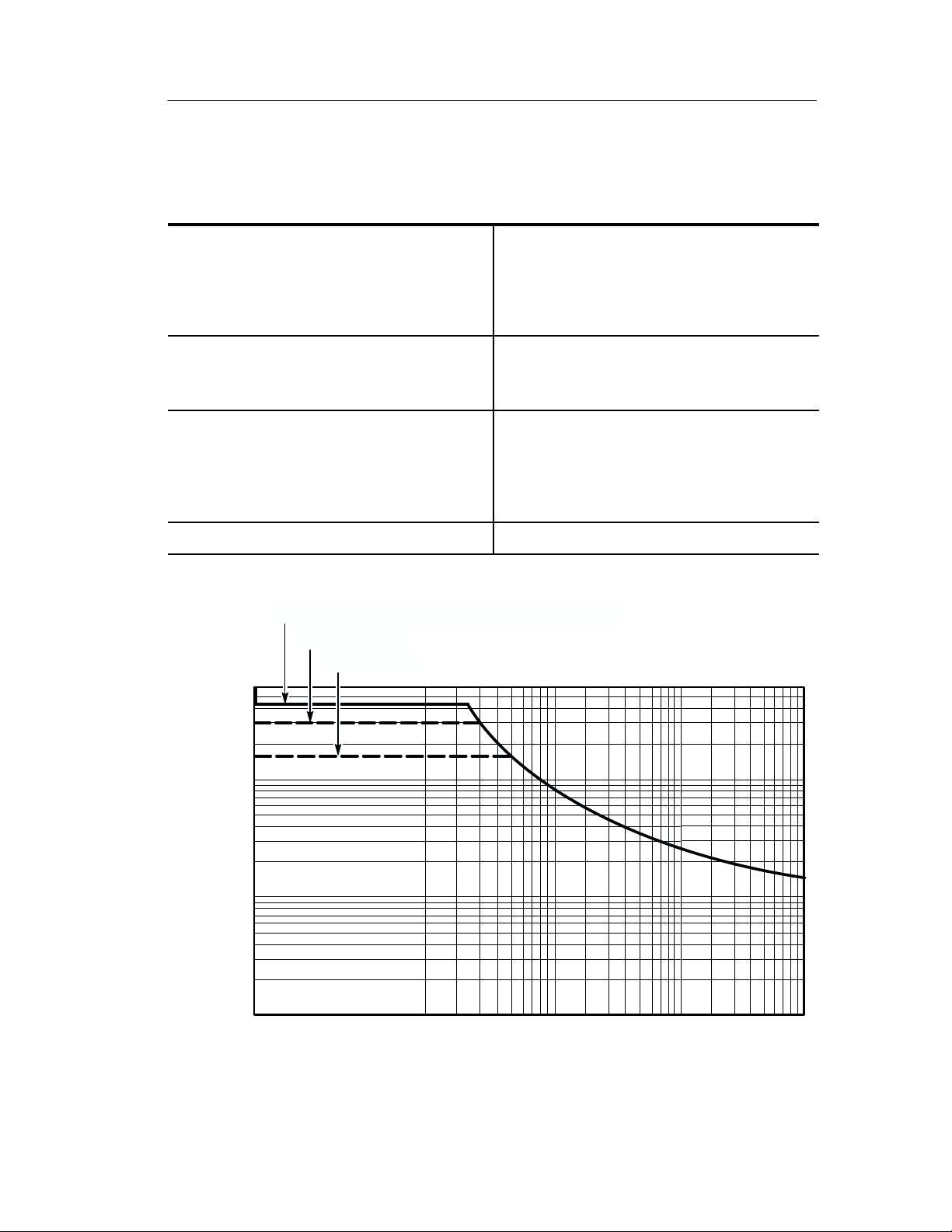
Category I, 420 V
and 600 V
RMS
(DC + peak AC
)
Category II
Category III
600V
400V
300V
200V
100V
AC
RMS
Voltage
10V
0
Figure 4: Voltage derating, typical
P6339A Instruction Manual
5M 50M
10M 100M1M
Frequency (Hz)
1G
11
Page 26

Specifications
10 MW
1MW
100 kW
10 kW
1 kW
100 W
1 k100
10 k 100 k 1 M 10 M 100 M
Figure 5: Input impedance, typical
0_
-10_
-20_
-30_
-40_
-50_
-60_
-70_
-80_
1 G
Frequency (Hz)
-90_
100
Figure 6: Input phase, typical
12
10 k 100 k 1 M 10 M 100 M1 k10
Frequency (Hz)
1 G
P6339A Instruction Manual
Page 27

Specifications
Table 4 lists the physical characteristics of the P6339A probe.
T able 4: Physical characteristics
Weight, typical Shipping weight: 515 g (1.2 lbs) including
shipping materials
Net weight: 185 g (0.41 lbs), probe only
Cable length, typical 1.3 m (51.18 in)
Table 5 lists the certifications and compliances.
T able 5: Certifications and compliances
EC Declaration of
Conformity – Low
Voltage
U.S. Nationally
Recognized Testing
Laboratory Listing
Canadian
Certification
Compliance was demonstrated to the following specification as
listed in the Official Journal of the European Union:
Low Voltage Directive 73/23/EEC, amended by 93/69/EEC
EN 61010-2-031:1994
Particular requirements for hand-held probe assemblies
for electrical measurement and test equipment.
UL3111-1
Standard for electrical measuring and test equipment.
IEC61010-2-031:1994
Particular requirements for hand-held probe assemblies
for electrical measurement and test equipment.
CAN/CSA C22.2 No. 1010.1
Safety requirements for electrical equipment for
measurement, control, and laboratory use.
CAN/CSA C22.2 No. 1010.2.031:1994
Particular requirements for hand-held probe assemblies
for electrical measurement and test equipment.
Additional
Compliance
IEC61010-1/A2
P6339A Instruction Manual
Safety requirements for electrical equipment for
measurement, control, and laboratory use.
13
Page 28

Specifications
T able 5: Certifications and compliances (cont.)
Installation
(Overvoltage)
Category
Pollution Degree A measure of the contaminates that could occur in the environment
Terminals on this product may have different installation
(overvoltage) category designations. The installation categories are:
CAT III Distribution-level mains (usually permanently connected).
Equipment at this level is typically in a fixed industrial
location.
CAT II Local-level mains (wall sockets). Equipment at this level
includes appliances, portable tools, and similar products.
Equipment is usually cord-connected.
CAT I Secondary (signal level) or battery operated circuits of
electronic equipment.
around and within a product. Typically the internal environment
inside a product is considered to be the same as the external.
Products should be used only in the environment for which they are
rated.
Pollution Degree 2
Normally only dry, nonconductive pollution occurs.
Occasionally a temporary conductivity that is caused by
condensation must be expected. This location is a
typical office/home environment. Temporary
condensation occurs only when the product is out of
service.
14
P6339A Instruction Manual
Page 29

WARNING
The following servicing instructions are for use only by
qualified personnel. To avoid injury, do not perform any
servicing other than that stated in the operating instructions
unless you are qualified to do so. Refer to all safety
summaries before performing any service.
Page 30

Page 31

Adjustment and Verification Procedures
Use the following procedures to adjust and verify the P6339A
Buffered Passive Probe to warranted specifications. Before beginning
these procedures, photocopy the test record on pages 27 through 29
and use it to record test results. The recommended adjustment and
verification interval is one year .
These procedures adjust and/or verify the following:
H High frequency (adjust)
H Probe compensation (adjust)
H Rise time and aberrations (adjust)
H Output zero (adjust and/or verify)
H DC attenuation accuracy (adjust and verify)
H Rise time (verify)
WARNING. These procedures are for use by qualified service
personnel only .
P6339A Instruction Manual
15
Page 32

Adjustment and Verification Procedures
Equipment Required
Table 6 lists the equipment required to perform these procedures.
The types and quantities of connectors may vary depending on the
specific equipment you use.
Table 6: Test equipment
Description Minimum requirements Example product
Oscilloscope TekProbe interface,
≤ 267 ps risetime
Probe power supply Compatible with the Tek-
Probe interface
Calibrated DC voltage
source
Digital multimeter DC Accuracy ≤ 0.1%,
High amplitude pulse
generator
Male BNC to probe tip
adapter
Male BNC to 50 W
probe tip adapter
BNC cable
Dual-male-banana-to-
female BNC adapter
Adjustable from 0 V to
400 V with accuracy
≤ 0.05%.
≤ 400 mV range
0 to 50 V pulse, ≤ 250 ps
rise time
Straight-thru 013-0226-00
50 W nominal
50 W, 1%, precision
As per description 103-0090-00
Tektronix TDS694C
Tektronix Type 1103
Wavetek 9100
Fluke 87 or equivalent
Picosecond Pulse Labs
2700C or 2700B
013-0227-00
012-0482-00
16
Precision inline BNC
terminator
Probe tip shorting
connector
In-line attenuator
50 W ± 0.1%
As per description
50 W, 10X
011-0129-00
011-0059-02
P6339A Instruction Manual
Page 33

Preparation
Prepare the probe for adjustment as follows:
Remove the Top Cover
1. Remove the four screws that attach the top cover to the
compensation box.
2. Remove the top cover .
Prepare the Equipment
1. Connect the male BNC to probe tip adapter (013-0226-00) to the
input of the probe.
2. Attach the probe to the 1103 TekProbe Power Supply.
Adjustment and Verification Procedures
3. If necessary, set the line selector to the correct voltage.
4. Turn on the 1103 power supply.
5. Set the offset button to the off position (button not illuminated).
6. Allow at least 20 minutes for the equipment to warm up.
NOTE. Ambient temperature must be within 20_ C to 30_ C when you
adjust the probe.
P6339A Instruction Manual
17
Page 34

Adjustment and Verification Procedures
Adjustment Locations
Figure 7 shows the locations of the adjustments and the DIP switches
(S1) that manually set the probe attenuation (gain) range.
R1 C4
C7
R3
S1
X1
X10
A1
A0
S1
G3
G2
G1
G0
HF
1
0
HF AdjustLF COMP
10m 20m 50m .2 .5 100
10m 20m 50m .2 .5 100
1251020
TP2
50
GAIN
Offset,
X1
DIP switches shown in
“1” position
Offset, X10
Figure 7: Location adjustments and DIP switches
18
Offset, X100
P6339A Instruction Manual
Page 35

Because some of these procedures use the TekProbe 1103 Power
Supply, there is no automatic control of the probe attenuation. You
must manually set the required attenuation for these procedures
according to Table 7.
Table 7: DIP switch/attenuation settings
Adjustment and Verification Procedures
Atten.
setting
10 mV 0 1 0 1 0 0 0 1 1 1.0000
20 mV 0 0 1 0 2 0.5000
50 mV
0.2 V 0 1 0 0 10 0.1000
0.5 V 0 1 0 1 25 0.04000
1 V 1 0 0 0 0 0 1 1 50 0.02000
2 V 0 1 0 0 100 0.01000
5 V 0 1 0 1 250 0.00400
10 V 1 0 1 0 0 0 1 1 500 0.00200
20 V 0 1 0 0 1000 0.00100
50 V 0 1 0 1 2500 0.000400
100 V 1 1 0 1 5000 0.000200
1
X10 X1 A1 A0
1
G3 G2 G1 G0
0 0 1 1 5 0.2000
During normal operation, the probe attenuation for 50 mV/div is the same
System
atten.
System
gain
as 0.1 V/div and the oscilloscope automatically displays the correct
waveform. With the 1103, there are no adjustments for 0.1 V/div.
Procedures
Perform the adjustment and verification procedures in order .
HF Adjust
1. Setup the equipment as shown in Figure 8 on page 20. (For this
procedure, the probe tip does not have to be connected to the
probe compensation signal.)
P6339A Instruction Manual
19
Page 36

Adjustment and Verification Procedures
2. Measure the voltage on TP2 with a DMM and set the HF Adjust
potentiometer until the voltage at TP2 is –0.50 ± 0.05 VDC.
Compensate the Probe
1. Set up the equipment as shown in Figure 8.
2. With the P6339A probe installed on the 1103 power supply, set
all the DIP switches to the “0” position. See Figure 7 on page 18.
3. Using Table 7 on page 19, set the DIP switches for 50 mV/div.
CH 1
output
1103
Test oscilloscope
CH 1 input
Signal
P6339A
Probe compensation
([0.5 V
, 1 kHz square wave)
p-p
Gnd
50 W BNC cable
Figure 8: Setup for probe compensation and high frequency adjustment
4. Press AUTOSET or otherwise adjust your digitizing oscilloscope
to display a meaningful waveform.
5. Adjust the LF COMP trimmer, C7 (Figure 7 on page 18), until
you see a perfectly flat-top square wave on the display (Figure 9).
CH 1 input
Under compensated Overcompensated Properly compensated
Figure 9: Probe compensation waveforms
20
P6339A Instruction Manual
Page 37

Adjustment and Verification Procedures
Rise Time and Aberrations
1. Set up the equipment as shown in Figure 10.
2. Set all the DIP switches to the “1” position.
3. Set the oscilloscope vertical to 50 mV.
4. Set the pulse generator to 250 mV.
5. Adjust R1 and R3 for a flat response with minimum rise time
(≤ 700 ps).
6. Adjust C4 for minimum aberrations in the first 3 ns.
TDS 694C Digitizing Oscilloscope
High Amplitude Pulse Generator
Figure 10: Setup for rise time and aberrations
P6339A Instruction Manual
BNC-to-probe tip adapter
013-0227-00
P6339A
21
Page 38

Adjustment and Verification Procedures
Output Zero Adjust
1. Connect the probe as shown in Figure 11.
Digital multimeter
BNC cable
–+
Female BNC-tomale banana
adapter
50 W precision
terminator
Short
Figure 11: Setup for the output offset adjustment
50 W
P6339A
CH 1
output
CH 1
input
1103
22
2. Set the DMM to the mV range.
3. Set all the DIP switches to the “0” position.
4. Set the DIP switches for an attenuation of 10 mV as shown in
Table 7.
5. If necessary, adjust the offset potentiometer marked “10m” for a
DMM reading of 0.0 mV ± 1 mV.
6. Set the DIP switches for each attenuation range listed in Table 7
and adjust the corresponding offset potentiometer for a DMM
reading of 0.0 mV ± 0.5 mV.
P6339A Instruction Manual
Page 39

Adjustment and Verification Procedures
DC Attenuation Accuracy
1. Connect the probe as shown in Figure 12.
Digital multimeter
–+
Female BNC-to-male
banana adapter
50 W precision
terminator
DC Source
CH 1
output
50 W
BNC cable
BNC-to-probe tip adapter
013-0226-00
P6339A
CH 1
input
1103
Figure 12: Setup for DC attenuation accuracy
2. Set the DMM to the mV range.
3. Set all the DIP switches to the “0” position.
4. Set the DIP switches for an attenuation of 10 mV and adjust the
gain potentiometer marked 10m (top row, left) for the best
compromise that produces an output reading on the DMM within
the limits listed in Table 8 on page 24 for both positive and
negative voltage inputs.
P6339A Instruction Manual
23
Page 40

Adjustment and Verification Procedures
5. In similar fashion, apply the voltages for each subsequent
attenuation range listed in Table 8 and check the DMM reading.
Adjust the appropriate potentiometer for each range. Note that
some ranges do not have an adjustment.
Table 8: Input voltages for DC attenuation accuracy adjustment
Attenuation setting DCV in DMM reading
10mV
(0 1 0 1 0 0 0 1)
20mV
(0 1 0 1 0 0 1 0)
50mV
(0 1 0 1 0 0 1 1)
0.2 V
(0 1 0 1 0 1 0 0)
0.5 V
(0 1 0 1 0 1 0 1)
1 V1
(1 0 0 0 0 0 1 1)
1
2 V
(1 0 0 0 0 1 0 0)
+100.00 mV 98.0 mV to 102.0 mV
–100.00 mV
+200.00 mV 98.0 mV to 102.0 mV
–200.00 mV
+500.00 mV 98.0 mV to 102.0 mV
–500.00 mV
+1.000 V 98.0 mV to 102.0 mV
–1.000 V
+2.500 V 98.0 mV to 102.0 mV
–2.500 V
+5.000 V 98.0 mV to 102.0 mV
–5.000 V
+10.00 V 98.0 mV to 102.0 mV
–10.00 V
–102.0 mV to –98.0 mV
–102.0 mV to –98.0 mV
–102.0 mV to –98.0 mV
–102.0 mV to –98.0 mV
–102.0 mV to –98.0 mV
–102.0 mV to –98.0 mV
–102.0 mV to –98.0 mV
24
1
5 V
(1 0 0 0 0 1 0 1)
10 V1
(1 0 1 0 0 0 1 1)
20 V1
(1 0 1 0 0 1 0 0)
+25.00 V 98.0 mV to 102.0 mV
–25.00 V
+50.00 V 98.0 mV to 102.0 mV
–50.00 V
+100.0 V 98.0 mV to 102.0 mV
–100.0 V –102.0 mV to –98.0 mV
–102.0 mV to –98.0 mV
–102.0 mV to –98.0 mV
P6339A Instruction Manual
Page 41

Adjustment and Verification Procedures
T able 8: Input voltages for DC attenuation accuracy adjustment (cont.)
Attenuation setting DMM readingDCV in
1
50 V
+250.0 V 98.0 mV to 102.0 mV
(1 0 1 0 0 1 0 1)
–250.0 V
–102.0 mV to –98.0 mV
100 V
+400.0 V 76.8 mV to 83.2 mV
(1 0 1 0 1 1 0 1)
–400.0 V
1
These ranges do not have adjustments
Rise Time Check
1. Connect the probe as shown in Figure 13.
TDS 694C Digitizing Oscilloscope
–83.2 mV to –76.8 mV
High Amplitude Pulse Generator
Figure 13: Setup for rise time check
2. Set all the DIP switches to the “1” position.
P6339A Instruction Manual
BNC-to-probe tip adapter
013-0227-00
P6339A
25
Page 42

Adjustment and Verification Procedures
3. Set the pulse generator and check the rise for each attenuation
setting listed in Table 9.
Table 9: Settings for rise time check
TDS694C attenuation
setting
10 mV 50 mV ≤ 1.4 ns
20 mV 100 mV ≤ 875 ps
50 mV 250 mV ≤ 700 ps
0.2 V 1 V ≤ 700 ps
0.5 V 2.5 V ≤ 700 ps
Pulse generator Rise time
1 V 5 V ≤ 700 ps
2 V 10 V ≤ 700 ps
5 V 25 V ≤ 700 ps
10 V 50 V ≤ 870 ps
Reset DIP Switches and Install Cover
1. Return all DIP switches to the “1” position as shown in Figure 7
on page 18.
2. Place the top cover back onto the compensation box and secure
the cover with the four screws removed earlier .
This completes the adjustment and verification procedures.
26
P6339A Instruction Manual
Page 43

Test Record
Photocopy the following test record and use it to record test results.
P6339A Test Record, Page 1 of 3
Serial
Number
Oscilloscope tests Low limit Test result High limit
Output zero
Adjustment and Verification Procedures
Procedure performed by Date
1
10 mV –20 mV +20 mV
20 mV –10 mV +10 mV
50 mV –5 mV +5 mV
0.2 V –5 mV +5 mV
5 V –5 mV +5 mV
1 V –5 mV +5 mV
2 V –5 mV +5 mV
5 V –5 mV +5 mV
10 V –5 mV +5 mV
20 V –5 mV +5 mV
50 V –5 mV +5 mV
100 V –5 mV +5 mV
1
The high and low limits for output zero represent the acceptable
limits over time. When making the adjustments, set the
10 mV/div adjustment to 0.00 mV ± 1.0 mV and all other
adjustments to 0.00 mV ± 0.5 mV.
P6339A Instruction Manual
27
Page 44

Adjustment and Verification Procedures
P6339A Test Record, Page 2 of 3
Oscilloscope tests Low limit Test result High limit
DC 10 mV
attenuation
accuracy
(±100 mV in)
20 mV
(±200 mV in)
50 mV
(±500 mV in)
0.2 V
(±1.000 V in)
0.5 V
(±2.500 V in)
1 V
(±100 mV in)
2 V
(±200 mV in)
+98.0 mV +102.0 mV
–102.0 mV –98.0 mV
+98.0 mV +102.0 mV
–102.0 mV –98.0 mV
+98.0 mV +102.0 mV
–102.0 mV –98.0 mV
+98.0 mV +102.0 mV
–102.0 mV –98.0 mV
+98.0 mV +102.0 mV
–102.0 mV –98.0 mV
+98.0 mV +102.0 mV
–102.0 mV –98.0 mV
+98.0 mV +102.0 mV
–102.0 mV –98.0 mV
28
5 V
(±500 mV in)
10 V
(±1.000 V in)
20 V
(±2.500 V in)
50 V
(±250.0 V in)
100 V
(±400.0 V in)
+98.0 mV +102.0 mV
–102.0 mV –98.0 mV
+98.0 mV +102.0 mV
–102.0 mV –98.0 mV
+98.0 mV +102.0 mV
–102.0 mV –98.0 mV
+98.0 mV +102.0 mV
–102.0 mV –98.0 mV
+76.8 mV +83.2 mV
–83.2 mV –76.8 mV
P6339A Instruction Manual
Page 45

Adjustment and Verification Procedures
P6339A Test Record Page 3 of 3
Oscilloscope tests Low limit Test result High limit
Rise time
10 mV N/A 1.4 ns
20 mV N/A 875 ps
50 mV N/A 700 ps
0.2 V N/A 700 ps
0.5 V N/A 700 ps
1 V N/A 700 ps
2 V N/A 700 ps
5 V N/A 700 ps
10 V N/A 870 ps
NOTE. Return all DIP switches to the “1” position before installing
the top cover on the compensation box.
P6339A Instruction Manual
29
Page 46

Adjustment and Verification Procedures
30
P6339A Instruction Manual
Page 47

Maintenance
The procedures in this section describe how to maintain and repair
the P6339A Buffered Passive Probe.
Cleaning
Remove dirt with a soft cloth dampened in a mild detergent and
water solution or isopropyl alcohol.
CAUTION. To avoid damaging the probe, use only a mild detergent
and water solution or isopropyl alcohol; do not use any other
solvents or abrasive cleaners. Do not immerse the probe.
P6339A Instruction Manual
31
Page 48

Maintenance
Replacing TekProbe Interface Pins
1. To remove the interface pin, grasp the pin with a pair of
needle-nose pliers and gently pull the pin out. See Figure 14.
2. To replace the pin, insert the new pin into the socket and press it
in against a hard surface.
32
Figure 14: Replacing TekProbe interface pins
P6339A Instruction Manual
Page 49

Maintenance
Removing and Replacing the TekProbe Interface Collar
1. To remove the collar, firmly pull the collar off by hand.
2. To replace the collar, align the smaller group of pins with the
smaller of the two holes in the interface collar and align the tabs
with the slots. Gently press the two pieces together . See
Figure 15.
Tab
Slot
Figure 15: Replacing the TekProbe collar
P6339A Instruction Manual
33
Page 50

Maintenance
Removing and Replacing the Cable Assembly
1. Unscrew the retaining nut and slide it back on the cable.
2. Firmly grasp the cable close to the threaded housing and pull it
straight out.
3. Remove the nut from the old cable and place it onto the new
cable.
4. Insert the new cable into the housing until it snaps into place.
5. Tighten the retaining nut (approximately 30 inch-lbs).
Cable
Retaining nut
Figure 16: Replacing the cable assembly
Threading housing
34
P6339A Instruction Manual
Page 51

Replaceable Parts
1
2
14
15
16
17
13
18
5
6
3
4
7
101112
9
8
Figure 17: P6339A replaceable parts and standard accessories
P6339A Instruction Manual
35
Page 52

Replaceable Parts
Accessories
80009 See Optional
2 EA 0.50 mm/20 mil (red), 0.65 mm/25 mil (blue), and
Qty Name & description Mfr. code Mfr. part number
Serial no.
discont’d
Serial no.
effective
Tektronix
part number
Fig. &
index
number
17–1 206–0485–00 1 COMP BOX ASSY:P6339A 80009 206–0485–00
–2 174–0978–00 1 CABLE ASSY,RF:65 OHM COAX PER FT ,1.3M 060D9 174–0978–00
–3 196–3305–00 1 LEAD,ELECTRICAL:22 AWG,6.0 L,W/CLIP 060D9 196–3305–00
–4 206–0441–00 1 PROBE TIP ASSY:10X,8.0PF,9M OHM, 80009 206–0441–00
P6339A and replaceable parts and accessories
–5 204–1049–00 1 BODY SHELL:TIP COVER TK2565 204–1049–00
1 ADAPTER,SMD KIT
Accessories
–6 013–0107–07 1 TIP,PROBE:MINIATURE/COMPACT SIZE TK2565 013–0107–07
–7 See Optional
50 mil (orange)
–8 206–0364–00 1 TIP,PROBE:MICROCKT TEST,0.05 CTR 80009 206–0364–00
–9 ––––––––––– 1 POUCH (not replaceable)
–10 003–1433–03 1 SCREWDRIVER:ADJUSTMENT TOOL,METAL TIP TK2565 003–1433–03
–11 016–0633–00 1 MARKER SET,CA:2 EA VARIOUS COLORS 80009 016–0633–00
–12 196–3113–02 1 LEAD,ELECTRICAL:STRD,22 AWG,6.0 L,8–N 060D9 196–3113–02
–13 195–4240–00 1 LEAD,ELECTRICAL:0.025 DIA,COPPER,2.3 L 060D9 195–4240–00
–14 343–1003–01 1 COLLAR,GND:P6130 TK2565 343–1003–01
–15 205–0191–01 1 SHELL,ELEC CONN:BNC,ABS,DOVE GRAY 80009 205–0191–01
–16 131–3627–02 1 CONTACT,ELEC:SPRING LOADED,GOLD PLATED TK2565 131–3627–02
–17 211–0001–00 1 SCREW,MACHINE:2–56 X 0.25,PNH,STL CD PL,POZ 93907 ORDER BY DESCRIP
36 P6339A Instructions
Page 53

Mfr. part numberMfr. codeName & descriptionQty
Replaceable Parts
Serial no.
discont’d
Serial no.
effective
Tektronix
part number
OPTIONAL ACCESSORIES
071–0178–01 1 MANUAL,TECH:INSTRUCTIONS,P6339A TK2548 071–0178–01
SF202A 12 INSULATOR: ADAPTER, SMD, BLUE, 0.65 mm/25 mil 80009 SF202A
SF203A 12 INSULATOR: ADAPTER, SMD, RED, 0.50 mm/20 mil 80009 SF203A
Fig. &
index
number
P6339A and replaceable parts and accessories (Cont.)
–18 200–3018–00 1 COVER,CABLE NIP:COMP BOX 0J260 ORDER BY DESCRIP
17–8 SF201A 12 INSULATOR: ADAPTER, SMD, ORANGE, 50 MIL 80009 SF201A
P6339A Instructions
37
Page 54

Replaceable Parts
VANCOUVER, W A 98661
20
BEAVER T ON, OR 970764200
M/S 16–207
ROCKFORD, IL 611045181
BEAVER T ON, OR 97077–0001
PO BOX 500
516 18TH AVE
Manufacturer Address City, state, zip code
93907 CAMCAR DIV OF TEXTRON INC ATTN: ALICIA SANFORD
TK2548 XEROX CORPORATION 14181 SW MILLIKAN WAY BEAVERTON, OR 97005
Mfr.
Manufacturers cross index
code
060D9 UNITREK CORPORATION 3000 COLUMBIA HOUSE BLVD, SUITE 1
0J260 COMTEK MANUFACTURING OF OREGON P O BOX 4200
80009 TEKTRONIX INC 14150 SW KARL BRAUN DR
TK2565 VISION PLASTICS INC 26000 SW PARKW AY CENTER DRIVE WILSONVILLE, OR 97070
38 P6339A Instructions
 Loading...