

Tektronix P6250, P6251 Combined User/Service

xx
P6250 & P6251
500 MHz and 1 GHz High Voltage Differential Probes
ZZZ
Technical Reference
www.tektronix.com
071-2432-00

Copyright © Tektronix. All rights reserved. Licensed software products are owned by Tektronix or its subsidiaries or suppliers, and are
protected by na
tional copyright laws and international treaty provisions.
Tektronix prod
previously published material. Specifications and price change privileges reserved.
TEKTRONIX and TEK are registered trademarks of Tektronix, Inc.
TekProbe is a trademark of Tektronix, Inc.
ucts are covered by U.S. and foreign patents, issued and pending. Information in this publication supersedes that in all
Contacting Tektronix
Tektronix, Inc.
14200 SW Karl Braun Drive
P.O. Box 500
Beaverton, OR 97077
USA
For product information, sales, service, and technical support:
In North America, call 1-800-833-9200.
Worldwide, visit www.tektronix.com to find contacts in your area.

Table of Contents
General Safety Summary ............ . . . . . . . . . . . . . . . . ............. . . . . . . . . . . . . . . . . . .............. . . . . . . . . . . . . . . . . .............. . . . . . .. iii
Service Safet
Preface................................................................................................................................. v
Specifications .......................................................................................................................... 1
Warranted Char
Typical Characteristics ................................................................................................................ 3
Nominal Characteristics ............................................................................................................... 8
Probe Tip Adapt
Performance Verification ............................................................................................................. 15
Required Equipment ...... . . . . . . . . . . . . . . . .............. . . . . . . . . . . . . . . ............. . . . . . . . . . . . . . . . ................ . . . . . . . . . . . . . . . 16
Special Adapte
Preparation .. . . . . . . . . . . . . ................ . . . . . . . . . . . . . . . . . .................. . . . . . . . . . . . . . . . . . . ................ . . . . . . . . . . . . . . . . . .. 19
DC Attenuation Accuracy .. . . . . . . . . . . . . . ................... . . . . . . . . . . . . . . . . . . . .................... . . . . . . . . . . . . . . . . . . . ........... 20
Differential S
Analog Bandwidth........... . . . . . . . . . . . . . . . ............... . . . . . . . . . . . . . . . ............... . . . . . . . . . . . . . . . . .............. . . . . . . . . . . 24
Common Mode Rejection Ratio ................................................................................................ 27
Rise Time........................................................................................................................28
High Voltage Rise Time Check (Optional) . . .............. . . . . . . . . . . . . . ............. . . . . . . . . . . . . . . ............. . . . . . . . . . . . . . . .. 32
Alternate Verification Procedures.. . . . . . . . . . . . . . . ............... . . . . . . . . . . . . . . ................. . . . . . . . . . . . . . . ............... . . . . 37
Adjustment Proc
Equipment Required for Adjustment Procedure .. . . . . . . . . . . . . . . . .................... . . . . . . . . . . . . . . . . . . ................. . . . . . . . 43
Offset (Preliminary) .............................................................................................................44
Gain.............................................................................................................................. 45
Offset (Final)..................................................................................................................... 46
DC CMRR ....................................................................................................................... 46
AC CMRR ....................................................................................................................... 48
Maintenance .......................................................................................................................... 49
Inspection and Cleaning . . . . . . . . . . . . . . . . . . ............. . . . . . . . . . . . . . . . . . .............. . . . . . . . . . . . . . . . . ............... . . . . . . . . . . . 49
Replacement Part
Preparation for Shipment ... . . . . . . . . . . . . . . . . .............. . . . . . . . . . . . . . . ................. . . . . . . . . . . . . . . . .............. . . . . . . . . . . 49
y Summary .............................................................................................................. iv
acteristics............................................................................................................. 2
er Specifications ..................................................................................................... 9
rs ................................................................................................................ 17
ignal Range . . . . . . . ............ . . . . . . . . . . . . . ............. . . . . . . . . . . . . ............. . . . . . . . . . . . . . .............. . . . . . . 22
edures . . . .......... . . . . . . . . . . . . ............ . . . . . . . . . . . .............. . . . . . . . . . . . . ........... . . . . . . . . . . . . ............ . 42
s.............................................................................................................. 49
Table of Content
s
P6250 & P6251 Technical Reference i

Table of Content
s
ii P6250 & P6251 Technical Reference

General Safety S
ummary
General Safet
Review the following safety precautions to avoid injury and prevent damage to this product or any products connected to it.
To avoid potential hazards, use this product only as specified.
Only qualified personnel should perform service procedures.
While using this product, you may need to access other parts of a larger system. Read the safety sections of the other
component manuals for warnings and cautions related to operating the system.
To Avoid Fire or Personal Injury
Connect and Disconnect Properly. Do not connect or disconnect probes or test leads while they are connected
to a voltage s
Ground the Pro
To avoid electric shock, the grounding conductor must be connected to earth ground. Before making connections to the input
or output terminals of the product, ensure that the product is properly grounded.
Observe All Terminal Ratings. To avoid fire or shock hazard, observe all ratings and markings on the product. Consult
the product m
Connect the p
Do not apply a
ource.
anual for further ratings information before making connections to the product.
robe reference lead to earth ground only.
potential to any terminal, including the common terminal, that exceeds the maximum rating of that terminal.
y Summary
duct.
This product is indirectly grounded through the grounding conductor of the mainframe power cord.
Do Not Operat
Do Not Operat
qualified service personnel.
e Without Covers.
e With Suspected Failures.
Do not operate this product with covers or panels removed.
If you suspect that there is damage to this product, have it inspected by
Avoid Exposed Circuitry. Do not touch exposed connections and components when power is present.
Do Not Operate in Wet/Damp Conditions.
Do Not Operate in an Explosive Atmosphere.
Keep Product Surfaces Clean and Dry.
P6250 & P6251 Technical Reference iii

Service Safety S
TermsinthisManual
These terms may appear in this manual:
WARNING. Warning statements identify conditions or practices that could result in injury or loss of life.
CAUTION. Caution statements identify conditions or practices that could result in damage to this product or other property.
Symbols and Terms on the Product
These terms may appear on the product:
DANGER indicates an injury hazard immediately accessible as you read the marking.
WARNING indicates an injury hazard not immediately accessible as you read the marking.
CAUTION indicates a hazard to property including the product.
The following symbol(s) may appear on the product:
ummary
Service Safety Summary
Only qualified personnel should perform service procedures. Read this Service Safety Summary and the General Safety
Summary before performing any service procedures.
Do Not Service Alone. Do not perform internal service or adjustments of this product unless another person capable of
rendering first a id and resuscitation is present.
Disconnect Power. To a v o
mains power.
Use Care When Servicing With Power On. Dangerous voltages or currents may exist in this product. Disconnect
power, remove battery (if applicable), and disconnect test leads before removing protective panels, soldering, or replacing
components.
To avoid electric shock, do not touch exposed connections.
id electric shock, switch off the instrument power, then disconnect the power cord from the
iv P6250 & P6251 Technical Reference

Preface
This is the Technical Reference for the P6250 & P6251 differential probes. This manual provides specifications and
performance verification procedures for the probes.
Preface
P6250 & P6251 Technical Reference v

Preface
vi P6250 & P6251 Technical Reference

Specifications
Specification
The specifications in the following Tables apply to a P6250 or P6251 differential probe installed on a Tektronix TDS5000B
oscilloscope. When the probe is used with another oscilloscope, the oscilloscope must have an input impedance of 50 Ω
and a bandwidth of 1 GHz. The probe must have a warm-up period of at least 20 minutes and be in an environment that
does not exceed the limits described. (See Table 1.) The probe calibration should be run on the host instrument before
verifying the warranted probe specifications. Specifications for the P6250 and P6251 differential probes fall into three
categories: warranted, typical, and nominal characteristics.
s
P6250 & P6251 Technical Reference 1

Warranted Chara
cteristics
Warranted Cha
Warranted characteristics describe guaranteed performance within tolerance limits or certain type-tested requirements. (See
Table 1.) Warranted characteristics that have checks in the Performance Verification section are marked with the
Table 1: Warranted electrical characteristics
Specification P6250 P6251
Differential signal range (DC coupled)
Common-mode signal range (DC coupled)
Maximum nondestructive input voltage
between signal and common of the same
channel
DC attenuatio
Bandwidth (4.25 V range (÷ 5), probe
only)
Rise time, 4.25 V range (÷ 5), probe
only (10–90%,
Common-mode rejection ratio
Temperature
Humidity
1
See warning that follows.
n accuracy
+20°Cto+30°C)
racteristics
±4.25 V
±42 V
±35V
±100 V
(DC + peak AC)
(DC + peak AC)
(DC + peak AC)
(DC + peak AC)
;3V
;30V
;25V
RMS
RMS
RMS
±4.25 V
±42 V
±35V
±100 V
(DC + peak AC)
(DC + peak AC)
(DC + peak AC)
(DC + peak AC)
;3V
;30V
;25V
RMS
RMS
RMS
±5% of input (both ranges) ±5% of input (both ranges)
DC to ≥500 MHz DC to ≥1GHz
≤700 ps ≤350 ps
42 V range (÷ 5
>55 dB at 30 kHz
>50dBat1MHz
>18 dB at 250 MH
Operating: 0
0):
z
to +40 °C (32 °F to +104 °F)
42 V range (÷ 5
>55dBat30kHz
>50 dB at 1 MHz
>18 dB at 250 MH
Nonoperating: –55 to +75 °C (–67 °F to –167 °F)
1
0):
z
Operating: 0-90% RH, tested at + 30 to +40 °C
Nonoperating: 0-90% RH, tested at +30 to +60 °C
symbol.
WARNING. To avoid a burn hazard at high ambient temperatures, do not touch the probe with bare hands at nonoperating
temperatures above + 50 °C .
2 P6250 & P6251 Technical Reference

Typical Charact
eristics
Typical Chara
Typical characteristics (Tables 2 and 3) describe typical but not guaranteed performance for both probes.
Table 2: Typical electrical characteristics
Differential input resistance, DC coupled 1 MΩ
Common mode input resistance 500 kΩ
Differential input capacitance
Common-mode input capacitance
Harmonic distortion
Offset accuracy ±10 mV ±2% of offset setting at 20 to +30 ° C (68 °F to
Differential offset range ±4.25 V (÷ 5), ±42 V (÷ 50)
Common mode rejection ratio (See Figure 5 on page 5.) (See Figure 6 on page 6.)
System noise
Referred to probe output
Input impedance
Bandwidth limit ≥ –3 dB at 5 MHz
Propagation delay
cteristics
<1.0 pF at 1 MHz
<2.0 pF per side at 1 MHz
≤1.5% measured using 495 mV
100 MHz
+86 °F)
<2.0 mV
(÷ 50))
(See Figure 7 on page 6.)
6.5 ns from probe tip to output
(4.25 V range (÷ 5)), <1.0 mV
RMS
RMS
(or 1.4 V
RMS
) output at
P-P
(42 V range
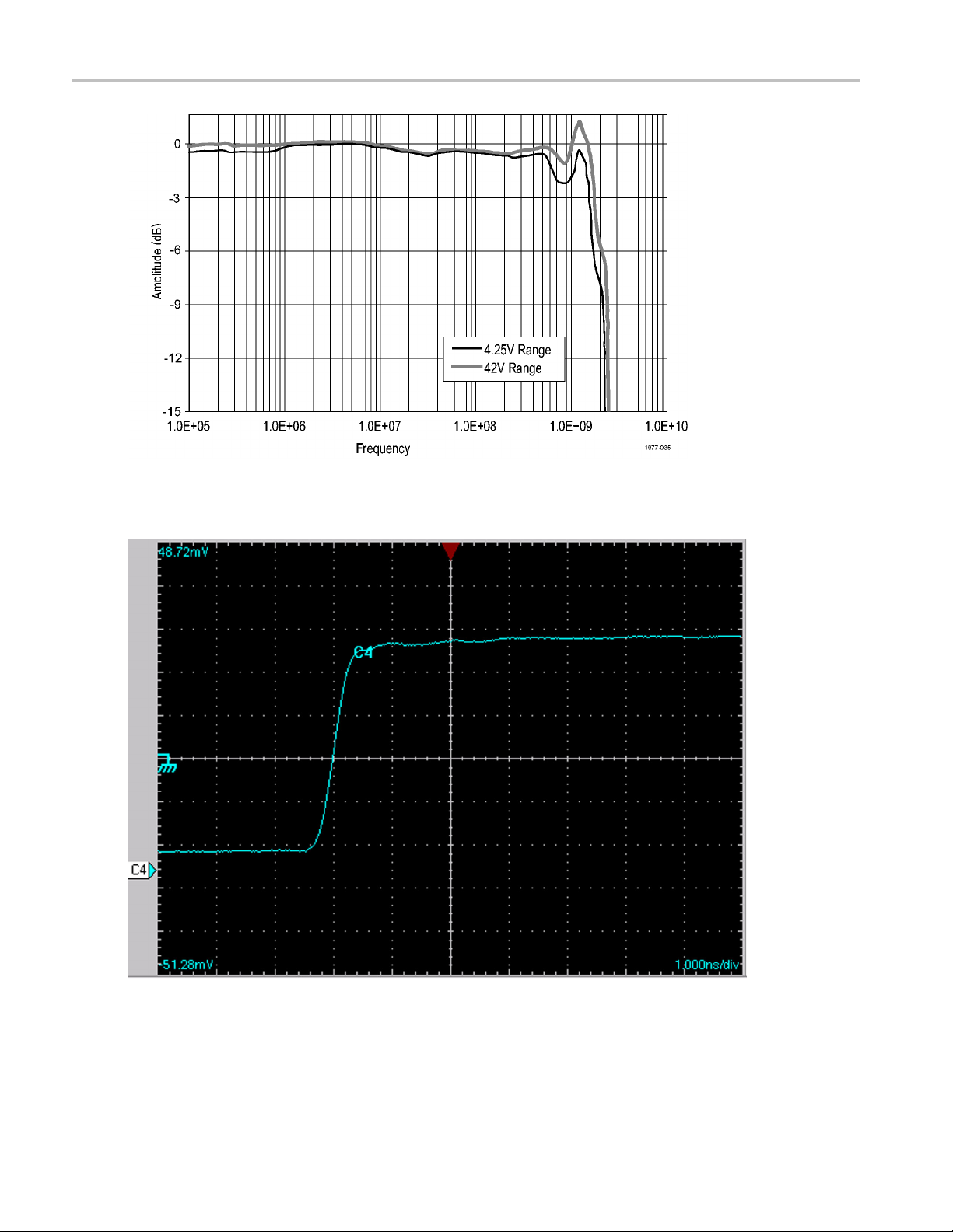
1: Typical bandwidth (P6250)
Figure
P6250 & P6251 Technical Reference 3
Typical Charact
Figure 2: Typical bandwidth (P6251)
eristics
Figure 3: Typical rise time (P6250)
4 P6250 & P6251 Technical Reference
Typical Charact
eristics
Figure 4: Typical rise time (P6251)
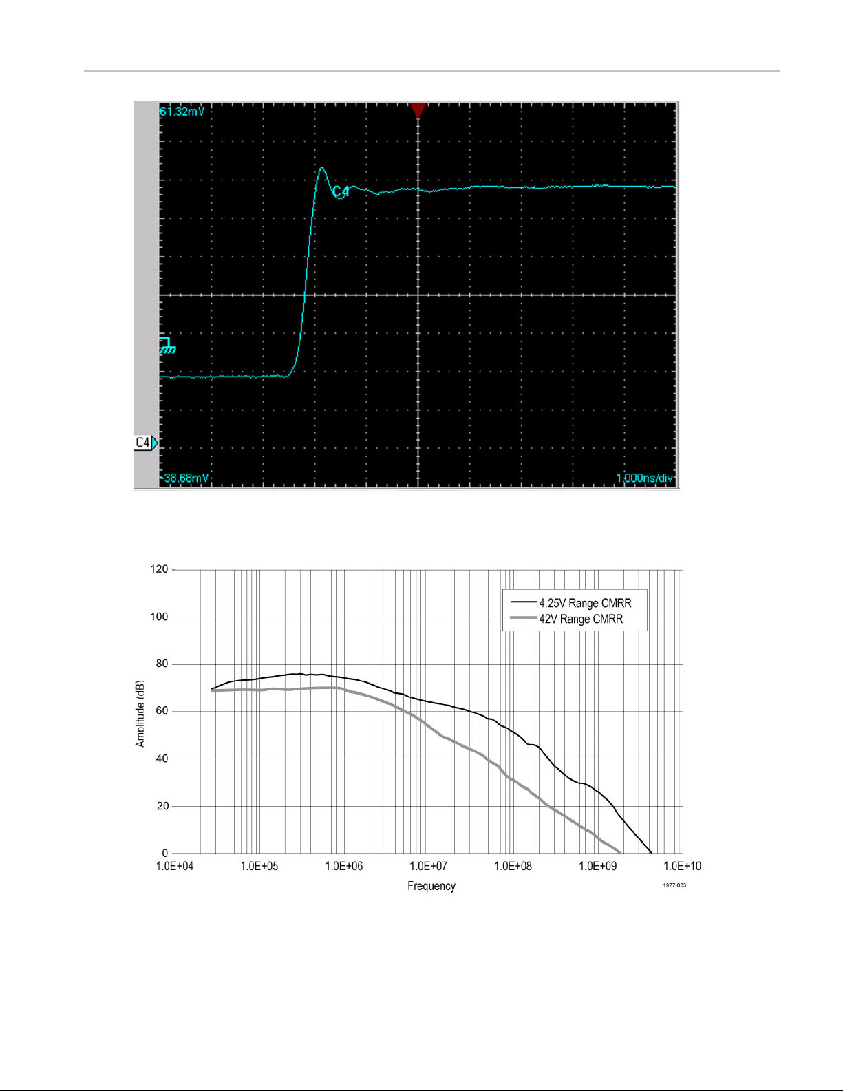
Figure 5: Typical Common-Mode Rejection Ratio (P6250)
P6250 & P6251 Technical Reference 5
Typical Charact
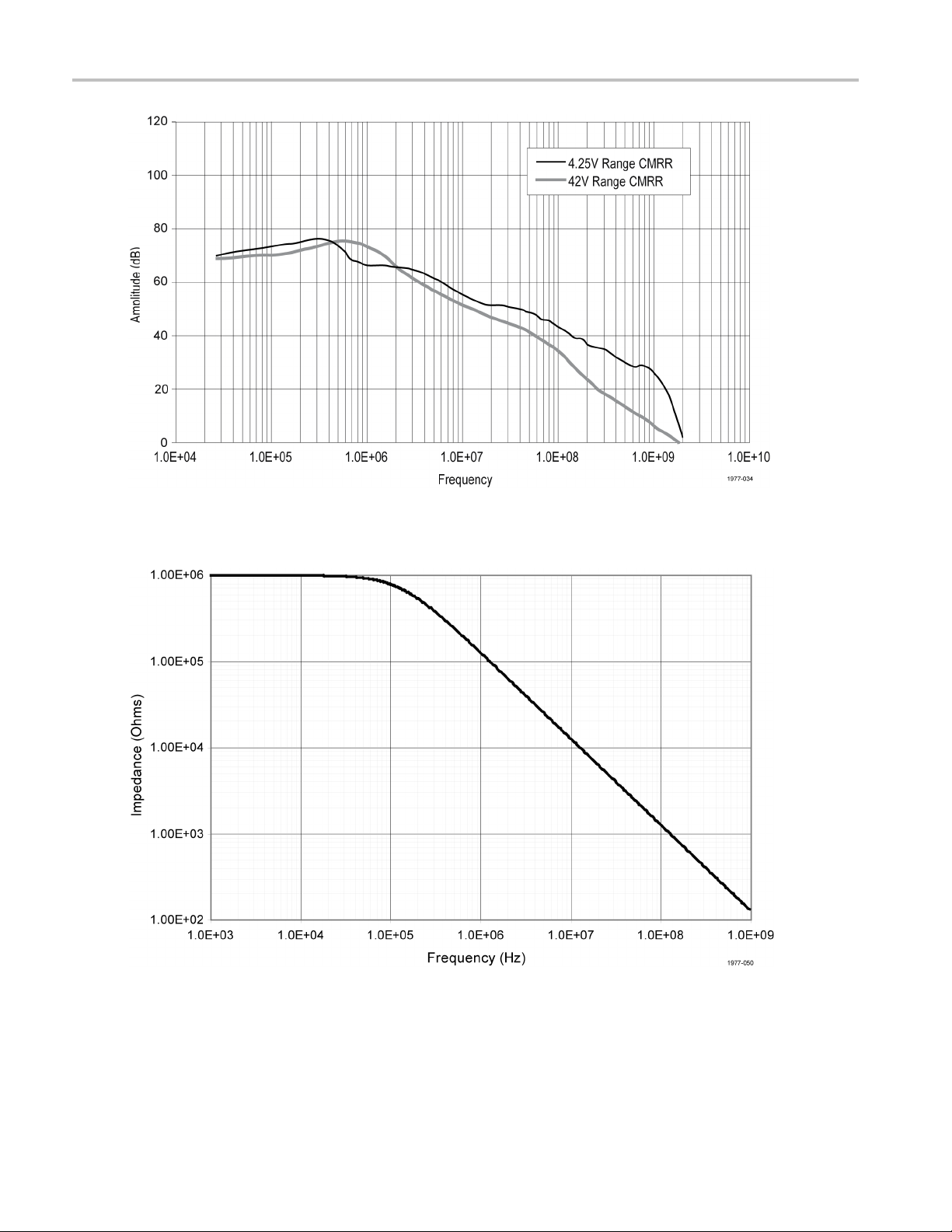
Figure 6: Typical Common-Mode Rejection Ratio (P6251)
eristics
Figure 7: Typical input impedance versus frequency
6 P6250 & P6251 Technical Reference

Table 3: Typical mechanical characteristics
Typical Charact
eristics
Dimensions, input connection
Dimensions, control box
Dimensions, probe head
Dimensions, output cable
Unit weight (p
robe only)
0.63 mm (0.025 i
82 mm × 41 mm × 26
86 mm × 11 mm × 6.
1.22 m (48 in)
163 g (5.24 oz)
n) square pin on 2.54 mm (0.100 in) centers
mm (3.2 in × 1.6 in × 1 .0 in)
3mm(3.4in×0.45in×0.25in)
P6250 & P6251 Technical Reference 7

Nominal Charact
eristics
Nominal Chara
Nominal characteristics (Table 4) describe guaranteed traits, but the traits do not have tolerance limits.
Table 4: Nominal electrical characteristics
Input configuration Differential (two inputs, + and - ), with case ground
Output coupling DC coupling
Voltage ranges 4.25 V and 42 V
Termination
cteristics
Terminate output into 50 Ω
8 P6250 & P6251 Technical Reference

Probe Tip Adapte
r Specifications
Probe Tip Adap
This section describes the characteristics of the adapters that are included in your accessory kit. The adapters are listed
in order of performance, beginning with the fastest. You will obtain the best probe performance by connecting the probe
directly to square pins on your circuit. However, as test points are not always as convenient, these adapters m ake taking
measurements easier while maintaining the best signal fidelity.
NOTE. All adapter specifications are typical unless otherwise indicated.
Straight Pins
Tektr o nix p a
Bandwidth: >
10/90 Rise ti
Best overall
rt number: 016-1891-xx
1.0 GHz
me: <350 ps
signal fidelity of the available adapters.
ter Specifications
P6250 & P6251 Technical Reference 9

Probe Tip Adapte
Longhorn Adapter
Tektronix part number: 016-1780-xx
Bandwidth: >1.0 GHz
10/90 Rise time: <350 ps
This adapter has sharp, adjustable pins that can span up to 0.35 inch apart. They are useful for probing small circuit
board features such as vias and narrow traces.
rSpecifications
10 P6250 & P6251 Technical Reference
 Loading...