

Tektronix P6245 Instruction Manual

Instruction Manual
P6245
1.5 GHz 10X Active Probe
070-8995-04
www.tektronix.com

Copyright © Tektronix, Inc. All rights reserved.
Tektronix products are covered by U.S. and foreign patents, issued and
pending. Information in this publication supercedes that in a ll previously
published material. Specifications and price change privileges reserved.
Tektronix, Inc., P.O. Box 500, Beaverton, OR 97077
TEKTRONIX and TEK are registered trademarks of Tektronix, Inc.

WARRANTY
Tektronix warrants that the systems that it manufactures and sells, (excluding
customer-supplied equipment), will be free from defects in materials and workmanship for
a period of one (1) year. The warranty period shall begin on the date of installation or one
(1) month after the date of shipment, whichever is earlier. If any component of a system
supplied by Tektronix proves defective during the initial one-year period, Tektronix, at its
option, either will repair the defective component without charge for parts and labor, or
will provide a replacement in exchange for the defective component. If any component of
the system is a Tektronix product that is normally sold with a separate warranty, such
separate warranty will apply to the component whenever its terms are more favorable to
the Customer.
In order to obtain service under this warranty, Customer must notify Tektronix of the
defect before the expiration of the respective warranty period and make suitable
arrangements for the performance of service. T ektronix will provide such service at
Customer’s site without charge during the warranty period, if the service is performed
within the normal on-site service area. Tektronix will provide on-site service outside the
normal on-site service area only upon prior agreement and subject to payment of all travel
expenses by Customer. When or where on-site service is not available, Customer shall be
responsible for packaging and shipping the defective component to the service center
designated by Tektronix, with shipping charges prepaid. Tektronix shall pay for the return
of the component to Customer if the shipment is to a location within the country in which
the Tektronix service center is located. Customer shall be responsible for paying all
shipping charges, duties, taxes, and any other charges for components returned to any other
locations.
This warranty shall not apply to any defect, failure, or damage caused by improper use or
improper or inadequate maintenance and care. Tektronix shall not be obligated to furnish
service under this warranty a) to repair damage resulting from attempts by personnel other
than Tektronix representatives to install, repair, or service the system; b) to repair damage
resulting from improper use or connection to incompatible equipment; c) to repair any
damage or malfunction caused by the use of non-Tektronix supplies; or d) to service a
system that has been modified or integrated with other products when the effect of such
modification or integration increases the time or difficulty of servicing the system.
THIS WARRANTY IS GIVEN BY TEKTRONIX WITH RESPECT TO THE
LISTED SYSTEMS IN LIEU OF ANY OTHER WARRANTIES, EXPRESS OR
IMPLIED. TEKTRONIX AND ITS VENDORS DISCLAIM ANY IMPLIED
WARRANTIES OF MERCHANTABILITY OR FITNESS FOR A PARTICULAR
PURPOSE. TEKTRONIX’ RESPONSIBILITY TO REPAIR OR REPLACE
DEFECTIVE PRODUCTS IS THE SOLE AND EXCLUSIVE REMEDY
PROVIDED TO THE CUSTOMER FOR BREACH OF THIS WARRANTY.
TEKTRONIX AND ITS VENDORS WILL NOT BE LIABLE FOR ANY
INDIRECT, SPECIAL, INCIDENTAL, OR CONSEQUENTIAL DAMAGES
IRRESPECTIVE OF WHETHER TEKTRONIX OR THE VENDOR HAS
ADVANCE NOTICE OF THE POSSIBILITY OF SUCH DAMAGES.


Table of Contents
Getting Started
Product Description 1--1.................................
Standard Accessories 1 --1.................................
Customer Support 1--2...................................
Features and Accessories 1--3.............................
Configuration 1--7......................................
Probe Offset 1--7........................................
Functional Check 1--9...................................
Operating Basics
Operating Basics 2--1...................................
Maximum Non-destructive Input Voltage 2--1.................
Input Linear Dynamic Range 2--1..........................
Ground Lead Length 2--2.................................
Helpful Hints 2--5......................................
Low-inductance Grounding 2--5............................
SureFoot Grounding 2--6................................
Probe Tip Test Points 2--7.................................
Probe Tip Stabilization 2--8...............................
Specifications
P6245 Instruction Manual
i

Table of Contents
List of Figures
Figure 1-- 1: Dynamic and Offset Limitations 1--8..............
Figure 1--2: Probe Functional Check Connections 1--9..........
Figure 2--1: Waveform Distortion from Ground Lead L ength 2--2.
Figure 2--2: Ground Lead Equivalent Circuit 2--3..............
Figure 2--3: Low-inductance Grounding 2--5..................
Figure 2--4: Using a SureFoot Adapter for Grounding 2--6.......
Figure 2--5: Using a Probe Tip as a Test Point 2--7.............
Figure 2-- 6: Probe Tip Stabilizing Notch 2--8.................
Figure 3--1: Typical Bandwidth 3--3.........................
Figure 3--2: Typical Voltage Derating vs. Frequency 3--3........
Figure 3--3: Typical Linearity Error vs VIN 3--4...............
Figure 3--4: Typical Input Impedance vs. Frequency 3--4........
Figure 3--5: Typical Phase vs. Frequency 3--5.................
ii
P6245 Instruction Manual

General Safety Summary
Review the following safety precautions to avoid injury and prevent
damage to this product or any products connected t o it .
Only qualified personnel should perform service procedures.
Injury Precautions
Avoid Electric Overload
To avoid electric shock or fire hazard, do not apply a voltage to a
terminal that is outside the range specified for that terminal.
Do Not Operate Without Covers
To avoid electric shock or fire hazard, do not operat e this product
with covers or panels removed.
Do Not Operate in Wet/Damp Conditions
To avoid electric shock, do not operate this produc t in wet or damp
conditions.
Do Not Operate in Explosive Atmosphere
To avoid injury or fire hazard, do not operate this product in an
explosive atmosphere.
P6245 Instruction Manual
iii
General Safety Summary
Product D amage Precautions
Do Not Operate With Suspected Failures
If you suspect there is damage to this product, have it inspected by
qualified service personnel.
Do Not Immerse in Liquids
Clean the probe using only a damp cloth. Refer to cleaning
instructions.
Safety Terms and Symbols
Terms in This Manual
These terms may appear in this manual:
WARNING. Warning statements identify conditions or practic es that
could result in injury or loss of life.
CAUTION. Caution statements identify conditions or practices that
could result in damage to this product or other property.
iv
P6245 Instruction Manual

Manual Organization
User Information
This section contains the information necessary to install and use the
P6245.
H Getting Started
This section contains the product description, description of
accessories, probe setup configuration, and how to check the probe
for normal operation.
H Operating Basics
This section contains basic information and operating suggesti ons for
optimal probe performance
H Specifications
Service Information
This section contains the information necessary to maintain and
service the P6245.
H Theory of Operation
H Performance Verification
H Adjustments
H Maintenance
H Troubleshooting
Replaceable Parts List
P6245 Instruction Manual
v

Manual Organization
vi
P6245 Instruction Manual

Getting Started


Product Description
The Tektronix P6245 is a 1. 5 GHz (probe only), 10X active FET
probe with less than 1 pF input capacitance. The P6245’s low input
capacitance and high input resistance minimize circuit loading over a
wide bandwidth range. The P6245’s small profile and low-mass head
makes probing crowded circuits by hand fast and easy. The accessory
tips and adapters enable the P6245 to be used on a wide variety of
circuit architectures.
The P6245 is powered t hrough a TEKPROBE interface between the
probe’s compensation box and the oscilloscope. The P6245 may be
used with non-TEKPROBE oscilloscopes and instruments by using
the optional Tektronix 1103 Probe Power Supply.
In order to fully appreciate the probe’s capabilities, please read the
Getting Started and Operating Basics sections of this manual.
Standard Accessories
The P6245 is shipped wit h the following standa rd accessories:
H standard probe tips
H SMT KlipChip microcircuit test leads
H Y-lead adapter
H right-angle adapter
H signal-ground adapters
H three- and six-inch ground leads
H low-inductance ground lead
H marker rings
H Instruction Manual
For part number information for standard and optional accessories,
refer to the Replaceable Parts section of this manual.
P6245 Instruction Manual
1- 1

Product Description
Customer Support
To help you get the best performance from your probe, Tektronix
offers the following customer support services:
Operational Support
If you need assistance using your probe, please call our Customer
Support Center a t 1-800-TEK-WIDE (1-800-835-9433), extension
2400. If you are outside the United States or Canada, please contact
your nearest Tektronix Service Center.
Service Support
Should your probe need repair that is beyond that supported by this
manual, please contact your nearest Tektronix Service Center.
Sales Support
To order optional equipment and accessories, call the Tektronix
National Marketing Center at 1-800-426-2200. If you are outside the
United States or Canada, please contact your nearest Tektronix
Service Center.
1- 2
P6245 Instruction Manual
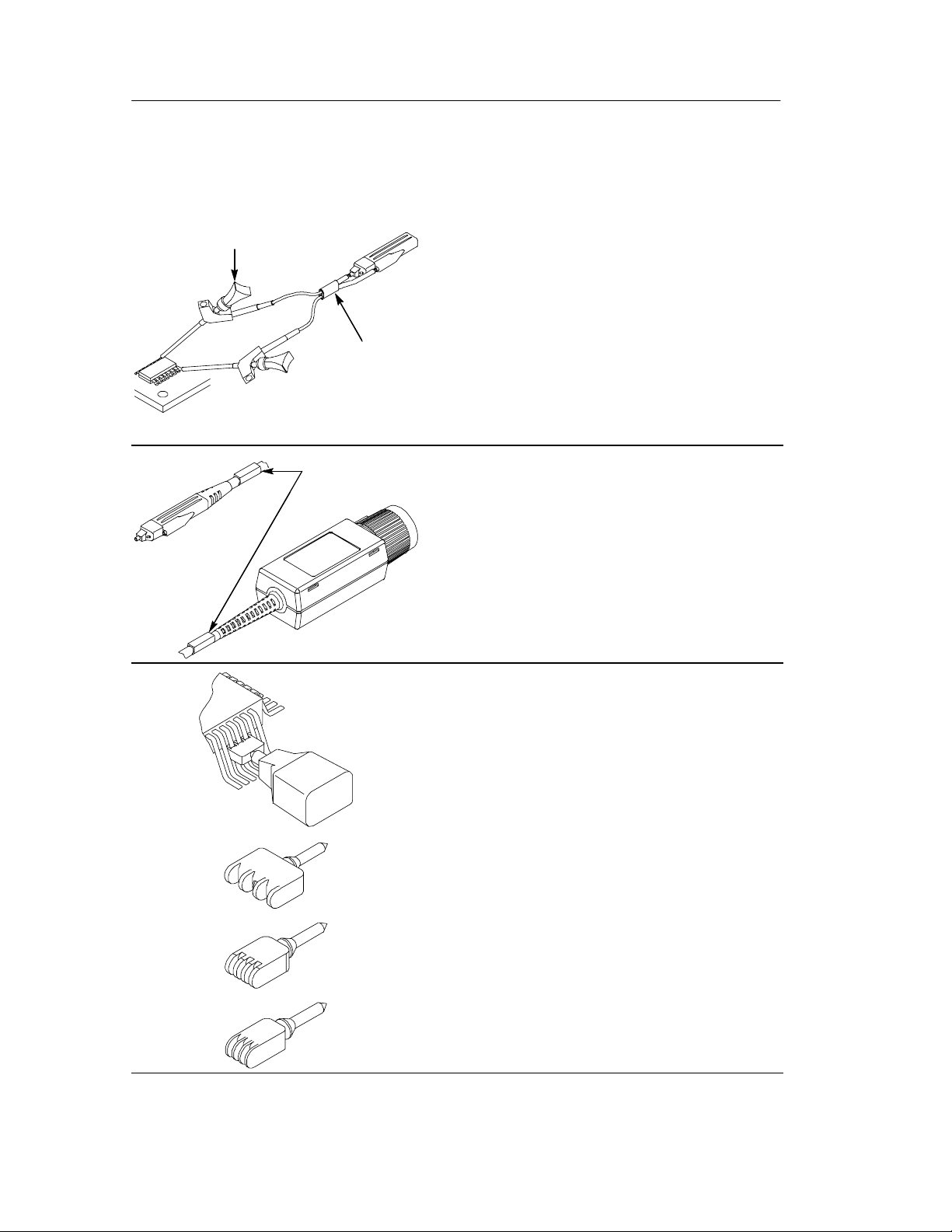
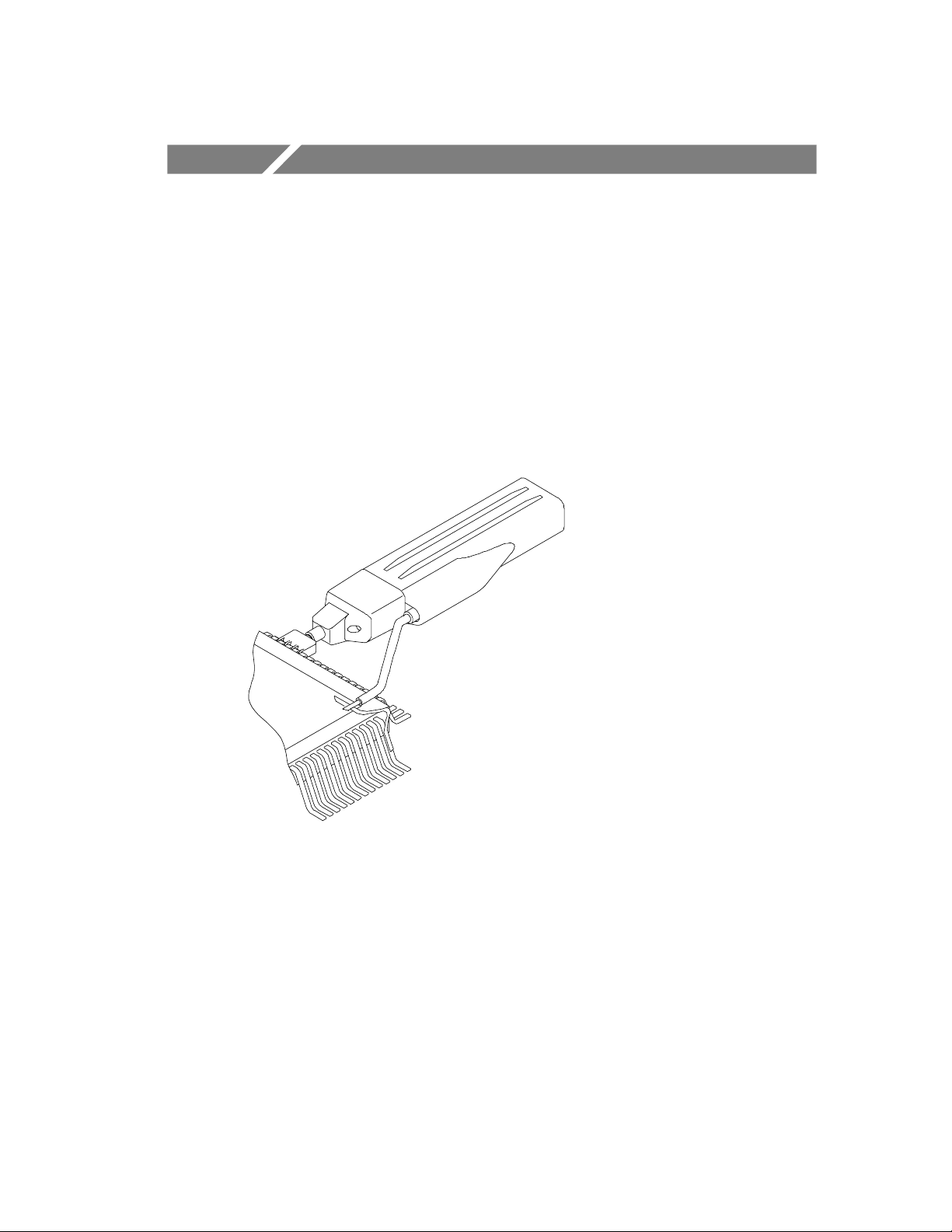
Features and Accessories
The P6245 is provided with several features and accessories designed
to make probing and measurement a simpler task. Please take a
moment to familiarize yourself with these items and their uses.
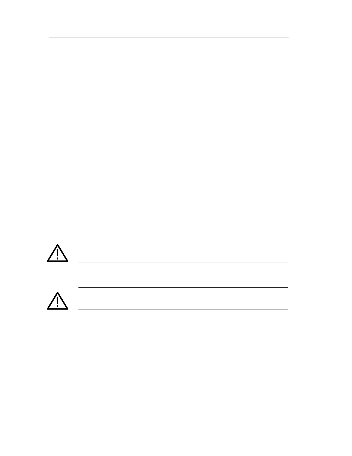
Probe Head Assembly. The probe head is
designed for ease of use and high performance.
Its small size makes it easy to handle in tight
areas.
Probe Tip
Socket
Ground
Socket
Stabilization
Notch
The probe tip socket is sized to easily press onto
0.025 inch pins for direct access. The ground
socket provides a short ground path for high
fidelity ground connections.
The stabilization notch permits you to use
adjacent pins to reduce stresses on the probe
and pins. See pages 1--5 and 2--8 for more
information.
Push-In Probe Tip
TEKPROBE Interface. The TEKPROBE
interface provides a communication path between
the probe and the oscilloscope. Contact pins
provide power, signal, offset, and probe
characteristic data transfer. See page 4--2 for
more information.
If your oscilloscope does not support the
TEKPROBE interface, you can use the optional
1103 probe power supply as an effective
interface. Contact your local Tektronix representative for more information.
Push-in Probe Tip. Use the push-in probe tip
for general purpose probing by hand. The tip may
also be used as a temporary test point. See page
2--7 for more information.
The push-in probe tip may also be used with the
other socketed leads and adapters.
P6245 Instruction Manual
1- 3
Features and Accessories
Installing the Push-in Probe Tip. Attach the
push-in probe tip by seating the tip into the probe
tip socket and pushing the tip in until it is seated.
Either end of the tip may be used.
Do not force the tip. Also, be careful not to poke
yourself with the sharp probe-tip. To remove the
tip, gently grab the tip with small pliers and pull
the tip out.
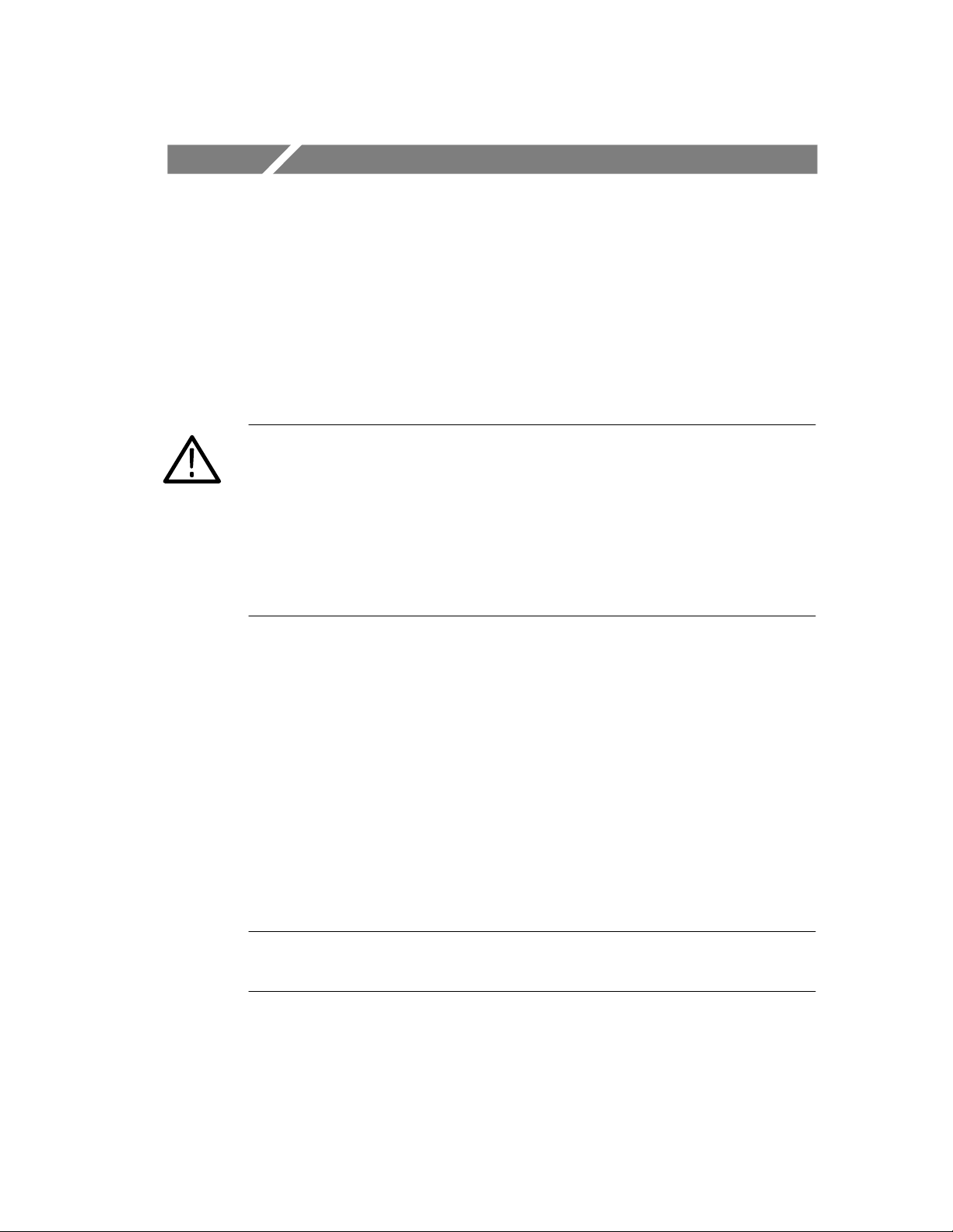
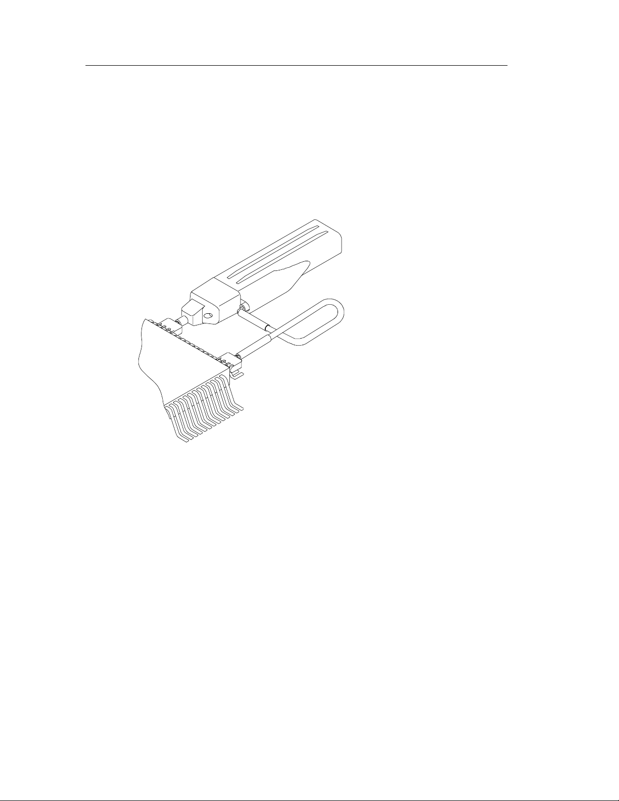
Right-angle adapter. Use the right-angle
adapter for low-profile probing of 0.025 inch
diameter square pins.
The right-angle adapter allows the P6245 to lie
flat against a circuit board. This enables probing
in vertical circuits such as computer or communications backplanes, or in tight areas such as
between circuit cards.
Y-lead
Adapter
Right Angle
Adapter
The right-angle adapter can be used directly with
the probe head, or attached to the Y-lead adapter
or ground leads.
The right-angle adapter is attached the same way
as the push-in probe tip, and can be easily
removed by hand.
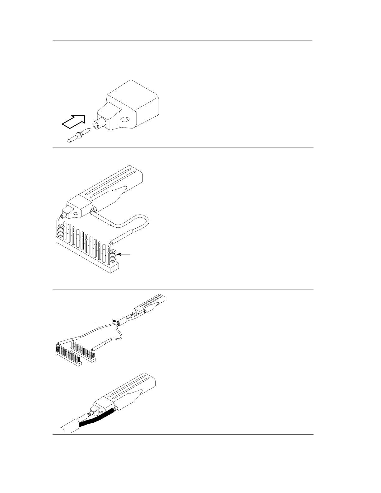
“Y-lead” adapter. Use the Y-lead adapter to
extend the physical reach of the probe and
ground when necessary. The Y-lead adapter
accepts any of the probe tips or adapters, and
can be pushed directly onto 0.025 inch pins.
When selecting the grounding connection,
maintain as short a ground path as possible.
Refer to page 2--2 for more information.
To attach the Y-lead adapter, gently press the
lead pins into the probe head tip and ground
receptacles. Using the black lead for ground is
recommended.
1- 4
P6245 Instruction Manual
Features and Accessories
3 and 6 inch ground l eads. Use the three- and
six-inch ground leads for general probing. The
socketed end of the leads may be connected to
any of the probe tips and adapters, or fitted onto
0.025 inch pins.
To attach the ground leads, press and rotate the
lead pin connector into the ground socket on the
probe head. The lead may be removed by simply
pulling the pin out by hand.
When selecting the grounding connection,
maintain as short a ground path as possible.
Refer to page 2--2 for more information.
Low-inductance ground lead. Use the
low-inductance ground adapter to substantially
reduce ground lead inductance. Because the
ground lead simply touches the ground reference,
you can easily move the probe to different points
on the device under test.
Signal Ground
Adapter
To attach, press the ground lead into the probe
head gound socket.
When selecting the grounding connection,
maintain as short a ground path as possible.
Refer to page 2--2 for more information.
Signal-Ground Adapter. The signal-ground
adapter is ideal for use with signal/ground pairs
on 0.100 inch header pins (such as FlexLead
adapters).
Attach the signal-ground adapter by gently
pressing it into the ground socket on the probe
head.
Be sure to use the stabilization notch whenever
possible. See page 2--8 for further details.
FlexLead
Adapter
P6245 Instruction Manual
1- 5
Features and Accessories
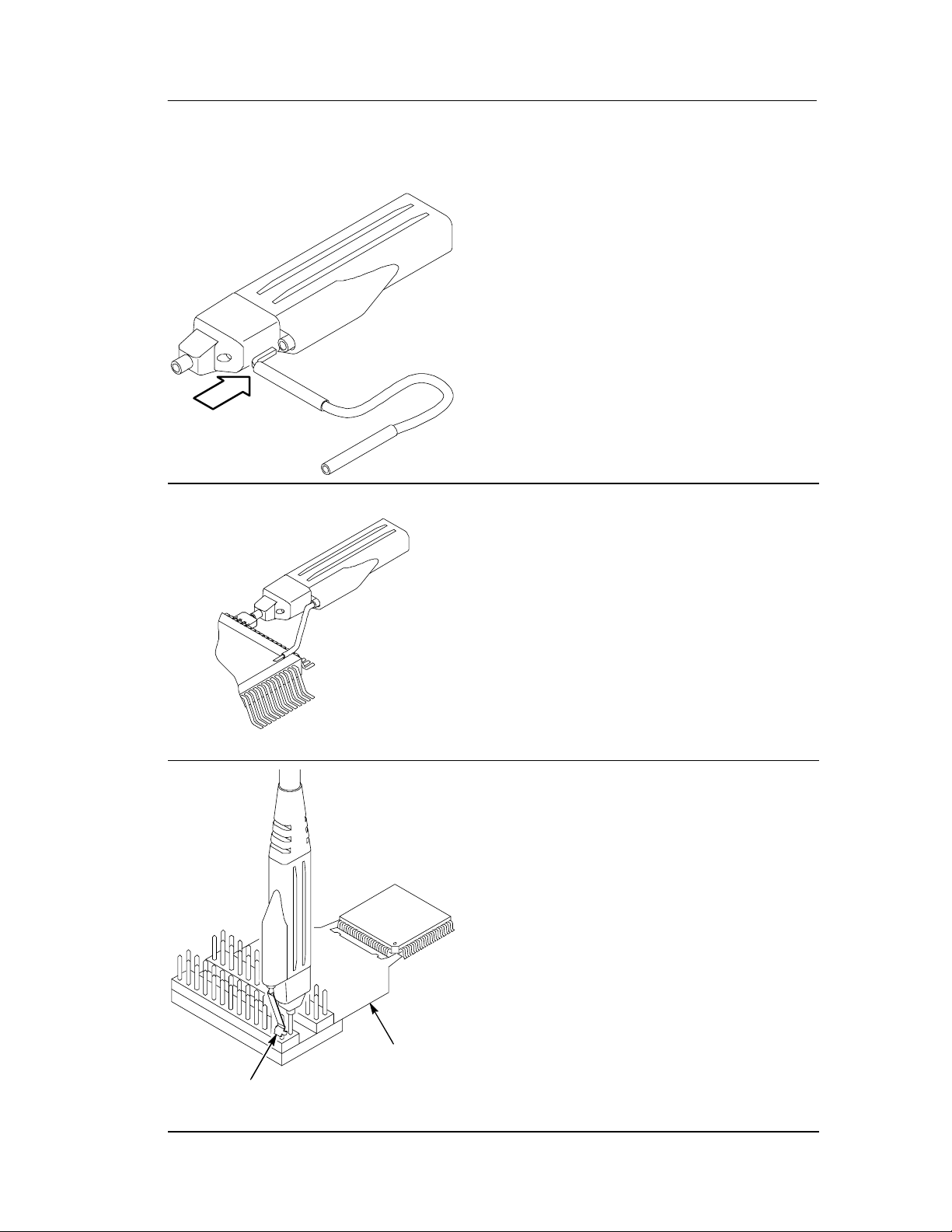
KlipChip
Y-lead
Adapter
SMT KlipChip. Use the SMT KlipChip test
clips to access fragile, dense circuitry.
KlipChip test clips can be connected to the Y-lead
or three- or six-inch ground leads. Simply press
the lead socket into the KlipChip handle.
The KlipChip body freely turns, allowing better
probe orientation. To reduce stress and provide a
lower profile on components being tested, the
flexible sleeve of the KlipChip bends up to a
35 degree angle.
Color Marker
Bands
Color Marker Bands. Attach matching pairs of
the color marker bands onto the cable at the head
and compensation box of each probe. The marker
bands enable quick verification of which probe is
connected to which instrument channel.
SureFoot probe tip (optional). The
SureFoot tip is an integral probe tip and miniature
guide that enables fault-free probing of fine-pitch
SMD packages. Attach the SureFoot adapters the
same way as the push-in probe tips. They can be
used with any of the socketed accessory leads.
The yellow, 0.050 inch SureFoot tip is compatible
with 50 mil JEDEC packages such as SOIC,
PLCC, CLCC, etc.
1- 6
The blue, 0.025 inch SureFoot tip is compatible
with 0.65 mm JEDEC and EIAJ packages.
The red, 0.5 mm SureFoot tip is compatible with
EIAJ packages.
P6245 Instruction Manual
Configuration
The P6245 provides the oscilloscope with the probe model number,
serial number, and attenuation factor. When connected to a
TEKPROBE oscilloscope, display readouts are corrected for the
probe attenuation factor, the instrument input is set to 50 Ω, and the
coupling is set to DC.
CAUTION. Do not attempt to install the P6245 on a non-TEKPROBE
connector. Damage to the probe and connector may result. If your
oscilloscope does not support the TEKPROBE interface, use the
optional Tektronix 1103 Probe Power Supply.
If the P6245 is used with the Tektronix 1103 Probe Power Supply, be
sure to have a 50 Ω termination at the oscilloscope. Also, set the
oscilloscope channel coupling to DC.
The probe offset control is controlled by the oscilloscope. If the
oscilloscope used does not support t he T EKPROBE interface, the
offset controls on the optional Tektronix 1103 Probe Power Supply
can be used.
Probe Offset
The probe offset is adjustable to permit operation within the probe’s
linear range. Using the offset to cancel DC signal component s
enables optimal probe performance. See Figure 1-- 1 on page 1-- 8.
NOTE. See your oscilloscope manual for specific instructions on its
operation and offset control.
P6245 Instruction Manual
1- 7

Configuration
To set the probe offset, follow these steps:
1. Set the oscilloscope coupling to GND.
2. Use the vertical position control to set a zero reference level on
3. Set the oscilloscope coupling to DC and 5 V/div.
4. Attach the probe to the circuit.
5. Adjust the probe offset to bring the trace to the oscilloscope zero
6. Change the volts/division setting to the desired range, adjusting
NOTE.TheP6245 has a ±10 V offset range. The linear operating
range is ±8 V. See Figure 1 --1. Also, see page 2--1 for more
information.
the oscilloscope display.
reference.
the offset to keep the trace on the zero reference level.
If cursors are used on a TEKPROBE oscilloscope, the zero reference
will be at the probe offset voltage.
Nonoperating Range (+15 V Maximum Non-destructive Input Voltage )
+15 V
+10 V
+8 V
0V
-- 8 V
--10 V
--15 V
Nonoperating Range (--15 V Maximum Non-destructive Input Voltage )
Figure 1-1: Dynamic and Offset Limitations
+10 V
Maximum Offset RangeMaximum AC Signal Amplitude
--10 V
1- 8
P6245 Instruction Manual
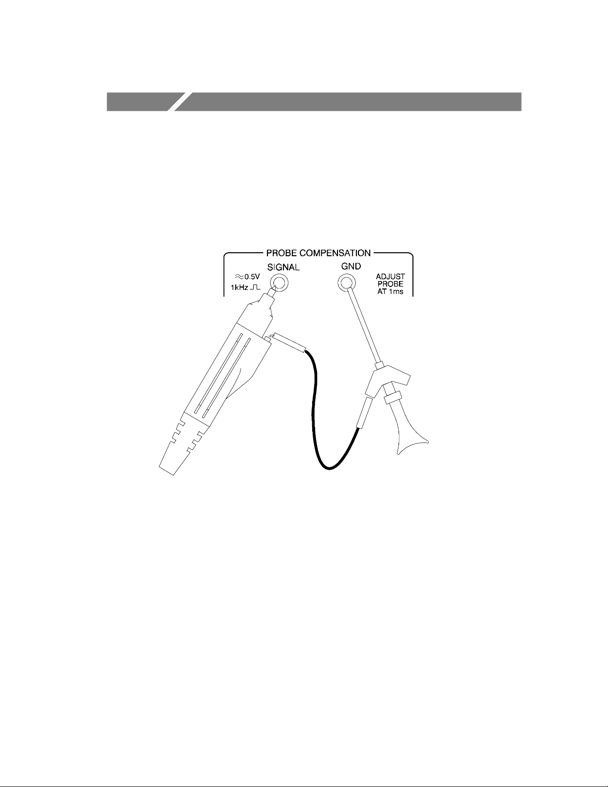
Functional Check
After installing the probe on the oscilloscope, a functional check
may be performed using the PROBE COMPENSATION connec-
tions on the front panel of the oscilloscope. See Figure 1--2.
Figure 1-2: Probe Functional Check Connections
1. Connect the probe to the oscilloscope.
2. Set the oscilloscope to display the probe’s channel.
3. Using a ground lead and a SMT KlipChip, connect the probe
ground to the PROBE COMPENSATION ground connection on
the oscilloscope.
4. Using a standard tip, hold the probe to the SIGNAL terminal on
the oscilloscope.
5. Press AUTOSET (or adjust the oscilloscope) to display the
calibration waveform.
P6245 Instruction Manual
1- 9

Functional Check
NOTE. If your instrument supports probe calibration routines, now is
a good time to perform them.
6. Disconnect the probe from the SIGNAL terminal and ground the
probe tip. (Connect the KlipChip to the probe tip.)
7. With the probe offset set to 0.0 V, the oscilloscope display should
be at the ground reference.
8. Set the oscilloscope volts/division to 5 V.
9. Adjust the probe offset. The displayed waveform should vary
between approximately +10 V and --10 V. (A +10 V offset
displays a --10 V level on your instrument.)
NOTE. If no waveform is display ed, check the vertical coupling to be
sure that it is set to DC.
If the offset adjustment has no effect, set the vertical coupling to DC.
If you are using the Tektronix 1103 Probe Power Supply, and the
waveform is distorted, check to make sure that the oscilloscope
termination is 50 Ω.
If the probe does not pa ss this functional check, go to the Troubleshooting section of this manual.
1- 10
P6245 Instruction Manual

Operating Basics


Operating Basics
Please follow these operating guidelines to get optimum performance
from your P6245.
Maximum Non-destructive Input Voltage
The P6245 is electrically protected against static voltage; however,
applying voltages above its design limits may damage the probe tip
amplifier. Please refer to the Specifications section of thi s manua l for
the maximum operating voltage and frequency dera ting information.
Input Linear Dynamic Range
The probe head a mplifier used by the P6245 has a limited linear
operating range. To keep the input linearity error less than 4% you
must limit the signal input voltage to ±8 V (including any DC offset).
Use the DC offset adjustment to maintain the probe within its
dynamic range. The nominal offset adjustment range of the P6245 is
±10 VDC. For exam ple: to offset a +5 VDC level in a circuit, set the
offset to +5 V.
P6245 Instruction Manual
2- 1
Operating Basics
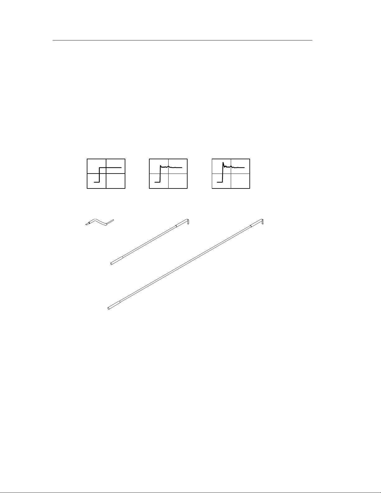
Ground Lead Length
When you are probing a circuit, you should always use as short a
ground lead as possible between the probe head and circuit ground.
The series inductance added by the probe tip and ground lead can
result in a resonant circuit; this circuit may cause parasitic “ringing”
within the bandwidth of your oscilloscope. Refer to Figure 2--1.
Low-inductance
Ground
Three-inch
Ground
Six-inch
Ground
Figure 2-1: Waveform Distortion from Ground Lead Length
Ground Lead Inductance
When you touch your probe tip to a circuit element, you are
introducing a new resistance, capacitance, and inductance into the
circuit. Refer to Figure 2--2.
2- 2
P6245 Instruction Manual
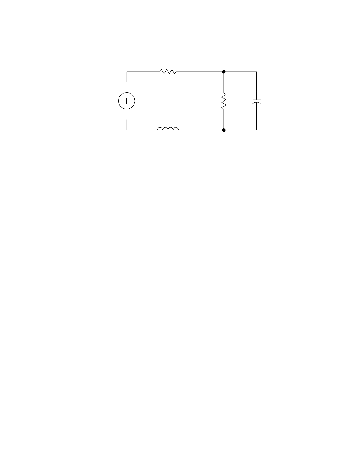
R
Operating Basics
source
V
source
(Ground Lead)
L
gl
Probe R
1MΩ
in
Probe C
1pF
in
Figure 2-2: Ground Lead Equivalent Circuit
Ringing and rise time degradation can be masked if the frequency
content of the signal degradation is beyond the bandwidth of the
oscilloscope.
You can det ermine if ground lead effects may be a problem in your
application if you know the self-inductance (L) and capa citance (C)
of your probe and ground lead. Calculate the approximate resonant
frequency (f
) at which this parasitic circuit will resonate with the
0
following formula:
=
f
0
1
2π LC
The preceding equation shows t hat reducing the ground lead
inductance will raise the resonant frequency. If your measurements
are affected by ringing, your goal is to lower the inductance of your
ground path until the resulting resonant frequency is well above the
frequency of your measurements.
The low-inductance ground contacts described in Accessories can
help you reduce the e ffects of ground lead inductance on your
measurements.
P6245 Instruction Manual
2- 3

Operating Basics
2- 4
P6245 Instruction Manual
Helpful Hints
Follow these helpful hints to make probing easier and noise free.
Low-inductance Grounding
Placing a ground plane on top of a package being probed ca n
minimize ground lead length and inductance. See Figure 2--3.
Figure 2-3: Low-inductance Grounding
Attach a small piece of copper clad on top of the package and
connect it to the package ground connection. Use the low-inductance
ground lead provided with the P6245 to keep the ground lead length
as short as possible.
This method is very useful when making many measurements on the
same package. Using a ground plane on the package makes probing
the package easier, and a voids adding unnecessary ground lead
length and distortion.
P6245 Instruction Manual
2- 5
Helpful Hints
SureFoot Grounding
If you cannot use the low-inductance groundi ng method recommended, the probe may be grounded to the package under test using
a SureFoot adapter. Refer to Figure 2--4.
Figure 2-4: Using a SureFoot Adapter for Grounding
Use a SureFoot a dapter at the end of a short ground lead to connect
directly to the package ground. This method is preferred over using
an adjacent circuit ground because it is the shortest ground path
possible.
2- 6
P6245 Instruction Manual
 Loading...