

Page 1

Instruction Manual
P6205
FET Probe
070-8202-01
Warning
The servicing instructions are for use by qualified
personnel only. To avoid personal injury, do not
perform any servicing unless you are qualified to
do so. Refer to all safety summaries prior to
performing service.
Page 2

Copyright Tektronix, Inc. All rights reserved.
Tektronix products are covered by U.S. and foreign patents, issued and
pending. Information in this publication supercedes that in all previously
published material. Specifications and price change privileges reserved.
Printed in the U.S.A.
Tektronix, Inc., P.O. Box 1000, Wilsonville, OR 97070–1000
TEKTRONIX, TEK, and TEKPROBE are registered trademarks
of Tektronix, Inc.
KLIPCHIP is a trademark of Tektronix, Inc.
Page 3

WARRANTY
T ektronix warrants that the products that it manufactures and sells will be free from defects
in materials and workmanship for a period of one (1) year from the date of purchase from
an authorized Tektronix distributor. If any such product proves defective during this
warranty period, Tektronix, at its option, either will repair the defective product without
charge for parts and labor, or will provide a replacement in exchange for the defective
product. Batteries are excluded from this warranty.
In order to obtain service under this warranty , Customer must notify T ektronix of the defect
before the expiration of the warranty period and make suitable arrangements for the
performance of service. Customer shall be responsible for packaging and shipping the
defective product to the service center designated by Tektronix, shipping charges prepaid,
and with a copy of customer proof of purchase. Tektronix shall pay for the return of the
product to Customer if the shipment is to a location within the country in which the
Tektronix service center is located. Customer shall be responsible for paying all shipping
charges, duties, taxes, and any other charges for products returned to any other locations.
This warranty shall not apply to any defect, failure or damage caused by improper use or
improper or inadequate maintenance and care. Tektronix shall not be obligated to furnish
service under this warranty a) to repair damage resulting from attempts by personnel other
than Tektronix representatives to install, repair or service the product; b) to repair damage
resulting from improper use or connection to incompatible equipment; c) to repair any
damage or malfunction caused by the use of non-Tektronix supplies; or d) to service a
product that has been modified or integrated with other products when the effect of such
modification or integration increases the time or difficulty of servicing the product.
THIS WARRANTY IS GIVEN BY TEKTRONIX WITH RESPECT TO THE
LISTED PRODUCTS IN LIEU OF ANY OTHER WARRANTIES, EXPRESS OR
IMPLIED. TEKTRONIX AND ITS VENDORS DISCLAIM ANY IMPLIED
WARRANTIES OF MERCHANTABILITY OR FITNESS FOR A PARTICULAR
PURPOSE. TEKTRONIX’ RESPONSIBILITY TO REPAIR OR REPLACE
DEFECTIVE PRODUCTS IS THE SOLE AND EXCLUSIVE REMEDY
PROVIDED TO THE CUSTOMER FOR BREACH OF THIS WARRANTY.
TEKTRONIX AND ITS VENDORS WILL NOT BE LIABLE FOR ANY
INDIRECT, SPECIAL, INCIDENTAL, OR CONSEQUENTIAL DAMAGES
IRRESPECTIVE OF WHETHER TEKTRONIX OR THE VENDOR HAS
ADVANCE NOTICE OF THE POSSIBILITY OF SUCH DAMAGES.
Page 4

Page 5

Table of Contents
General Safety Summary v. . . . . . . . . . . . . . . . . . . . . . . . . . . .
Service Safety Summary vii. . . . . . . . . . . . . . . . . . . . . . . . . . . . .
Preface ix. . . . . . . . . . . . . . . . . . . . . . . . . . . . . . . . . . . . . . . . . . . .
Contacting Tektronix x. . . . . . . . . . . . . . . . . . . . . . . . . . . . . . . . .
Getting Started
Product Description 1–1. . . . . . . . . . . . . . . . . . . . . . . . . . . . . . . . . .
Oscilloscopes without the TEKPROBE Interface 1–1. . . . . . . .
Standard Accessories 1–3. . . . . . . . . . . . . . . . . . . . . . . . . . . . . . . . .
Probe Features 1–3. . . . . . . . . . . . . . . . . . . . . . . . . . . . . . . . . . . . . .
Grounding the Probe 1–7. . . . . . . . . . . . . . . . . . . . . . . . . . . . . . . . .
Operating Basics
Ground Lead Inductance 2–1. . . . . . . . . . . . . . . . . . . . . . . . . . . . . .
Linear Operating Range 2–3. . . . . . . . . . . . . . . . . . . . . . . . . . . . . . .
High-Amplitude Frequency Response 2–3. . . . . . . . . . . . . . . . . . . .
Step Inputs 2–3. . . . . . . . . . . . . . . . . . . . . . . . . . . . . . . . . . . . . .
Sine Wave Inputs 2–5. . . . . . . . . . . . . . . . . . . . . . . . . . . . . . . . .
Specifications
Performance Verification
Test Equipment 4–1. . . . . . . . . . . . . . . . . . . . . . . . . . . . . . . . . . . . .
Attenuation Check 4–2. . . . . . . . . . . . . . . . . . . . . . . . . . . . . . . . . . .
Rise Time Check 4–5. . . . . . . . . . . . . . . . . . . . . . . . . . . . . . . . . . . .
Rise Time Approximation 4–7. . . . . . . . . . . . . . . . . . . . . . . . . .
Bandwidth Approximation 4–8. . . . . . . . . . . . . . . . . . . . . . . . . .
Aberrations Check 4–9. . . . . . . . . . . . . . . . . . . . . . . . . . . . . . . . . . .
Output Offset Check 4–14. . . . . . . . . . . . . . . . . . . . . . . . . . . . . . . . .
P6205 Instruction Manual
i
Page 6

Table of Contents
Maintenance
Preventive Maintenance 5–1. . . . . . . . . . . . . . . . . . . . . . . . . . . . . . .
V isual Inspection 5–1. . . . . . . . . . . . . . . . . . . . . . . . . . . . . . . . .
Cleaning 5–2. . . . . . . . . . . . . . . . . . . . . . . . . . . . . . . . . . . . . . . .
Corrective Maintenance 5–2. . . . . . . . . . . . . . . . . . . . . . . . . . . . . . .
Static Sensitive Devices 5–3. . . . . . . . . . . . . . . . . . . . . . . . . . . .
Replacing the Probe Tip 5–3. . . . . . . . . . . . . . . . . . . . . . . . . . . .
Replacing the TEKPROBE Contact Pins 5–3. . . . . . . . . . . . . .
Replacing Internal Assemblies: Probe Head and Cable,
BNC and Circuit Board Carrier 5–4. . . . . . . . . . . . . . . . . . .
Readjustment Following Repair 5–6. . . . . . . . . . . . . . . . . . . . .
Repackaging for Shipment 5–6. . . . . . . . . . . . . . . . . . . . . . . . . . . .
Replaceable Parts
Parts Ordering Information 6–1. . . . . . . . . . . . . . . . . . . . . . . . . . . .
Module Servicing 6–1. . . . . . . . . . . . . . . . . . . . . . . . . . . . . . . . .
Using the Replaceable Parts List 6–2. . . . . . . . . . . . . . . . . . . . . . . .
Abbreviations 6–3. . . . . . . . . . . . . . . . . . . . . . . . . . . . . . . . . . . .
Mfr . Code to Manufacturer Cross Index 6–3. . . . . . . . . . . . . . .
ii
P6205 Instruction Manual
Page 7

List of Figures
Figure 1–1: P6205 probe with accessories 1–2. . . . . . . . . . . . . . .
Figure 1–2: Probe finger guard and hand contact ar ea 1–7. . . .
Figure 2–1: Equivalent circuit showing added pr obe and
ground lead resistance, capacitance, and inductance 2–1. . .
Figure 2–2: Effects of ground lead inductance on waveform
fidelity 2–2. . . . . . . . . . . . . . . . . . . . . . . . . . . . . . . . . . . . . . . . .
Figure 2–3: P6205 typical input vs linear operating range 2–4.
Figure 2–4: Bandwidth vs sine wave input amplitude 2–5. . . . .
Table of Contents
Figure 3–1: Typical input impedance vs frequency 3–5. . . . . . .
Figure 3–2: Voltage derating vs frequency 3–5. . . . . . . . . . . . . .
Figure 3–3: Linearity error vs output voltage 3–6. . . . . . . . . . . .
Figure 3–4: Typical frequency response 3–6. . . . . . . . . . . . . . . .
Figure 4–1: Attenuation test setup part 1 4–3. . . . . . . . . . . . . . .
Figure 4–2: Calibrator waveform 4–4. . . . . . . . . . . . . . . . . . . . .
Figure 4–3: Cursors placement for D voltage measurement 4–4
Figure 4–4: Attenuation test setup part 2 4–5. . . . . . . . . . . . . . .
Figure 4–5: Rise time test setup 4–6. . . . . . . . . . . . . . . . . . . . . . .
Figure 4–6: Rise time waveform 4–7. . . . . . . . . . . . . . . . . . . . . . .
Figure 4–7: Aberrations test setup part 1 4–9. . . . . . . . . . . . . . .
Figure 4–8: Aberrations waveform 4–10. . . . . . . . . . . . . . . . . . . .
Figure 4–9: Measuring aberrations 4–11. . . . . . . . . . . . . . . . . . . .
Figure 4–10: Aberrations test setup part 2 4–12. . . . . . . . . . . . . .
Figure 5–1: Disassembling the P6205 probe 5–5. . . . . . . . . . . . .
Figure 6–1: P6205 probe with standard accessories 6–4. . . . . . .
Figure 6–2: P6205 probe optional accessories 6–6. . . . . . . . . . . .
P6205 Instruction Manual
iii
Page 8

Table of Contents
List of Tables
Table 1–1: Standard accessories 1–3. . . . . . . . . . . . . . . . . . . . . .
Table 3–1: Electrical characteristics 3–1. . . . . . . . . . . . . . . . . . .
Table 3–2: Environmental characteristics 3–4. . . . . . . . . . . . . .
Table 3–3: Physical characteristics 3–4. . . . . . . . . . . . . . . . . . . .
Table 3–4: Certifications and compliances 3–4. . . . . . . . . . . . . .
Table 4–1: Test equipment 4–2. . . . . . . . . . . . . . . . . . . . . . . . . . .
iv
P6205 Instruction Manual
Page 9

General Safety Summary
Review the following safety precautions to avoid injury and prevent
damage to this product or any products connected to it. To avoid
potential hazards, use this product only as specified.
Only qualified personnel should perform service procedures.
While using this product, you may need to access other parts of the
system. Read the General Safety Summary in other system manuals
for warnings and cautions related to operating the system.
To Avoid Fire or Personal Injury
Connect and Disconnect Properly. Do not connect or disconnect probes
or test leads while they are connected to a voltage source.
Observe All Terminal Ratings. To avoid fire or shock hazard, observe all
ratings and markings on the product. Consult the product manual for
further ratings information before making connections to the product.
Do not apply a potential to any terminal, including the common
terminal, that exceeds the maximum rating of that terminal.
Connect the ground lead of the probe to earth ground only.
Avoid Exposed Circuitry. Do not touch exposed connections and
components when power is present.
Do Not Operate With Suspected Failures. If you suspect there is damage
to this product, have it inspected by qualified service personnel.
Do Not Operate in Wet/Damp Conditions.
Do Not Operate in an Explosive Atmosphere.
Keep Product Surfaces Clean and Dry.
P6205 Instruction Manual
v
Page 10
General Safety Summary
Safety Terms and Symbols
Terms in This Manual. These terms may appear in this manual:
WARNING. Warning statements identify conditions or practices that
could result in injury or loss of life.
CAUTION. Caution statements identify conditions or practices that
could result in damage to this product or other property.
Terms on the Product. These terms may appear on the product:
DANGER indicates an injury hazard immediately accessible as you
read the marking.
WARNING indicates an injury hazard not immediately accessible as
you read the marking.
CAUTION indicates a hazard to property including the product.
Symbols on the Product. These symbols may appear on the product:
WARNING
High Voltage
Protective Ground
(Earth) Terminal
CAUTION
Refer to Manual
Double
Insulated
vi
P6205 Instruction Manual
Page 11

Service Safety Summary
Only qualified personnel should perform service procedures. Read
this Service Safety Summary and the General Safety Summary before
performing any service procedures.
Do Not Service Alone. Do not perform internal service or adjustments
of this product unless another person capable of rendering first aid
and resuscitation is present.
Disconnect Power. To avoid electric shock, disconnect the mains
power by means of the power cord or, if provided, the power switch.
Use Care When Servicing with Power On. Dangerous voltages or currents
may exist in this product. Disconnect power, remove battery (if
applicable), and disconnect test leads before removing protective
panels, soldering, or replacing components.
To avoid electric shock, do not touch exposed connections.
P6205 Instruction Manual
vii
Page 12

Service Safety Summary
viii
P6205 Instruction Manual
Page 13

Preface
This manual provides operating and maintenance information for the
Tektronix P6205 FET probe.
The manual is organized into the following sections:
Getting Started provides a product overview and introduction to
Operating Basics discusses techniques for improving measure-
Specifications lists the probe warranted characteristics.
Performance Verification contains procedures to verify probe
Maintenance contains inspection and cleaning procedures and
Replaceable Parts lists the standard and optional probe parts and
probe features and accessories.
ment accuracy .
performance.
instructions for replacing probe modules.
accessories and provides ordering information.
P6205 Instruction Manual
ix
Page 14

Preface
Contacting Tektronix
Product
Support
Service
Support
For other
information
For application-oriented questions about a Tektronix
measurement product, call toll free in North
America:
1-800-TEK-WIDE (1-800-835-9433 ext. 2400)
6:00 a.m. – 5:00 p.m. Pacific time
Or contact us by e-mail:
tm_app_supp@tek.com
For product support outside of North America,
contact your local Tektronix distributor or sales
office.
Contact your local Tektronix distributor or sales
office. Or visit our web site for a listing of
worldwide service locations.
http://www.tek.com
In North America:
1-800-TEK-WIDE (1-800-835-9433)
An operator will direct your call.
To write us Tektronix, Inc.
P.O. Box 1000
Wilsonville, OR 97070-1000
x
P6205 Instruction Manual
Page 15

Getting Started
Page 16

Page 17

Getting Started
The Tektronix P6205 FET probe is an active 10X-attenuating probe
that is compatible with Tektronix TDS 500 Series, DSA 600 Series,
11000 Series, and CSA 404 oscilloscopes and plug-in units.
Product Description
The P6205 probe provides high-frequency measurement capability
without the capacitive loading and performance limitations inherent
in passive resistive-divider type probes. FETs are used in the P6205
to establish the characteristic high input impedance at high
frequency of an active probe. The P6205 features a 750 MHz
bandwidth with an input impedance of 1 MW in parallel with 2 pF.
You must terminate the P6205 probe output into 50 W.
The P6205 includes the TEKPROBEt Level 2 interface. When used
with a fully TEKPROBE interface-compatible oscilloscope, the
P6205 probe is powered by the host instrument and provides the
oscilloscope with the probe model number, serial number, and
attenuation factor. When installed on a fully compatible oscilloscope, the oscilloscope channel input is automatically set to 50 W
and the display readouts are corrected for the probe attenuation
factor.
Oscilloscopes without the TEKPROBE Interface
The P6205 is an active probe that requires external power to operate.
If your oscilloscope is not equipped with the TEKPROBE interface,
we recommend that you use the Tektronix 1103 TEKPROBE Power
Supply. By connecting the probe to the 1103 power supply, and the
power supply output to your oscilloscope input, you can use the
P6205 probe with oscilloscopes having conventional BNC inputs.
The 1103 can power two P6205 probes simultaneously.
To maintain the best possible high-frequency response with the 1103
power supply, keep the cable connecting the 1103 output to the
oscilloscope input as short as possible. You must use an oscilloscope
with 50 W input impedance with this system.
P6205 Instruction Manual
1–1
Page 18
Getting Started
NOTE. Using the P6205 probe with an 1103 power supply will not
add full TEKPROBE functionality to an incompatible oscilloscope.
In addition, the 1103 probe offset adjustment does not apply to
P6205 probes.
6
7
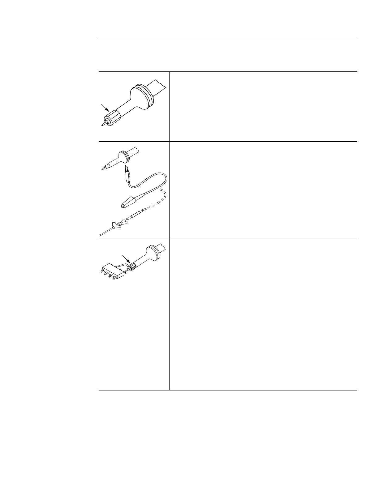
1
3
8
9
2
10
1 Probe head and cable
2 Ground leads
3 Compensation box
4 BNC locking ring
5 TEKPROBE contact pins
5
Figure 1–1: P6205 probe with accessories
4
6 Retractable-hook tip
7 Low-inductance ground tip
8 Ground sleeve tip cover
9 IC protector tip
10 SMT KlipChipt
1–2
P6205 Instruction Manual
Page 19
Standard Accessories
Table 1–1 lists the P6205 probe standard accessories.
T able 1–1: Standard accessories
1 Retractable-hook tip
1 Ground lead with square-pin receptacle
1 Ground lead with alligator clip
1 Ground contact spring
1 Ground sleeve tip cover
1 IC protector tip
1 SMT KlipChip
Getting Started
1 Instruction manual
The Replaceable Parts section beginning on page 6–1, contains
ordering information for all standard and optional accessories.
Probe Features
The following table introduces P6205 probe components, connectors,
and accessories. Refer to Figure 1–1 to identify probe items and
where to attach standard accessories.
Probe Head and Cable. The probe tip makes a physical
connection to the test point. The flexible cable allows you to make
measurements in a variety of applications.
Compensation Box. The compensation box contains circuitry,
including elements of the TEKPROBE interface. There are no
internal adjustments.
P6205 Instruction Manual
1–3
Page 20
Getting Started
Dat
–5 V
Signal
Ground
+5 V
a
Clock
TEKPROBE Interface (Level 2). The TEKPROBE interface
provides a communication path between the probe and the host
instrument. Contact pins provide connections for power, signal,
and data transfer. The interface allows some oscilloscopes to
automatically configure the correct attenuation factor and input
impedance and to access the probe serial number.
Some features of the TEKPROBE interface, for example probe
offset and additional voltage sources, are not required by the
P6205; therefore, the contact pins are omitted from the connector.
NOTE. Your oscilloscope may not implement all features of
the TEKPROBE interface. Refer to your oscilloscope
manual for details.
BNC Locking Ring. The BNC locking ring houses the
TEKPROBE interface contact pins and provides a positive
attachment to the host instrument.
To install the probe, open the locking ring by rotating it
counterclockwise; push the assembly firmly onto the oscilloscope
(or power supply) BNC input connector. Rotate the ring clockwise
one-quarter turn to secure it to the input connector.
Retractable-Hook Tip.1 Attach the retractable-hook tip to your
signal test point for hands-free operation. The hook tip attaches
easily to leaded components such as resistors, capacitors, and
discrete semiconductors. Stripped wire, jumpers, busses, and test
pins can also be gripped with the retractable hook tip.
To remove the hook tip (your probe is shipped with the hook tip
installed), simply pull it off. Reinstall the hook tip by pushing it
firmly onto the molded barrel of the probe tip.
IC Protector Tip.2 Use the IC protector tip to simplify probing of
in-line IC packages. The shape of the protector tip guides the
probe onto IC pins and prevents accidental shorting of pins by the
probe tip.
To install the IC protector tip, push it firmly onto the end of the
metal barrel of the probe tip while taking care not to pierce
yourself with the sharp tip.
NOTE: Remove the IC protector tip by pulling it off before
installing the retractable-hook tip.
1–4
P6205 Instruction Manual
Page 21
Getting Started
Ground Sleeve Tip Cover.2 Use the ground sleeve tip cover to
keep the metal sleeve of the probe tip from accidentally shorting
components on your device under test.
To install the ground sleeve tip cover, push it onto the metal barrel
of the probe tip while taking care not to pierce yourself with the
sharp probe tip. Remove the sleeve by pulling it off before
installing the retractable hook tip.
Ground Leads.1 Use the long ground leads when length is
important and precise high-frequency measurement is not. Long
ground leads are ideal for quick troubleshooting when you are
looking for the presence, absence, or general shape of a signal.
For maximum performance, always use the shortest ground lead
possible.
To attach the ground lead, press the spring clip onto the collar of
the probe head. An alternative ground connection can also be
made to the metal barrel of the probe tip.
Low-Inductance Ground Contact (Spring Tip). Use the
low-inductance spring-tip ground contact to reduce ground lead
inductance. The performance of a probe fitted with the
low-inductance ground contact approaches that of no-lead probe
fixtures and adapters. With the spring-tip contact installed, you
can make measurements up to the system bandwidth of your
probe/oscilloscope with negligible signal degradation from ground
lead inductance.
To install the low-inductance ground contact, push it onto the
metal barrel of the probe tip while taking care not to pierce
yourself with the sharp probe tip.
NOTE: The spring contact installs more easily if you rotate
the spring counterclockwise (loosening the spring tension)
as you push it onto the probe barrel. Use care to avoid the
accidentally shorting of component leads to ground when
using this tip.
P6205 Instruction Manual
1–5
Page 22
Getting Started
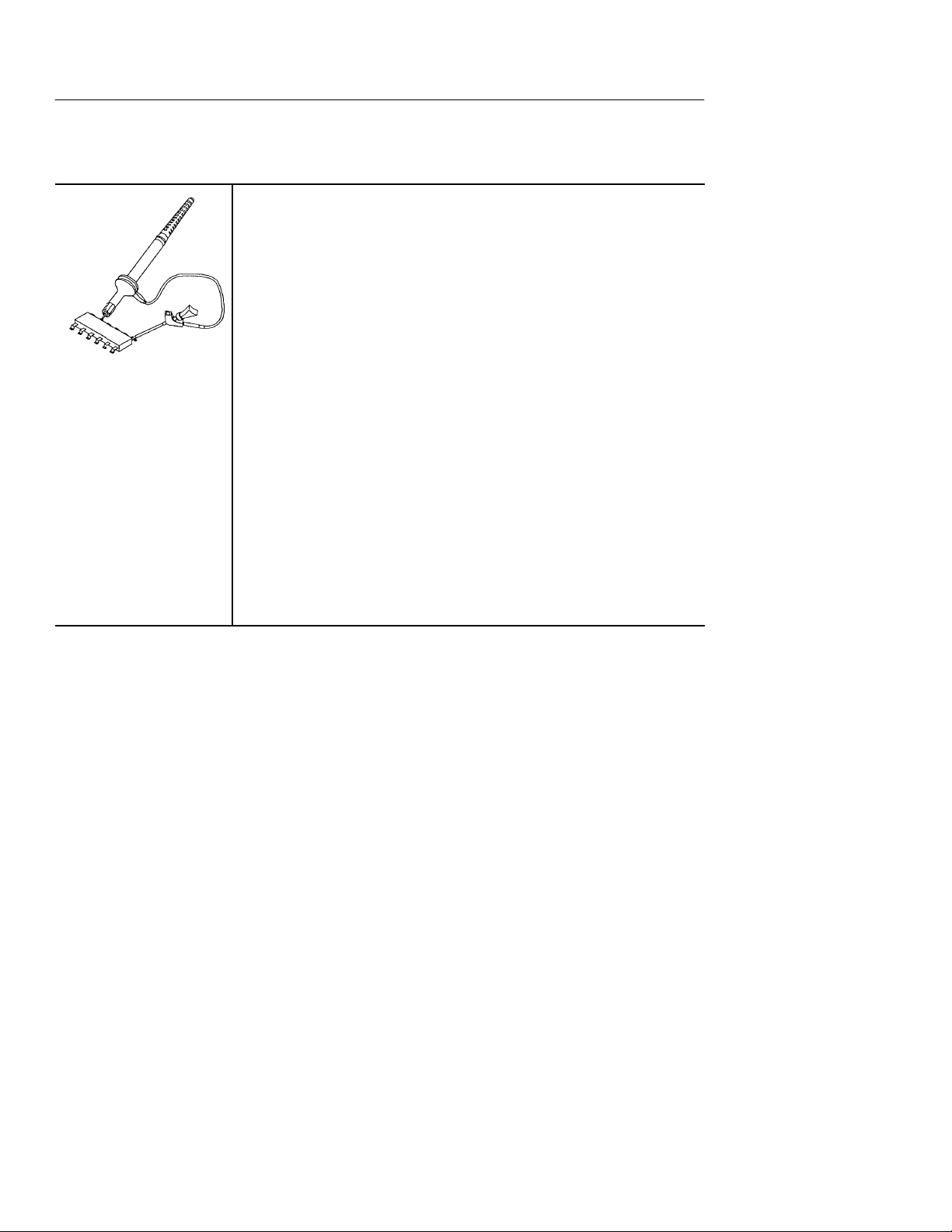
SMT KlipChipt. Use the retractable KlipChip if you need
hands-free attachment to a physically small signal or ground
source. The low profile of the KlipChip allows you to grasp
devices that the Retractable Hook Tip cannot.
To use the KlipChip as a ground connector, attach the long
ground lead with square-pin termination to the probe collar.
Connect the ground lead termination to one of the KlipChip
shoulder pins.
To use the KlipChip as a signal connector, slide the optional
single-lead probe tip adapter (see Replaceable Parts list) onto the
probe tip. Connect the single-lead termination to one of the
KlipChip shoulder pins.
To use the KlipChip as both ground and signal connector, slide
the optional dual-lead probe tip adapter (See Replaceable Parts)
onto the probe tip. Connect both single-lead terminations to the
shoulder of a separate KlipChip pin. You can also combine the
single-lead adapter with a long ground lead to configure dual
KlipChip connections.
1
For maximum flexibility, use one of the six-inch ground leads. For precise
measurements at high frequency, the inductance associated with long ground
leads may distort the high-frequency component of your signal. Consider
whether you can use one of the low-inductance probe tip configurations
instead. For tips on minimizing ground lead inductance, refer to the Operating
Basics section beginning on page 2–1.
2
Use a ground lead with this accessory. Be sure to take into account ground
lead inductance effects on measurements at frequencies approaching 30 MHz.
For tips on minimizing ground lead inductance, refer to the Operating Basics
section beginning on page 2–1.
1–6
P6205 Instruction Manual
Page 23
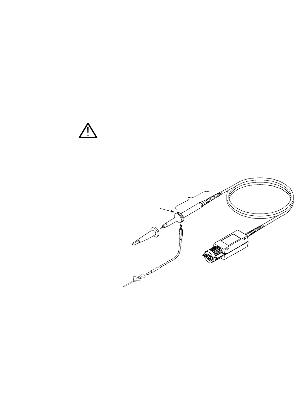
Grounding the Probe
Connect the probe to the instrument and connect the ground lead to
ground before making any measurements. Ensure that no part of the
ground lead contacts voltage in the circuit under test. Except for the
probe tip and BNC center conductor, all accessible metal (including
the ground clip) is connected to the BNC shell.
WARNING. To avoid electric shock when using the probe, keep your
fingers behind the finger guard on the probe body. See Figure 1–2
below.
Getting Started
Hand contact area
Finger
guard
Figure 1–2: Probe finger guard and hand contact area
P6205 Instruction Manual
1–7
Page 24

Getting Started
1–8
P6205 Instruction Manual
Page 25

Operating Basics
Page 26

Page 27
Operating Basics
This section discusses technical issues you should consider when
using the P6205 probe.
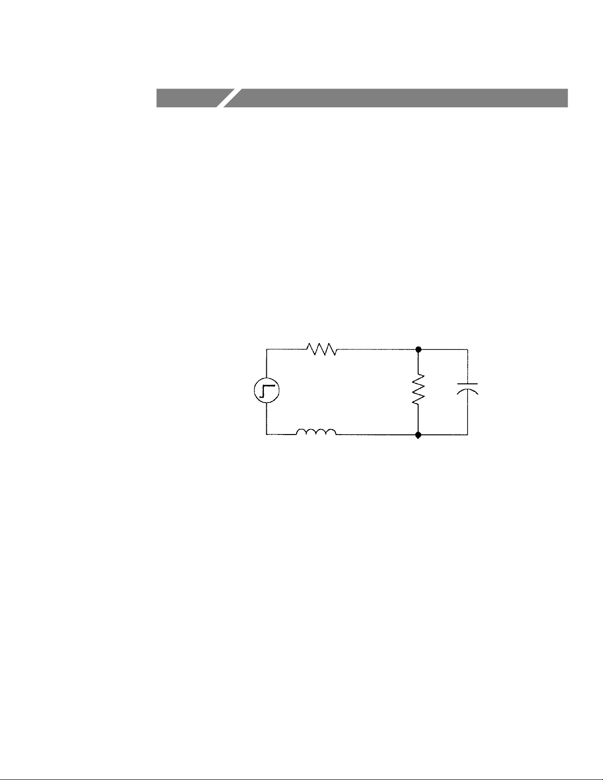
Ground Lead Inductance
When you touch the probe tip to a circuit element you are introducing a new resistance, capacitance, and inductance into the circuit.
See Figure 2–1.
R
source
V
Source
L
Ground lead
gl
Probe
Rin 1 M
Probe
C
= 2 pF
in
Figure 2–1: Equivalent circuit showing added probe and ground lead
resistance, capacitance, and inductance
The high input resistance of the P6205 probe has negligible effect on
most circuits. The series inductance introduced by the probe tip and
ground lead however, can result in a parasitic resonant circuit that
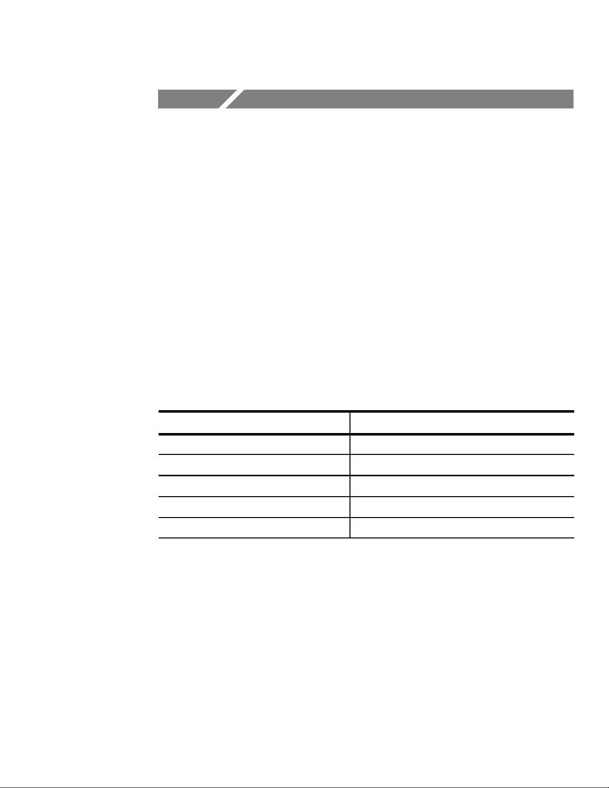
“rings” within the bandwidth of your oscilloscope system. Figure 2–2 shows examples of how different ground leads affect a
displayed signal.
P6205 Instruction Manual
2–1
Page 28

Operating Basics
50 mV/div
Low inductance ground
273 ps
6 inch ground lead
561 ps
2 ns/div
Figure 2–2: Effects of ground lead inductance on waveform fidelity
NOTE. Ringing and rise time degradation can be masked if the
frequency content of the signal degradation is beyond the bandwidth
of your oscilloscope system.
If you know the self-inductance (L) and capacitance (C) of your
probe and ground lead, use the following equation to determine the
approximate resonant frequency (f
f
0
1
2 LC
) of a parasitic circuit:
0
From this equation, you can see that the desired goal is to lower the
probe and ground lead inductance until the frequency of any
parasitic oscillation is well beyond the desired frequency of the
measurement. The low-inductance ground contact can help reduce
the effects of ground lead inductance.
2–2
P6205 Instruction Manual
Page 29

Linear Operating Range
The internal probe amplifier has a finite operating range when
terminated into a 50 W load. To maintain a linearity error below 4%,
limit the input signal amplitude to ±10 V. Refer to Figure 3–3 on
page 3–6 for data on linear operating range.
NOTE. The P6205 probe can sustain input voltages to ±40 V without
damage; however, the linearity err or specification does not apply to
input voltages exceeding ±10 V.
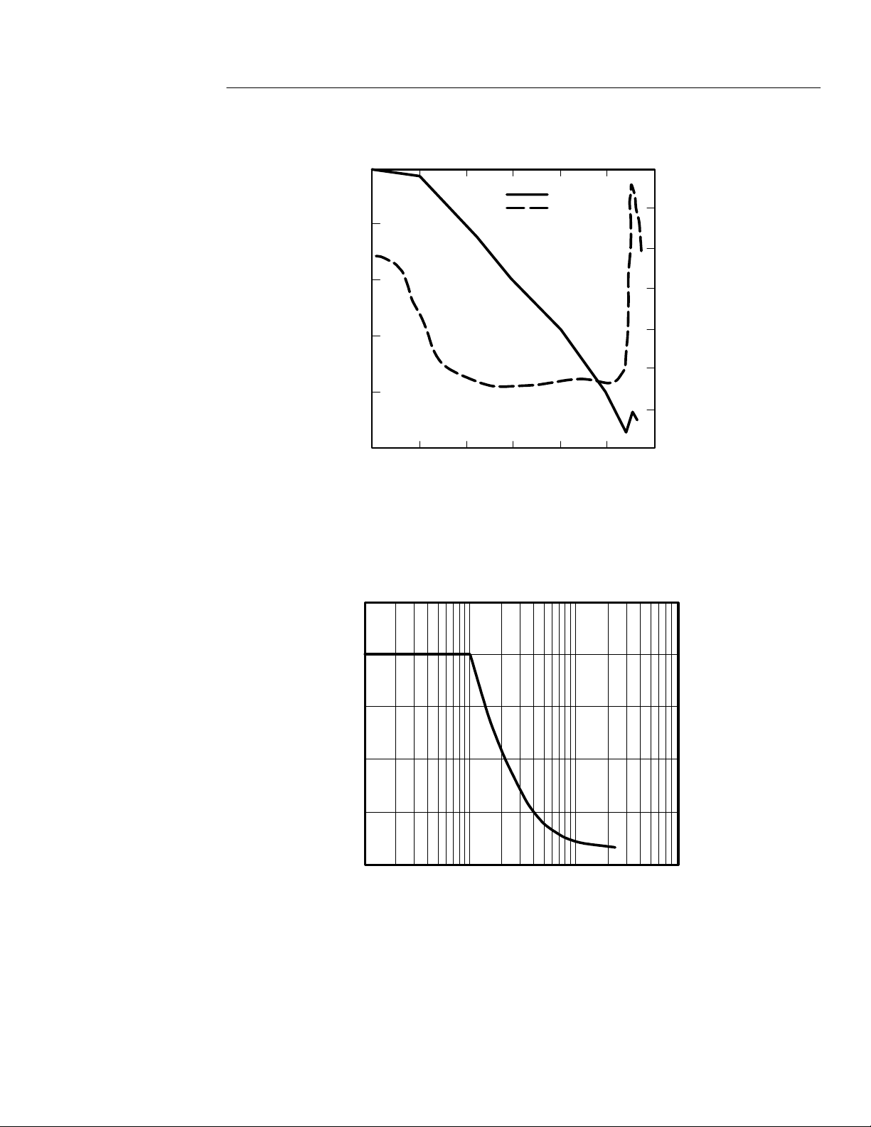
High-Amplitude Frequency Response
Operating Basics
Input signal amplitude also affects probe frequency response. Figures
2–3 and 2–4 characterize the effects of probe frequency response in
terms of rise time for step inputs and –3 dB bandwidth for sine wave
inputs.
Step Inputs
Degradation of high-amplitude step inputs generally appear as
slower rise times and distorted responses. Figure 2–3 shows probe
linear operating range as a function of input step voltage, in terms of
rise time and fall time.
P6205 Instruction Manual
2–3
Page 30

Operating Basics
2
1.5
1
Accurate measuring area
.5
Input signal rise time (ns)
0 2.5 V 5 V 7.5 V 10 V
2
1.5
Accurate measuring area
1
Input signal fall time (ns)
.5
Input step (V
Nonlinear area
step)
p–p
Nonlinear area
2–4
0 2.5 V 5 V 7.5 V 10 V
Input step (V
p–p
step)
Figure 2–3: P6205 typical input vs linear operating range
P6205 Instruction Manual
Page 31

Operating Basics
Sine Wave Inputs
Degradation of high-amplitude sine wave inputs generally appear as
harmonic distortion and reduced peak-to-peak amplitude. Figure 2–4
shows the –3 dB bandwidth of sine wave inputs as a function of
amplitude.
800
600
400
–3 dB frequency (MHz)
200
0246810
Amplitude (V
sinewave)
p–p
Figure 2–4: Bandwidth vs sine wave input amplitude
P6205 Instruction Manual
2–5
Page 32

Operating Basics
2–6
P6205 Instruction Manual
Page 33

Specifications
Page 34

Page 35
Specifications
This section lists the electrical, environmental, and physical
specifications of the P6205 probe. All specifications are guaranteed
unless labeled “typical”. Typical specifications are provided for your
convenience and are not guaranteed. Specifications marked with the
n symbol are verified in in the Performance Verification section
beginning on page 4–1.
The electrical characteristics listed in Table 3–1 apply to a probe
calibrated between 20_ C and 30_ C. The instrument system must
also be calibrated and operating within the environmental conditions
listed in Table 3–2 on page 3–4.
Following the specification tables you will find a series of graphs
showing typical probe characteristics.
T able 3–1: Electrical characteristics
Characteristic Description
nAttenuation
Input resistance
Input capacitance ≤2 pF
nRise time
Bandwidth
1
2,3
3
3
10X ±1.8% at DC into 50 ±0.5% load
1 M ±5% at DC
< 467 ps
Derived from rise time (BW = 0.35/tr): 750 MHz
P6205 Instruction Manual
3–1
Page 36

Specifications
T able 3–1: Electrical characteristics (Cont.)
Characteristic Description
Bandwidth, typical
Mainframe:
TDS500/600
TDS400
11402A/11403A
450 MHz
325 MHz
See plug-in unit
Plug-in unit:
11A32
11A33
11A34V
11A52
11A72
nAberrations
3,4
350 MHz
125 MHz
275 MHz
475 MHz
600 MHz
first 20 ns ±7%, 10% peak to peak
20 ns to 2 ms
±3%, 5% peak to peak
Propagation delay Probe tip to output connector measured at
waveform 50% points: 6.72 ns ±200 ps
nOutput offset
3,5
At 25_ C (77_ F): less than ±10 mV
±100 mV on screen for oscilloscopes that
recognize probe coding
Linearity
6
Linear input range ±10 V
Linearity error Relative to full-scale output with ±10 V input:
< 4%
DC Thermal drift
3,7
Less than ±100 mV/_C
For scopes that recognize probe coding: ±1 mV
on screen
Output load requirement
50 W ±0.5%
Maximum nondestructive input voltage 40 VDC + peak AC
3–2
P6205 Instruction Manual
Page 37

Specifications
T able 3–1: Electrical characteristics (Cont.)
Characteristic Description
Electrostatic immunity Sustains discharge from a 500 pF capacitor
charged to 10 kV, through a 1 k resistance to
connector pin.
Power supply requirements
the probe tip or a TEKPROBE
8
+5 V supply +5 V ±2%, 110 mA maximum
–5 V supply –5 V ±2%, 50 mA maximum
Power consumption Host instrument input power: 1.25 W maximum
1
11000 Series mainframes: use the probe calibrate function to gain additional
accuracy.
2
With probe operating.
3
Probe only.
4
When used with a system having a rise time of less than 100 ps, refer to
Aberrations in the Performance Verification section.
5
11000 Series oscilloscopes only: less than 2 mV following oscilloscope
calibration.
6
See page 2–4: Linear Operating Range.
7
At probe output.
8
Less accurate supply levels increase output offset error.
P6205 Instruction Manual
3–3
Page 38

Specifications
T able 3–2: Environmental characteristics
Characteristic Description
Temperature range
Operating
0_ C to +50_ C
(32_ F to 122_ F)
Nonoperating
–55_ C to +75_ C
(–67_ F to 167_ F)
Humidity Five cycles (120 hr) at 90 to 95% relative
humidity
Altitude
Operating To 4,600 m (15,000 ft)
Transportation Qualifies under National Safe Transit Associa-
tion Preshipment Procedure 1–A–B–1
T able 3–3: Physical characteristics
Characteristic Description
Shipping weight
1
0.9 kg (2 lbs)
Probe cable length 1.5 m (60 in) tip to BNC
1
Includes accessories.
T able 3–4: Certifications and compliances
Pollution degree Degree 2
Safety class Class 1 (ground reference)
3–4
P6205 Instruction Manual
Page 39
Specifications
1M
ohms
degrees
100k
10k
1k
Magnitude (ohms)
100
10
10kHz 100kHz 1MHz 10MHz 100MHz1GHz 10GHz
Frequency
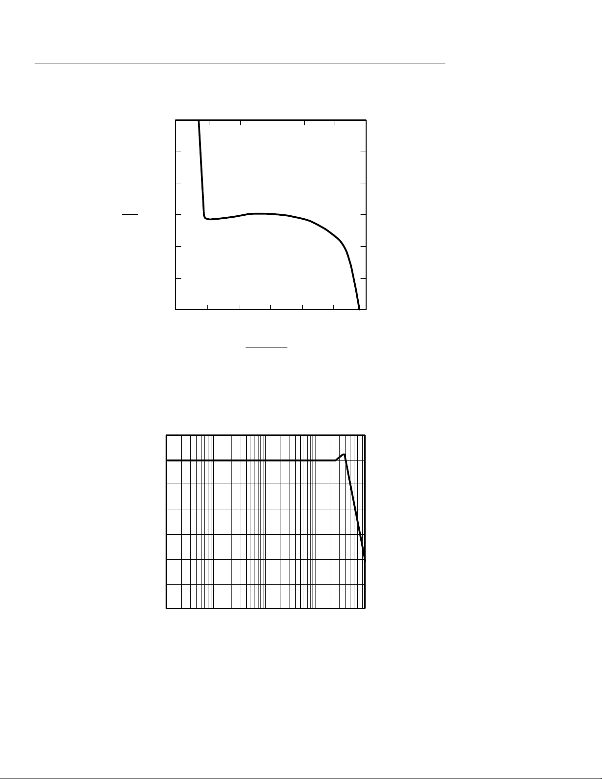
Figure 3–1: T ypical input impedance vs frequency
+50
+25
0
–25
–50
Phase (degrees)
–75
–100
–125
50
40
30
20
Maximum input voltage (V)
10
0
100MHz10MHz 1GHz 10GHz
Frequency
Figure 3–2: Voltage derating vs frequency
P6205 Instruction Manual
3–5
Page 40
Specifications
V
out
+15mV
+10mV
+5mV
V
in
–
0
10
–5mV
–10mV
–15mV
–15/10 –10/10 –5/10 0 +5/10 +10/10 +15/10
V
in
Attenuation
Figure 3–3: Linearity error vs output voltage
1
0
–1
–2
V
(dB)
out
–3
–4
–5
–6
100kHz 1MHz 10MHz 100MHz 1GHz
3–6
Frequency
Figure 3–4: Typical frequency response
P6205 Instruction Manual
Page 41

Performance Verification
Page 42

Page 43

Performance Verification
This section contains procedures to verify that the P6205 probe
meets the performance requirements listed in the Specifications
section. The performance verification procedures consists of the
following checks:
Attenuation
Rise Time
Aberrations
Output offset
Performance characteristics not verified by the performance
verification procedures are either extremely stable or impractical to
verify.
Use the performance verification procedures as an acceptance
criteria or to verify probe performance following repair.
Under normal operating conditions, verify the performance of your
probe at least once a year.
Test Equipment
Table 4–1 lists the recommended test equipment used in the
performance verification procedures. The equipment recommended
is the minimum necessary to provide accurate results. Substitute
equipment must meet or exceed the specifications listed.
If you are unfamiliar with the operation of the recommended test
equipment, refer to the individual users manuals for instructions.
NOTE. Before beginning any performance verification procedure,
warm up all test equipment for at least 20 minutes.
P6205 Instruction Manual
4–1
Page 44

Performance Verification
Table 4–1: Test equipment
Description Minimum Requirement Example Product
Oscilloscope
Probe power supply TEKPROBE interface con-
Calibration generator Amplitude accuracy: ±0.25% Calibration signal from
Pulse generator Rise time: <100 ps Calibration signal from
Termination adapter
Female BNC-to-GR adapter Tektronix part number
Male SMA-to-BNC female
adapters (2)
Male SMA-to-GR adapter Tektronix part number
Coaxial cable
DC to 10 GHz, 50 W input
nector
50 W, probe-to-GR
50 W BNC, 10 inch length
Tektronix 11801B with
SD-24 TDR sampling head
Tektronix 1103 TEKPROBE
power supply
11801B oscilloscope
11801B oscilloscope
Tektronix part number
017-0088-00
017-0063-00
Tektronix part number
015-0554-00
015-1007-00
Tektronix part number
012-0208-00
Attenuation Check
Use the following procedure to confirm that the P6205 probe
performs within its Attenuation specification limits.
1. Set the oscilloscope controls as indicated in the table below.
Oscilloscope settings
Control Setting
Volts/division 50 mV
Time/division
4–2
2 ms
P6205 Instruction Manual
Page 45

Performance Verification
Oscilloscope settings (Cont.)
Control Setting
Trigger source Internal clock
Trigger mode Auto
Coupling DC
Waveform averaging On
Number of waveforms to average 8
Cursor type Horizontal bars
Cursor knob resolution Fine
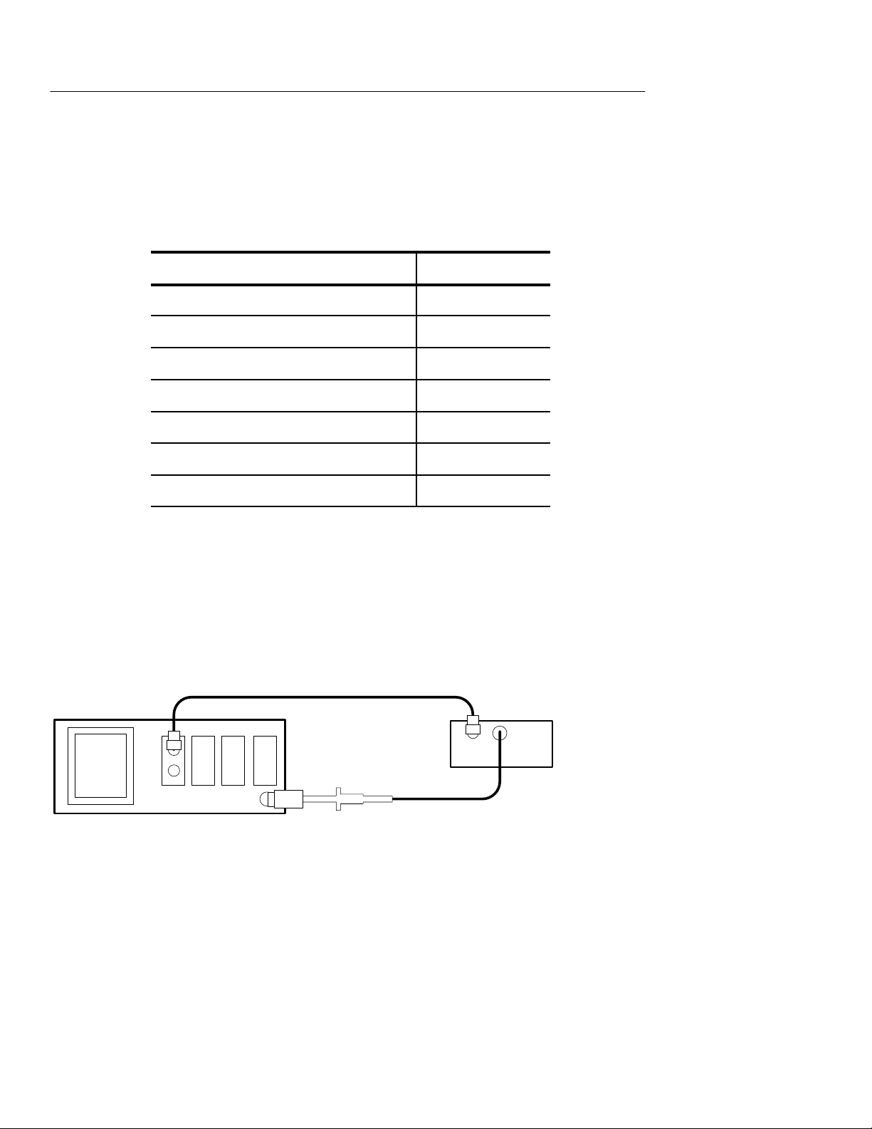
2. Install one SMA-to-BNC adapter on an SD-24 sampling head
input channel and another adapter on the oscilloscope calibrator
output. Use the 10-inch coaxial cable to connect the oscilloscope
calibrator output to the SD-24 input channel. See Figure 4–1
below.
11801B oscilloscope
Figure 4–1: Attenuation test setup part 1
3. Press SELECT CHANNEL on the sampling head to enable the
corresponding input channel.
4. Adjust the oscilloscope controls as necessary to display a
waveform similar to the one shown in Figure 4–2 below.
P6205 Instruction Manual
4–3
Page 46

Performance Verification
Figure 4–2: Calibrator waveform
5. Store and then recall the waveform.
6. Use the oscilloscope cursors to display the D voltage of the
recalled waveform. Measure the low-frequency portion of the
waveform near the back corner. See figure 4–3 below.
4–4
Figure 4–3: Cursors placement for voltage measurement
7. Record the D voltage as V
.
1
8. Disconnect the coaxial cable from the oscilloscope calibrator
output and reconnect it to the channel 1 output of the 1103 probe
power supply. Remove the SMA-to-BNC adapter from the
oscilloscope calibrator output.
9. Connect the P6205 probe output to the 1103 power supply
channel 1 input. The P6205 does not use the offset capability of
the 1103 power supply; the offset control setting is not important.
10.Mate the GR connector ends of the 50 W termination adapter and
the male SMA-to-GR adapter . Connect the mated assembly to the
oscilloscope calibrator output. Insert the probe tip firmly into the
50 W termination adapter . See Figure 4–4 below.
P6205 Instruction Manual
Page 47

11801B
oscilloscope
Figure 4–4: Attenuation test setup part 2
11. Adjust the oscilloscope vertical position control if necessary to
center the resulting waveform. Store and then recall the
waveform.
12.Use the cursor measurement capability of the oscilloscope to
display the D voltage of the recalled waveform. Measure the
low-frequency portion of the waveform near the back corner.
Record the D voltage as V
Performance Verification
1103 power supply
.
2
13.Use the following equation to calculate the attenuation error:
%error +
14.Verify that the probe attenuation error is ≤1.8%.
Rise Time Check
Use the following procedure to confirm that the P6205 probe
performs within its Rise Time specification limits.
NOTE. If you do not have access to an 11800 Series oscilloscope, a
method for approximating probe rise time using a pulse generator
and a TDS 500 or 11000 Series oscilloscope follows this procedure.
V
(10) –V
2
V
1
1
100
P6205 Instruction Manual
4–5
Page 48
Performance Verification
1. Set the oscilloscope controls as indicated in the table below.
Oscilloscope settings
Control Setting
Volts/division 5 mV
Time/division 500 ps
Trigger coupling DC
Trigger source Internal clock
Trigger mode Auto
Waveform averaging On
Number of waveforms to average 8
2. Connect one end of the 10-inch coaxial cable to the channel 1
output of the 1103 probe power supply. Use a male SMA-to-BNC
female adapter to connect the free end of the cable to an SD-24
sampling head input. See Figure 4–5 below.
11801B
oscilloscope
Figure 4–5: Rise time test setup
3. Press SELECT CHANNEL on the sampling head to enable the
corresponding input channel.
1103 power supply
4–6
4. Connect the P6205 probe to the 1103 probe power supply
channel 1 input. The P6205 does not use the offset capability of
P6205 Instruction Manual
Page 49

Performance Verification
the 1103 probe power supply; the offset control setting is not
important.
5. Mate the GR ends of the male SMA-to-GR and 50 W termination
adapters. Connect the mated assembly to the oscilloscope
calibrator output. Insert the P6205 probe tip firmly into the
termination adapter. See Figure 4–5 above.
6. Adjust the oscilloscope horizontal and vertical position controls
to display a waveform similar to the one shown in Figure 4–6
below.
Figure 4–6: Rise time waveform
7. Use the oscilloscope measurement capability to display and
measure the waveform rise time (from the 10% to 90% amplitude
points).
8. Verify that the probe rise time is equal to or less than 467 ps.
Rise Time Approximation
Use the following procedure to approximate the probe rise time
without an 11801B oscilloscope. The procedure requires a pulse
generator capable of producing a rise time step of 250 ps or less.
1. Use a 50 W coaxial cable to connect the output of the pulse
generator directly to the oscilloscope input.
2. Set the time base to 1 ns/division and the vertical amplifier to
50 mV/division. Adjust the pulse for a duration of greater than
10 ns with an amplitude of 250 mV.
3. Save and then recall the waveform.
P6205 Instruction Manual
4–7
Page 50

Performance Verification
4. Measure and record as system rise time (tr
), the rise time of the
s
displayed pulse.
5. Mate the 50 W termination adapter to the female BNC-to-GR
adapter. Disconnect the coaxial cable at the oscilloscope and
attach the mated adapters to the coaxial cable. Connect the P6205
probe to the same oscilloscope input and insert the probe tip
firmly into the termination adapter.
6. Save and then recall the waveform.
7. Adjust the oscilloscope controls to display this waveform at the
same vertical scale as the first waveform. Measure and record as
probe-plus-system rise time (tr
), the rise time of the displayed
p+s
pulse.
8. Calculate the probe rise time (tr
) using the equation below.
p
Accuracy of the approximation is limited by oscilloscope system
performance.
t
r
+ t
p
Ǹ
r
p)s
2
–t
r
2
s
The calculated probe rise time should be less than 467 ps. If the rise
time value exceeds this limit, use the procedure beginning on
page 4–5 to more accurately determine the probe rise time.
Bandwidth Approximation
You can calculate the approximate bandwidth from the rise time
measurement with the following equation:
BW +
.35
t
r
NOTE. This calculation does not constitute a valid performance
verification criteria.
4–8
P6205 Instruction Manual
Page 51

Aberrations Check
Use the following procedure to confirm that the P6205 probe
performs within its Aberrations specifications limits.
1. Set the oscilloscope controls as indicated in the table below.
Oscilloscope settings
Control Setting
Volts/division 50 mV
Time/division 500 ps
Trigger coupling DC
Trigger source Internal clock
Performance Verification
Trigger mode Auto
Waveform averaging On
Number of waveforms to average 8
2. Install one SMA-to-BNC adapter on an SD-24 sampling head
input channel and another adapter on the oscilloscope calibrator
output. Use the 10-inch coaxial cable to connect the oscilloscope
calibrator output to the SD-24 input channel. See Figure 4–7
below.
11801B oscilloscope
Figure 4–7: Aberrations test setup part 1
P6205 Instruction Manual
4–9
Page 52

Performance Verification
3. Press SELECT CHANNEL on the sampling head to enable the
corresponding input channel.
4. Adjust the oscilloscope controls as necessary to display a
waveform similar to the one shown in Figure 4–8 below.
Figure 4–8: Aberrations waveform
5. Use the oscilloscope rise time filter capability to limit the
waveform rise time to 100 ps. Use the waveform Vertical
Description menu to set the vertical description as follows:
Filter(M1,100E-12)
NOTE. The filter description above applies to an SD-24 sampling
head installed in the 11801B mainframe M1 plug-in compartment; if
your sampling head is installed in a different compartment, select the
corresponding mainframe designator.
6. Use the oscilloscope measurement capability to determine the
peak-to-peak amplitude of the filtered pulse. Measure, calculate,
and record (in percent) the system aberrations (abs
) in the first
s
4 ns of the waveform.
NOTE. Part one of the aberrations specification applies to the first
20 ns of the waveform. Significant aberrations are usually completely damped beyond approximately 4 ns.
4–10
P6205 Instruction Manual
Page 53

Measure the peak negative-going aberration (if any) and the peak
positive-going aberration (if any). The sum of the two is the
peak-to-peak aberration, in percent.
NOTE. If the waveform front corner appears rounded or rolled-off, set
the left-limit measurement cursor at the first 100% amplitude point
of the waveform to determine aberrations. Refer to Figure 4–9.
Positive aberration
Performance Verification
Peak-to-peak aberration
Negative aberration
100%
90%
10%
Figure 4–9: Measuring aberrations
7. Disconnect the coaxial cable from the oscilloscope calibrator
output and reconnect it to the channel 1 output of the 1103 probe
power supply. Remove the SMA-to-BNC adapter from the
oscilloscope calibrator output. See Figure 4–10 below.
20ns
2ms
Rise time
8. Connect the P6205 probe output to the 1103 power supply
channel 1 input. The P6205 does not use the offset capability of
the 1103 probe power supply; the offset control setting is not
important.
P6205 Instruction Manual
4–1 1
Page 54

Performance Verification
9. Mate the GR connector ends of the 50 W termination adapter and
the male SMA-to-GR adapter . Connect the mated assembly to the
oscilloscope calibrator output. Insert the probe tip firmly into the
50 W termination adapter .
11801B
oscilloscope
Figure 4–10: Aberrations test setup part 2
1103 power supply
10.Press SELECT CHANNEL on the sampling head to enable the
corresponding input channel.
11. Set the oscilloscope volts/division to 5 mV.
12.Adjust the oscilloscope horizontal and vertical position controls
to display a waveform similar to the one shown in Figure 4–8
above.
13.Ensure that Waveform Averaging is enabled. Ensure that the
vertical description rise time filter is enabled. If not, repeat
Step 5 above.
14.Use the oscilloscope measurement capability to determine the
peak-to-peak amplitude of the pulse. Measure, calculate, and
record (in percent) the probe-plus-system aberrations (abs
p+s
) in
the first 4 ns of the waveform. Measure the peak negative-going
aberration (if any) and the peak positive-going aberration (if
any). The sum of the two is the peak-to-peak aberration in
percent.
4–12
P6205 Instruction Manual
Page 55

Performance Verification
NOTE. If the waveform front corner appears rounded or rolled-off, set
the left-limit measurement cursor at the first 100% amplitude point
of the waveform. Refer to Figure 4–9 above.
15.The probe aberrations are approximately the difference between
the measured probe aberrations and the oscilloscope system
aberrations. Subtract the system aberrations (Step 6) from the
measured aberrations (Step 14) for both the peak and the
peak-to-peak aberrations.
abs
+ abs
p
p)s
– abs
s
NOTE. In some cases the measured aberrations are less than the
system aberrations. This situation occurs when the slower rise time
of the probe (compared to the oscilloscope/sampling head combination) filters out a portion of the higher-frequency aberrations.
16.Verify that the probe-only aberrations meet specifications:
peak, first 20 ns ±7%
peak to peak, first 20 ns 10%
17.Repeat steps 1 through 15 above using an oscilloscope sweep
speed of 500 ns per division. Adjust the oscilloscope as necessary
to display one pulse step and at least 2 ms of settling time.
Optional: Increasing the number of waveforms averaged will
reduce the effects of noise on the smaller aberrations in the latter
part of the signal.
18.Verify that the probe-only aberrations meet specifications:
peak, 20 ns to 2 ms ±3%
peak to peak, 20 ns to 2 ms5%
P6205 Instruction Manual
4–13
Page 56
Performance Verification
Output Offset Check
Use the following procedure to confirm that the P6205 probe
performs within its Output Offset specification limits.
1. Set the oscilloscope controls as indicated in the table below.
Oscilloscope settings
Control Setting
Volts/division 2 mV
Trigger coupling DC
Time/division 1 ps
Trigger mode Auto
Enhanced accuracy On
2. Install an SMA-to-BNC adapter on one of the SD-24 sampling
head inputs. Use a 10-inch coaxial cable to connect the output of
the 1103 probe power supply to an SD-24 input channel.
3. Press SELECT CHANNEL on the sampling head to enable the
corresponding input channel.
4. Adjust the oscilloscope offset or position control to center the
trace at 0 V (or less than 1 mV).
Optional method: Use the oscilloscope measurement capability to
display the mean voltage of the free-running trace.
5. Insert the P6205 probe tip firmly into the 50 W termination
adapter. (The BNC end remains unused.)
6. Connect the probe output to the 1103 probe power supply input.
7. Verify that the probe output offset (displacement of the
free-running trace) is less than ±10 mV.
4–14
P6205 Instruction Manual
Page 57

Maintenance
Page 58

Page 59
Maintenance
The Maintenance section provides information on the following
topics:
Inspecting and cleaning the probe
Replacing the probe tip
Replacing TEKPROBE contact pins
Replacing internal modules
Packaging the probe for shipment
Preventive Maintenance
Preventive maintenance consists of visually inspecting and cleaning
the probe. Perform preventive maintenance on a regular basis to
prevent breakdown and improve reliability. The frequency of
maintenance depends on the environmental operating conditions. A
good time to perform maintenance is just before a performance
verification or calibration.
WARNING. To prevent electric shock, disconnect the probe from the
signal source and oscilloscope or power supply before performing
preventive maintenance.
Visual Inspection
The best indicator of probe condition is performance. In addition to
performing the performance verification procedures, occasionally
inspect the probe tip, body, cable, compensation box, and BNC
connector for bent, broken, or damaged parts. To ensure optimum
performance, replace damaged assemblies as soon as practical.
P6205 Instruction Manual
5–1
Page 60

Maintenance
Cleaning
Remove accumulated loose dust from the probe exterior with a soft
cloth or small brush. Remaining dirt may be removed with a soft
cloth dampened with a mild detergent and water solution. Do not
immerse the probe or use abrasive cleaners.
With normal use the interior of the probe compensation box does not
require cleaning. If you wish to clean the probe interior while
replacing internal assemblies, use dry low-velocity air (approximately 9 lbs/in
dirt with a soft cloth or small brush or a soft cloth dampened with a
nonresidue cleaner , such as isopropyl alcohol (IPA). Use a cottontipped swab to clean the circuit board or in narrow spaces.
CAUTION. To prevent damage to probe materials, avoid using
chemicals that contain benzene, toluene, xylene, acetone, or similar
solvents.
2
) to blow away accumulated dust. Remove any remaining
Corrective Maintenance
Corrective maintenance consists of replacing defective parts or
assemblies. To determine which parts are replaceable, refer to the
Replaceable Parts section beginning on page 6–1.
To guarantee probe performance, do not attempt to replace the
individual components of replaceable assemblies.
WARNING. To prevent electric shock, disconnect the probe from the
signal source and oscilloscope or power supply before performing
preventive maintenance.
5–2
P6205 Instruction Manual
Page 61

Maintenance
Static Sensitive Devices
The P6205 probe contains devices that are susceptible to damage
from static discharge. To prevent damage to static-sensitive devices,
observe the following precautions whenever the compensation box
covers are removed or you are handling component assemblies:
Minimize the handling of all components; handle components
only at a grounded static-free workstation.
Service component assemblies on metal or other conductive
surfaces. Do not slide assemblies across any surface.
Wear a grounding strap when handling component assemblies to
discharge static voltage from your body.
Avoid materials that are capable of generating a static charge.
Replacing the Probe Tip
To replace the probe tip, use a pair of needle-nosed pliers to
carefully unscrew the old tip and install the new tip. Use care to
avoid stripping the plastic threads in the tip insulator and to avoid
damaging the new tip during installation. Following removal, probe
tips should be discarded in the appropriate receptacle. Tektronix
recommends that you do not reuse probe tips.
Replacing the TEKPROBE Contact Pins
To replace a TEKPROBE interface contact pin, use a pair of
needle-nosed pliers to pull the pin straight out of the BNC assembly.
To install a new pin, hold the pin carefully with the needle-nosed
pliers while pushing it into the BNC assembly. Use care to avoid
crushing or bending the hollow pin. Verify that the installed pin is
seated to the same depth as the other pins.
P6205 Instruction Manual
5–3
Page 62

Maintenance
Replacing Internal Assemblies: Probe Head and Cable, BNC and Circuit
Board Carrier
The steps required to replace the probe head and cable or BNC and
circuit board carrier assemblies are identical.
Probe Disassembly. Refer to Figure 5–1 and use the following
procedure to disassemble the P6205 probe.
1. Use a small, flat screwdriver (or the optional compensation box
NOTE. To prevent destructive cable flex, hold the cable boot and
BNC connector secur ely in the bottom cover as you separate the
compensation box halves to remove the top cover.
release tool) to pry the compensation box cover slots off the tabs
that secure it to the compensation box base.
2. When all four tabs are released, carefully pry open and remove
the top cover.
3. Taking care to minimize cable flex, lift the cable boot and BNC
connector from the cradle of the bottom cover.
NOTE. For subsequent reassembly in the procedures to follow, note
the orientation of the BNC locking ring tab with respect to the
bottom cover (ther e is also a small notch in the circuit board carrier
with a corresponding tab in the compensation box slot).
4. Locate and desolder at the circuit board, the red and black wires
from the cable assembly. Locate and desolder at the circuit board,
the uninsulated ground wire emerging from the cable assembly.
Note the position of all wires for reassembly in the procedure to
follow.
5. Grasp the probe cable close to the BNC end and withdraw the
cable from its connector in the center of the circuit board. Take
care to pull the cable straight out.
5–4
P6205 Instruction Manual
Page 63
Maintenance
Figure 5–1: Disassembling the P6205 probe
Probe Resassembly. Refer to Figure 5–1 and use the following
procedure to reassemble the P6205 probe.
1. Verify that the center conductor of the probe cable is straight and
centered in its connector; the center conductor must align with a
receptacle seated deeply within the BNC and circuit board carrier
assembly.
2. Insert the probe cable into the receptacle in the center of the BNC
and circuit board carrier until it is fully seated. After inserting the
cable, handle the assembly carefully to minimize strain on the
BNC and cable assembly .
3. Taking care to minimize cable flex, insert the cable boot and
circuit board carrier into their respective slots in the compensation box bottom cover .
4. Resolder the red and black wires to their respective connections
on the circuit board. Resolder the uninsulated ground wire to its
connection on the circuit board.
5. Position the red and black wires so they will not be pinched when
you attach the compensation box top cover .
P6205 Instruction Manual
5–5
Page 64

Maintenance
6. Align the tabs of the top cover with the slots of the bottom cover
and circuit board carrier. Press the cover into place and verify
that the bottom cover tabs snapped into the top cover slots.
Readjustment Following Repair
Following probe repair or parts replacement, complete the
performance verification procedures to ensure the probe is operating
within specifications. The performance verification procedure begin
on page 4–1.
Repackaging for Shipment
If you must ship your probe for repair, use the original packaging
container if possible. If the container is unfit for use or not available,
repackage the probe as follows:
1. Use a carton with a test strength of no less than 175 pounds.
2. Surround the probe with protective polyethylene sheeting.
3. Cushion the probe on all sides with at least two inches of tightly
packed urethane foam or other packing material.
4. Seal the carton with shipping tape or an industrial stapler .
5–6
P6205 Instruction Manual
Page 65

Replaceable Parts
Page 66

Page 67

Replaceable Parts
This section contains a list of the replaceable modules for the P6205
probe. Use this list to identify and order replacement parts.
Parts Ordering Information
Replacement parts are available through your local Tektronix field
office or representative.
Changes to Tektronix products are sometimes made to accommodate
improved components as they become available and to give you the
benefit of the latest improvements. Therefore, when ordering parts, it
is important to include the following information in your order:
Part number
Instrument type or model number
Instrument serial number
Instrument modification number, if applicable
If you order a part that has been replaced with a different or
improved part, your local Tektronix field office or representative will
contact you concerning any change in part number .
Change information, if any, is located at the rear of this manual.
Module Servicing
Modules can be serviced by selecting one of the following three
options. Contact your local Tektronix service center or representative
for repair assistance.
Module Exchange. In some cases you may exchange your module for a
remanufactured module. These modules cost significantly less than
new modules and meet the same factory specifications. For more
information about the module exchange program, call 1-800-TEKWIDE, extension 6630.
P6205 Instruction Manual
6–1
Page 68

Replaceable Parts
Module Repair and Return. You may ship your module to us for repair,
after which we will return it to you.
New Modules. You may purchase replacement modules in the same
way as other replacement parts.
Using the Replaceable Parts List
This section contains a list of the mechanical and or electrical
components that are replaceable for the P6205 probe. Use this list to
identify and order replacement parts. The following table describes
each column in the parts list.
Parts list column descriptions
Column Column name Description
1 Figure & index number Items in this section are referenced by figure and
index numbers to the exploded view illustrations
that follow.
2 Tektronix part number Use this part number when ordering replacement
parts from Tektronix.
3 and 4 Serial number Column three indicates the serial number at
which the part was first effective. Column four
indicates the serial number at which the part was
discontinued. No entry indicates the part is good
for all serial numbers.
5 Qty This indicates the quantity of parts used.
6 Name & description An item name is separated from the description
by a colon (:). Because of space limitations, an
item name may sometimes appear as incom-
plete. Use the U.S. Federal Catalog handbook
H6-1 for further item name identification.
7 Mfr. code This indicates the code of the actual manufactur-
er of the part.
8 Mfr. part number This indicates the actual manufacturer ’s or
vendor’s part number.
6–2
P6205 Instruction Manual
Page 69

Replaceable Parts
Abbreviations
Abbreviations conform to American National Standard ANSI
Y1.1–1972.
Mfr. Code to Manufacturer Cross Index
The table titled Manufacturers Cross Index shows codes, names, and
addresses of manufacturers or vendors of components listed in the
parts list.
Manufacturers cross index
Mfr.
code
18359 PYLON CO. INC. 51 NEWCOMB ST ATTLEBORO, MA
Manufacturer Address City, state, zip code
02703–1403
24931 BERG ELECTRONICS INC BERG ELECTRONICS
RF/COAXIAL DIV
2100 EARLYWOOD DR
PO BOX 547
80009 TEKTRONIX INC 14150 SW KARL BRAUN DR
PO BOX 500
8X345 NORTHWEST SPRING MFGCO5858 WILLOW LANE LAKE OSWEGO, OR 97035
TK2548 XEROX CORPORATION 14181 SW MILLIKAN WAY BEAVERTON, OR 97005
TK2565 VISION PLASTICS INC 26000 SW PARKW AY
CENTER DRIVE
FRANKLIN, IN 46131
BEAVERTON, OR
97077–0001
WILSONVILLE, OR 97070
P6205 Instruction Manual
6–3
Page 70
6–4
Replaceable Parts
3
2
1
5
P6205 Instruction Manual
6
Figure 6–1: P6205 probe with standard accessories
8
7
4
9
10
11
12
Page 71

Replaceable parts: P6205 probe and standard accessories
Fig. &
index
number
Tektronix
part number
Serial no.
effective
Serial no.
discont’d
Qty Name & description Mfr. code Mfr. part number
6–1 –1 013–0107–06 1 TIP ,PROBE:MINIATURE/COMP ACT
SIZE,RETRACT ABLE HOOK ASSY
–2 131–4280–00 1 CONTACT,ELEC:PROBE TIP 80009 131–4280–00
–3 206–0438–00 1 PROBE HEAD ASSY:W/CABLE ASSY,1.5M,P6205 80009 206–0438–00
–4 200–3760–00 1 COVER,COMP BOX:TOP AND BOTTOM,W/LABEL &
RELEASE TOOL
–5 131–5352–00 1 CONNECTOR ASSY:W/CKT BD ASSY,4 PINS &
COVER
–6 131–3627–01 1 CONTACT,ELEC:GOLD PLATED TIP 18359 P–6158–1
STANDARD ACCESSORIES
020–1629–01 1 ACCESSORY KIT:P6203/P6204/P6205/P6206 80009 020–1629–00
–7 196–3120–00 1 LEAD,ELECTRICAL:23 AWG,6.0 L,GROUND 80009 196–3120–00
–8 206–0364–00 1 TIP,PROBE:MICROCKT TEST,0.05 CTR 80009 206–0364–00
–9 166–0404–01 1 COVER,GROUND 80009 66–0404–01
–10 196–3198–00 1 LEAD,ELECTRICAL:26 AWG,6.0 L 80009 196–3198–00
–11 214–4125–00 1 CONTACT,ELEC:TIP,GROUND 80009 214–4125–00
–12 – – – – – – – 1 TIP,PROBE:IC TEST
(SEE FIGURE 6–2)
80009 013–0107–06
80009 200–3760–00
80009 131–5352–00
Replaceable Parts
6–5P6205 Instruction Manual
070–8202–01 1 MANUAL,TECH:P6205 80009 070–8202–01
Page 72
Replaceable Parts
6–6
Figure 6–2: P6205 probe optional accessories
P6205 Instruction Manual
Page 73

Replaceable parts: P6205 probe optional accessories
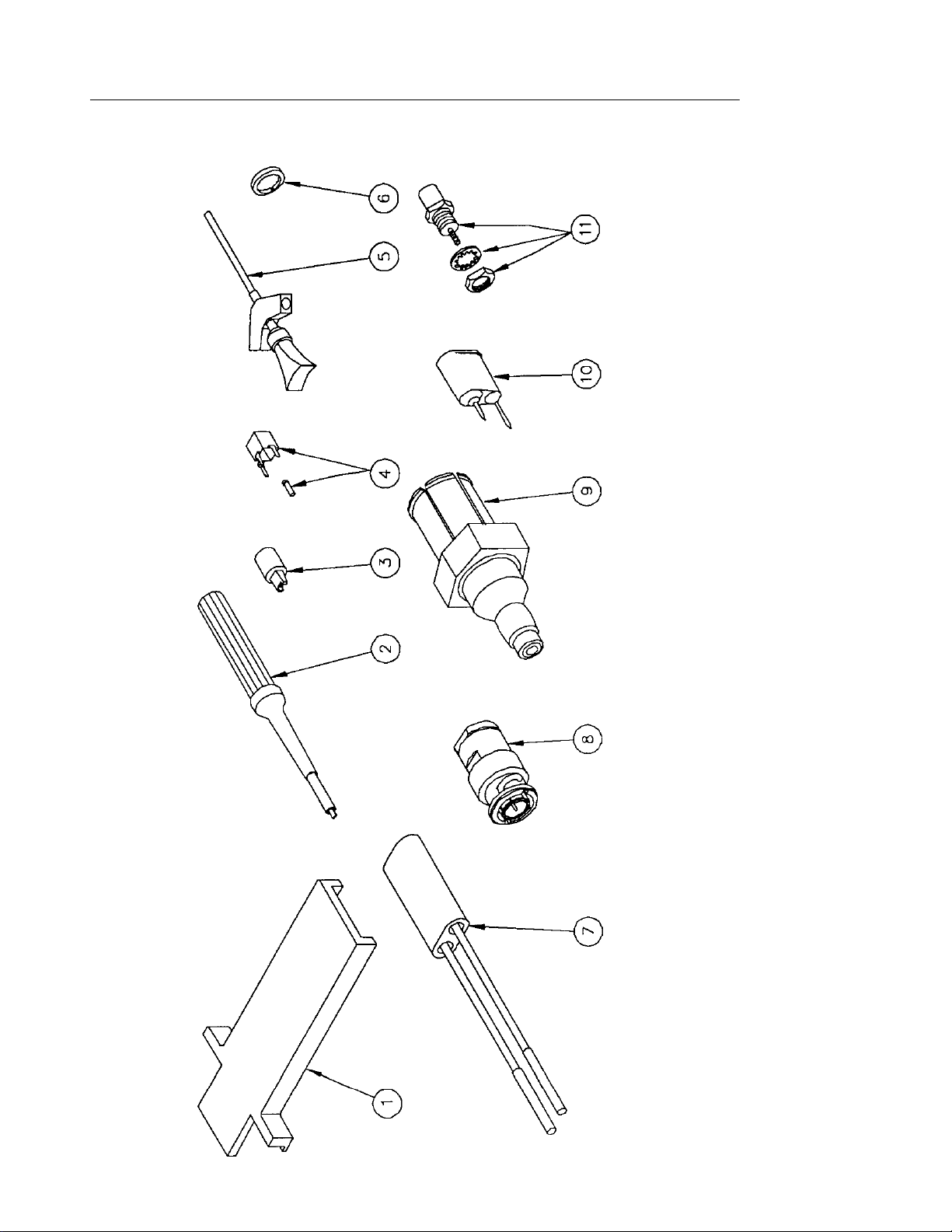
Fig. &
index
number
6–2 –1 003–1383–00 1 RLSE TOOL,COVER:COMP BOX,POLYCARBONATE TK2565 003–1383–00
–2 003–1433–00 1 SCREWDRIVER:ADJUSTMENT TOOL,METAL TIP TK2565 003–1433–00
–3 015–0201–07 1 TIP,PROBE:IC TEST,PKG OF 10 80009 015–0201–07
–4 031–4353–00 1 CONNECTOR,PROBE:PACK OF 25 80009 031–4353–00
–5 – – – – – – – 1 SMG50,SMT KLIPCHIP:20 ADAPTERS
Tektronix
part number
003–1433–01 1 SCREWDRIVER:ADJUSTMENT TOOL,PKG OF 5 80009 003–1433–01
015–0201–08 1 TIP,PROBE:IC TEST,PKG OF 100 80009 015–0201–08
Serial no.
effective
Serial no.
discont’d
Qty Name & description Mfr. code Mfr. part number
OPTIONAL ACCESSORIES
200–3760–00 1 COVER,COMP BOX:TOP AND BOTTOM,W/LABEL &
–6 016–0633–00 1 MARKER SET,CA:2 EA VARIOUS COLORS 80009 016–0633–00
–7 015–0325–00 1 ADAPTER,PROBE:PROBE TO CONNECTOR PINS TK2565 015–0325–00
–8 013–0084–01 1 ADAPTER,CONN:BNC TO PROBE 24931 28P156–1
–9 017–0088–00 1 CONN,PLUG,ELEC:50 OHM,GR 80009 017–0088–00
–10 013–0085–00 1 TIP,PROBE:GROUNDING 80009 013–0085–00
–11 131–0258–00 1 CONN,RCPT,ELEC:MINIATURE TIP SIZE,TEST JACK 24931 33JR115–2
6–7P6205 Instruction Manual
80009 200–3760–00
RELEASE TOOL
Replaceable Parts
Page 74

Replaceable Parts
6–8
P6205 Instruction Manual
 Loading...