

Page 1

Instruction Manual
P6135A
Differential Probe Pair
070-7675-02
Warning
The servicing instructions are for use by qualified
personnel only. To avoid personal injury, do not
perform any servicing unless you are qualified to
do so. Refer to all safety summaries prior to
performing service.
www.tektronix.com
Page 2

Copyright © Tektronix, Inc. All rights reserved.
T ektronix products are covered by U.S. and foreign patents, issued and
pending. Information in this publication supercedes that in all previously
published material. Specifications and price change privileges reserved.
T ektronix, Inc., P.O. Box 500, Beaverton, OR 97077
TEKTRONIX and TEK are registered trademarks of T ektronix, Inc.
KLIPCHIP is a trademark of T ektronix, Inc.
Page 3

WARRANTY
Tektronix warrants that the products that it manufactures and sells will be free from defects
in materials and workmanship for a period of one (1) year from the date of purchase from
an authorized Tektronix distributor. If any such product proves defective during this
warranty period, Tektronix, at its option, either will repair the defective product without
charge for parts and labor, or will provide a replacement in exchange for the defective
product. Batteries are excluded from this warranty.
In order to obtain service under this warranty, Customer must notify Tektronix of the defect
before the expiration of the warranty period and make suitable arrangements for the
performance of service. Customer shall be responsible for packaging and shipping the
defective product to the service center designated by Tektronix, shipping charges prepaid,
and with a copy of customer proof of purchase. Tektronix shall pay for the return of the
product to Customer if the shipment is to a location within the country in which the
Tektronix service center is located. Customer shall be responsible for paying all shipping
charges, duties, taxes, and any other charges for products returned to any other locations.
This warranty shall not apply to any defect, failure or damage caused by improper use or
improper or inadequate maintenance and care. Tektronix shall not be obligated to furnish
service under this warranty a) to repair damage resulting from attempts by personnel other
than Tektronix representatives to install, repair or service the product; b) to repair damage
resulting from improper use or connection to incompatible equipment; c) to repair any
damage or malfunction caused by the use of non-Tektronix supplies; or d) to service a
product that has been modified or integrated with other products when the effect of such
modification or integration increases the time or difficulty of servicing the product.
THIS WARRANTY IS GIVEN BY TEKTRONIX WITH RESPECT TO THE
LISTED PRODUCTS IN LIEU OF ANY OTHER WARRANTIES, EXPRESS OR
IMPLIED. TEKTRONIX AND ITS VENDORS DISCLAIM ANY IMPLIED
WARRANTIES OF MERCHANTABILITY OR FITNESS FOR A PARTICULAR
PURPOSE. TEKTRONIX’ RESPONSIBILITY TO REPAIR OR REPLACE
DEFECTIVE PRODUCTS IS THE SOLE AND EXCLUSIVE REMEDY
PROVIDED TO THE CUSTOMER FOR BREACH OF THIS WARRANTY.
TEKTRONIX AND ITS VENDORS WILL NOT BE LIABLE FOR ANY
INDIRECT, SPECIAL, INCIDENTAL, OR CONSEQUENTIAL DAMAGES
IRRESPECTIVE OF WHETHER TEKTRONIX OR THE VENDOR HAS
ADVANCE NOTICE OF THE POSSIBILITY OF SUCH DAMAGES.
Page 4

Page 5

Table of Contents
General Safety Summary v. . . . . . . . . . . . . . . . . . . . . . . . . . . .
Preface vii. . . . . . . . . . . . . . . . . . . . . . . . . . . . . . . . . . . . . . . . . . . .
Contacting T ektronix viii. . . . . . . . . . . . . . . . . . . . . . . . . . . . . . . . .
Getting Started
Product Description 1–1. . . . . . . . . . . . . . . . . . . . . . . . . . . . . . . . . .
Standard Accessories 1–2. . . . . . . . . . . . . . . . . . . . . . . . . . . . . . . . .
Probe Features 1–3. . . . . . . . . . . . . . . . . . . . . . . . . . . . . . . . . . . . . .
Grounding the Probe 1–5. . . . . . . . . . . . . . . . . . . . . . . . . . . . . . . . .
Choosing the Correct Probe Tip 1–6. . . . . . . . . . . . . . . . . . . . . . . .
Operating Basics
Probe Calibration 2–1. . . . . . . . . . . . . . . . . . . . . . . . . . . . . . . . . . . .
CMRR Considerations 2–1. . . . . . . . . . . . . . . . . . . . . . . . . . . . . . . .
Balancing Probe Pair Impedance Differences 2–2. . . . . . . . . . . . . .
Dynamic Range Effects 2–2. . . . . . . . . . . . . . . . . . . . . . . . . . . . . . .
Probe Grounding 2–3. . . . . . . . . . . . . . . . . . . . . . . . . . . . . . . . . . . .
Specifications
Performance V erification and
Calibration Procedures
T est Equipment 4–1. . . . . . . . . . . . . . . . . . . . . . . . . . . . . . . . . . . . .
Single-ended Applications 4–3. . . . . . . . . . . . . . . . . . . . . . . . . . . . .
Check and Adjust DC Attenuation 4–3. . . . . . . . . . . . . . . . . . .
Check and adjust low-frequency (LF) compensation 4–6. . . . .
Check and adjust high-frequency (HF) compensation 4–8. . . . .
Check bandwidth and system rise time 4–9. . . . . . . . . . . . . . . .
Common Mode Applications 4–12. . . . . . . . . . . . . . . . . . . . . . . . . . .
Check and Adjust DC Attenuation 4–12. . . . . . . . . . . . . . . . . . .
Check and Adjust LF and HF Compensation 4–14. . . . . . . . . . .
System Calibration and Time Delay Error Compensation
(11A33 only) 4–18. . . . . . . . . . . . . . . . . . . . . . . . . . . . . . . . .
P6135A Instruction Manual
i
Page 6

T able of Contents
Maintenance
Preventive Maintenance 5–1. . . . . . . . . . . . . . . . . . . . . . . . . . . . . . .
Visual Inspection 5–1. . . . . . . . . . . . . . . . . . . . . . . . . . . . . . . . .
Cleaning 5–1. . . . . . . . . . . . . . . . . . . . . . . . . . . . . . . . . . . . . . . .
Probe Tip Replacement 5–2. . . . . . . . . . . . . . . . . . . . . . . . . . . . . . .
Readjustment After Repair 5–3. . . . . . . . . . . . . . . . . . . . . . . . .
Instrument Repackaging for Shipment 5–3. . . . . . . . . . . . . . . . . . .
Replaceable Parts
Parts Ordering Information 6–1. . . . . . . . . . . . . . . . . . . . . . . . . . . .
Module Servicing 6–1. . . . . . . . . . . . . . . . . . . . . . . . . . . . . . . . .
Using the Replaceable Parts List 6–2. . . . . . . . . . . . . . . . . . . . . . . .
Abbreviations 6–3. . . . . . . . . . . . . . . . . . . . . . . . . . . . . . . . . . . .
Mfr. Code to Manufacturer Cross Index 6–3. . . . . . . . . . . . . . .
ii
P6135A Instruction Manual
Page 7

List of Figures
Figure 1–1: P6135A differential probe pair with accessories 1–2
Figure 1–2: Probe finger guard and hand contact area 1–6. . . .
Figure 2–1: Optimizing low-frequency CMRR
performance 2–3. . . . . . . . . . . . . . . . . . . . . . . . . . . . . . . . . . . .
Figure 2–2: Optimizing high-frequency CMRR
performance 2–4. . . . . . . . . . . . . . . . . . . . . . . . . . . . . . . . . . . .
Figure 2–3: A series resonant circuit 2–5. . . . . . . . . . . . . . . . . . .
Figure 2–4: Effects of ground-lead inductance 2–5. . . . . . . . . . .
Figure 3–1: Typical input impedance 3–2. . . . . . . . . . . . . . . . . . .
Figure 3–2: Typical voltage derating vs. frequency 3–3. . . . . . .
Figure 3–3: Typical CMRR vs frequency with 1 1A33
oscilloscope 3–3. . . . . . . . . . . . . . . . . . . . . . . . . . . . . . . . . . . . .
Figure 3–4: Typical CMRR vs frequency with 7A13
oscilloscope 3–4. . . . . . . . . . . . . . . . . . . . . . . . . . . . . . . . . . . . .
T able of Contents
Figure 4–1: Setup for adjustment of DC attenuation 4–12. . . . . .
Figure 4–2: Typical CMRR display after calibration 4–18. . . . . .
Figure 5–1: P6135A probe tip assembly 5–2. . . . . . . . . . . . . . . .
Figure 6–1: P6135A probe with standard accessories 6–4. . . . .
Figure 6–2: P6135A probe optional accessories 6–7. . . . . . . . . .
P6135A Instruction Manual
iii
Page 8

T able of Contents
List of Tables
Table 3–1: Electrical characteristics 3–1. . . . . . . . . . . . . . . . . . .
Table 3–2: Environmental characteristics 3–4. . . . . . . . . . . . . .
Table 3–3: Physical characteristics 3–5. . . . . . . . . . . . . . . . . . . .
Table 3–4: Certifications and compliances 3–5. . . . . . . . . . . . . .
Table 4–1: Test equipment 4–2. . . . . . . . . . . . . . . . . . . . . . . . . .
Table 4–2: Verification points for CMRR (with
11A33 and 7A13) 4–17. . . . . . . . . . . . . . . . . . . . . . . . . . . . . . . .
iv
P6135A Instruction Manual
Page 9

General Safety Summary
Review the following safety precautions to avoid injury and prevent
damage to this product or any products connected to it. T o avoid
potential hazards, use this product only as specified.
Only qualified personnel should perform service procedures.
To Avoid Fire or Personal Injury
Connect and Disconnect Properly. Do not connect or disconnect probes
or test leads while they are connected to a voltage source.
Observe All Terminal Ratings. To avoid fire or shock hazard, observe all
ratings and markings on the product. Consult the product manual for
further ratings information before making connections to the product.
Do not apply a potential to any terminal, including the common
terminal, that exceeds the maximum rating of that terminal.
Connect the ground lead of the probe to earth ground only.
Avoid Exposed Circuitry. Do not touch exposed connections and
components when power is present.
Do Not Operate With Suspected Failures. If you suspect there is damage
to this product, have it inspected by qualified service personnel.
Do Not Operate in Wet/Damp Conditions.
Do Not Operate in an Explosive Atmosphere.
Keep Product Surfaces Clean and Dry.
P6135A Instruction Manual
v
Page 10

General Safety Summary
Safety Terms and Symbols
Terms in This Manual. These terms may appear in this manual:
WARNING. Warning statements identify conditions or practices that
could result in injury or loss of life.
CAUTION. Caution statements identify conditions or practices that
could result in damage to this product or other property .
vi
P6135A Instruction Manual
Page 11

Preface
This manual contains information on how to use and maintain the
P6135A differential probe pair.
The manual is organized into the following sections:
H Getting Started provides a product overview and introduction to
H Operating Basics discusses techniques for improving measure-
H Specifications lists the probe warranted characteristics.
H Performance Verification and Calibration contains procedures to
H Maintenance contains inspection and cleaning procedures and
H Replaceable Parts lists standard and optional probe parts and
probe features and accessories.
ment accuracy.
verify performance and to calibrate the probe.
instructions for replacing probe tips.
accessories and provides ordering information.
P6135A Instruction Manual
vii
Page 12

Preface
Contacting Tektronix
Product
support
Service
support
For other
information
To write us
Web site
For questions about using T ektronix measurement
products, call toll free in North America:
1-800-833–9200
6:00 a.m. – 5:00 p.m. Pacific time
Or contact us by e-mail:
support@tek.com
For product support outside of North America,
contact your local T ektronix distributor or sales
office.
T ektronix offers extended warranty and calibration
programs as options on many products. Contact
your local T ektronix distributor or sales office.
For a listing of worldwide service centers, visit our
web site.
In North America:
1-800–833–9200
An operator can direct your call.
T ektronix, Inc.
P.O. Box 500
Beaverton, OR 97077-1000
USA
www .Tektronix.com
viii
P6135A Instruction Manual
Page 13

Getting Started Getting Started
Page 14

Page 15

Getting Started
The Tektronix P6135A probe is a 10X passive differential probe pair
specifically designed for use with T ektronix differential plug-in
units.
Product Description
Three sets of probe tips included with the package allow the probe
pair to be used with plug-in units or oscilloscopes having input
impedances of 1 MW at 13 to 17 pF (red tips), 1 MW at 18 to 22 pF
(black tips), or 1 MW at 45 to 49 pF (blue tips). The attenuation ratio
is adjustable to 10X, including the affect of amplifier input
impedance.
The probes need not be used as a pair. When used individually, each
will provide highly accurate signal transmission to any compatible
oscilloscope input.
When the P6135A probe pair is used on a differential amplifier, the
adjustable attenuation ratio compensates for differences in amplifier
input resistance, thus improving the common-mode rejection ratio
(CMRR) of the system.
The built-in compensation box adjusts for uniform frequency
response characteristics, providing a high CMRR from DC to high
frequencies, as well as adjustments to optimize transient response.
The special low-noise coaxial cable used on the P6135A helps to
maintain high system CMRR, even when a probe is moved. Each
probe has a 1.5 meter probe cable.
The P6135A probe pair meets the requirements of UL 1244 and is
fully compatible with the T ektronix family of compact probe
accessories.
P6135A Instruction Manual
1–1
Page 16

Getting Started
Tip cover
Retractable
hook tip
Ground lead
with socket
Probe tip
ID Button
Low-inductance ground
lead and collar
Ground lead with
alligator clip
SMT KlipChip
TM
Color marker band
BNC shell, locking ring
Compensation box
Figure 1–1: P6135A Differential Probe Pair with accessories
Standard Accessories
Standard accessories for the P6135A probe pair are listed below .
2 Retractable hook tips
2 Low-inductance ground lead and collars
2 Ground lead with sockets
2 Ground lead with alligator clips
1 Double ground lead
2 SMT KlipChips
1 Adjustment tool
1 Pkg., color marker bands
1 Cable clip
2 Tip holders
1 Accessory pouch
1 Instruction manual
Cable clip
1–2
Chapter six contains ordering information for all standard and
optional accessories.
P6135A Instruction Manual
Page 17

Probe Features
The following table discusses P6135A probe pair components,
connectors, and standard accessories. Refer to Figure 1–1 to identify
items within the probe pair.
Getting Started
BNC Shell, Locking Ring. Locks the probe onto the instrument.
To install, fully rotate the locking ring counter-clockwise as viewed
from the cable end of the compensation box. Insert the probe
onto the front-panel connector and rotate the locking ring
clockwise until the probe is secured to the instrument.
Compensation Box. Contains an adjustable network with four
adjustment points that can be reached using the adjustment tool.
These adjustments allow you to compensate the probe for
uniform frequency-response characteristics, providing a high
CMRR from DC to high frequencies.
Cable Clip. Holds the probe cable in consistent relationship with
each other. By minimizing movement and interaction, CMRR is
optimized.
Color Marker Bands. Identifies specific probes when using
multi-channel oscilloscopes. Markers are provided in various
different colors.
Double Ground Lead. Provides a ground connection between
the two probes.
Ground Lead with Alligator Clip. Makes connections to ground
pins.
P6135A Instruction Manual
1–3
Page 18

Getting Started
Ground Lead with Socket. Connects to the SMT KlipChip or
directly onto the square-pin ground of a circuit board.
ID Button. Activates the ID function in the host instrument.
Pressing the ID button also executes a programmed test routine
on some oscilloscopes.
Low-Inductance Ground Lead and Collar. Provides
low-inductance ground connections to ensure maximum
performance.
Probe Tip. Acquires the signal from the circuit under test. The
P6135A probe pair comes standard with two tip holders for
storage and three pairs of color-coded attenuator tips.
Red: for oscilloscopes with 13 to 17 pF inputs.
Black: for oscilloscopes with 18 to 22 pF inputs.
Blue: for oscilloscopes with 45 to 49 pF inputs.
Retractable Hook Tip. Provides a means of making a hands-free
connection to a test point or component lead. To install, slide onto
the probe tip.
1–4
NOTE: Retractable hook tips cannot be used with the
low-inductance ground lead.
SMT KlipChip. Plugs into the ground leads to form connections
in tight places.
TEKPROBE Interface (Level 1). Provides communication with a
similarly equipped host instrument (through the input connector)
for signal, attenuation readout factor, and function triggering.
Your oscilloscope may not implement all features of the
TEKPROBE interface. Check your oscilloscope manual for
details.
Adjustment Tool. Use this tool to make compensation box
adjustments.
P6135A Instruction Manual
Page 19

Grounding the Probe
Connect the probe to the instrument and connect the ground lead to
ground before making any measurements. Ensure that no part of the
ground lead contacts voltage in the circuit under test. Except for the
probe tip and BNC center conductor, all accessible metal (including
the ground clip) is connected to the BNC shell.
WARNING. To avoid electric shock when using the pr obe, keep your
fingers behind the finger guard on the pr obe body. See Figure 1–2
below.
Hand contact area
Getting Started
Finger
guard
Figure 1–2: Probe finger guard and hand contact area
P6135A Instruction Manual
1–5
Page 20

Getting Started
Choosing the Correct Probe Tip
The P6135A probe pair comes with three sets of matched probe tips.
Each probe is shipped with the red tip installed.
Choose the correct set of tips for your instrument:
H Use the red tips for 11000 Series oscilloscopes that have 15 pF
inputs.
H Use the black tips for 7000 Series oscilloscopes that have 20 pF
inputs.
H Use the blue tips for 5000 Series and some 7000 Series
oscilloscopes that have 47 pF inputs.
For instructions on how to change or replace a probe tip, refer to
Probe Tip Replacement on page 5–2.
1–6
P6135A Instruction Manual
Page 21

Operating Basics Operating Basics
Page 22

Page 23

Operating Basics
This section discusses technical issues you should consider when
using the P6135A probe pair.
Probe Calibration
Accurate differential measurements require careful matching of both
channels of the differential measurement system. In calibrating a
probe pair to obtain optimum common-mode rejection ratio
(CMRR), the adjustments compensate for imbalances in the
differential amplifier and between the probes themselves.
NOTE. Probes will meet specification only when calibrated to the
inputs on which they are used. If the probes are interchanged on the
differential amplifier inputs or moved to another instrument, they
must be recalibrated (this also applies when using the probes in
nondifferential mode).
Probe calibration is not difficult but must be accurately performed to
achieve high CMRR characteristics. Refer to the Performance
Verification & Calibration Procedures beginning on page 4–1 for
calibration procedures.
CMRR Considerations
Common-mode signals are signals or parts of signals that are
identical in amplitude, frequency, and phase. A differential amplifier
rejects common-mode signals and amplifies the difference. The
degree of rejection depends primarily on the symmetry of the
amplifier and signal path. CMRR refers to the degree of rejection of
common-mode signals and is expressed as a ratio. For instance, if
10 V of input common-mode signal resulted in 1 mV at the output,
the CMRR would be 10,000:1.
P6135A Instruction Manual
2–1
Page 24

Operating Basics
The specified CMRR of a system assumes that the points being
measured have identical source impedances. The measurement
system input impedance has a loading effect on the source. It also
affects the common-mode signal voltage as seen by the system.
Measurement points having a significant difference in source
impedance will present an unbalanced common-mode signal to the
test system, thereby degrading CMRR performance.
A major advantage of using the P6135A probe pair with differential
amplifiers is that loading is reduced at mid-to-high frequencies
because of lower input capacitance. This reduced loading minimizes
the effect of source impedance differences and makes it possible to
have sufficient range for probe calibration balance adjustments, even
in the presence of source impedance differences.
Balancing Probe Pair Impedance Differences
In order to optimize CMRR, you must balance the probe pair
impedance differences using the following strategy.
1. Calibrate the probes with both probe tips connected to the same
test point. See the Performance Verification & Calibration
Procedures beginning on page 4–1 for calibration procedures.
2. Connect the probe tips to the desired test points and recalibrate
them for the best CMRR. Ensure that the adjustments are
attenuating only the common-mode signal. The best CMRR can
be obtained by making final adjustments with the signal to be
measured.
3. Recalibrate the probes if you change frequencies or move the
probes to other test points. (Adjustment at one frequency can
degrade CMRR performance for other frequencies.)
Dynamic Range Effects
The 10X attenuation of the P6135A probe pair effectively increases
the dynamic range of the amplifier for CMRR measurements by a
factor of 10. This increase in range applies at all frequencies and
2–2
P6135A Instruction Manual
Page 25

settings of the Volts/Div switch and is limited only by the bandwidth
and input voltage ratings of the system.
Probe Grounding
When using the P6135A probe pair for low-frequency CMRR
measurements (less than 1 MHz), neither probe should be grounded
to the equipment under test. Instead, the probe shields should be
connected together at the probe bodies as shown in Figure 2–1. The
probes will then be grounded through their BNC shells to the
oscilloscope ground. Unfortunately, this degrades high-frequency
performance but reduces the effect of ground-loop currents that can
degrade low-frequency CMRR.
Probe commons
should be tied
Operating Basics
together
Circuit
under test
Figure 2–1: Optimizing low-frequency CMRR performance
For high-frequency measurements (greater than 1 MHz), the probes
should be grounded to the equipment under test with short leads to
minimize inductance (see Figure 2–2).
P6135A Instruction Manual
Differential
amplifier
Common
ground
2–3
Page 26

Operating Basics
Probe commons should be
tied together and grounded to
equipment under test
Differential
amplifier
Circuit
under test
Common
ground
Figure 2–2: Optimizing high-frequency CMRR performance
Ground lead inductance can significantly reduce the performance of
a probe. As shown in Figure 2–3, the ground lead inserts a series
inductance into the signal path. This inductance forms a seriesresonant circuit with
f
+
0
between Cin of the probe and the ground lead L, with only R
1
Ǹ
2 p LC
source
as
damping.
A six-inch ground lead has approximately 150 nH of self-inductance
producing an f
of approximately 127 MHz, which is within the
0
frequency response of the instrument. This effect greatly degrades
risetime, bandwidth, and transient accuracy as shown in Figure 2–4.
T o minimize ground lead inductance, use the low-inductance ground
lead and collar.
2–4
P6135A Instruction Manual
Page 27

R
Operating Basics
source
Rin 1M
V
source
Ground lead L
Figure 2–3: A series resonant circuit
10ns/div
Effects using a six inch ground lead
Probe
10.5pF
C
in
Figure 2–4: Effects of ground-lead inductance
P6135A Instruction Manual
2–5
Page 28

Operating Basics
2–6
P6135A Instruction Manual
Page 29

Specifications Specifications
Page 30

Page 31

Specifications
This section lists the electrical, environmental, and physical
specifications of the P6135A probe pair. All specifications are
guaranteed unless labeled “typical”. T ypical specifications are
provided for your convenience and are not guaranteed. Specifications marked with the n symbol are verified in in the Performance
Verification and Calibration Procedures beginning on page 4–1.
The electrical characteristics listed in T able 3–1 apply to a probe pair
calibrated between 20_ C and 30_ C. The instrument system must
also be calibrated and operating within the environmental conditions
listed in T able 3–2 on page 3–4.
Table 3–1: Electrical characteristics
Characteristic Description
nAttenuation
Input impedance (1 MW ±1%)
Compensation range Red Tip: 13 pF 17 pF
nSystem bandwidth (–3 dB)
nRise time
1
2
2
1,2
Adjustable to 10X
(Oscilloscope input resistance 1 MW ±1% at DC)
Red Tip: 10.5 pF ±0.6 pF
Black Tip:11.0 pF ±0.6 pF
Blue Tip: 13.7 pF ±0.6 pF
Black Tip:18 pF 22 pF
Blue Tip: 45 pF 49 pF
Connected to 7A13/oscilloscope: DC to 90 MHz
Connected to 11A33/oscilloscope: DC to 150 MHz
Connected to 7A13/oscilloscope: ≤3.89 ns
Connected to 11A33/oscilloscope: ≤2.33 ns
(Calculated from bandwidth, t
= 0.35/BW)
r
P6135A Instruction Manual
3–1
Page 32

Specifications
Table 3–1: Electrical characteristics (Cont.)
Characteristic Description
Maximum nondestructive input
voltage, typical
nCMRR
1
500 V (DC + peak AC) to 1.3 MHz derated to 15 V
(DC + peak AC) at 100 MHz. See Figure 3–2.
Connected to 11A33 oscilloscope: 10,000:1 from
DC to 1 kHz, deceasing to 100:1 at 20 MHz. See
Figures 3–3 and 3–4.
1
System characteristic.
2
See oscilloscope manual to verify system specifications.
0
–25
–50
in (degrees)
8
10
6
10
4
Z in (ohms)
10
Phase
(degrees)
–75
–100 1
2
10
110
2
10
4
Frequency (Hz)
Magnitude
(ohms)
6
10
10
8
3–2
Figure 3–1: Typical input impedance
P6135A Instruction Manual
Page 33

500
100
Voltage (DC plus peak AC)
10
1 10 100
Frequency (MHz)
150
Figure 3–2: Typical voltage derating vs. frequency
Verification points
CMRR, 11A33
100,000:1
P6135A with 11A33
Specifications
10,000:1
CMRR
1,000:1
100:1
10 kHz 1 MHz 20 MHz
1 kHz 100 kHz 10 MHz
Figure 3–3: Typical CMRR vs frequency with 11A33 oscilloscope
P6135A Instruction Manual
Frequency
3–3
Page 34

Specifications
Verification points
CMRR, 7A13 only
P6135A with 7A13
100,000:1
CMRR
10,000:1
1,000:1
100:1
10 kHz 1 MHz 20 MHz
1 kHz 100 kHz 10 MHz
Frequency
Figure 3–4: Typical CMRR vs frequency with 7A13 oscilloscope
Table 3–2: Environmental characteristics
Characteristic Information
Temperature range
Operating
Nonoperating
0_ C to 50_ C (32_ F to 122_ F)
–55_ C to 75_ C (–67_ F to +167_ F)
Altitude
Operating To 4,500 m (15,000 ft)
3–4
Nonoperating To 15,000 m (50,000 ft)
Packaged product
1
Qualified under National Safe Transit
Association’s Preshipment Test Procedures: 1A-B-1
1
Transportation vibration and shock.
P6135A Instruction Manual
Page 35

Table 3–3: Physical characteristics
Characteristic Information
Net weight
1
397 g (14 oz)
Probe length 1.5 m (59 inch)
1
Includes accessories, excludes packaging.
Table 3–4: Certifications and compliances
Specifications
EC declaration of conformity –
low voltage
Compliance was demonstrated to the
following specification as listed in the
Official Journal of the European Communities:
Low Voltage Directive 73/23/EEC, as
amended by 93/68/EEC.
HD401 S1:1980
Safety Requirements for Electronic
Apparatus
Pollution degree Degree 2
Safety class Class 1 (ground reference)
P6135A Instruction Manual
3–5
Page 36

Specifications
3–6
P6135A Instruction Manual
Page 37

Performance Verification and
Calibration Procedures
Page 38

Page 39

Performance Verification and Calibration Procedures
In this section you will find the following verification and adjustment procedures:
H Performance verification: procedures to verify that the P6135A
probe pair meets the performance requirements listed in the
Specifications section. These procedures may also be used as an
acceptance check.
H Calibration: adjustment procedures to return the probes to factory
calibration.
You must be familiar with the basic operation of the oscilloscope
being used with the P6135A probe pair prior to performing any
procedure.
NOTE. The procedures in this section are for 11000 and 7000 Series
oscilloscopes but also apply to 5000 Series oscilloscopes with the
exception of the HF compensation procedure.
Procedures that differ for 11000 and 7000 Series oscilloscopes are
clearly marked.
Test Equipment
Table 4–1 describes the test equipment used to perform the
performance verification and calibration procedures. The equipment
recommended is the minimum necessary to provide accurate results.
Substitute equipment must meet or exceed the specifications listed.
The limits and tolerances given in the following procedures are for
the P6135A probe pair under test. Except as noted, test equipment
error is not included.
P6135A Instruction Manual
4–1
Page 40

lterae
a
table
a
etek
er
al
to
V
reec
ra
e
al
brat
o
te
th
Performance Verification and Calibration Procedures
table
etek
al
to
V
e
bratio
th
Table 4–1: Test equipment
Description Minimum requirements Example product
Oscilloscope system Tektronix 11000 Series
oscilloscope with 11A33
differential amplifier.
Tektronix 7000 Series oscilloscope with 7A13 differential comparator-amplifier and
7B92A time base.
Calibration generator Amplitude range adjus
10
. Frequency rang
Leveled sine wave
generator
Probe tip adapter (2) Probe tip-to-BNC Tektronix 013-0226-00
Precision coaxial cable
T-adapter BNC male-to-dual-female Tektronix 103-0030-00
Elbow adapter (2) BNC Tektronix 103-0031-00
Termination
Low-reactance adjustment
tool
p-p
adjustable to 150 MHz.
50 W BNC, 36 inch length
50 W BNC
Insulated, low reactance
type. (Supplied with probe.)
Wav
9500 Univers
Cali
option 250 or Fuke 5500A
with option SC.
Tektronix 012-0482-00
Tektronix 011-0049-01
Tektronix 003-1433-00
n System wi
4–2
NOTE. Before beginning any performance verification or calibration
procedure, warm up all test equipment for at least 20 minutes.
P6135A Instruction Manual
Page 41

Performance Verification and Calibration Procedures
Single-ended Applications
Use the following checks to verify and adjust probe performance for
single-ended applications. Check each probe separately (one on the
positive input, one on the negative input). Input coupling on the
unused probe should be set to ground or off.
Checks for dual-probe applications begin on page 4–12.
NOTE. Oscilloscope displays of negative probe inputs will be
inverted.
Check and Adjust DC Attenuation
1. Set the test equipment controls as indicated in the tables below.
Use the second column of values for 11000 Series oscilloscopes
and the third column of values for 7000 Series oscilloscopes.
Differential comparator
Setting 11A33 7A13
Menu WAVEFORM —
+ Input OFF GND
– Input OFF GND
Offset 0 V —
Volts/Div 10 mV 10 mV
Bandwidth 20 MHz 5 MHz
Position Centered Centered
P6135A Instruction Manual
4–3
Page 42

Performance Verification and Calibration Procedures
Time base
Setting 11000 Series 7000 Series
Menu TRIGGER —
Coupling AC AC
Mode AUTO LEVEL P-P AUTO
Level 50% —
Source — INT
Time/Div 500 ms 500 ms
Calibration generator
Function Setting
Mode STANDARD AMPLITUDE
Amplitude 5 V
4–4
2. Position the trace to the center graticule line.
3. Change the positive input to DC and the negative input to Vc.
4. Set the oscilloscope controls as indicated below.
Setting 11000 Series 7000 Series
Vertical offset +5 V —
V
c
— +5 V
5. Use the coaxial cable to connect the calibration generator
standard amplitude output directly to the oscilloscope positive
input connector.
6. Adjust the offset or Vc voltage to position the top of the
calibrator waveform to the center graticule line. Note and record
the offset or V
reading.
c
P6135A Instruction Manual
Page 43

Performance Verification and Calibration Procedures
7. Remove the coaxial cable from the positive input connector.
8. Connect a probe to the positive input of the differential
comparator. Connect the probe tip to the calibration generator
output with a probe tip-to-BNC adapter.
9. Set the oscilloscope Volts/Div to 10 mV.
10.If you are using an 11000 Series oscilloscope, go directly to
Step 13.
11. Set the oscilloscope positive and negative inputs to GND and
position the trace to the center graticule.
12.Change the positive input to DC and the negative input to Vc. Set
Vc to the same voltage as noted in Step 6.
13.Verify that the top of the calibrator waveform is on the center
graticule line.
14.If necessary, adjust DC ATTEN on the positive probe compensa-
tion box to position the top of the calibrator waveform to the
center graticule line. Use the low-reactance adjustment tool.
15.Disconnect the positive probe tip from the calibration generator
and connect the negative probe tip.
16.Set the positive input to V
the negative probe DC ATTEN control so the waveform bottom
lines up on the center graticule line.
NOTE. You will have to remove the positive probe compensation box
from the oscilloscope to adjust the negative probe.
P6135A Instruction Manual
and the negative input to DC. Adjust
c
4–5
Page 44

Performance Verification and Calibration Procedures
Check and adjust low-frequency (LF) compensation
1. Set the test equipment controls as indicated in the tables below.
Use the second column of values for 11000 Series oscilloscopes
and the third column of values for 7000 Series oscilloscopes.
Differential comparator
Setting 11A33 7A13
Menu WAVEFORM —
+ Input DC DC
– Input OFF GND
Offset 0 V —
Volts/Div 10 mV 200 mV
Bandwidth 20 MHz 5 MHz
Position Centered Centered
4–6
Time base
Setting 11000 Series 7000 Series
Menu TRIGGER —
Coupling AC AC
Mode AUTO LEVEL P-P AUTO
Level 50% —
Source — INT
Time/Div
20 ms 20 ms
P6135A Instruction Manual
Page 45

Performance Verification and Calibration Procedures
Calibration generator
Function Setting
Mode FAST RISE
Period (Frequency) 0.1 ms (10 kHz)
Amplitude MAX (1 V
p-p
)
2. Using a 50 W termination and a probe tip-to-BNC adapter,
connect the positive probe tip to the +FAST RISE output of the
calibration generator.
3. Center the waveform on the oscilloscope display and check the
top of the waveform for flatness.
4. If necessary , adjust LF COMP on the positive probe compensa-
tion box for waveform flatness. Use the low-reactance adjustment
tool.
5. Disconnect the positive probe tip and connect the negative probe
tip to the calibration generator.
6. Set the oscilloscope positive input to GND (OFF) and the
negative input to DC.
7. Repeat Steps 3 through 5 above for the negative probe compensa-
tion box and adjust the bottom of the waveform for flatness.
NOTE. You will have to remove the positive probe compensation box
from the oscilloscope to adjust the negative probe.
P6135A Instruction Manual
4–7
Page 46

Performance Verification and Calibration Procedures
Check and adjust high-frequency (HF) compensation
1. Set the test equipment controls as indicated in the tables below.
Use the second column of values for 11000 Series oscilloscopes
and the third column of values for 7000 Series oscilloscopes.
Differential comparator
Setting 11A33 7A13
Menu WAVEFORM —
+ Input DC DC
– Input OFF GND
Offset 0 V —
Volts/Div 200 mV 200 mV
Bandwidth 150 MHz FULL
Position Centered Centered
4–8
Time base
Setting 11000 Series 7000 Series
Menu TRIGGER —
Coupling AC AC
Mode AUTO LEVEL P-P AUTO
Level 50% —
Source — INT
Time/Div 20 ns 20 ns
P6135A Instruction Manual
Page 47

Performance Verification and Calibration Procedures
Calibration generator
Function Setting
Mode FAST RISE
Period (Frequency)
Amplitude Adjust for 5 division display
0.1 ms (1 MHz)
2. Using a 50 W termination and probe tip-to-BNC adapter, connect
the probe tip to the +FAST RISE of the calibration generator.
3. Adjust the oscilloscope display for five vertical divisions with the
top of the waveform visible.
4. If necessary , adjust HF ADJUST 1 for best overall flat response.
5. If necessary, adjust HF ADJUST 2 for a square front corner.
NOTE. You will have to remove the positive probe compensation box
from the oscilloscope to adjust the negative probe.
Check bandwidth and system rise time
Perform the following procedure to verify the bandwidth specification.
Set the test equipment controls as indicated in the tables below.
Substitute the sine wave generator output for the calibration
generator output. Use the second column of values for 11000 Series
oscilloscopes and the third column of values for 7000 Series
oscilloscopes.
Differential comparator
Setting 11A33 7A13
Menu WAVEFORM —
+ Input DC DC
P6135A Instruction Manual
4–9
Page 48

Performance Verification and Calibration Procedures
Differential comparator (Cont.)
Setting 7A1311A33
– Input OFF GND
Offset 0 V —
Volts/Div 1 V 1 V
Bandwidth 150 MHz FULL
Position Centered Centered
Time base
Setting 11000 Series 7000 Series
Menu TRIGGER —
Coupling AC AC
Mode AUTO LEVEL P-P AUTO
4–10
Level 50% —
Source — INT
Time/Div
50 ms 50 ms
Sine wave generator
Function Setting
Mode 50 kHz
Voltage (peak to peak) 5 V
NOTE. To prevent excessive capacitive loading, connect only one
probe at a time to the sine wave generator output.
P6135A Instruction Manual
Page 49

Performance Verification and Calibration Procedures
1. Connect the positive probe tip to the sine wave generator output
using a 50 W termination and probe tip-to-BNC adapter.
2. Adjust the sine wave generator output to display a waveform five
divisions in amplitude.
3. Change the oscilloscope time base to 10 ns/div.
4. Set the sine wave generator frequency as listed below.
Setting 11A33 Plug-in 7A13 Plug-in
Sine wave frequency 150 MHz 90 MHz
5. Verify that the displayed waveform is at least 3.5 divisions in
amplitude.
T o calculate the exact bandwidth and rise time of your system,
increase the frequency of the sine wave generator until the
displayed waveform is exactly 3.5 divisions in amplitude. This is
the system bandwidth.
T o determine the system rise time, use the following equation:
tr = 0.35 bandwidth frequency.
6. T o check the bandwidth and rise time with the negative probe,
disconnect the positive probe tip from the sine wave generator
and connect the negative probe tip. Set the positive input to GND
(OFF) and the negative input to DC. Set the sine wave generator
frequency to 50 kHz and repeat steps 2 through 5 above.
P6135A Instruction Manual
4–11
Page 50

Performance Verification and Calibration Procedures
Common Mode Applications
Use the following checks to verify and adjust dual-probe performance for common-mode applications.
Before proceeding with the common mode performance checks, do
the following:
H Check the CMRR of the differential amplifier to ensure it meets
specifications.
H Perform the Single-ended Applications checks beginning
page 4–3.
H Install the cable clips to minimize cable interaction during
CMRR measurements.
Check and Adjust DC Attenuation
1. Connect the test setup as shown in Figure 4–1.
Calibration
generator
Test oscilloscope
4–12
BNC to BNC adapter
Probe tip adapter
BNC T adapter
Probe tip adapter
Figure 4–1: Setup for adjustment of DC attenuation
P6135A Instruction Manual
Page 51

Performance Verification and Calibration Procedures
2. Set the test equipment controls as indicated in the tables below.
Use the second column of values for 11000 Series oscilloscopes
and the third column of values for 7000 Series oscilloscopes.
Differential comparator
Setting 11A33 7A13
Menu WAVEFORM —
+ Input DC DC
– Input DC DC
Offset 0 V —
Volts/Div 10 mV 10 mV
Bandwidth 20 MHz 5 MHz
Position Centered Centered
Time base
Setting 11000 Series 7000 Series
Menu TRIGGER —
Coupling AC AC
Mode AUTO LEVEL P-P AUTO
Level 50% —
Source — INT
Time/Div
P6135A Instruction Manual
500 ms 500 ms
4–13
Page 52

Performance Verification and Calibration Procedures
Sine wave generator
Function Setting
Mode STANDARD AMPLITUDE
Amplitude 10 V
3. Center the waveform on the display .
4. Adjust DC ATTEN of the positive probe to balance out the
square wave component. Disregard any remaining spikes at this
time.
NOTE. When making CMRR adjustments, use the negative probe as
the reference. Perform all adjustments to the positive probe; do not
adjust the negative probe.
Check and Adjust LF and HF Compensation
1. Connect both probe tips as shown in Figure 4–1. Substitute the
leveled sine wave generator output for the calibration generator.
4–14
2. Set the test equipment controls as indicated in the tables below.
Use the second column of values for 11000 Series oscilloscopes
and the third column of values for 7000 Series oscilloscopes.
Differential comparator
Setting 11A33 7A13
Menu WAVEFORM —
+ Input DC DC
– Input OFF GND
Offset 0 V —
Volts/Div 2 V 2 V
P6135A Instruction Manual
Page 53

Performance Verification and Calibration Procedures
Differential comparator (Cont.)
Setting 7A1311A33
Bandwidth 20 MHz 5 MHz
Position Centered Centered
Time base
Setting 11000 Series 7000 Series
Menu TRIGGER —
Coupling AC AC
Mode AUTO LEVEL P-P AUTO
Level 50% —
Source — INT
Time/Div
Sine wave generator
Function Setting
Frequency 50 kHz
Voltage (peak to peak) 5 V
3. Adjust the sine wave generator output to display a waveform five
divisions in amplitude.
P6135A Instruction Manual
20 ms 20 ms
4–15
Page 54

Performance Verification and Calibration Procedures
NOTE. Since the sine wave generator is not terminated into 50 W, the
output amplitude will be twice the front panel reading of the sine
wave generator.
4. Change the negative input to DC and the Volts/Div to 10 mV/div.
5. Center the waveform on the display.
6. Adjust the positive probe LF COMP to obtain a minimum display
amplitude.
7. Change the sine wave generator frequency to 10 MHz and the
oscilloscope Time/Div to 100 ns.
8. Change the oscilloscope settings as listed below.
Oscilloscope 11000 Series 7000 Series
Bandwidth 150 MHz FULL bandwidth
9. Adjust HF ADJ 1 on the positive probe to obtain minimum
display amplitude.
4–16
10.Change the sine wave generator frequency to 20 MHz and
increase the oscilloscope Volts/Div setting as necessary to bring
the waveform on screen.
11. Adjust HF ADJ 2 on the positive probe to obtain minimum
display amplitude. See T able 4–2 for 11A33 and 7A13 CMRR
verification points.
12.Repeat Steps 7 through 11 above two or three times to achieve
optimum probe performance.
NOTE. Some interaction exists between the LF, HF, and DC
adjustments. Repeat the adjustment sequence (steps 6 through 12)
two or three times to achieve optimum results. Use Table 4–2 for
verification.
P6135A Instruction Manual
Page 55

Performance Verification and Calibration Procedures
Table 4–2: Verification points for CMRR (with 11A33 and 7A13)
Sine Wave Generator
Frequency 50 kHz 1 MHz 10 MHz 20 MHz
Amplitude 10 V 10 V 10 V 10 V
Volts/Div
(At Probe Tips)
Time/Div
(Oscilloscope)
Amplitude
(Display)
CMRR 3700:1 1000:1 300:1 100:1
10 mV 10 mV 10 mV 20 mV
20 ms 1 ms 0.1 ms 0.05 ms
≤0.27 div ≤1 div ≤3.3 div ≤5 div
System Calibration and Time Delay Error Compensation (1 1A33 only)
1. Connect a probe tip-to-BNC adapter to the calibrator output of
the oscilloscope.
2. Connect either probe tip to the probe tip-to-BNC adapter.
3. T ouch PROBES in the oscilloscope UTILITY menu.
4. T ouch the menu that describes the channel to be calibrated and
deskewed (compensated for time delay between channels, e.g.,
R1 for right, channel 1).
5. T ouch EXIT COMP to complete the procedure.
The input channel is now vertically calibrated and deskewed
(propagation delay balanced) against an internal reference signal.
The P6135A probe is calibrated and ready for use in common-mode
signal application measurements. See Figure 4–2 for an example
CMRR display following calibration.
P6135A Instruction Manual
4–17
Page 56

Performance Verification and Calibration Procedures
NOTE. If the probes are interchanged on the inputs, moved to a
different amplifier, or used with a different attenuator range than the
one on which they were calibrated, they must be recalibrated for
optimum CMRR.
.1 Div
Input is 10 V at 50kHz
4–18
Figure 4–2: Typical CMRR display after calibration
P6135A Instruction Manual
Page 57

Maintenance Maintenance
Page 58

Page 59

Maintenance
This section contains information on preventive and corrective
maintenance.
Preventive Maintenance
Preventive maintenance includes visually inspecting and cleaning
the probes. Perform preventive maintenance on a regular basis to
prevent instrument breakdown and improve reliability. The
frequency of maintenance depends on environmental operating
conditions. A good time to perform maintenance is just before a
performance verification check or calibration.
CAUTION. To prevent electric shock or component shorting, do not
perform any maintenance with the probe connected to a signal or
voltage source.
Visual Inspection
Occasionally inspect the P6135A probe pair for broken connections,
damaged parts, bent leads, or heat-damaged components.
Cleaning
To remove accumulated dirt from the probe exterior, use a soft cloth
dampened with a mild detergent and water solution or isopropyl
alcohol. Do not use abrasive cleaners.
CAUTION. Avoid chemical cleaning agents that may damage the
probe’s circuit board or plastic components. In particular, avoid
chemicals containing benzene, toluene, xylene, acetone, MEK, or
similar solvents.
P6135A Instruction Manual
5–1
Page 60
Maintenance
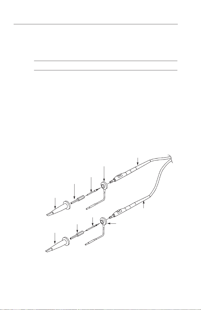
Probe Tip Replacement
NOTE. Both tips must be replaced at the same time.
Use the following procedure to change the probe tips (refer to
Figure 5–1).
1. Pull off the retractable hook tip.
2. Unscrew the tip cover.
3. Unscrew the installed tip.
4. Screw in the replacement tip.
5. If desired, screw on the tip cover and slide the retractable-hook
tip back into place.
Probe tip
Tip cover
Retractable
hook tip
Probe tip
Tip cover
Retractable
hook tip
Figure 5–1: P6135A probe tip assembly
5–2
Ground lead with
Cable
socket
Cable
Ground lead with socket
P6135A Instruction Manual
Page 61

Readjustment After Repair
Following any repair or parts replacement, complete the performance verification procedure (beginning on page 4-1) to verify that
the probe is within specification. If adjustment is necessary, follow
the appropriate procedure.
Instrument Repackaging for Shipment
If available, use the original packaging carton to ship your probe. If
the carton is unfit for use or not available, repackage the probe as
follows:
1. Use a carton with a test strength of no less than 175 pounds.
2. Surround the probe with protective polyethylene sheeting.
3. Cushion the probe on all sides with at least two inches of tightly
packed urethane foam or other packing material.
4. Seal the carton with shipping tape or an industrial stapler.
Maintenance
P6135A Instruction Manual
5–3
Page 62

Maintenance
5–4
P6135A Instruction Manual
Page 63

Replaceable Parts Replaceable Parts
Page 64

Page 65

Replaceable Parts
This section contains a list of the replaceable modules for the
P6135A differential probe pair. Use this list to identify and order
replacement parts.
Parts Ordering Information
Replacement parts are available through your local Tektronix field
office or representative.
Changes to T ektronix products are sometimes made to accommodate
improved components as they become available and to give you the
benefit of the latest improvements. Therefore, when ordering parts, it
is important to include the following information in your order:
H Part number
H Instrument type or model number
H Instrument serial number
H Instrument modification number, if applicable
If you order a part that has been replaced with a different or
improved part, your local T ektronix field office or representative will
contact you concerning any change in part number.
Change information, if any, is located at the rear of this manual.
Module Servicing
Modules can be serviced by selecting one of the following three
options. Contact your local T ektronix service center or representative
for repair assistance.
Module Exchange. In some cases you may exchange your module for a
remanufactured module. These modules cost significantly less than
new modules and meet the same factory specifications. For more
information about the module exchange program, call 1-800-TEKWIDE, extension 6630.
P6135A Instruction Manual
6–1
Page 66

Replaceable Parts
Module Repair and Return. You may ship your module to us for repair,
after which we will return it to you.
New Modules. You may purchase replacement modules in the same
way as other replacement parts.
Using the Replaceable Parts List
This section contains a list of the mechanical and/or electrical
components that are replaceable for the P6135A probe pair. Use this
list to identify and order replacement parts. The following table
describes each column in the parts list.
Parts list column descriptions
Column Column name Description
1 Figure & index number Items in this section are referenced by figure and
index numbers to the exploded view illustrations
that follow.
2 Tektronix part number Use this part number when ordering replacement
parts from Tektronix.
3 and 4 Serial number Column three indicates the serial number at
which the part was first effective. Column four
indicates the serial number at which the part was
discontinued. No entry indicates the part is good
for all serial numbers.
5 Qty This indicates the quantity of parts used.
6 Name & description An item name is separated from the description
by a colon (:). Because of space limitations, an
item name may sometimes appear as incom-
plete. Use the U.S. Federal Catalog handbook
H6-1 for further item name identification.
7 Mfr. code This indicates the code of the actual
manufacturer of the part.
8 Mfr. part number This indicates the actual manufacturer’s or
vendor’s part number.
6–2
P6135A Instruction Manual
Page 67

Replaceable Parts
Abbreviations
Abbreviations conform to American National Standard ANSI
Y1.1–1972.
Mfr. Code to Manufacturer Cross Index
The table titled Manufacturers Cross Index shows codes, names, and
addresses of manufacturers or vendors of components listed in the
parts list.
Manufacturers cross index
Mfr.
code
24931 BERG ELECTRONICS INC BERG ELECTRONICS
7X318 KASO PLASTICS INC 11013 A NE 39TH VANCOUVER, WA 98662
05006 20TH CENTURY BOK 3628 CRENSHAW
80009 TEKTRONIX INC 14150 SW KARL BRAUN DR
TK2469 UNITREK CORPORATION 3000 LEWIS & CLARK HWY
TK2548 XEROX CORPORATION 14181 SW MILLIKAN WAY BEAVERTON, OR 97005
TK2565 VISION PLASTICS INC 26000 SW PARKWAY
Manufacturer Address City, state, zip code
RF/COAXIAL DIV
2100 EARLYWOOD DR
PO BOX 547
BOULEVARD
ATTN: CUSTOM
DEPARTMENT
PO BOX 500
SUITE 2
CENTER DRIVE
FRANKLIN, IN 46131
LOS ANGELES, CA 90016
BEAVERT ON, OR
97077–0001
VANCOUVER, W A 98661
WILSONVILLE, OR 97070
P6135A Instruction Manual
6–3
Page 68

Replaceable Parts
8
7
11
6
5
14
12
13
9
10
6–4
4
3
2
1
Figure 6–1: P6135A probe with standard accessories
P6135A Instruction Manual
Page 69

Replaceable Parts
P6135A
Qty Name & description Mfr. code Mfr. part number
Serial no.
discont’d
Serial no.
effective
80009 013–0107–06
SIZE,RETRACTABLE HOOK ASSY
STANDARD ACCESSORIES
TK2469 196–3295–00
TK2565 344–0408–02
COLLAR
4230A,POLYPROPYLENE BLACK,PKG OF 12
Tektronix
part number
Fig. &
index
Replaceable parts: P6135A probe and standard accessories
number
6–1 –1 013–0107–06 9139 2 TIP,PROBE:MINIATURE/COMPACT
013–0107–07 9140 2 TIP,PROBE:MINIATURE/COMPACT SIZE TK2565 013–0107–07
–2 204–1049–00 2 BODY SHELL:TIP COVER TK2565 204–1049–00
–3 206–0415–00 1 TIP,PROBE:45–49PF,SET OF 2,BLUE/NATURAL 80009 206–0415–00
206–0416–00 1 TIP,PROBE:13–17 PF,SET OF 2,RED/NATURAL 80009 206–0416–00
206–0419–00 1 TIP,PROBE:18–22 PF,SET OF 2,BLACK/YELLOW 80009 206–0419–00
–4 196–3305–00 2 LEAD,ELECTRICAL:22 AWG,6.0 L,W/CLIP TK2469 196–3305–00
–5 343–1003–00 2 COLLAR,GND:P6130 80009 343–1003–00
–6 195–4240–00 2 LEAD,ELECTRICAL:0.025 DIA,COPPER,2.3 L TK2469 195–4240–00
–7 196–3113–02 2 LEAD,ELECTRICAL:STRD,22 AWG,6.0 L,8–N TK2469 196–3113–02
–8 016–0633–00 1 MARKER SET,CA:2 EA VARIOUS COLORS 80009 016–0633–00
–9 352–0670–00 2 HOLDER,PROBE:ATTENUATOR TIPS (3) TK2565 352–0670–00
–10 196–3295–00 1 LEAD,ELECTRICAL:22 AWG,6.0 L,8–N,W/DBL GRD
–11 344–0408–02 1 CLIP,RING,CABLE:S CLIP,TENITE
6–5P6135A Instruction Manual
Page 70

Replaceable Parts
Mfr. part numberMfr. codeName & descriptionQty
TK1163 003–1433–02
TOOL,PLASTIC,BLACK
Serial no.
discont’d
Serial no.
effective
Tektronix
part number
Fig. &
index
number
6–1 –12 016–0708–00 1 POUCH,ACCESSORY:6.25 X 9.25 05006 501494
Replaceable parts: P6135A probe and standard accessories (Cont.)
–13 003–1433–02 1 TOOL:SCREWDRIVER,ADJUSTMENT
6–6
070–7675–02 1 MANUAL,TECH:INSTR,P6135A,DP TK2548 070–7675–02
–14 206–0364–00 2 TIP,PROBE:MICROCKT TEST,0.05 CTR 80009 206–0364–00
P6135A Instruction Manual
Page 71

Replaceable Parts
78
6
5
9
4
10
3
11
2
1
12
13
Figure 6–2: P6135A probe optional accessories
6–7P6135A Instruction Manual
Page 72

Replaceable Parts
24931 28P264–2
24931 28P312–1
OPTIONAL ACCESSORIES
STRAIGHT THRU
ADAPTER
Qty Name & description Mfr. code Mfr. part number
Serial no.
discont’d
Serial no.
effective
Tektronix
part number
Fig. &
index
Replaceable parts: P6135A probe optional accessories
number
6–2 –1 013–0226–00 1 CONNECTOR,BNC:BNC TO PROBE TIP ADAPTER
–2 013–0227–00 1 CONNECTOR,BNC:50 OHM,BNC TO PROBE TIP
–3 131–5031–00 1 CONNECTOR,PROBE:PKG OF 25, COMPACT 80009 131–5031–00
–4 344–0398–00 1 CLIP,ELECTRICAL:ALLIGATOR,0.155 L,STL CS PL 80009 344–0398–00
–5 196–3113–03 1 LEAD,ELECTRICAL:STRD,22 AWG,3.0 L,8–N TK2469 196–3113–03
6–8
(SEE FIGURE 6–1–14)
– – – – – – – 1 SMT KLIPCHIP:20 ADAPTERS
–6 352–0351–00 1 HOLDER,PROBE:BLACK ABS P6000 SERIES 7X318 1127
P6135A Instruction Manual
Page 73

Mfr. part numberMfr. codeName & descriptionQty
Replaceable Parts
Serial no.
discont’d
Serial no.
effective
TK2565 013–0202–02
MINI
NOTE: ITEMS 8 THROUGH 12 ARE USABLE WHEN
THE SUBMINIATURE/COMPACT TO MINIATURE
PROBE TIP ADAPTER (FIGURE 6–2–7) IS USED.
24931 28P–302–2
TIP,MALE,STR,PROBE,2.14 L,INT 4.5 X 0.077 MM
THD,COMPACT
Tektronix
part number
Fig. &
index
number
Replaceable parts: P6135A probe optional accessories (Cont.)
6–2 –7 013–0202–02 1 ADAPTER,PROBE:SUBMINIATURE/COMPACT TO
015–0201–08 1 TIP,PROBE:IC TEST,PKG OF 100 80009 015–0201–08
–8 015–0201–07 1 TIP,PROBE:IC TEST,PKG OF 10 80009 015–0201–07
–9 017–0088–00 1 CONN,PLUG,ELEC:50 OHM,GR 80009 017–0088–00
–10 015–0325–00 1 ADAPTER,PROBE:PROBE TO CONNECTOR PINS TK2565 015–0325–00
–11 013–0085–00 1 TIP,PROBE:GROUNDING 80009 013–0085–00
–12 013–0084–01 1 ADAPTER,CONN:BNC TO PROBE 24931 28P156–1
–13 013–0254–00 1 ADAPTER,CONN:BNC TO PROBE
6–9P6135A Instruction Manual
Page 74

Replaceable Parts
6–10
P6135A Instruction Manual
 Loading...