

Page 1

xx
P5960
High-Density D-MAX Probe
ZZZ
for TLA6400 Series Logic Analyzers
Instruction Manual
Revision A
Warning
The servicing instructions are for use by qualified personnel
only. To avoid personal injury, do not perform any servicing
unless you are qualified to do so. Refer to all safety summaries
prior to performing service.
www.tektronix.com
P077063700*
*
077-0637-00
Page 2

Copyright © Tektronix. All rights reserved. Licensed software products are owned by Tektronix or its subsidiaries
or suppliers, and are protected by national copyright laws and international treaty provisions.
Tektronix products are c overed by U.S. and foreign patents, issued and pending. Information in this publication
supersedes that in all previously published material. Specifications and price change privileges reserved.
TEKTRONIX and TEK are registered trademarks of Tektronix, Inc.
D-Max is a registered trademark of Tektronix, Inc. MagniVu is a trademark of Tektronix, Inc.
cLGA is a registered trademark of Amphenol Intercon Systems, Inc.
Velcro is a registered trademark of Velcro Industries B.V.
Contacting Tektronix
Tektro ni
14150 SW Karl Braun Drive
P.O . Bo x 5 00
Beaverton, OR 97077
USA
For pro
x, Inc.
duct information, sales, service, and t echnical support:
In North America, call 1-800-833-9200.
World wi d e, visi t www.tektronix.com to find contacts in your area.
Page 3

Warranty
Tektronix warrants that this product will be free from defects in materials and workmanship for a period of one (1)
year from the date of shipment. If any such product proves defective during this warranty period, Tektronix, at its
option, either will repair the defective product without charge for parts and labor, or will provide a replacement
in exchange for the defective product. Parts, modules and replacement products used by Tektronix for warranty
work may be n
the property of Tektronix.
ew or reconditioned to like new performance. All replaced parts, modules and p roducts become
In order to o
the warranty period and make suitable arrangements for the performance of service. Customer shall be responsible
for packaging and shipping the defective product to the service center designated by Tektronix, with shipping
charges prepaid. Tektronix shall pay for the return of the product to Customer if the shipment is to a location within
the country in which the Tektronix service center is located. Customer shall be responsible for paying all shipping
charges, duties, taxes, and any other charges for products returned to any other locations.
This warranty shall not apply to any defect, failure or damage caused by improper use or improper or inadequate
maintenance and care. Tektronix shall not be obligated to furnish service under this warranty a) to repair damage
result
b) to repair damage resulting from improper use or connection to incompatible equipment; c) to repair any damage
or malfunction caused by the use of non-Tektronix supplies; or d) to service a product that has been modified or
integrated with other products when the effect of such modification or integration increases the time or difficulty
of servicing the product.
THIS WARRANTY IS GIVEN BY TEKTRONIX WITH RESPECT TO THE PRODUCT IN LIEU OF ANY
OTHER WARRANTIES, EXPRESS OR IMPLIED. TEKTRONIX AND ITS VENDORS DISCLAIM ANY
IMPLIED WARRANTIES OF MERCHANTABILITY OR FITNESS FOR A PARTICULAR PURPOSE.
TRONIX' RESPONSIBILITY TO REPAIR OR REPLACE DEFECTIVE PRODUCTS IS THE SOLE
TEK
AND EXCLUSIVE REMEDY PROVIDED TO THE CUSTOMER FOR BREACH OF THIS WARRANTY.
TEKTRONIX AND ITS VENDORS WILL NOT BE LIABLE FOR ANY INDIRECT, SPECIAL, INCIDENTAL,
OR CONSEQUENTIAL DAMAGES IRRESPECTIVE OF WHETHER TEKTRONIX OR THE VENDOR HAS
ADVANCE NOTICE OF THE POSSIBILITY OF SUCH DAMAGES.
[W2 – 15AUG04]
btain service under this warranty, Customer must notify Tektronix of the defect before the expiration of
ing from attempts by personnel other than Tektronix representatives to install, repair or service the product;
Page 4

Page 5

Table of Contents
General safety summary ................ .................................. ................................ ......... v
Service safety summary.......................................................................................... vii
Compliance information ......................................................................................... viii
Environmental considerations .............................................................................. viii
Preface.............................................................................................................. ix
Related documentation ................................. ................................ ...................... ix
Operating basics ........................... ................................ .................................. ....... 1
Product description ......... ................................ ................................ ................... 1
P5960 probe accessory information ......................................................................... 2
Probe label overview ................. ................................ ................................ ......... 3
Apply the labels to the probe.... ................................ .................................. ........... 5
Probe connection overview ................................................................................... 7
Probe head handling guidelines .............................................................................. 7
Connect the probe to the instrument .............................. ................................ ........... 9
Connect the probes to the SUT................ .................................. ............................. 9
Dress the probe cables........................................................................................ 11
Store the probe head when not in use......................................... .............................. 12
Probe connection troubleshooting guidelines........................................ ...................... 12
Reference ....... ................................ ................................ .................................. .. 15
Clocks and qualifiers ... ................................ ................................ ...................... 15
Multiplexed buses . . .... .. ... . .... .. ... . .... .. ... . .... .. ... . .... .. ... . .... .. ... . .... .. ... . .... .. ... . .... .. ... . 16
High-Resolution timing ...................................................................................... 17
Range recognizers ...... ................................ .................................. .................... 17
Probe dimensions ............... .................................. ................................ ............ 18
Retention assembly dimensions and keepout areas ....... ................................ ................ 18
Retention assembly side-by-side and end-to layout dimensions......................................... 20
Retention post dimensions and keepout areas ............................................................. 20
Retention post side-by-side and end-to-end layout dimensions ......................................... 22
Signal routing ..................... ................................ .................................. .......... 23
Mechanical considerations................................................................................... 23
Electrical considerations ..................................................................................... 23
Probe footprint dimensions ................ ................................ ................................ .. 24
Via-in-Pad design considerations ........................................................................... 25
Probe pinout definition a nd channel assignment . . ... . ... . .... .. ... . ... . ... . ... . . . ... . ... . ... . ... . .... .. .. 27
Specifications...... ................................ ................................ ............................ 29
Maintenance........................................................................................................ 31
Probe calibration information ................... .................................. .......................... 31
Probe service strategy information.......................................................................... 31
Perform the functional check...... ................................ .................................. ........ 31
P5960 Logic Analyzer Probe Instruction Manual i
Page 6

Table of Contents
Inspect or clea
Replace the cLGA clip ....................................................................................... 32
Repackage the probe ............... ................................ ................................ .......... 33
Replaceable parts .......................... ................................ ................................ ........ 35
Parts ordering information......... .................................. ................................ ........ 35
Appendix A: Probe retention assembly installation information............. ................................ 37
Clean the co
Install the probe retention assembly ........................................................................ 37
Retention post information .......... .................................. ................................ ...... 38
Replace the retention post wires .... ................................ ................................ ........ 39
Install the retention posts on the PCB .......................... ................................ ............ 39
Glossary
Index
n the probe.................................................................................... 32
mpression footprints on the SUT..................... .................................. ...... 37
ii P5960 Logic Analyzer Probe Instruction Manual
Page 7

List of Figures
Figure 1: P5960 High-Density probe with D-Max probing technology...................................... 1
Figure 2: P5960 probe label sheet. ............................................................................... 4
Figure 3: Attaching labels to the P5960 probe .................................................................. 6
Figure 4: Pr
Figure 5: Storing the probe head.................................................................................. 8
Figure 6: Connecting the logic analyzer probe.................................................................. 9
Figure 7: Connecting the probes to the SUT ................................................................... 10
Figure 8: Proper dressing of the probe cables.................. ................................ ................ 11
Figure 9: Protecting the probe head ... ................................ ................................ .......... 12
Figure 1
Figure 11: Retention assembly dimensions..................................................................... 19
Figure 12: Retention assembly keepout area... ................................ ................................ 19
Figure 13: Retention assembly side-by-side layout........ ................................ .................... 20
Figure 14: Retention assembly end-to-end layout ............................................................. 20
Figure 15: Retention posts dimensions ......................................................................... 21
re 16: Retention posts keepout area ........................................................................ 21
Figu
Figure 17: Retention posts side-by-side layout ................................................................ 22
Figure 18: Retention posts end-to-end layout .................................................................. 22
Figure 19: Signal routing on the SUT....................... ................................ .................... 23
Figure 20: High-Density probe load model..................................................................... 24
Figure 21: Probe footprint dimensions on the PCB............................................................ 25
gure 22: Optional Via-in-Pad placement recommendation ............................. .................... 26
Fi
Figure 23: P5960 single-ended PCB footprint pinout detail.................................................. 27
Figure 24: Replacing the cLGA clip .................... .................................. ...................... 33
Figure 25: Installing the probe retention assembly ... .. ... . .... .. ... . ... . .... .. ... . ... . . . ... . ... . . . ... . ... . ... 38
Figure 26: Replacing the wires on the retention posts......................................................... 39
Figure 27: Installing the retention posts on the PCB . . .... .. ... . ... . . . ... . ... . .... .. ... . ... . . . ... . ... . . . ... . .. 40
Figure 28: Soldering the retention posts on the PCB........ ................................ .................. 41
oper handling of the interface clip.................................................................. 7
0: P5960 probe dimensions............................................................................. 18
P5960 Logic Analyzer Probe Instruction Manual iii
Page 8

Table of Contents
List of Tables
Table 1: Probe section and label combinations.................................................................. 3
Table 2 : Log
Table 3: Half channel demultiplexing source-to channel assignments . .. ... . .... .. ... . ... . .... .. ... . ... . ... 16
Table 4: Channel assignment for a P5960 single-ended logic analyzer probe.............................. 27
Table 5: Mechanical and electrical specifications...................................... ........................ 29
Table 6: Environmental specifications .............. .................................. .......................... 29
Table 7: Service options ............ ................................ ................................ .............. 31
ic analyzer clock and qualifier availability .. .. ... . ... . .... .. ... . ... . .... . . ... . ... . ... . . . ... . ... . 15
iv P5960 Logic Analyzer Probe Instruction Manual
Page 9

General safety summary
General safet
To avoid fire or personal
injury
y summary
Review the fo
this product or any products connected to it.
To avoid pot
Only qualified personnel should perform service procedures.
While using this product, you may need to access other parts of a larger system.
Read the safety sections of the other component manuals for warnings and
cautions r
Connect and disconnect properly. Connect the probe output to the measurement
instrument before connecting the probe to the circuit under test. Connect the
probe reference lead to the circuit under test before connecting the probe input.
Disconnect the probe input and the probe reference lead from the circuit under test
before
Ground the product. This product is indirectly grounded through the grounding
condu
conductor must be connected to earth ground. Before making connections to
the input or output terminals of the product, ensure that the product is properly
grounded.
disconnecting the probe from the measurement instrument.
ctor of the mainframe power cord. To avoid electric shock, the grounding
llowing safety precautions to avoid injury and prevent damage to
ential hazards, use this product only as specified.
elated to operating the system.
Observe all terminal ratings. To avoid fire or shock hazard, observe all ratings
and markings on the product. Consult the product manual for further ratings
information before making connections to the product.
The inputs are not rated for connection to mains or Category II, III, or IV circuits.
Do not apply a potential to any terminal, including the common terminal, that
exceeds the maximum rating of that terminal.
Power disconnect. The power cord disconnects the product from the power source.
Do not block the power cord; it must remain accessible to the user at all times.
Do not operate without covers. Do not operate this product with covers or panels
removed.
Do not operate with suspected failures. If you suspect that there is damage to this
product, have it inspected by qualified service personnel.
Avoid exposed circuitry. Do not touch exposed connections and components when
power is present.
Use proper fuse. Use only t he fuse type and rating specified for this product.
P5960 Logic Analyzer Probe Instruction Manual v
Page 10

General safety summary
Termsinthismanual
Symbols and terms on the
product
Do not operate i
Do not operate in an explosive atmosphere.
Keep product surfaces clean and dry.
Provide prop
on installing the product s o it has proper ventilation.
These terms may appear in this manual:
WARNING.
in injury or loss of life.
CAUTION
damage to this product or other property.
These t
erms may appear on the product:
DANGER indicates an injury hazard immediately accessible as you read
the ma
n wet/damp conditions.
er ventilation. Refer to the manual's installation instructions for details
Warning statements identify conditions or practices that could result
. Caution statements identify conditions or practices that could result i n
rking.
WARNING indicates an injury hazard not immediately accessible as you
the marking.
read
CAUTION indicates a hazard to property including the product.
The following symbol(s) may appear on the product:
vi P5960 Logic Analyzer Probe Instruction Manual
Page 11

Service safety summary
Service safet
ysummary
Only qualifie
safety summary and the General safety summary before performing any service
procedures.
Do not service alone. Do not perform internal service or adjustments of this
product unless another person capable of rendering first aid and resuscitation is
present.
Disconnect power. To avoid electric shock, switch off the instrument power, then
disconnect the power cord from the mains power.
Use care when servicing with power on. Dangerous voltages or currents may exist
in this p
test leads before removing protective panels, soldering, or replacing components.
To avoi
d personnel should perform service procedures. Read this Service
roduct. Disconnect power, remove battery (if applicable), and disconnect
d electric s hock, do not touch exposed connections.
P5960 Logic Analyzer Probe Instruction Manual vii
Page 12

Compliance information
Compliance in
formation
This section
environmental standards with which the instrument complies.
Environmental considerations
This section provides information about the environmental impact of the product.
Product end-of-life
handling
Observe the following guidelines when recycling an instrument or component:
Equipment recycling. Production of this equipment required the extraction and
use of natural resources. The equipment may contain substances that could be
harmful to the environment or human health if improperly handled at the product’s
end of life. To avoid release of such substances into the environment and to
reduce the use of natural resources, we encourage you to recycle this product in
an appr
recycled appropriately.
opriate system that will ensure that most of the materials are reused or
lists the EMC (electromagnetic compliance), safety, and
This symbol indicates that this product complies w ith the applicable European
Union requirements according to Directives 2002/96/EC and 2006/66/EC
on waste electrical and electronic equipment (WEEE) and batteries. For
information about recycling options, check the Support/Service section of the
Tektronix Web site (www.tektronix.com).
Restriction of hazardous
tances
subs
This product is classified as Monitoring and Control equipment, and is outside the
pe of the 2002/95/EC RoHS Directive.
sco
viii P5960 Logic Analyzer Probe Instruction Manual
Page 13

Preface
Related documentation
This document provides information on using and servicing the P5960 logic
analyzer probe.
The following list and table provide information on the related documentation
available
for your Tektronix product. For additional information, refer to the
Tektronix Web site (www.tektronix.com/manuals).
Related documentation
Item Purpose
TLA Quick Start User Manuals
Online Help
Installation Reference Sheets High-level installation information
lation Manuals
Instal
XYZs of Logic Analyzers
Declassification and Securities instructions Data security concerns specific to sanitizing
Application notes
Product Specifications & Performance
Verification Procedures
TPI.NET Documentation
Field upgrade kits
ptional Service Manuals
O
High-lev
In-dept
Detailed first-time installation information
Logic a
or removing memory devices from Tektronix
prod
Coll
specific notes
TLA Product specifications and performance
verification procedures
Detailed information for controlling the logic
an
Up
S
mainframes
el operational overview
h operation and UI help
nalyzer basics
ucts
ection of logic analyzer application
alyzer using .NET
grade information for your logic analyzer
elf-service documentation for modules and
P5960 Logic Analyzer Probe Instruction Manual ix
Page 14

Preface
x P5960 Logic Analyzer Probe Instruction Manual
Page 15

Operating basics
Product description
This section provides a b rief description of the Tektronix P5960 High-Density
Logic Analyzer Probe, information on attaching color-coded p robe labels, and
probe and ada
The P5960 Probe is a 34-channel, high-density connectorless probe with D-Max
probing technology.
The P5960 Probe consists of one probe head that has 34 channels (32 data and 2
clock/qual). (See Figure 1.)
pter connection instructions from the logic analyzer to the SUT.
Figure 1: P5960 High-Density probe with D-Max probing technology
The following list details the capabilities and qualities of the P5960 probe:
Single-ended data and single-end
cLGA contact eliminates need for built-in connector
Footprint supports direct signal pass-through
Supports PCB thickness of 1.27 mm to 6.35 mm (0.050 in to 0.250 in)
Consists of one independent probe head of 34 channels (32 data and 2
clock/quals), and two 17-channel logic analyzer-end connectors.
Half channel demux mode, (for example, 1:2 demultiplexing) uses one-half
of the probe head
P5960 Logic Analyzer Probe Instruction Manual 1
ed clock inputs
Page 16

Operating basics
Color-coded ke
-2.5 V to +5 V input operating range
300 mV minimum single-ended signal amplitude
Minimal loading of 20 kΩ, 0.8 pF to ground
P5960 probe accessory information
The P5960 probe includes accessories to connect the logic analyzer to the SUT.
The following accessories are available for the P5960 probe:
Component kit cLGA interface clip kit (Tektronix part number, 020-2622-xx)
Primary p
tworetentionassemblysocketsandmanual
Probe la
P5960 Logic Analyzer Probe Instructions (Tektronix part number,
071-29
P5960 High-Density Logic Analyzer Probe Instruction Manual (Tektronix
part n
downloadable from the Tektronix Web site: www.tektronix.com/manuals)
robe retention kit (Tektronix part number, 020-2908-xx); includes
bels, one sheet (Tektronix part number, 335-2737-xx)
76-xx)
umber, 077-0637-xx, available on the TLA Documentation CD or
yed attachment
2 P5960 Logic Analyzer Probe Instruction Manual
Page 17

Probe label overview
Operating basics
The logic analyzer probe comes with a sheet of labels to apply to the probe before
connecting the probe to the instrument and SUT.
When you purchase the logic analyzer probe, apply the color-coded labels as
described in this section. The labels help you identify the probe connections at the
logic analyzer end and at the SUT end.
The following table lists the probe section and label color combinations. Refer to
the table when you attach the probe labels.
Table 1: Probe section and label combinations
Probe
section Channels
A3-A2
D3-D2
C3-C2 CK3,
E3-E2
CK0,
A3:7-0,
A2:7-0
QUAL0,
D3:7-0,
D2:7-0
C3:7-0,
C2:7-0
QUAL3,
E3:7-0,
E2:7-0
Label
color
Brown A1-A0
Blue D1-D0
White
Green
Probe
section Channels
C1-C0 QUAL1,
E1-E0
CK1,
A1:7-0,
A0:7-0
CK2,
D1:7-0,
D0:7-0
C1:7-0,
C0:7-0
QUAL2,
E1:7-0,
E0:7-0
Label
color
Orange
Yellow
Gray
Violet
P5960 Logic Analyzer Probe Instruction Manual 3
Page 18

Operating basics
The following fi
gure shows a sample probe label sheet.
Figure 2: P5960 probe label sheet.
4 P5960 Logic Analyzer Probe Instruction Manual
Page 19

Apply the labels to the probe
Attach the labels to the logic analyzer-end of the probe and to both sides of the
probe head.
NOTE. Use flat-nosed tweezers to remove the labels from the sheet of labels.
Never peel labels with your fingers. The labels are made of soft vinyl and can
stretch and
right corner while removing it from the sheet of labels.
Operating basics
distort easily. To avoid stretching the label, always hold it from the top
The adhesi
the intended outline on the logic analyzer-end and probe head before attaching it
to the probe. Once labels are placed on the probe, they become very difficult to
remove.
Use the following steps to attach the probe labels:
1. Identify the logic analyzer-ends of the probes.
The side of the probe that contains a black label has an area for the color-coded
label.
NOTE. Note the indents and the outdents on the probe labels. Use the indents and
outd
2. From the sheet of labels, locate the color-coded label for the logic analyzer
end
3. Locate the probe head and attach the matching colored label to the probe
he
4. Turn the probe over and repeat Step 3 to apply the other labels to the probe
as
ve on the vinyl labels is extremely s trong. Carefully align each label to
ents as guides to position the labels on the probes. (See Figure 3 on page 6.)
of the probe cable and attach it to the logic analyzer probe connector.
ad.(See Figure 3 on page 6.)
shown in the illustration.
P5960 Logic Analyzer Probe Instruction Manual 5
Page 20

Operating basics
Figure 3: Attaching labels to the P5960 probe
6 P5960 Logic Analyzer Probe Instruction Manual
Page 21

Probe connection overview
The P5960 probe connects a TLA6400 Series logic analyzer to probe retention
assemblies installed on the circuit board on the SUT.
If the retention assemblies are not already installed on the SUT, refer to the
procedures for installing the retention assemblies. (See page 37, Probe retention
assembly installation information.)
Probe head handling guidelines
The cLGA interface clip in the probe head should always be handled with care.
Use the following guidelines when you handle the probe head and cLGA interface
clip:
Always handle the cLGA interface clip by the outer edges, and be careful to
avoid the contacts in the center. Do not touch the contacts with your fingers,
tools, wipes, or any other devices. (See Figure 4.)
Operating basics
Figure 4: Proper handling of the interface clip
Do not expose the connector to liquids or dry chemicals.
If the board pad array needs to be cleaned, only use isopropyl alcohol and
lint-free cloth. (See page 37, Clean the compression footprints on the SUT.)
Immediately following cleaning, or immediately prior to placement of
connector to circuit board, blow off the board pad array and connector contact
array with clean, oil-free dry air or nitrogen to remove loose debris. First start
P5960 Logic Analyzer Probe Instruction Manual 7
Page 22

Operating basics
the blowing pro
across the pad and contact arrays in a repeated motion to remove loose debris.
Place the conn
for alignment. Use care to prevent incidental contact with other surfaces or
edges in the connector contact array area prior to board placement.
Always store the probe head in the protective cover when not in use. (See
Figure 5.)
cess by aiming away from the array areas, and then sweep
ector onto the board pad array using the bosses or locator p ins
Figure 5: Storing the probe head
8 P5960 Logic Analyzer Probe Instruction Manual
Page 23

Operating basics
Connect the pr
obe to the instrument
The P5960 probe connects a TLA6400 Series logic analyzer to the SUT. You can
connect the P5960 probe to the SUT without turning off the power to the SUT.
Apply the labels to the probes before connecting the probes to the instrument
andtotheSUT.
1. Match the color-coded labels of the probe to the same color-coded connector
on the logic analyzer.
2. Connect the logic analyzer probe as shown. The probe will latch into place.
To disconnect the probe, press the button at the center of the probe to release
the latch and then pull the probe away from the logic analyzer.
Figure 6: Connecting the logic analyzer probe
Connect the probes to the SUT
e probe heads connect to the retention assembly on the SUT.
Th
Verify that one or more retention assemblies are installed on the SUT before you
tempt to connect the probes. If they are not installed refer to the instructions for
at
installing them. (See page 37, Install the probe retention assembly.)
P5960 Logic Analyzer Probe Instruction Manual 9
Page 24

Operating basics
Connect the pro
1. Align the silver screw on the probe to the silver side of the retention assembly.
bes to the SUT using the following steps.
Figure 7: C onnecting the probes to the SUT
2. Start both screws in the retention assembly, and tighten them evenly
(approximately 1 in-lb) to make sure that the probe approaches and mates
squarely to the circuit board.
ION. When attaching the probe head to the target system, use care to evenly
CAUT
tighten probe head screws until they are snug. First tighten both screws until the
nut bar makes contact with the circuit board surface, then snug each screw to 1
in-lb (max). Under-tightening the probe head screws can result in intermittence.
Over-tightening can result in damage to the cLGA clip and s tripped screws.
If access is limited, use the adjustment tool that came with your probe. The
probe is completely fastened when the screws stop in the assembly.
10 P5960 Logic Analyzer Probe Instruction Manual
Page 25

Dress the probe cables
Operating basics
Use the Velcro cable managers to combine the cables together or to help relieve
strain on the probe connections.
Hang the probe cables so that you relieve the tension on the probes at the retention
posts as shown in the following figure.
Figure 8: Proper dressing of the probe cables
P5960 Logic Analyzer Probe Instruction Manual 11
Page 26

Operating basics
Store the prob
e head when not in use
To protect the interface clip, it is important to properly store the probe head when
the probe is not in use. Use the protective cover as shown in the following figure.
Figure 9: Protecting the probe head
Probe connection troubleshooting guidelines
Refer to the guidelines in this section to identify probe connection problems.
The most obvious symptom of a p roblem with the probe installation is seeing
incorrect data in the logic analyzer acquisition. The nature of the incorrect data
has a very consistent characteristic; the data from multiple channels go to a logic
low and stay there. Intermittent bad data, or a single dead channel are not failures
typically associated with probe installation problems.
Slightly move the probe head to either side, or press down on the probe head
while making new acquisitions.
If good data is now being acquired, then the probe mounting is most likely
the cause.
If good data is not acquired, then remove the probe and check the retention
assemblyfortoomuchplay.
If there is significant play, then the probe mounting is most likely the cause.
12 P5960 Logic Analyzer Probe Instruction Manual
Page 27

Operating basics
If the retentio
the bottom of the assembly and the circuit board surface, then move the probe
with bad data f rom one logic analyzer probe location to another.
If the problem follows the probe, then the probe is the problem.
Visu a lly in
missing c-spring metal contacts.
Ifthereisd
missing, replace the cLGA interface clip. (See page 32, Replace the cLGA
clip.)
If the problem does not follow the probe, it is either the logic analyzer or the
probe connection at its previous location.
Move the probe back to the original location to be certain it was not a
connection problem at the logic analyzer end.
Place another probe in the retention assembly of the original probe. If the new
probe acquires data, then the old probe is probably at fault.
n assembly has m inimal play and you cannot see a gap between
spect the cLGA interface clip on the probe for any damage or
amage to the interface clip, or if any c-spring metal contacts are
P5960 Logic Analyzer Probe Instruction Manual 13
Page 28

Operating basics
14 P5960 Logic Analyzer Probe Instruction Manual
Page 29

Reference
Clocks and qualifiers
This section provides reference information for the P5960. After you have
determined which probe is required, use the information in this section to design
the appropri
ate connector into your SUT circuit board.
Use the clo
logic analyzer stores data.
Every log
as clocks can cause the logic analyzer to store data. Qualifier channels can be
logically ANDed and ORed with clocks to further define when the logic analyzer
should latch data from the SUT. Routing the appropriate signals from your design
to these inputs ensures that the logic analyzer can acquire data correctly. Unused
clocks can be used as qualifi er signals.
Depending on the channel width, each TLA6400 Series logic analyzer will have a
different set of clock and qualifier channels. The following table shows the clock
and qu
Table 2: Logic analyzer clock and qualifier availability
Product
TLA6401 X X
TLA6402 XXXX
TLA6403 XXXXXX
TLA6404 XXXXXXXX
Clock inputs Qualifier inputs
CLK:0 CLK:1 CLK:2 CLK:3 QUAL:0 QUAL:1 QUAL:2 QUAL:3
ck and qualifier probe connections from the SUT to define how the
ic analyzer has some special purpose input channels. Inputs designated
alifier channels available for each instrument.
All clock and qualifier channels are stored. The logic analyzer always stores the
logic state of these channels every time it latches data.
Since clock and qualifier channels are stored in the logic analyzer memory, there
is no need to double probe these signals for timing analysis. When switching
from state to timing analysis, all of the clock and qualifier signals are visible.
This allows you to route signals not needed for clocking to the unused clock
and qualifier channels.
It is a g ood practice to take advantage of the unused clock and qualifier channels
to increase your options for when you will latch data. Routing several clocks and
strobes in your design to the logic analyzer clock inputs will provide you with a
greater flexibility in the logic analyzer Setup menu.
P5960 Logic Analyzer Probe Instruction Manual 15
Page 30

Reference
Multip
lexed buses
As an example, l
ook at a processor with a master clock, data strobe, and an
address strobe. Routing all three of these signals to logic analyzer clock inputs
will enable you to latch data on the processor master clock, only w hen data is
strobed, or only when address is strobed. Some forethought in signal routing can
greatly expand the ways to latch and analyze data.
A processor also provides a good example of signals that can be useful as
qualifiers. There are often signals that indicate data reads versus data writes
(R/W), signals that show when alternate bus masters have control of the processor
buses (DMA
), and signals that show when various memory devices are being
used (ChipSe l). All of these signals are good candidates for assignment to
qualifier channels.
By logically ANDing the clock with one of these qualifiers you can p rogram the
logic analyzer to store only data reads or data writes. Using the DMA signal as a
qualifier provides a means of filtering out alternate bus master cycles. Chip selects
can limit data latching to specific memory banks, I/O ports, or peripheral devices.
TLA6400 Series logic analyzers support half channel demultiplexing.
Each signal on a dual multiplexed bus can be demultiplexed into its own logic
analyzer channel. See the following table to determine the correct channel groups
to use.
le 3: Half channel demultiplexing source-to channel assignments
Tab
Destination channels receiving SUT test dataSource
connecting
nnel
cha
groups TLA6404 TLA6403 TLA6402 TLA6401
:7-0
A3
A2:7-0 D2:7-0 D2:7-0
A1:7-0 D1:7-0 D1:7-0 D1:7-0
0:7-0
A
3:7-0
C
C2:7-0 C0:7-0 C0:7-0
E3:7-0 E1:7-0
E2:7-0 E0:7-0
D3
D
C
:7-0
0:7-0
1:7-0
D3
D
C
:7-0
0:7-0
1:7-0
0:7-0
D
A3:7-0 A3:7-0
A2:7-0 A2:7-0
When demultiplexing data there is no need to connect the destination channels to
the multiplexed bus. Data from the source channels are routed to the destination
channels internal to the logic analyzer.
16 P5960 Logic Analyzer Probe Instruction Manual
Page 31

Reference
High-Resolution timing
Range r
ecognizers
Demultiplexin
means that the MagniVu memory is filled with data from whatever is connected to
the demultiplexing destination channel probe inputs. This provides an opportunity
to acquire high resolution MagniVu data on a few extra channels. Connecting the
demultiplexing destination channels to other signals will allow viewing of their
activity in the MagniVu memory but not the main memory.
The high-resolution timing mode provides double the normal 800 MHz sample
rate on one
channels can be sampled at a 1.6 GHz rate with double the memory depth.
Obtain ex
signals to the demultiplexing source channels. Since demultiplexing affects only
the main memory you will still have the MagniVu data available for all of the
signals that are disconnected from the main memory when you switch to the
high resolution timing modes.
g affects only the main memory for the destination channels. This
-half of the channels. By trading half of the channels, the remaining
tra timing resolution where it is most needed by assigning critical
When using range recognizers, the probe groups and probe channels must be
in hardware order.
Probe groups must be used from the most-significant probe group to the
least-significant probe group based on the following order:
C3 C2 C1 C0 E3 E2 E1 E0 A3 A2 D3 D2 A1 A0 D1 D0 Q3 Q2 Q1 Q0
CK3 CK2 CK1 CK0
Probe channels must be from the most-significant channel to the least-significant
channel based on the following order:
76543210
The above examples assumes a 136-channel logic analyzer. The missing channels
in logic analyzers with fewer than 136 channels are ignored.
P5960 Logic Analyzer Probe Instruction Manual 17
Page 32

Reference
Probe dimensions
The following figure shows the dimensions for the P5960 probe.
Figure 10: P5960 probe dimensions
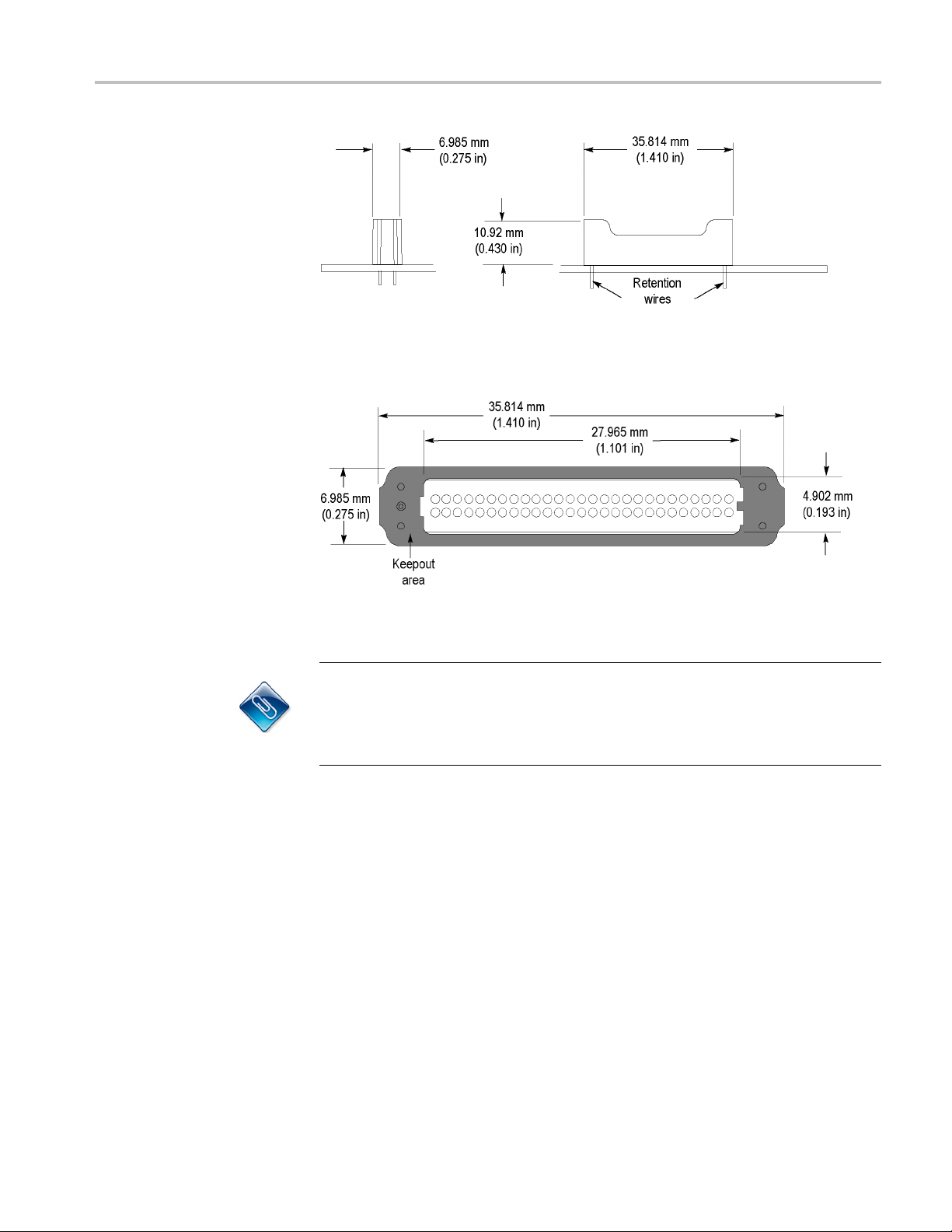
Retention assembly dimensions and keepout areas
The retention assembly provides a housing around the probe connector footprint
to stabilize the probe. The following figure shows the dimensions of the retention
assembly. All dimensions are per standard IPC tolerance, which is ±0.004 in.
(See Figure 11.)
UTION. To avoid solder creep, bend the assembly wires out after you insert the
CA
wires in the board, and then solder the wires.
18 P5960 Logic Analyzer Probe Instruction Manual
Page 33
Reference
Figure 11: Retention assembly dimensions
The following figure shows the keep out area required for the retention assembly.
Figure
NOTE. Tektronix has provided a 3D CAD solid model file (named
dmax_
footprint information for your circuit board. The file is attached to this PDF file.
To access the attached file, open the PDF fileandclickonthepaperclipiconon
theleftsideofthedocumentviewer.
12: Retention assembly keepout area
socket_assembly.stp) for the plastic retention assembly. It also includes
P5960 Logic Analyzer Probe Instruction Manual 19
Page 34

Reference
Retention assembly side-by-side and end-to layout dimensions
The following figure shows the dimensions for side-by-side footprint layout.
(See Figure 17.)
Figure 13: Retention assembly side-by-side layout
The following figure shows the dimensions for an end-to-end footprint layout.
Figure 14: Retention assembly end-to-end layout
Retention post dimensions and keepout areas
Retention posts provide another means for attaching the probes to the PCB.
etention posts hold the probe securely to the board, and ensure a reliable
the r
electrical and mechanical connection and pin-to-pad alignment to your design.
Board thicknesses that are supported include 1.27 mm (0.050 in) to 6.35 mm
(0.250 in). The dimensions of the retention posts are shown in the following
figure. (See Figure 15.)
All dimensions are per standard IPC tolerance, which is ±0.004 in.
CAUTION. To avoid solder creep, bend the post wires out after you insert the posts
in the board, and then solder the post wires. You can solder the retention wires
rom the top or bottom of the circuit board.
f
20 P5960 Logic Analyzer Probe Instruction Manual
Page 35

Reference
Figure 15: Retention posts dimensions
The following figure shows the keepout area required for the retention posts. (See
Figure 16.) Vias m ust be placed outside of the keepout area. Any traces routed on
the top layer of the board must stay outside of the keepout area. Traces can be
routed on inner layers of the board through the keepout area.
Figure 16: Retention posts keepout area
P5960 Logic Analyzer Probe Instruction Manual 21
Page 36

Reference
Retention post side-by-side and end-to-end layout dimensions
The following figure shows the dimensions for side-by-side footprint layout.
(See Figure 17.)
Figure 17:
The follo
(See Figure 18.)
Figure 18: Retention posts end-to-end layout
wing figure shows the dimensions for an end-to-end footprint layout.
Retention posts side-by-side layout
22 P5960 Logic Analyzer Probe Instruction Manual
Page 37

Reference
Signal routin
g
The following figure shows examples of pass-through signal routing for a
single-ended data configuration.
Figure 19: Signal routing on the SUT
Mechanical considerations
The PCB holes, in general, do not have an impact upon the integrity of your
signals when the signals routed around the holes have the corresponding return
current plane immediately below the signal trace for the entire signal path from
driver to receiver.
NOTE. For optimum signal integrity, there should be a continuous, uninterrupted
ground return plane along the entire signal path.
Electrical considerations
Load models are important electrical considerations when working with the probe.
The compression land pattern pad is not part of the load model. Make sure that
you include the compression land pad in the modeling.
Transmission lines
Due to the high performance nature of the interconnect, make sure that stubs,
which are greater than 1/4 length of the signal rise time, are modeled as
transmission lines.
P5960 Logic Analyzer Probe Instruction Manual 23
Page 38

Reference
P5960 probe load model
The following e
High-Density Single-Ended Probe.
Figure 20: High-Density probe load model
Probe footprint dimensions
Use the probe footprint dimensions to lay out your circuit board pads and holes
for attaching the retention posts.
(See Figure 21 on page 25.) If you are using the alternate retention assembly, all
dimensions remain the same as shown below, except the overall length and width.
(See Figure 11 on page 19.) Pad finishes that are supported include immersion
gold, immersion silver, and hot air solder level.
All dimensions are per standard IPC tolerance, which is ±0.004 in.
lectrical model includes a low-frequency model of the
NOTE. Tektronix recommends using immersion gold surface finish for best
rmance.
perfo
Tektronix also recommends that the probe attachment holes float or remain
nnected to a ground plane. This prevents overheating the ground plane
unco
and promotes quicker soldering of the retention posts to your PCB. The probe
retention posts are designed to allow you to solder the retention posts from either
side of your PCB.
NOTE. Tektronix has provided a 3D CAD solid model file (named
dmax_socket_assembly.stp) for the plastic retention assembly. It also includes
footprint information for your circuit board. The file is attached to this PDF file.
To access the attached file, open the PDF file and click on the paperclip icon on
he left side of the document viewer.
t
24 P5960 Logic Analyzer Probe Instruction Manual
Page 39

Reference
Figure 21: Probe footprint dimensions on the PCB
NOTE. Maintain a solder mask web between the pads when traces are routed
between pads on the same layer. The solder mask must not encroach onto the pads
within the pad dimensions. (See Figure 16 on page 21.)
Via-in-Pad design considerations
Traditional layout techniques require vias to be located next to a pad and a signal
ed to the pad causing a stub and more PCB board area to be used for the
rout
connection.
new digital designs require you to minimize the electrical effects of the
Many
logic analyzer probing that you design into the circuit board. Using via-in-pad
to route signals to the pads on the circuit board allows you to minimize the stub
length of the signals on your board, thus providing the smallest intrusion to your
signals. It also enables you to minimize the board area that is used for the probe
footprint and maintain the best electrical performance of your design.
The following figure shows a footprint example where two pads use vias. Detail
A describes the recommended position of the via with respect to the pad.
All dimensions are per standard IPC tolerance, which is ±0.004 in.
P5960 Logic Analyzer Probe Instruction Manual 25
Page 40

Reference
Figure
22: Optional Via-in-Pad placement recommendation
26 P5960 Logic Analyzer Probe Instruction Manual
Page 41

Reference
Probe pinout d
efinition and channel assignment
Probe pinout definitions and channel assignments provide useful information for
your design for use with the logic analzyer.
The following figure shows the pad assignments, pad numbers, and signal names
for the PCB footprint of the P5960 single-ended logic analyzer probe. The P5960
probe has 32
data channels, one clock, and one qualifier for each footprint.
Figure 23: P5960 single-ended PCB footprint pinout detail
The following table lists the channel mapping to a TLA6400 Series logic analyzer
for a P5960 single-ended logic analyzer probe.
Table 4: Channel assignment for a P5960 single-ended logic analyzer probe
Number of channels 136 136 or 102 136 or 102 136 or 102 68 68 or 34
Pin Signal Probe4 Probe 3 Probe 2 Probe 1 Probe 2 Probe 1
A1 D0 E2:0 A2:0 A0:0
A2 D1 E2:1 A2:1 A0:1
A3
A4 D4 E2:4 A2:4 A0:4
A5 D5 E2:5 A2:5 A0:5
A6
A7
A8
A9
A10 D10 E3:2 A3:2 A1:2
A11 D11 E3:3 A3:3 A1:3
A12
A13 D14 E3:6 A3:6 A1:6
A14 D15 E3:7 A3:7 A1:7
A15
A16 D18 E1:5 D3:5 D1:5
A17 D19 E1:4 D3:4 D1:4
A18
A19 D22 E1:1 D3:1 D1:1
A20 D23 E1:0 D3:0 D1:0
GND GND GND GND GND GND GND
GND GND GND GND GND GND GND
CK1 Q3 CK0 CK1 CK3 CK1 CK3
NC NC NC NC NC NC NC
GND GND GND GND GND GND GND
GND GND GND GND GND GND GND
GND GND GND GND GND GND GND
GND GND GND GND GND GND GND
C2:0
C2:1
C2:4
C2:5
C3:2
C3:3
C3:6
C3:7
C1:5
C1:4
C1:1
C1:0
A0:0
A0:1
A0:4
A0:5
A1:2
A1:3
A1:6
A1:7
D1:5 A3:5
D1:4 A3:4
D1:1 A3:1
D1:0 A3:0
C2:0
C2:1
C2:4
C2:5
C3:2
C3:3
C3:6
C3:7
P5960 Logic Analyzer Probe Instruction Manual 27
Page 42

Reference
Table 4: Channel assignment for a P5960 single-ended logic analyzer probe (cont.)
Number of channels 136 136 or 102 136 or 102 136 or 102 68 68 or 34
Pin Signal Probe4 Probe 3 Probe 2 Probe 1 Probe 2 Probe 1
A21
A22 D24 E0:7 D2:7 D0:7
A23 D25 E0:6 D2:6 D0:6
A24
A25 D28 E0:3 D2:3 D0:3
A26 D29 E0:2 D2:2 D0:2
A27
B1
B2 D2 E2:2 A2:2 A0:2
B3 D3 E2:3 A2:3 A0:3
B4
B5 D6 E2:6 A2:6 A0:6
B6 D7 E2:7 A2:7 A0:7
B7
B8 D8 E3:0 A3:0 A1:0
B9 D9 E3:1 A3:1 A1:1
B10
B11 D12 E3:4 A3:4 A1:4
B12 D13 E3:5 A3:5 A1:5
B13
B14 D16 E1:7 D3:7 D1:7
B15 D17 E1:6 D3:6 D1:6
B16
B17 D20 E1:3 D3:3 D1:3
B18 D21 E1:2 D3:2 D1:2
B19
B20
B21
B22
B23 D26 E0:5 D2:5 D0:5
B24 D27 E0:4 D2:4 D0:4
B25
B26 D30 E0:1 D2:1 D0:1
B27 D31 E0:0 D2:0 D0:0
GND GND GND GND GND GND GND
C0:7
C0:6
GND GND GND GND GND GND GND
C0:3
C0:2
GND GND GND GND GND GND GND
GND GND GND GND GND GND GND
C2:2
C2:3
GND GND GND GND GND GND GND
C2:6
C2:7
GND GND GND GND GND GND GND
C3:0
C3:1
GND GND GND GND GND GND GND
C3:4
C3:5
GND GND GND GND GND GND GND
C1:7
C1:6
GND GND GND GND GND GND GND
C1:3
C1:2
GND GND GND GND GND GND GND
NC NC NC NC NC NC NC
CK2Q2Q0CK2Q1CK2CK0
GND GND GND GND GND GND GND
C0:5
C0:4
GND GND GND GND GND GND GND
C0:1
C0:0
D0:7 A2:7
D0:6 A2:6
D0:3 A2:3
D0:2 A2:2
A0:2
A0:3
A0:6
A0:7
A1:0
A1:1
A1:4
A1:5
D1:7 A3:7
D1:6 A3:6
D1:3 A3:3
D1:2 A3:2
D0:5 A2:5
D0:4 A2:4
D0:1 A2:1
D0:0 A2:0
C2:2
C2:3
C2:6
C2:7
C3:0
C3:1
C3:4
C3:5
28 P5960 Logic Analyzer Probe Instruction Manual
Page 43

Reference
Specification
s
The following tables list the electrical and environmental specifications for the
P5910 probe.
The electrical specifications apply when the probe is connected between a
compatible logic analyzer and the SUT. Refer to the Tektronix TLA6400
Logic Analy
(available on the Tektronix Logic Analyzer Family Product Documentation CD or
downloadable from the Tektronix Web site) for a complete list of specifications,
including overall system specifications.
Table 5: Mechanical and electrical specifications
Characte
Number o
mpedance
Input i
Analog
um input signal
Minim
ting signal range
Opera
Maximum nondestructive input signal to
e
prob
nel to channel skew
Chan
ay from probe tip to input connector
Del
obe length (including probe head and
Pr
probe connector)
zer Product Specifications & Performance Verification document
ristic
f input channels
bandwidth
P5960
34, (32 d
channels)
20 kΩ, 0.8 pF to ground
2GHz
300 mV
-2.5Vto5V
-4.5 V to +13 V
±60ps,withinasingleprobe
±125
6.39 ns
1.
ata channels, 2 clock/qualifier
p-p
ps, between probes
593 m (62.7 in)
The following table lists environmental specifications for the probe. The probe is
designed to meet Tektronix standard 062-2847-00.
Table 6: Environmental specifications
Characteristic P59xx
Temperature
Operating -10 °C to +55 °C (14 °F to +131 °F)
Non-operating
Humidity
Operating 5% to 95% relative humidity ≤ 30 °C (86 °F)
-51 °C to +71 °C (-60 °F to +160 °F)
5% to 45% relative humidity 30 °C to 55 °C
(86 °F to 131 °F), non condensing
P5960 Logic Analyzer Probe Instruction Manual 29
Page 44

Reference
Table 6: Environmental specifications (cont.)
Characteristic P59xx
Non-operating
Altitude Operating
Non-operating
5% to 95% relative humidity ≤ 30 °C (86 °F)
5% to 45% relative humidity 30 °C to 71 °C
(86 °F to 160 °F), non condensing
To 3,000 m (9843 ft )
To 12,000 m (39,370 ft )
30 P5960 Logic Analyzer Probe Instruction Manual
Page 45

Maintenance
Probe calibration information
The probe does not require calibration. If a probe failure occurs, return the entire
probe to your Tektronix representative for repair.
Probe service strategy information
The following service options are available when you order your Tektronix
product:
Table 7: Service options
Option Description
C3 Calibration Service 3 Years
C5 Calibration Service 5 Years
R3
R5
R3DW
R5DW
Includes initial certifications plus two annual calibrations
Includes initial certifications plus four annual calibrations
Repair Service 3 Years
Return product to Tektronix for servicing
Repair Service 5 Years
Return product to Tektronix for servicing
Repair Service Coverage 3 Years
(includes product warranty period). 3-year period starts at time of
instrument purchase
Repair Service Coverage 5 Years
(includes product warranty period). 5-year period starts at time of
instrument purchase
Perform the functional check
A functional check verifies basic functionality of the probe.
onnect the probe to the logic analyzer and to an active signal source.
1.C
2. Open the logic analyzer Setup window.
3. Set the threshold voltage to the appropriate value for the active signal source.
4. Check for signal activity in the Setup window for the attached probe.
P5960 Logic Analyzer Probe Instruction Manual 31
Page 46

Maintenance
Inspect or clean the probe
Inspect and clean the probe as often as operating conditions require. Dirt acts as
an insulating blanket, preventing efficient heat dissipation. Dirt also provides an
electrical conduction path that can cause failures, especially under high-humidity
conditions.
Replace the cLGA clip
CAUTION. To
the exposed edge of the interface clip. Do not drag the contacts against a hard
edge or corner.
Perform the following steps to clean the probe:
1. Keep the p
electrical probe connection.
Avoid br
2. Remove dirt and dust with a soft brush.
3. Use only a damp cloth for more extensive cleaning.
Never use abrasive cleaners or organic solvents.
The P5960 probe uses replaceable c-spring cLGA clips. If a probe failure other
than the cLGA clip occurs, return the entire probe to your Tektronix service
center for repair.
prevent damage during the probe connection process, do not touch
robes free of dirt, dust, and contaminants to maintain a reliable
ushing or rubbing the c-spring contacts.
To replace the cLGA clip, perform the following steps:
1. Gently pull one side of the clip away from the probe head and then remove
the entire clip. (See Figure 24.)
2. Align the new clip with the probe head and gently snap it into place.
3. Test the probe to confirm that all channels are functional.
32 P5960 Logic Analyzer Probe Instruction Manual
Page 47

Maintenance
Repackage the probe
Figure 24:
For repla
The foll
probe, or to return the probes to the factory.
1. Use the
If the original packaging is not available, use a corrugated cardboard shipping
carto
2. Add cushioning material to prevent the probes from moving inside the
3. Enclose the following information when shipping the probe to a Tektronix
Replacing the cLGA clip
cement part number information, refer to the Replaceable Parts list.
owing information describes how to repackage the probe, to store the
original packaging, if possible.
n.
ping container.
ship
ter:
Cen
Owner’s address
Name and phone number of a contact person
Type of probe
Reason for return
Full description of the service required
P5960 Logic Analyzer Probe Instruction Manual 33
Page 48

Maintenance
34 P5960 Logic Analyzer Probe Instruction Manual
Page 49

Replaceable parts
Parts ordering information
Replacement parts are available through your local Tektronix field office or
representative.
The P5960 probe contains no user-replaceable parts. However, probe accessories
can be replaced. (See page 2, P5960 probe accessory information.) Contact your
local Tektronix representative for replacement information.
Changes to Tektronix products are sometimes made to accommoda t e improved
components as they become available and to give you the benefit of the latest
improvements. When o rdering parts, include the following information in your
order:
If you order a part that has been replaced with a different or improved part, your
local Tektronix field office or representative will contact you concerning any
change in the part number.
Part number
Instrument type or model number
Instrument serial number
Instrument modification number, if applicable
P5960 Logic Analyzer Probe Instruction Manual 35
Page 50

Replaceable parts
36 P5960 Logic Analyzer Probe Instruction Manual
Page 51

Appendix A: Probe retention assembly installation
information
Clean the c
The P5960 prob
SUT. Two different retention assembles are available: a single piece retention
assembly, and a two-piece post assembly (for connecting a probe with limited
space on the SUT. This appendix describes the procedures for installing both
retention assemblies.
es connect to the retention assemblies on the circuit board of the
ompression footprints on the SUT
To provide good electrical contacts, clean the compression footprints before
installing the retention assemblies on the SUT.
CAUTION
the compression footprint.
The fol
Clean the compression foot prints on the circuit board of the SUT before
conne
1. Use a lint-free, clean-room cloth lightly moistened with electronic/reagent
. To avoid electrical damage, always power off the SUT before cleaning
lowing procedure is recommended to obtain best performance.
cting the probe.
e isopropyl alcohol, and gently wipe the footprint surface.
grad
2. Remove any remaining lint using a nitrogen air gun or clean, oil-free dry air.
Install the probe retention assembly
The p robe retention assembly provides a single-piece housing around the
nnector footprint to help stabilize the probe.
co
To install the probe retention assembly on the circuit board, do the following:
1. Locate the correct footprint on the SUT. If you intend to use multiple probes,
your PCB has multiple footprints. Be careful to select the correct one.
2. Clean the compression footprint as described above. (See page 37, Clean the
compression footprints on the SUT.)
3. Align the retention assembly over the footprint so that the keying pin on the
retention assembly lines up with the keying pin hole on the footprint.
P5960 Logic Analyzer Probe Instruction Manual 37
Page 52

Appendix A: Probe retention assembly installation information
Figure 25: Installing the probe retention assembly
4. Insert the retention assembly into the holes in the footprint on the PCB.
NOTE. The following two steps are important to be sure that the retention
assembly is correctly mounted and that the probe makes proper contact with
the PCB.
5. Hold t
6. Using a pair of needle-nose pliers, hold one of the posts. Using the circuit
7. Solder the anchoring posts to the PCB.
Retention post information
The retention posts are available as on optional accessory kit (Tektronix part
number: 020-2539-xx). The retention posts are mounted on a plastic carrier for
easy installation to the PCB. Two lengths of wire are shipped with the posts to
llow use with thicker PCBs.
a
he retention assembly so that it is firmly flush with the surface of
the footprint, and the four anchoring posts extend through the circuit board
to the opposite side.
board hole as a fulcrum, bend the post outward so that it is flush with the
PCB surface, anchoring the assembly to the PCB. Bend the other three posts
in the same manner.
If the PCB is less than or equal to 0.120 inches thick, use the wires that come
preattached to the posts. If the PCB thickness is greater than 0.12o in., use the
longer wire that is included with the posts. The longer wires are embedded in the
protective foam of the retention post kit.
38 P5960 Logic Analyzer Probe Instruction Manual
Page 53

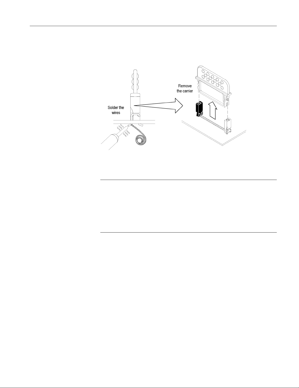
Replace the retention post wires
Perform the following procedure to replace the shorter retention post wires with
the longer wires:
1. Remove the old wire by pulling the side of the wire over the retaining tab and
lifting the wire away from the post.
2. Place the new wire in the slot side without the tab, and then wrap the wire over
the tab side until it engages in the slot (you will feel or hear a slight click).
Appendix A: Probe retention assembly installation information
Figure 26: Replacing the wires on the retention posts
Install the retention posts on the PCB
To install the retention posts on the PCB, do the following:
1. On the retention post/carrier assembly, locate the black retention post (the
post with the keying pin) and align it to the keying pin hole on the PCB.
eFigure27.)
(Se
2. Press the retention posts into the holes on the footprint on the PCB.
TE. The following two steps – bending and soldering the wires to the circuit
NO
board – are the two most important steps in assuring that the probe retaining
posts are correctly mounted. Bending the wires before soldering them helps
prevent long-term cold solder flow.
P5960 Logic Analyzer Probe Instruction Manual 39
Page 54

Appendix A: Probe retention assembly installation information
3. Press down on th
the PCB. Ensure the assembly is perpendicular to the PCB when bending
and soldering the post wires.
The bend point in the retaining wire should be as close to the circuit board
surface as possible. Grip the wire with a pair of needle-nose pliers about
1/8-inch above the circuit board surface and let the side of the through-hole
(not the pliers) act as the fulcrum point for bending the wire. This method
pulls the probe mounting posts tightly against the circuit board surface.
e carrier and bend the post wires out to anchor the posts to
Figure 27: Installing the retention posts on the PCB
40 P5960 Logic Analyzer Probe Instruction Manual
Page 55
Appendix A: Probe retention assembly installation information
4. Solder the post
the top or bottom of the circuit board, but it is best to solder the bottom to
avoid the heat-sinking effects of the posts on top.
Figure 2
5. Pull off
NOTE. The posts may have a small amount of movement after you solder them to
the circuit board. This is normal and accounted for in the post design.
8: Soldering the retention posts on the PCB
s to the PCB. (See Figure 28.) The posts can b e soldered from
the carrier from the posts.
The probe should mate firmly to the board when the two screws are tightened to
the mounting posts. The screws have a mechanical stop on them to prevent overtightening the probe to the board.
After a probe has been installed and removed, there may be slightly more play in
the posts. This is also normal and accounted for in the probe design.
P5960 Logic Analyzer Probe Instruction Manual 41
Page 56

Appendix A: Probe retention assembly installation information
42 P5960 Logic Analyzer Probe Instruction Manual
Page 57

Glossary
cLGA
An acronym for compression Land Grid Array, a connector that provides an
electrical connection between a PCB and the probe input circuitry.
Compression footprint
A connecto
Connection is obtained by applying pressure between your PCB and the probe
through a cLGA c-spring.
D-Max probing technology
The name that describes the technology used in the P5960 high-density logic
analyzer probe.
Functional check procedure
Functional check procedures verify the basic functionality of the p robes by
confirming that the probes recognize signal activity at the probe tips.
Keep out area
An area on a printed circuit board in which component, trace, and/or via
placement may be restricted.
Logic analyzer-end
The end of the probe which connects to the logic analyzer.
PCB
An acronym for Printed Circuit Board.
rless, solderless contact between your PCB and the P5960 probes.
robe head
P
The end of the probe that connects to the SUT.
SUT
System-Under-Test. Also known as the target system. The logic analyzer
connects to the SUT through the probe.
P5960 Logic Analyzer Probe Instruction Manual 43
Page 58

Glossary
44 P5960 Logic Analyzer Probe Instruction Manual
Page 59

Index
Symbols and Numbers
3D CAD file, 19, 24
A
accessories, 2
attaching labels, 5
C
calibration, 31
channel mapping, 27
channel
cleaning, 32
cLGA interface clip, 7
cLGA Interface Clip
clock channels, 15
clock
compression footprints
connecting
width, 15
replacing, 32
s, 15
cleaning, 37
probes to logic analyzer, 9
probes to the SUT, 9
D
multiplex data, 16
de
destination channels, 16
dimensions
probe, 18
retention assembly, 18
retention assembly
footprint, 20
retention assembly
side-by-side layout, 20
retention post footprint, 22
retention post side-by-side
layout, 22
retention posts, 20
double probing signals, 15
E
electrical considerations, 23
electrical model, 24
electrical specifications, 29
environmental specifications, 29
F
file attachments, 19, 24
footprint
footprints
functional check, 31
, 18, 27
dimensions, 24
retention assembly
dimensions, 20
retention assembly layout, 20
retention post dimensions, 22
on post layout, 22
retenti
cleaning, 37
H
handling the probe head, 7
hardware order, 17
I
pection and cleaning, 32
ins
installing retention posts, 39
interface clip
protecting, 12
K
keep out area
retention assembly, 19
keepout area
retention posts, 21
keying pin, 37
L
label
installation, 5
labels, 3
load model, 24
logic analyzer
connecting probes, 9
M
MagniVu memory, 17
main me mory
extra timing, 17
maintenance
functional check, 31
inspection and cleaning, 32
probe calibration, 31
probe rep
service strategy, 31
mechanical considerations, 23
mechanical specifications, 29
multiplexed buses, 16
ackaging, 33
O
ordering parts, 35
P
signments, 27
pad as
pad finishes, 24
PCB board area, 25
probe
cable managers, 11
connecting probes to the
,9
SUT
connection problems, 12
cover, 12
description, 1
dimensions, 18
dress the probe cables, 11
footprint dimensions, 24
labels, 3
repackaging, 33
storing the probe head, 12
troubleshooting, 12
probe connections
to the instrument, 9
to the logic analyzer, 9
probe head
handling, 7
protective cover, 8
P5960 Logic Analyzer Probe Instruction Manual 45
Page 60

Index
Q
qualifier channels, 15
R
range recog
related documentation, ix
repackage the probe, 33
replacement parts, 35
replacing the cLGA interface
clip, 32
retentio
dimensions, 18
footprint dimensions, 20
footprint layout, 20
installing, 37
nizers, 17
n assembly, 24
retention post
dimensions, 20
footprint dimensions, 22
footprint layout, 22
installing, 39
keepout area, 21
wires, 39
s, 38
S
Safety Summary, v
service options, 31
signal names, 27
signal routing, 23
solder mask, 25
source c
hannels, 16
demultiplexing, 17
specifications
electrical, 29
environmental, 29
mechanical, 29
SUT
connecting probes, 9
T
timing ana
transmission lines, 23
troubleshooting
lysis, 15
probe connections, 12
V
via-in-pad, 25
vias, 25
Vias, 2
1
46 P5960 Logic Analyzer Probe Instruction Manual
 Loading...