

Page 1

xx
P5934
ZZZ
Mass Termination Probe
Instruction Manual
www.tektronix.com
P077063600*
*
077-0636-00
Page 2

Copyright © Tektronix. All rights reserved. Licensed software products are owned by Tektronix or its subsidiaries
or suppliers, and are protected by national copyright laws and international treaty provisions.
Tektronix products are covered by U.S. and foreign patents, issued and pending. Information in this publication
supersedes that in all previously published material. Specifications and price change privileges reserved.
TEKTRONIX and TEK are registered trademarks of Tektronix, Inc.
MagniVu is a trademark of Tektronix, Inc.
Contacting Tektronix
Tektronix, Inc.
14150 SW Karl Braun Drive
P.O. Box 500
Beaverton, OR 97077
USA
For product information, sales, service, and technical support:
In North America, call 1-800-833-9200.
Worl dwid e, v isit www.tektronix.com to find contacts in your area.
Page 3

Warranty
Tektronix warrants that this product will be free from defects in materials and workmanship for a period of one (1)
year from the date of shipment. If any such product proves defective during this warranty period, Tektronix, at its
option, either will repair the defective product without charge for parts and labor, or will provide a replacement
in exchange for the defective product. Parts, modules and replacement products used by Tektronix for warranty
work may be n
the property of Tektronix.
ew or reconditioned to like new performance. All replaced parts, modules and products become
In order to o
the warranty period and make suitable arrangements for the performance of service. Customer shall be responsible
for packaging and shipping the defective product to the service center designated by Tektronix, with shipping
charges prepaid. Tektronix shall pay for the return of the product to Customer if the shipment is to a location within
the country in which the Tektronix service center is located. Customer shall be responsible for paying all shipping
charges, duties, taxes, and any other charges for products returned to any other locations.
This warranty shall not apply to any defect, failure or damage caused by improper use or improper or inadequate
maintenance and care. Tektronix shall not be obligated to furnish service under this warranty a) to repair damage
result
b) to repair damage resulting from improper use or connection to incompatible equipment; c) to repair any damage
or malfunction caused by the use of non-Tektronix supplies; or d) to service a product that has been modified or
integrated with other products when the effect of such modification or integration increases the time or difficulty
of servicing the product.
THIS WARRANTY IS GIVEN BY TEKTRONIX WITH RESPECT TO THE PRODUCT IN LIEU OF ANY
OTHER WARRANTIES, EXPRESS OR IMPLIED. TEKTRONIX AND ITS VENDORS DISCLAIM ANY
IMPLIED WARRANTIES OF MERCHANTABILITY OR FITNESS FOR A PARTICULAR PURPOSE.
TRONIX' RESPONSIBILITY TO REPAIR OR REPLACE DEFECTIVE PRODUCTS IS THE SOLE
TEK
AND EXCLUSIVE REMEDY PROVIDED TO THE C USTOMER FOR BREACH OF THIS WARRANTY.
TEKTRONIX AND ITS VENDORS WILL NOT BE LIABLE FOR ANY INDIRECT, SPECIAL, INCIDENTAL,
OR CONSEQUENTIAL DAMAGES IRRESPECTIVE OF WHETHER TEKTRONIX OR THE VENDOR HAS
ADVANCE NOTICE OF THE POSSIBILITY OF SUCH DAMAGES.
[W2 – 15AUG04]
btain service under this warranty, Customer must notify Tektronix of the defect before the expiration of
ing from attempts by personnel other than Tektronix representatives to install, repair or service the product;
Page 4

Page 5

Table of Contents
General safety summary ........ .................................. ................................ ................ iv
Environmental considerations............................................ .................................. ...... vi
Preface ............................................................................................................. vii
Related doc
Operating basics ..... .................................. ................................ ............................. 1
Product description ........... ................................ ................................ ................. 1
Probe accessory information ................................................................................. 2
Probe label overview ..................... ................................ .................................. ... 3
Apply the labels to the probe.. ................................ ................................ ............... 4
Connect
SUT probe connection overview............................................................................. 9
Connect the probe directly to the SUT ..................................................................... 10
Connect the probes using the Mictor adapter .............................................................. 12
Disconnect the probe from the SUT.. ................................ ................................ ...... 14
Reference......... ................................ .................................. ................................ 15
or connectors and latch housings ...................................................................... 15
Mict
P5934 probe dimensions ........................... ................................ .......................... 17
Dimensions and placement of Mictor connectors ......................................................... 18
Mechanical layout and pin numbering sequence .......................................................... 19
Standard probe channel assignments ....................................................................... 21
Alternate probe channel assignments....................................................................... 23
ading and equivalent circuits ............................................................................. 25
Lo
Specifications...... .................................. ................................ .......................... 26
Maintenance........................................................................................................ 29
Probe calibration information ... ................................ ................................ ............ 29
Probe service strategy information.......................................................................... 29
Inspect or clean the probe............................................ ................................ ........ 29
Perform the functional check .......................... .................................. .................... 30
Repackage the probe ......................................................................................... 30
Replaceable Parts .................................................................................................. 31
Parts ordering information ................................................................................... 31
Glossary
Index
umentation............... ................................ ................................ ....... vii
the probe to the logic analyzer.......... .................................. ......................... 9
P5934 Logic Analyzer Probe Instruction Manual i
Page 6

Table of Contents
List of Figure
Figure 1: P5934 Mass Termination Probe .. ................................ .................................. ... 1
Figure 2: P5
Figure 3: Locating the probe-tip connector...................................................................... 5
Figure 4: End view of the probe-tip connector............. ................................ ..................... 5
Figure 5: Other indicators for pin 1 side .......................... ................................ ............... 6
Figure 6: Location of the pin 38 side label on the probe-tip........ .................................. ......... 6
Figure 7: Applying labels to the probe connectors ...... ................................ ....................... 7
Figure 8:
Figure 9: Connecting the logic analyzer probe............................. ................................ ..... 9
Figure 10: Connecting to a surface- or edge-mounted connector ............................................ 11
Figure 11: Mictor adapters . ................................ ................................ ...................... 12
Figure 12: Dimensions of the Mictor adapters ............. ................................ .................... 12
Figure 13: Clearance for probe connection using the Mictor adapter ....................................... 13
e 14: Releasing the probe tip from the latch housing ................................................... 14
Figur
Figure 15: Latch housing dimensions ........................................................................... 16
Figure 16: P5934 probe dimensions..................... ................................ ........................ 17
Figure 17: Vertical dimensions of the probe.................................. ................................ .. 18
Figure 18: Dimensions and placement of a surface-mounted Mictor connector with latch housing . .... 18
Figure 19: Surface-mounted connector layout (component side) ............................................ 19
gure 20: Edge-mounted connector layout (component side) ............................... ................ 20
Fi
Figure 21: Equivalent circuit for the probe..................................................................... 25
934 probe labels...................................................................................... 3
Probe label placement summary ...................................................................... 8
s
ii P5934 Logic Analyzer Probe Instruction Manual
Page 7

List of Tables
Table 1: Color-coded label combinations (136- and 102-channel logic analyzers) ......................... 3
Table 2: Col
Table 3: Compatible Mictor connectors........................................... .............................. 15
Table 4: Pin assignments () for Mictor connector (component side) ...................... .................. 21
Table 5: Pin 1 side probe channel assignments ................ .................................. .............. 22
Table 6: Pin 38 side probe channel assignments ............................................................... 22
Table 7: Nonstandard pin assignment for Mictor connector (component side)............................. 23
Table 8 : P
Table 9: Pin 38 side probe channel assignments (nonstandard) .............................................. 24
Table 10: Lossy delay line values ............... .................................. .............................. 26
Table 11: Electrical and mechanical specifications .................... ................................ ........ 26
Table 12: Environmental specifications......................................................................... 27
Table 13: Service options......................................................................................... 29
or-coded label combinations (68- and 34-channel logic analyzers) ............................ 4
in 1 side probe channel assignments (nonstandard) ................. .............................. 24
Table of Contents
P5934 Logic Analyzer Probe Instruction Manual iii
Page 8

General safety summary
General safet
To avoid fire or personal
injury
ysummary
Review the fo
this product or any products connected to it.
To avoid pot
Only qualified personnel should perform service procedures.
While using this product, you may need to access other parts of a larger system.
Read the safety sections of the other component manuals for warnings and
cautions r
Connect and disconnect properly. Do not connect or disconnect probes or test
leads while they are connected to a voltage source.
Observe all terminal ratings. To a voi d fire or shock hazard, observe all ratings
and markings on the product. Consult the product manual for further ratings
information before making connections to the product.
Do not apply a potential to any terminal, including the common terminal, that
exceeds the maximum rating of that terminal.
Do not operate without covers. Do not operate this product with covers or panels
removed.
llowing safety precautions to avoid injury a nd prevent damage to
ential hazards, use this product only as specified.
elated to operating the system.
Do not operate with suspected failures. If you suspect that there is damage to this
product, have it inspected by qualified service personnel.
Avoid exposed circuitry. Do not touch exposed connections and components when
power is present.
Use proper AC adapter. Use only the AC adapter specified for this p roduct.
Use proper fuse. Use only the fuse type and rating specified for this product.
Do not operate in wet/damp conditions.
Do not operate in an explosive atmosphere.
Keep product surfaces clean and dry.
Provide proper ventilation. Refer to the manual's installation instructions for details
on installing the product so it has proper ventilation.
iv P5934 Logic Analyzer Probe Instruction Manual
Page 9
General safety summary
Terms in this manual
Symbols and terms on the
product
These terms may
WAR NI NG . Warning statements identify conditions or practices that could result
in injury or loss of life.
CAUTION. Caution statements identify conditions or practices that could result in
damage to this product or other property.
These terms may appear on the product:
DANGER in
the marking.
WARNING
read the marking.
CAUTIO
The following symbol(s) may appear on the product:
appear in this manual:
dicates an injury hazard immediately accessible as you rea d
indicates an injury hazard not immediately accessible as you
N indicates a hazard to property including the product.
P5934 Logic Analyzer Probe Instruction Manual v
Page 10
Environmental considerations
Environmental considerations
This section lists the environmental standards with which the instrument complies.
Product end-of-life
handling
Restriction of hazardous
substances
Observe the following guidelines when recycling an instrument or component:
Equipment recycling. Production of this equipment required the extraction and
use of natural resources. The equipment may contain substances that could be
harmful to
end of life. To avoid release of such substances into the environment and to
reduce the use of natural resources, we encourage you to recycle this product in
an appropriate system that will ensure that most of the materials are reused or
recycled appropriately.
This product is classified as an industrial monitoring and control instrument
accessory, and is not required to comply with the substance restrictions of the
recast RoHS Directive 2011/65/EU until July 22, 2017.
the environment or human health if improperly handled at the product’s
This sym
Union requirements according to Directives 2002/96/EC and 2006/66/EC
on waste electrical and electronic equipment (WEEE) and batteries. For
informa
Tektronix Web site (www.tektronix.com).
bol indicates that this product complies with the applicable European
tion about recycling options, check the Support/Service section of the
vi P5934 Logic Analyzer Probe Instruction Manual
Page 11

Preface
Preface
Related documentation
This documen
The followi
t provides information on using the P5934 logic analyzer probe.
ng list and table provide information on the related documentation
available for your Tektronix product. For additional information, refer to the
Tektronix Web site (www.tektronix.com/manuals).
Related documentation
Item Purpose
TLA Quick Start User Manuals
Online Help
Installation Reference Sheets High-level installation information
Installation Manuals
XYZs of Logic Analyzers
Declassification and Securities instructions Data security concerns speci fic to sanitizing
Application notes
Product Specifications & Performance
Verification Procedures
Field upgrade kits
Optional Service Manuals Self-service documentation for modules and
High-level operational overview
In-depth operation and UI help
Detailed first-time installation information
Logic analyzer basics
or removing memory devices from Tektronix
products
Collection of logic analyzer application
specific notes
TLA Product specifications and performance
verification procedures
Upgrade information for your logic analyzer
mainframes
P5934 Logic Analyzer Probe Instruction Manual vii
Page 12

Preface
viii P5934 Logic Analyzer Probe Instruction Manual
Page 13
Operating basics
Product description
This section provides a brief description of the Tektronix P5934 Mass Termination
Logic Analyzer Probe, information on attaching color-coded probe labels, and
instruction
the SUT (system-under-test).
The P5934 probe connects 34 logic analyzer channels directly to the SUT or to a
microprocessor probe adapter on the SUT.
The probe acquires data from 32 input or output signals and two clocks, one clock
and one qualifier, or two qualifier signals.
s for connecting the probe and adapters from the logic analyzer to
Figure 1: P 5934 Mass Termination Probe
The following list describes the capabilities and qualities o f the P5934 probe:
Single-ended data and single-ended clock inputs
Consists of one independent probe tip of 34 channels (32 data and 2
clock/qualifiers), and two 17-channel probe connectors
Provides a means of connecting multiple channels to be quickly connected to
a small footprint on the SUT
P5934 Logic Analyzer Probe Instruction Manual 1
Page 14
Operating basics
Probe accesso
ry information
The P5934 probe includes accessories to connect the logic analyzer to the SUT.
The following accessories are available :
Latch housing assembly, edge-mount
Latch housing assembly, vertical
Mictor con
Mictor connector kit (Tektronix part number, 020-2228-xx; kit of 21 surface
mount ver
Probe labels
P5934 Logic Analyzer Probe Instructions (Tektronix part number,
071-2976-xx)
P5934 High-Density Logic Analyzer Probe Instruction Manual (Tektronix
part number, 077-0636-xx, available on the TLA Documentation CD or
downlo
The following optional accessories are available for the probe:
17-Channel Compression-on-PCB to Mictor adapter (Tektronix part number,
020-2455-xx)
nector (surface mount, vertical receptacle)
tical receptacle connectors)
adable from the Tektronix Web site: w ww.tektronix.com/manuals)
34-Channel Compression-on-PCB to Mictor adapter (Tektronix part number,
020-2456-xx)
2 P5934 Logic Analyzer Probe Instruction Manual
Page 15

Probe label overview
Operating basics
The probe comes with color-coded labels to apply to the probe before connecting
the probe to the logic analyzer and to the SUT.
Figure 2: P5934 probe labels
The labeling scheme for th
packages and on the SUT for signal and channel assignments.
NOTE. Use one Pin 1 label for each probe connector. Do not use two labels with
a pin 1 indicator or two labels without a pin 1 indicator on a single probe.
The following tables describe the color-coded label combinations for 136- and
102-channel logic analyzers and for 68- and 34-channel logic analyzers. Use the
extra labels, as needed, from the label sheet.
Table 1: Color-coded label combinations (136- and 102-channel logic analyzers)
Address
Color on Pin 1 side Tan (CK:0, A3:7-0, A2:7-0)
Color on Pin 38 side Orange (CK:1, A1:7-0, A0:7-0)
e probe occurs on most microprocessor support
P5934 Logic Analyzer Probe Instruction Manual 3
Page 16

Operating basics
Table 1: Color-coded label combinations (136- and 102-channel logic analyzers)
(cont.)
Address
Data
Color on Pin 1 side Blue (QUAL:0, D3:7-0, D2:7-0)
Color o n Pin 38 side Yellow (CK:2, D1:7-0, D0:7-0)
Control
Color on Pin 1 side White (CK:3, C3:7-0, C2:7-0)
Color on Pin 38 side Gray (QUAL:1, C1:7-0, C0:7-0)
Extended (136 instruments only)
Color on Pin 1 side Green (QUAL:3, E3:7-0, E2:7-0)
Color on Pin 38 side Violet (QUAL:2, E1:7-0, E0:7-0)
Table 2: Color-coded label combinations (68- and 34-channel logic analyzers)
ColoronPin1side(Control)
Color on Pin 38 side (Address) Blank (write in, CK:0, A3:7-0, A2:7-0)
For a 68 channel instrument
Color on Pin 1 side (Address) Tan (CK:0, A3:7-0, A2:7-0)
Color on Pin 38 side (Address) Orange (CK:1, A1:7-0, A0:7-0)
ColoronPin1side(Control) White(CK:3,C3:7-0,C2:7-0)
Color on Pin 38 side (Data) Yellow (CK:2, D1:7-0, D0:7-0)
Apply the labels to the probe
Attach the labels to the probe connector and to both sides of the probe tip.
NOTE. Use flat-nosed tweezers to remove the labels from the sheet of labels.
Never peel labels with your fingers. The labels are made of soft vinyl and can
stretch and distort easily. To avoid stretching the label, always hold it from the top
right corner while removing it from the sheet of labels.
The adhesive on the vinyl labels is extremely strong. Carefully align each label to
the intended outline on the probe connector and probe tip before attaching it to the
probe. Once labels are placed on the probe, they become very difficult to remove.
White
(CK:3, C3:7-0, C2:7-0)
4 P5934 Logic Analyzer Probe Instruction Manual
Page 17

Operating basics
To apply labels
1. Locate the labels that you need for the probe from the provided label sheets,
but do not peel
If you need help determining which labels to use, see the following steps:
a. Determine which channel group on the logic analyzer that you want to
connect the probe; note the color-coded labels on the logic analyzer.
b. Look at the label sheets and locate the labels that match the logic analyzer
channel group that you need to use. Notice that there are two different
sizes of la
2. Locate the probe-tip connector on the probe.
to the probe, complete the following steps:
them off yet.
bels for each channel group:
Probe-tip labels (smaller)
Probe connector labels (larger)
Blank labels (custom channel combinations not recommended)
Figure 3: Locating the probe-tip connector
3. Locate the pin 1 side of the probe-tip connector by using the end view of the
be-tip connector.
pro
The position of the bent waves, the angled ends, are on the pin 1 side.
Figure 4: End view of the probe-tip connector
4. Remove the pin 1 side label that you need from the sheet of labels.
P5934 Logic Analyzer Probe Instruction Manual 5
Page 18

Operating basics
5. Applythepin1s
NOTE. You can also use the small pin 1 recess or the beveled corners on the probe
tip end of the connector, but both are difficult to find. (See Figure 5 on page 6.)
Figure 5: Other indicators for pin 1 side
6. Apply the associated pin 38 side label to the probe tip. (See Figure 6.)
If necessary, see the color-coded combination tables on the previous pages
for label information.
ide label to the pin 1 side of the probe-tip connector.
Figure 6: Location of the pin 38 side label on the probe-tip
6 P5934 Logic Analyzer Probe Instruction Manual
Page 19

Operating basics
7. Apply the probe
page 7.)
To avoid misla
to the probe connector. Match the color of the probe connector label to the
probe-tip label.
connector labels to the probe connectors. (See Figure 7 on
belling, hold the probe-tip in your hand and follow the cable
Figure 7: Applying labels to the probe connectors
P5934 Logic Analyzer Probe Instruction Manual 7
Page 20

Operating basics
The following fi
gure summarizes the label placement for the probe.
Figure 8: Probe label placement summary
8 P5934 Logic Analyzer Probe Instruction Manual
Page 21

Operating basics
Connect the pr
obe to the logic analyzer
The probe connects a TLA6400 Series logic analyzer to the SUT. You can connect
the probe to the SUT without turning off the power to the SUT.
Appy the labels to the probes before connecting the probes to the logic analyzer
andtotheSUT.
1. Match the color-coded labels of the probe to the same color-coded connector
on the logic analyzer.
2. Connect the logic analyzer probe as shown.
Figure 9: Connecting the logic analyzer probe
SUT probe connection overview
probe connects to surface-mounted or edge-mounted Mictor connectors on
The
the SUT.
termine how you intend to connect the probes to the SUT. Then install the
De
Mictor connectors on the SUT before connecting the probes.
e one of the following methods to connect the probe to the SUT:
Us
Connect to the SUT directly to a Mictor connector on the SUT.
Connect to the SUT through a Mictor adapter.
In the following procedures, a surface-mounted Mictor connector is shown in the
illustrations. The procedures are the same for the edge-mounted connector.
P5934 Logic Analyzer Probe Instruction Manual 9
Page 22

Operating basics
Connect the pr
obedirectlytotheSUT
Connect to the SUT directly to a Mictor connector (either surface-mounted or
edge-mounted connector) on the SUT.
To connect the probe directly to a Mictor connector on the SUT, complete the
following steps:
1. Line up the pin 1 indicator on the probe tip with pin 1 on the connector on
the PCB on the SUT. The Mictor connector is keyed to prevent incorrect
connectio
CAUTION. To avoid damaging the probe and SUT, always position the probe
perpendicular to the mating connector and gently connect the probe. Incorrect
handling of the probe while connecting it to the SUT can result in damage to the
probe or to the mating connector on the SUT.
NOTE. If you have custom channel combinations for the mictor connector on your
SUT, use the blank sheet of labels to create your own pin 1 and pin 38 side labels.
Use one Pin 1 label for each probe connector. Do not use two labels with a pin
1 indicator or two labels without a pin 1 indicator on a single probe.
Custom labeling is an option, though not recommended.
ns.
2. Position the probe tip perpendicular to the connector, and gently connect the
probe as shown in the following fi gure. (See Figure 10 on page 11.)
3. When connected, push the latch releases on the probe to set the latch.
10 P5934 Logic Analyzer Probe Instruction Manual
Page 23

Operating basics
Figure 10: Connecting to a surface- or edge-mounted connector
P5934 Logic Analyzer Probe Instruction Manual 11
Page 24

Operating basics
Connect the pr
obes using the M ictor adapter
The Compression-on-PCB to Mictor adapters provide a means of connecting
the probe to take advantage of the new compression footprint and eliminate the
need for Mict
Two different adapters are available:
17-Channel Mictor adapter
34-Channel Mictor adapter
or connectors in your SUT.
Figure 11: Mictor adapters
Two different screw lengths are required to accommodate the 0.050-inch -
0-inch (1.27 mm - 6.35 mm) PCB thickness range.
0.25
This adapters require the use of the Compression-on-PCB to Mictor adapter land
print. The following figure provides dimensional information; the dimensions
foot
are the same for both adapters.
Figure 12: Dimensions of the Mictor adapters
12 P5934 Logic Analyzer Probe Instruction Manual
Page 25

Operating basics
Compare the cle
Mictor adapter. (See Figure 13.) Note that the difference in clearance between
the probe connection and the connection using the Mictor adapter is 3.68 mm
(0.145-in.).
arance between the p robe connection and the connection via the
Figure 13: Clearance for probe connection using the Mictor adapter
P5934 Logic Analyzer Probe Instruction Manual 13
Page 26

Operating basics
Disconnect th
e probe from the SUT
To disconnect the probe, complete the following steps:
1. Gently pull the latch release grip to release the probe tip from the latch
housing as shown in the following figure. (See Figure 14.)
Figure 14: Releasing the probe tip from the latch housing
CAUTION. To avoid damage to the probe and mating connector, hold on to the
release grip and gently pull the probe straight out of the connector. Do not
latch
tilt the p robe in any direction when disconnecting it. Tilting the probe can damage
the probe and mating connector.
2. Continue to pull the probe tip straight out of the mating connector using the
latch release grip.
If you use an extender, grip the corners of the circuit board-end attached to the
SUT, and gently pull it straight out of the connector.
14 P5934 Logic Analyzer Probe Instruction Manual
Page 27

Reference
This section provides guidelines for designing a P5934 probe interface on the SUT.
Mictor conne
ctors and latch housings
The probe contains 34 sets of signal connections (32 data channels and two clock
or qualifier channels).
The probe tip connection is a 38-pin Mictor connector. The following table lists
Mictor connectors you can purchase that are compatible with the probe and
compatib
Table 3: Compatible Mictor connectors
Tektronix part number Description
131-6134-01 Probe,tip; terminal ,calibrator 0.250 Hex
131-6520-00
105-1088-xx
105-1089-xx
Latch housing mechanisms to use with the Mictor connectors are available for
purchase. The latch housing surrounds the Mictor connector on your SUT and
provides positive retention of the probe.
le latch housings and connectors.
C36000 gold plated, calgrator terminal
Connector receptical; edge mount, Mictor;
female, right-angle, 38 POS, 0.025 center,
PD NI matched impedance
Latch housing; edge mount (0.062 inch
circuit board thickness)
Latch housing; surface mount
The following figure shows the dimensions of the optional latch housings.
P5934 Logic Analyzer Probe Instruction Manual 15
Page 28

Reference
Figure 15: Latch housing dimensions
16 P5934 Logic Analyzer Probe Instruction Manual
Page 29

P5934 probe dimensions
The following figure shows the dimensions of the P5934 probe,
Reference
Figure 16: P5934 probe dimensions
P5934 Logic Analyzer Probe Instruction Manual 17
Page 30

Reference
Dimensions an
d placement of Mictor connectors
Use compatible surface-mounted or edge-mounted Mictor connectors in your
circuit board design. Place the connector as close as possible to the device under
test.
The following figure shows the vertical dimensions of the probe.
Figure 17: Vertical dimensions of the probe
The following figure shows the dimensions and minimum placement of
surface-mounted connectors on a SUT. The side-to-side dimension between
connectors also applies to the edge-mounted connector.
Figure 18: Dimensions and placement of a surface-mounted Mictor connector with
tch housing
la
18 P5934 Logic Analyzer Probe Instruction Manual
Page 31
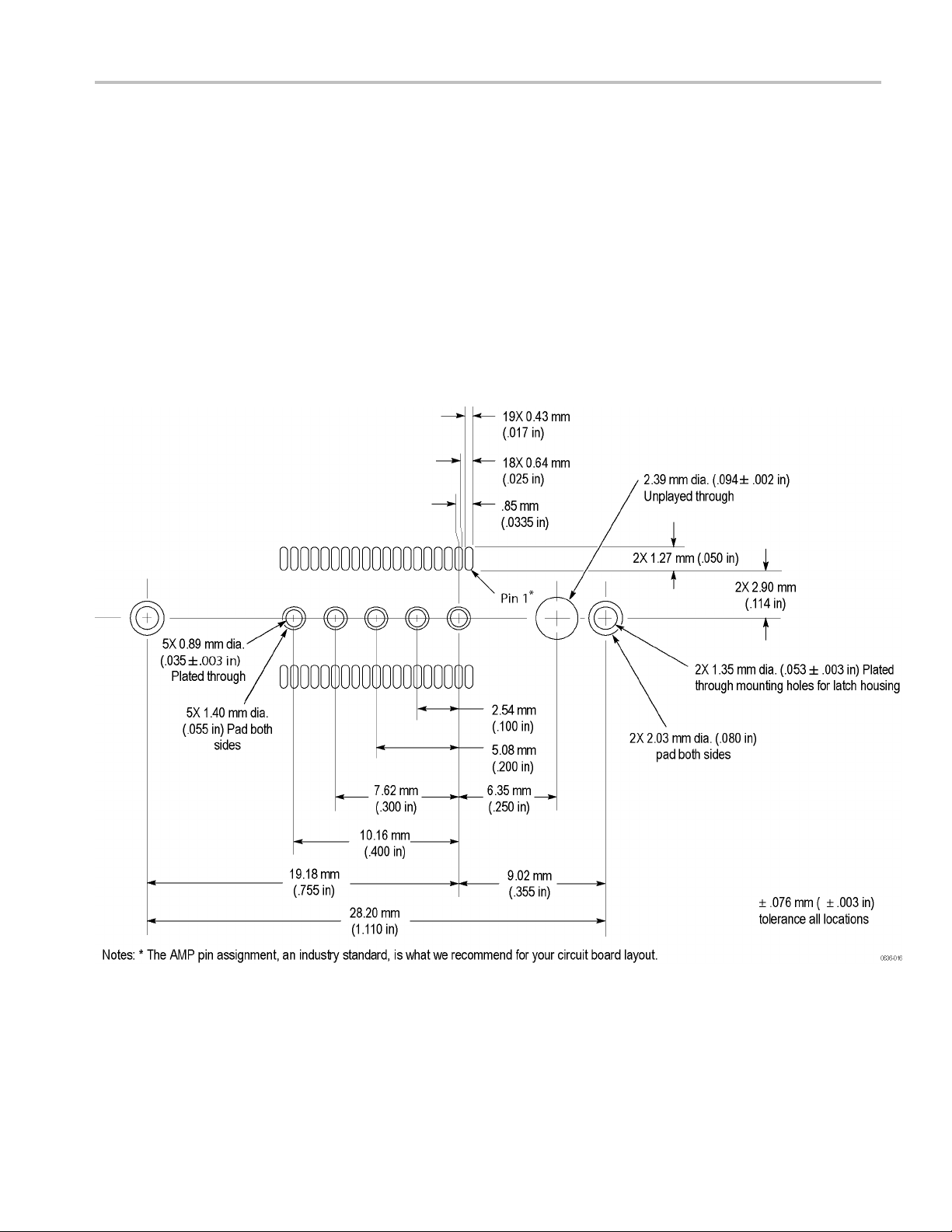
Mechanical layout and pin numbering sequence
Use the correct mechanical layout and pin numbering sequence for your design.
Compatible Mictor connectors have 43 pins; pins 39 through 43 are grounded.
Pins 1, 2, 37, and 38 are open. The following figure shows the positions and
spacing between the pins, the keyhole, and the latch housing mounting holes
of a surface-mounted connector. Refer to the pin assignment table for the
recommended pin assignments. (See Table 4 on page 21.)
If you include the latch housing in your design, place a pin 1 indicator on your
circuit board during design because the latch housing obscures the pin 1 indicator
on the Mic
need to know the location of pin 1 when connecting the probe.
tor connector. Even though the Mictor connector is keyed, you still
Reference
Figure 19: Surface-mounted connector layout (component side)
P5934 Logic Analyzer Probe Instruction Manual 19
Page 32

Reference
The following fi
housing mounting holes of a edge-mounted connector.
NOTE. The edge-mounted connector does not have a keyhole. Be sure to position
pin 1 correctly when building the SUT to maintain the correct mapping of signals
from your SUT to the logic analyzer probe sections and channels.
gure shows the positions and spacing between the pins and latch
re 20: Edge-mounted connector layout (component side)
Figu
20 P5934 Logic Analyzer Probe Instruction Manual
Page 33

Reference
Standard prob
e channel assignments
Tektronix recommends using the standard Probe channel assignments for your
design.
The 17 channels to which the probe connects on the logic analyzer cannot be
changed. When mapping signals from your SUT to channels on the logic analyzer,
keep the pro
tables. (See Table 1 on page 3.) (See Table 2 on page 4.)
Each probe
Pins 1, 2, 3, and 4 are unused.
The prefe
CAD packages use the numbering scheme as the industry standard. (See Table 4
on page 21.) The table shows the pin assignments for the surface-mounted
connector. Pin assignments are the same for the edge-mounted connector.
The standard probe channel assignment uses an odd-side even-side pin
assignment. Pin 1 is located at the top left, and pin 3 is located directly below it.
Pin 2 is located on the top right, and pin 4 is located directly below it. Refer to the
table for the pin assignments. (See Table 5.)
NOTE
pin-numbering sequence your CAD system uses.
be section, clock, and/or qualifier channels together as shown in the
connector has 43 pins; pins 39 through 43 are the five ground pins.
rred pin assignment is the pin assignment because other commercial
. When designing Mictor connectors into your SUT, always verify which
le 4: Pin assignments () for Mictor connector (component side)
Tab
Type of pin assignment Comments
Preferred. This pin assignment is the
industry standard and is what Tektronix
commends that you use.
re
The following tables show the sections and channels and the probe pins to
which they connect. (See Table 5.) (See Table 6 on page 22.) The tables also
comply with the labeling schemes in the previous tables except for the 34-channel
instrument on the Pin 38 side of the p robe. The Mictor pin numbers are shown
for reference only.
P5934 Logic Analyzer Probe Instruction Manual 21
Page 34

Reference
NOTE. The label
ing scheme for a 34 or 68 channel instrument is listed in a
previous table. (See Table 2 on page 4.)
Table 5: Pin 1
pin number A probe C probe D probe E probe
5
7
9 A3:6
11 A3:5
13 A3:4
15 A3:3
17 A3:2
19 A3:1
21 A3:0
23 A2:7
25 A2:6
27 A2:
29 A2:
31 A2
33 A2
5
3
37 A2:0
side probe channel assignments
Section and channel
CLK:0 CLK:3 Q0 Q3
A3:7
2:1
A
C3:7
C3:6
C3:5
C3:4
C3:3
C3:2
C3:1
C3:0
C2:7
C2:6
5
4
:3
:2
C2:5
C2:4
C2:3
C2:2
C2:1
C2:0
D3:7 E3:7
D3:6 E3:6
D3:5 E3:5
D3:4 E3:4
D3:3 E3:3
D3:2 E3:2
D3:1 E3:1
D3:0 E3:0
D2:7 E2:7
D2:6 E2:6
5
D2:
4
D2:
:3
D2
:2
D2
2:1
D
D2:0 E2:0
E2:
E2:
E2
E2
E
5
4
:3
:2
2:1
Table 6: Pin 38 side probe channel assignments
Section and channel
pin number A probe C probe D probe E probe
6
8 A1:7
10 A1:6
12 A1:5
14 A1:4
16 A1:3
18 A1:2
20 A1:1
22 A1:0
24 A0:7
26 A0:6
CLK:1 Q1 CLK:2 Q2
C1:7
C1:6
C1:5
C1:4
C1:3
C1:2
C1:1
C1:0
C0:7
C0:6
D1:7 E1:7
D1:6 E1:6
D1:5 E1:5
D1:4 E1:4
D1:3 E1:3
D1:2 E1:2
D1:1 E1:1
D1:0 E1:0
D0:7 E0:7
D0:6 E0:6
22 P5934 Logic Analyzer Probe Instruction Manual
Page 35

Table 6: Pin 38 side probe channel assignments (cont.)
Section and channel
pin number A probe C probe D probe E probe
28 A0:5
30 A0:4
32 A0:3
34 A0:2
36 A0:1
38 A0:0
Alternate p robe channel assignments
An alternate probe channel assignment is available. However, it is not
recommended due to incompatibility with commercial CAD packages.
The17channelstowhichtheendconnectsonthelogicanalyzercannotbe
changed. When mapping signals from your target system to channels on the
logic analyzer, you must keep the probe section, clock, and/or qualifier channels
together. Each probe connector has 43 pins; pins 39 through 43 are the five
ground pins. Pins 1, 2, 37, and 38 are unused, and it is recommended that they be
nnected to ground.
co
C0:5
C0:4
C0:3
C0:2
C0:1
C0:0
Reference
D0:5 E0:5
D0:4 E0:4
D0:3 E0:3
D0:2 E0:2
D0:1 E0:1
D0:0 E0:0
The pin assignment is counterclockwise with Pin 1 located at the top left, and pin
located directly below it. Pin 20 is located on the bottom right, and pin 21 is
2
located directly above it.
Table 7: Nonstandard pin assignment for Mictor connector (component side)
Type of pin assignment Comments
This pin assignment is no longer
recommended due to incompatibility with
other commercial CAD packages.
The following tables show the sections and channels and the probe pins to which
they connect. The tables comply with the labeling schemes in the previous tables
except for the 34-channel instrument on the Pin 38 side of the probe. The Mictor
pin numbers are shown for reference only.
P5934 Logic Analyzer Probe Instruction Manual 23
Page 36

Reference
Table8:Pin1si
Nonstandard
probe pin
number Aprobe Cprobe Dprobe Eprobe
3
4 A3:7
5
6 A3:5
7
8 A3:3
9 A3:2
10 A3:1
11 A3:0
12 A2:7
13 A2:6
14 A2:5
15 A2:4
16 A2:3
17 A2:2
18 A2:1
19 A2:0
de probe channel assignments (nonstandard)
Section and channel
CLK:0 CLK:3 Q0 Q3
D3:7 E3:7
D3:6 E3:6
D3:5 E3:5
D3:4 E3:4
D3:3 E3:3
D3:2 E3:2
D3:1 E3:1
D3:0 E3:0
D2:7 E2:7
D2:6 E2:6
D2:5 E2:5
D2:4 E2:4
D2:3 E2:3
D2:2 E2:2
D2:1 E2:1
D2:0 E2:0
A3:6
A3:4
C3:7
C3:6
C3:5
C3:4
C3:3
C3:2
C3:1
C3:0
C2:7
C2:6
C2:5
C2:4
C2:3
C2:2
C2:1
C2:0
Table 9: Pin 38 side probe channel assignments (nonstandard)
Nonstandard
probe pin
number A prob e C probe D probe E probe
36
35 A1:7
34 A1:6
33 A1:5
32 A1:4
31 A1:3
30 A1:2
29 A1:1
28 A1:0
27 A0:7
26 A0:6
25 A0:5
24 A0:4
23 A0:3
Section and channel
CLK:1 Q1 CLK:2 Q2
C1:7
C1:6
C1:5
C1:4
C1:3
C1:2
C1:1
C1:0
C0:7
C0:6
C0:5
C0:4
C0:3
D1:7 E1:7
D1:6 E1:6
D1:5 E1:5
D1:4 E1:4
D1:3 E1:3
D1:2 E1:2
D1:1 E1:1
D1:0 E1:0
D0:7 E0:7
D0:6 E0:6
D0:5 E0:5
D0:4 E0:4
D0:3 E0:3
24 P5934 Logic Analyzer Probe Instruction Manual
Page 37

Table 9: Pin 38 side probe channel assignments (nonstandard) (cont.)
Reference
Nonstandard
probe pin
number A prob e C probe D probe E probe
22 A0:2
21 A0:1
20 A0:0
Loading and equivalent circuits
Use the loading and equivalent circuits for the best design for your application.
Each signal line has a 20 kΩ ± 1% resistor (shunted by a 0.23 pF capacitor) in
series with an approximately five foot long section of 75 (Ω) coaxial cable. The
load presented to the SUT by the probe is low. The load is equivalent to a 2 pF
capacitance with 20 kΩ resistance returned to a 2.2 V supply. The following
ximation of the probe loading is sufficient for most circuit simulation
appro
calculations.
The following figure shows the equivalent circuit of the probe.
Section and channel
C0:2
C0:1
C0:0
D0:2 E0:2
D0:1 E0:1
D0:0 E0:0
Figure 21: Equivalent circuit for the probe
P5934 Logic Analyzer Probe Instruction Manual 25
Page 38

Reference
Specifications
The following t
able shows the values to calculate characteristics of the lossy
delay lines shown in the next two figures.
Table 10: Loss
Characteristic Value
C (capacitance)
L (inductance)
R (resistance) 0.067 Ω per inch
Z0(impedance) 75 Ω
y delay line values
1.58 pF per in
8.9 nH per in
ch
ch
.
The following tables list the electrical, mechanical, and environmental
specifications for the probe.
These specifications are for a P5934 probe c onnected between a logic analyzer
and a SUT. Refer to the TLA6400 Series Logic Analyzer Product Specifications
& Performance Verification Technical Reference Manual (available on the TLA
Docum
entation CD or downloadable from the Tektronix Web site) for a complete
list of system specifications. The probes are designed to meet Tektronix standard
062-2847-00 class 5.
Table 11: Electrical and mechanical specifications
Characteristic Description
Number of input channels 34 (32 data and 2 clock/qualifier channels)
Input impedance
Analog bandwidth
Channel-to-channel skew
(Maximum)
(Typical)
Delay time from probe tip
input connector to probe
output connector
Maximum operating swing
time
Maximum nondestructive
input signal to probe
Probe overdrive
Probe length (including
probe tip and connectors)
20 kΩ ±0.5% in parallel with 2 pF
1.5 GHz
Instrument channel-to-channel skew plus ±500 ps
Instrument channel-to-channel skew plus ±250 ps
6.33 ns ±100 ps
2V
for rise times below 1 ns
P-P
for rise times above 1 ns
6V
P-P
–4.5Vto+15V
±150 mV or ±25% of signal swing, whichever is greater
1.3157 m (51.8 in)
26 P5934 Logic Analyzer Probe Instruction Manual
Page 39

Reference
The following t
able shows the environmental specifications.
Table 12: Environmental specifications
Characteristic
Temperature
Operating -10 °C to +55 °C (14 °F to +131 ° F) with
Non-operating
Humidity
Operating 5% to 95% relative humidity up to 30 °C
Non-operating
Altitude
Operating up to 3000 m (9843 ft.)
Non-operating
Description
15 °C/hour (59 °F/hour) maximum gradient,
non-condensing, derated 1 °C (33.8 °F per
300 m (984 ft.) above 1500 m (4921 ft.)
-51° C to +71 ° C (-60 ° F to +160 ° F) with
15 °C/hour (59 °F/hour) maximum gradient
(86 °F)
5% to 45% relative humidity above 30 °C
(86 °F) up to 55 °C (131 °F); non-condensing
5% to 95% relative humidity up to 30 °C
(86 °F)
5% to 45% relative humidity above 30 °C
(86 °F) up to 71 °C (160 °F); non-condensing
up to 12,000 m (39370 ft.)
P5934 Logic Analyzer Probe Instruction Manual 27
Page 40

Reference
28 P5934 Logic Analyzer Probe Instruction Manual
Page 41

Maintenance
Probe calibration information
The probe does not require calibration; however, the probe can be returned to
Tektronix for functional verification. If a probe failure occurs, return the entire
probe to Tektronix for repair.
Probe service strategy information
The following service options are available when you order your Tektronix
product:
Table 13: Service options
Option Description
C3 Calibration Service 3 Years
C5 Calibration Service 5 Years
R3
R5
R3DW
R5DW
Includes initial certifications plus two annual calibrations
Includes initial certifications plus four annual calibrations
Repair Service 3 Years
Return product to Tektronix for servicing
Repair Service 5 Years
Return product to Tektronix for servicing
Repair Service Coverage 3 Years
(includes product warranty period). 3-year period starts at time of
instrument purchase
Repair Service Coverage 5 Years
(includes product warranty period). 5-year period starts at time of
instrument purchase
Inspect or clean the probe
The probe does not require scheduled or periodic maintenance. To maintain good
electrical contact, keep the probe free of dirt, d ust, and contaminants. Also, ensure
that any electrically conductive contaminants are removed.
Perform the following steps to clean the probe:
1. Keep the probes free of dirt, dust, and contaminants to maintain a reliable
electrical probe connection.
2. Remove dirt and dust with a soft brush.
3. Use only a damp cloth for more extensive cleaning.
P5934 Logic Analyzer Probe Instruction Manual 29
Page 42

Maintenance
Never use abras
4. If you connect and disconnect the probe frequently, occasionally use a
magnifying gl
the mating connector.
If contacts
tweezers (such as a #3 to #5), to carefully move the contacts back into place.
Perform the functional check
Perform the functional check to verify basic functionality. Tektronix recommends
that you perform the functional check after replacing any of the probe parts.
1. Connect the probe to the logic analyzer and to an active signal source.
2. Open the
3. Check for signal activity in the Setup window for the attached probe.
Repackage the probe
The following information describes how to repackage the probe, to store the
, or to return the probes to the factory.
probe
ive cleaners or organic solvents.
ass to examine the contact points on both the probe tip and on
have been dislocated from their proper position, use a pair of small
Setup window on the logic analyzer.
1. Use the original packaging, if possible.
If the original packaging is not available, use a corrugated cardboard shipping
carton.
2. Add cushioning material to prevent the probes from moving inside the
shipping container.
3. Enclose the following information when shipping the probe to a Tektronix
Center:
Owner’s address
Name and phone number of a contact person
Type of probe
Reason for return
Full description of the service required
30 P5934 Logic Analyzer Probe Instruction Manual
Page 43

Replaceable Parts
Parts ordering information
Replacement parts are available through your local Tektronix field office or
representative.
Changes to Tektronix products are sometimes made to accommodate improved
components as they become available and to give you the benefit of the latest
improvements. When ordering parts, it is important to include the following
information in your order:
Part number
Instrument type or model number
Instrument serial number
Instrument modification n umber, if applicable
If you o
local Tektronix field office or representative will contact you concerning any
change in part number.
rder a part that has been replaced with a different or improved part, your
P5934 Logic Analyzer Probe Instruction Manual 31
Page 44

Replaceable Parts
32 P5934 Logic Analyzer Probe Instruction Manual
Page 45

Glossary
Functional check procedure
Functional check procedures verify the basic functionality of the probes by
confirming that the probes recognize signal activity at the probe tips.
Keep out area
An area on a
placement may be restricted.
PCB
An acronym for Printed Circuit Board.
Probe co
Probe tip
SUT
nnector
The end of the probe which connects to the logic analyzer.
The end of the probe that connects to the SUT. It is also known as the probe
head.
System-Under-Test. Also known as the SUT. The logic analyzer connects to
the SUT through the probe.
printed circuit board in which component, trace, and/or via
P5934 Logic Analyzer Probe Instruction Manual 33
Page 46

Glossary
34 P5934 Logic Analyzer Probe Instruction Manual
Page 47

Index
A
accessories, 2
adapters
Compression on PCB to
Mictor, 2, 12
Mictor, 2, 12
attaching labels, 4
C
calibration, 29
channel a
channel groups, 5
cleaning, 29
clearance
Compression on PCB to Mictor
connecting
connector
custom labeling, 5, 10
ssignments, 21, 22
alternate, 23
nonstandard, 23
r adapter, 13
Micto
probe connection, 13
adapter, 2, 12
probes to logic analyzer, 9
bes to the SUT, 10
pro
edge-mounted, 10
surface-mounted, 10
D
dimensions
latch housing, 15
Mictor connector, 18
P5934 probe, 17
side-by-side, 18
surface-mounted
connector, 18
direct connection
vertical clearance, 18
disconnecting
from the SUT, 14
E
edge-mounted connector
layout, 20
pin assignments, 21
electrical specifications, 26
environmental specifications, 27
equivalent circuits, 25
F
footprint, 12
function
al check, 30
G
ground pins, 21
I
inspection and cleaning, 29
L
label
installation, 4
labels, 3
nk, 5
bla
probe connector, 5
probe tip, 5
land footprint, 12
latch housing, 14, 15, 19
latch release grip, 14
oading, 25
l
logic analyzer
connecting probes, 9
disconnecting, 14
M
maintenance
functional check, 30
inspection and cleaning, 29
probe calibration, 29
probe repackaging, 30
service strategy, 29
mechanical layout
Mictor connector, 19
mechanical specifications, 26
Mictor adapter, 2, 12
clearance,
Mictor connector
compatible connectors, 15
dimensions, 18
direct connection, 18
mechanical layout, 19
pin assig
pin numbering, 19
pin spacing, 19
13
nments, 21
O
ordering parts, 31
P
pin 1 indicator, 19
pin assignments, 21
or connector, 21
Mict
probe
clearance, 13
connecting to the SUT, 10
description, 1
disconnecting from the
T, 14
SU
repackaging, 30
probe connections
to the logic analyzer, 9
probe labels, 3
136- and 102–channel
instruments, 3
68- and 34–channel
instruments, 4
R
related documentation, vii
repackage the probe, 30
replacement parts, 31
P5934 Logic Analyzer Probe Instruction Manual 35
Page 48

Index
S
Safety Summary, iv
service opti
specifications
electrical, 26
environmental, 27
mechanical, 26
ons, 29
surface-mount
dimensions, 18
layout, 19
pin assignments, 21
placement, 18
SUT
connecting
ed connector
V
vertical clearance
direct connection, 18
probes, 10
36 P5934 Logic Analyzer Probe Instruction Manual
 Loading...