

Page 1

Instruction Manual
P5102
100 MHz High-Voltage Probe
070-9294-02
Warning
The servicing instructions are for use by qualified
personnel only. To avoid personal injury, do not
perform any servicing unless you are qualified to
do so. Refer to all safety summaries prior to
performing service.
www.tektronix.com
Page 2

Copyright © Tektronix, Inc. All rights reserved.
Tektronix products are covered by U.S. and foreign patents, issued and
pending. Information in this publication supercedes that in all previously
published material. Specifications and price change privileges reserved.
Tektronix, Inc., P.O. Box 500, Beave rton, OR 97077
TEKTRONIX, TEK, TekTools, and TekScope are registered trademarks of
Tektronix, Inc.
Page 3

WARRANTY
Tektronix warrants that this product will be free from defects in materials and
workmanship for a period of one (1) year from the date of purchase from an authorized
Tektronix distributor. If any such product proves defective during this warranty period,
Tektronix, at its option, either will repair the defective product without charge for parts and
labor, or will provide a replacement in exchange for the defective product. Batteries are
excluded from this warranty.
In order to obtain service under this warranty, Customer must notify Tektronix of the defect
before the expiration of the warranty period and make suitable arrangements for the
performance of service. Customer shall be responsible for packaging and shipping the
defective product to the service center designated by Tektronix, shipping charges prepaid,
and with a copy of customer proof of purchase. Tektronix shall pay for the return of the
product to Customer if the shipment is to a location within the country in which the
Tektronix service center is located. Customer shall be responsible for paying all shipping
charges, duties, taxes, and any other charges for products returned to any other locations.
This warranty shall not apply to any defect, failure or damage caused by improper use or
improper or inadequate maintenance and care. Tektronix shall not be obligated to furnish
service under this warranty a) to repair damage resulting from attempts by personnel other
than Tektronix representatives to install, repair or service the product; b) to repair damage
resulting from improper use or connection to incompatible equipment; or c) to repair
damage resulting from improper use of connection to incompatible equipment; or d) to
service a product that has been modified or integrated with other products when the effect
of such modification or integration increases the time or difficulty of servicing the product.
THIS WARRANTY IS GIVEN BY TEKTRONIX WITH RESPECT TO THIS
PRODUCT IN LIEU OF ANY OTHER WARRANTIES, EXPRESSED OR
IMPLIED. TEKTRONIX AND ITS VENDORS DISCLAIM ANY IMPLIED
WARRANTIES OF MERCHANTABILITY OR FITNESS FOR A PARTICULAR
PURPOSE. TEKTRONIX’ RESPONSIBILITY TO REPAIR OR REPLACE
DEFECTIVE PRODUCTS IS THE SOLE AND EXCLUSIVE REMEDY
PROVIDED TO THE CUSTOMER FOR BREACH OF THIS WARRANTY.
TEKTRONIX AND ITS VENDORS WILL NOT BE LIABLE FOR ANY
INDIRECT, SPECIAL, INCIDENTAL, OR CONSEQUENTIAL DAMAGES
IRRESPECTIVE OF WHETHER TEKTRONIX OR THE VENDOR HAS
ADVANCE NOTICE OF THE POSSIBILITY OF SUCH DAMAGES.
Page 4

Contacting Tektronix
Phone 1-800-833-9200*
Address Tektronix, Inc.
Department or name (if known)
14200 SW Karl Braun Drive
P.O. Box 500
Beaverton, OR 97077
USA
Web site www.tektronix.com
Sales
support
Service
support
Technical
support
* This phone number is toll free in North America. After office
hours, please leave a voice mail message.
Outside North America, contact a Tektronix sales office or
distributor; see the Tektronix Web site for a list of offices.
1-800-833-9200, select option 1*
1-800-833-9200, select option 2*
Email: techsupport@tektronix.com
1-800-833-9200, select option 3*
6:00 a.m. -- 5:00 p.m. Pacific time
Page 5

Table of Contents
General Safety Summary iii............................
Features and Accessories 1.............................
Operating Basics 5...................................
Observe Voltage Derating Information 5...................
Common Lead Length 5................................
Probe Loading 6......................................
Adjustment Proce dures 7..............................
LF Compensation 7....................................
HF Compensation 8...................................
Performance Verification 13............................
Maintenance 15.......................................
Cleaning Instructions 15.................................
Customer Support 15...................................
Preparation for Shipment 16..............................
Specifications 17......................................
Replaceable Parts 22...................................
P5102 Instruction Manual
i
Page 6

Table of Contents
List of Figures
Figure 1: Waveform Distortion from Common Lead Length 5..
Figure 2: Probe Loading Equivalent Circuit 6...............
Figure 3: LF Compensation Setup 7.......................
Figure 4: LF Compensation Adjustment 8..................
Figure 5: Signal Source Characteristics for HF Compensation 8
Figure 6: Opening the Compensation Box 9................
Figure 7: HF Compensation Setup 10......................
Figure 8: HF Compensation Adjustments 11.................
Figure 9: HF Compensation Regions of Fast Rise Signal 12.....
Figure 10: Bandwidth Test Setup 14.......................
Figure 11: Maximum Voltage Derating Curves
(V
RMS
Figure 12: Typical Input Impedance 19.....................
Figure 13: Typical Input Phase 20.........................
Figure 14: P5102 Replaceable Parts 22.....................
, DC Coupled) 18..............................
List of Tables
Table 1: Required Test Equipment 13......................
Table 2: Warranted Electrical Specifications 17..............
Table 3: Typical Electrical Characteristics 19................
Table 4: Typical Mechanical Characteristics 21..............
Table 5: Environmental Specifications 21...................
ii
P5102 Instruction Manual
Page 7

General Safety Summary
Review the following safety precautions to avoid injury and prevent
damage to this product or any products connected to it.
Only qualified personnel should perform service procedures.
Injury Precautions
Avoid Electric Overload. To avoid injury or fire haz ard, do not appl y
potential to any input, including the common inputs, that varies from
ground by more than the maximum rating for that input.
Avoid RF Burns While Handling Probe To avoid RF burns, do not handle
the probe while the common lead is connected to circuits above the
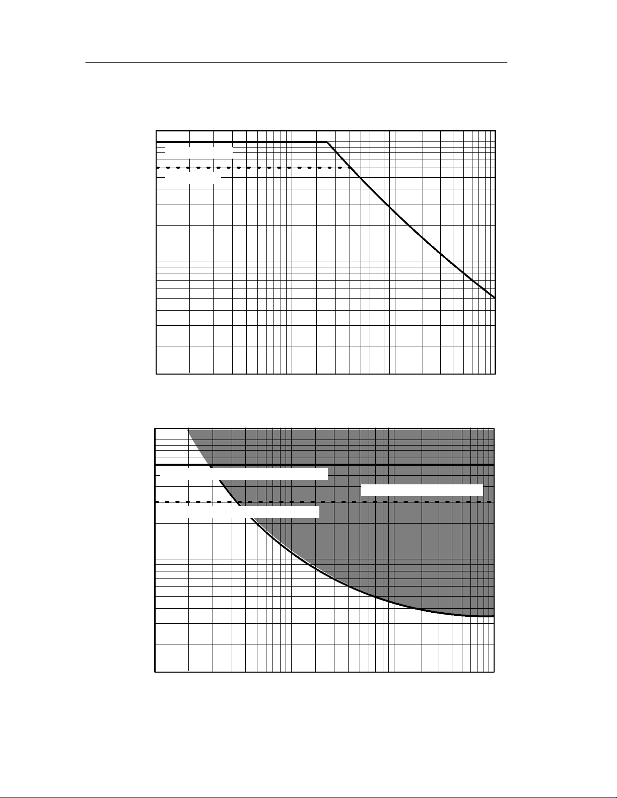
voltage and frequency limits specified in Figure 11b on page 18.
Avoid Electric Shock. To avoid inj ury or loss of life, do not connect or
disconnect probes or test leads while they are connected to a voltage
source.
Do Not Operate Without Covers. To avoid electric shock or fire hazard,
do not operate this product with covers or panels removed.
Do Not Operate in an Explosive Atmosphere. To avoid injury or fire
hazard, do not operate this product in an explosive atmosphere.
Keep Probe Surface Clean and Dry. To avoid electric shock and
erroneous readings, keep probe surface clean and dry.
Product Damage Precautions
Do Not Operate With Suspected Failures. If you suspect there is damage
to this product, have it inspected by qualified service personnel.
Do Not Immerse in Liquids. Clean the probe using only a damp cloth.
Refer to cleaning instructions on page 15.
P5102 Instruction Manual
iii
Page 8
General Safety Summary
Safety Terms and Symbols
Terms in This Manual. These terms may appear in this manual:
WARNING. Warning statements identify conditions or practices that
could result in injury or loss of life.
CAUTION. Caution statements identify conditions or practices that
could result in damage to this product or other property.
Terms on the Product. These terms may appear on the product:
DANGER indicates an injury hazard immediately accessible as you
read the marking.
WARNING indicates an injury hazard not immediately accessible as
you read the marking.
CAUTION indicates a hazard to property including the product.
Symbols on the Product. These symbols may appear on the product:
DANGER
High Voltage
Protective Ground
(Earth) Terminal
ATTENTION
Refer to Manual
Double
Insulated
Certifications and Compliances
Compliances. Consult the product specifications for Overvoltage
Category and Safety Class.
Overvoltage Category. Overvoltage categories are defined as follows:
CAT III: Distribution level mains, fixed installation
iv
CAT II: Local level mains, applianc es, portable equipment
CAT I: Signal level , special equipment or parts of equipment,
telecommunication, electronics
P5102 Instruction Manual
Page 9

Features and Accessories
The P5102 is a high-voltage passive probe designed for use with
TekScope THS700 series instruments. The probe features a floating
common and is ideal for measuring and troubleshooting power
supplies and high-voltage devices. The probe provides 10X
attenuation of signals up to 1000 V
to 100 MHz. The P5102 probe is certified to international safety
standards.
The P5102 probe has features and accessories to make high-voltage
measurements safer and easier. Please take a moment to familiarize
yourself with these features and accessories and their uses.
WARNING. Do not substitute accessories from other products for
those provided with the P5102. The accessories for the P5102 have
been safety tested. The use of non-tested accessories may cause
injury.
RMS
and derated performance up
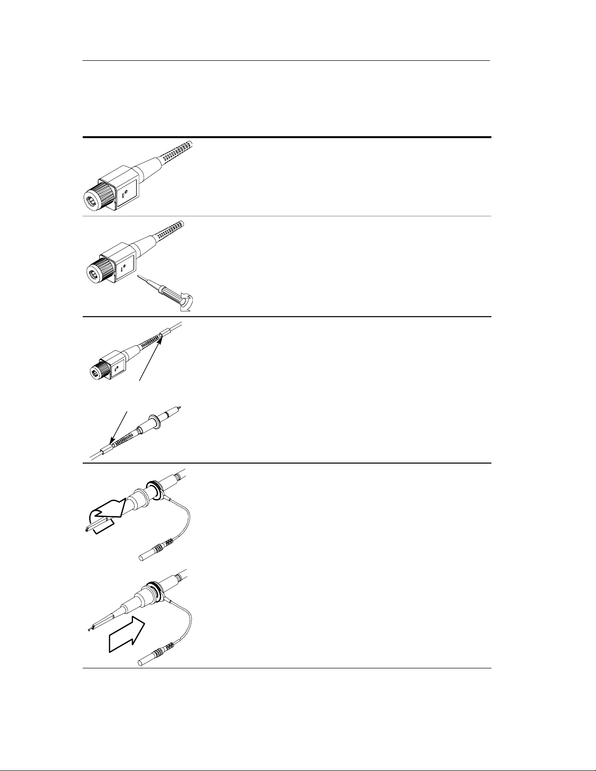
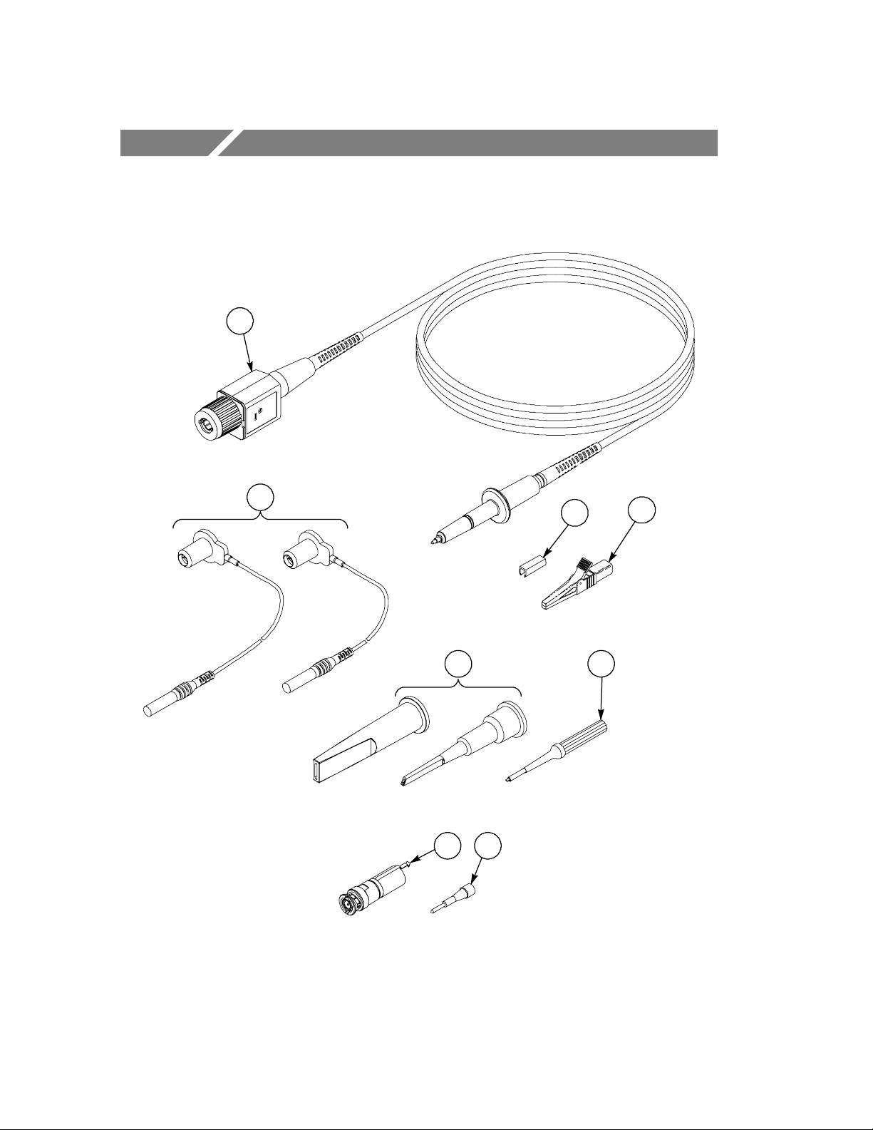
P5102 Features and Standard Accessories
Finger
Guard
Probe
Common
6-32 Probe Tip
Probe Body -- The P5102 probe body is designed for personal
safety, ergonomic comfort, and signal fidelity.
The finger guard provides protection when the hook tips are not being
used. Keep your fingers behind the finger guard whenever possible to
reduce the risk of a shock from the circuit under test.
The probe tip is a 6--32 threaded post that accepts both standard and
optional accessories.
Keep the probe body and accessories clean to reduce the risk of shock
due to surface conduction.
P5102 Instruction Manual
1
Page 10
Features and Accessories
P5102 Features and Standard Accessories (Cont.)
Compensation Box -- The compensation box contains low- and
high-frequency compensation adjustments. The high-frequency adjustments are accessible by removing the compensation box cover. Refer
to Adjustment Procedures on page 7.
Adjustment Tool -- Use the supplied adjustment tool for probe
compensation adjustments. Do not use metallic or conductive tools
while making adjustments.
Color Markers -- The matching markers help you identify probe
inputs at a glance. Clip one marker near the probe head and the
matching marker near the compensation box as shown.
Matching
Markers
Small Hook Tip -- Use the small hook tip for making connections to
small conductors such as component leads.
Install the small hook tip by sliding it over the body of the probe and
screwing it onto the threaded probe tip.
To use the tip, hold the probe body and pull the tip shield back. Hook
the tip onto the circuit and release the shield. The hook tip will firmly
hold the conductor under test.
2
P5102 Instruction Manual
Page 11

P5102 Features and Standard Accessories (Cont.)
Large Hook Tip -- Use the large hook tip when working with larger
components such as bolt terminals and buss bars typically found in
power distribution equipment.
Install the large hook tip by sliding it over the body of the probe and
screwing it onto the threaded probe tip.
To use the tip, hold the probe body and pull the tip shield back. Hook the
tip onto the circuit and release the shield. The hook tip will firmly hold the
conductor under test.
Features and Accessories
Common Leads -- The P5102 probe comes with a long and a short
floating common lead. Both common leads connect to a removable
crocodile clip.
Attach the common lead to the probe body by inserting the probe head
into common lead as shown.
The length of the common lead directly impacts the fidelity of high-frequency signals. The longer the common lead, the more the signal will
be distorted. For more information about the common lead and signal
quality, go to page 5.
Crocodile Clip -- The large crocodile clip attaches to the insulated
banana connector on the common leads.
WARNING. For safe electrical connections, use the crocodile clip
provided. Do not attempt to substitute the crocodile clip with any
other accessory.
P5102 Instruction Manual
3
Page 12

Features and Accessories
P5102 Optional Accessories
Probe Tip Extender (P6000) -- Use the probe tip extender to con-
nect the probe to larger test sockets located in equipment or on printed
circuit boards.
Connect the probe tip extender by screwing it onto the threaded
probe tip.
Ground
Clip
Probe
Common
Probe-to-BNC Adapter -- Use the probe-to-BNC adapter to
connect the probe directly to BNC connectors. The adapter is
recommended for use when verifying or adjusting the probe.
Attach the adapter by pressing it onto the 6-32 probe tip and making
sure that the ground clip makes contact with the probe common.
WARNING. Do not connect the adapter to a floating or high-voltage
source. The BNC adapter is only rated to 500 V (DC + peak AC)
with the probe common connected to earth ground.
4
P5102 Instruction Manual
Page 13
Operating Basics
To get guaranteed performance from the P5102 probe, ple ase read
and apply the information in this section.
Observe Voltage Derating Information
WARNING. To avoid personal injury, do not handle the probe when
the common lead is connected to a source that is above the voltage
and frequency limits specified in Figure 11b on page 18.
To avoid personal injury or damage to the probe, do not connect the
probe input to a source that is above the maximum non-destructive
input voltage and frequency limits given in Figure 11a on page 18.
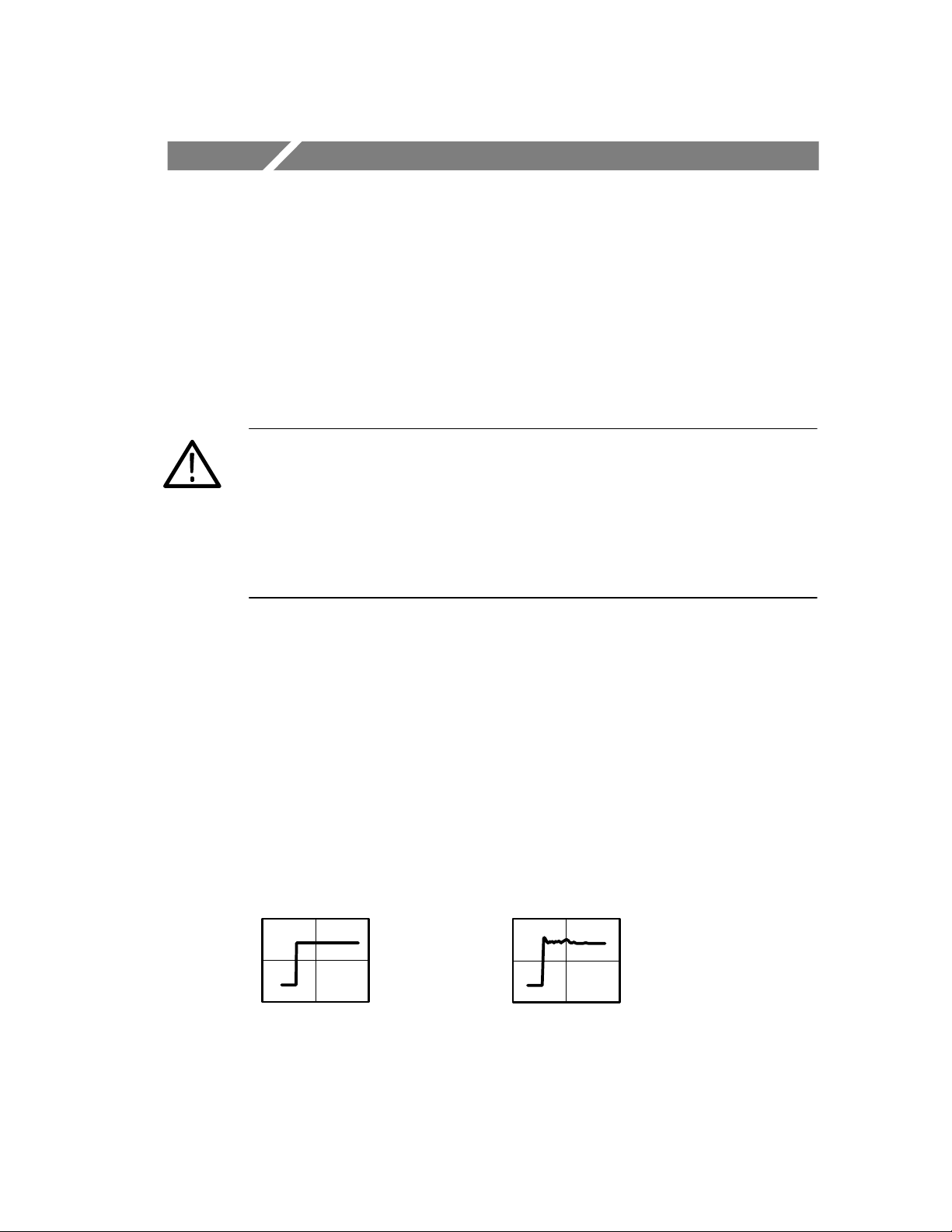
Common Lead Length
Always use as short a common lead as possible between the probe
head and circuit common for high frequency or fast rise time signals.
The input capacitance of the probe and the series inductance added
by the probe tip and common lead can result in a resonant circuit;
this circuit may cause parasitic “ringing” visible within the
bandwidth of your oscilloscope. Refer to Figure 1.
6-inch Common 18-inch
Figure 1: Waveform Distortion from Common Lead Length
Common
P5102 Instruction Manual
5
Page 14

Operating Basics
Parasitic ringing is not a concern when the probe is used with low
frequency or slow rise time signals and is not apparent if the
frequency content is beyond the bandwidth of the oscilloscope.
Probe Loading
When you touch your probe tip to a circuit element, you are
introducing a new resistance, capacitance, and inductance into the
circuit. Refer to Figure 2.
R
source
Probe C
11.2 pF
in
V
source
L
(common lead)
cl
Probe R
5MΩ
in
Figure 2: Probe Loading Equivalent Circuit
Frequency and impedance of the source determine how much the
probe loads the circuit you are measuring. As the frequency of the
source starts to increase beyond 1 kHz, the input impedance of the
probe begins to decrease. The lower the impedance of the probe
relative to that of the source, the more the probe loads the circuit
under test. Refer to Figure 12 on page 19 for a graph of frequency
versus input impedance.
The probe has virtually no loading effect on sources with relatively
low impedance and low frequency.
6
P5102 Instruction Manual
Page 15

Adjustment Procedures
The low-frequency (LF) compensation of the P5102 probe must be
checked every time the probe is connected to a different oscilloscope
input.
The high-frequency (HF) compensation should be checked if the
probe was repaired or fails to meet rated bandwidth specifications.
Check the probe using the performance verification procedures on
page 13 to determine if adjustment is required.
LF Compensation
Before taking any measurements with the probe, first check the LF
compensation of the probe and adjust it to match the channel input it
is connected to.
1. Connect the probe to the Probe Comp signal on your TekScope
instrument and then press AUTORANGE. See Figure 3.
Ch 1
Probe reference lead to
ProbetiptoPROBECOMP
AUTORANGE
Figure 3: LF Compensation Setup
P5102 Instruction Manual
7
Page 16

Adjustment Procedures
2. Compensate the probe by adjusting the trimmer in the probe
compensation box so that the corners of the signal are square. See
Figure 4.
LF
Figure 4: LF Compensation Adjustment
≈1 kHz
HF Compensation
To compensate the probe for high frequencies, you will need a
properly terminated signal source that has the characteristics given in
Figure 5. Refer to Table 1 on page 13 for a complete list of required
test equipment.
1MHz
1Vpp
Figure 5: Signal Source Characteristics for HF Compensation
tr<1 ns
90%
10%
To access the HF adjustments of the probe, you must open the cover
of the compensation box using the procedure that follows.
8
P5102 Instruction Manual
Page 17

Adjustment Procedures
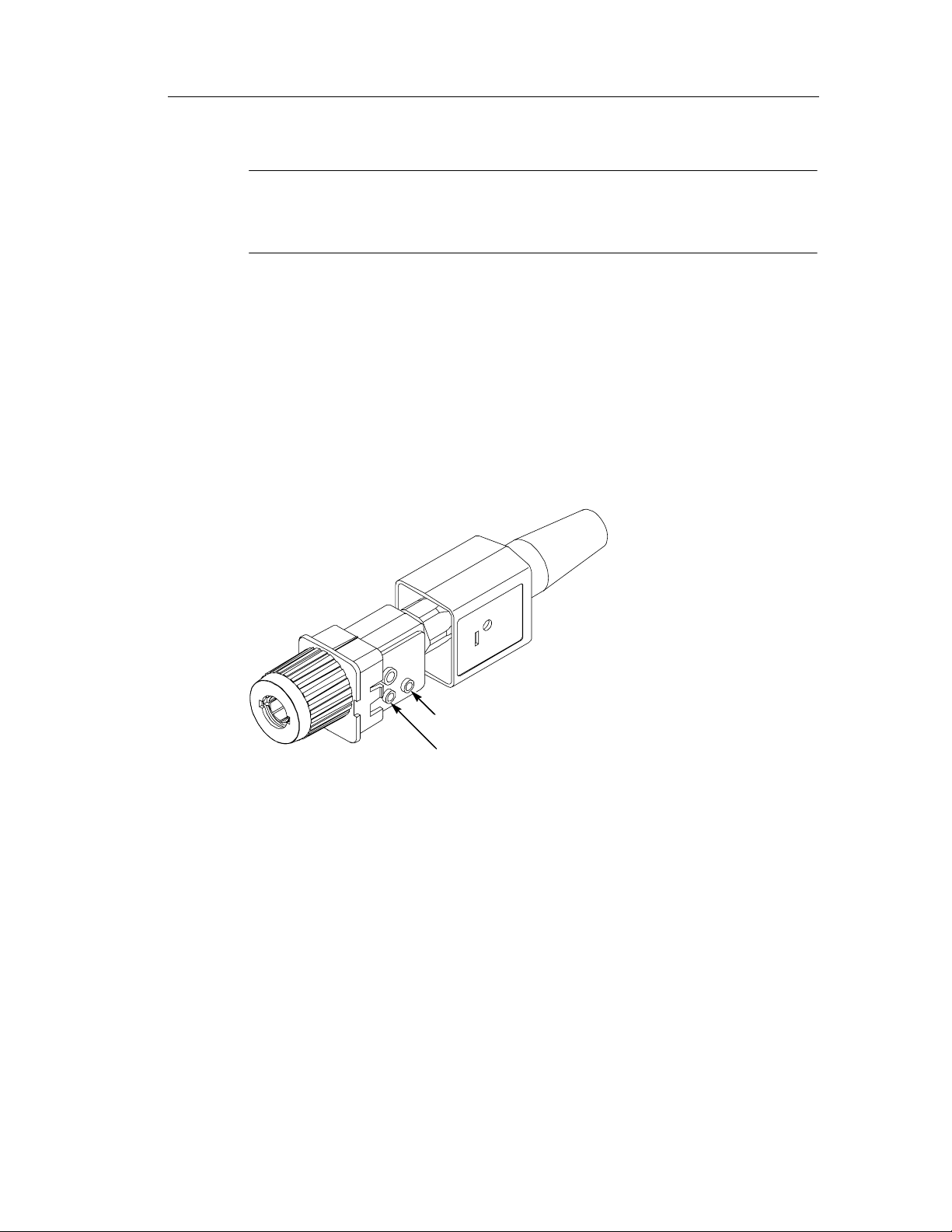
Opening the Compensation Box
NOTE. This procedure should be performed by qualified service
personnel only.
To open the cover, obtain two small screwdrivers and use them to
unlatch the tab as shown in Figure 6.
WARNING. Avoid damaging the tab. A damaged tab will allow the
cover to easily separate and expose the user to the electrical
potential of the common connection.
To avoid damaging the tab, do not attempt to press on the tab
through the hole in the cover where it latches. In the event of a
damaged tab, replace the probe.
1. Insert the flat blade of small screwdriver (A) into the location
shown in Figure 6. Insert the blade until it stops against the back
of the tab.
B
Tab
Insert up to the Tab
A
Figure 6: Opening the Compensation Box
P5102 Instruction Manual
9
Page 18

Adjustment Procedures
2. While holding screwdriver (A) in place, insert small screwdriver
(B) between the ridge on the front of the compensation box and
the edge of the cover.
3. Gently twist the blade of screwdriver (B) to separate the cover
and unlatch the tab.
4. After unlatching the tab, slide the cover back to expose the
internal adjustments.
HF Compensation Procedure
After opening the compensation box, perform the following
procedure to compensate the probe for high frequencies.
1. Connect a 50 Ω feedthrough termination to the positive going
FAST RISE output of the calibration generator. See Figure 7.
Calibration
Generator
FAST RISE Output
50 Ω Termination
Probe-to-BNC Adapter
P5102 Probe
Figure 7: HF Compensation Setup
2. Refer to page 4 and use the optional probe-to-BNC adapter to
connect the probe to the termination.
10
3. Set the Calibration Generator to 1 MHz.
4. Set the PULSE AMPLITUDE to 0.5 V
.
P-P
P5102 Instruction Manual
Page 19
Adjustment Procedures
NOTE. If you have changed the default setting for the probe type,
access the vertical menu of the TekScope instrument and return the
setting to 10X.
5. Set the oscilloscope to 100 mV/division.
6. Set the oscilloscope averaging to 4.
7. Set the oscilloscope to 10 ns/div (100 ns, X10 magnification)
Adjust the oscilloscope as necessary to view the leading edge of
the waveform.
8. Locate the HF1 and HF2 adjustments. See Figure 8.
HF1
HF2
Figure 8: HF Compensation Adjustments
9. Preset HF1 counterclockwise and HF2 clockwise.
10. Adjust HF2 for flatness and adjust HF1 for the best front corner.
SeeFigure9.BecauseHF1 and HF2 interact, readjust HF2 and
HF1 as necessary to achieve the best rise time with the smallest
aberrations.
P5102 Instruction Manual
11
Page 20

Adjustment Procedures
6%
Aberrations
Figure 9: HF Compensation Regions of Fast Rise Signal
HF2
(20 ns)
HF1
(10 ns)
11. After compensating the HF, carefully slide the cover bac k until
the tab latches securely into place.
12
P5102 Instruction Manual
Page 21

Performance Verification
Oscill
Calibrati
Use the procedure in this section to verify that the P5102 probe
meets the warranted bandwidth specification highlighted with
boldface type in the Specifications section on page 17. The steps of
this procedure must be performed in the order gi ven using a THS720
TekScope instrument and other equipment that meets the minimum
requirements listed in Table 1.
Table 1: Required Test Equipment
Description
Oscilloscope Use a THS720 only. The
Calibration Generator
(for HF adjustment only)
Leveled Signal Generator 50 kHz to 250 MHz
Termination, 50 Ω
feedthrough
Adapter, probe tip to BNC ProbetiptomaleBNC Tektronix part number
Minimum Requirements Example
THS720
probe is optimized to match
the input characteristics and
bandwidth of the THS720
≤1 ns rise time square wave Wavetek 9100 Universal
Calibration System with
oscope
Module (Option 250)
50 Ω male to female BNC
Tektronix part number
011-0049-01
013-0291-00
NOTE. Compensate the probe for LF before performing this
procedure. The LF compensation procedure begins on page 7.
on
If the probe does not meet the bandwidth requirement of this
procedure, perform the adjustments beginning on page 7 and retest.
P5102 Instruction Manual
13
Page 22

Performance Verification
1. Connect the test setup as shown in Figure 10.
Leveled
Sine Wave
Generator
50 Ω Termination
P5102 Probe
Test
Oscilloscope
Output
Probe Tip to
BNC Adapter
Figure 10: Bandwidth Test Setup
2. Set the leveled signal generator output frequency to 1 MHz.
NOTE. If you have changed the default setting for the probe type,
access the vertical menu of the TekScope instrument and return the
setting to 10X.
14
3. Set the oscilloscope to 50 mV/division. (The effective setting
with the 10X attenuation of the probe is 500 mV/division.)
4. Adjust the Leveled Signal Generator for a display exactly 6
divisions peak-to-peak.
5. Increase the Leveled Signal Generator frequency until the display
is 4.2 divisions peak-to-peak. (This represents the . 707 or
half-power amplitude.)
6. Note that the frequency is greater than 100 MHz.
P5102 Instruction Manual
Page 23

Maintenance
This section contains information necessary for the maintenance and
repair of the P5102 probe.
NOTE. The P5102 probe has no replaceable components. Accessory
parts may be ordered as indicated in the replaceable parts list.
Cleaning Instructions
Clean the probe using a soft cloth dampened with a mild detergent
and water solution. Do not use any other chemicals or abrasives.
Customer Support
Refer to Contacting Tektronix at the front of this manual for a listing
of the various ways to contact Tektronix, Inc. for operational and
service support of this product.
P5102 Instruction Manual
15
Page 24

Maintenance
Preparation for Shipment
If you need to ship your probe, pack it carefully to prevent damage
while in transit. If the original pa ckaging is unfit for use or not
available, use the following packaging guidelines:
1. Use a corrugated cardboard shipping carton having inside
dimensions at least one inch greater than the probe dimensions.
The box should have a carton test strength of at least 200 pounds.
2. Put the probe into a plastic bag or wrap to protect it from
dampness in transit.
3. Place the probe into the box and stabilize it with light
packing material.
4. Seal the carton with shipping tape.
16
P5102 Instruction Manual
Page 25

Specifications
The warranted specifications of Table 2 that appear in boldface type
are specifications checked in the Performance Verification section.
Specifications that are not warranted are typical (Tables 3 and 4) and
are provided as general information for your convenience.
The specifications apply to a P5102 probe installed on a Tektronix
THS720 oscilloscope. The instrument must have a warm-up period
of at least 10 minutes and be in an environment that does not exceed
the limits described in Table 5.
Table 2: Warranted Electrical Specifications
Attenuation
(DC coupled system)
Bandwidth
(--3 dB, DC coupled system)
Maximum Rated Input Voltage IEC 1010-1 Installation C ategory
Between probe tip and probe common
or between probe tip and earth ground
(Refer to Figure 11a for derating with
frequency)
Between probe common and earth ground
(Refer to Figure 11b for safe-handling limits
for overload and RF)
Safety
X10, ±2%
DC to 100 MHz (THS720)
DC to 60 MHz (THS710)
I II III
1000
600 600 300
UL 3111--1 First Edition
CSA 22.2 No. 1010.1--92, Series M89
EN 61010-1
EN 61010-2-031
1000 600
IEC Installation Category Category II
IEC Pollution Degree Degree 2
IEC Safety Class Class 2
(Double/Reinforced Insulation)
P5102 Instruction Manual
17
Page 26
Specifications
a. Maximum non-destructive input voltage (probe tip to common or earth ground)
1000V
500V
Voltage
)
(V
RMS
100V
50V
b. Maximum safe-handling limits (probe common to earth ground)
DC or 0
Category I & II
Category III
100k
500k
1M 5M 10M 50M 100M
Frequency (Hz)
1000V
Category I & II maximum voltage limit
Category III maximum voltage limit
DC or 0 10M1M 5M 50M500k100k
Frequency (Hz)
Voltage
(V
RMS
500V
)
100V
50V
Figure 11: Maximum Voltage Derating Curves (V
RF burn risk area (shaded)
, DC Coupled)
RMS
100M
18
P5102 Instruction Manual
Page 27

Table 3: Typical Electrical Characteristics
Specifications
Rise Time (System)
Checked using optional BNC adapter
Input Resistance (System)
3.5 ns (THS720)
5.8 ns (THS710)
5MΩ
SeeFigure12
Input Phase (System) (See Figure 13)
Compensation Range 23 pF to 27 pF
Input Capacitance (System)
11.2 pF
Probe connected to instrument and properly
compensated. Checked at 1 MH z
10 MΩ
1MΩ
100 kΩ
10 kΩ
1kΩ
100 Ω
1kDC or 0
10 k 100 k 1 M 10 M 100 M
Figure 12: Typical Input Impedance
Frequency (Hz)
P5102 Instruction Manual
19
Page 28

Specifications
-10_
-20_
-30_
-40_
-50_
-60_
-70_
-80_
-90_
10 k 100 k 1 M 10 M 100 M1kDC or 0
Figure 13: Typical Input Phase
Frequency (Hz)
20
P5102 Instruction Manual
Page 29

Table 4: Typical Mechanical Characteristics
Specifications
Net Weight
(including accessories)
Cable Length 2 m (6.56 ft)
0.26 kg (0.57 lb)
Table 5: Environmental Specifications
Temperature Operating: --15 °Cto+55°C
(+5 °F to +131 °F)
Nonoperating: --62 °Cto+85°C
(--79.6 °F to +185 °F)
Humidity Nonoperating and operating; five cycles (120 hr. total)
+40 °C or below: ≤95% relative humidity
(+104 °F or below)
+41 °Cto+50°C: ≤75% relative humidity
(+105 °F to +122 °F)
Transportation Tektronix Standard 062-9537-00 Revision C
P5102 Instruction Manual
21
Page 30
Replaceable Parts
1
6
2
Standard Accessories
7
8
3
45
Figure 14: P5102 Replaceable Parts
22
Optional Accessories
P5102 Instruction Manual
Page 31

3
3
4
-
-
1
2
7
5
-
-
0
4
2
C
L
IPC
A
B
LEM
K
R
:YE
L
L
O
W
P
L
A
S
T
I
C
0
JR0
5
O
r
d
e
r
b
y
d
e
s
c
r
i
p
t
i
o
n
3
3
4
4
0
4
6
1
0
0
1CL
I
P
C
A
B
LEM
K
R
Y
E
L
L
O
W
P
L
A
S
T
I
C
C
L
I
P
E
L
E
C
:
C
R
O
C
O
D
I
L
E
8
2
M
M
L4M
M
J
R
T
K
2
4
8
3
O
d
b
y
d
i
i
on
X
K
0
8
1
5
0
1
3
0
2
9
0
0
1
1CL
L
L
L
H
O
O
K
T
IPS
E
T
:
H
O
O
K
T
IPA
S
S
Y
L
A
R
G
E
A
N
D
S
M
A
L
L
T
K
2
4
6
9
0
1
3
0
2
9
0
0
1
L
L
L
,
,
pt
escr
Replaceable Parts
Mfr. Part No.
Mfr.
Code
12345 Name & Description
STANDARD ACCESSORIES
Order by description
0JR05
CLIP, CABLE MKR: RED, PLASTIC
er
r
05
0
,
:
,
Order by description
0JR05
CLIP, CABLE MKR: GREEN, PLASTIC
XK--081
TK2483
,4MM
E, 82MM
EC: CROCODI
IP,E
TK2469 013029001
ARGE AND SMA
SCREWDRIVER: ADJUSTMENT TOOL
HOOKTIP, SET: HOOKTIP ASSY,
LEAD SET ASSY: COMMON, P5102, 1) 18.0 L 1) 6.0 L
MANUAL, TECH: INSTRUCTIONS, P5102 80009 0709294XX
OPTIONAL ACCESSORIES
Qty
Serial No.
Effective Dscont
Part No.
Tek t r o n ix
-- -- -- -- -- -- -- -- -- -- -- 1 PROBE, HI VOLTAGE: F L OATING, 10X, 100 MHZ, P5102
No.
Index
Fig. &
14--1
2
-- 2 334--1275--02
2
334--1275--04
2
334--1275--05
1
344--0461--00
-- 3
1
See Opt. Acc.
-- 4
1
013--0290--01
-- 5
1
196--3424--00
-- 6
070--9294--XX 1
-- 7 206--0060--00 1 TIP, PROBE: P6000 80009 206006000
--8 013--0291--00 1 ADAPTER, PROBE: PROBE TO BNC 80009 013029100
--4 003--1433--01 1 SCREWDRIVER: ADJU STMENT TOOL, PKG OF 5 80009 003143301
23P5102 Instruction Manual
Page 32

Replaceable Parts
D--4300 ESSEN 11 (W GERMANY)
MESSTECHNISCHE WERKE
CATHOSTRASSA 7
BEAVERTON OR 97077--0001
PO BOX 500
CROSS INDEX - MFR. CODE NUMBER TO MANUFACTURER
24
Mfr.
Manufacturer Address City, State, Zip Code
Code
TRIQUEST CORP
0JR05
TK2483 HEINRICH C KOSMEIER
GMBH--ESSEN
TK2469 UNITREK CORPORATION 3000 LEWIS & CLARK HWY VANCOUVER WA 98661
80009 TEKTRONIX INC 14150 SW KARL BRAUN DR
P5102 Instruction Manual
 Loading...