


Instructions
P5100
2500 V 250 MHz Oscilloscope Probe
070-8151-04
Warning
The servicing instructions are for use by qualified
personnel only. To avoid personal injury, do not
perform any servicing unless you are qualified to
do so. Refer to all safety summaries prior to
performing service.
www.tektronix.com

Copyright © Tektronix, Inc. All rights reserved.
Tektronix products are covered by U.S. and foreign patents, issued and
pending. Information in this publication supercedes that in all previously
published material. Specifications and price change privileges reserved.
Tektronix, Inc., 14200 SW Karl Braun Drive, Beaverton, OR 97077
TEKTRONIX and TEK are registered trademarks of Tektronix, Inc.

WARRANTY
Tektronix warrants that the products that it manufactures and sells will be free from defects
in materials and workmanship for a period of one (1) year from the date of shipment. If a
product proves defective during this warranty period, Tektronix, at its option, either will
repair the defective product without charge for parts and labor, or will provide a
replacement in exchange for the defective product.
In order to obtain service under this warranty, Customer must notify Tektronix of the
defect before the expiration of the warranty period and make suitable arrangements for the
performance of service. Customer shall be responsible for packaging and shipping the
defective product to the service center designated by T ektronix, with shipping charges
prepaid. Tektronix shall pay for the return of the product to Customer if the shipment is to
a location within the country in which the Tektronix service center is located. Customer
shall be responsible for paying all shipping charges, duties, taxes, and any other charges for
products returned to any other locations.
This warranty shall not apply to any defect, failure or damage caused by improper use or
improper or inadequate maintenance and care. Tektronix shall not be obligated to furnish
service under this warranty a) to repair damage resulting from attempts by personnel other
than Tektronix representatives to install, repair or service the product; b) to repair damage
resulting from improper use or connection to incompatible equipment; c) to repair any
damage or malfunction caused by the use of non-Tektronix supplies; or d) to service a
product that has been modified or integrated with other products when the effect of such
modification or integration increases the time or difficulty of servicing the product.
THIS WARRANTY IS GIVEN BY TEKTRONIX IN LIEU OF ANY OTHER
WARRANTIES, EXPRESS OR IMPLIED. TEKTRONIX AND ITS VENDORS
DISCLAIM ANY IMPLIED WARRANTIES OF MERCHANTABILITY OR
FITNESS FOR A PARTICULAR PURPOSE. TEKTRONIX’ RESPONSIBILITY
TO REPAIR OR REPLACE DEFECTIVE PRODUCTS IS THE SOLE AND
EXCLUSIVE REMEDY PROVIDED TO THE CUSTOMER FOR BREACH OF
THIS WARRANTY. TEKTRONIX AND ITS VENDORS WILL NOT BE LIABLE
FOR ANY INDIRECT, SPECIAL, INCIDENTAL, OR CONSEQUENTIAL
DAMAGES IRRESPECTIVE OF WHETHER TEKTRONIX OR THE VENDOR
HAS ADVANCE NOTICE OF THE POSSIBILITY OF SUCH DAMAGES.


Table of Contents
Contacting Tektronix ii................................
General Safety Summary iii............................
Features and Accessories 1.............................
Operating Basics 5...................................
Maximum Non-destructive Input Voltage 5.................
Grounding the Probe 5.................................
Ground Lead Length 5.................................
Adjustment Procedures 9..............................
Low Frequency (LF) Probe Compensation 9................
DC Gain and High Frequency (HF) Compensation 10.........
Gain Adjustment (DC Accuracy) 11....................
High-Frequency (HF) Adjustment 12....................
Performance Verification 15............................
DC Accuracy Check 16.................................
Bandwidth Check 17....................................
Maintenance 19.......................................
Cleaning 19...........................................
Preparation for Shipment 19..............................
Replacing Probe Parts 20................................
Specifications 23......................................
Replaceable Parts 29...................................
P5100 Instructions
i

Contacting Tektronix
Phone 1-800-833-9200*
Address Tektronix, Inc.
Department or name (if known)
14200 SW Karl Braun Drive
P.O. Box 500
Beaverton, OR 97077
USA
Web site www.tektronix.com
Sales
support
Service support
Technical
support
* This phone number i s toll free in North America. After office
hours, please leave a voice mail message.
Outside North America, contact a Tektronix sales office or
distributor; see the Tektronix web site for a list of offices.
1-800-833-9200, select option 1*
1-800-833-9200, select option 2*
Email: techsupport@tektronix.com
1-800-833-9200, select option 3*
1-503-627-2400
6:00 a.m. -- 5:00 p.m. Pacific time
ii
P5100 Instructions

General Safety Summary
Review the following safety precautions to avoid injury and prevent
damage to this product or any products connected to it. To avoid
potential hazards, use this product only as specified.
Only qualified personnel should perform service procedures.
To Avoid Fire or Personal Injury
Connect and Disconnect Properly. Connect the probe output to the
measurement instrument before connecting the probe to the circuit
under test. Disconnect the probe input and the probe ground from the
circuit under test before disconnecting the probe from the
measurement instrument.
Observe All Terminal Ratings. To avoid fire or shock hazard, observe all
ratings and markings on the product. Consult the product manual for
further ratings information before making connections to the product.
Do not apply a potential to any terminal that exceeds the maximum
rating of that terminal.
Connect the ground lead of the probe to earth ground only.
Avoid Exposed Circuitry. Do not touch exposed connections and
components when power is present.
Do Not Operate With Suspected Failures. If you suspect there is damage
to this product, have it inspected by qualified service personnel.
Do Not Operate in Wet/Damp Conditions.
Do Not Operate in an Explosive Atmosphere.
Keep Product Surfaces Clean and Dry.
P5100 Instructions
iii

General Safety Summary
Safety Terms and Symbols
Terms in This Manual. These terms may appear in this manual:
WARNING. Warning statements identify conditions or practices that
could result in injury or loss of life.
CAUTION. Caution statements identify conditions or practices that
could result in damage to this product or other property.
Terms on the Product. These terms may appear on the product:
DANGER indicates an injury hazard immediately accessible as you
read the marking.
WARNING indicates an injury hazard not immediately accessible as
you read the marking.
CAUTION indicates a hazard to property including the product.
Symbols on the Product. These symbols may appear on the product:
WARNING
Risk of Electric
Shock
Protective Ground
(Earth) Terminal
CAUTION
Refer to Manual
Double
Insulated
iv
P5100 Instructions
Features and Accessories
The P5100 is a 100X, 2500 V (DC + peak AC), 1000 V CAT III
oscilloscope probe that provides 250 MHz performance and is
certified to international safety standards. The P5100 probe is
compatible with all general purpose oscilloscopes and with Tektronix
oscilloscopes that automatically detect 100X probe attenuation and
display the correct scale readout. The P5100 probe is designed for
ground-referenced measurements only.
WARNING. Do not substitute accessories from other products for
those provided with the P5100. The accessories for the P5100 have
been safety tested, and the use of non-tested accessories may cause
injury or death.
To reduce risk of electric shock, keep your fingers behind the finger
guard on the probe body. Place your fingers in front of the finger
guard only when retracting the hook-tip accessory.
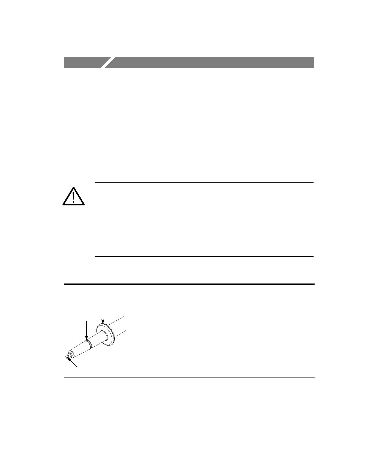
P5100 Features and Standard Accessories
Finger
Guard
Ground
Ring
6-32 Probe Tip
Probe Body -- The P5100 probe body is designed for personal
safety, ergonomic comfort, and signal fidelity.
The probe body ground ring connection allows a short ground
connection for optimal signal fidelity.
The probe tip is a 6--32 threaded post that accepts both standard and
optional accessories.
Keep the probe body and accessories clean and dry to reduce the risk
of shock due to surface conduction. Refer to page 19 for cleaning
instructions.
P5100 Instructions
1
Features and Accessories
P5100 Features and Standard Accessories (Cont.)
Compensation Box -- The P5100 compensation box contains low-
and high-frequency compensation adjustments as well as a
gain adjustment.
The P5100 is compatible with Tektronix oscilloscopes that automatically detect and display the 100X attenuation factor of the probe.
(If you have an older instrument with a lit vernier indicator, the 10X
position will light. Multiply the reading by a factor of 10 to get the true
Readout Pin
value.)
Ground Leads -- The P5100 probe comes with a long and a short
ground lead. Both ground leads connect to a removable crocodile clip.
Attach the ground lead to the probe body by inserting the probe head
into the ground lead as shown.
The length of the ground lead directly impacts the fidelity of high-frequency signals. The longer the ground lead, the more the signal will
be distorted. For more information about the ground lead and signal
quality, go to page 5.
Crocodile Clip -- The large crocodile clip attaches to the insulated
banana connector on the long ground lead.
Small Hook Tip -- Use the small hook tip for making connections to
small conductors such as component leads.
Install the small hook tip by sliding it over the body of the probe and
screwing it onto the threaded probe tip.
To use the tip, hold the probe body and pull the tip shield back. Hook
the tip onto the circuit and release the shield. The hook tip will firmly
hold the conductor under test.
2
P5100 Instructions
P5100 Features and Standard Accessories (Cont.)
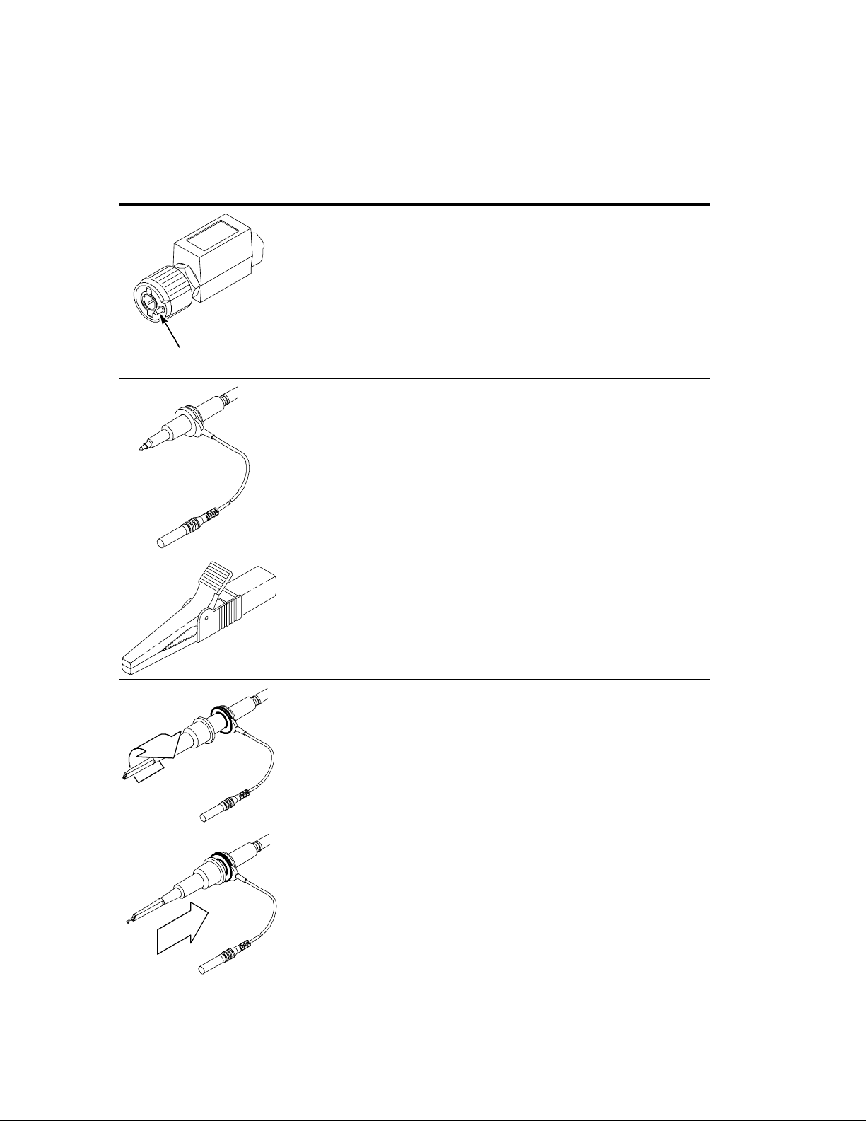
Large Hook Tip -- Use the large hook tip when working with larger
components such as bolt terminals and buss bars typically found in
power distribution equipment.
Install the large hook tip by sliding it over the body of the probe and
screwing it onto the threaded probe tip.
To use the tip, hold the probe body and pull the tip shield back. Hook the
tip ontothe circuit and releasethe shield. The hooktip will firmly hold the
conductor under test.
Features and Accessories
Color Marker
Bands
Color Marker Bands -- The color marker bands help you identify
multiple probes in the circuit under test.
Clip the matching bands onto the cable at the probe head and compensation box to help identify probe channels at a glance.
Adjustment Tool -- Use the adjustment tool for probe compensation
adjustments. Do not use metallic or conductive tools while making
adjustments.
P5100 Instructions
3
Features and Accessories
P5100 Optional Accessories
Ground
Clip
Ground
Ring
Probe Tip to BNC Adapter -- Use the probe tip to BNC adapter to
connect the probe directly to BNC connectors. The adapter is
recommended for use when verifying or adjusting the probe.
WARNING. The BNC adapter is rated to 500 V (DC + peak AC). Do
not attempt to use the adapter for high voltage testing.
Attach the adapter by pressing it onto the 6-32 probe tip and making
sure that the ground clip makes contact with the ground ring.
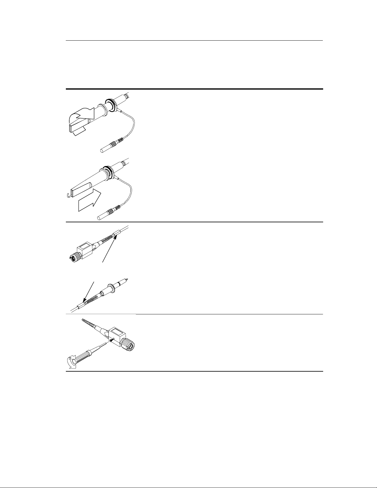
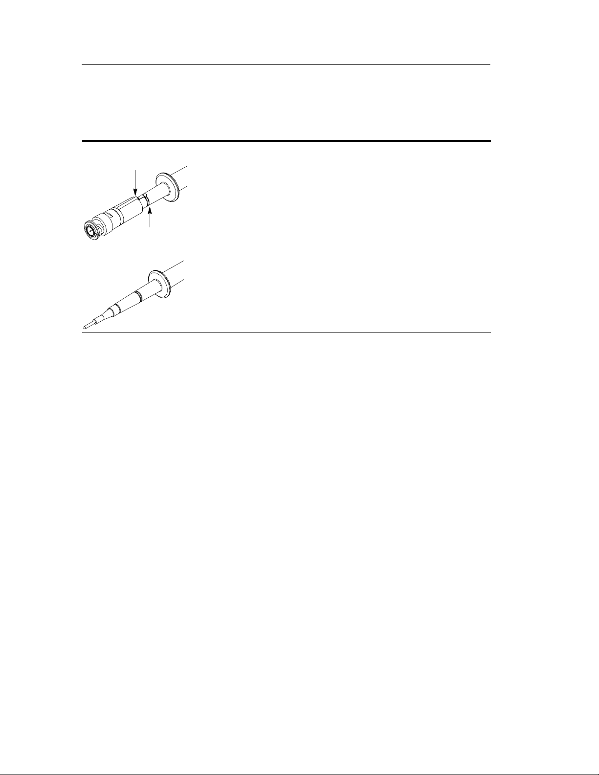
Rubber Spring Tip -- Use the rubber spring tip to connect the P5100
to larger test sockets located in equipment or on printed circuit boards.
Connect the rubber spring tip by screwing it onto the threaded
probe tip.
4
P5100 Instructions

Operating Basics
Users need to know this information to get guaranteed performance
from the P5100. For best results, please read and apply this
information.
Maximum Non-destructive Input Voltage
The P5100 is designed to be used in a high voltage environment;
however, the voltage input rating of the probe decreases as the
frequency of the applied signal increases. Please refer to the
Specifications section of this manual for the maximum input voltage
and frequency derating information.
Grounding the Probe
Connect the probe to the instrument and connect the ground lead to
ground before making any measurements. Be careful that no part of
the ground lead contacts voltage in the circuit under test. Except for
the probe tip and BNC center conductor, all accessible metal
(including the ground clip) is connected to the BNC shell.
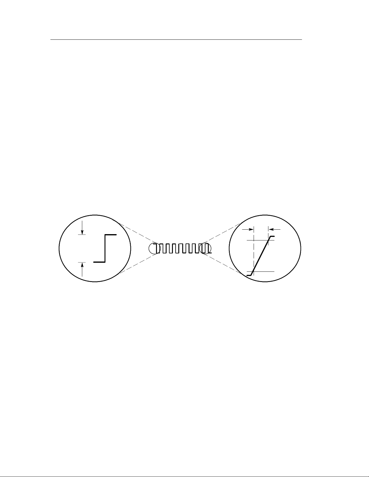
Ground Lead Length
Always use as short a ground lead as possible between the probe
head and circuit ground.
The series inductance added by the probe tip and ground lead can
result in a resonant circuit; this circuit may cause parasitic “ringing”
visible within the bandwidth of your oscilloscope. Refer to Figure 1.
P5100 Instructions
5

Operating Basics
Six-inch ground 18-inch ground
Chassis ground
(no ground lead)
Figure 1: Waveform Distortion from Ground Lead Length
“Ringing” is not a concern when the probe is used with low
frequency or long rise time signals.
When you touch your probe tip to a circuit element, you are
introducing a new resistance, capacitance, and inductance into the
circuit. Refer to Figure 2.
R
source
Probe C
2.75 pF
V
source
Probe R
10 MΩ
in
in
L
(Ground Lead)
gl
Figure 2: Probe Loading Equivalent Circuit
Ringing and rise time degradation can be masked if the frequency
content of the signal degradation is beyond the bandwidth of
the oscilloscope.
6
P5100 Instructions

Operating Basics
f
=
0
1
2π LC
The preceding equation shows that reducing the ground lead
inductance will raise the resonant frequency. If your measurements
are affected by ringing, you can lower the inductance of your ground
path (typically by shortening the ground lead) until the resonant
frequency is well above the frequency of your measurements.
P5100 Instructions
7

Operating Basics
8
P5100 Instructions

Adjustment Procedures
The low-frequency compensation of the P5100 must be checked
every time that the probe is connected to a different oscilloscope
input.
The DC gain and high-frequency compensation may require
readjustment if it is used on more than one oscilloscope; however,
before making these adjustments, perform a functional check to
determine if the adjustments are required.
Low Frequency (LF) Probe Compensation
A probe must be adjusted to match the input impedance of an
oscilloscope in the same way that an antenna must be matched to a
radio transmitter. If there is a mismatch between the two halves of
the system, excessive distortion will result.
Because of the attenuation of a 100X probe, a signal source of at
least 5 V peak-to-peak at 10 kHz is ideal (The PG506A Calibration
Generator HIGH AMPL output meets this requirement.): however,
the front panel calibrator on your oscilloscope may be adequate.
Connect the probe to the signal source to display the test signal on
your oscilloscope. To get a clear signal display, select the averaging
or high resolution mode on your oscilloscope. Compensate the
probe by adjusting LF on the probe compensation box so that the
corners of the square wave are square. See Figure 3.
LF
Figure 3: Coarse (LF) Compensation Adjustment
P5100 Instructions
10 kHz
9
Adjustment Procedures
DC Gain and High Frequency (HF) Compensation
Precision, or high-frequency, compensation is not a common user
adustment; however, precision compensation should be checked if
the probe was repaired or if any of the following conditions are true:
H the probe has excessive high-frequency aberrations
H the probe fails to meet rated bandwidth specifications
H you have installed the probe on an oscilloscope having an input
capacitance near the limits of the probe compensation range (See
Table 3 on page 24.)
To perform the high-frequency compensation adjustment you will
need a signal source that has all of the following characteristics:
tr<1 ns
1MHz
1 Vpp
H square-wave output at 1 MHz
H fast rise output with rise time less than 1 ns
H output properly terminated
The Tektronix PG506A Calibration Generator FAST RISE output
meets these requirements when properly terminated.
90%
10%
10
P5100 Instructions

Adjustment Procedures
Gain Adjustment (DC Accuracy)
NOTE. If you adjust the DC gain, you must readjust the low frequency
compensation; the DC gain and low frequency compensation
adjustments interact with each other.
1. Remove the top and bottom covers of the compensation box. To
remove the covers, insert a thin flat-blade screwdriver between
the shell covers and gently rotate the screwdriver to loosen the
covers.
2. Connect the probe to the unterminated STD output of the
calibration generator using the optional probe tip to BNC adapter.
SeeFigure4.
Calibration
Generator
STD AMP Output
Probe Tip to BNC Adapter
P5100 Probe
Figure 4: Gain Adjustment Setup
3. Set the calibration generator AMPLITUDE to 100 V.
4. Set the oscilloscope to 20 V/division (200 mV/division without
scale factor).
Test Oscilloscope
5. Adjust the oscilloscope to display two to five cycles of the
test signal.
P5100 Instructions
11

Adjustment Procedures
6. Locate the HF1, HF2,andDC Gain adjustments. See Figure 5.
Figure 5: P5100 Adjustment Locations
HF1
HF2
DC Gain
7. Adjust DC Gain for exactl y five divisions of signal amplitude at
the falling edges of the waveform. (The HIGH measurement
function of the oscilloscope may also be used to check DC gain).
8. Recheck the LF compensation.
High-Frequency (HF) Adjustment
1. Connect a 50 Ω feedthrough termination to the positive going
FAST RISE output of the calibrati on generator. See Figure 6.
12
P5100 Instructions

Calibration
Generator
Adjustment Procedures
Test Oscilloscope
FAST RISE Output
50 Ω Terminator
Probe Tip to BNC Adapter
P5100 Probe
Figure 6: HF Adjustment Setup
2. Using the optional probe tip to BNC adapter, connect the probe to
the termination.
3. Set the Calibration Generator to 1 MHz.
4. Set the PULSE AMPLITUDE to maximum.
5. Set the oscilloscope to 200 mV/division (2 mV/division without
scale factor).
6. Set the oscilloscope averaging to 8.
7. Set the oscilloscope to 20 ns/div. (Adjust the oscilloscope as
necessary to view the leading edge of the waveform.)
8. Adjust HF2 for long term flatness.
9. Adjust HF1 for a square leading edge. See Figure 7.
P5100 Instructions
13

Adjustment Procedures
Figure 7: HF Compensation Adjustments
HF2
HF1
14
P5100 Instructions

Performance Verification
Use these performance verification procedures to verify that the
P5100 meets the warranted specifications. These procedures should
be performed in the order given using a TDS460 oscilloscope with
the equipment recommended in Table 1.
NOTE. The probe must be low-frequency compensated before
performance can be verified.
If your P5100 fails to qualify under these conditions, perform the
adjustments starting on page 9 and retest.
Table 1: Recommended Test Equipment
Equipment Minimum R equirements
Recommended
Equipment
Oscilloscope 350 MH z Tektronix TDS460
Calibration Generator ≤1 ns rise time square wave
100 V square wave
Leveled Signal Generator 50 kH z to 250 MHz Tektronix SG503
Termination, 50 Ω
feedthrough
Adapter, BNC Female--to--female barrel Tektronix 103-0028-00
Adapter, probe tip to BNC Probe tip--to--male BNC Tektronix 013-0291-00
BNC cable, precision No substitute
1
Required for use with Tektronix SG503.
50 Ω male--to--female BNC
1
Tektronix PG506A
Tektronix 011-0049-01
Tektronix 012-0482-00
P5100 Instructions
15

Performance Verification
DC Accuracy Check
1. Connect the DC accuracy test setup as shown in Figure 8.
Calibration
Generator
STD AMP Output
Probe Tip to BNC Adapter
P5100 Probe
Test Oscilloscope
Figure 8: DC Accuracy Test Setup
2. Set the oscilloscope to 20 V/division (200 mV/division without
scale factor).
3. Set the Calibration Generator AMPLITUDE to 100 V.
4. Adjust the VARIABLE (OUT) control on the Calibration
Generator for a signal exactly five divisions in amplitude.
NOTE.TheAmplitude measurement selection on the oscilloscope
may be used to confirm the signal amplitude.
5. Note the percent error displayed and compare it to the value
given for DC attenuation in Table 2 on page 23.
If the probe does not meet the DC accuracy requirement, perform the
adjustments beginning on page 9 and retest.
16
P5100 Instructions

Bandwidth Check
1. Connect the test setup as shown in Figure 9.
Leveled
Sine Wave
Generator
Output
Performance Verification
Test Oscilloscope
Female-to-Female
BNC Adapter
50 Ω Terminator
Precision BNC Cable
Figure 9: Bandwi dth Test Setup
2. Set the Leveled Signal Generator output frequency to REF ¶.05.
3. Set the oscilloscope to 500 mV/division (5 mV/division without
scale factor).
4. Adjust the Leveled Signal Generator for a display exactly 6
divisions peak-to-peak.
5. Increase the Leveled Signal Generator frequency until the display
is 4.2 divisions peak-to-peak. (This represents the .707 or
half-power amplitude.)
6. Note that the frequency is greater than 250 MHz.
Probe Tip to
BNC Adapter
P5100 Probe
P5100 Probe
If the probe does not meet the bandwidth requirement, perform the
adjustments beginning on page 9 and retest.
P5100 Instructions
17

Performance Verification
18
P5100 Instructions

Maintenance
This section contains information necessary for the maintenance and
repair of the P5100.
Cleaning
The P5100 is designed for high voltage use and should be kept as
clean as possible. Surface conduction across the probe body caused
by dirt and grease may present an electrical safety hazard.
Dirt and grease may be removed using a cloth dampened with
isopropyl alcohol or a mild detergent and water solution.
To prevent damage to probe materials, avoid using chemicals that
contain benzine, benzene, toluene, xylene, acetone, or similar
volatile solvents.
Do not immerse the probe or use abrasive cleaners.
Preparation for Shipment
If you need to ship your probe, pack it carefully to prevent its being
damaged while in transit. If the original packaging is unfit for use or
not available, use the following packaging guidelines:
1. Use a corrugated cardboard shipping carton having inside
dimensions at least one inch greater than the probe dimensions.
The box should have a carton test strength of at least 200 pounds.
2. Put the probe into a plastic bag or wrap to protect it from
dampness in transit.
3. Place the probe into the box and stabilize it with light
packing material.
4. Seal the carton with shipping tape.
P5100 Instructions
19

Maintenance
Replacing Probe Parts
The P5100 has two major components: the probe head and cable
assembly and compensation box. Accessory parts may be ordered as
indicated in the replaceable parts list.
NOTE. If you replace either the probe cable or the compensation box,
you must perform a low- and high-frequency compensation of the
probe before returning it to service. (See page 9 for details.)
Use the following procedure to replace the compensation box or
cable and probe head assemblies. See Figure 10.
1. Using an adjustable or 1/2 inch (13 mm) wrench, loosen the
compensation box cable retaining nut and slide it back.
2. Lightly grasp the cable strain relief and pull the cable out of the
compensation box.
3. Slide the cable retaining nut off of the old cable and onto the new
one.
4. Push the new cable connector into the compensation box and
press it into place.
20
P5100 Instructions
Maintenance
5. Using the wrench, gently tighten the cable retaining nut into
place until it is snug.
Compensation Box
BNC Shell,
Locking Ring
Cable Retaining Nut
Cable Assembly
Figure 10: Probe Disassembly
P5100 Instructions
21

Maintenance
22
P5100 Instructions
Specifications
Specifications that are not warranted are typical and are provided as
general information for the customer’s convenience .
Tables 2 through 6 apply to a P5100 probe installed on a Tektronix
TDS460 oscilloscope. When used with another instrument, the
oscilloscope must have an input impedance of 1 MΩ, an input
capacitance within the compensation range in Table 3, and a
bandwidth not less than 350 MHz.
The instrument must have a warm-up period of 20 minutes and be in
an environment that does not exceed the limits described in Table 5.
Table 2: Warranted Electrical Specifications
Attenuation (System) X100, ±1.75%
--3 dB Bandwidth (System) DC to 250 MHz
Maximum Rated Input Voltage
See Figure 11 for frequency derating.
1
RMS voltage limited to <2500 V for arbitrary waveshapes including DC. For
pulse widths less than 50 us, 4500 V peak, < 30% DF. RMS=Root Mean
Square=rms=The square root of the average of the sum of the squares of the
instantaneous voltage in one cycle =
@25% Duty Factor
≥Vrms=(1/2 Peak V) RMS
@25% Duty Factor
≥2000 V RMS
= 4000 V peak, rectangular
2500 V DC = 2500 V RMS 3535 V Sinewave Peak = 2500 V RMS
1
0V
2000 V
0V
2500 V rms
2500 V (DC + peak AC)
1000 V rms, CAT III
Ꭹ
ᒑ
(fxi)2ፒn
P5100 Instructions
23

Specifications
Table 3: Typical Electrical Characteristics
Rise Time (System)
Checked using optional BNC adapter.
Input Impedance (System)
See Figure 12.
Compensation Range 7pFto30pF
Input Capacitance (System)
Probe connected to instrument and properly
compensated. Checked at 1 MHz.
<1.75ns
10 MΩ
<2.75pF
Table 4: Typical Mechanical Characteristics
Net Weight
(including accessories)
Cable Length 3.1 m (10 feet)
227 g (0.5 lb)
Table 5: Warranted Environmental Specifications
Temperature
MILSTD T28800E, Class 5
Humidity
MIl Std T28800E, Class 5
Transportation Qualified under the National Safe Transit
Nonoperating: --40° Cto+71° C
-- 4 0 ° F to +160° F
Operating: 0° Cto+50° C
+32° F to +122° F
Nonoperating and operating:
Five cycles (120 hr. total) at 90% to 95%
relative humidity.
Association’s Preshipment Test Procedures,
Project 1A-B.
24
P5100 Instructions

Specifications
Table 6: Certifications and Compliances
EC Declaration of Conformity
Compliance was demonstrated to the following specifications as listed in the Official
Journal of the European Communities:
Low Voltage Directive 73/23/EEC, Amended by 93/68/EEC.
EN 61010-1/A2 Safety requirements for electrical equipment
for measurement, control, and laboratory use
EN 61010-2-031 Particular requirements for hand-held probe
assemblies for electrical measurement and
test
Safety UL 3111 -1
CSA 1010.1-92
IEC 61010-1/A1
IEC 61010-2-031
IEC Installation C atagory 1000 V CAT III
IEC Pollution Degree Degree 2
IEC Safety Class Class 1 (Ground referenced)
Installation (Overvoltage) Category
Descriptions
Terminals on this product may have different
installation (overvoltage) category
designations. The installation categories are:
CAT III
Distribution-level mains (usually
permanently connected). Equipment at
this level is typically in a fixed industrial
location.
CAT II
Local-level mains (wall sockets).
Equipment at this level includes
appliances, portable tools, and similar
products. Equipment is usually
cord-connected.
CAT I
Secondary (signal level) or battery
operated circuits of electronic
equipment.
P5100 Instructions
25

Specifications
Table 6: Certifications and Compliances (Cont.)
Pollution Degree Descriptions A measure of the contaminates that could
occur in the environment around and w ithin
a product. Typically the internal environment
inside a product is considered to be the
same as the external. Products should be
used only in the environment for which they
are rated.
Pollution Degree 1
No pollution or only dry, nonconductive
pollution occurs.
Products in this category are generally
encapsulated, hermetically sealed, or
located in clean rooms.
Pollution Degree 2
Normally only dry, nonconductive
pollution occurs.
Occasionally a temporary conductivity
that is caused by condensation must
be expected. This location is a typical
office/home environment. Temporary
condensation occurs only when the
product is out of service.
Pollution Degree 3
Conductive pollution, or dry,
nonconductive pollution that becomes
conductive due to condensation. These
are sheltered locations where neither
temperature nor humidity is controlled.
The area is protected from direct
sunshine, rain, or direct wind.
Pollution Degree 4
Pollution that generates persistent
conductivity through conductive dust,
rain, or snow. Typical outdoor
locations.
26
P5100 Instructions

Specifications
10 kV
2.5 kV
1kV
100 V
10 V
100 kHz 1 MHz 10 MHz 100 MHz 1 GHz
Figure 11: Maximum Input Voltage to Frequency Derating Curve (DC + peak AC)
-10
10 MΩ
-20
-30
-40
-50
-60
-70
-80
-90
8MΩ
6MΩ
4MΩ
2MΩ
0
10 kHz1kHz
100 kHz 1 MHz 10 MHz 100 MHz 1 GHz
= Magnitude
= ° Phase
Figure 12: Typical Input Phase and Impedance
P5100 Instructions
27

Specifications
28
P5100 Instructions

Replaceable Parts
1
2
4
3
6
1011
5
9
78
Standard Accessories
13
12
Optional Accessories
Figure 13: P5100 Replaceable Parts
P5100 Instructions
29

Replaceable Parts
Replaceable Parts List
STANDARD ACCESSORIES
Qty Name & Description Mfr. Code Mfr. Part Number
Serial No.
Discont’d
Serial No.
Effective
Tektronix
Part Number
-- 6 020--2137--00 1 ACCESS KIT:LEADS,ADAPTERS AND MAR KER 80009 020-- 2137-- 00
-- 7 344--0461--00 1 CLIP,ELEC:CROCODILE,82MM L,4MM 76545 65 RED
-- 8 003--1433--00 1 SCREWDRIVER:ADJUSTMENT TOOL,METAL TIP TK2565 003--1433--00
-- 1 206--0466--00 1 COMP BOX ASSY:P5100 80009 206-- 0466-- 00
-- 2 200--3016--00 1 COVER,COMP BOX:TOP,ABS DOVE GRAY TK2565 200-- 3016-- 00
-- 3 200--3017--00 1 COVER,COMP BOX:BOTTOM,ABS SLATE GR AY TK2565 200--3017--00
-- 4 200--3018--00 1 COVER,CABLE NIP:COMP BOX 0J260 ORDER BY DESCRIP
Fig. &
Index
Number
13-- 1 P5100, PROBE, HI VOLTAGE:100X,250 MHz
-- 5 206--0465--10 1 PROBE HEAD ASSY:P5100,100X W/CABLE ASSY 80009 206-- 0465-- 10
-- 9 013--0290--02 1 HOOKTIP,SET:HOOKTIP ASSY,LARGE AND SMALL 80009 013-- 0290-- 02
334--1275--04 2 CLIP,CABLE MKR:YELLOW,PLASTIC 0JR05 ORDER BY DESCRIP
334--1275--05 2 CLIP,CABLE MKR:GREEN,PLASTIC 0JR05 ORDER BY DESCRIP
-- 10 334--1275--02 2 CLIP,CABLE MKR:RED,PLASTIC 0JR05 ORDER BY DESCRIP
070--8151--04 1 MANUAL,TECH:INSTRUCTIONS,P5100,DP 80009 070--8151--04
-- 11 196--3424--00 1 LEAD SET ASSY:PROBE,GROUND ,1 EA,18.0 L,6.0 L 80009 196-- 3424-- 00
30 P5100 Instructions

Replaceable Parts
Mfr. Part NumberMfr. CodeName & DescriptionQty
OPTIONAL ACCESSORIES
Serial No.
Discont’d
Serial No.
Effective
Tektronix
Part Number
-- 12 013--0291--00 1 ADAPTER,PROBE:PROBE TO BNC,P5100 80009 013-- 0291-- 00
Fig. &
Index
Replaceable Parts List (Cont.)
Number
-- 13 206--0060--00 1 TIP,PROBE:P6000 80009 206-- 0060-- 00
P5100 Instructions
31

BEAVERTON, OR 970764200
VANCOUVER, WA 98666--6008
Replaceable Parts
BEAVERTON, OR 97077--0001
M/S 16--207
PO BOX 66008
PO BOX 500
Manufacturer Address City, State, Zip Code
Manufacturers Cross Index
80009 TEKTRONIX INC 14150 SW KARL BRAUN DR
TK2565 VISION PLASTICS INC 26000 SW PARKWAY CENTER DRIVE WILSONVILLE, OR 97070
Mfr.
Code
0J260 COMTEK MANUFACTURING OF OREGON P O BOX 4200
0JR05 TRIQUEST PRECISION PLASTICS 3000 LEWIS & CLARK HWY
76545 MUELLER ELECTRIC CO 1583 EAST 31ST ST CLEVELAND, OH 44114
32 P5100 Instructions
 Loading...