

Page 1

Instructions
P5050
10X Passive Probe
071-1018-01
www.tektronix.com
*P071101801*
071101801
Page 2

Copyright © Tektronix, Inc. All rights reserved.
Tektronix products are covered by U.S. and foreign patents, issued and pending. Information in this public ation supercedes
that in all previously published material. Specifications and price c hange privileges reserved.
Tektronix, Inc., P.O. Box 500, Beaverton, OR 97077-1000
TEKTRONIX and TEK are registered trademarks of Tektronix, Inc.
Page 3

WARRANTY
Tektronix warrants that the products that it manufactures and sells will be free from defects in materials and workmanship
for a period of one (1) year from the date of purchase from an authorized Tektronix distributor. If any such product proves
defective during this warranty period, Tektronix, at its option, either will repair the defective product without charge for
parts and labor, or will provide a replacement in exchange for the defective product. Batteries are excluded from this
warranty.
In order to obtain service under this warranty, Customer must notify Tektronix of the defect before the expiration of the
warranty period and make suitable arrangements for the performance of service. Customer shall be responsible for
packaging and shipping the defective product to the service center designated by Tektronix, shipping charges prepaid, and
with a copy of customer proof of purchase. Tektronix shall pay for the return of the product to Customer if the shipment is
to a location within the country in which the Tektronix service center is locat ed. Customer shall be responsible for paying
all shipping charges, duties, taxes, and any other charges for products returned to any other locations.
This warranty shall not apply to any defect, failure or damage caused by improper use or improper or inadequate
maintenance and care. Tektronix shall not be obligated to furnish service under this warranty a) to repair damage resulting
from attempts by personnel other than Tektronix representatives to install, repair or service the product; b) to repair
damage resulting from improper use or connection to incom patible equipm ent; c) to repair any damage or malfunction
caused by the use of non-Tektronix supplies; or d) to service a product that has been modified or integrated with other
products when the effect of such modification or integration increases the time or difficulty of servicing the product.
THIS WARRANTY IS GIVEN BY TEKTRONIX WITH RESPECT TO THE LISTED PRODUCTS IN LIEU OF
ANY OTHER WARRANTIES, EXPRESS OR IMPLIED. TEKTRONIX AND ITS VENDORS DISCLAIM ANY
IMPLIED WARRANTIES OF MERCHANTABILITY OR FITNESS FOR A PARTICULAR PURPOSE.
TEKTRONIX’ RESPONSIBILITY TO REPAIR OR REPLACE DEFECTIVE PRODUCTS IS THE SOLE AND
EXCLUSIVE REMEDY PROVIDED TO THE CUSTOMER FOR BREACH OF THIS WARRANTY. TEKTRONIX
AND ITS VENDORS WILL NOT BE LIABLE FOR ANY INDIRECT, SPECIAL, INCIDENTAL, OR
CONSEQUENTIAL DAMAGES IRRESPECTIVE OF WHETHER TEKTRONIX OR THE VENDOR HAS
ADVANCE NOTICE OF THE POSSIBILITY OF SUCH DAMAGES.
Page 4

Contacting Tektronix
Phone 1-800-833-9200*
Address Tektronix, Inc.
14200 SW Karl Braun Dri ve
P.O. Box 500
Beaverton, OR 97077
USA
Web site www.tektronix.com
Sales support 1-800-833-9200, select option 1*
Service support 1-800-833-9200, select option 2*
Technical support Email: techsupport@tektronix.com
1-800-833-9200, select option 3*
6:00 a.m. -- 5:00 p.m. Pacific time
* This phone number is toll free in North America. After office hours, please leave a
voice mail message.
Outside North America, contact a Tektronix sales office or distributor; see the
Tektronix web site for a list of offices.
Page 5

General Safety Summary
Review the following safety precautions to avoid injury and prevent damage to
this product or any products connected to it. To avoid potential hazards, use this
product only as specified.
Only qualified personnel should perform service procedures.
While using this product, you may need to access other parts of the system. Read
the General Safety Summary in other system manuals for warnings and cautions
related to operating the system.
ToAvoidFireor
Personal Injury
Connect and Disconnect Properly. Connect the probe output to the measurement
instrument before connecting the probe to the circuit under test. Disconnect the
probe input and the probe ground from the circuit under test before disconnecting
the probe from the measurement instrument.
Observe All Terminal Ratings. To avoid fire or shock hazard, observe all ratings
and markings on the product. Consult the product manual for further ratings
information before making connections to the product.
Connect the ground lead of the probe to earth ground only.
Do not apply a potential to any terminal, including the common terminal, that
exceeds the maximum rating of that terminal.
Do Not Operate Without Covers. Do not operate this product with covers or panels
removed.
Avoid Exposed Circuitry. Do not touch exposed connections and components
when power is present.
Do Not Operate With Suspected Failures. If you suspect there is damage to this
product, have it inspected by qualified service personnel.
Do Not Operate in Wet/Damp Conditions.
Do Not Operate in an Explosive Atmosphere.
Symbols and Terms
P5050 Instructions
Keep Product Surfaces Clean and Dry.
Terms in this Manual. These terms may appear in this manual:
WARNING. Warning statements identify conditions or practices that could result
in injury or loss of life.
i
Page 6

General Safety Summary
CAUTION. Caution statements identify conditions or practices that could result in
damage to this product or other property.
Terms on the Product. These terms may appear on the product:
DANGER indicates an injury hazard immediately accessible as you read the
marking.
WARNING indicates an injury hazard not immediately accessible as you read the
marking.
CAUTION indicates a hazard to property including the product.
Symbols on the Product. The following symbols may appear on the product:
CAUTION
Refer to Manual
Double
Insulated
Protective Ground
(Earth) Terminal
ii
P5050 Instructions
Page 7

Operating Basics
The P5050 is a compact, high impedance, passive probe designed for use with
Tektronix TDS5000 Series Digital Phosphor Oscilloscopes. The P5050 has a
1.3 meter cable and is fully compatible with the Tektronix family of compact
size (3.5 millimeter) probe accessories. The Replaceable Parts list beginning on
page 10 identifies the standard and optional accessories for the P5050 probe.
P5050 Instructions
Figure 1: P5050 10X Passive Probe
1
Page 8

Operating Basics
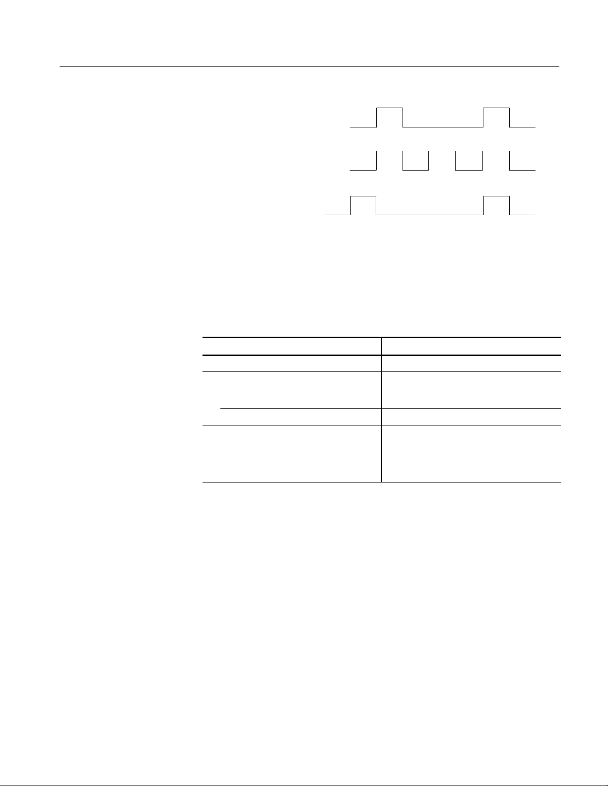
Probe Compensation
Due to variations in oscilloscope input characteristics, you may need to adjust
the low-frequency compensation of the probe when you move it from one
oscilloscope to another. If a 1 kHz calibrated square wave displayed at
1 ms/division shows significant differences between the leading and trailing
edges, perform the following steps to optimize low-frequency compensation:
1. Connect the probe to the calibration signal on the oscilloscope front panel.
2. Press AUTOSET or otherwise adjust your oscilloscope to display a
meaningful waveform.
3. Adjust the trimmer in the probe (accessible through the compensation box)
until you see a square wave with perfectly flat top on the display. See
Figure 3 on page 3.
WARNING. To avoid damaging the trimmer, use the Philips head adjustment tool
supplied with your P5050 probe. Adjustment tools from some probe models may
not be compatible with the P5050 probe. See Figure 2 below.
P5050
Philips
adjust
tool
0.07”
Use
Other
probe
adjust
tools
0.10”
Do not use
Figure 2: Adjusting the trimmer with the P5050 Philips head adjustment tool
2
P5050 Instructions
Page 9

Ground Lead Length
Operating Basics
Undercompensated Overcompensated Properly compensated
Figure 3: Probe compensation waveforms
When you are probing a circuit, you should always use as short a ground lead as
possible between the probe head and circuit ground.
The series inductance added by the probe tip and ground lead can result in a
resonant circuit; this circuit may cause parasitic ringing within the bandwidth of
your oscilloscope. Refer to Figure 4.
Low-inductance
Ground
Figure 4: Waveform distortion from ground lead length
Maximum Working Voltage
Observe Maximum Working Voltage. Do not use the P5050 probe above
300 V
WARNING. To avoid electric shock when using the probe, do not touch the
metallic portions of the probe head while connected to a voltage source.
Three-inch
Ground
CAT II. Refer to the operating chart in Figure 5 on page 7.
RMS
P5050 Instructions
3
Page 10

Operating Basics
Cleaning
To remove accumulated dirt from the probe exterior, use a soft cloth dampened
with a mild detergent and water solution, or use isopropyl alcohol. Do not use
solvents such as benzene, toluene, xylene, or acetone. Avoid abrasive cleaners.
4
P5050 Instructions
Page 11

Features and Accessories
Table 1 illustrates the features and standard accessories of the P5050 probe.
Table 1: Features and Accessories
Feature/Accessory Description Applications/Notes
Guard This feature keeps fingers away from the probe tip for
protection against electric shock.
Guard
Retractable hook tip Connects the probe tip to wires and component leads for
hands-free measurement.
NOTE. For a solid connection, firmly push and twist the hook
tip onto the probe tip before using.
Adjustment tool This Philips head tool is used to adjust probe compensation.
Access the adjustment through the opening in the compensation box.
CAUTION. To avoid damage to the trimmer, use only this
adjustment tool for adjusting probe compensation.
Color marker bands Color codes the probe to the oscilloscope input when more
than one probe is in use. Clip one band around the strain relief
of the probe head and the matching band on the strain relief of
probe output.
SMT KlipChip and ground
lead
Low-inductance ground The ground collar and short lead connect the probe ground to a
Ground lead with insulated
alligator clip
Connects the probe ground to small or hard to reach ground
reference points. Refer to Figure 4 on page 3 for ground lead
length guidelines.
ground reference close to the signal source. The short lead
minimizes aberrations on high-frequency signals caused by the
inductance of the ground lead. Refer to Figure 4 on page 3 for
ground lead length guidelines.
Connects the probe ground to ground reference. Refer to
Figure 4 on page 3 for length guidelines for the ground lead.
NOTE. To remove the ground l ead from the probe, first
unscrew the collar, and then gently pull off the ground lead.
WARNING. T o avoid electric shock when using the probe, keep fingers behind the
guard on the probe body.
P5050 Instructions
5
Page 12

Specifications
The characteristics listed in Table 2 apply to a P5050 probe installed on a
Tektronix TDS5000 Series oscilloscope unless otherwise noted.
Specifications apply when the instrument warms up for a period of at least
20 minutes in an environment that does not exceed the limits described in
Table 3 on page 7.
Table 2: Electrical characteristics
Characteristic Description
Attenuation1(System) 10X ± 0.5% at DC
Input Resistance1(System) 10 MΩ ± 0.5% at DC
Input Capacitance 11.1 pF ± 0.3 pF at probe tip (at 1 KHz,
1 V p-p)
Compensation Range 16 pF to 22 pF
Rise Time, Typical 0.8 nsec, 10% to 90% with TDS5000 series,
≥ 50 mV / div
System Bandwidth (--3 dB) DC to 500 MHz with TDS5000 series
Propagation Delay (Probe), Typical 5.5 ns
Probe Coding 10X
Maximum Input Voltage
1
System characteristic.
2
As defined in EN61010-1. See Certifications and compliances in Table 4 on page 9.
3
RMS=Root Mean Square=rms=The square root of the average of the sum of the
squares of the instantaneous voltage in one cycle = .
300 VDC=300V RMS, 420 V Peak (sinewave)=300 V RMS. See Figure 5 on page 7.
2,3
400 V RMS CAT I or 400 V DC CAT I
300 V RMS CAT II or 300 V DC CAT II
150 V RMS CAT III or 150 V DC CAT III
565 V peak, <50% DF, <1 sec PW
895 V peak, <20% DF, <1 sec PW
1250 V peak, <10% DF, <50 sec PW
See Figure 7 on page 8 f or voltage derating
curve.
Ꭹ
ᒑ
(fxi)2ፒn
6
P5050 Instructions
Page 13
@25% Duty Factor
=(1/2 Peak V) RMS
@50% Duty Factor
=(1.414 (Peak V)) RMS
Special case of square wave:
=[(V
Peak
@20% Duty Factor
)2(Duty Factor)]
1/2
Specifications
0V
0V
0V
Example: Maximum Input Voltage
=[(895 V Pk)
(.20)]
= 400 V RMS
2
1/2
Figure 5: Maximum input voltage calculation example
Table 3: Physical and environm ental characteristics
Characteristic Description
Net Weight (Including Accessories) <0.24lb(110g)
Temperature Range
Operating
Nonoperating –80_ F to +185_ F (–62_ Cto+85_ C)
Humidity
1
Altitude < 9842.5 feet (< 3000 meters), operating
1
Tektronix standard 062-2847-00, class 3. Refer to MIL-E-16400F, paragraph 4.5.9
through 4.5.9.5.1, class 4.
+5_ F to +149_ F
(–15_ Cto+55_ C)
Five cycles (120 hr) at 95% to 97% relative
humidity
< 50,000 feet (< 15,240 meters), nonoperating
P5050 Instructions
7
Page 14

Specifications
10 MΩ
1MΩ
100 KΩ
10 KΩ
Input Impedance
Input Impedance Magnitude and Phase vs. Frequency
1KΩ
100 Ω
100 Hz
1kHz
10 kHz
100 kHz
Frequency
Figure 6: Typical P5050 input impedance
0
-- 1 0
−20
−30
-- 4 0
−50
−60
−70
−80
Input Impedance (phase in deg.)
−90
−100
1MHz
10 MHz
1GHz
100 MHz
10 GHz
Typical P5050 Voltage Derating
350
300
250
200
150
Voltage (RMS)
100
50
0
10 kHz
100 kHz
1MHz
Frequency
Figure 7: Typical P5050 voltage derating curve
10 MHz
100 MHz
8
P5050 Instructions
Page 15

Table 4: Certifications and compliances
Specifications
EC Declaration of
Conformity
Overvoltage
Category
Pollution Degree 2
Safety
Compliance was demonstrated to the following specification as listed in
the Official Journal of the European Communities:
Low Voltage Directive 73/23/EEC as amended by 93/68/EEC:
EN 61010-1/A2
EN 61010-2-031:1994
Category: Examples of Products in this Category:
CAT III Distribution-level mains, fixed installation
CAT II
CAT I
Do not operate in environments where conductive pollutants may be
present.
UL3111-1, First Edition & UL3111-2-031, First Edition
CSA C22.2 No. 1010.1-92 & CAN/CSA C22.2 No. 1010.2.031-94
EN61010-1/A2
EN61010-2-031
Pollution Degree 2
Safety requirements for electrical equipment
for measurement, control, and laboratory use
Particular requirements for hand-held probe
assemblies for electrical measurement and
test
Local-level mains, appliances, portable
equipment
Signal levels in special equipment or parts of
equipment, telecommunications, electronics
P5050 Instructions
9
Page 16

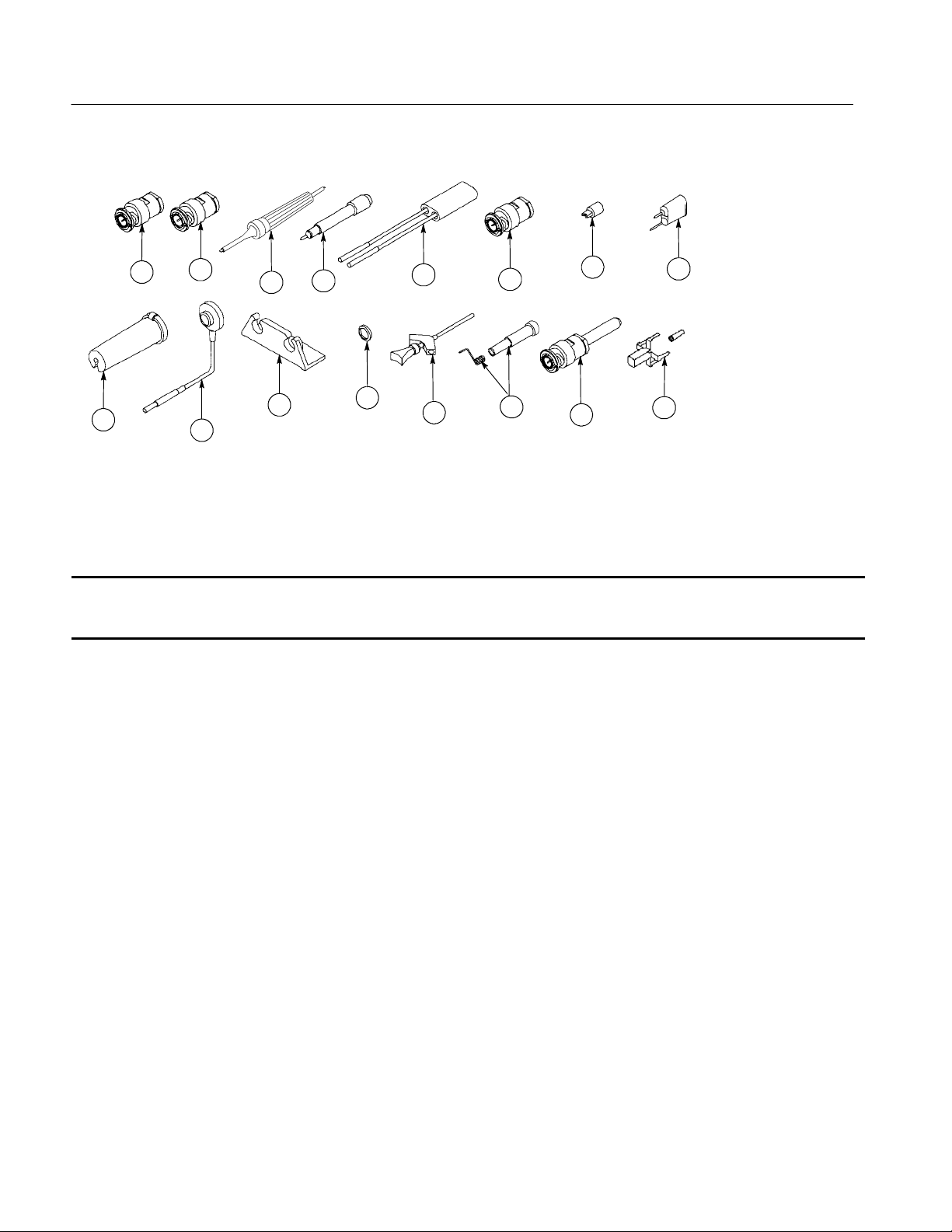
Replaceable Parts
6
2
3
Figure 8: P5050 probe with standard accessories
5
4
11
1
P5050 Replacement
12
13
9
7
8
10
10
P5050 Instructions
Page 17

Replaceable Parts
Replaceable parts: P5050 probe and standard accessories
Fig. &
index
number
8 --1 P5050 1 P5050 10X PASSIVE PROBE, REPLACEMENT
--2 131-3219-00 1 CONN,RF PLUG:BNC, MALE 24931 28P266--3
--3 013--0107--07 1 TIP,PROBE:MINIATURE/COMPACT SIZE,
--4 204--1049--00 1 BODY SHELL:TIP COVER TK2565 204--1049--00
--5 206--0378--00 1 PROBE TIP ASSY:10X,8.0PF,10M OHM 80009 206--0441--00
--6 196--3305--00 1 LEAD,ELECTRICAL:22 AWG,6.0 L,W/CLIP TK2469 196--3305--00
--7 195--4240--00 1 LEAD,ELECTRICAL:0.025 DIA,COPPER,2.3 L TK2469 195--4240--00
--8 016--0633--00 1 MARKER SET,CA:2 EA VARIOUS COLORS 80009 016--0633--00
--9 343--1003--01 1 COLLAR,GND:P5050 TK2565 343--1003--01
--10 196--3113--02 1 LEAD,ELECTRICAL:STRD,22 AWG,6.0 L,8--N TK2469 196--3113--02
--11 003--1433--02 1 SCREWDRIVER:ADJUSTMENT TOOL TK2565 003--1433--02
--12 206--0364--00 1 TIP,PROBE:MICROCKT TEST,0.05 CTR 80009 206--0364--00
--13 -- -- -- -- ------ -- -- -- 1 POUCH,ACCESSORY
Tektronix part
number
071--1018--XX 1 MANUAL,TECH:INSTRUCTIONS,P5050 TK2548 071-- 1018-- XX
Serial no.
effective
Serial no.
discont’d
Qty Name & description
STANDARD ACCESSORIES
RETRACTABLE HOOK ASSY
Mfr.
code
80009 013--0107--07
Mfr. part number
P5050 Instructions
11
Page 18
Replaceable Parts
7
15
10
2
3
11
4
12
5
13
6
14
1
9
8
16
Figure 9: P5050 probe optional accessories
Replaceable parts: P5050 probe optional accessories
Fig. &
index
number
9 --1 013--0226--00 1 CONNECTOR,BNC:BNC TO PROBE TIP ADAPTER 24931 28P264--2
--2 013--0227--00 1 CONNECTOR,BNC:50 OHM,BNC TO P TIP ADAPTER 24931 28P312--1
--3 003--1433--02 1 SCREWDRIVER:ADJUSTMENT TOOL 80009 003--1433--02
--4 013--0202--03 1 ADAPTER,PROBE:SUBMINIATURE/COMPACT TO MIN TK2565 013--0202-- 03
--5 015--0325--01 1 ADAPTER,PROBE:PROBE TO CONNECTOR PINS TK2565 015--0325--01
--6 013--0084--04 1 ADAPTER,CONN:BNC TO PROBE 80009 013--0084--04
--7 015--0201--07 1 TIP,PROBE:IC TEST,PKG OF 10 80009 015-- 0201-- 07
--8 013--0085--00 1 TIP,PROBE:GROUNDING 80009 013--0085--00
--9 352--0670--00 1 HOLDER,PROBE:ATTENUATOR TIPS (3) TK2565 352--0670--00
--10 196--3113--03 1 LEAD,ELECTRICAL:STRD,22 AWG,3.0 L,8-- N TK2469 196--3113--03
--11 352--0351--00 1 HOLDER,PROBE:BLACK ABS P6000 SERIES 7X318 1127
--12 016--0633--00 1 MARKER SET,CA:2 EA VARIOUS COLORS 80009 016--0633--00
--13 SMG50 1 SMT KLIPCHIP:20 ADAPTERS 80009 SMG--50
--14 016--1077--00 1 ACCESSORY KIT:GND TIP CONTACT,PKG OF 2 EA O F 5
--15 013--0254--00 9307 1 ADAPTER,CONN: BNC TO PROBE TIP,MALE 24931 28P--302-- 2
--16 131--5031--00 8926 1 CONNECTOR,PR OBE:PKG OF 25,COMPACT 8009 131--5031--00
Tektronix part
number
015--0201--08 1 TIP,PROBE:IC TEST,PKG OF 100 80009 015--0201--08
Serial no.
effective
Serial no.
discont’d
Qty Name & description
OPTIONAL ACCESSORIES
NOTE: ITEMS 5 THROUGH 9 ARE USABLE WHEN THE
SUBMINIATURE/COMPACT TO MINIATURE PROBE TIP
ADAPTER IS USED. (ITEM 4)
LENGTHS W/COVER SHELL
Mfr.
code
80009 016--1077--00
Mfr. part number
12
P5050 Instructions
Page 19

Manufacturers cr oss index
Mfr.
code
24931 BERG ELECTRONICS INC BERG ELECTRONICS RF/COAXIAL DIV
7X318 KASO PLASTICS INC 11013 A N E 39TH VANCOUVER, WA 98662
80009 TEKTRONIX INC 14150 SW KARL BRAUN DR
TK2469 TENSOLITE CORPORATION 3000 LEWIS & CLARK HWY
TK2548 XEROX CORPORATION 14181 SW MILLIKAN WAY BEAVERTON, OR 97005
TK2565 VISION PLASTICS INC 26000 SW PARKWAY CENTER DRIVE WILSONVILLE, OR 97070
Manufacturer Address City, state, zip code
FRANKLIN, IN 46131
2100 EARLYWOOD DR
PO BOX 547
BEAVERTON, OR 97077-- 0001
PO BOX 500
VANCOUVER, WA 98661
SUITE 2
Replaceable Parts
P5050 Instructions
13
Page 20

Replaceable Parts
14
P5050 Instructions
 Loading...