

Page 1

5 Series MSO
MSO54, MSO56, MSO58, MSO58LP
Specifications and Performance Verification
Warning: The servicing instructions are for use by qualified personnel only. To avoid personal injury, do not perform any servicing unless you are qualified
to do so. Refer to all safety summaries prior to performing service.
Supports product Firmware V1.4 and above. Revision B; released February 10, 2020.
Register now!
Click the following link to protect your product.
www.tek.com/register
077-1306-06
Page 2

Copyright © Tektronix. All rights reserved. Licensed software products are owned by Tektronix or its subsidiaries or suppliers, and are
protected by national copyright laws and international treaty provisions. Tektronix products are covered by U.S. and foreign patents, issued
and pending. Information in this publication supersedes that in all previously published material. Specifications and price change privileges
reserved.
TEKTRONIX and TEK are registered trademarks of Tektronix, Inc.
FlexChannel, e*Scope, and TekVPI are registered trademarks of Tektronix, Inc.
5 Series MSO Specifications and Verification manual. Released 20180621
Contacting Tektronix
Tektronix, Inc.
14150 SW Karl Braun Drive
P.O. Box 500
Beaverton, OR 97077
USA
For product information, sales, service, and technical support:
• In North America, call 1-800-833-9200.
• Worldwide, visit www.tek.com to find contacts in your area.
Page 3

Table of Contents
Table of Contents
List of Figures................................................................................................................................................................................5
List of Tables................................................................................................................................................................................. 6
Important safety information..........................................................................................................................................................7
General safety summary........................................................................................................................................................7
Terms in the manual...............................................................................................................................................................8
Terms on the product............................................................................................................................................................. 9
Symbols on the product......................................................................................................................................................... 9
Specifications.............................................................................................................................................................................. 10
Analog channel input and vertical specification................................................................................................................... 10
Timebase system.................................................................................................................................................................19
Trigger system..................................................................................................................................................................... 21
Serial Trigger specifications.................................................................................................................................................25
Digital acquisition system.....................................................................................................................................................27
Digital volt meter (DVM).......................................................................................................................................................27
Trigger frequency counter....................................................................................................................................................28
Arbitrary Function Generator system................................................................................................................................... 28
Display system (MSO54, MSO56, MSO58).........................................................................................................................30
Processor system................................................................................................................................................................ 31
Input/Output port specifications........................................................................................................................................... 31
Data storage specifications..................................................................................................................................................32
Power supply system........................................................................................................................................................... 34
Safety characteristics...........................................................................................................................................................34
Environmental specifications............................................................................................................................................... 34
Mechanical specifications.................................................................................................................................................... 35
Performance verification procedures.......................................................................................................................................... 36
Test records......................................................................................................................................................................... 36
Instrument information, self test record.........................................................................................................................36
Input Impedance test record......................................................................................................................................... 37
DC Balance test record.................................................................................................................................................38
DC Gain Accuracy test record...................................................................................................................................... 44
DC Offset Accuracy test record.................................................................................................................................... 55
Analog Bandwidth test record.......................................................................................................................................58
Random Noise, sample acquisition mode test record...................................................................................................93
Random Noise, High Res mode test record................................................................................................................116
Long term sample rate through AFG DC offset accuracy test records....................................................................... 139
Performance tests..............................................................................................................................................................163
Prerequisites...................................................................................................................................................................... 163
Self test.............................................................................................................................................................................. 164
Check input impedance..................................................................................................................................................... 164
Check DC balance............................................................................................................................................................. 165
Check DC gain accuracy................................................................................................................................................... 167
Check DC offset accuracy..................................................................................................................................................169
Check analog bandwidth....................................................................................................................................................170
Check random noise, sample acquisition mode ............................................................................................................... 173
5 Series MSO MSO54, MSO56, MSO58, MSO58LP Specifications and Performance Verification 3
Page 4

Table of Contents
Check random noise, High Res mode............................................................................................................................... 175
Check long term sample rate............................................................................................................................................. 176
Check delta time measurement accuracy..........................................................................................................................177
Check digital threshold accuracy....................................................................................................................................... 179
Check AUX Out output voltage levels................................................................................................................................180
Check DVM voltage accuracy (DC)................................................................................................................................... 182
Check DVM voltage accuracy (AC)................................................................................................................................... 183
Check trigger frequency accuracy and maximum input frequency.................................................................................... 183
Arbitrary function generator............................................................................................................................................... 184
Check AFG sine and ramp frequency accuracy......................................................................................................... 184
Check AFG square and pulse frequency accuracy.....................................................................................................185
Check AFG signal amplitude accuracy.......................................................................................................................186
Check AFG DC offset accuracy..................................................................................................................................187
Index......................................................................................................................................................................................... 190
5 Series MSO MSO54, MSO56, MSO58, MSO58LP Specifications and Performance Verification 4
Page 5

List of Figures
List of Figures
Figure 1: Frequency/period test................................................................................................................................................ 184
Figure 2: Frequency/period test................................................................................................................................................ 185
Figure 3: 50 Ω terminator accuracy...........................................................................................................................................186
Figure 4: Amplitude test............................................................................................................................................................ 187
Figure 5: 50 Ω terminator accuracy...........................................................................................................................................188
Figure 6: DC offset tests............................................................................................................................................................188
5 Series MSO MSO54, MSO56, MSO58, MSO58LP Specifications and Performance Verification 5
Page 6

List of Tables
List of Tables
Table 1: 5 Series MSO ............................................................................................................................................................... 21
Table 2: MSO58LP .....................................................................................................................................................................21
Table 3: Expected gain worksheet............................................................................................................................................ 168
Table 4: Maximum bandwidth frequency worksheet................................................................................................................. 172
Table 5: CF (Calibration Factor) = 1.414 × ((50 / Measurement Ω) + 1)...................................................................................186
Table 6: CF (Calibration Factor) = 0.5 × (( 50 / Measurement Ω) + 1)......................................................................................188
5 Series MSO MSO54, MSO56, MSO58, MSO58LP Specifications and Performance Verification 6
Page 7

Important safety information
Important safety information
This manual contains information and warnings that must be followed by the user for safe operation and to keep the product in a safe
condition.
General safety summary
Use the product only as specified. Review the following safety precautions to avoid injury and prevent damage to this product or any
products connected to it. Carefully read all instructions. Retain these instructions for future reference.
This product shall be used in accordance with local and national codes.
For correct and safe operation of the product, it is essential that you follow generally accepted safety procedures in addition to the safety
precautions specified in this manual.
The product is designed to be used by trained personnel only.
Only qualified personnel who are aware of the hazards involved should remove the cover for repair, maintenance, or adjustment.
Before use, always check the product with a known source to be sure it is operating correctly.
This product is not intended for detection of hazardous voltages.
Use personal protective equipment to prevent shock and arc blast injury where hazardous live conductors are exposed.
To avoid fire or personal injury
Use proper power cord Use only the power cord specified for this product and certified for the country of use. Do not use the
provided power cord for other products.
Ground the product This product is grounded through the grounding conductor of the power cord. To avoid electric shock, the
grounding conductor must be connected to earth ground. Before making connections to the input or output
terminals of the product, ensure that the product is properly grounded. Do not disable the power cord
grounding connection.
Power disconnect The power cord disconnects the product from the power source. See instructions for the location. Do not
position the equipment so that it is difficult to operate the power cord; it must remain accessible to the user
at all times to allow for quick disconnection if needed.
Connect and disconnect
properly
Observe all terminal ratings To avoid fire or shock hazard, observe all rating and markings on the product. Consult the product manual
Do not operate without covers Do not operate this product with covers or panels removed, or with the case open. Hazardous voltage
Avoid exposed circuitry Do not touch exposed connections and components when power is present.
Do not operate with suspected
failures
Do not connect or disconnect probes or test leads while they are connected to a voltage source.
Use only insulated voltage probes, test leads, and adapters supplied with the product, or indicated by
Tektronix to be suitable for the product.
for further ratings information before making connections to the product. Do not exceed the Measurement
Category (CAT) rating and voltage or current rating of the lowest rated individual component of a product,
probe, or accessory. Use caution when using 1:1 test leads because the probe tip voltage is directly
transmitted to the product.
Do not apply a potential to any terminal, including the common terminal, that exceeds the maximum rating
of that terminal.
exposure is possible.
If you suspect that there is damage to this product, have it inspected by qualified service personnel.
5 Series MSO MSO54, MSO56, MSO58, MSO58LP Specifications and Performance Verification 7
Page 8

Important safety information
Disable the product if it is damaged. Do not use the product if it is damaged or operates incorrectly. If in
doubt about safety of the product, turn it off and disconnect the power cord. Clearly mark the product to
prevent its further operation.
Before use, inspect voltage probes, test leads, and accessories for mechanical damage and replace when
damaged. Do not use probes or test leads if they are damaged, if there is exposed metal, or if a wear
indicator shows.
Examine the exterior of the product before you use it. Look for cracks or missing pieces.
Use only specified replacement parts.
Do not operate in wet/damp
conditions
Do not operate in an explosive
atmosphere
Keep product surfaces clean
and dry
Provide proper ventilation Refer to the installation instructions in the manual for details on installing the product so it has proper
Provide a safe working
environment
Be aware that condensation may occur if a unit is moved from a cold to a warm environment.
Remove the input signals before you clean the product.
ventilation.
Slots and openings are provided for ventilation and should never be covered or otherwise obstructed. Do
not push objects into any of the openings.
Always place the product in a location convenient for viewing the display and indicators.
Avoid improper or prolonged use of keyboards, pointers, and button pads. Improper or prolonged keyboard
or pointer use may result in serious injury.
Be sure your work area meets applicable ergonomic standards. Consult with an ergonomics professional to
avoid stress injuries.
Use care when lifting and carrying the product. This product is provided with a handle or handles for lifting
and carrying.
Warning: The product is heavy. To reduce the risk of personal injury or damage to the device get
help when lifting or carrying the product.
Use only the Tektronix rackmount hardware specified for this product.
Probes and test leads
Before connecting probes or test leads, connect the power cord from the power connector to a properly grounded power outlet.
Keep fingers behind the protective barrier, protective finger guard, or tactile indicator on the probes.
Remove all probes, test leads and accessories that are not in use.
Use only correct Measurement Category (CAT), voltage, temperature, altitude, and amperage rated probes, test leads, and adapters for
any measurement.
Terms in the manual
These terms may appear in this manual:
Warning:
CAUTION: Caution statements identify conditions or practices that could result in damage to this product or other property.
Warning statements identify conditions or practices that could result in injury or loss of life.
5 Series MSO MSO54, MSO56, MSO58, MSO58LP Specifications and Performance Verification 8
Page 9
Terms on the product
These terms may appear on the product:
• DANGER indicates an injury hazard immediately accessible as you read the marking.
• WARNING indicates an injury hazard not immediately accessible as you read the marking.
• CAUTION indicates a hazard to property including the product.
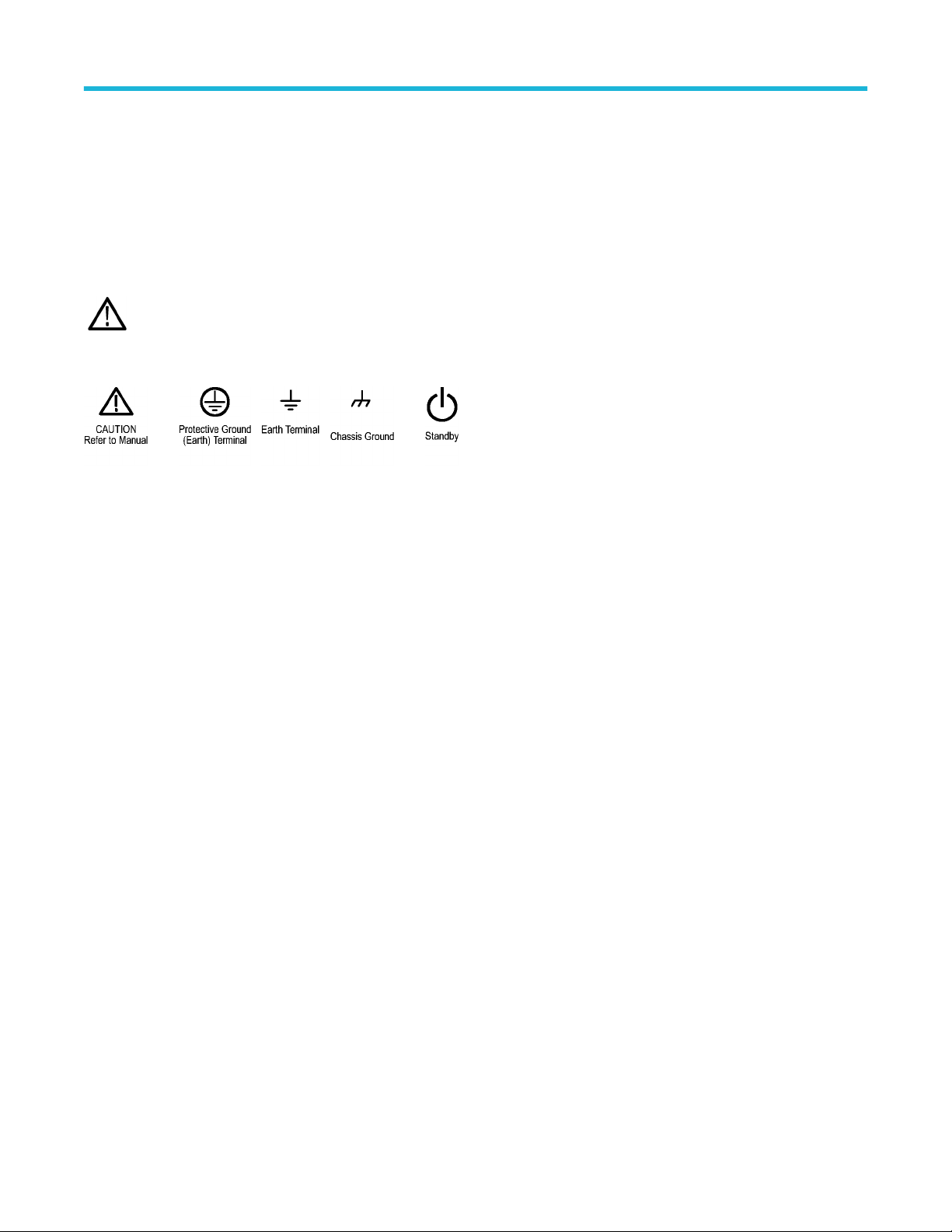
Symbols on the product
When this symbol is marked on the product, be sure to consult the manual to find out the nature of the potential hazards and
any actions which have to be taken to avoid them. (This symbol may also be used to refer the user to ratings in the manual.)
The following symbols may appear on the product:
Important safety information
5 Series MSO MSO54, MSO56, MSO58, MSO58LP Specifications and Performance Verification 9
Page 10

Specifications
Specifications
This chapter contains specifications for the instrument. All specifications are guaranteed unless noted as "typical." Typical specifications
are provided for your convenience but are not guaranteed. Specifications that are marked with the symbol are checked in this manual.
All specifications apply to all models unless noted otherwise.
To meet specifications, these conditions must first be met:
• The instrument must have been calibrated in an ambient temperature between 18 °C and 28 °C (64 °F and 82 °F).
• The instrument must be operating within the environmental limits. (See Environmental specifications on page 34.)
• The instrument must be powered from a source that meets the specifications. (See Power supply system on page 34.)
• The instrument must have been operating continuously for at least 20 minutes within the specified operating temperature range.
• You must perform the Signal Path Compensation procedure after the warmup period. See the online help for instructions on how to
perform signal path compensation. If the ambient temperature changes more than 5 °C (9 °F) , repeat the procedure.
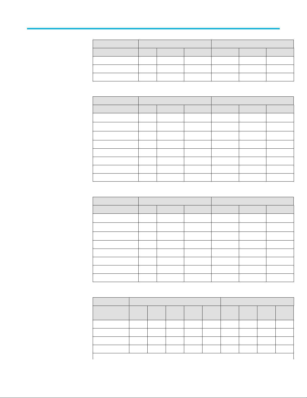
Analog channel input and vertical specification
Number of input channels MSO54: 4 BNC
MSO56: 6 BNC
MSO58: 8 BNC
MSO58LP: 8 BNC
Input coupling DC, AC
Input resistance selection 1 MΩ or 50 Ω
✓Input impedance 1 MΩ DC
coupled
Input capacitance 1 MΩ DC
coupled, typical
✓Input impedance 50 Ω, DC
coupled
Maximum input voltage, 1 MΩ 300 V
Maximum input voltage, 50
Ohm
1 MΩ ±1%
14.5 pF ±1.5 pF, 2 GHz model
13 pF ±1.5 pF, 1 GHz, 500 MHz, 350 MHz models
14 pF ±1.5 pF, MSO58LP
50 Ω ±1% (VSWR ≤1.5:1, typical)
at the BNC. Installation Category II
RMS
Derate at 20 dB/decade between 4.5 MHz and 45 MHz; derate 14 dB/decade between 45 MHz and 450
MHz. Above 450 MHz, 5.5 V
Maximum peak input voltage at the BNC: ±425 V
5 V
, with peaks ≤ ±20 V (DF ≤6.25%)
RMS
RMS
DC balance ✓ 0.1 div with DC-50 Ω oscilloscope input impedance (50 Ω BNC terminated)
✓ 0.2 div at 1 mV/div with DC-50 Ω oscilloscope input impedance (50 Ω BNC terminated)
0.4 div at 500 μV/div with DC-50 Ω oscilloscope input impedance (50 Ω BNC terminated)
✓ 0.2 div with DC-1 MΩ oscilloscope input impedance (50 Ω BNC terminated)
5 Series MSO MSO54, MSO56, MSO58, MSO58LP Specifications and Performance Verification 10
Page 11

0.4 div at 500 µV/div with DC-1 MΩ scope input impedance (50 Ω BNC terminated)
Note: 500 µV/div is a 2X digital zoom of 1 mV/div. As such, it is guaranteed by testing the 1 mV/div setting.
Number of digitized bits 8 bits at 6.25 GS/s
12 bits at 3.125 GS/s
13 bits at 1.25 GS/s
14 bits at 625 MS/s
15 bits at 312.5 MS/s
16 bits at 125 MS/s
Displayed vertically with 25 digitization levels (DL 1) per division, (8-bits only) 10.24 divisions dynamic
range.
Sensitivity range, coarse
1 MΩ 500 µV/div to 10 V/div in a 1-2-5 sequence
50 Ω 500 µV/div to 1 V/div in a 1-2-5 sequence
Note: 500 μV/div is a 2X digital zoom of 1 mV/div
Specifications
Sensitivity range, fine
Allows continuous adjustment from 1 mV/div to 10 V/div, 1 MΩ and from 1 mV/div to 1 V/div, 50 Ω
1 MΩ 500 µV/div to 10 V/div
50 Ω 500 µV/div to 1 V/div
Sensitivity resolution, fine ≤1% of current setting
DC gain accuracy
✓ DC gain accuracy
2 GHz model, Step Gain, 50
Ohm
2 GHz model, Step Gain, 1
Meg Ohm
1 GHz, 500 MHz, 350 MHz
models, MSO58LP, Step
Gain
Variable gain ±1.5%, derated at 0.100%/ °C above 30 °C.
Note: 500 µV/div is a 2X digital zoom of 1 mV/div. As such, it is guaranteed by testing the 1 mV/div setting.
Offset ranges, maximum
±1.2%, (±2.0% at 1 mV/div and 500 µV/div settings), de-rated at 0.100%/ °C above 30 °C
±1.0%, (±2.0% at 1 mV/div and 500 µV/div settings), de-rated at 0.100%/ °C above 30 °C
±1.0%, (±2.0% at 1 mV/div and 500 µV/div settings), de-rated at 0.100%/ °C above 30 °C
2 GHz models Input signal cannot exceed maximum input voltage for the 50 Ω input path.
1
DL is the abbreviation for digitization level. A DL is the smallest voltage level change that can be resolved by an 8-bit A-D Converter. This value is also known as an
LSB (least significant bit).
5 Series MSO MSO54, MSO56, MSO58, MSO58LP Specifications and Performance Verification 11
Page 12
Volts/div Setting Maximum offset range, 50 Ω Input
500 µV/div - 50 mV/div ±1 V
51 mV/div - 99 mV/div ± (-10 * (Volts/div Setting) + 1.5 V)
100 mV/div - 500 mV/div ±10 V
501 mV/div - 1 V/div ± (-10 * (Volts/div Setting) + 15 V)
Volts/div Setting Maximum offset range, 1 MΩ Input
500 µV/div - 63 mV/div ±1 V
64 mV/div - 999 mV/div ±10 V
1 V/div - 10 V/div ±100 V
Specifications
≤ 1 GHz models (including
MSO58LP)
Note: 500 µV/div is a 2X digital zoom of 1 mV/div. As such, it is guaranteed by testing the 1 mV/div setting.
Position range ±5 divisions
Offset accuracy ±(0.005 X | offset - position | + DC balance )
Number of waveforms for
average acquisition mode
DC voltage measurement
accuracy, Average acquisition
mode
Input signal cannot exceed maximum input voltage for the 50 Ω input path.
Volts/div Setting Maximum offset range
50 Ω Input 1 MΩ Input
500 µV/div - 63 mV/div ±1 V ±1 V
64 mV/div - 999 mV/div ±10 V ±10 V
1 V/div - 10 V/div ±10 V ±100 V
2 to 10,240 Waveforms, default 16 waveforms
Measurement Type DC Accuracy (In Volts)
Average of ≥ 16 waveforms ±((DC Gain Accuracy) * |reading - (offset - position)|
Delta volts between any two averages of ≥ 16
waveforms acquired with the same oscilloscope
setup and ambient conditions
+ Offset Accuracy + 0.1 * V/div setting)
±(DC Gain Accuracy * |reading| + 0.05 div)
DC voltage measurement
accuracy, sample acquisition
mode, typical
Bandwidth selections 20 MHz, 250 MHz, and the full bandwidth value of your model
Bandwidth selections 20 MHz, 250 MHz, and 1 GHz
✓Analog bandwidth 50 Ω DC coupled
5 Series MSO MSO54, MSO56, MSO58, MSO58LP Specifications and Performance Verification 12
Measurement Type DC Accuracy (In Volts)
Any Sample ±(DC Gain Accuracy * |reading - (offset - position)| +
Offset Accuracy + 0.15 div + 0.6 mV)
Delta Volts between any two samples acquired with
the same scope setup and ambient conditions
±(DC Gain Accuracy * |reading| + 0.15 div + 1.2
mV)
Page 13
Specifications
2 GHz models
1 GHz models
500 MHz models
350 MHz models
Volts/Div Setting Bandwidth
10 mV/div - 1 V/div DC - 2.00 GHz
5 mV/div - 9.98 mV/div DC - 1.50 GHz
2 mV/div - 4.98 mV/div DC - 350 MHz
1 mV/div - 1.99 mV/div DC - 175 MHz
500 µV/div - 995 µV/div DC - 175 MHz
Volts/Div Setting Bandwidth
1 mV/div - 1 V/div DC - 1.00 GHz
500 µV/div - 995 µV/div DC - 250 MHz
Volts/Div Setting Bandwidth
1 mV/div - 1 V/div DC - 500 MHz
500 µV/div - 995 µV/div DC - 250 MHz
Volts/Div Setting Bandwidth
1 mV/div - 1 V/div DC - 350 MHz
500 µV/div - 995 µV/div DC - 250 MHz
Analog bandwidth, 1 MΩ, typical
All model bandwidths
except 350 MHz
350 MHz models
Analog bandwidth with
TPP0500, TPP1000 probes,
typical
Lower frequency limit, AC
coupled, typical
Volts/Div Setting Bandwidth
1 mV/div - 10 V/div DC - 500 MHz
500 µV/div - 995 µV/div DC - 250 MHz
Volts/Div Setting Bandwidth
1 mV/div - 10 V/div DC - 350 MHz
500 µV/div - 995 µV/div DC - 250 MHz
The limits are for ambient temperature of ≤30 °C and the bandwidth selection set to FULL. Reduce the
upper bandwidth frequency by 1% for each °C above 30 °C.
Instrument Volts/Div Setting Bandwidth
2 GHz, 1 GHz 5 mV/div - 100 V/div DC - 1 GHz (TPP1000 Probe)
500 MHz 5 mV/div - 100 V/div DC - 500 MHz (TPP0500 Probe)
350 MHz 5 mV/div - 100 V/div DC - 350 MHz (TPP0500 Probe)
<10 Hz when AC 1 MΩ coupled. The AC coupled lower frequency limits are reduced by a factor of 10 (<1
Hz) when 10X passive probes are used.
Upper frequency limit, 250 MHz
bandwidth limited, typical
5 Series MSO MSO54, MSO56, MSO58, MSO58LP Specifications and Performance Verification 13
250 MHz, ± 25%
Page 14

Specifications
Upper frequency limit, 20 MHz
bandwidth limited, typical
20 MHz, ± 20%
Calculated rise time
Calculated rise time, typical
Peak Detect or Envelope mode
pulse response, typical
Effective bits (ENOB), typical
Typical effective bits for a 9-division p-p sine-wave input, 50 mV/div, 50-ohm
2 GHz models, Sample
mode, 50 Ω
Model 50 Ω TPP0500 Probe TP1000 Probe
Vertical 500 µV-1 V 5 mV-10 V 5 mV-10 V
2 GHz 225 ps 800 ps 400 ps
1 GHz 400 ps 800 ps 400 ps
500 MHz 800 ps 800 ps 800 ps
350 MHz 1.15 ns 1.15 ns 1.15 ns
Minimum pulse width is >640 ps (6.25 GS/s)
Bandwidth Input frequency 6.25 GS/s
2 GHz 10 MHz 6.20
2 GHz 600 MHz 6.20
250 MHz 10 MHz 7.30
250 MHz 200 MHz 7.30
20 MHz 10 MHz 7.60
2 GHz models, High Res
mode, 50 Ω
1 GHz, 500 MHz, 350 MHz
models, Sample mode, 50
Ω
Bandwidth Input frequency 6.25 GS/s
1 GHz 10 MHz 7.00
1 GHz 300 MHz 7.00
250 MHz 10 MHz 7.80
250 MHz 100 MHz 7.80
20 MHz 10 MHz 8.70
Bandwidth Input Frequency 6.25 GS/s
1 GHz 10 MHz 7.10
1 GHz 300 MHz 7.10
500 MHz 10 MHz 7.40
500 MHz 150 MHz 7.40
350 MHz 10 MHz 7.60
350 MHz 100 MHz 7.60
250 MHz 10 MHz 7.50
250 MHz 100 MHz 7.50
20 MHz 10 MHz 7.70
5 Series MSO MSO54, MSO56, MSO58, MSO58LP Specifications and Performance Verification 14
Page 15
Specifications
1 GHz, 500 MHz, 350 MHz
models, High Res mode, 50
Ω
Bandwidth Input frequency 6.25 GS/s
1 GHz 10 MHz 7.60
1 GHz 300 MHz 7.50
500 MHz 10 MHz 7.90
500 MHz 150 MHz 7.80
350 MHz 10 MHz 8.20
350 MHz 100 MHz 8.20
250 MHz 10 MHz 8.10
250 MHz 100 MHz 8.10
20 MHz 10 MHz 8.90
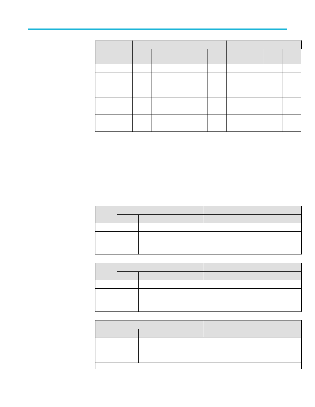
Random noise, sample acquisition mode
✓2 GHz models, Sample
mode (RMS)
2 GHz models 50 Ω 1 MΩ
V/div 2 GHz 250 MHz 20 MHz 500 MHz 250 MHz 20 MHz
1 mV/div
2 mV/div
5 mV/div
10 mV/div 643 μV 244 μV 174 μV 377 μV 271 μV 201 μV
20 mV/div 1.06 mV 436 μV 347 μV 572 μV 462 μV 373 μV
50 mV/div 2.51 mV 1.06 mV 869 μV 1.32 mV 1.11 mV 922 μV
100 mV/div 6.15 mV 2.38 mV 1.74 mV 2.75 mV 2.24 mV 1.88 mV
1 V/div 39.6 mV 21.1 mV 17.4 mV 28.6 mV 23.5 mV 18.7 mV
2
3
4
89.8 μV 89.8 μV 39.6 μV 270 μV 158 μV 85.5 μV
152 μV 114 μV 50.6 μV 291 μV 158 μV 90.1 μV
456 μV 155 μV 88.9 μV 315 μV 185 μV 121 μV
2 GHz models, Sample
mode (RMS), typical
2 GHz models 50 Ω 1 MΩ
V/div 2 GHz 250 MHz 20 MHz 500 MHz 250 MHz 20 MHz
1 mV/div
2 mV/div
5 mV/div
2
3
4
69.4 μV 69.4 μV 30.6 μV 208 μV 122 μV 66 μV
117 μV 88.0 μV 39.1 μV 225 μV 122 μV 69.7 μV
353 μV 120 μV 68.7 μV 243 μV 143 μV 93.8 μV
10 mV/div 497 μV 188 μV 125 μV 291 μV 209 μV 156 μV
20 mV/div 816 μV 337 μV 251 μV 442 μV 357 μV 288 μV
Table continued…
2
Bandwidth at 1 mV/div is limited to 175 MHz in 50 Ω.
3
Bandwidth at 2 mV/div is limited to 350 MHz in 50 Ω.
4
Bandwidth at 5 mV/div is limited to 1.5 GHz in 50 Ω.
5 Series MSO MSO54, MSO56, MSO58, MSO58LP Specifications and Performance Verification 15
Page 16
✓2 GHz models, High Res
mode (RMS)
Specifications
2 GHz models 50 Ω 1 MΩ
V/div 2 GHz 250 MHz 20 MHz 500 MHz 250 MHz 20 MHz
50 mV/div 1.94 mV 822 μV 627 μV 1.02 mV 857 μV 712 μV
100 mV/div 4.75 mV 1.84 mV 1.25 mV 2.13 mV 1.73 mV 1.45 mV
1 V/div 30.6 mV 16.3 mV 12.5 mV 22.1 mV 18.2 mV 14.5 mV
2 GHz models 50 Ω 1 MΩ
V/div 1 GHz 250 MHz 20 MHz 500 MHz 250 MHz 20 MHz
1 mV/div
2 mV/div
5 mV/div
2
3
4
86.5 μV 86.5 μV 35.2 μV 269 μV 152 μV 83.6 μV
125 μV 100 μV 36.9 μV 290 μV 152 μV 86.3 μV
261 μV 140 μV 48.4 μV 308 μV 172 μV 88.9 μV
10 mV/div 356 μV 191 μV 72.6 μV 359 μV 224 μV 108 μV
20 mV/div 607 μV 325 μV 137 μV 538 μV 360 μV 162 μV
50 mV/div 1.43 mV 763 μV 327 μV 1.19 mV 803 μV 351 μV
100 mV/div 3.56 mV 1.91 mV 779 μV 2.45 mV 1.76 mV 780 μV
1 V/div 23.8 mV 14 mV 6.05 mV 26.3 mV 18.9 mV 8.46 mV
2 GHz models, High Res
mode (RMS), typical
✓1 GHz, 500 MHz, 350
MHz models, Sample mode
(RMS)
2 GHz models 50 Ω 1 MΩ
V/div 1 GHz 250 MHz 20 MHz 500 MHz 250 MHz 20 MHz
1 mV/div
2 mV/div
5 mV/div
2
3
4
66.8 μV 66.8 μV 27.2 μV 208 μV 117 μV 64.6 μV
96.9 μV 77.5 μV 28.5 μV 224 μV 117 μV 66.7 μV
202 μV 108 μV 37.4 μV 238 μV 133 μV 68.7 μV
10 mV/div 275 μV 147 μV 56.1 μV 277 μV 173 μV 83.6 μV
20 mV/div 469 μV 251 μV 106 μV 416 μV 278 μV 125 μV
50 mV/div 1.10 mV 589 μV 253 μV 916 μV 620 μV 271 μV
100 mV/div 2.75 mV 1.47 mV 602 μV 1.90 mV 1.36 mV 603 μV
1 V/div 18.4 mV 10.8 mV 4.68 mV 20.3 mV 14.6 mV 6.54 mV
< 2 GHz models 50 Ω 1 MΩ
V/div 1 GHz 500
MHz
350
MHz
250 Mhz 20 MHz 500
MHz
350
MHz
250
MHz
20 MHz
1 mV/div 372 μV 253 μV 181 μV 153 μV 91.4 μV 258 μV 188 μV 158 μV 87.9 μV
2 mV/div 376 μV 262 μV 190 μV 164 μV 102 μV 254 μV 193 μV 158 μV 92.0 μV
5 mV/div 395 μV 292 μV 222 μV 201 μV 136 μV 272 μV 207 μV 185 μV 116 μV
10 mV/div 449 μV 359 μV 284 μV 272 μV 197 μV 319 μV 264 μV 251 μV 188 μV
Table continued…
5 Series MSO MSO54, MSO56, MSO58, MSO58LP Specifications and Performance Verification 16
Page 17

1 GHz, 500 MHz, 350
MHz models, Sample mode
(RMS), typical
Specifications
< 2 GHz models 50 Ω 1 MΩ
V/div 1 GHz 500
MHz
20 mV/div 614 μV 529 μV 436 μV 435 μV 347 μV 455 μV 422 μV 422 μV 347 μV
50 mV/div 1.26 mV 1.14 mV 962 μV 982 μV 869 μV 1.03 mV 898 μV 1.00 mV 869 μV
100 mV/div 2.85 mV 2.50 mV 2.08 mV 2.09 mV 1.74 mV 2.18 mV 1.91 mV 2.06 mV 1.74 mV
1 V/div 24.6 mV 22.4 mV 18.9 mV 19.4 mV 17.4 mV 23.1 mV 21.1 mV 21.6 mV 17.4 mV
< 2 GHz models 50 Ω 1 MΩ
V/div 1 GHz 500
MHz
1 mV/div 287 μV 196 μV 140 μV 118 μV 70.6 μV 199 μV 145 μV 122 μV 67.9 μV
2 mV/div 290 μV 202 μV 147 μV 127 μV 78.9 μV 196 μV 149 μV 122 μV 71.1 μV
5 mV/div 305 μV 226 μV 171 μV 156 μV 105 μV 210 μV 160 μV 143 μV 89.8 μV
10 mV/div 347 μV 277 μV 219 μV 210 μV 153 μV 246 μV 204 μV 194 μV 146 μV
20 mV/div 475 μV 409 μV 337 μV 336 μV 257 μV 352 μV 326 μV 326 μV 251 μV
50 mV/div 977 μV 883 μV 743 μV 758 μV 627 μV 796 μV 694 μV 775 μV 627 μV
100 mV/div 2.20 mV 1.93 mV 1.60 mV 1.61 mV 1.25 mV 1.68 mV 1.48 mV 1.59 mV 1.25 mV
1 V/div 19.0 mV 17.3 mV 14.6 mV 15.0 mV 12.5 mV 17.9 mV 16.3 mV 16.7 mV 12.5 mV
350
MHz
350
MHz
250 Mhz 20 MHz 500
MHz
250
MHz
20 MHz 500
MHz
350
MHz
350
MHz
250
MHz
250
MHz
20 MHz
20 MHz
✓1 GHz, 500 MHz, 350
MHz models, High Res
mode (RMS)
1 GHz, 500 MHz, 350 MHz
models, High Res mode
(RMS), typical
< 2 GHz models 50 Ω 1 MΩ
V/div 1 GHz 500
MHz
1 mV/div 329 μV 256 μV 183 μV 152 μV 90.6 μV 245 μV 184 μV 153 μV 83.8 μV
2 mV/div 330 μV 256 μV 185 μV 157 μV 91.2 μV 251 μV 188 μV 156 μV 85.4 μV
5 mV/div 339 μV 262 μV 195 μV 172 μV 94.3 μV 254 μV 197 μV 169 μV 90.1 μV
10 mV/div 367 μV 282 μV 218 μV 205 μV 103 μV 274 μV 216 μV 200 μV 101 μV
20 mV/div 462 μV 354 μV 287 μV 288 μV 132 μV 348 μV 277 μV 289 μV 135 μV
50 mV/div 876 μV 667 μV 564 μV 595 μV 254 μV 634 μV 530 μV 621 μV 268 μV
100 mV/div 2.09 mV 1.60 mV 1.31 mV 1.34 mV 601 μV 1.51 mV 1.25 mV 1.36 mV 615 μV
1 V/div 16.8 mV 12.8 mV 10.9 mV 11.6 mV 4.88 mV 17.6 mV 13.7 mV 14.4 mV 7.08 mV
350
MHz
250
MHz
20 MHz 500
MHz
350
MHz
250
MHz
20 MHz
5 Series MSO MSO54, MSO56, MSO58, MSO58LP Specifications and Performance Verification 17
Page 18
Specifications
< 2 GHz models 50 Ω 1 MΩ
V/div 1 GHz 500
MHz
1 mV/div 254 μV 198 μV 141 μV 118 μV 70.0 μV 189 μV 143 μV 118 μV 64.8 μV
2 mV/div 255 μV 198 μV 143 μV 121 μV 70.4 μV 194 μV 145 μV 121 μV 66.0 μV
5 mV/div 262 μV 202 μV 150 μV 133 μV 72.8 μV 196 μV 152 μV 130 μV 69.6 μV
10 mV/div 283 μV 218 μV 169 μV 158 μV 79.8 μV 212 μV 167 μV 154 μV 78.2 μV
20 mV/div 357 μV 273 μV 222 μV 223 μV 102 μV 269 μV 214 μV 223 μV 104 μV
50 mV/div 677 μV 516 μV 436 μV 460 μV 196 μV 490 μV 410 μV 480 μV 207 μV
100 mV/div 1.61 mV 1.23 mV 1.02 mV 1.04 mV 464 μV 1.16 mV 964 μV 1.05 mV 475 μV
1 V/div 13.0 mV 9.88 mV 8.41 mV 8.94 mV 3.77 mV 13.6 mV 10.6 mV 11.1 mV 5.47 mV
350
MHz
250
MHz
20 MHz 500
MHz
350
MHz
250
MHz
20 MHz
Delay between analog
channels, full bandwidth,
typical
Deskew range -125 ns to +125 ns with a resolution of 40 ps
Crosstalk (channel isolation),
typical
Overdrive recovery time, typical
50 Ω, no probe, 1 GHz
bandwidth
50 Ω, no probe, 2 GHz
bandwidth
≤ 100 ps for any two channels with input impedance set to 50 Ω, DC coupling with equal Volts/div or above
10 mV/div
≥ 200:1 up to the rated bandwidth for any two channels having equal Volts/div settings
Vertical
scale
1 mV/div <1 μs 2.0 ms 2.0 ms --- --- ---
10 mV/div <1 μs 3.0 ms 33 μs <1.2 μs <4.7 μs ---
100
mV/div
Vertical
scale
1 mV/div <1 μs 110 μs 2.0 ms --- --- ---
10 mV/div <1 μs <1 μs 2.0 ms <1 μs <1 μs ---
100
mV/div
500% overdrive 5000% overdrive
5% 1% 0.2% 5% 1% 0.2%
<1 μs <1 μs 5.8 μs --- ---
500% overdrive 5000% overdrive
5% 1% 0.2% 5% 1% 0.2%
<1 μs <1 μs 2.3 ms --- ---
TPP1000 Probe
5 Series MSO MSO54, MSO56, MSO58, MSO58LP Specifications and Performance Verification 18
Vertical
scale
10 mV/div 20 μs 2.0 ms 2.0 ms 30 μs 50 μs 2.2 ms
20 mV/div 14 μs 2.0 ms 2.0 ms 30 μs 50 μs 110 μs
50 mV/div 12 μs 60 μs 2.0 ms --- --- ---
Table continued…
500% overdrive 5000% overdrive
5% 1% 0.2% 5% 1% 0.2%
Page 19
Specifications
Vertical
scale
100
mV/div
500% overdrive 5000% overdrive
5% 1% 0.2% 5% 1% 0.2%
12 μs 60 μs 2.0 ms --- --- ---
Total probe power
Total probe power TekVPI Compliant probe interfaces (8 per MSO58, 6 per MSO56, 4 per MSO54)
MSO58 and MSO56: 80 W maximum, (40 W maximum for channels 1 through 4, 40 W maximum for
channels 5 through 8)
MDO54: 40 W maximum
Probe power per channel
TekVPI interconnect All analog channel inputs on the front panel conform to the TEKVPI specification.
Voltage Max Amperage Voltage Tolerance
5 V 60 mA ±10%
12 V 2 A (20 W maximum software
limit)
±10%
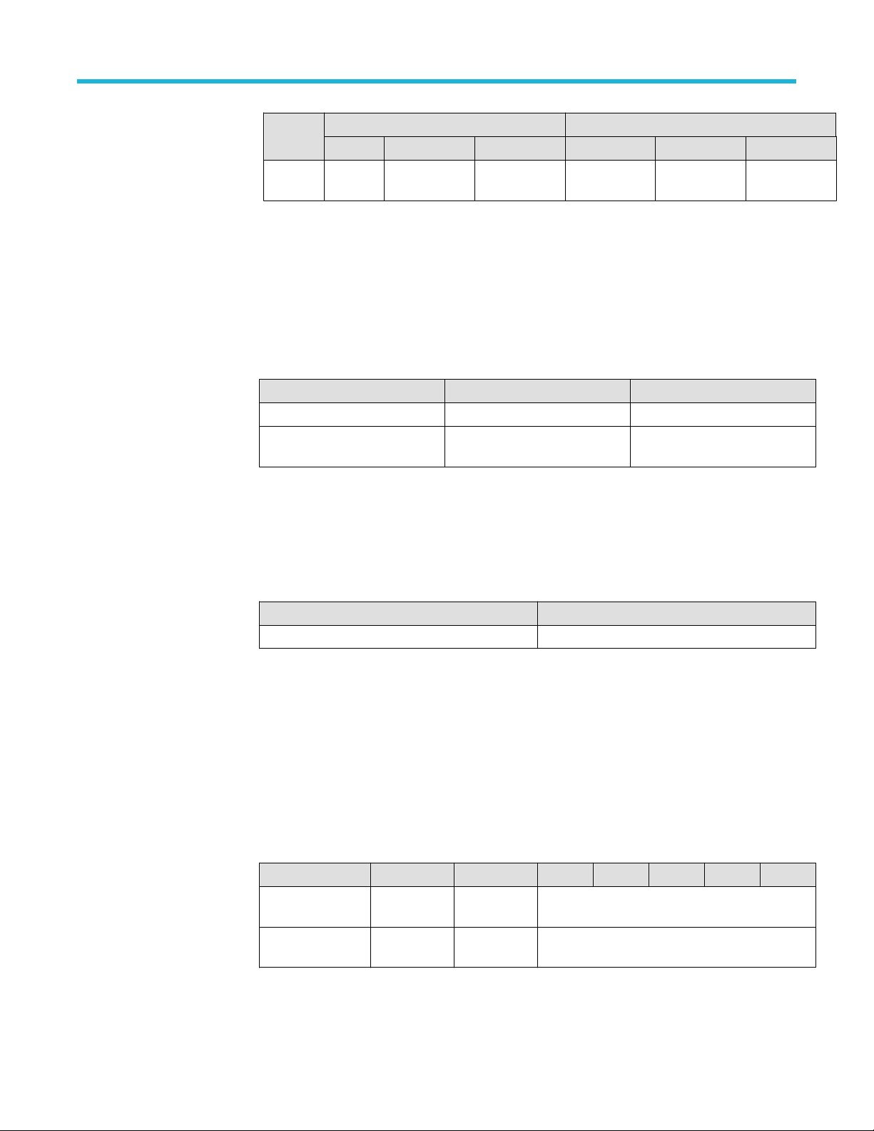
Timebase system
Test Title
Sample rate
Interpolated waveform rate
range
Record length range
Standard 1 kpoints to 125 Mpoints in single sample increments
Standard 1 kpoints to 62.5 Mpoints in single sample increments
Optional 5-RL-125M 125 Mpoints
Max HW Capability Number of Channels
6.25 GS/s 1- 8
500 GS/sec, 250 GS/sec, 125 GS/sec, 62.5 GS/sec, 25 GS/sec, and 12.5 GS/sec
Seconds-Division range
Seconds/Division range
Model 1 K 10 K 100 K 1 M 10 M 62.5 M 125 M
MSO5X Standard
62.5 M
MSO5X Option 5RL-125M
200 ps - 64 s 200 ps - 640 s 200 ps - 1000 s
200 ps - 64 s 200 ps - 640 s 200 ps - 1000 s
5 Series MSO MSO54, MSO56, MSO58, MSO58LP Specifications and Performance Verification 19
Page 20
Maximum acquisition rate
Specifications
Maximum triggered acquisition
rate, typical
Aperture uncertainty
✓Timebase accuracy
Analog or digital channels: single channel [Analog or Digital 8-bit channel] on screen, measurements and
math turned off. >40 wfm/sec
FastAcq Update Rate (analog only): >500 K/second with one channel active and >100 K/second with all
eight active.
FastAcq Update Rate (analog and analog/digital): >400 K/second with two channels active and >100
K/second with all eight analog channels active.
Digital channel: >40/second with one channel (8-bits) active. There is no FastAcq for digital channels, but
they do not slow down FastAcq for active analog channels.
≤ 0.450 ps + (1 * 10
-11
* Measurement Duration)
, for measurements having duration ≤ 100 ms
RMS
±2.5 x 10⁻⁶ over any ≥1 ms time interval
Description Specification
Factory Tolerance
±5.0 x10
-7
At calibration, 23 °C ambient, over any ≥1 ms interval
Temperature stability
±5.0 x10
-7
Tested at operating temperatures
Crystal aging
±1.5 x 10
-6
Frequency tolerance change at 25 °C over a period of 1 year
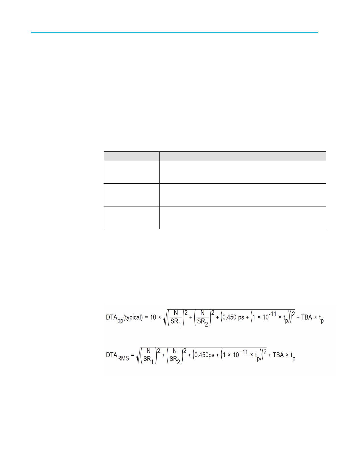
✓Delta-time measurement
accuracy
The formula to calculate delta-time measurement accuracy (DTA) for a given instrument setting and input
signal is as follows (assumes insignificant signal content above Nyquist frequency):
SR 1 = Slew Rate (1st Edge) around 1st point in measurement
SR 2 = Slew Rate (2nd Edge) around 2nd point in measurement
N = input-referred guaranteed noise limit (V
RMS
)
TBA = timebase accuracy or Reference Frequency Error
t p = delta-time measurement duration (sec)
(assume edge shape that results from Gaussian filter response)
The term under the square root sign is the stability and is due to TIE (Time Interval Error). The errors due
to this term occur throughout a single-shot measurement. The second term is due to both the absolute
center-frequency accuracy and the center-frequency stability of the timebase and varies between multiple
5 Series MSO MSO54, MSO56, MSO58, MSO58LP Specifications and Performance Verification 20
Page 21
Trigger system
Specifications
single-shot measurements over the observation interval (the amount of time from the first single-shot
measurement to the final single-shot measurement).
Note: The formulas assume negligible errors due to measurement interpolation, and apply only
when the interpolated sample rate is 25 GS/s or higher.
Trigger bandwidth (edge, pulse
and logic), typical
Edge-type trigger sensitivity,
DC coupled, typical
2 GHz models, Edge 2 GHz
2 GHz models, Pulse and
Logic
1 GHz models including
MSO58LP
500 MHz models 500 MHz
350 MHz models 350 MHz
1 GHz
1 GHz
Table 1: 5 Series MSO
Path Range Specification
1 MΩ path (all
models)
50 Ω path, 1
GHz, 500
MHz, 350 MHz
models
50 Ω path, 2
GHz models
Line Fixed
0.5 mV/div to 0.99
mV/div
≥ 1 mV/div The greater of 5 mV or 0.7 div from DC to lesser of 500 MHz or
0.5 mV/div to 0.99
mV/div
1 mV/div to 9.98
mV/div
≥ 10 mV/div < 1.0 division from DC to instrument bandwidth
5 mV from DC to instrument bandwidth
instrument BW, & 6 mV or 0.8 div from > 500 MHz to instrument
bandwidth
The greater of 5.6 mV or 0.7 div from DC to the lesser of 500
MHz or instrument BW, & 7 mV or 0.8 div from > 500 MHz to
instrument bandwidth
3.0 div from DC to instrument bandwidth
1.5 divisions from DC to instrument bandwidth
Table 2: MSO58LP
Path Range Specification
1 MΩ path (all
models)
Table continued…
5 Series MSO MSO54, MSO56, MSO58, MSO58LP Specifications and Performance Verification 21
0.5 mV/div to 0.99
mV/div
≥ 1 mV/div The greater of 5 mV or 0.7 div from DC to lesser of 500 MHz or
4.5 div from DC to instrument bandwidth
instrument BW, & 6 mV or 0.8 div from > 500 MHz to instrument
bandwidth
Page 22

Specifications
Path Range Specification
50 Ω path The greater of 5.6 mV or 0.7 div from DC to the lesser of 500
MHz or instrument BW, & 7 mV or 0.8 div from > 500 MHz to
instrument bandwidth
Line Fixed
AUX Trigger in 200 mVPP, DC to 250 MHz
Trigger jitter, typical ≤ 5 ps
≤ 7 ps
≤ 40 ps
≤ 200 ps
≤ 220 ps
AUX In trigger skew between
instruments, typical (MSO58LP
only)
Edge-type trigger sensitivity,
not DC coupled, typical
±100 ps jitter on each instrument with 150 ps skew; ≤350 ps total between instruments.
Skew improves for sinusoidal input voltages ≥500 mV
Trigger Coupling Typical Sensitivity
for sample mode and edge-type trigger
RMS
for edge-type trigger and FastAcq mode
RMS
for non edge-type trigger modes
RMS
for AUX trigger in, Sample acquisition mode, edge trigger (MSO58LP only)
RMS
for AUX trigger in, FastAcq acquisition mode, edge trigger (MSO58LP only)
RMS
NOISE REJ 2.5 times the DC Coupled limits
HF REJ 1.0 times the DC Coupled limits from DC to 50 kHz. Attenuates signals above
50 kHz.
LF REJ 1.5 times the DC Coupled limits for frequencies above 50 kHz. Attenuates
signals below 50 kHz.
Lowest frequency for successful operation of Set Level to 50% function
Lowest frequency for
successful operation of Set
Level to 50% function, typical
45 Hz
Logic-type or logic qualified trigger or events-delay sensitivities, DC coupled
Logic-type, logic qualified
trigger, or events-delay
sensitivities, DC coupled,
typical
2.0 divisions, at vertical settings ≥5 mV/div.
Pulse-type runt trigger sensitivities
Pulse-type runt trigger
sensitivities, typical
2.0 division at vertical settings ≥5 mV/div.
Pulse-type trigger width and glitch sensitivities
Pulse-type trigger width and
glitch sensitivities, typical
5 Series MSO MSO54, MSO56, MSO58, MSO58LP Specifications and Performance Verification 22
2.0 divisions at vertical settings ≥5 mV/div.
Page 23
Specifications
Logic-type triggering,
minimum logic or rearm time,
typical
Minimum clock pulse widths
for setup/hold time violation
trigger, typical
Setup/hold violation trigger,
setup and hold time ranges,
typical
Triggering type Pulse width Rearm time Time skew needed for 100%
5
7
Logic 160 ps + t
Time qualified logic 320 ps + t
t
is rise time of the instrument.
rise
Minimum pulsewidth, clock active
320 ps + t
t
rise
rise
is rise time of the instrument.
rise
rise
and no triggering
160 ps + t
320 ps + t
6
rise
rise
Minimum pulsewidth, clock inactive
320 ps +t
rise
>360 ps / <150 ps
>360 ps / <150 ps
Feature Min Max
Setup Time 0 ns 20 s
Hold Time 0 ns 20 s
Setup + Hold Time 320 ps 22 s
Input coupling on clock and data channels must be the same.
For Setup Time, positive numbers mean a data transition before the clock.
For Hold Time, positive numbers mean a data transition after the clock edge.
Pulse type trigger, minimum
pulse, rearm time, transition
time
Setup + Hold Time is the algebraic sum of the Setup Time and the Hold Time programmed by the user.
Pulse class Minimum pulse width Minimum rearm time
Runt 160 ps + t
Time-Qualified Runt 160 ps + t
Width 160 ps + t
Slew Rate (minimum transition
160 ps + t
rise
rise
rise
rise
160 ps + t
160 ps + t
160 ps + t
160 ps + t
rise
rise
rise
rise
time)
For trigger class width, pulse width refers to the width of the pulse being measured. Rearm time refers to the
time between pulses.
For trigger class runt, pulse width refers to the width of the pulse being measured. Rearm time refers to the
time between pulses.
For trigger class slew rate, pulse width refers to the delta time being measured. Rearm time refers to the
time it takes the signal to cross the two trigger thresholds again.
t
is rise time of the instrument.
rise
Active pulsewidth is the width of the clock pulse from its active edge (as defined in the Clock Edge menu
item) to its inactive edge
5
For Logic, time between channels refers to the length of time a logic state derived from more than one channel must exist to be recognized. For Events, the time is
the minimum time between a main and delayed event that will be recognized if more than one channel is used.
6
Active pulsewidth is the width of the clock pulse from its active edge (as defined in the Clock Edge menu item) to its inactive edge.
7
Inactive pulsewidth is the width of the pulse from its inactive edge to its active edge.
5 Series MSO MSO54, MSO56, MSO58, MSO58LP Specifications and Performance Verification 23
Page 24
Inactive pulsewidth is the width of the pulse from its inactive edge to its active edge.
Specifications
Transition time trigger, delta
160 ps to 20 s.
time range
Time range for glitch, pulse
160 ps to 20 s.
width, timeout, time-qualified
runt, or time-qualified window
triggering
Time accuracy for pulse,
glitch, timeout, or width
triggering
Time Range Accuracy
1 ns to 500 ns ±(160 ps +Time Base Error * Setting).
520 ns to 1 s ±(160 ps +Time Base Error * Setting).
B trigger after events,
minimum pulse width and
maximum event frequency,
typical
B trigger, minimum time
between arm and trigger,
typical
Minimum pulse width: 160 ps + t
Maximum event frequency: Instrument bandwidth.
t
is rise time of the instrument.
rise
320 ps
For trigger after time, this is the time between the end of the time period and the B trigger event.
For trigger after events, this is the time between the last A trigger event and the first B trigger event.
B trigger after time, time range 160 ps to 20 seconds
rise
B trigger after events, event
1 to 65,471
range
Trigger level ranges
Source Range
Any Channel ±5 divs from center of screen
Line Fixed at about 50% of line voltage
Source Range
Any Channel ±5 divs from center of screen
Aux In Trigger ±5 V
Line Fixed at about 50% of line voltage
This specification applies to logic and pulse thresholds.
Trigger level accuracy DC coupled
Trigger level accuracy, DC
coupled, typical
For signals having rise and fall times ≥10 ns:
Source Range
Any Input Channel ±0.20 div
Line N/A
Trigger holdoff range 0 ns to 10 seconds
5 Series MSO MSO54, MSO56, MSO58, MSO58LP Specifications and Performance Verification 24
Page 25

Serial Trigger specifications
Maximum serial trigger bits 128 bits
Optional serial bus interface triggering
Specifications
I2C
SPI Data Trigger: 1 - 16 Bytes of user-specified data
CAN Data Trigger: 1 - 8 Bytes of user-specified data, including qualifiers of equal to (=), not equal to (≠), less than
LIN Identifier Trigger: 6 bits of user-specified data, equal to (=)
Address Triggering: 7 & 10 bits of user-specified addresses supported
Data Trigger: 1 - 5 Bytes of user-specified data
Trigger on: Start, Repeated Start, Stop, Missing Ack, Data, Address, or Address & Data
Maximum Data Rate: 10 Mb/s
Trigger on: SS Active, Data
Maximum Data Rate: 20 Mb/s
(<), greater than (>), less than or equal to (<=), greater than or equal to (>=)
Trigger on: Start of Frame, Type of Frame, Identifier, Data, Identifier & Data, End of Frame, Missing Ack, or Bit
Stuffing Errors
Frame Type: Data, Remote, Error, Overload
Identifier: Standard (11 bit) and Extended (29 bit) identifiers
Maximum Data Rate: 1 Mb/s
Data Trigger: 1 - 8 Bytes of user-specified data, including qualifiers of equal to (=), not equal to (≠), less than
(<), greater than (>), less than or equal to (<=), greater than or equal to (>=), inside range, outside range
Error Trigger: Sync, Identifier Parity, Checksum
Trigger on: Sync, Identifier, Data, Identifier & Data, Wakeup Frame, Sleep Frame, or Error
Maximum Data Rate: 100 kb/s
Flexray Indicator Bits: Normal (01XX), Payload (11XX), Null (00XX), Sync (XX10), Startup (XX11)
Frame ID Trigger: 11 bits of user-specified data, including qualifiers of equal to (=), not equal to (≠), less than
(<), greater than (>), less than or equal to (<=), greater than or equal to (>=)
Cycle Count Trigger: 6 bits of user-specified data , including qualifiers of equal to (=), not equal to (≠), less
than (<), greater than (>), less than or equal to (<=), greater than or equal to (>=)
Header Fields Trigger: 40 bits of user-specified data comprising Indicator Bits, Identifier, Payload Length,
Header CRC, and Cycle Count, equal to (=)
Data Trigger: 1 - 16 Bytes of user-specified data, with 0 to 253, or "don't care" bytes of data offset,including
qualifiers of equal to (=), not equal to (≠), less than (<), greater than (>), less than or equal to (<=), greater than
or equal to (>=), Inside Range, Outside Range
End Of Frame: User-chosen types Static, Dynamic (DTS), and All
Error Trigger: Header CRC, Trailer CRC, Null Frame-static, Null Frame-dynamic, Sync Frame, Startup frame
(No Sync)
5 Series MSO MSO54, MSO56, MSO58, MSO58LP Specifications and Performance Verification 25
Page 26

Specifications
Trigger on: Start of Frame, Frame ID, Indicator Bits, Cycle Count, Header Fields, Data, Identifier & Data, End
of Frame, or Error
Maximum Data Rate: 40 Mb/s
Audio (I2S)
Data Trigger: 32 bits of user-specified data in a left word, right word, or either, including qualifiers of equal to
(=), not equal to (≠), less than (<), greater than (>), less than or equal to (<=), greater than or equal to (>=),
inside range, outside range
Trigger on: Word Select, Data
Maximum Data Rate: 12.5 Mb/s
Left Justified (LJ)
Data Trigger: 32 bits of user-specified data in a left word, right word, or either, including qualifiers of equal to
(=), not equal to (≠), less than (<), greater than (>), less than or equal to (<=), greater than or equal to (>=),
inside range, outside range
Trigger on: Word Select, Data
Maximum Data Rate: 12.5 Mb/s
Right Justified (RJ)
Data Trigger: 32 bits of user-specified data in a left word, right word, or either, including qualifiers of equal to
(=), not equal to (≠), less than (<), greater than (>), less than or equal to (<=), greater than or equal to (>=),
inside range, outside range
Trigger on: Word Select, Data
Maximum Data Rate: 12.5 Mb/s
TDM
Data Trigger: 32 bits of user-specified data in a channel 1-64, including qualifiers of equal to (=), not equal
to (≠), less than (<), greater than (>), less than or equal to (<=), greater than or equal to (>=), inside range,
outside range
Trigger on: Frame Sync, Data
Maximum Data Rate: 25 Mb/s
RS232 Bit Rate: 50 bps - 10 Mbps
Data Bits: 7, 8, or 9
Parity: None, Odd, or Even
Trigger on: Start, End of Packet, Data, Parity Error
MIL-STD-1553 Bit Rate: 1 Mb/s
Trigger on:
Sync
Word Type (Command, Status, Data)
Command Word (set RT Address (=, ≠, <, >, ≤, ≥, inside range, outside range), T/R, Sub-address/ Mode, Data
Word Count/Mode Code, and Parity individually)
5 Series MSO MSO54, MSO56, MSO58, MSO58LP Specifications and Performance Verification 26
Page 27

Status Word (set RT Address ((=, ≠, <, >, ≤, ≥, inside range, outside range), Message Error, Instrumentation,
Service Request Bit, Broadcast Command Received, Busy, Subsystem Flag, Dynamic Bus Control Acceptance
(DBCA), Terminal Flag, and Parity individually)
Data Word (user-specified 16-bit data value)
Error (Sync, Parity, Manchester, Non-contiguous data)
Idle Time (minimum time selectable from 4 μs to 100 μs; maximum time selectable from 12 μs to 100 μs;
trigger on < minimum, > maximum, inside range, outside range)
For MIL-STD-1553, Trigger selection of Command Word will trigger on Command and ambiguous Command/
Status words. Trigger selection of Status Word will trigger on Status and ambiguous Command/Status words
USB Data Rates Supported: High: 480 Mbs, Full: 12 Mbs, Low: 1.5Mbs
Trigger On: Sync, Reset, Suspend, Resume, End of Packet, Token Packet, Data Packet, Handshake Packet,
Special Packet, Error
Ethernet Bit Rate: 10 BASE-T, 10 Mbps; 100 BASE-TX, 100 Mbps
Trigger On: Start of Frame, MAC Address, MAC Length/Type, IP Header, TCP Header, Client Data, End of
Packet, Idle, FCS (CRC) Error, MAC Q-Tag control Information
Specifications
Digital acquisition system
Digital channel maximum
sample rate
Transition detect (digital peak
detect)
Digital-To-Analog trigger skew 1 ns
Digital to digital skew 320 ps from bit 0 of any TekVPI channel to bit 0 of any TekVPI channel.
Digital skew within a
FlexChannel
6.25 GS/s
Displayed data at sample rates less than 6.25 GS/s (decimated data), that contains multiple transitions
between sample points will be displayed with a bright white colored edge.
160 ps within any TekVPI channel
Digital volt meter (DVM)
Measurement types DC, AC
Voltage resolution 4 digits
✓Voltage accuracy
DC: ±((1.5% * |reading - offset - position|) + (0.5% * |(offset - position)|) + (0.1 * Volts/div))
De-rated at 0.100%/°C of |reading - offset - position| above 30 °C
RMS
+DC, AC
RMS
Signal ± 5 divisions from screen center
AC: ± 2% (40 Hz to 1 kHz) with no harmonic content outside 40 Hz to 1 kHz range
AC, typical: ± 2% (20 Hz to 10 kHz)
5 Series MSO MSO54, MSO56, MSO58, MSO58LP Specifications and Performance Verification 27
Page 28

Specifications
For AC measurements, the input channel vertical settings must allow the VPP input signal to cover between 4
and 10 divisions and must be fully visible on the screen
Trigger frequency counter
✓Accuracy ±(1 count + time base accuracy * input frequency)
The signal must be at least 8 mVpp or 2 div, whichever is greater.
✓ Maximum input frequency 10 Hz to maximum bandwidth of the analog channel
The signal must be at least 8 mVpp or 2 div, whichever is greater.
Resolution 8-digits
Arbitrary Function Generator system
Function types Arbitrary, sine, square, pulse, ramp, triangle, DC level, Gaussian, Lorentz, exponential rise/fall, sin(x)/x,
random noise, Haversine, Cardiac
Amplitude range Values are peak-to-peak voltages
Waveform 50 Ω 1 MΩ
Arbitrary 10 mV to 2.5 V 20 mV to 5 V
Sine 10 mV to 2.5 V 20 mV to 5 V
Square 10 mV to 2.5 V 20 mV to 5 V
Pulse 10 mV to 2.5 V 20 mV to 5 V
Ramp 10 mV to 2.5 V 20 mV to 5 V
Triangle 10 mV to 2.5 V 20 mV to 5 V
Gaussian 10 mV to 1.25 V 20 mV to 2.5 V
Lorentz 10 mV to 1.2 V 20 mV to 2.4 V
Exponential Rise 10 mV to 1.25 V 20 mV to 2.5 V
Exponential Fall 10 mV to 1.25 V 20 mV to 2.5 V
Sine(x)/x 10 mV to 1.5 V 20 mV to 3.0 V
Random Noise 10 mV to 2.5 V 20 mV to 5 V
Haversine 10 mV to 1.25 V 20 mV to 2.5 V
Cardiac 10 mV to 2.5 V 20 mV to 5 V
Maximum sample rate 250 MS/s
Arbitrary function record
length
Sine waveform
Frequency range 0.1 Hz to 50 MHz
5 Series MSO MSO54, MSO56, MSO58, MSO58LP Specifications and Performance Verification 28
128 K Samples
Page 29

Specifications
Frequency setting
0.1 Hz
resolution
Frequency accuracy 130 ppm (frequency ≤ 10 kHz), 50 ppm (frequency > 10 kHz)
This is for Sine, Ramp, Square and Pulse waveforms only.
Amplitude range 20 mVpp to 5 Vpp into Hi-Z; 10 mVpp to 2.5 Vpp into 50 Ω
Amplitude flatness, typical ±0.5 dB at 1 kHz
±1.5 dB at 1 kHz for < 20 mVpp amplitudes
Total harmonic distortion,
typical
1% for amplitude ≥ 200 mVpp into 50 Ω load
2.5% for amplitude > 50 mV AND < 200 mVpp into 50 Ω load
This is for Sine wave only.
Spurious free dynamic
40 dB (Vpp ≥ 0.1 V); 30 dB (Vpp ≥ 0.02 V), 50 Ω load
range, typical
Square and pulse waveform
Frequency range 0.1 Hz to 25 MHz
Frequency setting
0.1 Hz
resolution
Duty cycle range 10% - 90% or 10 ns minimum pulse, whichever is larger
Minimum pulse time applies to both on and off time, so maximum duty cycle will reduce at higher frequencies
to maintain 10 ns off time
Duty cycle resolution 0.1%
Minimum pulse width,
10 ns. This is the minimum time for either on or off duration.
typical
Rise/Fall time, typical 5 ns, 10% - 90%
Pulse width resolution 100 ps
Overshoot, typical < 6% for signal steps greater than 100 mV
This applies to overshoot of the positive-going transition (+overshoot) and of the negative-going (-overshoot)
transition
Asymmetry, typical ±1% ±5 ns, at 50% duty cycle
Jitter, typical < 60 ps TIE
, ≥ 100 mVpp amplitude, 40%-60% duty cycle
RMS
Ramp and triangle waveform
Frequency range 0.1 Hz to 500 kHz
Frequency setting
0.1 Hz
resolution
Variable symmetry 0% - 100%
Symmetry resolution 0.1%
pp
DC level range ±2.5 V into Hi-Z
±1.25 V into 50 Ω
5 Series MSO MSO54, MSO56, MSO58, MSO58LP Specifications and Performance Verification 29
Page 30

Gaussian pulse, Haversine, and Lorentz pulse
Maximum frequency 5 MHz
Specifications
Exponential rise fall maximum
frequency
Sin(x)/x
Maximum frequency 2 MHz
Random noise amplitude
range
✓Sine and ramp frequency
accuracy
✓Square and pulse frequency
accuracy
Signal amplitude resolution 1 mV (Hi-Z)
✓Signal amplitude accuracy ±[ (1.5% of peak-to-peak amplitude setting) + (1.5% of absolute DC offset setting) + 1 mV ] (frequency = 1
5 MHz
20 mVpp to 5 Vpp into Hi-Z
10 mVpp to 2.5 Vpp into 50 Ω
For both isolated noise signal and additive noise signal.
1.3 x 10⁻⁴ (frequency ≤10 kHz)
5.0 x 10⁻⁵ (frequency >10 kHz)
1.3 x 10⁻⁴ (frequency ≤10 KHz);
5.0 x 10⁻⁵ (frequency >10 KHz)
500 μV (50 Ω)
kHz)
DC offset range ±2.5 V into Hi-Z
±1.25 V into 50 Ω
DC offset resolution 1 mV (Hi-Z)
500 μV (50 Ω)
✓DC offset accuracy ±[ (1.5% of absolute offset voltage setting) + 1 mV ]
Add 3 mV of uncertainty per 10 °C change from 25 °C ambient
Display system (MSO54, MSO56, MSO58)
Display type Display area - 13.55 inches (344.16 mm) (H) x 7.62 inches (193.59 mm) (V), 15.55 inches (395 mm)
diagonal, 6-bit RGB color, (1920 X 1080) TFT liquid crystal display (LCD) with capacitive touch
Display resolution 1,920 horizontal × 1,080 vertical pixels (High Definition)
Luminance, typical
250 cd/m2, (Minimum: 200 cd/m2 )
Display luminance is specified for a new display set at full brightness.
5 Series MSO MSO54, MSO56, MSO58, MSO58LP Specifications and Performance Verification 30
Page 31

Specifications
Waveform display color scale
Color support 262K (6-bit RGB) colors.
Processor system
Host processor Intel i5-4400E, 2.7 GHz, 64-bit, dual core processor
Operating system Default instrument: Closed Linux
Instrument with option 5-WIN installed: Microsoft Windows 10
8
Input/Output port specifications
Ethernet interface An 8-pin RJ-45 connector that supports 10/100/1000 Mb/s
Video signal output A 15-pin, 3-row, D-sub VGA connector.
Recommended resolution: 1920 x 1080 @ 60 Hz.
DVI connector A 29-pin DVI-D connector; connect to show the oscilloscope display on an external monitor or projector
Maximum supported resolution, Windows: 1920 x 1200 @ 60 Hz
Maximum supported resolution, Linux: 1920 x 1080 @ 60 Hz
Only a single TMDS link is provided
Analog VGA signaling is not provided
DisplayPort connector A 20-pin DisplayPort connector; connect to show the oscilloscope display on an external monitor or
projector
Maximum supported resolution, Windows: 2560 x 1440 @ 60Hz
Maximum supported resolution, Linux: 1920 x 1080 @ 60 Hz
DP++ adapter: Maximum supported resolution: 2560 x1440 @ 60 Hz
Simultaneous displays
Simultaneous displays Up to 3 displays (including the internal display) with a maximum of 1 display per port.
USB interface (Host, Device
ports)
5 Series MSO Front panel USB Host ports: Two USB 2.0 Hi-Speed ports, one USB 3.0 SuperSpeed port
MSO58LP Front panel USB Host ports: One USB 2.0 Hi-Speed port, one USB 3.0 SuperSpeed port
All instruments, Rear panel USB Host ports: Two USB 2.0 Hi-Speed ports, two USB 3.0 SuperSpeed ports
All instruments, Rear panel USB Device port: One USB 3.0 SuperSpeed Device port providing USBTMC
support
Probe compensator signal
output voltage and frequency,
typical
8
Option 5-WIN is not available for MSO58LP instrument.
5 Series MSO MSO54, MSO56, MSO58, MSO58LP Specifications and Performance Verification 31
Characteristic Value
Output Voltage Default: 0-2.5 V amplitude
Impedance 1 kΩ
Table continued…
Page 32

Specifications
Characteristic Value
Frequency 1 kHz
✓Auxiliary output, AUX OUT, Trigger Out, Event, or Reference Clock Out
Selectable output Acquisition Trigger Out
Reference Clock Out
AFG Trigger Out
Acquisition Trigger Out User selectable transition from HIGH to LOW, or LOW to HIGH, indicates the trigger occurred. The signal
returns to its previous state after approximately 100 ns
Acquisition trigger jitter 300 ps (peak-to-peak)
Reference Clock Out Reference clock output tracks the acquisition system and can be referenced from either the internal clock
reference or the external clock reference
AFG Trigger Out The output frequency is dependent on the frequency of the AFG signal as shown in the following table:
AFG signal frequency AFT trigger frequency
≤ 4.9 MHz Signal frequency
> 4.9 MHz to 14.7 MHz Signal frequency / 3
> 14.7 MHz to 24.5 MHz Signal frequency / 5
> 24.5 MHz to 34.3 MHz Signal frequency / 7
> 34.3 MHz to 44.1 MHz Signal frequency / 9
> 44.1 MHz to 50 MHz Signal frequency / 11
AUX OUT Output Voltage
External reference input
Nominal input frequency 10 MHz
Frequency Variation
Tolerance
Sensitivity, typical Vin 1.5 V
Maximum input signal 7 V
Impedance 1.2 K Ohms ±20% in parallel with 18 pf ±5 pf at 10 MHz
Characteristic Limits
Vout (HI) ≥ 2.5 V open circuit; ≥ 1.0 V into a 50 Ω load to ground
Vout (LO) ≤ 0.7 V into a load of ≤ 4 mA; ≤0.25 V into a 50 Ω load to ground
9.99996 MHz to 10.00004 MHz (±4.0 x 10⁻⁶)
using a 50 Ω termination
p-p
pp
Data storage specifications
Nonvolatile memory retention time typical
Nonvolatile memory retention
time, typical
No time limit for front panel settings, saved waveforms, setups, product licensing, and calibration constants.
5 Series MSO MSO54, MSO56, MSO58, MSO58LP Specifications and Performance Verification 32
Page 33

Specifications
Real-time clock
Real-time clock A programmable clock providing time in years, months, days, hours, minutes, and seconds.
Nonvolatile memory capacity
Nonvolatile memory capacity
Instrument S/N A 2 kbit EEPROM on the main board that stores the instrument serial number, instrument start up count, total
uptime and administration passwords.
Companion CvP A pair of 16 Mbit flash memory devices that stores a portion of the Companion FPGA image data. One device
serves as a backup for the other device.
AFG S/N A 2 kbit EEPROM on the AFG riser card that stores a copy of the instrument serial number which is used to
validate the AFG calibration.
Front Panel ID A 64 kbit EEPROM on the LED board that stores the USB vendor ID and device ID for the internal front panel
controller.
BIOS A 128 Mbit flash memory device that stores the firmware image and device configuration for the host processor
and chipset sub-processors. This includes the Basic Input Output System (BIOS), Management Engine (ME),
Embedded Controller (EC) and Network Interface Controller (NIC). The Ethernet MAC address is stored in this
device.
CMOS Memory The host processor chipset includes an integrated memory device, powered by the real-time clock (RTC)
battery, which stores BIOS configuration settings. A customer accessible switch disconnects the RTC battery
from the chipset which clears the contents of the integrated CMOS memory device.
Memory SPD Each SODIMM (memory module) contains a serial presence detect (SPD) memory device implemented using
an unspecified memory technology. Each SPD device contains the parameter data specific to its memory
module. All SPD devices are treated by the instrument as read only. The size of a given SPD is unspecified.
The 4 channel instrument includes 4 SPD devices. The 6 channel and 8 channel instruments include 6 SPD
devices.
UCD9248 The instrument includes 3 UCD9248 power supply controllers. Each controller contains an unspecified quantity
of nonvolatile memory that stores various power supply configuration settings.
PMU A power management unit (PMU) microcontroller is used to manage instrument power supplies and hardware
initialization. The PMU includes 32 KB of nonvolatile memory for storage of its own binary executable and
redundant storage of UCD9248 device settings.
Analog Board Controller A microcontroller is used to manage analog board operation. The PMU includes 64 KB of nonvolatile memory
for storage of its own binary executable.
Carrier FPGA The carrier FPGA stores its own configuration in its own internal 0.33 Mbit nonvolatile memory. The carrier
FPGA implements simple "glue logic" for the instrument.
Mass storage device capacity
Mass storage device capacity
Linux ≥80 GB. Form factor is an 80 mm m.2 card with a SATA-3 interface. Waveforms and setups are stored on a
hard disk drive or solid state drive. Provides storage for saved customer data, all calibration constants and the
Linux operating system. Not customer serviceable. A ~42 GB partition on the device is available for the storage
of saved customer data.
Windows (optional): ≥ 480 GB. Form factor is a 2.5-inch SSD with a SATA-3 interface. This drive is customer installable and
provides storage for the Windows operating system option, and saved customer data. Not available for
MSO58LP.
5 Series MSO MSO54, MSO56, MSO58, MSO58LP Specifications and Performance Verification 33
Page 34

Power supply system
Power
Power consumption 400 Watts maximum
Source voltage 100 - 240 V ±10% (50 Hz to 60 Hz)
Source frequency 50 Hz to 60 Hz ±10%, at 100 - 240 V ±10%
400 Hz ±10% at 115 V ±10%
Specifications
Fuse Rating 12.5 A, 250 V
ac
Safety characteristics
Safety certification US NRTL Listed - UL61010-1.
Canadian Certification - CAN/CSA-C22.2 No. 61010.1.
EU Compliance - Low Voltage Directive 2014-35-EU and EN61010-1.
International Compliance - IEC 61010-1.
Pollution degree Pollution degree 2, indoor, dry location use only
Environmental specifications
Temperature
Operating +0 °C to +50 °C (32 °F to 122 °F)
Non-operating -20 °C to +60 °C (-4 °F to 140 °F)
Humidity
Operating 5% to 90% relative humidity (% RH) at up to +40 °C
5% to 55% RH above +40 °C up to +50 °C, noncondensing, and as limited by a maximum wet-bulb
temperature of +39 °C
Non-operating 5% to 90% relative humidity (% RH) at up to +40 °C
5% to 39% RH above +40 °C up to +50 °C, noncondensing, and as limited by a maximum wet-bulb
temperature of +39 °C
Altitude
Operating Up to 3,000 meters (9,843 feet)
Non-operating Up to 12,000 meters (39,370 feet)
Random Vibration, MSO58LP
Random vibration
Operating 0.31 GRMS, 5-500 Hz, 10 minutes per axis, 3 axes (30 minutes total)
Non-operating 2.46 GRMS, 5-500 Hz, 10 minutes per axis, 3 axes (30 minutes total)
5 Series MSO MSO54, MSO56, MSO58, MSO58LP Specifications and Performance Verification 34
Page 35

Mechanical specifications
Dimensions, 5 Series MSO Height: 12.2 in (309 mm), feet folded in, handle to back
Height: 14.6 in (371 mm) feet folded in, handle up
Width: 17.9 in (454 mm) from handle hub to handle hub
Depth: 8.0 in (205 mm) from back of feet to front of knobs, handle up
Depth: 11.7 in (297.2 mm) feet folded in, handle to the back
Dimensions, MSO58LP Height: 3.44 in (87.3 mm)
Width: 17.01 in (432 mm)
Depth: 23.85 in (605.7 mm)
Fits rack depths from 24 inches to 32 inches
Weight, 5 Series MSO MSO54 1 GHz, 500 MHz, 350 MHz models: 22.7 lbs (10.3 kg)
MSO54 2 GHz models: 23.6 lbs (10.7 kg)
MSO56 1 GHz, 500 MHz, 350 MHz models: 23.5 lbs (10.7 kg)
MSO56 2 GHz models: 24.3 lbs (11 kg)
Specifications
MSO58 1 GHz, 500 MHz, 350 MHz models: 23.8 lbs (10.8 kg)
MSO58 2 GHz models: 24.7 lbs (11.2 kg)
Front cover without pouch: 1.9 lbs (0.86 kg)
Front cover with pouch: 3.1 lbs (1.4 kg)
Weight, MSO58LP 25.5 lbs (11.6 kg)
Cooling , 5 Series MSO The clearance requirement for adequate cooling is 2.0 in (50.8 mm) on the right side of the instrument
(when viewed from the front) and on the rear of the instrument
Cooling, MSO58LP The clearance requirement for adequate cooling is 2.0 in (50.8 mm) on the left and right sides of the
instrument (when viewed from the front). Air flows through the instrument from left to right
5 Series MSO MSO54, MSO56, MSO58, MSO58LP Specifications and Performance Verification 35
Page 36

Performance verification procedures
Performance verification procedures
This chapter contains performance verification procedures for the specifications marked with the symbol. The following equipment, or a
suitable equivalent, is required to complete these procedures.
The performance verification procedures verify the performance of your instrument. They do not adjust your instrument. If your instrument
fails any of the performance verification tests, repeat the failing test, verifying that the test equipment and settings are correct. If the
instrument continues to fail a test, contact Tektronix Customer Support for assistance.
These procedures cover all 5 Series MSO instruments (MSO54, MSO56, MSO58, MSO58LP).
Print the test records on the following pages and use them to record the performance test results for your oscilloscope. Disregard checks
and test records that do not apply to the specific model you are testing.
Note: Completion of the performance verification procedure does not update the instrument time and date.
Required equipment:
Required equipment Minimum requirements Examples
DC voltage source 3 mV to 4 V, ±0.1% accuracy Fluke 9500B Oscilloscope Calibrator with a
9530 Output Module
Leveled sine wave generator 50 kHz to 2 GHz, ±4% amplitude accuracy
Time mark generator
Logic probe Low capacitance digital probe, 8 channels. TLP058 probe
BNC-to-0.1 inch pin adapter to connect the
logic probe to the signal source.
Digital multimeter (DMM) 0.1% accuracy or better Tektronix DMM4020
One 50 Ω terminator Impedance 50 Ω; connectors: female BNC
One 50 Ω BNC cable Male-to-male connectors Tektronix part number 012-0057-01
Optical mouse USB, PS2 Tektronix part number 119-7054-00
RF vector signal generator Maximum bandwidth of instrument Tektronix TSG4100A
80 ms period, ±1.0 x 10⁻⁶ accuracy, rise time
<50 ns
BNC-to-0.1 inch pin adapter; female BNC to
2x16 .01 inch pin headers.
input, male BNC output
Tektronix adapter part number 878-1429-00;
to connect the Fluke 9500B to the TLP058
probe.
Tektronix part number 011-0049-02
You might need additional cables and adapters, depending on the actual test equipment you use.
Test records
Instrument information, self test record
Model Serial # Procedure performed by Date
Test Passed Failed
Self Test
5 Series MSO MSO54, MSO56, MSO58, MSO58LP Specifications and Performance Verification 36
Page 37

Performance verification procedures
Input Impedance test record
Input Impedance
Performance checks Vertical scale Low limit Test result High limit
All models
Channel 1 Input
Impedance, 1 MΩ
Channel 1 Input
Impedance, 50 Ω
Channel 2 Input
Impedance, 1 MΩ
Channel 2 Input
Impedance, 50 Ω
Channel 3 Input
Impedance, 1 MΩ
Channel 3 Input
Impedance, 50 Ω
Channel 4 Input
Impedance, 1 MΩ
Channel 4, Input
Impedance, 50 Ω
100 mV/div 990 kΩ 1.01 MΩ
10 mV/div 49.5 Ω 50.5 Ω
100 mV/div 49.5 Ω 50.5 Ω
100 mV/div 990 kΩ 1.01 MΩ
10 mV/div 49.5 Ω 50.5 Ω
100 mV/div 49.5 Ω 50.5 Ω
100 mV/div 990 kΩ 1.01 MΩ
10 mV/div 49.5 Ω 50.5 Ω
100 mV/div 49.5 Ω 50.5 Ω
100 mV/div 990 kΩ 1.01 MΩ
10 mV/div 49.5 Ω 50.5 Ω
100 mV/div 49.5 Ω 50.5 Ω
MSO56, MSO58, MSO58LP models
Channel 5 Input
Impedance, 1 MΩ
Channel 5 Input
Impedance, 50 Ω
Channel 6 Input
Impedance, 1 MΩ
Channel 6 Input
Impedance, 50 Ω
MSO58, MSO58LP models
Channel 7 Input
Impedance, 1 MΩ
Channel 7 Input
Impedance, 50 Ω
Channel 8 Input
Impedance, 1 MΩ
Channel 8, Input
Impedance, 50 Ω
100 mV/div 990 kΩ 1.01 MΩ
10 mV/div 49.5 Ω 50.5 Ω
100 mV/div 49.5 Ω 50.5 Ω
100 mV/div 990 kΩ 1.01 MΩ
10 mV/div 49.5 Ω 50.5 Ω
100 mV/div 49.5 Ω 50.5 Ω
100 mV/div 990 kΩ 1.01 MΩ
10 mV/div 49.5 Ω 50.5 Ω
100 mV/div 49.5 Ω 50.5 Ω
100 mV/div 990 kΩ 1.01 MΩ
10 mV/div 49.5 Ω 50.5 Ω
100 mV/div 49.5 Ω 50.5 Ω
5 Series MSO MSO54, MSO56, MSO58, MSO58LP Specifications and Performance Verification 37
Page 38

Performance verification procedures
DC Balance test record
DC Balance
Performance checks Vertical scale Low limit Test result High limit
All models
Channel 1 DC Balance, 50 Ω,
20 MHz BW
Channel 1 DC Balance, 1 MΩ,
20 MHz BW
Channel 1 DC Balance, 50 Ω,
250 MHz BW
Channel 1 DC Balance, 1 MΩ,
250 MHz BW
Channel 1 DC Balance, 50 Ω, FullBW20 mV/div -2 mV 2 mV
1 mV/div -0.2 mV 0.2 mV
2 mV/div -0.2 mV 0.2 mV
5 mV/div -0.5 mV 0.5 mV
10 mV/div -1 mV 1 mV
20 mV/div -2 mV 2 mV
49.8 mV/div -4.98 mV 4.98 mV
50 mV/div -5 mV 5 mV
100 mV/div -10 mV 10 mV
200 mV/div -20 mV 20 mV
500 mV/div -50 mV 50 mV
1 V/div -100 mV 100 mV
1 mV/div -0.2 mV 0.2 mV
2 mV/div -0.4 mV 0.4 mV
5 mV/div -1 mV 1 mV
10 mV/div -2 mV 2 mV
20 mV/div -4 mV 4 mV
100 mV/div -20 mV 20 mV
500 mV/div -100 mV 100 mV
1 V/div -200 mV 200 mV
10 V/div -2 V 2 V
20 mV/div -2 mV 2 mV
20 mV/div -4 mV 4 mV
Channel 1 DC Balance, 1 MΩ, FullBW20 mV/div -4 mV 4 mV
Channel 2 DC Balance, 50 Ω,
20 MHz BW
Table continued…
5 Series MSO MSO54, MSO56, MSO58, MSO58LP Specifications and Performance Verification 38
1 mV/div -0.2 mV 0.2 mV
2 mV/div -0.2 mV 0.2 mV
5 mV/div -0.5 mV 0.5 mV
10 mV/div -1 mV 1 mV
20 mV/div -2 mV 2 mV
49.8 mV/div -4.98 mV 4.98 mV
50 mV/div -5 mV 5 mV
Page 39

Performance verification procedures
DC Balance
Performance checks Vertical scale Low limit Test result High limit
100 mV/div -10 mV 10 mV
200 mV/div -20 mV 20 mV
500 mV/div -50 mV 50 mV
1 V/div -100 mV 100 mV
Channel 2 DC Balance, 1 MΩ,
20 MHz BW
Channel 2 DC Balance, 50 Ω,
250 MHz BW
Channel 2 DC Balance, 1 MΩ,
250 MHz BW
Channel 2 DC Balance, 50 Ω, FullBW20 mV/div -2 mV 2 mV
1 mV/div -0.2 mV 0.2 mV
2 mV/div -0.4 mV 0.4 mV
5 mV/div -1 mV 1 mV
10 mV/div -2 mV 2 mV
20 mV/div -4 mV 4 mV
100 mV/div -20 mV 20 mV
500 mV/div -100 mV 100 mV
1 V/div -200 mV 200 mV
10 V/div -2 V 2 V
20 mV/div -2 mV 2 mV
20 mV/div -4 mV 4 mV
Channel 2 DC Balance, 1 MΩ, FullBW20 mV/div -4 mV 4 mV
Channel 3 DC Balance, 50 Ω,
20 MHz BW
Channel 3 DC Balance, 1 MΩ,
20 MHz BW
Table continued…
1 mV/div -0.2 mV 0.2 mV
2 mV/div -0.2 mV 0.2 mV
5 mV/div -0.5 mV 0.5 mV
10 mV/div -1 mV 1 mV
20 mV/div -2 mV 2 mV
49.8 mV/div -4.98 mV 4.98 mV
50 mV/div -5 mV 5 mV
100 mV/div -10 mV 10 mV
200 mV/div -20 mV 20 mV
500 mV/div -50 mV 50 mV
1 V/div -100 mV 100 mV
1 mV/div -0.2 mV 0.2 mV
2 mV/div -0.4 mV 0.4 mV
5 mV/div -1 mV 1 mV
10 mV/div -2 mV 2 mV
20 mV/div -4 mV 4 mV
5 Series MSO MSO54, MSO56, MSO58, MSO58LP Specifications and Performance Verification 39
Page 40

Performance verification procedures
DC Balance
Performance checks Vertical scale Low limit Test result High limit
100 mV/div -20 mV 20 mV
500 mV/div -100 mV 100 mV
1 V/div -200 mV 200 mV
10 V/div -2 V 2 V
Channel 3 DC Balance, 50 Ω,
250 MHz BW
Channel 3 DC Balance, 1 MΩ,
250 MHz BW
Channel 3 DC Balance, 50 Ω, FullBW20 mV/div -2 mV 2 mV
Channel 3 DC Balance, 1 MΩ, FullBW20 mV/div -4 mV 4 mV
20 mV/div -2 mV 2 mV
20 mV/div -4 mV 4 mV
Channel 4 DC Balance, 50 Ω,
20 MHz BW
Channel 4 DC Balance, 1 MΩ,
20 MHz BW
Channel 4 DC Balance, 50 Ω,
250 MHz BW
Channel 4 DC Balance, 1 MΩ,
250 MHz BW
Channel 4 DC Balance, 50 Ω, FullBW20 mV/div -2 mV 2 mV
1 mV/div -0.2 mV 0.2 mV
2 mV/div -0.2 mV 0.2 mV
5 mV/div -0.5 mV 0.5 mV
10 mV/div -1 mV 1 mV
20 mV/div -2 mV 2 mV
49.8 mV/div -4.98 mV 4.98 mV
50 mV/div -5 mV 5 mV
100 mV/div -10 mV 10 mV
200 mV/div -20 mV 20 mV
500 mV/div -50 mV 50 mV
1 V/div -100 mV 100 mV
1 mV/div -0.2 mV 0.2 mV
2 mV/div -0.4 mV 0.4 mV
5 mV/div -1 mV 1 mV
10 mV/div -2 mV 2 mV
20 mV/div -4 mV 4 mV
100 mV/div -20 mV 20 mV
500 mV/div -100 mV 100 mV
1 V/div -200 mV 200 mV
10 V/div -2 V 2 V
20 mV/div -2 mV 2 mV
20 mV/div -4 mV 4 mV
Table continued…
5 Series MSO MSO54, MSO56, MSO58, MSO58LP Specifications and Performance Verification 40
Page 41

Performance verification procedures
DC Balance
Performance checks Vertical scale Low limit Test result High limit
Channel 4 DC Balance, 1 MΩ, FullBW20 mV/div -4 mV 4 mV
MSO56, MSO58, MSO58LP models
Channel 5 DC Balance, 50 Ω,
20 MHz BW
Channel 5 DC Balance, 1 MΩ,
20 MHz BW
Channel 5 DC Balance, 50 Ω,
250 MHz BW
Channel 5 DC Balance, 1 MΩ,
250 MHz BW
Channel 5 DC Balance, 50 Ω, FullBW20 mV/div -2 mV 2 mV
1 mV/div -0.2 mV 0.2 mV
2 mV/div -0.2 mV 0.2 mV
5 mV/div -0.5 mV 0.5 mV
10 mV/div -1 mV 1 mV
20 mV/div -2 mV 2 mV
49.8 mV -4.98 mV/div 4.98 mV
50 mV/div -5 mV 5 mV
100 mV/div -10 mV 10 mV
200 mV/div -20 mV 20 mV
500 mV/div -50 mV 50 mV
1 V/div -100 mV 100 mV
1 mV/div -0.2 mV 0.2 mV
2 mV/div -0.4 mV 0.4 mV
5 mV/div -1 mV 1 mV
10 mV/div -2 mV 2 mV
20 mV/div -4 mV 4 mV
100 mV/div -20 mV 20 mV
500 mV/div -100 mV 100 mV
1 V/div -200 mV 200 mV
10 V/div -2 V 2 V
20 mV/div -2 mV 2 mV
20 mV/div -4 mV 4 mV
Channel 5 DC Balance, 1 MΩ, FullBW20 mV/div -4 mV 4 mV
Channel 6 DC Balance, 50 Ω,
20 MHz BW
Table continued…
5 Series MSO MSO54, MSO56, MSO58, MSO58LP Specifications and Performance Verification 41
1 mV/div -0.2 mV 0.2 mV
2 mV/div -0.2 mV 0.2 mV
5 mV/div -0.5 mV 0.5 mV
10 mV/div -1 mV 1 mV
20 mV/div -2 mV 2 mV
49.8 mV/div -4.98 mV 4.98 mV
Page 42

Performance verification procedures
MSO56, MSO58, MSO58LP models
50 mV/div -5 mV 5 mV
100 mV/div -10 mV 10 mV
200 mV/div -20 mV 20 mV
500 mV/div -50 mV 50 mV
1 V/div -100 mV 100 mV
Channel 6 DC Balance, 1 MΩ,
20 MHz BW
Channel 6 DC Balance, 50 Ω,
250 MHz BW
Channel 6 DC Balance, 1 MΩ,
250 MHz BW
Channel 6 DC Balance, 50 Ω, FullBW20 mV/div -2 mV 2 mV
1 mV/div -0.2 mV 0.2 mV
2 mV/div -0.4 mV 0.4 mV
5 mV/div -1 mV 1 mV
10 mV/div -2 mV 2 mV
20 mV/div -4 mV 4 mV
100 mV/div -20 mV 20 mV
500 mV/div -100 mV 100 mV
1 V/div -200 mV 200 mV
10 V/div -2 V 2 V
20 mV/div -2 mV 2 mV
20 mV/div -4 mV 4 mV
Channel 6 DC Balance, 1 MΩ, FullBW20 mV/div -4 mV 4 mV
MSO58, MSO58LP models
Channel 7 DC Balance, 50 Ω,
20 MHz BW
Channel 7 DC Balance, 1 MΩ,
20 MHz BW
Table continued…
1 mV/div -0.2 mV 0.2 mV
2 mV/div -0.2 mV 0.2 mV
5 mV/div -0.5 mV 0.5 mV
10 mV/div -1 mV 1 mV
20 mV/div -2 mV 2 mV
49.8 mV/div -4.98 mV 4.98 mV
50 mV/div -5 mV 5 mV
100 mV/div -10 mV 10 mV
200 mV/div -20 mV 20 mV
500 mV/div -50 mV 50 mV
1 V/div -100 mV 100 mV
1 mV/div -0.2 mV 0.2 mV
2 mV/div -0.4 mV 0.4 mV
5 mV/div -1 mV 1 mV
10 mV/div -2 mV 2 mV
5 Series MSO MSO54, MSO56, MSO58, MSO58LP Specifications and Performance Verification 42
Page 43

Performance verification procedures
MSO56, MSO58, MSO58LP models
20 mV/div -4 mV 4 mV
100 mV/div -20 mV 20 mV
500 mV/div -100 mV 100 mV
1 V/div -200 mV 200 mV
10 V/div -2 V 2 V
Channel 7 DC Balance, 50 Ω,
250 MHz BW
Channel 7 DC Balance, 1 MΩ,
250 MHz BW
Channel 7 DC Balance, 50 Ω, FullBW20 mV/div -2 mV 2 mV
Channel 7 DC Balance, 1 MΩ, FullBW20 mV/div -4 mV 4 mV
20 mV/div -2 mV 2 mV
20 mV/div -4 mV 4 mV
Channel 8 DC Balance, 50 Ω,
20 MHz BW
Channel 8 DC Balance, 1 MΩ,
20 MHz BW
Channel 8 DC Balance, 50 Ω,
250 MHz BW
Channel 8 DC Balance, 1 MΩ,
250 MHz BW
Channel 8 DC Balance, 50 Ω, FullBW20 mV/div -2 mV 2 mV
1 mV/div -0.2 mV 0.2 mV
2 mV/div -0.2 mV 0.2 mV
5 mV/div -0.5 mV 0.5 mV
10 mV/div -1 mV 1 mV
20 mV/div -2 mV 2 mV
49.8 mV/div -4.98 mV 4.98 mV
50 mV/div -5 mV 5 mV
100 mV/div -10 mV 10 mV
200 mV/div -20 mV 20 mV
500 mV/div -50 mV 50 mV
1 V/div -100 mV 100 mV
1 mV/div -0.2 mV 0.2 mV
2 mV/div -0.4 mV 0.4 mV
5 mV/div -1 mV 1 mV
10 mV/div -2 mV 2 mV
20 mV/div -4 mV 4 mV
100 mV/div -20 mV 20 mV
500 mV/div -100 mV 100 mV
1 V/div -200 mV 200 mV
10 V/div -2 V 2 V
20 mV/div -2 mV 2 mV
20 mV/div -4 mV 4 mV
Table continued…
5 Series MSO MSO54, MSO56, MSO58, MSO58LP Specifications and Performance Verification 43
Page 44

Performance verification procedures
MSO56, MSO58, MSO58LP models
Channel 8 DC Balance, 1 MΩ, FullBW20 mV/div -4 mV 4 mV
DC Gain Accuracy test record
DC Gain Accuracy, 2 GHz models
Performance
checks Bandwidth Vertical scale Low limit Test result High limit
Channel 1 DC Gain
Accuracy, 0 V offset,
0 V vertical position,
50 Ω
Channel 1 DC Gain
Accuracy, 0 V offset,
0 V vertical position,
1 MΩ
Channel 2 DC Gain
Accuracy, 0 V offset,
0 V vertical position,
50 Ω
Table continued…
20 MHz 1 mV/div -2% 2%
2 mV/div -1.2% 1.2%
5 mV/div -1.2% 1.2%
10 mV/div -1.2% 1.2%
20 mV/div -1.2% 1.2%
50 mV/div -1.2% 1.2%
100 mV/div -1.2% 1.2%
200 mV/div -1.2% 1.2%
500 mV/div -1.2% 1.2%
1 V/div -1.2% 1.2%
250 MHz 20 mV/div -1.2% 1.2%
FULL 20 mV/div -1.2% 1.2%
20 MHz 1 mV/div -2% 2%
2 mV/div -1% 1%
5 mV/div -1% 1%
10 mV/div -1% 1%
20 mV/div -1% 1%
50 mV/div -1% 1%
100 mV/div -1% 1%
200 mV/div -1% 1%
500 mV/div -1% 1%
1 V/div -1% 1%
250 MHz 20 mV/div -1% 1%
FULL 20 mV/div -1% 1%
20 MHz 1 mV/div -2% 2%
2 mV/div -1.2% 1.2%
5 mV/div -1.2% 1.2%
10 mV/div -1.2% 1.2%
20 mV/div -1.2% 1.2%
50 mV/div -1.2% 1.2%
100 mV/div -1.2% 1.2%
5 Series MSO MSO54, MSO56, MSO58, MSO58LP Specifications and Performance Verification 44
Page 45

Performance verification procedures
DC Gain Accuracy, 2 GHz models
Performance
checks Bandwidth Vertical scale Low limit Test result High limit
200 mV/div -1.2% 1.2%
500 mV/div -1.2% 1.2%
1 V/div -1.2% 1.2%
250 MHz 20 mV/div -1.2% 1.2%
FULL 20 mV/div -1.2% 1.2%
Channel 2 DC Gain
Accuracy, 0 V offset,
0 V vertical position,
1 MΩ
Channel 3 DC Gain
Accuracy, 0 V offset,
0 V vertical position,
50 Ω
Channel 3 DC Gain
Accuracy, 0 V offset,
0 V vertical position,
1 MΩ
Table continued…
20 MHz 1 mV/div -2% 2%
2 mV/div -1% 1%
5 mV/div -1% 1%
10 mV/div -1% 1%
20 mV/div -1% 1%
50 mV/div -1% 1%
100 mV/div -1% 1%
200 mV/div -1% 1%
500 mV/div -1% 1%
1 V/div -1% 1%
50 MHz 20 mV/div -1% 1%
FULL 20 mV/div -1% 1%
20 MHz 1 mV/div -2% 2%
2 mV/div -1.2% 1.2%
5 mV/div -1.2% 1.2%
10 mV/div -1.2% 1.2%
20 mV/div -1.2% 1.2%
50 mV/div -1.2% 1.2%
100 mV/div -1.2% 1.2%
200 mV/div -1.2% 1.2%
500 mV/div --1.2% 1.2%
1 V/div --1.2% 1.2%
250 MHz 20 mV/div -1.2% 1.2%
FULL 20 mV/div -1.2% 1.2%
20 MHz 1 mV/div -2% 2%
2 mV/div -1% 1%
5 mV/div -1% 1%
10 mV/div -1% 1%
20 mV/div -1% 1%
50 mV/div -1% 1%
5 Series MSO MSO54, MSO56, MSO58, MSO58LP Specifications and Performance Verification 45
Page 46

Performance verification procedures
DC Gain Accuracy, 2 GHz models
Performance
checks Bandwidth Vertical scale Low limit Test result High limit
100 mV/div -1% 1%
200 mV/div -1% 1%
500 mV/div -1% 1%
1 V/div -1% 1%
250 MHz 20 mV/div -1% 1%
FULL 20 mV/div -1% 1%
Channel 4 DC Gain
Accuracy, 0 V offset,
0 V vertical position,
50 Ω
Channel 4 DC Gain
Accuracy, 0 V offset,
0 V vertical position,
1 MΩ
20 MHz 1 mV/div -2% 2%
2 mV/div -1.2% 1.2%
5 mV/div -1.2% 1.2%
10 mV/div -1.2% 1.2%
20 mV/div -1.2% 1.2%
50 mV/div -1.2% 1.2%
100 mV/div -1.2% 1.2%
200 mV/div -1.2% 1.2%
500 mV/div -1.2% 1.2%
1 V/div -1.2% 1.2%
250 MHz 20 mV/div -1.2% 1.2%
FULL 20 mV/div -1.2% 1.2%
20 MHz 1 mV/div -2% 2%
2 mV/div -1% 1%
5 mV/div -1% 1%
10 mV/div -1% 1%
20 mV/div -1% 1%
50 mV/div -1% 1%
100 mV/div -1% 1%
200 mV/div -1% 1%
500 mV/div -1% 1%
1 V/div -1% 1%
250 MHz 20 mV/div -1% 1%
FULL 20 mV/div -1% 1%
MSO56 and MSO58 models
Channel 5 DC Gain
Accuracy, 0 V offset,
0 V vertical position,
50 Ω
Table continued…
5 Series MSO MSO54, MSO56, MSO58, MSO58LP Specifications and Performance Verification 46
20 MHz 1 mV/div -2% 2%
2 mV/div -1.2% 1.2%
5 mV/div
-1.2% 1.2%
Page 47

MSO56 and MSO58 models
250 MHz 20 mV/div -1.2% 1.2%
FULL 20 mV/div -1.2% 1.2%
Channel 5 DC Gain
Accuracy, 0 V offset,
0 V vertical position,
1 MΩ
Channel 6 DC Gain
Accuracy, 0 V offset,
0 V vertical position,
50 Ω
Channel 6 DC Gain
Accuracy, 0 V offset,
0 V vertical position,
1 MΩ
Table continued…
20 MHz 1 mV/div -2% 2%
250 MHz 20 mV/div -1% 1%
FULL 20 mV/div -1% 1%
20 MHz 1 mV/div -2% 2%
250 MHz 20 mV/div -1.2% 1.2%
FULL 20 mV/div -1.2% 1.2%
20 MHz 1 mV/div -2% 2%
Performance verification procedures
10 mV/div -1.2% 1.2%
20 mV/div -1.2% 1.2%
50 mV/div -1.2% 1.2%
100 mV/div -1.2% 1.2%
200 mV/div -1.2% 1.2%
500 mV/div -1.2% 1.2%
1 V/div -1.2% 1.2%
2 mV/div -1% 1%
5 mV/div -1% 1%
10 mV/div -1% 1%
20 mV/div -1% 1%
50 mV/div -1% 1%
100 mV/div -1% 1%
200 mV/div -1% 1%
500 mV/div -1% 1%
1 V/div -1% 1%
2 mV/div -1.2% 1.2%
5 mV/div -1.2% 1.2%
10 mV/div -1.2% 1.2%
20 mV/div -1.2% 1.2%
50 mV/div -1.2% 1.2%
100 mV/div -1.2% 1.2%
200 mV/div -1.2% 1.2%
500 mV/div -1.2% 1.2%
1 V/div -1.2% 1.2%
2 mV/div -1% 1%
5 mV/div -1% 1%
10 mV/div -1% 1%
5 Series MSO MSO54, MSO56, MSO58, MSO58LP Specifications and Performance Verification 47
Page 48

MSO56 and MSO58 models
250 MHz 20 mV/div -1% 1%
FULL 20 mV/div -1% 1%
MSO58 models
Channel 7 DC Gain
Accuracy, 0 V offset,
0 V vertical position,
50 Ω
Channel 7 DC Gain
Accuracy, 0 V offset,
0 V vertical position,
1 MΩ
Channel 8 DC Gain
Accuracy, 0 V offset,
0 V vertical position,
50 Ω
Table continued…
20 MHz 1 mV/div -2% 2%
250 MHz 20 mV/div -1.2% 1.2%
FULL 20 mV/div -1.2% 1.2%
20 MHz 1 mV/div -2% 2%
250 MHz 20 mV/div -1% 1%
FULL 20 mV/div -1% 1%
20 MHz 1 mV/div -2% 2%
Performance verification procedures
20 mV/div -1% 1%
50 mV/div -1% 1%
100 mV/div -1% 1%
200 mV/div -1% 1%
500 mV/div -1% 1%
1 V/div -1% 1%
2 mV/div -1.2% 1.2%
5 mV/div -1.2% 1.2%
10 mV/div -1.2% 1.2%
20 mV/div -1.2% 1.2%
50 mV/div -1.2% 1.2%
100 mV/div -1.2% 1.2%
200 mV/div -1.2% 1.2%
500 mV/div -1.2% 1.2%
1 V/div -1.2% 1.2%
2 mV/div -1% 1%
5 mV/div -1% 1%
10 mV/div -1% 1%
20 mV/div -1% 1%
50 mV/div -1% 1%
100 mV/div -1% 1%
200 mV/div -1% 1%
500 mV/div -1% 1%
1 V/div -1% 1%
2 mV/div -1.2% 1.2%
5 mV/div -1.2% 1.2%
10 mV/div -1.2% 1.2%
5 Series MSO MSO54, MSO56, MSO58, MSO58LP Specifications and Performance Verification 48
Page 49

MSO56 and MSO58 models
250 MHz 20 mV/div -1.2% 1.2%
FULL 20 mV/div -1.2% 1.2%
Channel 8 DC Gain
Accuracy, 0 V offset,
0 V vertical position,
1 MΩ
20 MHz 1 mV/div -2% 2%
250 MHz 20 mV/div -1% 1%
FULL 20 mV/div -1% 1%
Performance verification procedures
20 mV/div -1.2% 1.2%
50 mV/div -1.2% 1.2%
100 mV/div -1.2% 1.2%
200 mV/div -1.2% 1.2%
500 mV/div -1.2% 1.2%
1 V/div -1.2% 1.2%
2 mV/div -1% 1%
5 mV/div -1% 1%
10 mV/div -1% 1%
20 mV/div -1% 1%
50 mV/div -1% 1%
100 mV/div -1% 1%
200 mV/div -1% 1%
500 mV/div -1% 1%
1 V/div -1% 1%
DC Gain Accuracy, < 2 GHz models, MSO58LP
Performance
checks Bandwidth Vertical scale Low limit Test result High limit
All models < 2 GHz, MSO58LP
Channel 1 DC Gain
Accuracy, 0 V offset,
0 V vertical position,
50 Ω
Table continued…
20 MHz 1 mV/div -2% 2%
2 mV/div -1% 1%
5 mV/div -1% 1%
10 mV/div -1% 1%
20 mV/div -1% 1%
50 mV/div -1% 1%
100 mV/div -1% 1%
200 mV/div -1% 1%
500 mV/div -1% 1%
1 V/div -1% 1%
250 MHz 20 mV/div -1% 1%
FULL 20 mV/div -1% 1%
5 Series MSO MSO54, MSO56, MSO58, MSO58LP Specifications and Performance Verification 49
Page 50

Performance verification procedures
DC Gain Accuracy, < 2 GHz models, MSO58LP
Performance
checks Bandwidth Vertical scale Low limit Test result High limit
Channel 1 DC Gain
Accuracy, 0 V offset,
0 V vertical position,
1 MΩ
Channel 2 DC Gain
Accuracy, 0 V offset,
0 V vertical position,
50 Ω
Channel 2 DC Gain
Accuracy, 0 V offset,
0 V vertical position,
1 MΩ
Table continued…
20 MHz 1 mV/div -2% 2%
2 mV/div -1% 1%
5 mV/div -1% 1%
10 mV/div -1% 1%
20 mV/div -1% 1%
50 mV/div -1% 1%
100 mV/div -1% 1%
200 mV/div -1% 1%
500 mV/div -1% 1%
1 V/div -1% 1%
250 MHz 20 mV/div -1% 1%
FULL 20 mV/div -1% 1%
20 MHz 1 mV/div -2% 2%
2 mV/div -1% 1%
5 mV/div -1% 1%
10 mV/div -1% 1%
20 mV/div -1% 1%
50 mV/div -1% 1%
100 mV/div -1% 1%
200 mV/div -1% 1%
500 mV/div -1% 1%
1 V/div -1% 1%
250 MHz 20 mV/div -1% 1%
FULL 20 mV/div -1% 1%
20 MHz 1 mV/div -2% 2%
2 mV/div -1% 1%
5 mV/div -1% 1%
10 mV/div -1% 1%
20 mV/div -1% 1%
50 mV/div -1% 1%
100 mV/div -1% 1%
200 mV/div -1% 1%
500 mV/div -1% 1%
1 V/div -1% 1%
250 MHz 20 mV/div -1% 1%
5 Series MSO MSO54, MSO56, MSO58, MSO58LP Specifications and Performance Verification 50
Page 51

Performance verification procedures
DC Gain Accuracy, < 2 GHz models, MSO58LP
Performance
checks Bandwidth Vertical scale Low limit Test result High limit
FULL 20 mV/div -1% 1%
Channel 3 DC Gain
Accuracy, 0 V offset,
0 V vertical position,
50 Ω
Channel 3 DC Gain
Accuracy, 0 V offset,
0 V vertical position,
1 MΩ
Channel 4 DC Gain
Accuracy, 0 V offset,
0 V vertical position,
50 Ω
Table continued…
20 MHz 1 mV/div -2% 2%
2 mV/div -1% 1%
5 mV/div -1% 1%
10 mV/div -1% 1%
20 mV/div -1% 1%
50 mV/div -1% 1%
100 mV/div -1% 1%
200 mV/div -1% 1%
500 mV/div -1% 1%
1 V/div -1% 1%
250 MHz 20 mV/div -1% 1%
FULL 20 mV/div -1% 1%
20 MHz 1 mV/div -2% 2%
2 mV/div -1% 1%
5 mV/div -1% 1%
10 mV/div -1% 1%
20 mV/div -1% 1%
50 mV/div -1% 1%
100 mV/div -1% 1%
200 mV/div -1% 1%
500 mV/div -1% 1%
1 V/div -1% 1%
250 MHz 20 mV/div -1% 1%
FULL 20 mV/div -1% 1%
20 MHz 1 mV/div -2% 2%
2 mV/div -1% 1%
5 mV/div -1% 1%
10 mV/div -1% 1%
20 mV/div -1% 1%
50 mV/div -1% 1%
100 mV/div -1% 1%
200 mV/div -1% 1%
500 mV/div -1% 1%
1 V/div -1% 1%
5 Series MSO MSO54, MSO56, MSO58, MSO58LP Specifications and Performance Verification 51
Page 52

Performance verification procedures
DC Gain Accuracy, < 2 GHz models, MSO58LP
Performance
checks Bandwidth Vertical scale Low limit Test result High limit
250 MHz 20 mV/div -1% 1%
FULL 20 mV/div -1% 1%
Channel 4 DC Gain
Accuracy, 0 V offset,
0 V vertical position,
1 MΩ
20 MHz 1 mV/div -2% 2%
2 mV/div -1% 1%
5 mV/div -1% 1%
10 mV/div -1% 1%
20 mV/div -1% 1%
50 mV/div -1% 1%
100 mV/div -1% 1%
200 mV/div -1% 1%
500 mV/div -1% 1%
1 V/div -1% 1%
250 MHz 20 mV/div -1% 1%
FULL 20 mV/div -1% 1%
MSO56 and MSO58 models < 2 GHz, MSO58LP
Channel 5 DC Gain
Accuracy, 0 V offset,
0 V vertical position,
50 Ω
Channel 5 DC Gain
Accuracy, 0 V offset,
0 V vertical position,
1 MΩ
Table continued…
20 MHz 1 mV/div -2% 2%
1 mV/div -1% 1%
2 mV/div -1% 1%
5 mV/div -1% 1%
10 mV/div -1% 1%
20 mV/div -1% 1%
50 mV/div -1% 1%
100 mV/div -1% 1%
200 mV/div -1% 1%
500 mV/div -1% 1%
1 V/div -1% 1%
250 MHz 20 mV/div -1% 1%
FULL 20 mV/div -1% 1%
20 MHz 1 mV/div -2% 2%
2 mV/div -1% 1%
5 mV/div -1% 1%
10 mV/div -1% 1%
20 mV/div -1% 1%
50 mV/div -1% 1%
100 mV/div -1% 1%
5 Series MSO MSO54, MSO56, MSO58, MSO58LP Specifications and Performance Verification 52
Page 53

MSO56 and MSO58 models < 2 GHz, MSO58LP
200 mV/div -1% 1%
500 mV/div -1% 1%
1 V/div -1% 1%
250 MHz 20 mV/div -1% 1%
FULL 20 mV/div -1% 1%
Channel 6 DC Gain
Accuracy, 0 V offset,
0 V vertical position,
50 Ω
Channel 6 DC Gain
Accuracy, 0 V offset,
0 V vertical position,
1 MΩ
MSO58 models < 2 GHz, MSO58LP
Channel 7 DC Gain
Accuracy, 0 V offset,
0 V vertical position,
50 Ω
Table continued…
20 MHz 1 mV/div -2% 2%
2 mV/div -1% 1%
5 mV/div -1% 1%
10 mV/div -1% 1%
20 mV/div -1% 1%
50 mV/div -1% 1%
100 mV/div -1% 1%
200 mV/div -1% 1%
500 mV/div -1% 1%
1 V/div -1% 1%
250 MHz 20 mV/div -1% 1%
FULL 20 mV/div -1% 1%
20 MHz 1 mV/div -2% 2%
2 mV/div -1% 1%
5 mV/div -1% 1%
10 mV/div -1% 1%
20 mV/div -1% 1%
50 mV/div -1% 1%
100 mV/div -1% 1%
200 mV/div -1% 1%
500 mV/div -1% 1%
1 V/div -1% 1%
250 MHz 20 mV/div -1% 1%
FULL 20 mV/div -1% 1%
20 MHz 1 mV/div -2% 2%
2 mV/div -1% 1%
5 mV/div -1% 1%
10 mV/div -1% 1%
20 mV/div -1% 1%
50 mV/div -1% 1%
100 mV/div -1% 1%
Performance verification procedures
5 Series MSO MSO54, MSO56, MSO58, MSO58LP Specifications and Performance Verification 53
Page 54

MSO56 and MSO58 models < 2 GHz, MSO58LP
200 mV/div -1% 1%
500 mV/div -1% 1%
1 V/div -1% 1%
250 MHz 20 mV/div -1% 1%
FULL 20 mV/div -1% 1%
Channel 7 DC Gain
Accuracy, 0 V offset,
0 V vertical position,
1 MΩ
Channel 8 DC Gain
Accuracy, 0 V offset,
0 V vertical position,
50 Ω
Channel 8 DC Gain
Accuracy, 0 V offset,
0 V vertical position,
1 MΩ
Table continued…
20 MHz 1 mV/div -2% 2%
2 mV/div -1% 1%
5 mV/div -1% 1%
10 mV/div -1% 1%
20 mV/div -1% 1%
50 mV/div -1% 1%
100 mV/div -1% 1%
200 mV/div -1% 1%
500 mV/div -1% 1%
1 V/div -1% 1%
250 MHz 20 mV/div -1% 1%
FULL 20 mV/div -1% 1%
20 MHz
250 MHz 20 mV/div -1% 1%
FULL 20 mV/div -1% 1%
20 MHz 1 mV/div -2% 2%
1 mV/div
2 mV/div -2% 2%
5 mV/div -1% 1%
10 mV/div -1% 1%
20 mV/div -1% 1%
50 mV/div -1% 1%
100 mV/div -1% 1%
200 mV/div -1% 1%
500 mV/div -1% 1%
1 V/div -1% 1%
2 mV/div -1% 1%
5 mV/div -1% 1%
10 mV/div -1% 1%
20 mV/div -1% 1%
50 mV/div -1% 1%
100 mV/div -1% 1%
200 mV/div -1% 1%
Performance verification procedures
-2% 2%
5 Series MSO MSO54, MSO56, MSO58, MSO58LP Specifications and Performance Verification 54
Page 55

MSO56 and MSO58 models < 2 GHz, MSO58LP
500 mV/div -1% 1%
1 V/div -1% 1%
250 MHz 20 mV/div -1% 1%
FULL 20 mV/div -1% 1%
DC Offset Accuracy test record
Offset Accuracy
Performance
checks Vertical scale Vertical offset
All models
Channel 1 DC Offset
Accuracy, 20 MHz
BW, 50 Ω
Channel 1 DC Offset
Accuracy, 20 MHz
BW, 1 MΩ
Channel 2 DC Offset
Accuracy, 20 MHz
BW, 50 Ω
Channel 2 DC Offset
Accuracy, 20 MHz
BW, 1 MΩ
Table continued…
1 mV/div 900 mV 895.3 mV 904.7 mV
1 mV/div -900 mV -904.7 mV -895.3 mV
100 mV/div 5.0 V 4.965 V 5.035 V
100 mV/div -5.0 V -5.035 V -4.965 V
1 mV/div 900 mV 895.3 mV 904.7 mV
1 mV/div -900 mV -904.7 mV -895.3 mV
100 mV/div 1.0 V 0.975 V 1.025 V
100 mV/div - 1.0 V -1.025 V -0.975 V
500 mV/div 9.0 V 8.855 V 9.145 V
500 mV/div - 9.0 V -9.145 V -8.855 V
1.01 V/div 10.0 V 9.75 V 10.25 V
1.01 V/div -10.0 V -10.25 V -9.75 V
5 V/div 10.0 V 8.95 V 11.05 V
5 V/div -10.0 V -11.05 V -8.95 V
1 mV/div 900 mV 895.3 mV 904.7 mV
1 mV/div -900 mV -904.7 mV -895.3 mV
100 mV/div 5.0 V 4.965 V 5.035 V
100 mV/div -5.0 V -5.035 V -4.965 V
1 mV/div 900 mV 895.3 mV 904.7 mV
1 mV/div -900 mV -904.7 mV -895.3 mV
100 mV/div 1.0 V 0.935 V 1.065 V
100 mV/div - 1.0 V -1.065 V -0.935 V
500 mV/div 9.0 V 8.855 V 9.145 V
500 mV/div - 9.0 V -9.145 V -8.855 V
1.01 V/div 10.0 V 9.3 V 10.7 V
1.01 V/div -10.0 V -10.7 V -9.3 V
Performance verification procedures
9
Low limit Test result High limit
9
Use this value for both the calibrator output and the oscilloscope offset setting.
5 Series MSO MSO54, MSO56, MSO58, MSO58LP Specifications and Performance Verification 55
Page 56

Offset Accuracy
Performance
checks Vertical scale Vertical offset
5 V/div 10.0 V 8.5 V 11.5 V
5 V/div -10.0 V -11.5 V -8.5 V
Channel 3 DC Offset
Accuracy, 20 MHz
BW, 50 Ω
1 mV/div 900 mV 895.3 mV 904.7 mV
1 mV/div -900 mV -904.7 mV -895.3 mV
100 mV/div 5.0 V 4.965 V 5.035 V
100 mV/div -5.0 V -5.035 V -4.965 V
Channel 3 DC Offset
Accuracy, 20 MHz
BW, 1 MΩ
1 mV/div 900 mV 895.3 mV 904.7 mV
1 mV/div -900 mV -904.7 mV -895.3 mV
100 mV/div 1.0 V 0.935 V 1.065 V
100 mV/div - 1.0 V -1.065 V -0.935 V
500 mV/div 9.0 V 8.855 V 9.145 V
500 mV/div - 9.0 V -9.145 V -8.855 V
1.01 V/div 10.0 V 9.3 V 10.7 V
1.01 V/div -10.0 V -10.7 V -9.3 V
5 V/div 10.0 V 8.5 V 11.5 V
5 V/div -10.0 V -11.5 V -8.5 V
Channel 4 DC Offset
Accuracy, 20 MHz
BW, 50 Ω
1 mV/div 900 mV 895.3 mV 904.7 mV
1 mV/div -900 mV -904.7 mV -895.3 mV
100 mV/div 5.0 V 4.965 V 5.035 V
100 mV/div -5.0 V -5.035 V -4.965 V
Channel 4 DC Offset
Accuracy, 20 MHz
BW, 1 MΩ
1 mV/div 900 mV 895.3 mV 904.7 mV
1 mV/div -900 mV -904.7 mV -895.3 mV
100 mV/div 1.0 V 0.935 V 1.065 V
100 mV/div - 1.0 V -1.065 V -0.935 V
500 mV/div 9.0 V 8.855 V 9.145 V
500 mV/div - 9.0 V -9.145 V -8.855 V
1.01 V/div 10.0 V 9.3 V 10.7 V
1.01 V/div -10.0 V -10.7 V -9.3 V
5 V/div 10.0 V 8.5 V 11.5 V
5 V/div -10.0 V -11.5 V -8.5 V
Performance verification procedures
9
Low limit Test result High limit
MSO56, MSO58, MSO58LP models
Channel 5 DC Offset
Accuracy, 20 MHz
BW, 50 Ω
1 mV/div 900 mV 895.3 mV 904.7 mV
1 mV/div -900 mV -904.7 mV -895.3 mV
Table continued…
9
Use this value for both the calibrator output and the oscilloscope offset setting.
5 Series MSO MSO54, MSO56, MSO58, MSO58LP Specifications and Performance Verification 56
Page 57

MSO56, MSO58, MSO58LP models
100 mV/div 5.0 V 4.965 V 5.035 V
100 mV/div -5.0 V -5.035 V -4.965 V
Channel 5 DC Offset
Accuracy, 20 MHz
BW, 1 MΩ
Channel 6 DC Offset
Accuracy, 20 MHz
BW, 50 Ω
Channel 6 DC Offset
Accuracy, 20 MHz
BW, 1 MΩ
MSO58, MSO58LP models
Channel 7 DC Offset
Accuracy, 20 MHz
BW, 50 Ω
Channel 7 DC Offset
Accuracy, 20 MHz
BW, 1 MΩ
Table continued…
1 mV/div 900 mV 895.3 mV 904.7 mV
1 mV/div -900 mV -904.7 mV -895.3 mV
100 mV/div 1.0 V 0.935 V 1.065 V
100 mV/div - 1.0 V -1.065 V -0.935 V
500 mV/div 9.0 V 8.855 V 9.145 V
500 mV/div - 9.0 V -9.145 V -8.855 V
1.01 V/div 10.0 V 9.3 V 10.7 V
1.01 V/div -10.0 V -10.7 V -9.3 V
5 V/div 10.0 V 8.5 V 11.5 V
5 V/div -10.0 V -11.5 V -8.5 V
1 mV/div 900 mV 895.3 mV 904.7 mV
1 mV/div -900 mV -904.7 mV -895.3 mV
100 mV/div 5.0 V 4.965 V 5.035 V
100 mV/div -5.0 V -5.035 V -4.965 V
1 mV/div
1 mV/div -900 mV -904.7 mV -895.3 mV
100 mV/div 1.0 V 0.935 V 1.065 V
100 mV/div - 1.0 V -1.065 V -0.935 V
500 mV/div 9.0 V 8.855 V 9.145 V
500 mV/div - 9.0 V -9.145 V -8.855 V
1.01 V/div 10.0 V 9.3 V 10.7 V
1.01 V/div -10.0 V -10.7 V -9.3 V
5 V/div 10.0 V 8.5 V 11.5 V
5 V/div -10.0 V -11.5 V -8.5 V
1 mV/div 900 mV 895.3 mV 904.7 mV
1 mV/div -900 mV -904.7 mV -895.3 mV
100 mV/div 5.0 V 4.965 V 5.035 V
100 mV/div -5.0 V -5.035 V -4.965 V
1 mV/div 900 mV 895.3 mV 904.7 mV
1 mV/div -900 mV -904.7 mV -895.3 mV
100 mV/div 1.0 V 0.935 V 1.065 V
100 mV/div - 1.0 V -1.065 V -0.935 V
500 mV/div 9.0 V 8.855 V 9.145 V
500 mV/div - 9.0 V -9.145 V -8.855 V
900 mV
Performance verification procedures
895.3 mV 904.7 mV
5 Series MSO MSO54, MSO56, MSO58, MSO58LP Specifications and Performance Verification 57
Page 58

MSO56, MSO58, MSO58LP models
1.01 V/div 10.0 V 9.3 V 10.7 V
1.01 V/div -10.0 V -10.7 V -9.3 V
5 V/div 10.0 V 8.5 V 11.5 V
5 V/div -10.0 V -11.5 V -8.5 V
Channel 8 DC Offset
Accuracy, 20 MHz
BW, 50 Ω
1 mV/div 900 mV 895.3 mV 904.7 mV
1 mV/div -900 mV -904.7 mV -895.3 mV
100 mV/div 5.0 V 4.965 V 5.035 V
100 mV/div -5.0 V -5.035 V -4.965 V
Channel 8 DC Offset
Accuracy, 20 MHz
BW, 1 MΩ
1 mV/div 900 mV 895.3 mV 904.7 mV
1 mV/div -900 mV -904.7 mV -895.3 mV
100 mV/div 1.0 V 0.935 V 1.065 V
100 mV/div - 1.0 V -1.065 V -0.935 V
500 mV/div 9.0 V 8.855 V 9.145 V
500 mV/div - 9.0 V -9.145 V -8.855 V
1.01 V/div 10.0 V 9.3 V 10.7 V
1.01 V/div -10.0 V -10.7 V -9.3 V
5 V/div 10.0 V 8.5 V 11.5 V
5 V/div -10.0 V -11.5 V -8.5 V
Performance verification procedures
Analog Bandwidth test record
Analog Bandwidth
Performance checks
Bandwidth at
Channel Impedance Vertical scale Horizontal scale
2 GHz models
Channel 1 50 Ω 1 mV/div
2 mV/div
5 mV/div
10 mV/div
50 mV/div
5 ns/div
(175 MHz)
2.5 ns/div
(350 MHz)
1 ns/div
(1.5 GHz)
1 ns/div
(Full BW)
1 ns/div
V
in-pp
V
bw-pp
Limit
≥ 0.707
≥ 0.707
≥ 0.707
≥ 0.707
≥ 0.707
Test result
Gain = V
bw-pp/Vin-pp
Table continued…
5 Series MSO MSO54, MSO56, MSO58, MSO58LP Specifications and Performance Verification 58
Page 59

Analog Bandwidth
Performance checks
Bandwidth at
Channel Impedance Vertical scale Horizontal scale
(Full BW)
V
in-pp
V
bw-pp
Performance verification procedures
Test result
Limit
Gain = V
bw-pp/Vin-pp
Channel 1 1 MΩ,
typical
100 mV/div
1 V/div
1 mV/div
2 mV/div
5 mV/div
10 mV/div
50 mV/div
1 ns/div
(Full BW)
1 ns/div
(Full BW)
5 ns/div
(500 MHz)
2.5 ns/div
(500 MHz)
1 ns/div
(500 MHz)
1 ns/div
(500 MHz)
1 ns/div
(500 MHz)
≥ 0.707
≥ 0.707
≥ 0.707
≥ 0.707
≥ 0.707
≥ 0.707
≥ 0.707
100 mV/div
1 ns/div
≥ 0.707
(500 MHz)
1 V/div
1 ns/div
≥ 0.707
(500 MHz)
Channel 2 50 Ω 1 mV/div
5 ns/div
≥ 0.707
(175 MHz)
2 mV/div
2.5 ns/div
≥ 0.707
(350 MHz)
5 mV/div
1 ns/div
≥ 0.707
(1.5 GHz)
10 mV/div
1 ns/div
≥ 0.707
Table continued…
5 Series MSO MSO54, MSO56, MSO58, MSO58LP Specifications and Performance Verification 59
Page 60

Analog Bandwidth
Performance checks
Bandwidth at
Channel Impedance Vertical scale Horizontal scale
(Full BW)
V
in-pp
V
bw-pp
Performance verification procedures
Test result
Limit
Gain = V
bw-pp/Vin-pp
Channel 2 1 MΩ,
typical
50 mV/div
100 mV/div
1 V/div
1 mV/div
2 mV/div
5 mV/div
10 mV/div
1 ns/div
(Full BW)
1 ns/div
(Full BW)
1 ns/div
(Full BW)
5 ns/div
(500 MHz)
2.5 ns/div
(500 MHz)
1 ns/div
(500 MHz)
1 ns/div
(500 MHz)
≥ 0.707
≥ 0.707
≥ 0.707
≥ 0.707
≥ 0.707
≥ 0.707
≥ 0.707
50 mV/div
1 ns/div
≥ 0.707
(500 MHz)
100 mV/div
1 ns/div
≥ 0.707
(500 MHz)
1 V/div
1 ns/div
≥ 0.707
(500 MHz)
Channel 3 50 Ω 1 mV/div
5 ns/div
≥ 0.707
(175 MHz)
2 mV/div
2.5 ns/div
≥ 0.707
(350 MHz)
5 mV/div
1 ns/div
≥ 0.707
Table continued…
5 Series MSO MSO54, MSO56, MSO58, MSO58LP Specifications and Performance Verification 60
Page 61

Analog Bandwidth
Performance checks
Bandwidth at
Channel Impedance Vertical scale Horizontal scale
(1.5 GHz)
V
in-pp
V
bw-pp
Performance verification procedures
Test result
Limit
Gain = V
bw-pp/Vin-pp
Channel 3 1 MΩ,
typical
10 mV/div
50 mV/div
100 mV/div
1 V/div
1 mV/div
2 mV/div
5 mV/div
1 ns/div
(Full BW)
1 ns/div
(Full BW)
1 ns/div
(Full BW)
1 ns/div
(Full BW)
5 ns/div
(500 MHz)
2.5 ns/div
(500 MHz)
1 ns/div
(500 MHz)
≥ 0.707
≥ 0.707
≥ 0.707
≥ 0.707
≥ 0.707
≥ 0.707
≥ 0.707
10 mV/div
1 ns/div
≥ 0.707
(500 MHz)
50 mV/div
1 ns/div
≥ 0.707
(500 MHz)
100 mV/div
1 ns/div
≥ 0.707
(500 MHz)
1 V/div
1 ns/div
≥ 0.707
(500 MHz)
Channel 4 50 Ω 1 mV/div
5 ns/div
≥ 0.707
(175 MHz)
2 mV/div
2.5 ns/div
≥ 0.707
Table continued…
5 Series MSO MSO54, MSO56, MSO58, MSO58LP Specifications and Performance Verification 61
Page 62

Analog Bandwidth
Performance checks
Bandwidth at
Channel Impedance Vertical scale Horizontal scale
(350 MHz)
V
in-pp
V
bw-pp
Performance verification procedures
Test result
Limit
Gain = V
bw-pp/Vin-pp
Channel 4 1 MΩ,
typical
5 mV/div
10 mV/div
50 mV/div
100 mV/div
1 V/div
1 mV/div
2 mV/div
1 ns/div
(1.5 GHz)
1 ns/div
(Full BW)
1 ns/div
(Full BW)
1 ns/div
(Full BW)
1 ns/div
(Full BW)
5 ns/div
(500 MHz)
2.5 ns/div
(500 MHz)
≥ 0.707
≥ 0.707
≥ 0.707
≥ 0.707
≥ 0.707
≥ 0.707
≥ 0.707
5 mV/div
1 ns/div
≥ 0.707
(500 MHz)
10 mV/div
1 ns/div
≥ 0.707
(500 MHz)
50 mV/div
1 ns/div
≥ 0.707
(500 MHz)
100 mV/div
1 ns/div
≥ 0.707
(500 MHz)
1 V/div
1 ns/div
≥ 0.707
(500 MHz)
2 GHz MSO56 and MSO58 models
Table continued…
5 Series MSO MSO54, MSO56, MSO58, MSO58LP Specifications and Performance Verification 62
Page 63

Analog Bandwidth
Performance checks
Bandwidth at
Channel Impedance Vertical scale Horizontal scale
Channel 5 50 Ω 1 mV/div
5 ns/div
(175 MHz)
V
in-pp
V
bw-pp
Performance verification procedures
Test result
Limit
Gain = V
bw-pp/Vin-pp
≥ 0.707
Channel 5 1 MΩ,
typical
2 mV/div
5 mV/div
10 mV/div
50 mV/div
100 mV/div
1 V/div
1 mV/div
2.5 ns/div
(350 MHz)
1 ns/div
(1.5 GHz)
1 ns/div
(Full BW)
1 ns/div
(Full BW)
1 ns/div
(Full BW)
1 ns/div
(Full BW)
5 ns/div
(500 MHz)
≥ 0.707
≥ 0.707
≥ 0.707
≥ 0.707
≥ 0.707
≥ 0.707
≥ 0.707
2 mV/div
2.5 ns/div
≥ 0.707
(500 MHz)
5 mV/div
1 ns/div
≥ 0.707
(500 MHz)
10 mV/div
1 ns/div
≥ 0.707
(500 MHz)
50 mV/div
1 ns/div
≥ 0.707
(500 MHz)
100 mV/div
1 ns/div
≥ 0.707
(500 MHz)
Table continued…
5 Series MSO MSO54, MSO56, MSO58, MSO58LP Specifications and Performance Verification 63
Page 64

Analog Bandwidth
Performance checks
Bandwidth at
Channel Impedance Vertical scale Horizontal scale
1 V/div
1 ns/div
(500 MHz)
V
in-pp
V
bw-pp
Performance verification procedures
Test result
Limit
Gain = V
bw-pp/Vin-pp
≥ 0.707
Channel 6 50 Ω 1 mV/div
2 mV/div
5 mV/div
10 mV/div
50 mV/div
100 mV/div
1 V/div
5 ns/div
(175 MHz)
2.5 ns/div
(350 MHz)
1 ns/div
(1.5 GHz)
1 ns/div
(Full BW)
1 ns/div
(Full BW)
1 ns/div
(Full BW)
1 ns/div
(Full BW)
≥ 0.707
≥ 0.707
≥ 0.707
≥ 0.707
≥ 0.707
≥ 0.707
≥ 0.707
Channel 6 1 MΩ,
1 mV/div
5 ns/div
≥ 0.707
typical
(500 MHz)
2 mV/div
2.5 ns/div
≥ 0.707
(500 MHz)
5 mV/div
1 ns/div
≥ 0.707
(500 MHz)
10 mV/div
1 ns/div
≥ 0.707
(500 MHz)
50 mV/div
1 ns/div
≥ 0.707
(500 MHz)
Table continued…
5 Series MSO MSO54, MSO56, MSO58, MSO58LP Specifications and Performance Verification 64
Page 65

Analog Bandwidth
Performance checks
Bandwidth at
Channel Impedance Vertical scale Horizontal scale
100 mV/div
1 ns/div
(500 MHz)
V
in-pp
V
bw-pp
Performance verification procedures
Test result
Limit
Gain = V
bw-pp/Vin-pp
≥ 0.707
1 V/div
2 GHz MSO58 models
Channel 7 50 Ω 1 mV/div
2 mV/div
5 mV/div
10 mV/div
50 mV/div
100 mV/div
1 ns/div
(500 MHz)
5 ns/div
(175 MHz)
2.5 ns/div
(350 MHz)
1 ns/div
(1.5 GHz)
1 ns/div
(Full BW)
1 ns/div
(Full BW)
1 ns/div
≥ 0.707
≥ 0.707
≥ 0.707
≥ 0.707
≥ 0.707
≥ 0.707
≥ 0.707
(Full BW)
1 V/div
1 ns/div
≥ 0.707
(Full BW)
Channel 7 1 MΩ,
1 mV/div
5 ns/div
≥ 0.707
typical
(500 MHz)
2 mV/div
2.5 ns/div
≥ 0.707
(500 MHz)
5 mV/div
1 ns/div
≥ 0.707
(500 MHz)
10 mV/div
1 ns/div
≥ 0.707
Table continued…
5 Series MSO MSO54, MSO56, MSO58, MSO58LP Specifications and Performance Verification 65
Page 66

Analog Bandwidth
Performance checks
Bandwidth at
Channel Impedance Vertical scale Horizontal scale
(500 MHz)
V
in-pp
V
bw-pp
Performance verification procedures
Test result
Limit
Gain = V
bw-pp/Vin-pp
50 mV/div
100 mV/div
1 V/div
Channel 8 50 Ω 1 mV/div
2 mV/div
5 mV/div
10 mV/div
1 ns/div
(500 MHz)
1 ns/div
(500 MHz)
1 ns/div
(500 MHz)
5 ns/div
(175 MHz)
2.5 ns/div
(350 MHz)
1 ns/div
(1.5 GHz)
1 ns/div
(Full BW)
≥ 0.707
≥ 0.707
≥ 0.707
≥ 0.707
≥ 0.707
≥ 0.707
≥ 0.707
50 mV/div
1 ns/div
≥ 0.707
(Full BW)
100 mV/div
1 ns/div
≥ 0.707
(Full BW)
1 V/div
1 ns/div
≥ 0.707
(Full BW)
Channel 8 1 MΩ,
1 mV/div
5 ns/div
≥ 0.707
typical
(500 MHz)
2 mV/div
2.5 ns/div
≥ 0.707
(500 MHz)
5 mV/div
1 ns/div
≥ 0.707
Table continued…
5 Series MSO MSO54, MSO56, MSO58, MSO58LP Specifications and Performance Verification 66
Page 67

Analog Bandwidth
Performance checks
Bandwidth at
Channel Impedance Vertical scale Horizontal scale
(500 MHz)
V
in-pp
V
bw-pp
Performance verification procedures
Test result
Limit
Gain = V
bw-pp/Vin-pp
10 mV/div
50 mV/div
100 mV/div
1 V/div
1 GHz models (MSO54, MSO56, MSO58, MSO58LP)
Channel 1 50 Ω 1 mV/div
2 mV/div
5 mV/div
1 ns/div
(500 MHz)
1 ns/div
(500 MHz)
1 ns/div
(500 MHz)
1 ns/div
(500 MHz)
5 ns/div
(1 GHz)
2.5 ns/div
(1.0 GHz)
1 ns/div
≥ 0.707
≥ 0.707
≥ 0.707
≥ 0.707
≥ 0.707
≥ 0.707
≥ 0.707
(1.0 GHz)
10 mV/div
1 ns/div
≥ 0.707
(1.0 GHz)
50 mV/div
1 ns/div
≥ 0.707
(1.0 GHz)
100 mV/div
1 ns/div
≥ 0.707
(1.0 GHz)
1 V/div
1 ns/div
≥ 0.707
(1.0 GHz)
Channel 1 1 MΩ,
1 mV/div
5 ns/div
≥ 0.707
typical
(500 MHz)
Table continued…
5 Series MSO MSO54, MSO56, MSO58, MSO58LP Specifications and Performance Verification 67
Page 68

Analog Bandwidth
Performance checks
Bandwidth at
Channel Impedance Vertical scale Horizontal scale
2 mV/div
2.5 ns/div
(500 MHz)
V
in-pp
V
bw-pp
Performance verification procedures
Test result
Limit
Gain = V
bw-pp/Vin-pp
≥ 0.707
5 mV/div
10 mV/div
50 mV/div
100 mV/div
1 V/div
Channel 2 50 Ω 1 mV/div
2 mV/div
1 ns/div
(500 MHz)
1 ns/div
(500 MHz)
1 ns/div
(500 MHz)
1 ns/div
(500 MHz)
1 ns/div
(500 MHz)
5 ns/div
(1 GHz)
2.5 ns/div
(1.0 GHz)
≥ 0.707
≥ 0.707
≥ 0.707
≥ 0.707
≥ 0.707
≥ 0.707
≥ 0.707
5 mV/div
1 ns/div
≥ 0.707
(1.0 GHz)
10 mV/div
1 ns/div
≥ 0.707
(1.0 GHz)
50 mV/div
1 ns/div
≥ 0.707
(1.0 GHz)
100 mV/div
1 ns/div
≥ 0.707
(1.0 GHz)
1 V/div
1 ns/div
≥ 0.707
(1.0 GHz)
Table continued…
5 Series MSO MSO54, MSO56, MSO58, MSO58LP Specifications and Performance Verification 68
Page 69

Analog Bandwidth
Performance checks
Bandwidth at
Channel Impedance Vertical scale Horizontal scale
Channel 2 1 MΩ,
1 mV/div
5 ns/div
typical
(500 MHz)
V
in-pp
V
bw-pp
Performance verification procedures
Test result
Limit
Gain = V
bw-pp/Vin-pp
≥ 0.707
2 mV/div
5 mV/div
10 mV/div
50 mV/div
100 mV/div
1 V/div
Channel 3 50 Ω 1 mV/div
2.5 ns/div
(500 MHz)
1 ns/div
(500 MHz)
1 ns/div
(500 MHz)
1 ns/div
(500 MHz)
1 ns/div
(500 MHz)
1 ns/div
(500 MHz)
5 ns/div
(1 GHz)
≥ 0.707
≥ 0.707
≥ 0.707
≥ 0.707
≥ 0.707
≥ 0.707
≥ 0.707
2 mV/div
2.5 ns/div
≥ 0.707
(1.0 GHz)
5 mV/div
1 ns/div
≥ 0.707
(1.0 GHz)
10 mV/div
1 ns/div
≥ 0.707
(1.0 GHz)
50 mV/div
1 ns/div
≥ 0.707
(1.0 GHz)
100 mV/div
1 ns/div
≥ 0.707
(1.0 GHz)
Table continued…
5 Series MSO MSO54, MSO56, MSO58, MSO58LP Specifications and Performance Verification 69
Page 70

Analog Bandwidth
Performance checks
Bandwidth at
Channel Impedance Vertical scale Horizontal scale
1 V/div
1 ns/div
(1.0 GHz)
V
in-pp
V
bw-pp
Performance verification procedures
Test result
Limit
Gain = V
bw-pp/Vin-pp
≥ 0.707
Channel 3 1 MΩ,
typical
1 mV/div
2 mV/div
5 mV/div
10 mV/div
50 mV/div
100 mV/div
1 V/div
5 ns/div
(500 MHz)
2.5 ns/div
(500 MHz)
1 ns/div
(500 MHz)
1 ns/div
(500 MHz)
1 ns/div
(500 MHz)
1 ns/div
(500 MHz)
1 ns/div
(500 MHz)
≥ 0.707
≥ 0.707
≥ 0.707
≥ 0.707
≥ 0.707
≥ 0.707
≥ 0.707
Channel 4 50 Ω 1 mV/div
5 ns/div
≥ 0.707
(1 GHz)
2 mV/div
2.5 ns/div
≥ 0.707
(1.0 GHz)
5 mV/div
1 ns/div
≥ 0.707
(1.0 GHz)
10 mV/div
1 ns/div
≥ 0.707
(1.0 GHz)
50 mV/div
1 ns/div
≥ 0.707
(1.0 GHz)
Table continued…
5 Series MSO MSO54, MSO56, MSO58, MSO58LP Specifications and Performance Verification 70
Page 71

Analog Bandwidth
Performance checks
Bandwidth at
Channel Impedance Vertical scale Horizontal scale
100 mV/div
1 ns/div
(1.0 GHz)
V
in-pp
V
bw-pp
Performance verification procedures
Test result
Limit
Gain = V
bw-pp/Vin-pp
≥ 0.707
Channel 4 1 MΩ,
typical
1 V/div
1 mV/div
2 mV/div
5 mV/div
10 mV/div
50 mV/div
100 mV/div
1 ns/div
(1.0 GHz)
5 ns/div
(500 MHz)
2.5 ns/div
(500 MHz)
1 ns/div
(500 MHz)
1 ns/div
(500 MHz)
1 ns/div
(500 MHz)
1 ns/div
(500 MHz)
≥ 0.707
≥ 0.707
≥ 0.707
≥ 0.707
≥ 0.707
≥ 0.707
≥ 0.707
1 V/div
1 ns/div
≥ 0.707
(500 MHz)
1 GHz MSO56, MSO58, MSO58LP models
Channel 5 50 Ω 1 mV/div
5 ns/div
≥ 0.707
(1 GHz)
2 mV/div
2.5 ns/div
≥ 0.707
(1.0 GHz)
5 mV/div
1 ns/div
≥ 0.707
(1.0 GHz)
10 mV/div
1 ns/div
≥ 0.707
Table continued…
5 Series MSO MSO54, MSO56, MSO58, MSO58LP Specifications and Performance Verification 71
Page 72

Analog Bandwidth
Performance checks
Bandwidth at
Channel Impedance Vertical scale Horizontal scale
(1.0 GHz)
V
in-pp
V
bw-pp
Performance verification procedures
Test result
Limit
Gain = V
bw-pp/Vin-pp
Channel 5 1 MΩ,
typical
50 mV/div
100 mV/div
1 V/div
1 mV/div
2 mV/div
5 mV/div
10 mV/div
1 ns/div
(1.0 GHz)
1 ns/div
(1.0 GHz)
1 ns/div
(1.0 GHz)
5 ns/div
(500 MHz)
2.5 ns/div
(500 MHz)
1 ns/div
(500 MHz)
1 ns/div
(500 MHz)
≥ 0.707
≥ 0.707
≥ 0.707
≥ 0.707
≥ 0.707
≥ 0.707
≥ 0.707
50 mV/div
1 ns/div
≥ 0.707
(500 MHz)
100 mV/div
1 ns/div
≥ 0.707
(500 MHz)
1 V/div
1 ns/div
≥ 0.707
(500 MHz)
Channel 6 50 Ω 1 mV/div
5 ns/div
≥ 0.707
(1 GHz)
2 mV/div
2.5 ns/div
≥ 0.707
(1.0 GHz)
5 mV/div
1 ns/div
≥ 0.707
Table continued…
5 Series MSO MSO54, MSO56, MSO58, MSO58LP Specifications and Performance Verification 72
Page 73

Analog Bandwidth
Performance checks
Bandwidth at
Channel Impedance Vertical scale Horizontal scale
(1.0 GHz)
V
in-pp
V
bw-pp
Performance verification procedures
Test result
Limit
Gain = V
bw-pp/Vin-pp
Channel 6 1 MΩ,
typical
10 mV/div
50 mV/div
100 mV/div
1 V/div
1 mV/div
2 mV/div
5 mV/div
1 ns/div
(1.0 GHz)
1 ns/div
(1.0 GHz)
1 ns/div
(1.0 GHz)
1 ns/div
(1.0 GHz)
5 ns/div
(500 MHz)
2.5 ns/div
(500 MHz)
1 ns/div
(500 MHz)
≥ 0.707
≥ 0.707
≥ 0.707
≥ 0.707
≥ 0.707
≥ 0.707
≥ 0.707
10 mV/div
1 ns/div
≥ 0.707
(500 MHz)
50 mV/div
1 ns/div
≥ 0.707
(500 MHz)
100 mV/div
1 ns/div
≥ 0.707
(500 MHz)
1 V/div
1 ns/div
≥ 0.707
(500 MHz)
1 GHz MSO58, MSO58LP models
Channel 7 50 Ω 1 mV/div
5 ns/div
≥ 0.707
(1 GHz)
Table continued…
5 Series MSO MSO54, MSO56, MSO58, MSO58LP Specifications and Performance Verification 73
Page 74

Analog Bandwidth
Performance checks
Bandwidth at
Channel Impedance Vertical scale Horizontal scale
2 mV/div
2.5 ns/div
(1.0 GHz)
V
in-pp
V
bw-pp
Performance verification procedures
Test result
Limit
Gain = V
bw-pp/Vin-pp
≥ 0.707
Channel 7 1 MΩ,
typical
5 mV/div
10 mV/div
50 mV/div
100 mV/div
1 V/div
1 mV/div
2 mV/div
1 ns/div
(1.0 GHz)
1 ns/div
(1.0 GHz)
1 ns/div
(1.0 GHz)
1 ns/div
(1.0 GHz)
1 ns/div
(1.0 GHz)
5 ns/div
(500 MHz)
2.5 ns/div
(500 MHz)
≥ 0.707
≥ 0.707
≥ 0.707
≥ 0.707
≥ 0.707
≥ 0.707
≥ 0.707
5 mV/div
1 ns/div
≥ 0.707
(500 MHz)
10 mV/div
1 ns/div
≥ 0.707
(500 MHz)
50 mV/div
1 ns/div
≥ 0.707
(500 MHz)
100 mV/div
1 ns/div
≥ 0.707
(500 MHz)
1 V/div
1 ns/div
≥ 0.707
(500 MHz)
Table continued…
5 Series MSO MSO54, MSO56, MSO58, MSO58LP Specifications and Performance Verification 74
Page 75

Analog Bandwidth
Performance checks
Bandwidth at
Channel Impedance Vertical scale Horizontal scale
Channel 8 50 Ω 1 mV/div
5 ns/div
(1 GHz)
V
in-pp
V
bw-pp
Performance verification procedures
Test result
Limit
Gain = V
bw-pp/Vin-pp
≥ 0.707
Channel 8 1 MΩ,
typical
2 mV/div
5 mV/div
10 mV/div
50 mV/div
100 mV/div
1 V/div
1 mV/div
2.5 ns/div
(1.0 GHz)
1 ns/div
(1.0 GHz)
1 ns/div
(1.0 GHz)
1 ns/div
(1.0 GHz)
1 ns/div
(1.0 GHz)
1 ns/div
(1.0 GHz)
5 ns/div
(500 MHz)
≥ 0.707
≥ 0.707
≥ 0.707
≥ 0.707
≥ 0.707
≥ 0.707
≥ 0.707
2 mV/div
2.5 ns/div
≥ 0.707
(500 MHz)
5 mV/div
1 ns/div
≥ 0.707
(500 MHz)
10 mV/div
1 ns/div
≥ 0.707
(500 MHz)
50 mV/div
1 ns/div
≥ 0.707
(500 MHz)
100 mV/div
1 ns/div
≥ 0.707
(500 MHz)
Table continued…
5 Series MSO MSO54, MSO56, MSO58, MSO58LP Specifications and Performance Verification 75
Page 76

Analog Bandwidth
Performance checks
Bandwidth at
Channel Impedance Vertical scale Horizontal scale
1 V/div
1 ns/div
(500 MHz)
500 MHz models (MSO54, MSO56, MSO58)
Channel 1 50 Ω 1 mV/div
5 ns/div
(500 MHz)
V
in-pp
V
bw-pp
Performance verification procedures
Test result
Limit
Gain = V
bw-pp/Vin-pp
≥ 0.707
≥ 0.707
Channel 1 1 MΩ,
typical
2 mV/div
5 mV/div
10 mV/div
50 mV/div
100 mV/div
1 V/div
1 mV/div
2.5 ns/div
(500 MHz)
1 ns/div
(500 MHz)
1 ns/div
(500 MHz)
1 ns/div
(500 MHz)
1 ns/div
(500 MHz)
1 ns/div
(500 MHz)
5 ns/div
(500 MHz)
≥ 0.707
≥ 0.707
≥ 0.707
≥ 0.707
≥ 0.707
≥ 0.707
≥ 0.707
2 mV/div
2.5 ns/div
≥ 0.707
(500 MHz)
5 mV/div
1 ns/div
≥ 0.707
(500 MHz)
10 mV/div
1 ns/div
≥ 0.707
(500 MHz)
50 mV/div
1 ns/div
≥ 0.707
Table continued…
5 Series MSO MSO54, MSO56, MSO58, MSO58LP Specifications and Performance Verification 76
Page 77

Analog Bandwidth
Performance checks
Bandwidth at
Channel Impedance Vertical scale Horizontal scale
(500 MHz)
V
in-pp
V
bw-pp
Performance verification procedures
Test result
Limit
Gain = V
bw-pp/Vin-pp
100 mV/div
1 V/div
Channel 2 50 Ω 1 mV/div
2 mV/div
5 mV/div
10 mV/div
50 mV/div
1 ns/div
(500 MHz)
1 ns/div
(500 MHz)
5 ns/div
(500 MHz)
2.5 ns/div
(500 MHz)
1 ns/div
(500 MHz)
1 ns/div
(500 MHz)
1 ns/div
(500 MHz)
≥ 0.707
≥ 0.707
≥ 0.707
≥ 0.707
≥ 0.707
≥ 0.707
≥ 0.707
100 mV/div
1 ns/div
≥ 0.707
(500 MHz)
1 V/div
1 ns/div
≥ 0.707
(500 MHz)
Channel 2 1 MΩ,
1 mV/div
5 ns/div
≥ 0.707
typical
(500 MHz)
2 mV/div
2.5 ns/div
≥ 0.707
(500 MHz)
5 mV/div
1 ns/div
≥ 0.707
(500 MHz)
10 mV/div
1 ns/div
≥ 0.707
Table continued…
5 Series MSO MSO54, MSO56, MSO58, MSO58LP Specifications and Performance Verification 77
Page 78

Analog Bandwidth
Performance checks
Bandwidth at
Channel Impedance Vertical scale Horizontal scale
(500 MHz)
V
in-pp
V
bw-pp
Performance verification procedures
Test result
Limit
Gain = V
bw-pp/Vin-pp
50 mV/div
100 mV/div
1 V/div
Channel 3 50 Ω 1 mV/div
2 mV/div
5 mV/div
10 mV/div
1 ns/div
(500 MHz)
1 ns/div
(500 MHz)
1 ns/div
(500 MHz)
5 ns/div
(500 MHz)
2.5 ns/div
(500 MHz)
1 ns/div
(500 MHz)
1 ns/div
(500 MHz)
≥ 0.707
≥ 0.707
≥ 0.707
≥ 0.707
≥ 0.707
≥ 0.707
≥ 0.707
50 mV/div
1 ns/div
≥ 0.707
(500 MHz)
100 mV/div
1 ns/div
≥ 0.707
(500 MHz)
1 V/div
1 ns/div
≥ 0.707
(500 MHz)
Channel 3 1 MΩ,
1 mV/div
5 ns/div
≥ 0.707
typical
(500 MHz)
2 mV/div
2.5 ns/div
≥ 0.707
(500 MHz)
5 mV/div
1 ns/div
≥ 0.707
Table continued…
5 Series MSO MSO54, MSO56, MSO58, MSO58LP Specifications and Performance Verification 78
Page 79

Analog Bandwidth
Performance checks
Bandwidth at
Channel Impedance Vertical scale Horizontal scale
(500 MHz)
V
in-pp
V
bw-pp
Performance verification procedures
Test result
Limit
Gain = V
bw-pp/Vin-pp
10 mV/div
50 mV/div
100 mV/div
1 V/div
Channel 4 50 Ω 1 mV/div
2 mV/div
5 mV/div
1 ns/div
(500 MHz)
1 ns/div
(500 MHz)
1 ns/div
(500 MHz)
1 ns/div
(500 MHz)
5 ns/div
(500 MHz)
2.5 ns/div
(500 MHz)
1 ns/div
(500 MHz)
≥ 0.707
≥ 0.707
≥ 0.707
≥ 0.707
≥ 0.707
≥ 0.707
≥ 0.707
10 mV/div
1 ns/div
≥ 0.707
(500 MHz)
50 mV/div
1 ns/div
≥ 0.707
(500 MHz)
100 mV/div
1 ns/div
≥ 0.707
(500 MHz)
1 V/div
1 ns/div
≥ 0.707
(500 MHz)
Channel 4 1 MΩ,
1 mV/div
5 ns/div
≥ 0.707
typical
(500 MHz)
2 mV/div
2.5 ns/div
≥ 0.707
Table continued…
5 Series MSO MSO54, MSO56, MSO58, MSO58LP Specifications and Performance Verification 79
Page 80

Analog Bandwidth
Performance checks
Bandwidth at
Channel Impedance Vertical scale Horizontal scale
(500 MHz)
V
in-pp
V
bw-pp
Performance verification procedures
Test result
Limit
Gain = V
bw-pp/Vin-pp
5 mV/div
10 mV/div
50 mV/div
100 mV/div
1 V/div
500 MHz models (MSO56, MSO58)
Channel 5 50 Ω 1 mV/div
2 mV/div
1 ns/div
(500 MHz)
1 ns/div
(500 MHz)
1 ns/div
(500 MHz)
1 ns/div
(500 MHz)
1 ns/div
(500 MHz)
5 ns/div
(500 MHz)
2.5 ns/div
≥ 0.707
≥ 0.707
≥ 0.707
≥ 0.707
≥ 0.707
≥ 0.707
≥ 0.707
(500 MHz)
5 mV/div
1 ns/div
≥ 0.707
(500 MHz)
10 mV/div
1 ns/div
≥ 0.707
(500 MHz)
50 mV/div
1 ns/div
≥ 0.707
(500 MHz)
100 mV/div
1 ns/div
≥ 0.707
(500 MHz)
1 V/div
1 ns/div
≥ 0.707
(500 MHz)
Table continued…
5 Series MSO MSO54, MSO56, MSO58, MSO58LP Specifications and Performance Verification 80
Page 81

Analog Bandwidth
Performance checks
Bandwidth at
Channel Impedance Vertical scale Horizontal scale
Channel 5 1 MΩ,
1 mV/div
5 ns/div
typical
(500 MHz)
V
in-pp
V
bw-pp
Performance verification procedures
Test result
Limit
Gain = V
bw-pp/Vin-pp
≥ 0.707
2 mV/div
5 mV/div
10 mV/div
50 mV/div
100 mV/div
1 V/div
Channel 6 50 Ω 1 mV/div
2.5 ns/div
(500 MHz)
1 ns/div
(500 MHz)
1 ns/div
(500 MHz)
1 ns/div
(500 MHz)
1 ns/div
(500 MHz)
1 ns/div
(500 MHz)
5 ns/div
(500 MHz)
≥ 0.707
≥ 0.707
≥ 0.707
≥ 0.707
≥ 0.707
≥ 0.707
≥ 0.707
2 mV/div
2.5 ns/div
≥ 0.707
(500 MHz)
5 mV/div
1 ns/div
≥ 0.707
(500 MHz)
10 mV/div
1 ns/div
≥ 0.707
(500 MHz)
50 mV/div
1 ns/div
≥ 0.707
(500 MHz)
100 mV/div
1 ns/div
≥ 0.707
(500 MHz)
Table continued…
5 Series MSO MSO54, MSO56, MSO58, MSO58LP Specifications and Performance Verification 81
Page 82

Analog Bandwidth
Performance checks
Bandwidth at
Channel Impedance Vertical scale Horizontal scale
1 V/div
1 ns/div
(500 MHz)
V
in-pp
V
bw-pp
Performance verification procedures
Test result
Limit
Gain = V
bw-pp/Vin-pp
≥ 0.707
Channel 6 1 MΩ,
typical
1 mV/div
2 mV/div
5 mV/div
10 mV/div
50 mV/div
100 mV/div
1 V/div
5 ns/div
(500 MHz)
2.5 ns/div
(500 MHz)
1 ns/div
(500 MHz)
1 ns/div
(500 MHz)
1 ns/div
(500 MHz)
1 ns/div
(500 MHz)
1 ns/div
(500 MHz)
≥ 0.707
≥ 0.707
≥ 0.707
≥ 0.707
≥ 0.707
≥ 0.707
≥ 0.707
500 MHz models (MSO58)
Channel 7 50 Ω 1 mV/div
5 ns/div
≥ 0.707
(500 MHz)
2 mV/div
2.5 ns/div
≥ 0.707
(500 MHz)
5 mV/div
1 ns/div
≥ 0.707
(500 MHz)
10 mV/div
1 ns/div
≥ 0.707
(500 MHz)
50 mV/div
1 ns/div
≥ 0.707
Table continued…
5 Series MSO MSO54, MSO56, MSO58, MSO58LP Specifications and Performance Verification 82
Page 83

Analog Bandwidth
Performance checks
Bandwidth at
Channel Impedance Vertical scale Horizontal scale
(500 MHz)
V
in-pp
V
bw-pp
Performance verification procedures
Test result
Limit
Gain = V
bw-pp/Vin-pp
Channel 7 1 MΩ,
typical
100 mV/div
1 V/div
1 mV/div
2 mV/div
5 mV/div
10 mV/div
50 mV/div
1 ns/div
(500 MHz)
1 ns/div
(500 MHz)
5 ns/div
(500 MHz)
2.5 ns/div
(500 MHz)
1 ns/div
(500 MHz)
1 ns/div
(500 MHz)
1 ns/div
(500 MHz)
≥ 0.707
≥ 0.707
≥ 0.707
≥ 0.707
≥ 0.707
≥ 0.707
≥ 0.707
100 mV/div
1 ns/div
≥ 0.707
(500 MHz)
1 V/div
1 ns/div
≥ 0.707
(500 MHz)
Channel 8 50 Ω 1 mV/div
5 ns/div
≥ 0.707
(500 MHz)
2 mV/div
2.5 ns/div
≥ 0.707
(500 MHz)
5 mV/div
1 ns/div
≥ 0.707
(500 MHz)
10 mV/div
1 ns/div
≥ 0.707
Table continued…
5 Series MSO MSO54, MSO56, MSO58, MSO58LP Specifications and Performance Verification 83
Page 84

Analog Bandwidth
Performance checks
Bandwidth at
Channel Impedance Vertical scale Horizontal scale
(500 MHz)
V
in-pp
V
bw-pp
Performance verification procedures
Test result
Limit
Gain = V
bw-pp/Vin-pp
Channel 8 1 MΩ,
typical
50 mV/div
100 mV/div
1 V/div
1 mV/div
2 mV/div
5 mV/div
10 mV/div
1 ns/div
(500 MHz)
1 ns/div
(500 MHz)
1 ns/div
(500 MHz)
5 ns/div
(500 MHz)
2.5 ns/div
(500 MHz)
1 ns/div
(500 MHz)
1 ns/div
(500 MHz)
≥ 0.707
≥ 0.707
≥ 0.707
≥ 0.707
≥ 0.707
≥ 0.707
≥ 0.707
50 mV/div
1 ns/div
≥ 0.707
(500 MHz)
100 mV/div
1 ns/div
≥ 0.707
(500 MHz)
1 V/div
1 ns/div
≥ 0.707
(500 MHz)
350 MHz models (MSO54, MSO56, MSO58)
Channel 1 50 Ω 1 mV/div
5 ns/div
≥ 0.707
(350 MHz)
2 mV/div
2.5 ns/div
≥ 0.707
(350 MHz)
Table continued…
5 Series MSO MSO54, MSO56, MSO58, MSO58LP Specifications and Performance Verification 84
Page 85

Analog Bandwidth
Performance checks
Bandwidth at
Channel Impedance Vertical scale Horizontal scale
5 mV/div
1 ns/div
(350 MHz)
V
in-pp
V
bw-pp
Performance verification procedures
Test result
Limit
Gain = V
bw-pp/Vin-pp
≥ 0.707
Channel 1 1 MΩ,
typical
10 mV/div
50 mV/div
100 mV/div
1 V/div
1 mV/div
2 mV/div
5 mV/div
1 ns/div
(350 MHz)
1 ns/div
(350 MHz)
1 ns/div
(350 MHz)
1 ns/div
(350 MHz)
5 ns/div
(350 MHz)
2.5 ns/div
(350 MHz)
1 ns/div
(350 MHz)
≥ 0.707
≥ 0.707
≥ 0.707
≥ 0.707
≥ 0.707
≥ 0.707
≥ 0.707
10 mV/div
1 ns/div
≥ 0.707
(350 MHz)
50 mV/div
1 ns/div
≥ 0.707
(350 MHz)
100 mV/div
1 ns/div
≥ 0.707
(350 MHz)
1 V/div
1 ns/div
≥ 0.707
(350 MHz)
Channel 2 50 Ω 1 mV/div
5 ns/div
≥ 0.707
(350 MHz)
Table continued…
5 Series MSO MSO54, MSO56, MSO58, MSO58LP Specifications and Performance Verification 85
Page 86

Analog Bandwidth
Performance checks
Bandwidth at
Channel Impedance Vertical scale Horizontal scale
2 mV/div
2.5 ns/div
(350 MHz)
V
in-pp
V
bw-pp
Performance verification procedures
Test result
Limit
Gain = V
bw-pp/Vin-pp
≥ 0.707
Channel 2 1 MΩ,
typical
5 mV/div
1 ns/div
(350 MHz)
10 mV/div
1 ns/div
(350 MHz)
50 mV/div 1 ns/div
(350 MHz)
100 mV/div 1 ns/div
(350 MHz)
1 V/div
1 ns/div
(350 MHz)
1 mV/div
5 ns/div
(350 MHz)
2 mV/div
2.5 ns/div
(350 MHz)
≥ 0.707
≥ 0.707
≥ 0.707
≥ 0.707
≥ 0.707
≥ 0.707
≥ 0.707
5 mV/div
1 ns/div
≥ 0.707
(350 MHz)
10 mV/div
1 ns/div
≥ 0.707
(350 MHz)
50 mV/div 1 ns/div
≥ 0.707
(350 MHz)
100 mV/div
1 ns/div
≥ 0.707
(350 MHz)
1 V/div
1 ns/div
≥ 0.707
(350 MHz)
Table continued…
5 Series MSO MSO54, MSO56, MSO58, MSO58LP Specifications and Performance Verification 86
Page 87

Analog Bandwidth
Performance checks
Bandwidth at
Channel Impedance Vertical scale Horizontal scale
Channel 3 50 Ω 1 mV/div
5 ns/div
(350 MHz)
V
in-pp
V
bw-pp
Performance verification procedures
Test result
Limit
Gain = V
bw-pp/Vin-pp
≥ 0.707
Channel 3 1 MΩ,
typical
2 mV/div
5 mV/div
10 mV/div
50 mV/div
100 mV/div
1 V/div
1 mV/div
2.5 ns/div
(350 MHz)
1 ns/div
(350 MHz)
1 ns/div
(350 MHz)
1 ns/div
(350 MHz)
1 ns/div
(350 MHz)
1 ns/div
(350 MHz)
5 ns/div
(350 MHz)
≥ 0.707
≥ 0.707
≥ 0.707
≥ 0.707
≥ 0.707
≥ 0.707
≥ 0.707
2 mV/div
2.5 ns/div
≥ 0.707
(350 MHz)
5 mV/div
1 ns/div
≥ 0.707
(350 MHz)
10 mV/div
1 ns/div
≥ 0.707
(350 MHz)
50 mV/div
1 ns/div
≥ 0.707
(350 MHz)
100 mV/div
1 ns/div
≥ 0.707
(350 MHz)
Table continued…
5 Series MSO MSO54, MSO56, MSO58, MSO58LP Specifications and Performance Verification 87
Page 88

Analog Bandwidth
Performance checks
Bandwidth at
Channel Impedance Vertical scale Horizontal scale
1 V/div
1 ns/div
(350 MHz)
V
in-pp
V
bw-pp
Performance verification procedures
Test result
Limit
Gain = V
bw-pp/Vin-pp
≥ 0.707
Channel 4 50 Ω 1 mV/div
2 mV/div
5 mV/div
10 mV/div
50 mV/div
100 mV/div
1 V/div
5 ns/div
(350 MHz)
2.5 ns/div
(350 MHz)
1 ns/div
(350 MHz)
1 ns/div
(350 MHz)
1 ns/div
(350 MHz)
1 ns/div
(350 MHz)
1 ns/div
(350 MHz)
≥ 0.707
≥ 0.707
≥ 0.707
≥ 0.707
≥ 0.707
≥ 0.707
≥ 0.707
Channel 4 1 MΩ,
1 mV/div
5 ns/div
≥ 0.707
typical
(350 MHz)
2 mV/div
2.5 ns/div
≥ 0.707
(350 MHz)
5 mV/div
1 ns/div
≥ 0.707
(350 MHz)
10 mV/div
1 ns/div
≥ 0.707
(350 MHz)
50 mV/div
1 ns/div
≥ 0.707
(350 MHz)
Table continued…
5 Series MSO MSO54, MSO56, MSO58, MSO58LP Specifications and Performance Verification 88
Page 89

Analog Bandwidth
Performance checks
Bandwidth at
Channel Impedance Vertical scale Horizontal scale
100 mV/div
1 ns/div
(350 MHz)
V
in-pp
V
bw-pp
Performance verification procedures
Test result
Limit
Gain = V
bw-pp/Vin-pp
≥ 0.707
1 V/div
350 MHz models (MSO56, MSO58)
Channel 5 50 Ω 1 mV/div
2 mV/div
5 mV/div
10 mV/div
50 mV/div
100 mV/div
1 ns/div
(350 MHz)
5 ns/div
(350 MHz)
2.5 ns/div
(350 MHz)
1 ns/div
(350 MHz)
1 ns/div
(350 MHz)
1 ns/div
(350 MHz)
1 ns/div
≥ 0.707
≥ 0.707
≥ 0.707
≥ 0.707
≥ 0.707
≥ 0.707
≥ 0.707
(350 MHz)
1 V/div
1 ns/div
≥ 0.707
(350 MHz)
Channel 5 1 MΩ,
1 mV/div
5 ns/div
≥ 0.707
typical
(350 MHz)
2 mV/div
2.5 ns/div
≥ 0.707
(350 MHz)
5 mV/div
1 ns/div
≥ 0.707
(350 MHz)
10 mV/div
1 ns/div
≥ 0.707
Table continued…
5 Series MSO MSO54, MSO56, MSO58, MSO58LP Specifications and Performance Verification 89
Page 90

350 MHz models (MSO56, MSO58)
Performance verification procedures
(350 MHz)
50 mV/div
100 mV/div
1 V/div
Channel 6 50 Ω 1 mV/div
2 mV/div
5 mV/div
10 mV/div
1 ns/div
(350 MHz)
1 ns/div
(350 MHz)
1 ns/div
(350 MHz)
5 ns/div
(350 MHz)
2.5 ns/div
(350 MHz)
1 ns/div
(350 MHz)
1 ns/div
(350 MHz)
≥ 0.707
≥ 0.707
≥ 0.707
≥ 0.707
≥ 0.707
≥ 0.707
≥ 0.707
Channel 6 1 MΩ,
typical
Table continued…
50 mV/div
100 mV/div
1 V/div
1 mV/div
2 mV/div
5 mV/div
10 mV/div
1 ns/div
(350 MHz)
1 ns/div
(350 MHz)
1 ns/div
(350 MHz)
5 ns/div
(350 MHz)
2.5 ns/div
(350 MHz)
1 ns/div
(350 MHz)
1 ns/div
≥ 0.707
≥ 0.707
≥ 0.707
≥ 0.707
≥ 0.707
≥ 0.707
≥ 0.707
5 Series MSO MSO54, MSO56, MSO58, MSO58LP Specifications and Performance Verification 90
Page 91

350 MHz models (MSO56, MSO58)
Performance verification procedures
(350 MHz)
50 mV/div
100 mV/div
1 V/div
350 MHz models (MSO58)
Channel 7 50 Ω 1 mV/div
2 mV/div
5 mV/div
10 mV/div
1 ns/div
(350 MHz)
1 ns/div
(350 MHz)
1 ns/div
(350 MHz)
5 ns/div
(350 MHz)
2.5 ns/div
(350 MHz)
1 ns/div
(350 MHz)
1 ns/div
≥ 0.707
≥ 0.707
≥ 0.707
≥ 0.707
≥ 0.707
≥ 0.707
≥ 0.707
Channel 7 1 MΩ,
typical
50 mV/div
100 mV/div
1 V/div
1 mV/div
2 mV/div
5 mV/div
10 mV/div
(350 MHz)
1 ns/div
(350 MHz)
1 ns/div
(350 MHz)
1 ns/div
(350 MHz)
5 ns/div
(350 MHz)
2.5 ns/div
(350 MHz)
1 ns/div
(350 MHz)
1 ns/div
≥ 0.707
≥ 0.707
≥ 0.707
≥ 0.707
≥ 0.707
≥ 0.707
≥ 0.707
Table continued…
5 Series MSO MSO54, MSO56, MSO58, MSO58LP Specifications and Performance Verification 91
Page 92

350 MHz models (MSO56, MSO58)
Performance verification procedures
(350 MHz)
50 mV/div
100 mV/div
1 V/div
Channel 8 50 Ω 1 mV/div
2 mV/div
5 mV/div
10 mV/div
1 ns/div
(350 MHz)
1 ns/div
(350 MHz)
1 ns/div
(350 MHz)
5 ns/div
(350 MHz)
2.5 ns/div
(350 MHz)
1 ns/div
(350 MHz)
1 ns/div
(350 MHz)
≥ 0.707
≥ 0.707
≥ 0.707
≥ 0.707
≥ 0.707
≥ 0.707
≥ 0.707
Channel 8 1 MΩ,
typical
Table continued…
50 mV/div
100 mV/div
1 V/div
1 mV/div
2 mV/div
5 mV/div
10 mV/div
1 ns/div
(350 MHz)
1 ns/div
(350 MHz)
1 ns/div
(350 MHz)
5 ns/div
(350 MHz)
2.5 ns/div
(350 MHz)
1 ns/div
(350 MHz)
1 ns/div
≥ 0.707
≥ 0.707
≥ 0.707
≥ 0.707
≥ 0.707
≥ 0.707
≥ 0.707
5 Series MSO MSO54, MSO56, MSO58, MSO58LP Specifications and Performance Verification 92
Page 93

350 MHz models (MSO56, MSO58)
Performance verification procedures
(350 MHz)
50 mV/div
1 ns/div
≥ 0.707
(350 MHz)
100 mV/div
1 ns/div
≥ 0.707
(350 MHz)
1 V/div
1 ns/div
≥ 0.707
(350 MHz)
Random Noise, sample acquisition mode test record
Random Noise, sample acquisition mode: 2 GHz models
Performance checks 1 MΩ 50 Ω
V/div
Bandwidth
2 GHz models (MSO54, MSO56, MSO58)
Channel 1 1 mV/div Full 0.270 0.090
250 MHz limit 0.158 0.090
20 MHz limit 0.086 0.040
2 mV/div Full 0.291 0.152
250 MHz limit 0.158 0.114
20 MHz limit 0.090 0.051
5 mV/div Full 0.315 0.456
250 MHz limit 0.185 0.155
20 MHz limit 0.121 0.089
10 mV/div Full 0.377 0.643
250 MHz limit 0.271 0.244
20 MHz limit 0.201 0.174
20 mV/div Full 0.572 1.06
250 MHz limit 0.462 0.436
20 MHz limit 0.373 0.347
50 mV/div Full 1.32 2.51
250 MHz limit 1.11 1.06
20 MHz limit 0.922 0.869
100 mV/div Full 2.75 6.15
250 MHz limit 2.24 2.38
Table continued…
10
Test result (mV) High limit (mV) Test result (mV) High limit (mV)
10
Full = the highest bandwidth setting you can select.
5 Series MSO MSO54, MSO56, MSO58, MSO58LP Specifications and Performance Verification 93
Page 94

Performance verification procedures
Random Noise, sample acquisition mode: 2 GHz models
Performance checks 1 MΩ 50 Ω
V/div
Bandwidth
10
Test result (mV) High limit (mV) Test result (mV) High limit (mV)
20 MHz limit 1.88 1.74
1 V/div Full 28.6 39.6
250 MHz limit 23.5 21.1
20 MHz limit 18.7 17.4
Channel 2 1 mV/div Full 0.270 0.090
250 MHz limit 0.158 0.090
20 MHz limit 0.086 0.040
2 mV/div Full 0.291 0.152
250 MHz limit 0.158 0.114
20 MHz limit 0.090 0.051
5 mV/div Full 0.315 0.456
250 MHz limit 0.185 0.155
20 MHz limit 0.121 0.089
10 mV/div Full 0.377 0.643
250 MHz limit 0.271 0.244
20 MHz limit 0.201 0.174
20 mV/div Full 0.572 1.06
250 MHz limit 0.462 0.436
20 MHz limit 0.373 0.347
50 mV/div Full 1.32 2.51
250 MHz limit 1.11 1.06
20 MHz limit 0.922 0.869
100 mV/div Full 2.75 6.15
250 MHz limit 2.24 2.38
20 MHz limit 1.88 1.74
1 V/div Full 28.6 39.6
250 MHz limit 23.5 21.1
20 MHz limit 18.7 17.4
Channel 3 1 mV/div Full 0.270 0.090
250 MHz limit 0.158 0.090
20 MHz limit 0.086 0.040
2 mV/div Full 0.291 0.152
250 MHz limit 0.158 0.114
20 MHz limit 0.090 0.051
Table continued…
10
Full = the highest bandwidth setting you can select.
5 Series MSO MSO54, MSO56, MSO58, MSO58LP Specifications and Performance Verification 94
Page 95

Performance verification procedures
Random Noise, sample acquisition mode: 2 GHz models
Performance checks 1 MΩ 50 Ω
V/div
Bandwidth
10
Test result (mV) High limit (mV) Test result (mV) High limit (mV)
5 mV/div Full 0.315 0.456
250 MHz limit 0.185 0.155
20 MHz limit 0.121 0.089
10 mV/div Full 0.377 0.643
250 MHz limit 0.271 0.244
20 MHz limit 0.201 0.174
20 mV/div Full 0.572 1.06
250 MHz limit 0.462 0.436
20 MHz limit 0.373 0.347
50 mV/div Full 1.32 2.51
250 MHz limit 1.11 1.06
20 MHz limit 0.922 0.869
100 mV/div Full 2.75 6.15
250 MHz limit 2.24 2.38
20 MHz limit 1.88 1.74
1 V/div Full 28.6 39.6
250 MHz limit 23.5 21.1
20 MHz limit 18.7 17.4
Channel 4 1 mV/div Full 0.270 0.090
250 MHz limit 0.158 0.090
20 MHz limit 0.086 0.040
2 mV/div Full 0.291 0.152
250 MHz limit 0.158 0.114
20 MHz limit 0.090 0.051
5 mV/div Full 0.315 0.456
250 MHz limit 0.185 0.155
20 MHz limit 0.121 0.089
10 mV/div Full 0.377 0.643
250 MHz limit 0.271 0.244
20 MHz limit 0.201 0.174
20 mV/div Full 0.572 1.06
250 MHz limit 0.462 0.436
20 MHz limit 0.373 0.347
50 mV/div Full 1.32 2.51
Table continued…
10
Full = the highest bandwidth setting you can select.
5 Series MSO MSO54, MSO56, MSO58, MSO58LP Specifications and Performance Verification 95
Page 96

Performance verification procedures
Random Noise, sample acquisition mode: 2 GHz models
Performance checks 1 MΩ 50 Ω
V/div
Bandwidth
10
Test result (mV) High limit (mV) Test result (mV) High limit (mV)
250 MHz limit 1.11 1.06
20 MHz limit 0.922 0.869
100 mV/div Full 2.75 6.15
250 MHz limit 2.24 2.38
20 MHz limit 1.88 1.74
1 V/div Full 28.6 39.6
250 MHz limit 23.5 21.1
20 MHz limit 18.7 17.4
2 GHz models (MSO56, MSO58)
Channel 5 1 mV/div Full 0.270 0.090
250 MHz limit 0.158 0.090
20 MHz limit 0.086 0.040
2 mV/div Full 0.291 0.152
250 MHz limit 0.158 0.114
20 MHz limit 0.090 0.051
5 mV/div Full 0.315 0.456
250 MHz limit 0.185 0.155
20 MHz limit 0.121 0.089
10 mV/div Full 0.377 0.643
250 MHz limit 0.271 0.244
20 MHz limit 0.201 0.174
20 mV/div Full 0.572 1.06
250 MHz limit 0.462 0.436
20 MHz limit 0.373 0.347
50 mV/div Full 1.32 2.51
250 MHz limit 1.11 1.06
20 MHz limit 0.922 0.869
100 mV/div
Full 2.75 6.15
250 MHz limit 2.24 2.38
20 MHz limit 1.88 1.74
1 V/div Full 28.6 39.6
250 MHz limit 23.5 21.1
20 MHz limit 18.7 17.4
Channel 6 1 mV/div Full 0.270 0.090
Table continued…
10
Full = the highest bandwidth setting you can select.
5 Series MSO MSO54, MSO56, MSO58, MSO58LP Specifications and Performance Verification 96
Page 97

Performance verification procedures
Random Noise, sample acquisition mode: 2 GHz models
Performance checks 1 MΩ 50 Ω
V/div
Bandwidth
10
Test result (mV) High limit (mV) Test result (mV) High limit (mV)
250 MHz limit 0.158 0.090
20 MHz limit 0.086 0.040
2 mV/div Full 0.291 0.152
250 MHz limit 0.158 0.114
20 MHz limit 0.090 0.051
5 mV/div Full 0.315 0.456
250 MHz limit 0.185 0.155
20 MHz limit 0.121 0.089
10 mV/div Full 0.377 0.643
250 MHz limit 0.271 0.244
20 MHz limit 0.201 0.174
20 mV/div Full 0.572 1.06
250 MHz limit 0.462 0.436
20 MHz limit 0.373 0.347
50 mV/div Full 1.32 2.51
250 MHz limit 1.11 1.06
20 MHz limit 0.922 0.869
100 mV/div Full 2.75 6.15
250 MHz limit 2.24 2.38
20 MHz limit 1.88 1.74
1 V/div Full 28.6 39.6
250 MHz limit 23.5 21.1
20 MHz limit 18.7 17.4
2 GHz models (MSO58)
Channel 7 1 mV/div Full 0.270 0.090
250 MHz limit 0.158 0.090
20 MHz limit 0.086 0.040
2 mV/div Full 0.291 0.152
250 MHz limit 0.158 0.114
20 MHz limit 0.090 0.051
5 mV/div
Full 0.315 0.456
250 MHz limit 0.185 0.155
20 MHz limit 0.121 0.089
10 mV/div Full 0.377 0.643
Table continued…
10
Full = the highest bandwidth setting you can select.
5 Series MSO MSO54, MSO56, MSO58, MSO58LP Specifications and Performance Verification 97
Page 98

Performance verification procedures
Random Noise, sample acquisition mode: 2 GHz models
Performance checks 1 MΩ 50 Ω
V/div
Bandwidth
10
Test result (mV) High limit (mV) Test result (mV) High limit (mV)
250 MHz limit 0.271 0.244
20 MHz limit 0.201 0.174
20 mV/div Full 0.572 1.06
250 MHz limit 0.462 0.436
20 MHz limit 0.373 0.347
50 mV/div Full 1.32 2.51
250 MHz limit 1.11 1.06
20 MHz limit 0.922 0.869
100 mV/div Full 2.75 6.15
250 MHz limit 2.24 2.38
20 MHz limit 1.88 1.74
1 V/div Full 28.6 39.6
250 MHz limit 23.5 21.1
20 MHz limit 18.7 17.4
Channel 8 1 mV/div Full 0.270 0.090
250 MHz limit 0.158 0.090
20 MHz limit 0.086 0.040
2 mV/div Full 0.291 0.152
250 MHz limit 0.158 0.114
20 MHz limit 0.090 0.051
5 mV/div Full 0.315 0.456
250 MHz limit 0.185 0.155
20 MHz limit 0.121 0.089
10 mV/div Full 0.377 0.643
250 MHz limit 0.271 0.244
20 MHz limit 0.201 0.174
20 mV/div Full 0.572 1.06
250 MHz limit 0.462 0.436
20 MHz limit 0.373 0.347
50 mV/div Full 1.32 2.51
250 MHz limit 1.11 1.06
20 MHz limit 0.922 0.869
100 mV/div Full 2.75 6.15
250 MHz limit 2.24 2.38
Table continued…
10
Full = the highest bandwidth setting you can select.
5 Series MSO MSO54, MSO56, MSO58, MSO58LP Specifications and Performance Verification 98
Page 99

Performance verification procedures
Random Noise, sample acquisition mode: 2 GHz models
Performance checks 1 MΩ 50 Ω
V/div
Bandwidth
10
Test result (mV) High limit (mV) Test result (mV) High limit (mV)
20 MHz limit 1.88 1.74
1 V/div Full 28.6 39.6
250 MHz limit 23.5 21.1
20 MHz limit 18.7 17.4
Random Noise, sample acquisition mode: 1 GHz models
Performance checks 1 MΩ 50 Ω
V/div
Bandwidth
10
Test result (mV) High limit (mV) Test result (mV) High limit (mV)
1 GHz models (MSO54, MSO56, MSO58, MSO58LP)
Channel 1 1 mV/div Full 0.258 0.372
250 MHz limit 0.158 0.153
20 MHz limit 0.088 0.091
2 mV/div Full 0.254 0.376
250 MHz limit 0.158 0.164
20 MHz limit 0.092 0.102
5 mV/div Full 0.272 0.395
250 MHz limit 0.185 0.201
20 MHz limit 0.116 0.136
10 mV/div Full 0.319 0.449
250 MHz limit 0.251 0.272
20 MHz limit 0.188 0.197
20 mV/div Full 0.455 0.614
250 MHz limit 0.422 0.435
20 MHz limit 0.347 0.347
50 mV/div Full 1.03 1.26
250 MHz limit 1.00 0.982
20 MHz limit 0.869 0.869
100 mV/div Full 2.18 2.85
250 MHz limit 2.06 2.09
20 MHz limit 1.74 1.74
1 V/div Full 23.1 24.6
250 MHz limit 21.6 19.4
20 MHz limit 17.4 17.4
Channel 2 1 mV/div Full 0.258 0.372
Table continued…
10
Full = the highest bandwidth setting you can select.
5 Series MSO MSO54, MSO56, MSO58, MSO58LP Specifications and Performance Verification 99
Page 100

Performance verification procedures
Random Noise, sample acquisition mode: 1 GHz models
Performance checks 1 MΩ 50 Ω
V/div
Bandwidth
10
Test result (mV) High limit (mV) Test result (mV) High limit (mV)
250 MHz limit 0.158 0.153
20 MHz limit 0.088 0.091
2 mV/div Full 0.254 0.376
250 MHz limit 0.158 0.164
20 MHz limit 0.092 0.102
5 mV/div Full 0.272 0.395
250 MHz limit 0.185 0.201
20 MHz limit 0.116 0.136
10 mV/div Full 0.319 0.449
250 MHz limit 0.251 0.272
20 MHz limit 0.188 0.197
20 mV/div Full 0.455 0.614
250 MHz limit 0.422 0.435
20 MHz limit 0.347 0.347
50 mV/div Full 1.03 1.26
250 MHz limit 1.00 0.982
20 MHz limit 0.869 0.869
100 mV/div Full 2.18 2.85
250 MHz limit 2.06 2.09
20 MHz limit 1.74 1.74
1 V/div Full 23.1 24.6
250 MHz limit 21.6 19.4
20 MHz limit 17.4 17.4
Channel 3 1 mV/div Full 0.258 0.372
250 MHz limit 0.158 0.153
20 MHz limit 0.088 0.091
2 mV/div Full 0.254 0.376
250 MHz limit 0.158 0.164
20 MHz limit 0.092 0.102
5 mV/div Full 0.272 0.395
250 MHz limit 0.185 0.201
20 MHz limit 0.116 0.136
10 mV/div Full 0.319 0.449
250 MHz limit 0.251 0.272
20 MHz limit 0.188 0.197
Table continued…
5 Series MSO MSO54, MSO56, MSO58, MSO58LP Specifications and Performance Verification 100
 Loading...