

Page 1

xx
MSO4000 and DPO4000 Series
Digital Phosphor Oscilloscopes
ZZZ
Specifications and Performance Verification
Technical Reference
*P077024701*
077-0247-01
Page 2

Page 3

xx
MSO4000 and DPO4000 Series
Digital Phosphor Oscilloscopes
ZZZ
Specifications and Performance Verification
Technical Reference
Revision A
This document supports firmware version 2.00 and above
for both MSO4000 Series instruments and DPO4000 Series
instruments.
Warning
The servicing instructions are for use by qualified personnel
only. To avoid personal injury, do not perform any servicing
unless you are qualified to do so. Refer to all safety summaries
prior to performing service.
www.tektronix.com
077-0247-01
Page 4

Copyright © Tektronix. All rights reserved. Licensed software products are owned by Tektronix or its subsidiaries
or suppliers, and are protected by national copyright laws and international treaty provisions.
Tektronix products are covered by U.S. and foreign patents, issued and pending. Information in this publication
supersedes that in all previously published material. Specifications and price change privileges reserved.
TEKTRONIX and TEK are registered trademarks of Tektronix, Inc.
Tektronix is an authorized licensee of the CompactFlash trademark.
Contacting Tektronix
Tektronix, Inc.
14150 SW Karl Braun Drive
P.O . Bo x 5 00
Beaverton, OR 97077
USA
For product information, sales, service, and technical support:
In North America, call 1-800-833-9200.
World wi d e, visit www.tektronix.com to find contacts in your area.
Page 5

Table of Contents
General Safety Summary ......................................................................................... iii
Specifications
Specifications .............. ................................ .................................. ..................... 1-1
Performance Verification
Performance Verification ............. ................................ .................................. ......... 2-1
Upgrade t
Test Record.. .................................. ................................ ............................... 2-3
Performance Verification Procedures..... ................................ ............................... 2-19
he Firmware ...................................................................................... 2-1
MSO4000 and DPO4000 Series Specifications and Performance Verification i
Page 6

Table of Contents
List of Tables
Table 1-1: Analog channel input and vertical specifications ................................................ 1-1
Table 1-2: D
Table 1-3: Horizontal and acquisition system specifications ................................................ 1-7
Table 1-4: Trigger specifications................................................................................ 1-7
Table 1-5: Display specifications .. ................................ ................................ ........... 1-13
Table 1-6: Input/Output port specifications.................................................................. 1-13
Table 1-7: Power source specifications ...................................................................... 1-13
Table 1-8
Table 1 -9: Environmental specifications................ ................................ ..................... 1-14
Table 1-10: Mechanical specifications .... ................................ .................................. . 1-15
Table 1-11: P6516 Digital Probe specifications............ ................................ ................. 1-16
Table 2-1: Maximum Bandwidth Frequency worksheet ................ .................................. . 2-23
Table 2-2: Gain Expected worksheet................................ ................................ ......... 2-26
igital channel input specifications, MSO4000 only............................................ 1-7
: Data storage specifications........................................................................ 1-14
ii MSO4000 and DPO4000 Series Specifications and Performance Verification
Page 7

General Safety Summary
General Safet
To Avoid Fire or Personal
Injury
ySummary
Review the fo
this product or any products connected to it.
To avoid potential hazards, use this product only as specified.
Only qualified personnel should perform service procedures.
Use proper power cord. Use only the power cord specified for this product and
certified for the country of use.
Connect and disconnect properly. Do not connect or disconnect probes or test
leads while they are connected to a voltage source.
Ground the product. This product is grounded through the grounding conductor
of the power cord. To avoid electric shock, the grounding conductor must be
connected to earth ground. Before making connections to the input or output
terminals of the product, ensure that the p roduct is properly grounded.
Observe all terminal ratings. To avoid fire or shock hazard, observe all ratings
and markings on the product. Consult the product manual for further ratings
information before making connections to the product.
llowing safety precautions to avoid injury and prevent damage to
The inputs are not rated for connection to mains or Category II, III, or IV circuits.
Connect the p robe reference lead to earth ground only.
Do not apply a potential to any terminal, including the common terminal, that
exceeds the maximum rating of that terminal.
Power disc
source. See instructions for the location. Do not block the power switch; it must
remain accessible to the user at all times.
Do not operate without covers. Do not operate this product with covers or panels
removed.
Do not operate with suspected failures. If you suspect that there is damage to this
product, have it inspected by qualified service personnel.
Avoid exposed circuitry. Do not touch exposed connections and components when
power is present.
Do not operate in wet/damp conditions.
Do not operate in an explosive atmosphere.
Keep product surfaces clean and dry.
Provide proper ventilation. Refer to the manual’s installation instructions for
details on installing the product so it has proper ventilation.
onnect. The power switch disconnects the product from the power
MSO4000 and DPO4000 Series Specifications and Performance Verification iii
Page 8
General Safety Summary
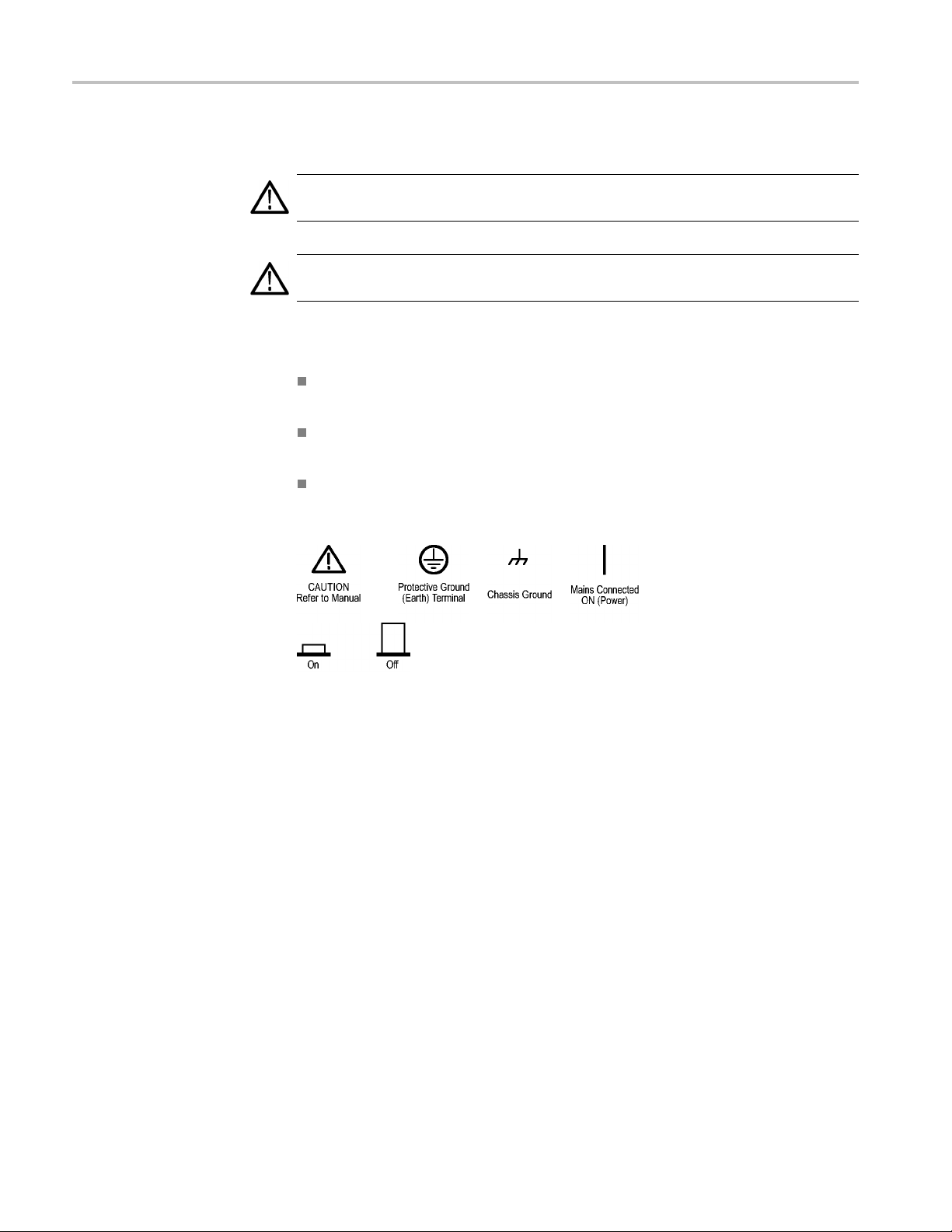
TermsinThisManual
Symbols and Terms on the
Product
These terms may
WARNING. Warning statements identify conditions or practices that could result
in injury or loss of life.
CAUTION. Caution statements identify conditions or practices that could result in
damage to this product or other property.
These terms may appear on the product:
DANGER in
the marking.
WAR NI NG
read the marking.
CAUTIO
The following symbol(s) may appear on the product:
appear in this manual:
dicates an injury hazard immediately accessible as you read
indicates an injury hazard not immediately a ccessible as you
N indicates a hazard to property including the product.
iv MSO4000 and DPO4000 Series Specifications and Performance Verification
Page 9

Specifications
Page 10

Page 11

Specifications
This chapter contains specifications for the DPO4000 and the MSO4000 series
oscilloscopes. All specifications are guaranteed unless noted as "typical."
Typica l spec
Specifications that are marked with the
Ver ification.
All specifications apply to all DPO4000 and MSO4000 models unless noted
otherwise. To meet specifications, two conditions must first be met:
The oscilloscope must have been operating continuously for twenty minutes
within the operating temperature range specified.
You must perform the Signal Path Compensation (SPC) operation described
in the Tektronix 4000 Series Digital Phosphor Oscilloscopes User Manual
prior to evaluating specifications. If the operating temperature changes by
more than 10 °C (18 °F), you must perform the SPC operation again.
Table 1-1: Analog channel input and vertical specifications
Characteristic Description
Number of input
channels
Input coupling
Input resistance
selection
Input impedance,
DC coupled
Maximum input voltage
(50 Ω)
Maximum input voltage
(1 MΩ)
DC Balance
DPO4032, MSO4032 DPO4104, DPO4054, DPO4034, MSO4104,
2 analog, digitized simultaneously 4 analog, digitized simultaneously
DC, AC, or GND
GND coupling approximates ground reference by measuring the CVR output set to GND. The signal being
measured on the BNC is not disconnected from the channel input load.
1MΩ or 50 Ω
DPO4104, MSO4104: Bandwidth is limited to 500 MHz with 1 MΩ impedance selected.
1MΩ ±1% in parallel with 13 pF ±2 pF
50 Ω ±1%
DPO4104, MSO4104: VSWR ≤1.5:1 from DC to 1 GHz, typical
DPO4054, MSO4054: VSWR ≤1.5:1 from DC to 500 MHz, typical
DPO4034, DPO4032, MSO4034, MSO4032: VSWR ≤1.5:1 from DC to 350 MHz, typical
5V
with peaks ≤ ±20 V (DF ≤ 6.25%)
RMS
The m aximum input voltage at the BNC, between the center conductor and shield is 400 V
39.2%), 250 V
The m aximum transient withstand voltage is ±800 V
0.2 div with the input DC 50 Ω coupled and 50 Ω terminated
0.25 div at 2 mV/div with the input DC 50 Ω coupled and 50 Ω terminated
0.5 div at 1 mV/div with the input DC 50 Ω coupled and 50 Ω terminated
0.2 div with the input DC 1 MΩ coupled and 50 Ω terminated
0.3 div at 1 mV/div with the input DC 1 MΩ coupled and 50 Ω terminated
to 130 kHz derated to 2.6 V
RMS
ifications are provided for your convenience but are not guaranteed.
at 500 MHz.
RMS
symbol are checked in Performance
MSO4054, MSO4034
peak
peak
(DF ≤
MSO4000 and DPO4000 Series Specifications and Performance Verification 1–1
Page 12

Specifications
Table 1-1: Analog channel input and vertical specifications (cont.)
Characteristic Description
Delay between
channels, full
bandwidth, typical
Deskew range
Crosstalk (channel
isolation), typical
TekVPI Interface The probe interface allows installing, powering, compensating, and controlling a wide range of probes
Total probe power
Probe power per
channel
Number of digitized
bits
(coarse)
Sensitivity range (fine) 1 mV/div to 5 V/div: <-50% to >+50% of selected setting, 1 MΩ
Sensitivity resolution
(fine), typical
Position range ±5 divisions
Analog bandwidth,
50 Ω
≤100 ps between any two channels with i nput impedance set to 50 Ω, DC coupling
Note: all settings in the instrument can be manually time aligned using the Probe Deskew function from
-100 ns to +100 ns with a resolution of 20 ps.
-100 ns to +100 ns with a resolution of 20 ps
≥100:1 at ≤100 MHz and ≥30:1 at >100 MHz up to the rated bandwidth for any two channels having
equal Volts/Div settings
offering a variety of features.
The interface is available on all front panel inputs including Aux In. Aux In only provides 1 MΩ input
impedance and does not offer 50 Ω as do the other input channels.
DPO4032, DPO4034, DPO4054, MSO4032, MSO4034, MSO4054: 50 W
DPO4104, MSO4104: 50 W with a derating of 0.8 W/°C for ambient temperatures ≥25 °C
Voltage Max Amperage Voltage Tolerance
5V
12 V
8bits
Displayed vertically with 25 digitization levels (DL) per division, 10.24 divisions dynamic range.
"DL" is the abbreviation for "digitization level." A DL is the smallest voltage level change that can be
resolved by an 8-bit A-D Converter. This value is also known as the LSB (least significant bit).
1MΩ 50 ΩSensitivity range
1 mV/div to 10 V/div in a 1-2-5 sequence 1 mV/div to 1 V/div in a 1-2-5 sequence
10 V/div: <-50% to 0%, 1 M Ω
1 mV/div to 500 mV/div: <-50% to >+50% of selected setting, 50 Ω
1 V/div: <-50% to 0% , 50 Ω
Allows continuous adjustment from 1 mV/div to 10 V/div, 1 M Ω
Allows continuous adjustment from 1 mV/div to 1 V/div, 50 Ω
≤1% of current setting
The limits stated below are for ambient temperature of ≤30 °C and the bandwidth selection set to FULL.
Reduce the upper bandwidth frequency by 1% for each °C above 30 °C.
Instrument
DPO4104, MSO4104 DC to 1 GHz DC to 350 MHz DC to 200 MHz
DPO4054, MSO4054 DC to 500 MHz DC to 350 MHz DC to 200 MHz
Instrument
DPO4034, MSO4034 DC to 350 MHz DC to 200 MHz
DPO4032, MSO4032 DC to 350 MHz DC to 200 MHz
50 mA (250 mW) ±5%
2 A (24 W) ±10%
5 mV/div to 1 V/div 2 mV/div to
4.98 mV/div
2 mV/div to 1 V/div 1 mV/div to 1.99 V/div
1 mV/div to
1.99 mV/div
1–2 MSO4000 and DPO4000 Series Specifications and Performance Verification
Page 13

Table 1-1: Analog channel input and vertical specifications (cont.)
Characteristic Description
Analog bandwidth,
1MΩ with P6139A 10X
Probe, typical
Calculated rise time,
typical
Analog bandwidth
selections
Lower frequency limit,
AC coupled, typical
Upper frequency limit,
250 MHz bandwidth
limited, typical
Upper frequency limit,
20 MHz bandwidth
limited, typical
DC gain accuracy
The limits stated below are for ambient temperature of ≤30 °C and the bandwidth selection set to FULL.
Reduce the upper bandwidth frequency by 1% for each °C above 30 °C.
Instrument
DPO4104, MSO4104 DC to 500 MHz DC to 300 MHz DC to 175 MHz
DPO4054, MSO4054 DC to 500 MHz DC to 300 MHz DC to 175 MHz
DPO4034, MSO4034 DC to 350 MHz DC to 300 MHz DC to 175 MHz
DPO4032, MSO4032 DC to 350 MHz DC to 300 MHz DC to 175 MHz
The formula is calculated by measuring -3 dB bandwidth of the oscilloscope. The formula accounts for the
rise time contribution of the oscilloscope independent of the rise time of the signal source.
Instrument
DPO4104, MSO4104
DPO4054, MSO4054
DPO4034, MSO4034
DPO4032, MSO4032
Instrument
DPO4104, MSO4104
DPO4054, MSO4054
DPO4034, MSO4034
DPO4032, MSO4032
20 MHz, 250 MHz and Full (all models)
< 10 Hz when AC to 1 MΩ coupled
The AC coupled lower frequency limits are reduced by a factor of 10 when 10X passive probes are used.
250 MHz, ±20% (all models)
20 MHz, ±20% (all models)
For 1 MΩ path: For 50 Ω path:
±1.5%, derated at 0.100% /°C above 30 °C
±3.0% Variable Gain, derated at 0.100%/°C above
30 °C
50 mV/div to 100 V/div 20 mV/div to
50 Ω : 1 mV/div to
1.99 mV/div
1.75 ns 778 ps 350 ps
1.75 ns 778 ps 700 ps
1.75 ns 1 ns 1 ns
1.75 ns 1 ns 1 ns
1MΩ (P6139A
probe): 10 mV/div
to 19.9 mV/div
1 ns 700 ps
1 ns 700 ps
1ns 1ns
1ns 1ns
Specifications
10 mV/div to
49.8 m V/div
50 Ω : 2 mV/div to
4.99 mV/div
1MΩ (P6139A probe): 20 mV/div to 100 V/div
±1.5%, derated at 0.050% /°C above 30 ° C
±3.0% Variable Gain, derated at 0.050%/°C above
30 °C
19.9 m V/div
50 Ω : 5 mV/div to
1V/div
MSO4000 and DPO4000 Series Specifications and Performance Verification 1–3
Page 14

Specifications
Table 1-1: Analog channel input and vertical specifications (cont.)
Characteristic Description
DC voltage
measurement
accuracy
Sample
acquisition mode,
typical
Average
acquisition mode
Offset ranges
Offset accuracy ±[0.005 × | offset - position | + DC Balance]
Measurement type
Any sample
Delta volts between any two samples acquired
with the same oscilloscope setup and ambient
conditions
Note: Offset, position, and the constant offset term must be converted to volts by multiplying by the
appropriate volts/div term.
Average of ≥ 16 waveforms ±[DC gain accuracy x | reading - (offset - position) |
Delta Volts between any two averages of ≥16
waveforms acquired with the same oscilloscope
setup and ambient conditions
Note: Offset, position, and the constant offset term must be converted to volts by multiplying by the
appropriate volts/div term.
The basic accuracy specification applies directly to any sample and to the following measurements: High,
Low, Max, Min, Mean, Cycle Mean, RMS, and Cycle RMS. The delta volt accuracy specification applies to
subtractive calculations involving two of these measurements.
The delta volts (difference voltage) accuracy specification applies directly to the following measurements:
Positive Overshoot, Negative Overshoot, Pk-Pk, and Amplitude.
1 mV/div to 50 mV/div
50.5 m V/div to 99.5 mV/div
100 mV/div to 500 mV/div
505 mV/div to 995 mV/div
1 V/div to 5 V/div
5.05 V /div to 10 V/div
1
1
Input Signal cannot exceed Max Input Voltage for the 50 Ω input path. Refer to the Max Input Voltage
specification for more information.
Note: Both the position and constant offset term must be converted to volts by multiplying by the
appropriate volts/div term.
DC Accuracy (in volts)
±[DC gain accuracy x | reading - (offset - position) |
+ Offset Accuracy + 0.15 div + 0.6 mV]
±[DC gain accuracy x | reading | + 0.15 div +
1.2 mV]
+ O ffset Accuracy + 0.1 div]
±[DC gain accuracy x | reading | + 0.05 div]
Offset rangeVolts/div setting
1MΩ input 50 Ω input
±1 V ±1 V
±0.5 V ±0.5 V
±10V ±10V
±5 V ±5 V
±100 V ±5 V
±50 V Not applicable
1–4 MSO4000 and DPO4000 Series Specifications and Performance Verification
Page 15

Table 1-1: Analog channel input and vertical specifications (cont.)
Characteristic Description
Random Noise
Sample Acquisition
Mode
Aperture uncertainty
,
Model Bandwidth selection 1 MΩ 50 Ω
DPO4104
Full Bandwidth
250 MHz
20 MHz
DPO4054
Full Bandwidth
250 MHz
20 MHz
DPO4034
Full Bandwidth
250 MHz
20 MHz
DPO4032
Full Bandwidth
250 MHz
20 MHz
≤(3 ps + 0.1 ppm × Record Duration)
, for records having duration ≤1 minute
RMS
RMS Noise
≤(133 µV + 7.3% of
Volts/div Setting)
≤(99.5 µV + 5.0% of
Volts/div Setting)
≤(20.8 µV + 3.3% of
Volts/div Setting)
≤(130 µV + 7.6% of
Volts/div Setting)
≤(96.2 µV + 5.2% of
Volts/div Setting)
≤(22.7 µV + 3.8% of
Volts/div Setting)
≤(139 µV + 6.4% of
Volts/div Setting)
≤(94.0 µV + 4.8% of
Volts/div Setting)
≤(22.3 µV + 3.4% of
Volts/div Setting)
≤(141 µV + 7.2% of
Volts/div Setting)
≤(87.9 µV + 4.9% of
Volts/div Setting)
≤(18.5 µV + 3.1% of
Volts/div Setting)
Specifications
≤(72.3 μV + 6% of
Volts/div Setting)
≤(49.6 µV + 3.7% of
Volts/div Setting)
≤(12.8 µV + 3.3% of
Volts/div Setting)
≤(77.9 μV + 3.1% of
Volts/div Setting)
≤(56.7 µV + 3.3% of
Volts/div Setting)
≤(13.6 µV + 3.3% of
Volts/div Setting)
≤(77.7 µV + 3.3% of
Volts/div Setting)
≤(76.6 µV + 3.2% of
Volts/div Setting)
≤(16.0 µV + 3.1% of
Volts/div Setting)
≤(81.6 µV + 3.1% of
Volts/div Setting)
≤(73.8 µV + 3.9% of
Volts/div Setting)
≤(12.7 µV + 3.6% of
Volts/div Setting)
MSO4000 and DPO4000 Series Specifications and Performance Verification 1–5
Page 16

Specifications
Table 1-1: Analog channel input and vertical specifications (cont.)
Characteristic Description
Delta Time
Measurement
Accuracy
The formula to calculate delta-time measurement accuracy (DTA) for a given instrument setting and input
signal is given below (assumes insignificant signal content above Nyquist)
=SlewRate(1stEdge) around 1stpoint in measurement
SR
1
=SlewRate(2ndEdge) around 2ndpoint in measurement
SR
2
N = input-referred noise (volts
, Refer to Random Noise, Sample Acquisition Mode)
rms
TBA = timebase accuracy (5 ppm, Refer to Long-term sample rate and delay time accuracy)
= delta-time measurement duration (sec)
t
reading
RecordDuration = (Record Length) / (Sample Rate)
Assumes that error due to aliasing is insignificant
The term under the square-root sign is the stability, and is due to TIE (Time Interval Error). The errors due
to this term occur throughout a single-shot measurement. The second term is due to both the absol
center-frequency accuracy and the center-frequency stability of the time base and varies between multiple
single-shot measurements over the observation interval (the amount of time from the first single-shot
measurement to the final single-shot measurement).
1
For 50 Ω path, 1 V/div is the maximum vertical setting.
ute
1–6 MSO4000 and DPO4000 Series Specifications and Performance Verification
Page 17

Specifications
Table 1-2: Digi
tal channel input specifications, MSO4000 only
Characteristic Description
Threshold vol
Digital threshold accuracy
Timing resolution
tage range
-2Vto+5V
±[100 mV + 3% o
f the threshold setting after calibration]
2 ns for the main memory and 60.6 ps for MagniVu memory
Table 1-3: Horizontal and acquisition system specifications
Characteristic
Long-term sample rate and delay
time accuracy
Seconds/Division range
Record Length
1 K 400 ps – 40 s 1 ns – 40 s
10 K 400 ps – 400 s 1 ns – 400 s
100 K
1M
10 M
response, typical
Sample-rate range DPO4104, MSO4104: 5 GS/s-0.1 S/s
Record length range 10 M, 1 M, 100 k, 10 k, 1 k
Maximum update rate
Aperture Uncertainty, typical
Number of Waveforms for Average
Acquisition Mode
Description
±5 ppm over any ≥1mstimeinterval
DPO4104, MSO4104
400 ps – 1,000 s 1 ns – 1,000 s
1-2-4 sequence 1-2-4 sequence except one position in each
Minimum pulse widthPeak Detect or Envelope mode pulse
DPO4104, MSO4104: > 200 ps
DPO4054, DPO4034, DPO4032, MSO4054, MSO4034, MSO4032: > 400 ps
DPO4054, DPO4034, DPO4032, MSO4054, MSO4034, MSO4032: 2.5 GS/s – 0.1 S/s
Maximum triggered acquisition rate: 50,000 wfm/s
≤(3 ps + 0.1 ppm × record duration)
, for records having duration ≤1minute
RMS
2 to 512 waveforms
Default of 16 waveforms
DPO4054, DPO4034, DPO4032,
MSO4054, MSO4034, MSO4032
record length selection, which is 0.8-2-4.
Table 1-4: Trigger specifications
Characteristic Description
Aux In (External) trigger maximum
input voltage
Aux In (External) trigger input
The maximum input voltage at the BNC, between center conductor and shield, is 400 V
(DF ≤39.2% ), 250 V
The maximum transient withstand voltage is ±800 V
to 2 MHz derated to 5 V
RMS
@ 500 MHz.
RMS
peak
.
1MΩ ±1% in parallel with 13 pF ±2 pF
peak
impedance, typical
Aux In (External) trigger bandwidth,
250 MHz ±20%
typical
Trigger bandwidth, Edge, Pulse, and
Logic, typical
DPO4104, MSO4104: 1 GHz
DPO4054, MSO4054: 500 MHz
DPO4034, DP O4032, MSO4034, MSO4032: 350 MHz
Time accuracy for Pulse, Glitch,
Timeout, or Width triggering
Time range Accuracy
1nsto500ns
520 ns to 1 s
±(20% of setting + 0.5 ns)
±(0.01% of setting + 100 ns)
MSO4000 and DPO4000 Series Specifications and Performance Verification 1–7
Page 18

Specifications
Table 1-4: Trigger specifications (cont.)
Characteristic Description
Edge-type trigger sensitivity, DC
coupled, typical
Edge trigger sensitivity, not DC
coupled, typical
Trigger level ranges
Lowest frequency for successful
operation of "Set Level to 50%"
function, typical
Trigger level accuracy, DC coupled
typical
Trigger holdoff range
Video-type trigger sensitivity, typical
Video-type trigger formats and field
rates
Trigger Source Sensitivity
Any input channel
Aux in (External) 200 mV from DC to 50 MHz, increasing to
Line Fixed
Trigger Coupling Typical Sensitivity
NOISE REJ 2.5 times the DC-coupled limits
HF REJ
LF REJ
Source Sensitivity
Any input channel
Aux In (External)
Line Not applicable
The line trigger level is fixed at about 50% of the line voltage.
This specification applies to logic and pulse thresholds.
45 Hz
For signals having rise and fall times ≥10 ns, the limits are as follows:
Source
Any channel ±0.20 divisions
Aux In (external trigger) ±(10% of setting + 25 mV)
Line Not applicable
20 ns minimum to 8 s maximum
The limits for both delayed and main trigger are as follows:
Source Sensitivity
Any input channel
Aux In (External)
Triggers from negative sync composite video, field 1 or field 2 for interlaced systems, on any
field, specific line, or any line for interlaced or non-interlaced systems. Supported systems
include NTSC, PAL, and SECAM.
0.40 div from DC to 50 MHz, increasing to
1 div at oscilloscope bandwidth
500 mV at 250 MHz
1.5 times the DC-coupled limit from DC to
50 kHz. Attenuates signals above 50 kHz
1.5 times the DC-coupled limits for
frequencies above 50 kHz. Attenuates
signals below 50 kHz
±8 divisions from center of screen,
±8 divisions from 0 V when vertical LF reject
trigger coupling is selected
±8 V
Range
0.6 to 2.5 divisions of video sync tip
Video not supported through Aux In
(External) input
1–8 MSO4000 and DPO4000 Series Specifications and Performance Verification
Page 19

Table 1-4: Trigger specifications (cont.)
Characteristic Description
Logic-type or logic qualified trigger
or events-delay sensitivities, DC
coupled, typical
Pulse-type runt trigger sensitivities,
typical
Pulse-type trigger width and glitch
sensitivities, typical
Logic-type triggering, minimum logic
or rearm time, typical
Minimum clock pulse widths for
setup/hold time violation trigger,
typical
Setup/hold violation trigger, setup
and hold time ranges, DPO4000 only
MSO4000 only
1.0 division from DC to maximum bandwidth
1.0 division from DC to maximum bandwidth
1.0 division
For all vertical settings, the minimums are:
Trigger type Minimum pulse
Logic Not applicable 2 ns 1 ns
Time Qualified
Logic
For all vertical settings, the minimums are:
Minimum pulse width, clock active
User hold time + 2.5 ns
Feature Min Max
Setup time
Hold time 4 ns 8 s
Setup + Hold time
Feature Min Max
Setup time
Hold time 1 n s 1.0 ms
Setup + Hold time
Input coupling on clock and data channels must be the same.
For Setup time, positive numbers mean a data transition before the clock.
For Hold time, positive numbers mean a data transition after the clock edge.
Setup + Hold time is the algebraic sum of the Setup Time and the Hold Time programmed by
the user.
width
Minimum re-arm
time
Minimum time
between channels
4ns 2ns 1ns
2
3
Minimum pulse width, clock inactive
2ns
0ns 8s
4ns 16s
-0.5 ns 1.0 ms
0.5 ns 2.0 ms
Specifications
1
2
MSO4000 and DPO4000 Series Specifications and Performance Verification 1–9
Page 20

Specifications
Table 1-4: Trigger specifications (cont.)
Characteristic Description
Pulse type trigger, minimum pulse,
rearm time, minimum transition time
Transition time trigger, delta time
range
Time range for glitch, pulse width,
timeout, time-qualified runt, or
time-qualified window triggering
B trigger after events, minimum
pulse width and maximum event
frequency, typical
B trigger, minimum time between
arm and trigger, typical
B trigger after time, time range
B trigger after events, event range
Maximum serial trigger bits 128 bits
Standard Parallel bus interface
triggering (MSO4000 only)
Pulse class Minimum pulse
Glitch
Runt 4 ns 2 ns
Time-qualified runt
Width 4 ns
Slew rate
For the trigger class width and the trigger class runt, the pulse width refers to the width of the
pulse being measured. The rearm time refers to the time between pulses.
For the trigger class slew rate, the pulse width refers to the delta time being measured. The
rearm time refers to the time it takes the signal to cross the two trigger thresholds again.
4nsto8s
4nsto8s
4 ns, 500 MHz
4ns
For trigger after time, this is the time between the end of the time period and the B trigger
event.
For trigger after events, this is the time between the last A trigger event and the first B trigger
event.
4nsto8seconds
1 to 9,999,999
Data Trigger: 1 to 20 bits of user specified data on 4-channel models and 1 to 18 bits of
user specified data on 2-channel models.
width
4ns
4ns
4ns
Minimum rearm time
2 ns + 5% of glitch width setting
8.5 ns + 5% of width setting
2 ns + 5% of width upper limit setting
8.5 ns + 5% of delta time setting
1–10 MSO4000 and DPO4000 Series Specifications and Performance Verification
Page 21

Table 1-4: Trigger specifications (cont.)
Characteristic Description
Standard serial bus interface triggering
I2C Address Triggering: 7 and 10 bit user specified address, as well as General Call, START
byte, HS-mode, EEPROM, and CBUS
Data Trigger: 1 to 5 bytes of user specified data
Trigger On: Start, Repeated Start, Stop, Missing Ack, Data, or Address and Data
Maximum Data Rate: 10 Mbps
SPI Data Trigger: 1 to 16 bytes of user specified data
Trigger On: SS Active, Start of Frame, MOSI, MISO, or MOSI and MISO
Maximum Data Rate: 10 Mbps
CAN Data Trigger: 1 to 8 bytes of user specified data, including qualifiers of equal to (=), not equal
to (<>), less than (<), greater than (>), less than or equal to (<=), greater than or equal to (>=)
Trigger On: Start of Frame, Type of Frame, Identifier, Data, Identifier and Data, End of Frame,
Missing Ack, or Bit Stuffing Error
Frame Type: Data, Remote, Error, Overload
Identifier: Standard (11 bit) and Extended (29 bit) identifiers
Maximum Data Rate: 1 Mbps
RS-232 Trigger On: Tx Start Bit, Rx Start Bit, Tx End of P a cket, Rx End of Packet, Tx Data, Rx Data,
Tx Parity E rror, or Rx Parity Error
Maximum Data Rate: 10 Mbps
4
LIN
Identifier Trigger: 6 bits of user-specified data, equal to (=)
Data Trigger: 1 to 8 bytes of user-specified data, including qualifiers of equal to (=), not equal
to (<>), less than (<), greater than (>), less than or equal to (<=), greater than or equal to
(>=), inside range, or outside range
Error: Sync, Identifier Parity, Checksum
Trigger On: Sync, Identifier, Data, ID & Data, Wakeup Frame, Sleep Frame, or Error
Maximum Data Rate: 100 kbps
Specifications
MSO4000 and DPO4000 Series Specifications and Performance Verification 1–11
Page 22

Specifications
Table 1-4: Trigger specifications (cont.)
Characteristic Description
FlexRay
I2S
Left Justified
Right Justified
TDM
1
For logic, time between channels refers to the length of time a logic state derived from more than one channel must exist to be recognized. For events, thetime
is the minimum time between a main and delayed event that will be recognized if more than one channel is used.
2
n active pulse width is the width of the clock pulse from its active edge (as defined through the Define Inputs lower-bezel button and the Clock Edge side-bezel
A
menu) to its inactive edge. An inactive pulse width is the width of the pulse from its inactive edge to its active edge.
3
The User hold time is the number selected by the user through the Times lower-bezel button and the Hold Time side-bezel menu.
4
DPO4000 Series: S/N CO20000/B020000 and above; MSO4000 Series: all units.
4
Indicator bits: Normal Frame, Payload Fram e, Null Frame, Sync Frame, Startup Frame
Identifier Trigger: 11 bits of user-specified data, equal to (=), not equal to (<>), less than (<),
greater than (>), less than or equal to (<=), greater than or equal to (>=), Inside Range, or
Outside Range
Cycle Count Trigger: 6 bits of user-specified data, equal to (=)
Header Fields Trigger: 40 bits of user-specified data comprising Indicator Bits, Identifier,
Payload Length, Header CRC, Cycle Count, or equal to (=)
Data Trigger: 1 to 16 Bytes of user-specified data, with 0 to 253, or "don’t care" bytes of data
offset, including qualifiers of equal to (=), not equal to <>, less than (<), greater than (>), less
than or equal to (<=), greater than or equal to (>=), Inside Range, Outside Range
End Of Frame: User-chosen types S tatic, Dynamic (DTS), and All
Error: Header CRC, Trailer CRC, Null Frame-static, Null Frame-dynamic, Sync Frame,
Startup Frame
Trigger On: Start of Frame, Indicator Bits, Identifier, Cycle Count, Header Fields, Data,
Identifier & D ata, End of Frame, or Error
Maximum Data Rate: 10 Mbps
4
Data Trigger: 32 bits of user-specified data in a left word, right word, or either, including
qualifiers of equal to (=), not equal to <>, less than (<), greater than (>), less than or equal to
(<=), greater than or equal to (>=), inside range, outside range
Trigger on: Word Select, Data
Maximum Data Rate: 12.5 Mbps
4
Data Trigger: 32 bits of user-specified data in a channel 0-7, including qualifiers of equal to
(=), not equal to <>, less than (<), greater than (>), less than or equal to (<=), greater than or
equal to (>=), inside range, outside range
Trigger on: Frame Sync, Data
Maximum Data Rate: 25 Mbps
1–12 MSO4000 and DPO4000 Series Specifications and Performance Verification
Page 23

Specifications
Table 1-5: Disp
Characteristic Description
Display type
Display resolution 1000 horizontal by 651 vertical displayed pixels
Luminance, typical
Waveform display color scale The TFT display can support up to 262,144 colors. A subset of these colors are used for the
lay specifications
Display area: 210.4 mm (8.28 inches) (H) x 157.8 mm (6.21 inches) (V), 264 mm
(10.4 inches) diagonal, 6-bit RGB full color, XGA (1024 x 768) TFT liquid crystal display
(LCD).
Minimum 240 cd/m
oscillosc
ope display, all of which are fixed colors and not changeable by the customer.
2
, typical 300 cd/m
2
Table 1-6: Input/Output port specifications
Characteristic Description
Ethernet interface Standard on all models: 10/100 Mbps
USB interface 1 Device and 3 Host connectors (all models)
GPIB interface Available as an optional accessory that connects to USB Device and USB Host port. with
the TEK-USB-488 GPIB to USB Adapter
Control interface is incorporated in the instrument user interface.
Video signal output
Probe compensator output voltage
and frequency, typical
ger (Auxiliary) output (AUX
Trig
OUT)
A 15 pin, XGA RGB-type connector
Output voltage: 0 V to 2.5 V ±1% behind 1 kΩ ±2%
Frequency: 1 kHz ±5%
LOW TRUE; LOW to HIGH transition indicates that the trigger occurred. The logic levels are:
Characteristic
Vout (HI) ≥2.5 V open circuit; ≥1.0 V into a 50 Ω load
Vout (LO) ≤0.7 V into a load of ≤4mA;≤0.25 V into a
Limits
to ground
50 Ω load to ground
able 1-7: Power source specifications
T
Characteristic Description
Source voltage 100 V to 240 V ±10%
Source frequency (90 V to 264 V) 47 Hz to 66 Hz
(100 V to 132 V) 360 Hz to 440 Hz
Fuse rating T6.3AH, 250 V
The fuse is not customer replaceable.
MSO4000 and DPO4000 Series Specifications and Performance Verification 1–13
Page 24

Specifications
Table 1-8: Data
storage specifi cations
Characteristic Description
Nonvolatile m
emory retention time,
No time limit for front-panel settings, saved waveforms, setups, and calibration constants
typical
Real-time cl
Compact Fla
ock
sh card
A programmab
Used to stor
Supply Volt
Switched 3
le clock providing time in years, months, days, hours, minutes, and seconds
e reference waveforms and front-panel settings
age
.3 V only
Form factor
Type 1 only
Table 1-9: Environmental specifications
Characteristic Description
Temperature
Humidity
Altitude
Pollution Degree Pollution Degree 2, indoor use only
Random vibration
Operating: 0 °C to +50 °C (+32 °F to +122 °F)
Nonoperating: -20 °C to +60 °C (-4 °F to +140 °F)
Operating:
High: 10% to 60% relative humidity, 40 °C to 50 °C (104 °F to 122 °F)
Low: 10% to 90% relative humidity, 0 °C to 40 °C (32 °F to 104 °F)
Nonoperating:
High: 5% to 60% relative humidity, 40 °C to 60 °C (104 °F to 140 °F)
Low: 5% to 90% relative humidity, 0 °C to 40 ° C (32 °F to 104 °F)
Operating: 3,000 m (9,843 ft)
Nonoperating: 12,000 m (39,370 ft)
Operating: 0.31 g
Nonoperating: 2.46 g
from 5 Hz to 500 Hz, 10 minutes on each axis, 3 axes
RMS
from 5 Hz to 500 Hz, 10 minutes on each axis, 3 axes (30 minutes
RMS
total).
Data bits
16 bit data
transfer
1–14 MSO4000 and DPO4000 Series Specifications and Performance Verification
Page 25

Specifications
Table 1-10: Mec
Characteristic Description
Dimensions Nominal, non-
Weight
Clearance Requirements The clearance requirement for adequate cooling is:
hanical specifications
Height: 229 mm (9.0 in), including feet: 272 mm (10.7 in), including vertical handle and feet
Width: 439 mm (17.3 in) from handle hub to handle hub
Depth:
137 mm (5.4 in) from feet to front of knobs
145 mm (5.7 in) from feet to front of front cover
Nominal, ra
Height: 218 mm (8.6 in)
Width: 488 mm (19.2 in) from outside of handle to outside of handle
Depth: 559 m
5.1kg(11.
8.7 kg (19.1 lbs), instrument with rackmount, without front cover
9.5 kg (21.0 lbs), when packaged for domestic shipment and without rackmount
50.8 mm (2
rear of the unit
rackmount:
ckmount (5U rack sizes):
m (22.0 in) from outside of handle to back of slide
3 lbs), stand-alone instrument, without front cover
in) on the left side (when looking at the front of the instrument) and on the
MSO4000 and DPO4000 Series Specifications and Performance Verification 1–15
Page 26

Specifications
Table 1-11: P65
Characteristic Description
Number of channels
Threshold ac
Maximum sig
Minimum signal swing 500 mV peak-to-peak
Input resistance
Input capacitance 3.0 pF typical
Temperatu
Altitude
Pollution Degree 2, indoor use only
Humidity
16 Digital Probe specifications
curacy
nal swing
re
16
±(100 mV + 3% of threshold)
6.0 V peak-t
20 kΩ
Operating: 0 °C to +50 °C (+32 °F to +122 °F)
Nonoperating: -55 °C to +75 °C (-67 °F to +167 °F)
Operating: 4,500 m (15,000 ft)
Nonoper
10% to 95% relative humidity
o-peak centered around the threshold voltage
ating: 15,000 m (50,000 ft)
1–16 MSO4000 and DPO4000 Series Specifications and Performance Verification
Page 27

Performance Verification
Page 28

Page 29

Performance Verification
This chapter contains performance verification procedures for the specifications
marked with the
required to c
Description Minim um requirements Exam ples
DC voltage source 3 mV to 4 V, ±0.1% accuracy
Leveled sine wave generator
Time mark generator 80 ms period, ±1 ppm accuracy, rise time
Digital Multimeter (DMM) 0.1% accuracy or better
One 50 Ω BNC cable
50 kHz to 1000 MHz, ±4% amplitude
accuracy
<50ns
Male-to-male connectors Tektronix part number 012-0057-01
omplete these procedures.
You may need additional cables and adapters, depending on the actual test
equipment you use.
These procedures cover all DPO4000 and MSO4000 models. Please disregard
checks that do not apply to the specific model you are
Print the test record on the following pages and use it to record the performance
test results for your oscilloscope.
symbol. The following equipment, or a suitable equivalent, is
Fluke 9500 Oscilloscope Calibrator with a
9510 Output Module
An appropriate B NC-to-0.1 inch pin
adapter between the Fluke 9500 and
P6516 probe
testing.
Upgrade the Firmware
NOTE. Completion of the performance verification procedure does not update
the stored time a nd date of the latest successful adjustment. The date and time
are updated only when the adjustment procedures in the service manual are
successfully completed.
The performance verification procedures verify the performance of your
instrument. They do not adjust your instrument. If your instrument fails any of
the performance verification tests, you should perform the factory adjustment
procedures as described in the Tektronix 4000 Series Service Manual.
For the best functionality, you can upgrade the oscilloscope firmware. To upgrade
the firmware, follow these steps:
1. Open up a Web browser and go to www.tektronix.com/software. Us e the
Software and Firmware Finder to locate the most recent firmware upgrade.
2. Download the latest firmware for your oscilloscope onto your PC.
3. Unzip the files and copy the "firmware.img" file into the root folder of a
USB flash drive.
MSO4000 and DPO4000 Series Specifications and Performance Verification 2–1
Page 30

Performance Verification
4. Poweroffyouro
5. Insert the USB flash drive into a USB Host port on the front or back of the
oscilloscope
6. Power on the oscilloscope. The oscilloscope automatically recognizes the
replacemen
If the instrument does not install the firmware, rerun the procedure. If the
problem con
NOTE. Do not power off the oscilloscope or remove the USB flash drive until the
oscilloscope finishes installing the firmware.
The oscilloscope displays a message when the installation is complete.
7. Power of
8. Power on the oscilloscope.
9. Push the Utility front-panel button.
10. Push the Utility Page lower-bezel button.
11. Turn multipurpose knob a and select Config.
f the oscilloscope and remove the USB flash drive.
scilloscope.
.
t firmware and installs it.
tinues, contact qualified service personnel.
12. Push the About lower-bezel button. The oscilloscope displays the firmware
version number.
13. Confirm that the version number matches that of the new firmware.
2–2 MSO4000 and DPO4000 Series Specifications and Performance Verification
Page 31

Performance Verification
Test Record
Model Serial Procedure performed by Date
Test Passed Failed
Self Test
Input Impedance
Performance checks Vertical scale Low limit Test result High limit
All models:
Channel 1 Input
Impedance, 1 MΩ
Impedance, 50 Ω
Channel 2 Input
Impedance, 1 MΩ
Impedance, 50 Ω
DPO4104, DPO4054, DPO4034, MSO4104, MSO4054, MSO4034:
Channel 3 Input
Impedance, 1 MΩ
Impedance, 50 Ω
Channel 4 Input
Impedance, 1 MΩ
Impedance, 50 Ω
10 mV/div 990 kΩ 1.01 MΩ
100 mV/div 990 kΩ 1.01 MΩ
1 V/div 990 kΩ 1.01 MΩ
10 mV/div 49.5 Ω 50.5 ΩChannel 1 Input
100 mV/div 49.5 Ω 50.5 Ω
10 mV/div 990 kΩ 1.01 MΩ
100 mV/div 990 kΩ 1.01 MΩ
1 V/div 990 kΩ 1.01 MΩ
10 mV/div 49.5 Ω 50.5 ΩChannel 2 Input
100 mV/div 49.5 Ω 50.5 Ω
10 mV/div 990 kΩ 1.01 MΩ
100 mV/div 990 kΩ 1.01 MΩ
1 V/div 990 kΩ 1.01 MΩ
10 mV/div 49.5 Ω 50.5 ΩChannel 3 Input
100 mV/div 49.5 Ω 50.5 Ω
10 mV/div 990 kΩ 1.01 MΩ
100 mV/div 990 kΩ 1.01 MΩ
1 V/div 990 kΩ 1.01 MΩ
10 mV/div 49.5 Ω 50.5 ΩChannel 4, Input
100 mV/div 49.5 Ω 50.5 Ω
DC Balance
Performance checks Vertical scale Low limit Test result High limit
All models:
Channel 1 DC Balance,
50 Ω,20MHzBW
1 mV/div
2 mV/div
100 mV/div
1V/div
-0.5 mV 0.5 mV
-0.5 mV 0.5 mV
-20mV 20mV
-200 mV 200 mV
MSO4000 and DPO4000 Series Specifications and Performance Verification 2–3
Page 32

Performance Verification
DC Balance
Performance checks Vertical scale Low limit Test result High limit
Channel 1 DC Balance,
1MΩ,20MHzBW
Channel 1 DC Balance,
50 Ω, 250 MHz BW
Channel 1 DC Balance,
1MΩ, 250 MHz BW
Channel 1 DC Balance,
50 Ω,FullBW
Channel 1 DC Balance,
1MΩ,FullBW
Channel 2 DC Balance,
50 Ω,20MHzBW
Channel 2 DC Balance,
1MΩ,20MHzBW
Channel 2 DC Balance,
50 Ω, 250 MHz BW
Channel 2 DC Balance,
1MΩ, 250 MHz BW
Channel 2 DC Balance,
50 Ω,FullBW
1 mV/div
100 mV/div
1V/div
1 mV/div
2 mV/div
100 mV/div
1V/div
1 mV/div
100 mV/div
1V/div
1 mV/div
2 mV/div
100 mV/div
1V/div
1 mV/div
100 mV/div
1V/div
1 mV/div
2 mV/div
100 mV/div
1V/div
1 mV/div
100 mV/div
1V/div
1 mV/div
2 mV/div
100 mV/div
1V/div
1 mV/div
100 mV/div
1V/div
1 mV/div
2 mV/div
100 mV/div
1V/div
1
1
1
1
1
-0.3 mV 0.3 mV
-20mV 20mV
-200 mV 200 mV
-0.5 mV 0.5 mV
-0.5 mV 0.5 mV
-20mV 20mV
-200 mV 200 mV
-0.3 mV 0.3 mV
-20mV 20mV
-200 mV 200 mV
V
-0.5 m
-0.5 m
-20 m
-200
3mV
-0.
0mV
-2
00 mV
-2
0.5 mV
-
0.5 mV
-
V
V
mV
0.5 mV
0.5 mV
20 mV
200 m
mV
0.3
mV
20
0mV
20
.5 mV
0
.5 mV
0
-20mV 20mV
-200 mV 200 mV
-0.3 mV 0.3 mV
-20mV 20mV
-200 mV 200 mV
-0.5 mV 0.5 mV
-0.5 mV 0.5 mV
-20mV 20mV
-200 mV 200 mV
-0.3 mV 0.3 mV
-20mV 20mV
-200 mV 200 mV
-0.5 mV 0.5 mV
-0.5 mV 0.5 mV
-20mV 20mV
-200 mV 200 mV
V
2–4 MSO4000 and DPO4000 Series Specifications and Performance Verification
Page 33

Performance Verification
DC Balance
Performance checks Vertical scale Low limit Test result High limit
Channel 2 DC Balance,
1MΩ,FullBW
1mV/div
100 mV/div
1
1V/div
DPO4104, DPO4054, DPO4034, MSO4104, MSO 4054, MSO4034:
Channel 3 DC Balance,
50 Ω,20MHzBW
1 mV/div
2 mV/div
100 mV/div
1V/div
Channel 3 DC Balance,
1MΩ,20MHzBW
1mV/div
100 mV/div
1
1V/div
Channel 3 DC Balance,
50 Ω, 250 MHz BW
1 mV/div
2 mV/div
100 mV/div
1V/div
Channel 3 DC Balance,
1MΩ, 250 MHz BW
1mV/div
100 mV/div
1
1V/div
Channel 3 DC Balance,
50 Ω,FullBW
1 mV/div
2 mV/div
100 mV/div
1V/div
Channel 3 DC Balance,
1MΩ,FullBW
1mV/div
100 mV/div
1
1V/div
Channel 4 DC Balance,
50 Ω,20MHzBW
1 mV/div
2 mV/div
100 mV/div
1V/div
Channel 4 DC Balance,
1MΩ,20MHzBW
1mV/div
100 mV/div
1
1V/div
Channel 4 DC Balance,
50 Ω, 250 MHz BW
1 mV/div
2 mV/div
100 mV/div
1V/div
-0.3 mV 0.3 mV
-20mV 20mV
-200 mV 200 mV
-0.5 mV 0.5 mV
-0.5 mV 0.5 mV
-20mV 20mV
-200 mV 200 mV
-0.3 mV 0.3 mV
-20mV 20mV
V
-200 m
-0.5 m
mV
-0.5
-20 m
0mV
-20
.3 mV
-0
0mV
-2
200 mV
-
0.5 mV
-
V
V
200 mV
0.5 mV
0.5 m
20 mV
mV
200
3mV
0.
mV
20
00 mV
2
.5 mV
0
V
-0.5 mV 0.5 mV
-20mV 20mV
-200 mV 200 mV
-0.3 mV 0.3 mV
-20mV 20mV
-200 mV 200 mV
-0.5 mV 0.5 mV
-0.5 mV 0.5 mV
-20mV 20mV
-200 mV 200 mV
-0.3 mV 0.3 mV
-20mV 20mV
-200 mV 200 mV
-0.5 mV 0.5 mV
-0.5 mV 0.5 mV
-20mV 20mV
-200 mV 200 mV
MSO4000 and DPO4000 Series Specifications and Performance Verification 2–5
Page 34

Performance Verification
DC Balance
Performance checks Vertical scale Low limit Test result High limit
Channel 4 DC Balance,
1MΩ, 250 MHz BW
1 mV/div
100 mV/div
1
1V/div
Channel 4 DC Balance,
50 Ω,FullBW
1 mV/div
2 mV/div
100 mV/div
1V/div
Channel 4 DC Balance,
1MΩ,FullBW
1 mV/div
100 mV/div
1
1V/div
1
Immediately after calibration, the specification is -0.2 div to 0.20 div.
Performance checks: Bandwidth
Bandwidth at
Channel Impedance Vertical scale V
All models:
1
1
1
1
1
1
2
2
2
2
2
2
50 Ω 5 m V/div
50 Ω 2 m V/div
50 Ω 1 m V/div
1MΩ 5 mV/div
1MΩ 2 mV/div
1MΩ 1 mV/div
50 Ω 5 m V/div
50 Ω 2 m V/div
50 Ω 1 m V/div
1MΩ 5 mV/div
1MΩ 2 mV/div
1MΩ 1 mV/div
DPO4104, DPO4054, D PO4034, MSO4104, MSO4054, MSO4034:
3
3
3
3
3
3
4
50 Ω 5 m V/div
50 Ω 2 m V/div
50 Ω 1 m V/div
1MΩ 5 mV/div
1MΩ 2 mV/div
1MΩ 1 mV/div
50 Ω 5 m V/div
-0.3 mV 0.3 mV
-20mV 20mV
-200 mV 200 mV
-0.5 mV 0.5 mV
-0.5 mV 0.5 mV
-20mV 20mV
-200 mV 200 mV
-0.3 mV 0.3 mV
-20mV 20mV
-200 mV 200 mV
For performance verification testing, the specification is -0.3 to 0.3 div.
in-pp
V
bw-pp
Limit
≥ 0.707
≥ 0.707
≥ 0.707
≥ 0.707
≥ 0.707
≥ 0.707
≥ 0.707
≥ 0.707
≥ 0.707
≥ 0.707
≥ 0.707
≥ 0.707
≥ 0.707
≥ 0.707
≥ 0.707
≥ 0.707
≥ 0.707
≥ 0.707
≥ 0.707
Test result
Gain =
V
bw-pp/Vin-pp
2–6 MSO4000 and DPO4000 Series Specifications and Performance Verification
Page 35

Performance Verification
Performance checks: Bandwidth
Test result
Bandwidth at
Channel Impedance Vertical scale V
4
4
4
4
4
50 Ω 2 m V/div
50 Ω 1 m V/div
1MΩ 5 mV/div
1MΩ 2 mV/div
1MΩ 1 mV/div
in-pp
V
bw-pp
Limit
≥ 0.707
≥ 0.707
≥ 0.707
≥ 0.707
≥ 0.707
DC Gain Accuracy
Performance checks Vertical scale Low limit Test result High limit
All models:
Channel 1 DC Gain
Accuracy, 0 V offset,
ical position,
0Vvert
20 MHz BW, 50 Ω
1 mV/div -1.5% 1.5%
2 mV/div -1.5% 1.5%
4.98 mV
-3.0% 3.0%
5 mV/div -1.5% 1.5%
10 m V/div -1.5% 1.5%
20 m V/div -1.5% 1.5%
8mV
49.
-3.0% 3.0%
50 m V/div -1.5% 1.5%
100 m V /div -1.5% 1.5%
200 m V /div -1.5% 1.5%
500 m V /div -1.5% 1.5%
1.0 V/div -1.5% 1.5%
Channel 1 DC Gain
Accuracy, 0 V offset,
0 V vertical position,
20 MHz BW, 1 MΩ
1 mV/div -1.5% 1.5%
2 mV/div -1.5% 1.5%
4.98 m V /div -3.0% 3.0%
5 mV/div -1.5% 1.5%
10 m V/div -1.5% 1.5%
20 m V/div -1.5% 1.5%
49.8 mV
-3.0% 3.0%
50 m V/div -1.5% 1.5%
100 m V /div -1.5% 1.5%
200 m V /div -1.5% 1.5%
500 m V /div -1.5% 1.5%
1 V/div -1.5% 1.5%
Gain =
V
bw-pp/Vin-pp
MSO4000 and DPO4000 Series Specifications and Performance Verification 2–7
Page 36

Performance Verification
DC Gain Accuracy
Performance checks Vertical scale Low lim it Test result High limit
Channel 2 DC Gain
Accuracy, 0 V offset,
0Vverticalp
20 MHz BW, 50 Ω
Channel 2 DC Gain
Accuracy, 0 V offset,
0Vv
20 MHz BW, 1 M Ω
DPO4104, DPO4054, D PO4034, MSO4104, MSO4054, MSO4034:
Channel 3 DC Gain
Accuracy, 0 V offset,
0 V vertical position,
20 MHz BW, 50 Ω
osition,
ertical position,
1 mV/div -1.5% 1.5%
2 mV/div -1.5% 1.5%
4.98 mV
5 mV/div -1.5% 1.5%
10 mV/div -1.5% 1.5%
20 mV/div -1.5% 1.5%
49.8 mV
50 mV/div -1.5% 1.5%
100 m V/div -1.5% 1.5%
200 m V/div -1.5% 1.5%
500 m V/div -1.5% 1.5%
1.0 V/div -1.5% 1.5%
1 mV/div -1.5% 1.5%
2 mV/div -1.5% 1.5%
4.98 m V/div -3.0% 3.0%
5 mV/div -1.5% 1.5%
10 mV/div -1.5% 1.5%
20 mV/div -1.5% 1.5%
9.8 mV
4
50 mV/div -1.5% 1.5%
100 m V/div -1.5% 1.5%
200 m V/div -1.5% 1.5%
500 m V/div -1.5% 1.5%
1 V/div -1.5% 1.5%
1 mV/div -1.5% 1.5%
2 mV/div -1.5% 1.5%
4.98 mV
5 mV/div -1.5% 1.5%
10 mV/div -1.5% 1.5%
20 mV/div -1.5% 1.5%
49.8 mV
50 mV/div -1.5% 1.5%
100 m V/div -1.5% 1.5%
200 m V/div -1.5% 1.5%
500 m V/div -1.5% 1.5%
1.0 V/div -1.5% 1.5%
-3.0% 3.0%
-3.0% 3.0%
-3.0% 3.0%
-3.0% 3.0%
-3.0% 3.0%
2–8 MSO4000 and DPO4000 Series Specifications and Performance Verification
Page 37

Performance Verification
DC Gain Accuracy
Performance checks Vertical scale Low limit Test result High limit
Channel 3 DC Gain
Accuracy, 0 V offset,
0Vverticalp
20 MHz BW, 1 MΩ
Channel 4 DC Gain
Accuracy, 0 V offset,
0Vv
20 MHz BW, 50 Ω
Channel 4 DC Gain
Accuracy, 0 V offset,
0 V vertical position,
20 MHz BW, 1 MΩ
osition,
ertical position,
1 mV/div -1.5% 1.5%
2 mV/div -1.5% 1.5%
4.98 m V /div -3.0% 3.0%
5 mV/div -1.5% 1.5%
10 m V/div -1.5% 1.5%
20 m V/div -1.5% 1.5%
49.8 mV
50 m V/div -1.5% 1.5%
100 m V /div -1.5% 1.5%
200 m V /div -1.5% 1.5%
500 m V /div -1.5% 1.5%
1 V/div -1.5% 1.5%
1 mV/div -1.5% 1.5%
2 mV/div -1.5% 1.5%
8mV
4.9
5 mV/div -1.5% 1.5%
10 m V/div -1.5% 1.5%
20 m V/div -1.5% 1.5%
9.8 mV
4
50 m V/div -1.5% 1.5%
100 m V /div -1.5% 1.5%
200 m V /div -1.5% 1.5%
500 m V /div -1.5% 1.5%
1.0 V/div -1.5% 1.5%
1 mV/div -1.5% 1.5%
2 mV/div -1.5% 1.5%
4.98 m V /div -3.0% 3.0%
5 mV/div -1.5% 1.5%
10 m V/div -1.5% 1.5%
20 m V/div -1.5% 1.5%
49.8 mV
50 m V/div -1.5% 1.5%
100 m V /div -1.5% 1.5%
200 m V /div -1.5% 1.5%
500 m V /div -1.5% 1.5%
1 V/div -1.5% 1.5%
-3.0% 3.0%
-3.0% 3.0%
-3.0% 3.0%
-3.0% 3.0%
MSO4000 and DPO4000 Series Specifications and Performance Verification 2–9
Page 38

Performance Verification
DC Offset Accuracy
Performance
checks Vertical scal
All models:
Channel 1 DC Offset
Accuracy,
20 MHz BW, 50 Ω
Channel 1 DC Offset
Accuracy,
20 MHz BW, 1 MΩ
Channel 2 DC Offset
y,
Accurac
20 MHz BW, 50 Ω
Channel 2 DC Offset
acy,
Accur
20 MHz BW, 1 MΩ
1mV/div
1mV/div
2mV/div
2mV/div
10 mV/div
10 mV/div
100 mV/div
100 mV/div
1mV/div
1mV/div
2mV/div
2mV/div
10 mV/div
10 mV/div
100 mV/div
100 mV/div
1.01 V/div
1.01 V/div
1mV/div
1mV/div
2mV/div
2mV/div
10 mV/div
10 mV/div
100 mV/div
100 mV/div
1mV/div
1mV/div
2mV/div
2mV/div
10 mV/div
10 mV/div
100 mV/div
100 mV/div
1.01 V/div
1.01 V/div
e
Vertical offs
1
et
Low limit Test result
High limit
900 mV 895.0 mV 905.0 mV
-900 mV -905.0 m V -895.0 m V
500 mV 497.0 mV 503.0 mV
-500 mV -503.0 m V -497.0 m V
500 mV 495.5 mV 504.5 mV
-500 mV -504.5 m V -495 mV
5.0 V 4.955 V 5.045 V
-5.0 V -5.045 V -4.955 V
900 mV 895.2 mV 904.8 mV
-900 mV -904.8 m V -895.2 m V
500 mV 497.1 mV 502.9 mV
-500 mV -502.9 m V -497.1 m V
500 mV 495.5 mV 504.5 mV
-500 mV -504.5 m V -495.5 m V
5.0 V 4.955 V 5.045 V
-5.0 V -5.045 V -4.955 V
99.5 V 98.80 V 100.2 V
-99.5 V -100.2 V -98.80 V
900 mV 895.0 mV 905.0 mV
-900 mV -905.0 m V -895.0 m V
500 mV 497.0 mV 503.0 mV
-500 mV -503.0 m V -497.0 m V
500 mV 495.5 mV 504.5 mV
-500 mV -504.5 m V -495.5 m V
5.0 V 4.955 V 5.045 V
-5.0 V -5.045 V -4.955 V
900 mV 895.2 mV 904.8 mV
-900 mV -904.8 m V -895.2 m V
500 mV 497.1 mV 502.9 mV
-500 mV -502.9 m V -497.1 m V
500 mV 495.5 mV 504.5 mV
-500 mV -504.5 m V -495.5 m V
5.0 V 4.955 V 5.045 V
-5.0 V -5.045 V -4.955 V
99.5 V 98.80 V 100.2 V
-99.5 V -100.2 V -98.80 V
2–10 MSO4000 and DPO4000 Series Specifications and Performance Verification
Page 39

DC Offset Accuracy
Performance
checks Vertical scal
e
Vertical offs
1
et
DPO4104, DPO4054, DPO4034, MSO4104, MSO 4054, MSO4034:
Channel 3 DC Offset
Accuracy,
20 MHz BW, 50 Ω
Channel 3 DC Offset
Accuracy,
20 MHz BW, 1 MΩ
Channel 4 DC Offset
y,
Accurac
20 MHz BW, 50 Ω
1 mV/div
1 mV/div
2 mV/div
2 mV/div
10 mV/div
10 mV/div
100 mV/div
100 mV/div
1 mV/div
1 mV/div
2 mV/div
2 mV/div
10 mV/div
10 mV/div
100 mV/div
100 mV/div
1.01 V/div
1.01 V/div
1 mV/div
1 mV/div
2 mV/div
2 mV/div
10 mV/div
10 mV/div
100 mV/div
100 mV/div
900 mV 895.0 mV 905.0 mV
-900 mV -905.0 mV -895.0 mV
500 mV 497.0 mV 503.0 mV
-500 mV -503.0 mV -497.0 mV
500 mV 495.5 mV 504.5 mV
-500 mV -504.5 mV -495.5 mV
5.0 V 4.955 V 5.045 V
-5.0 V -5.04.5 V -4.955 V
900 mV 895.2 mV 904.8 mV
-900 mV -904.8 mV -895.2 mV
500 mV 497.1 mV 502.9 mV
-500 mV -502.9 mV -497.1 mV
500 mV 495.5 mV 504.5 mV
-500 mV -504.5 mV -495.5 mV
5.0 V 4.955 V 5.045 V
-5.0 V -5.045 V -4.955 V
99.5 V 98.80 V 100.2 V
-99.5 V -100.2 V -98.80 V
900 mV 895.0 mV 905.0 mV
-900 mV -905.0 mV -895.0 mV
500 mV 497.0 mV 503.0 mV
-500 mV -503.0 mV -497.0 mV
500 mV 495.5 mV 504.5 mV
-500 mV -504.5 mV -495.5 mV
5.0 V 4.955 V 5.045 V
-5.0 V -5.045 V -4.955 V
Low limit Test result
Performance Verification
High limit
MSO4000 and DPO4000 Series Specifications and Performance Verification 2–11
Page 40

Performance Verification
DC Offset Accuracy
Performance
checks Vertical scal
Channel 4 DC Offset
Accuracy,
20 MHz BW, 1 MΩ
1mV/div
1mV/div
2mV/div
2mV/div
10 mV/div
10 mV/div
100 mV/div
100 mV/div
1.01 V/div
1.01 V/div
1
Use this value for both the calibrator output and the oscilloscope offset setting.
e
Vertical offs
900 mV 895.2 mV 904.8 mV
-900 mV -904.8 m V -895.2 m V
500 mV 497.1 mV 502.9 mV
-500 mV -502.9 m V -497.5 m V
500 mV 495.5 mV 504.5 mV
-500 mV -504.5 m V -495.1 m V
5.0 V 4.955 V 5.045 V
-5.0 V -5.045 V -4.955 V
99.5 V 98.80 V 100.2 V
-99.5 V -100.2 V -98.80 V
Performance checks Low limit Test result High limit
Sample Rate and Delay Time Accuracy
Auxiliary (Trigger) Output
Trigger Output
High 1 MΩ
Low 1 MΩ
Trigger Output
High 50 Ω
Low 50 Ω
1
et
Low limit Test result
High limit
-1 divisions +1 divisions
≥ 2.5 V
–
≥ 1.0 V
–
–
≤ 0.7 V
–
≤ 0.25 V
Random Noise, Sample Acquisition Mode
Vertical sensitivity = 100 mV/div
Performance checks 1 MΩ 50 Ω
Bandwidth Test result (mV) High lim it (mV) Test result (mV) High limit (mV)
DPO4104/MSO4104
Channel 1
Full 7.43 6.07
250 M H z 5.10 3.75
20 MHz 3.32 3.31
Channel 2
Full 7.43 6.07
250 M H z 5.10 3.75
20 MHz 3.32 3.31
Channel 3
Full 7.43 6.07
250 M H z 5.10 3.75
20 MHz 3.32 3.31
Channel 4
Full 7.43 6.07
250 M H z 5.10 3.75
20 MHz 3.32 3.31
2–12 MSO4000 and DPO4000 Series Specifications and Performance Verification
Page 41

Performance Verification
Random Noise, Sample Acquisition Mode
Vertical sensitivity = 100 mV/div
Performance checks 1 MΩ 50 Ω
Bandwidth Test result (mV) High limit (m V) Test result (mV) High limit (mV)
DPO4054/MSO4054
Channel 1
Channel 2
Channel 3
Channel 4
DPO4034/MSO4034
Channel 1
Channel 2
Channel 3
Channel 4
DPO4032/MSO4032
Channel 1
Channel 2
Full 7.73 3.18
250 M Hz 5.30 3.36
20 M H z 3.82 3.31
Full 7.73 3.18
250 M Hz 5.30 3.36
20 M H z 3.82 3.31
Full 7.73 3.18
250 M Hz 5.30 3.36
20 M H z 3.82 3.31
Full 7.73 3.18
250 M Hz 5.30 3.36
20 M H z 3.82 3.31
Full 6.54 3.38
250 M Hz 4.89 3.28
20 M H z 3.42 3.11
Full 6.54 3.38
250 M Hz 4.89 3.28
20 M H z 3.42 3.12
l
Ful
250 M Hz 4.89 3.28
20 M H z 3.42 3.12
ll
Fu
250 M Hz 4.89 3.28
20 M H z 3.42 3.12
Full 7.34 3.18
250 M Hz 4.99 3.97
20 M H z 3.12 3.61
Full 7.3 3.18
250 M Hz 4.99 3.97
20 M H z 3.12 3.61
6.5
6.
4
54
3.3
3.
8
38
MSO4000 and DPO4000 Series Specifications and Performance Verification 2–13
Page 42

Performance Verification
Delta Time Measurement Accuracy
Channel 1
MSO/DPO = 4 ns/Div, Source freq = 240 MHz
MSO/DPO V/Div Source V
5mV 40mV
100 mV 800 mV 46 ps
500 mV 4 V 45 ps
1 V 4 V 86 ps
pp
MSO/DPO = 40 ns/Div, Source freq = 24 MHz
1 mV 8 mV 940 ps
5 mV 40 mV 530 ps
100 mV 800 mV 430 ps
500 mV 4 V 430 ps
1 V 4 V 850 ps
MSO/DPO = 400 ns/Div, Source freq = 2.4 MHz
1mV 8mV 9.4ns
5mV 40mV 5.3ns
100 mV 800 mV 4.3 ns
500 mV 4 V 4.3 ns
1V 4V 8.5ns
MSO/DPO = 4 μs/Div, Source freq = 240 kHz
1 mV 8 mV 94 ns
5mV 40mV 53ns
100 mV 800 mV 43 ns
500 mV 4 V 43 ns
1 V 4 V 85 ns
MSO/DPO = 40 μs/Div, Source freq = 24 kHz
1 mV 8 mV 940 ns
5 mV 40 mV 530 ns
100 mV 800 mV 430 ns
500 mV 4 V 430 ns
1 V 4 V 850 ns
MSO/DPO = 400 μs/Div, Source freq = 2.4 kHz
1mV 8mV 9.4μs
5mV 40mV 5.3μs
100 mV 800 mV 4.3 μs
500 mV 4 V 4.3 μs
1V 4V 8.5μs
Test result High limit
55 ps
2–14 MSO4000 and DPO4000 Series Specifications and Performance Verification
Page 43

Delta Time Measurement Accuracy
Channel 2
MSO/DPO = 4 ns/Div, Source freq = 240 MHz
MSO/DPO V/Div Source V
5mV 40mV
100 mV 800 mV 46 ps
500 mV 4 V 45 ps
1 V 4 V 86 ps
pp
Test result High limit
MSO/DPO = 40 ns/Div, Source freq = 24 MHz
1 mV 8 mV 940 ps
5 mV 40 mV 530 ps
100 mV 800 mV 430 ps
500 mV 4 V 430 ps
1 V 4 V 850 ps
MSO/DPO = 400 ns/Div, Source freq = 2.4 MHz
1mV 8mV 9.4ns
5mV 40mV 5.3ns
100 mV 800 mV 4.3 ns
500 mV 4 V 4.3 ns
1V 4V 8.5ns
MSO/DPO = 4 μs/Div, Source freq = 240 kHz
1 mV 8 mV 94 ns
5mV 40mV 53ns
100 mV 800 mV 43 ns
500 mV 4 V 43 ns
1 V 4 V 85 ns
MSO/DPO = 40 μs/Div, Source freq = 24 kHz
1 mV 8 mV 940 ns
5 mV 40 mV 530 ns
100 mV 800 mV 430 ns
500 mV 4 V 430 ns
1 V 4 V 850 ns
MSO/DPO = 400 μs/Div, Source freq = 2.4 kHz
1mV 8mV 9.4μs
5mV 40mV 5.3μs
100 mV 800 mV 4.3 μs
500 mV 4 V 4.3 μs
1V 4V 8.5μs
Performance Verification
55 ps
MSO4000 and DPO4000 Series Specifications and Performance Verification 2–15
Page 44

Performance Verification
Delta Time Measurement Accuracy
Channel 3
1
MSO/DPO = 4 ns/Div, Source freq = 240 MHz
MSO/DPO V/Div Source V
5mV 40mV
100 mV 800 mV 46 ps
500 mV 4 V 45 ps
1 V 4 V 86 ps
pp
Test result High limit
MSO/DPO = 40 ns/Div, Source freq = 24 MHz
1 mV 8 mV 940 ps
5 mV 40 mV 530 ps
100 mV 800 mV 430 ps
500 mV 4 V 430 ps
1 V 4 V 850 ps
MSO/DPO = 400 ns/Div, Source freq = 2.4 MHz
1mV 8mV 9.4ns
5mV 40mV 5.3ns
100 mV 800 mV 4.3 ns
500 mV 4 V 4.3 ns
1V 4V 8.5ns
MSO/DPO = 4 μs/Div, Source freq = 240 kHz
1 mV 8 mV 94 ns
5mV 40mV 53ns
100 mV 800 mV 43 ns
500 mV 4 V 43 ns
1 V 4 V 85 ns
MSO/DPO = 40 μs/Div, Source freq = 24 kHz
1 mV 8 mV 940 ns
5 mV 40 mV 530 ns
100 mV 800 mV 430 ns
500 mV 4 V 430 ns
1 V 4 V 850 ns
MSO/DPO = 400 μs/Div, Source freq = 2.4 kHz
1mV 8mV 9.4μs
5mV 40mV 5.3μs
100 mV 800 mV 4.3 μs
500 mV 4 V 4.3 μs
1V 4V 8.5μs
55 ps
2–16 MSO4000 and DPO4000 Series Specifications and Performance Verification
Page 45

Performance Verification
Delta Time Measurement Accuracy
Channel 4
1
MSO/DPO = 4 ns/Div, Source freq = 240 MHz
MSO/DPO V/Div Source V
5mV 40mV
100 mV 800 mV 46 ps
500 mV 4 V 45 ps
1 V 4 V 86 ps
pp
Test result High limit
MSO/DPO = 40 ns/Div, Source freq = 24 MHz
1 mV 8 mV 940 ps
5 mV 40 mV 530 ps
100 mV 800 mV 430 ps
500 mV 4 V 430 ps
1 V 4 V 850 ps
MSO/DPO = 400 ns/Div, Source freq = 2.4 MHz
1mV 8mV 9.4ns
5mV 40mV 5.3ns
100 mV 800 mV 4.3 ns
500 mV 4 V 4.3 ns
1V 4V 8.5ns
MSO/DPO = 4 μs/Div, Source freq = 240 kHz
1 mV 8 mV 94 ns
5mV 40mV 53ns
100 mV 800 mV 43 ns
500 mV 4 V 43 ns
1 V 4 V 85 ns
MSO/DPO = 40 μs/Div, Source freq = 24 kHz
1 mV 8 mV 940 ns
5 mV 40 mV 530 ns
100 mV 800 mV 430 ns
500 mV 4 V 430 ns
1 V 4 V 850 ns
MSO/DPO = 400 μs/Div, Source freq = 2.4 kHz
1mV 8mV 9.4μs
5mV 40mV 5.3μs
100 mV 800 mV 4.3 μs
500 mV 4 V 4.3 μs
1V 4V 8.5μs
1
Channels 3 and 4 are only on four channel oscilloscopes.
55 ps
MSO4000 and DPO4000 Series Specifications and Performance Verification 2–17
Page 46

Performance Verification
Performance checks: Digital Threshold Accuracy, MSO4000 series only
Digital
channel Threshold V V Low lim it Test result High limit
0 V -0.1 V 0.1 VD0
4 V 3.78 V 4.22 V
0 V -0.1 V 0.1 VD1
4 V 3.78 V 4.22 V
0 V -0.1 V 0.1 VD2
4 V 3.78 V 4.22 V
0 V -0.1 V 0.1 VD3
4 V 3.78 V 4.22 V
0 V -0.1 V 0.1 VD4
4 V 3.78 V 4.22 V
0 V -0.1 V 0.1 VD5
4 V 3.78 V 4.22 V
0 V -0.1 V 0.1 VD6
4 V 3.78 V 4.22 V
0 V -0.1 V 0.1 VD7
4 V 3.78 V 4.22 V
0 V -0.1 V 0.1 VD8
4 V 3.78 V 4.22 V
0 V -0.1 V 0.1 VD9
4 V 3.78 V 4.22 V
0 V -0.1 V 0.1 VD10
D12
15
D
78 V
0.1 V
-
V
1V
4 V 3.78
0 V -0.1 V 0.1 VD11
4 V 3.78 V 4.22 V
0V -0.
4 V 3.78 V 4.22 V
0 V -0.1 V 0.1 VD13
4V 3.
0 V -0.1 V 0.1 VD14
4 V 3.78 V 4.22 V
V
0
4 V 3.78 V 4.22 V
4.22
0.1
22 V
4.
.1 V
0
V
V
2–18 MSO4000 and DPO4000 Series Specifications and Performance Verification
Page 47

Performance Verification
Performance V
erification Procedures
The following three conditions must be met prior to performing these procedures:
1. The oscillosc ope must have been operating continuously for t wenty (20)
minutes in an environment that meets the operating range specifications for
temperature and humidity.
2. You must perform a signal path compensation (SPC). See Signal Path
Compensation in the Tektronix 4000 Series Digital Phosphor Oscilloscopes
User Manua
(18 °F), you must perform the signal path compensation again.
3. You mus t c
power circuit. Connect the oscilloscope and test instruments into a common
power strip if you are unsure of the AC power circuit distribution. Connecting
the oscilloscope and test instruments into separate AC power circuits can
result in offset voltage s between the equipment, which can invalidate the
performance verification procedure.
The time required to complete the entire procedure is approximately one hour.
WAR N ING. Some procedures use hazardous voltages. To prevent electrical
k, always set voltage source outputs to 0 V before making or changing any
shoc
interconnections.
l. If the operating temperature changes by more than 10 °C
onnect the oscilloscope and the test equipment to the same AC
Sel
fTest
This procedure uses internal routines to verify that the oscilloscope functions and
passes its internal self tests. No test equipment or hookups are required. Start
the self test with these steps:
1. Disconnect all probes and cables from the oscilloscope inputs.
2. Push the front-panel Default Setup button to set the instrument to the factory
default settings.
3. Push the Utility menu button.
4. Push the Utility Page lower-bezel button, and turn the Multipurpose a knob
to select Self Test.
5. Push the Self Test lower-bezel button. The Loop X Times side-bezel menu
will be set to Loop 1 Times.
6. Push the OK Run Self Test side-bezel button.
7. Wait while the self test runs. When the self test completes, a dialog box
displays the results of the self test.
8. Push the Menu Off button to clear the dialog box and Self Test menu.
MSO4000 and DPO4000 Series Specifications and Performance Verification 2–19
Page 48

Performance Verification
Check Input Impedance
(Resistance)
This test check
1. Connect the output of the oscilloscope calibrator (for example, Fluke 9500) to
the oscillosc
2. Push the front-panel Default S etup button to set the instrument to the factory
default settings.
3. Push the front-panel channel button for the oscilloscope channel that you are
testing, as shown in the test record (for example, 1,2,3,4).
4. Confirm that the oscilloscope and calibrator impedances are both set to
1MΩ.The default Impedance setting is 1 MΩ.
s the Input Impedance.
ope channel 1 input, as shown below.
5. Turn the Vertical Scale knob to set the vertical scale, as shown in the test
record (for example, 10 mV/div, 100 mV/div, 1 V/div).
6. Measure the input resistance of the oscilloscope with the calibrator. Record
this value in the test record.
7. Repeat steps 5 and 6 for each volt/division setting in the test record.
8. Change the oscilloscope and calibrator impedance to 50 Ω and repeat steps 5
through 7.
9. Repeat steps 4 through 8 for each channel listed in the test record and relevant
to the model of oscilloscope that you are testing, as shown in the test record
(forexample,2,3,or4).
2–20 MSO4000 and DPO4000 Series Specifications and Performance Verification
Page 49

Performance Verification
Check DC Balance
This test check
You do not need to connect the oscilloscope to any equipment to run this test.
1. Attach a 50 Ω terminator to the channel input of the oscilloscope being tested.
2. Push the fr
default settings.
3. Push the f
testing, as shown in the test record (for example, 1,2,3,4).
4. Set the o
button to select 50 Ω.
5. Push th
side-bezel button for 20MHz, 250MHz,orFull, as given in the test record.
s the DC balance.
ont-panel Default Setup button to set the instrument to the factory
ront-panel channel button for the oscilloscope channel that you are
scilloscope impedance to 50 Ω.PushtheImpedance lower-bezel
e lower-bezel Bandwidth button and push the appropriate bandwidth
6. Turn t
7. Turn the Vertical Scale knob to set the vertical scale, as shown in the test
8. Push the front-panel Acquire button.
9. Push the Mode lower-bezel button, and then, if needed, push the Average
10. If needed, adjust the number of averages to 16 with the Multipurpose a knob.
11. Push the Trigger Menu front-panel button.
12. Push the Source lower-bezel button.
13. Select the AC Line trigger source with the Multipurpose a knob. You do not
14. Push the front-panel Wave Inspector Measure button.
15. Push the Add Measurement lower bezel button.
16. Use the Multipurpose a knob to select the Mean measurement.
he Horizontal Scale knob to 1 ms/division.
rd (for example, 1 mV/div, 2 mV/div, 100 mV/div, 1 V/div).
reco
side bezel button.
need to connect a n external signal to the oscilloscope for this DC Balance test.
MSO4000 and DPO4000 Series Specifications and Performance Verifi
cation 2–21
Page 50

Performance Verification
Check Bandwidth
17. Push the OK Add M
18. View the mean measurement value in the display and enter that mean value
as the test result in the test record.
19. Repeat steps 7 through 18 for each volts/division value listed in the results
table.
20. Push the front-panel channel button, change the oscilloscope bandwidth (for
example, 20 MHz, 250 MHz, or Full), and repeat ste ps 5 through 19.
21. Change the oscilloscope impedance to 1 MΩ and repeat steps 5 through 20.
22. Repeat steps 3 through 20 for each channel combination listed in the test
record and relevant to your model of oscilloscope (for example, 1, 2, 3, or 4).
This test checks the bandwidth at 50 Ω and 1 M Ω for each channel.
1. Connect the output of the leveled sine wave generator (for example, Wavetek
9500) to the oscilloscope channel 1 input as shown below.
easurement side-bezel button.
2. Push the front-panel Default S etup button to set the instrument to the factory
default settings.
3. Push the channel button (1,2,3,4) for the channel that you want to check.
4. Set the calibrator to 50 Ω output impedance (50 Ω source impedance) and to
generate a sine wave.
5. Set the oscilloscope impedance to 50 Ω. Push the Impedance lower-bezel
button to select 50 Ω.
6. Turn the Vertical Scale knob to set the vertical scale, as shown in the test
record (for example, 1 mV/div, 2 mV/div, 5 mV/div).
7. Push the front-panel Acquire button.
8. Confirm that
button, and then push the Sample side bezel button.
9. Adjust the signal source to at least 8 vertical divisions at the selected vertical
scale with a set frequency of 50 kHz. For example, at 5 mV/div, use a
2–22 MSO4000 and DPO4000 Series Specifications and Performance Verification
the mode is set to Sample. If not push the Mode lower-bezel
Page 51

Performance Verification
≥40 mV
≥8mV
signa
p-p
signal. Use a sine wave for the signal source.
p-p
10. Turn the Horiz
l, at 2 mV/div, use a ≥16 mV
ontal Scale knobto10μs/division.
signal, at 1 mV/div, use a
p-p
11. Push the front-panel Wave Inspector Measure button, and the lower-bezel
Add Measure
ment button.
12. Use the Multipurpose a knob to select the Peak-to-Peak measurement.
13. Push the OK Add Measurement side-bezel button. This will provide you
with a mean V
Record the value of V
of the s ignal. Call this reading V
p-p
(for example, 816 mV) in the test record.
in-pp
in-pp
.
14. Turn the Horizontal Scale knob to 1 ns/division.
15. Adjust the signal source to the maximum bandwidth frequency for the
bandwidth and model desired, as shown in worksheet below. Measure V
p-p
the signal on the oscilloscope using statistics, as in the previous step, to get
the mean V
Record the value of V
. Call this reading V
p-p
in the test record.
bw-pp
bw-pp
.
NOTE. For more information on the contents of this worksheet, refer to the
idth specifications. (See Table 1-1 on page 1-1.)
bandw
of
Table 2-1: Maximum Bandwidth Frequency worksheet
Model: DPO4104, MSO4104
Impedance Vertical Scale Maximum bandwidth
50 Ω 5mV/div 1GHz
50 Ω 2mV/div
50 Ω 1mV/div
1MΩ 5mV/div
1MΩ 2mV/div
1MΩ 1mV/div
Model: DPO4054, MSO4054
50 Ω 5mV/div
50 Ω 2mV/div
50 Ω 1mV/div
1MΩ 5mV/div
350 MHz
200 MHz
380 MHz
300 MHz
175 MHz
500 MHz
350 MHz
200 MHz
380 MHz
1
1
MSO4000 and DPO4000 Series Specifications and Performance Verification 2–23
Page 52

Performance Verification
Table 2-1: Maximum Bandwidth Frequency worksheet (cont.)
Model: DPO4054, MSO4054
1MΩ 2 mV/div
1MΩ 1 mV/div
Model: DPO4034, DPO4032, MSO4034, MSO4032
50 Ω 5 m V/div
50 Ω 2 m V/div
50 Ω 1 m V/div
1MΩ 5 mV/div
1MΩ 2 mV/div
1MΩ 1 mV/div
1
For DPO4104, MSO4104, DPO4054, and MSO4054 bandwidth verification, use 380 MHz, rather than 500 MHz,
on the 5 mV/div vertical scale due to a n impedance mismatch between the calibrator and the oscilloscope.
When the calibrator is set to 1 MΩ load, it has a Thevenin equivalent 25 Ω source impedance. Passing the test
with a 380 MHz signal verifies 500 MHz performance with a P6139A probe on models DPO4104, MSO4104,
4, and MSO4054.
DPO405
300 MHz
175 MHz
350 MHz
350 MHz
200 MHz
350 MHz
300 MHz
175 MHz
16. Use the values of V
culate the Gain at bandwidth with the following equation:
to cal
Gain = V
bw-pp
/ V
in-pp
bw-pp
and V
obtained above and stored in the test record
in-pp
To pass the performance measurement test, Gain should be ≥ 0.707. Enter
Gain in the test record.
17. Repeat steps 9 through 16 for the other oscilloscope volts/div settings listed
in the test record.
18. Set the calibrator to 1 MΩ output impedance to generate a sine wave.
19. Push the channel button (1,2,3,4) for the same channel that you used in step 3.
20. Change the oscilloscope impedance to 1 MΩ.PushtheImpedance
lower-bezel button to select 1 M Ω.
21. Repeat steps 9 through 17.
22. Repeat steps 3 through 21 for each channel combination listed in the test
record and relevant to your model of oscilloscope (for example, 1,2,3,4).
2–24 MSO4000 and DPO4000 Series Specifications and Performance Verification
Page 53

Performance Verification
Check DC Gain Accuracy
This test check
s the DC gain accuracy.
1. Connect the oscilloscope to a DC voltage source. If using the Wavetek 9500
calibrator, c
onnect the calibrator head to the oscilloscope channel to test.
2. Push the front-panel Default Setup button to set the instrument to the factory
default settings.
3. Push the channel button (1,2,3,4) for the channel that you want to check.
4. Confirm that the oscilloscope and calibrator impedances are both set to 50 Ω.
Push the Impedance lower-bezel button to select 5 0 Ω.
5. Push the lower-bezel Bandwidth button.
6. Push the 20 MHz side-bezel button to select the bandwidth.
7. Push the front-panel Acquire button.
8. Push the Mode lower-bezel button, and push the Averag e side bezel button.
The default number of averages is 16.
9. Push the front-panel Wave Inspector Measure button, and the Add
Measurement lower-bezel button.
10. Use the Multipurpose a knob to select the Mean measurement.
11. Push the OK Add Measurement side-bezel button.
12. Push the Trigger Menu front-panel button.
13. Push the Source lower-bezel button.
14. Turn the Multipurpose a knob to select the AC Line as the trigger source.
15. Turn the vertical Scale knob to the next setting to measure, as shown in the
table. (See Table 2-2.)
16. Set the DC Voltage Source to V
. (See Table 2-2.) Push the Measure
negative
front-panel button, push the Statistics lower-bezel button, and push Reset
Statistics in the side-bezel menu. Enter the mean reading in a table as
V
negative-measured
.(SeeTable2-2.)
MSO4000 and DPO4000 Series Specifications and Performance Verification 2–25
Page 54

Performance Verification
17. Set the DC Volta
lower-bezel menu and Reset Statistics in the side-bezel menu. Enter the
meanreadinginthefollowingtableasV
Table 2-2: Gain Expected worksheet
Oscilloscope
Vertical Scale
Setting V
1 mV/div
2 mV/div
diffExpected
9 mV -4.5 mV +4.5 mV
18 mV -9 mV +9 mV
4.98 mV 44.82 mV -22.41 mV +22.41 mV
5 mV 45 mV -22.5 mV +22.5 mV
10 mV 90 mV -45 mV +45 mV
20 mV 180 mV -90 mV +90 mV
49.8 mV 448.2 mV -224.1 mV +224.1 mV
50 mV 450 mV -225 mV +225 mV
100 mV 900 mV -450 mV +450 mV
200 mV 1800 mV -900 mV +900 mV
500 mV 4900 mV -2450 mV +2450 mV
1.0 V 9000 mV -4500 mV +4500 mV
V
negative
V
positive
ge Source to V
V
negative-measuredVpositive-measuredVdiff
. (See Table 2-2.) Push Statistics in the
positive
positive-measured
.
Test
Result
(Gain
Accuracy)
18. Calculate V
=|V
V
diff
r V
Ente
diff
as follows:
diff
negative-measured
- V
positive-measured
|
as shown in the table. (See Table 2-2.)
19. Calculate GainAccuracy as follows:
GainAccuracy =((V
diff
- V
diffExpected
)/ V
diffExpected
) ≥ 100%
Write down GainAccuracy in a table and in the test record. (See Table 2-2.)
20. Repeat steps 15 through 19 for each volts/division value in the test record.
21. Change the oscilloscope impedance to 1 MΩ and repeat steps 15 through 20.
epeat steps 3 through 21 for each channel of the oscilloscope that you want
22.R
to check.
2–26 MSO4000 and DPO4000 Series Specifications and Performance Verification
Page 55

Performance Verification
Check Offset Accuracy
This test check
1. Connect the oscilloscope to a DC voltage source to run this test. If using the
Wavetek calibrator as the DC voltage source, connect the calibrator head
to the oscilloscope channel to test.
2. Push the front-panel Default Setup button to set the instrument to the factory
default settings.
3. Push the channel button (1,2,3,4) for the channel that you want to check.
4. Confirm that the oscilloscope and calibrator impedances are both set to 50 Ω.
Push the Impedance lower-bezel button to select 5 0 Ω.
5. Set the calibrator to the vertical offset value shown in the test record (for
example, 900 mV for a 1 mV/div setting). Set the calibrator to the same
impedance as you set for the oscilloscope.
s the offset accuracy.
6. Set the oscilloscope to the vertical offset value shown in the test record (for
example, 900 mV for a 1 mV/div setting).
7. Turn the vertical Scale to match the value in the test record (for example,
1mV/div).
8. Turn the Horizontal Scale knob to 1 ms/div.
9. Push the lower-bezel Bandwidth button.
10. Push the side-bezel button to select the bandwidth to 20 MHz.
11. Push the Mor
12. Check that the vertical position is set to 0 divs. If not, turn the Vertical
Position knob to set the position to 0 or push the appropriate Setto0divs
button.
13. Push the front-panel Acquire button.
14. Push the Mode lower-bezel button, and push the Av erag e side bezel button.
The default number of averages is 16.
15. Push the front-panel Trigger Menu button.
16. Push the Source lower-bezel button.
e lower-bezel button repeatedly to select Offset.
MSO4000 and DPO4000 Series Specifications and Performance Verification 2–27
Page 56

Performance Verification
Check Sample Rate and
Delay Time Accuracy
17. Turn the Multip
urpose a knob to select the AC Line as the trigger source.
18. Push the front-panel Wave Inspector Measure button.
19. Push the Add Measurement lower bezel button.
20. Use the Multipurpose a knob to select the Mean measurement.
21. Push the OK Add Measurement side-bezel button. The mean value should
appear in a measurement pane at the bottom of the display.
22. Enter the measured value in the test record.
23. Repeat the procedure for each volts/division setting shown in the test record.
24. Change th
e impedance to 1 MΩ and repeat steps 5 through 23.
25. Repeat steps 3 through 24 for each channel of the oscilloscope that you want
to check
.
This test checks the sample rate and delay time accuracy (time base).
1. Connect the output of the time mark generator to the oscilloscope channel
1 input using a 50 Ω cable.
2. Set the time mark generator period to 80 ms. Useatimemarkwaveform
with a fast rising edge.
3. Push the front-panel Default S etup button to set the instrument to the factory
default settings.
4. Push the channel 1 button.
5. Set the impedance to 50 Ω.PushtheImpedance lower-bezel button to
select 50 Ω.
6. If adjustable, set the time mark amplitude to approximately 1V
p-p
.
7. Set the Vertical SCALE to 500 mV/div.
8. Set the Horizontal SCALE to 20 ms/div.
2–28 MSO4000 and DPO4000 Series Specifications and Performance Verification
Page 57

Performance Verification
Check Trigger Out
9. Adjust the Vert
screen.
10. Adjust the Trigger LEVEL knob as necessary for a triggered display.
11. Adjust the Horizontal POSITION knob to move the trigger location to the
center of the screen (50%).
12. Turn the Horizontal POSITION knob counterclockwise to set the delay to
exactly 80 ms.
13. Set the Horizontal Scale to 400 ns/div.
14. Compare the rising edge of the marker with the center horizontal graticule
line. The rising edge should be within ±1 divisions of center graticule. Enter
the deviation in the test record.
NOTE. One division of displacement from graticule center corresponds to a
5 ppm time base error.
This test checks the Trigger Output.
1. Connect the Trigger Out signal from the rear of the instrument to the channel
1 input using a 50 Ω cable.
ical POSITION knob to center the time mark signal on the
2. Push the front-panel Default Setup button to set the instrument to the factory
default settings.
3. Push the channel 1 button.
4. Set the oscilloscope impedance to 1 MΩ. The default Impedance setting
is 1MΩ.
5. Set the horizontal to 4 μS/div and the vertical to 1 V/div.
6. Push the front-pane l Wave Inspector Measure button.
7. Push the Add Measurement lower-bezel button.
8. Use the Multipurpose a knob to select the Low measurement.
9. Push the OK Add Measurement side bezel button.
MSO4000 and DPO4000 Series Specifications and Performance Verification 2–29
Page 58

Performance Verification
Check Random Noise,
Sample Acquisition Mode
10. Use the Multipu
11. Push the OK Add Measurement side bezel button.
12. Record the high and low measurements (for example, low = 200 mV and
high = 3.52 V).
13. Repeat the procedure, using 50 Ω instead of 1 MΩ in step 4.
This test checks random noise. You do not need to connect any test equipment to
the oscilloscope for this test.
1. Disconnect everything connected to the oscilloscope inputs.
2. Push the front-panel Default S etup button to set the instrument to the factory
default settings. This sets the oscilloscope to Channel 1, Full Bandwidth,
1MΩ input impedance, 100 mV/div, and 4.00 μs/div.
3. Set Gating to Off:
a. Push the front-panel Wave Inspector Measure button.
b. Push the bottom-bezel More buttontoselectGating.
c. Push the side-bezel Off (Full Record) button.
4. Select the RMS measurement:
rpose a knob to select the High measurement.
a. Push the bottom-bezel Add Measurement button.
b. Use the Multipurpose a knob to select the RMS measurement.
c. If necessary, use the Multipurpose b knob to select the channel being
tested as the source for the RMS measurement.
d. Push the side-bezel OK Add Measurement button.
5. Push the bottom-bezel More button to select Statistics, and then push the
side-bezel Reset Statistics button.
6. Push the front-panel Menu Off button to remove the menus from the display.
7. Read the RMS Mean value. This is the Sampled Mean Value (SMV).
8. Push the Horizontal Acquire button and then, if necessary, push the
bottom-bezel Mode button to display the Acquisition Mode menu.
9. Push the side-bezel Av e rage button and, if necessary, use the multipurpos
knob to set the number of averages to 16.
10. Push the front-panel Wave Inspector Measure button and then, if necessary,
push the bottom-bezel More button to select Statistics, and then push the
side-bezel Reset Statistics button.
11. Push the front-panel Menu Off
button to remove the menus from the display.
e a
12. Read the RMS Mean value. This is the Averaged Mean Value (AMV).
2–30 MSO4000 and DPO4000 Series Specifications and Performance Verification
Page 59

Performance Verification
13. Calculate the R
MS noise (RMS noise = SMV – AMV), and enter the
calculated RMS noise into the appropriate segment of the Test Record.
14. Set the Acquis
ition Mode to Sample:
a. Push the front-panel Horizontal Acquire button.
b. If necessary, push the bottom-bezel Mode button t o display the
Acquisition Mode menu.
c. Push the side-bezel Sample button.
15. Set the input impedance to 50 Ω:
a. Push the front-panel button for the channel being tested (1, 2, 3, or 4)
b. Push the bottom-bezel Impedance button to select 50 Ω.
16. Push the
front-panel Wave Inspector Measure button, and repeat steps 5
through 14.
17. Set the
channel under test to 1 MΩ impedance, and set the bandwidth to
250 MHz:
a. Push t
he front-panel button for the channel being tested (1, 2, 3, or 4)
b. Push the b ottom-bezel Impedance button to select 1MΩ.
1
.
1
.
c. Push the bottom-bezel Bandwidth button, and then push the side-bezel
250MHz button.
18. Push the front-panel Waveform Inspector Measure button, and then repeat
steps 5 through 16.
19. Set the channel under test to 1 MΩ impedance, and set the bandwidth to
20 MHz:
1
a. Push the front-panel button for the channel being tested (1, 2, 3, or 4)
.
b. Push the b ottom-bezel Impedance button to select 1MΩ.
c. Push the bottom-bezel Bandwidth button, and then push the side-bezel
20MHz button.
20. Push the front-panel Wave Inspector Measure button, and then repeat steps 5
through 16.
1
21. Select the next channel (2, 3, or 4)
to test, and then push the front-panel
Wave Inspector Measure button.
22. Repeat steps 5 through 21 until all channels have been tested.
1
Channels 3 and 4 are only on four-channel oscilloscopes.
MSO4000 and DPO4000 Series Specifications and Performance Verification 2–31
Page 60

Performance Verification
Check Delta Time
Measurement Accuracy
This test check
instrument setting and input signal.
1. Set the sine wave generator output impedance to 50 Ω.
2. Push the oscilloscope front-panel Default Setup button, and then push the
Menu Off button to remove the side-bezel menu.
3. Connect a 50 Ω coaxial cable from the signal source to the oscilloscope
channel being tested.
4. Push the channel 1 button to display the channel 1 menu.
5. Push the bottom-bezel Impedance button to set the channel to 50 Ω.
s t he Delta-time measurement accuracy (DTA) for a given
6. Push the front-panel Trigger Menu button and then, if necessary, set the
trigger source to the channel being tested:
a. Push the bottom-bezel Source button.
b. Use the Multipurpose a knob to select the channel being tested.
7. PushtheWaveInspectorMeasure button, and then push the bottom-bezel
Add Measurement button.
8. Use the Multipurpose a knob to select the Burst Width measurement, and
then push the side-bezel OK Add Measurement button.
9. Push the bottom-bezel More button to select Statistics and, if necessary,
use the mutipurpose a knob to set the Mean & Std Dev Samples to 100,
as shown in the side menu.
10. Push the front-panel Menu Off button to remove the Statistics menu.
11. Refer to the Test Record Delta Time Measurement Accuracy table. Set the
oscilloscope and the signal source as directed there,
12. Push the bottom-bezel More button to select Statistics and the push the
side-bezel Reset Statistics button and wait five or 10 seconds for the
oscilloscope to acquired all the samples before taking the reading.
13. Verify that the Std Dev is less than the upper limit shown for each setting, and
note the reading in the Test Record.
2–32 MSO4000 and DPO4000 Series Specifications and Performance Verification
Page 61

Performance Verification
Check Digital Threshold
Accuracy (MSO4000 only)
14. Repeat steps 11
Record for the channel being tested.
15. Push the front
move the coaxial cable to the appropriate input on the oscilloscope.
16. Repeat step
For the MSO4000 series only, this test checks the threshold accuracy of the digital
channels. This procedure applies to digital channels D0 through D15, and to
channel th
1. Connect the P6516 digital p robe to the MSO4000 series instrument.
reshold values of 0 V and +4 V.
through 13 for each setting combination shown in the Test
-panel channel button for the next channel to be tested, and
s 5 through 15, until all channels have been tested.
2. Connect one of the digital channels, such as D0, to the DC voltage source to
run this test.
If using the Wavetek calibrator as the DC voltage source, connect the
calibrator head to the digital channel totest. YouwillneedaBNC-to-0.1inch
pin adapter to complete the connection. Be sure to connect the digital channel
to the corresponding signal pin and to a ground pin on the adapter.
3. Push the front-panel Default Setup button to set the instrument to the factory
default settings.
4. Push the front-panel D15-D0 button.
5. Push the D15-D0 On/Off lower-bezel button.
6. Push the Turn On D 7 - D0 and the Turn On D15 - D8 side-bezel buttons.
The instrument will display the 16 digital channels.
7. Push the Thresholds lower-bezel button.
8. Turn the Multipurpose a knob and select the D15-D0 group.
MSO4000 and DPO4000 Series Specifications and Performance Verification 2–33
Page 62

Performance Verification
9. Before you chan
ge the threshold value, push the Fine front-panel button to
turn off the fine adjustment and make adjusting the value quicker. Turn the
Multipurpose b knob and set the value to 0.00 V (0 V/div).
The thresholds are set for the 0 V threshold check. You need to record the test
values in the row for 0 V in the test record for each digital channel.
10. Push the front-panel Trigger Menu button.
11. Push the Source lower-bezel button, and turn Multipurpose a knob to select
the appropriate channel, such as D0.
By default, the Type is set to Edge, Coupling is set to DC, Slope is set to
Rising, Mode is set to Auto, and Level is set to match the threshold of the
channel being tested.
12. Set the DC voltage source (Vs) to -400 mV. Wait 3 seconds. Check the logic
level of the corresponding digital channel in the display.
If the channel is a static logic level high, change the DC voltage source Vs
to -500 mV.
13. Increment Vs by +10 mV. Wait 3 seconds and check the logic level of the
corresponding digital channel in the display. If the channel is at a static logic
level high, record the Vs value as in the 0 V row of the test record.
If the channel is a logic level low or is alternating between high and low,
repeat this step (increment Vs by 10 mV, wait 3 seconds, and ch eck for a static
logic high) until a value for V
is found.
s-
14. Push the Slope lower-bezel button to change the slope to Falling.
15. Set the DC voltage source (Vs) to +400 mV. Wait 3 seconds. Check the logic
level of the corresponding digital channel in the display.
If the channel is a static logic level low, change the DC voltage source Vs
to +500 mV.
16. Decre
ment Vs by -10 mV. Wa it 3 seconds and check the logic level of the
corresponding digital channel in the display. If the channel is at a static logic
level low, record the Vs value as V
in the 0 V row of the test record.
s+
If the channel is a logic level high or is alternating between high and low,
repeat this step (decrement Vs by 10 mV, wait 3 seconds, and check for a static
logic low) until a value for V
17. Find the average, V
=(Vs-+Vs+)/2. Record the average as the test result
sAvg
is found.
s+
in the test record.
mpare the test result to the limits. If the result is between the limits,
Co
continue with the procedure to test the channel at the +4 V threshold value.
18. The remaining part of this procedure is for the +4 V threshold test. Push the
front-panel D15-D0 button. The Thresholds menu should display.
2–34 MSO4000 and DPO4000 Series Specifications and Performance Verification
Page 63

Performance Verification
19. Turn Multipurp
ose a knob and select the appropriate channel, such as D0.
20. With the Fine front-panel button turned off, turn Multipurpose b knob and
set the value t
o 4.00 V (+4.0 V/div). To remove the menu from the display,
push the front-panel Menu Off button.
21. Set the DC vo
ltage source (Vs) to +4.4 V. Wait 3 seconds. Check the logic
level of the corresponding digital channel in the display.
If the chann
el is a static logic level low, change the DC voltage source Vs to
+4.5 V.
22. Decrement
Vs by -10 mV. Wait 3 seconds and check the logic level of the
corresponding digital channel in the display. If the channel is at a static logic
level low, record the Vs value as V
in the 4 V row of the test record.
s+
If the channel is a logic level high or is alternating between high and low,
repeat this step (decrement Vs by 10 mV, wait 3 seconds, and check for a static
logic low) until a value for V
is found.
s+
23. Push the front-panel Trigger Menu button.
24. Push the Slope lower-bezel button to change the slope to Rising.
25. Set th
e DC voltage source (Vs) to +3.6 V. Wait 3 seconds. Check the logic
level of the corresponding digital channel in the display.
e channel is a static logic level high, change the DC voltage source Vs to
If th
+3.5 V.
26. Inc
rement Vs by +10 mV. Wait 3 seconds and check the logic level of the
corresponding digital channel in the display. If the channel is at a static logic
level high, record the Vs value as in the 4 V row of the test record.
If the channel is a logic level low or is alternating between high and low,
repeat this step (increment Vs by 10 mV, wait 3 seconds, and check for a static
logic high) until a value for V
27. Find the average, V
sAvg
=(Vs-+Vs+)/2. Record the average as the test result
is found.
s-
in the test record.
Compare the test result to the limits. If the result is between the limits, the
channel passes the test.
28. Repeat the procedure starting with step 11 for each remaining digital channel,
D1 through D15.
This completes the performance verification procedure.
MSO4000 and DPO4000 Series Specifications and Performance Verification 2–35
 Loading...