

Page 1

® *
MOI v
1
*: Other names and brands may be claimed as the property of
Tektronix, Inc.
Technical Reference
MIPI® D-PHY* Measurements & Setup Library
Methods of Implementation (MOI) for Verification, Debug,
Characterization, Compliance and Interoperability Test
DPOJET
077-0428-01
Opt. D-PH
Y
www.tektronix.com
Page 2

® *
MOI v
2
*: Other names and brands may be claimed as the property of
Tektronix, Inc.
Copyright:
No part(s) of this document may be disclosed, reproduced or used for any purposes other than as needed to
support the use of the products of MIPI® Alliance members.
Licensed software products are owned by Tektronix or its suppliers and are protected by United
States copyright laws and international treaty provisions. Tektronix products are covered by U.S. and foreign
patents, issued and pending. Information in this publication supersedes that in all previously published
material. Specifications and price change privileges reserved.
TEKTRONIX, TEK and RT-Eye are registered trademarks of Tektronix, Inc.
Contacting Tektronix
Tektronix, Inc.
14200 SW Karl Braun Drive or P.O. Box 500
Beaverton, OR 97077 USA
For product information, sales, service, and technical support:
• In North America, call 1-800-833-9200.
• Worldwide, visit www.tektronix.com to find contacts in your area.
Page 3

® *
MOI v
3
*: Other names and brands may be claimed as the property of
Tektronix, Inc.
Contents
INTRODUCTION ..................................................................................................................................................... 5
ELECTRICAL CHARACTERISTICS .............................................................................................................................. 6
GROUP 1: Data Lane LP TX ELECTRICALS ........................................................................................................... 7
Test 1.1.1 – Data Lane LP-TX Thevenin Output High Level Voltage (VOH).................................................... 7
Test 1.1.2 – Data Lane LP-TX Thevenin Output Low Level Voltage (VOL) ..................................................... 9
Test 1.1.3 – Data Lane LP-TX 15%-85% Rise Time (TRLP) ............................................................................ 10
Test 1.1.4 – Data Lane LP-TX 15%-85% Fall Time (TFLP) ............................................................................. 12
Test 1.1.5 – Data Lane LP-TX Slew Rate vs. CLOAD (δV/δtSR) .................................................................... 13
GROUP 2: Clock Lane LP TX ELECTRICALS ........................................................................................................ 17
GROUP 3: HS TX ELECTRICAL TESTS ................................................................................................................. 18
TEST 1.3.1 – DATA LANE HS ENTRY: DATA LANE TLPX VALUE ..................................................................... 18
Test 1.3.2 – Data Lane HS Entry: THS-PREPARE Value ............................................................................... 20
Test 1.3.3 – Data Lane HS Entry: THS-PREPARE + THS-ZERO Value............................................................. 22
Test 1.3.4 – Data Lane HS TX Differential Voltage (VOD) ............................................................................ 25
Test 1.3.5 – Data Lane HS TX Differential Voltage Mismatch (∆VOD) ......................................................... 29
Test 1.3.6 – Data Lane HS TX Single-Ended Output High Voltage (VOHHS) ................................................ 30
Test 1.3.7 – Data Lane HS TX Static Common-Mode Voltage (VCMTX) ...................................................... 35
Test 1.3.8 – Data Lane HS TX VCMTX Mismatch (∆VCMTX(1,0)) ................................................................ 39
Test 1.3.9 – Data Lane HS TX Common-Level Variations Between 50-450 MHz (VCMTX(LF)) .................... 41
Test 1.3.10 – Data Lane HS TX Common-Level Variations Above 450 MHz (VCMTX(HF)) ......................... 44
Test 1.3.11 – Data Lane HS TX 20%-80% Rise Time (tR) .............................................................................. 47
Test 1.3.12 – Data Lane HS TX 20%-80% Fall Time (tF) ............................................................................... 49
Test 1.3.13 – Data Lane HS Exit: THS-TRAIL Value ....................................................................................... 50
Test 1.3.14 – Data Lane LP TX: 30%-85% Post-EoT Rise Time (TREOT) ....................................................... 53
GROUP 4: Clock Lane HS TX ELECTRICAL TESTS ............................................................................................... 55
GROUP 5: HS-TX CLOCK-TO-DATA LANE TIMING REQUIREMENTS ................................................................ 56
Test 1.5.1 – HS Entry: TCLK-PRE Value ........................................................................................................ 56
Test 1.5.2 – HS Exit: TCLK-POST Value ......................................................................................................... 57
Test 1.5.3 – HS Clock Rising Edge Alignment to First Payload Bit ............................................................... 60
Test 1.5.4 – Data-to-Clock Skew (TSKEW(TX)) ............................................................................................. 62
GROUP 6: LP-TX INIT, ULPS, AND BTA REQUIREMENTS .................................................................................. 65
Page 4

® *
MOI v
4
*: Other names and brands may be claimed as the property of
Tektronix, Inc.
Test 1.6.3 – ULPS Exit: Transmitted TWAKEUP Interval .............................................................................. 65
Test 1.6.4 – BTA: TX-Side TTA-GO Interval Value ........................................................................................ 67
Appendix A – Resource Requirements ................................................................................................................ 73
Appendix B – DUT Connection ............................................................................................................................ 74
Appendix C – Deskew Procedure ........................................................................................................................ 76
Page 5

® *
MOI v
5
*: Other names and brands may be claimed as the property of
Tektronix, Inc.
INTRODUCTION
The tests contained in this document are organized in order to simplify the identification of
information related to a test, and to facilitate in the actual testing process. There is no implied order for
execution of these tests in this document.
The test definitions themselves are intended to provide a high-level description of the
motivation, resources, procedures, and methodologies specific to each test.
Copyright:
No part(s) of this document may be disclosed, reproduced or used for any purpose other than as needed to
support the use of the products of MIPI ® Alliance members
Page 6

® *
MOI v
6
*: Other names and brands may be claimed as the property of
ELECTRICAL CHARACTERISTICS
Overview:
This selection of tests verifies various Electrical Characteristic requirements of D-PHY* products
defined in Section 8 of the D-PHY* Specification, version 0.9.
Group 1 tests (1.1.x) verify the Data Lane Low-Power TX electrical requirements defined in Section
8.1.2 of the D-PHY Standard.
Group 2 tests (1.2.x) verify the Clock Lane Low-Power TX electrical requirements defined in Section
8.1.2 of the D-PHY Standard.
Group 3 tests (1.3.x) verify the Data Lane High Speed TX electrical requirements defined in Section
8.1.2 of the D-PHY Standard.
Group 4 tests (1.4.x) verify the Clock Lane High Speed TX electrical requirements defined in Section
8.1.2 of the D-PHY Standard.
Group 5 tests (1.5.x) verify the Clock to Data Lane Timing Requirements Specifications.
Group 6 tests (1.6.x) verify several miscellaneous LP-TX timing and behavioral requirements pertaining
to initialization (INIT), Ultra-Low Power State (ULPS) and Bus Turnaround (BTA).
Tektronix, Inc.
Page 7

® *
MOI v
7
*: Other names and brands may be claimed as the property of
Tektronix, Inc.
GROUP 1: Data Lane LP TX ELECTRICALS
Overview:
This group of tests verifies the Data Lane Low-Power TX electrical requirements defined in Section
8.1.2 of the D-PHY* Standard.
All the Measurements in group 2 are similar to the measurements in group 1, except that this uses the
clock lanes instead of the data lanes. So connect the Differential clock lane (Vcp, Vcn) to the scope
channels (Ch3 , Ch4) respectively.
Status:
The preliminary draft descriptions for the tests defined in this group are considered complete, and the
tests are pending implementation (during which time additional revisions/modifications are likely to
occur).
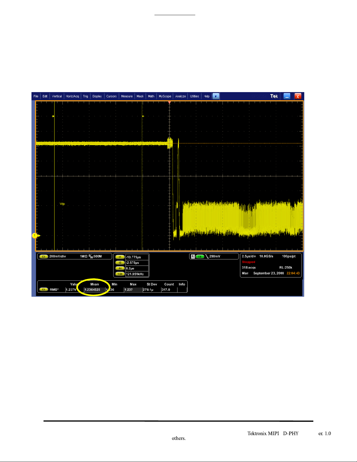
Test 1.1.1 – Data Lane LP-TX Thevenin Output High Level Voltage (VOH)
Purpose: To verify that the Thevenin Output High Level Voltage (VOH) of the DUT’s Data Lane LP transmitter is
within the conformance limits.
References:
[1] D-PHY* Standard, Section 8.1.2, Line 1382
[2] Ibid, Section 8.1.2, Table 18
[3] UNH* D-PHY* Conformance Test Suite, ver0.08, Test 1.1.1
Resource Requirements: Real-time DSO, D-PHY* test signal generator.
Last Modification: October 16, 2009
Discussion [3]:
The D-PHY Specification states, “VOH is the Thevenin output, high-level voltage in the high-level state,
when the pad pin is not loaded.” [1].
In this test, the DUT’s Data Lane VOH values will be measured using a high-speed, real-time DSO while
the DUT is driving an LP signaling sequence into an open termination. (Note that this test may be performed
while the DUT is sourcing a fixed LP-11 state, but is typically intended to be performed in conjunction with the
other tests in this group on a single captured LP Escape Mode sequence waveform, in which case the
measurement is performed on the output- high bits only.) For the measurement, VOH is measured as the
mode of all waveform samples that are greater than
50% of the absolute peak-to-peak VDP and VDN signal amplitudes. (Note that this measurement is performed
separately on both the VDP and VDN waveforms, and for each DUT Data Lane.)
The value of VOH for both the VDP and VDN signals for each Data Lane shall be between 1.1 V and 1.3
V in order to be considered conformant [2].
Test Setup: See Appendices A and B.
Test Procedure:
1. Connect the DUT to the Test System (See Appendix A).
2. Create a condition that causes the DUT to source a continuous LP-11 state.
3. Recall setup file “D-PHY_Test_1_1_1_Voh.set”. Press Single button to reach the desired part of
Page 8
® *
MOI v
8
*: Other names and brands may be claimed as the property of
Tektronix, Inc.
the signal.
4. Note the value of Mean RMS as VOH.
• Place cursors in the LP-11 part of the signal.
• Go to Measure→ Amplitude→ RMS.
• Ensure that the correct source is chosen and cursor gating is applied.
5. Repeat for Channel 2 (DN) and note the result
.
Observable Results:
• Verify that VOH for the VDP waveform is between 1.1 and 1.3 Volts for each Data Lane.
• Verify that VOH for the VDN waveform is between 1.1 and 1.3 Volts for each Data Lane.
Page 9

® *
MOI v
9
*: Other names and brands may be claimed as the property of
Tektronix, Inc.
Test 1.1.2 – Data Lane LP-TX Thevenin Output Low Level Voltage (VOL)
Purpose: To verify that the Thevenin Output Low Level Voltage (VOL) of the DUT’s Data Lane LP transmitter is
within the conformance limits.
References:
[1] D-PHY* Standard, Section 8.1.2, Line 1381
[2] Ibid, Section 8.1.2, Table 18
[3] UNH* D-PHY* Conformance Test Suite, ver0.08, Test 1.1.2
Resource Requirements: Real-time DSO, D-PHY* test signal generator.
Last Modification: October 16, 2009
Discussion [3]:
The D-PHY Specification states, “VOL is the Thevenin output, low-level voltage in the LP transmit
mode. This is the voltage at an unloaded pad pin in the low-level state.” [1].
In this test, the DUT’s Data Lane VOL values will be measured using a high-speed, real-time DSO while
the DUT is driving an LP signaling sequence into an open termination. (Note that this test is intended to be
performed in conjunction with the other tests in this group on a single captured LP Escape Mode sequence
waveform, in which case the measurement is performed on the output-low bits only.) For the purpose of this
measurement, VOL is measured as the mode of all waveform samples that are less than 50% of the absolute
peak-to-peak VDP and VDN signal amplitudes. (Note that this measurement is performed separately on both
the VDP and VDN waveforms, and for each DUT Data Lane.)
The value of VOL for both the VDP and VDN signals for each Data Lane shall be between –50 mV and +50 mV
in order to be considered conformant [2].
Test Setup: See Appendix A and B.
Test Procedure:
1. Connect the DUT to the Test System (See Appendix B).
2. Create a condition that causes the DUT to source a continuous LP-00 state.
3. Load the setup file named D-PHY_Test_1_1_2_Vol.set. (Timebase settings changed to
accommodate more edges)
4. Press single to go to the desired part of the signal
4. Make sure cursors are set to cover only the portion of the waveform where both Dp and Dn
are simultaneously low. Read the Channel1 and Channel2 RMS voltage measurement from the
display.
Page 10
® *
MOI v
10
*: Other names and brands may be claimed as the property of
Tektronix, Inc.
Observable Results:
• Verify that VOL for the VDP waveform is between -50 and +50 mV for each Data Lane.
• Verify that VOL for the VDN waveform is between -50 and +50 mV for each Data Lane.
Test 1.1.3 – Data Lane LP-TX 15%-85% Rise Time (TRLP)
Purpose: To verify that the 15%-85% Rise Time (TRLP) of the DUT’s Data Lane LP transmitter is within the
conformance limits.
References:
[1] D-PHY* Specification, Section 8.1.2, Line 1395
[2] Ibid, Section 8.1.2, Table 19
[3] UNH* D-PHY* Conformance Test Suite, ver0.08, Test 1.1.3
Resource Requirements: Real-time DSO, D-PHY* test signal generator.
Last Modification: October 16, 2009
Discussion [3]:
The D-PHY Specification states, “The times TRLP and TFLP are the 15%-85% rise and fall times,
respectively, of the output signal voltage, when the LP transmitter is driving a capacitive load CLOAD. The 15%-
Page 11

® *
MOI v
11
*: Other names and brands may be claimed as the property of
Tektronix, Inc.
85 % levels are relative to the fully settled VOH and VOL voltages.” [1].
In this test, the two single-ended VDP and VDN signals from the DUT’s Data Lane LP transmitter will be
captured using two channels of a real-time DSO. Using the measured VOH and VOL LP-TX Thevenin Output
Voltage Levels as references, the 15%-85% Rise Time (TRLP) will be measured independently for each rising
edge of the VDP and VDN waveforms. The mean value across all observed rising edges will be computed to
produce the final TRLP result, and the maximum and minimum observed values will be reported as informative
results.
The value of TRLP for VDP and VDN shall be less than 25ns in order to be considered conformant [2].
Test Setup: See Appendix A and B.
Test Procedure:
1. Connect the DUT to the Test System (See Appendix B).
2. Recall setup “D-PHY_Test_1_1_3_tRLP.set”.
3. Press single to go to the desired part of the signal.
4. Measure TRLP from the Rise time values.
Observable Results:
• Verify that TRLP is less than 25 ns for the VDP waveform for all CLOAD cases for each Data Lane.
• Verify that TRLP is less than 25 ns for the VDN waveform for all CLOAD cases for each Data Lane.
Page 12

® *
MOI v
12
*: Other names and brands may be claimed as the property of
Tektronix, Inc.
Test 1.1.4 – Data Lane LP-TX 15%-85% Fall Time (TFLP)
Purpose: To verify that the 15%-85% Fall Time (TFLP) of the DUT’s Data Lane LP transmitter is within the
conformance limits.
References:
[1] D-PHY* Specification, Section 8.1.2, Line 1395
[2] Ibid, Section 8.1.2, Table 19
[3] UNH* D-PHY* Conformance Test Suite, ver0.08, Test 1.1.4
Resource Requirements: Real-time DSO, D-PHY* test signal generator.
Last Modification: October 16, 2009
Discussion [3]:
The D-PHY Specification states, “The times TRLP and TFLP are the 15%-85% rise and fall times,
respectively, of the output signal voltage, when the LP transmitter is driving a capacitive load CLOAD. The 15%
to
85% levels are relative to the fully settled VOH and VOL voltages.” [1].
In this test, the two single-ended VDP and VDN signals from the DUT’s Data Lane LP transmitter will be
captured using two channels of a real-time DSO. Using the measured VOH and VOL LP-TX Thevenin Output
Voltage Levels as references, the 15% to 85% Fall Time (TFLP) will be measured independently for each falling
edge of the VDP and VDN waveforms. The mean value across all observed falling edges will be computed to
produce the final TFLP result, and the maximum and minimum observed values is reported as informative
results.
The value of TFLP for VDP and VDN shall be less than 25 ns in order to be considered conformant [2].
Test Setup: See Appendix A and B.
Test Procedure:
1. Connect the DUT to the Test System (See Appendix B).
2. Recall setup “D-PHY_Test_1_1_4_tFLP.set”.
3. Press single to go to the desired part of the signal.
4. Measure TFLP from the Fall time values.
Page 13
® *
MOI v
13
*: Other names and brands may be claimed as the property of
Tektronix, Inc.
Observable Results:
• Verify that TFLP is less than 25 ns for the VDP waveform for all CLOAD cases for each Data Lane.
• Verify that TFLP is less than 25 ns for the VDN waveform for all CLOAD cases for each Data Lane.
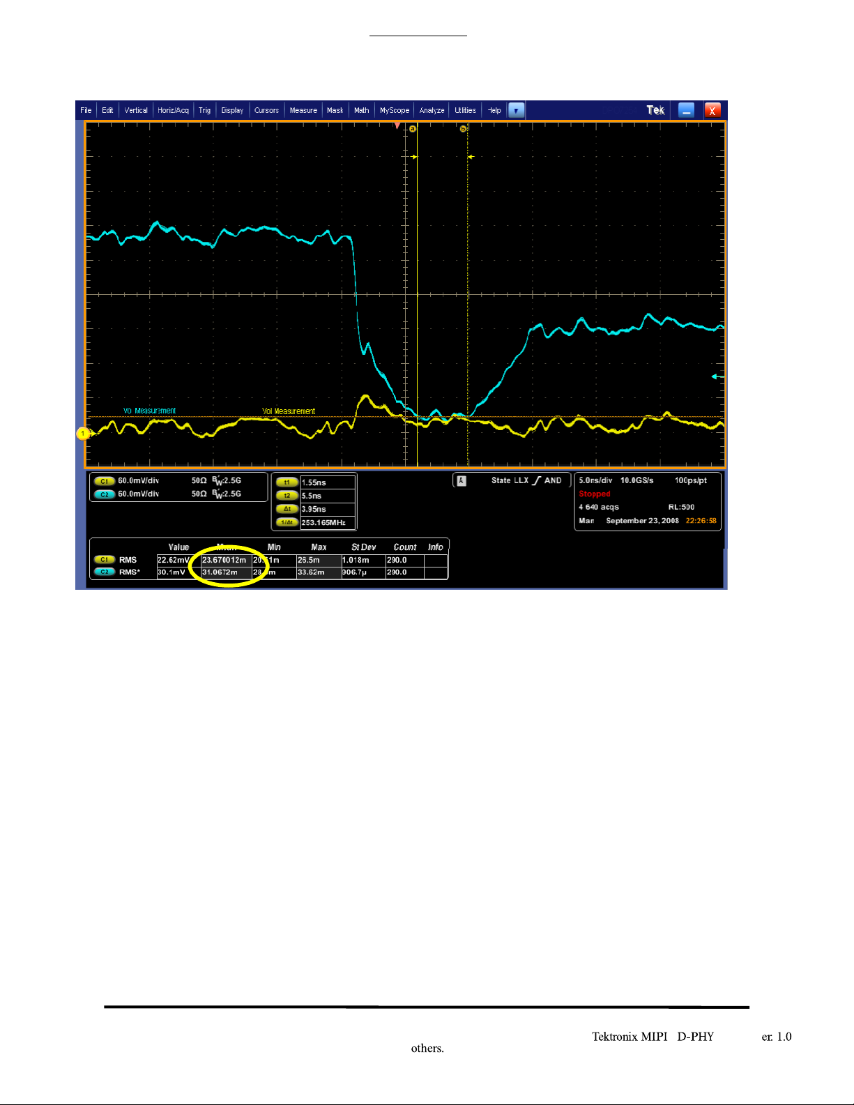
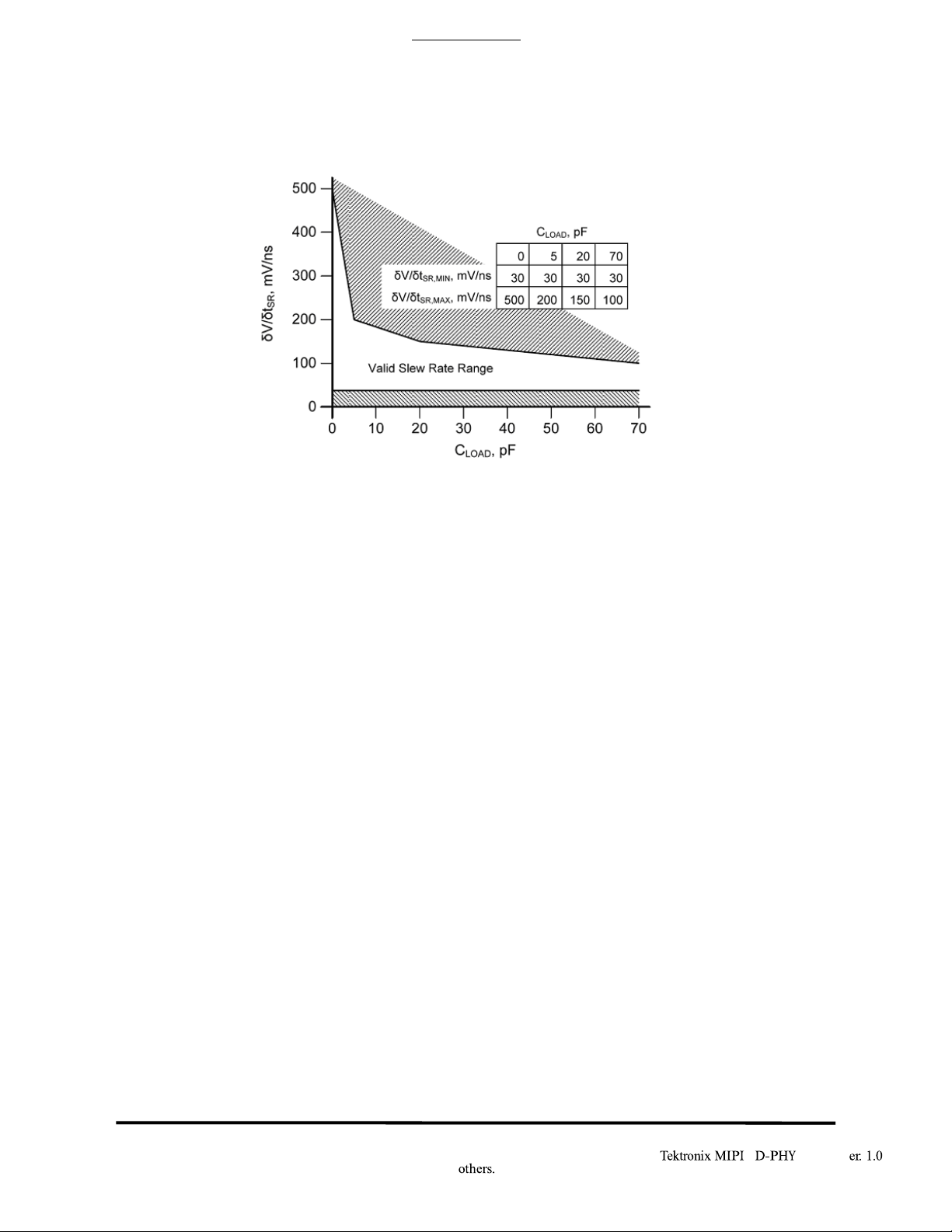
Test 1.1.5 – Data Lane LP-TX Slew Rate vs. CLOAD (δV/δtSR)
Purpose: To verify that the Slew Rate (δV/δtSR) of the DUT’s Data Lane LP transmitter is within the
conformance limit, for different capacitive loading conditions.
References:
[1] D-PHY* Specification, Section 8.1.2, Line 1397
[2] Ibid, Section 8.1.2, Table 19 [3] Ibid, Section 8.1.2, Figure 45
[4] UNH* D-PHY* Conformance Test Suite, ver0.08, Test 1.1.5
Resource Requirements: Real-time DSO, D-PHY* test signal generator.
Last Modification: October 16, 2009
Discussion [4]:
The D-PHY Specification states, “The slew rate δV/δtSR is the derivative of the LP transmitter output
signal voltage over time. The slew rate specification shall be met for the 15% - 85% range while driving a
Page 14
® *
MOI v
14
*: Other names and brands may be claimed as the property of
Tektronix, Inc.
capacitive load, CLOAD.” [1]. A Figure is provided in the specification that shows a graphical representation of
the Slew Rate conformance range, is reproduced below.
Figure: Slew Rate vs. CLOAD Mask
The specific values are defined in [2] as:
• δV/δtSR into CLOAD = 0pF shall be between 30 and 500 mV/ns.
• δV/δtSR into CLOAD = 5pF shall be between 30 and 200 mV/ns.
• δV/δtSR into CLOAD = 20pF shall be between 30 and 150 mV/ns.
• δV/δtSR into CLOAD = 70pF shall be between 30 and 100 mV/ns.
The specification also states that the maximum Slew Rate requirement is to be measured when the
output voltage is between 15% and below 85% of the “fully settled LP signal levels” and is measured as an
average across any 50 mV segment of the output signal transition.
Also note that the minimum Slew Rate requirement is applicable over the vertical region between 400
and
930 mV across any 50 mV segment of the output signal transition. [2]. (This is different from the applicable
range for the maximum Slew Rate specification.)
Page 15

® *
MOI v
15
*: Other names and brands may be claimed as the property of
Tektronix, Inc.
In this test, the two single-ended VDP and VDN signals from the DUT’s Data Lane LP transmitter is
captured using two channels of a real-time DSO. The Slew Rate is measured independently for each edge of the
VDP and VDN signals. Maximum and minimum Slew Rate values is computed and reported for each rising and
falling edge, across the applicable vertical ranges using a 50 mV vertical window. The measurement is repeated
for all CLOAD cases, and for all Data Lanes.
Test Setup: See Appendix A and B.
Test Procedure:
1. Connect the DUT to the Test System (See Appendix B).
2. Configure the load termination for CLOAD = 0pF.
3. Create a condition that causes the DUT to source an LP Escape Mode sequence on Data Lane 0.
4. From the oscilloscope main menu, select Analyze > Jitter and Eye Analysis > Select.
5. Recall setup file D-PHY_Test_1_1_5_SlewrFLP.set.
6. Press Single button on the oscilloscope panel to reach the desired part of the signal.
7. Apply cursors to the specific part of the signal with rising and falling edges.
8. Press Single on DPOJET to make the measurement.
Repeat the previous steps for CLOAD values of 5 pF, 20 pF, and 70 pF.
10. Repeat the previous steps for Data Lanes 1, 2, and 3 (if the DUT implements multiple Data
Lanes).
9.
Page 16

® *
MOI v
16
*: Other names and brands may be claimed as the property of
Tektronix, Inc.
Observable Results:
• Verify that the maximum δV/δtSR into a CLOAD of 0 pF is less than 500 mV/ns, for each Data Lane.
• Verify that the maximum δV/δtSR into a CLOAD of 5 pF is less than 200 mV/ns, for each Data Lane.
• Verify that the maximum δV/δtSR into a CLOAD of 20 pF is less than 150 mV/ns, for each Data Lane.
• Verify that the maximum δV/δtSR into a CLOAD of 70 pF is less than 100 mV/ns, for each Data Lane.
• For all load cases, verify that the minimum δV/δtSR is greater than 30 mV/ns, for each Data Lane.
Page 17

® *
MOI v
17
*: Other names and brands may be claimed as the property of
Test Name
Setup File
Test 1.2.1 – Clock Lane LP-TX Thevenin Output High Level Voltage(VOH)
D-PHY_Test_1_2_1_Voh.set
Test 1.2.2 – Clock Lane LP-TX Thevenin Output Low Level Voltage (VOL)
D-PHY_Test_1_2_2_Vol.set.
Test 1.2.3 – Clock Lane LP-TX 15%-85% Rise Time (TRLP)
D-PHY_Test_1_2_3_tRLP.set”.
Test 1.2.4 – Clock Lane LP-TX 15%-85% Fall Time (TFLP)
D-PHY_Test_1_2_4_tFLP.set”.
Test 1.2.5 – Clock Lane LP-TX Slew Rate vs. CLOAD (δV/δtSR)
D-PHY_Test_1_2_5_SlewrFLP.set
Tektronix, Inc.
GROUP 2: CLOCK LANE LP TX ELECTRICALS
All the Measurements in this group are similar to the measurements in Group 1, except that this uses the clock
lanes instead of the data lanes. So connect the Differential clock lane (Vcp, Vcn) to the scope channels (Ch3 ,
Ch4) respectively.
The Table below gives the setups used for these group2 measurements
Page 18

® *
MOI v
18
*: Other names and brands may be claimed as the property of
Tektronix, Inc.
GROUP 3: HS TX ELECTRICAL TESTS
Overview:
This group of tests verifies the High Speed TX electrical requirements of the data lane as defined in the
D-PHY* Standard.
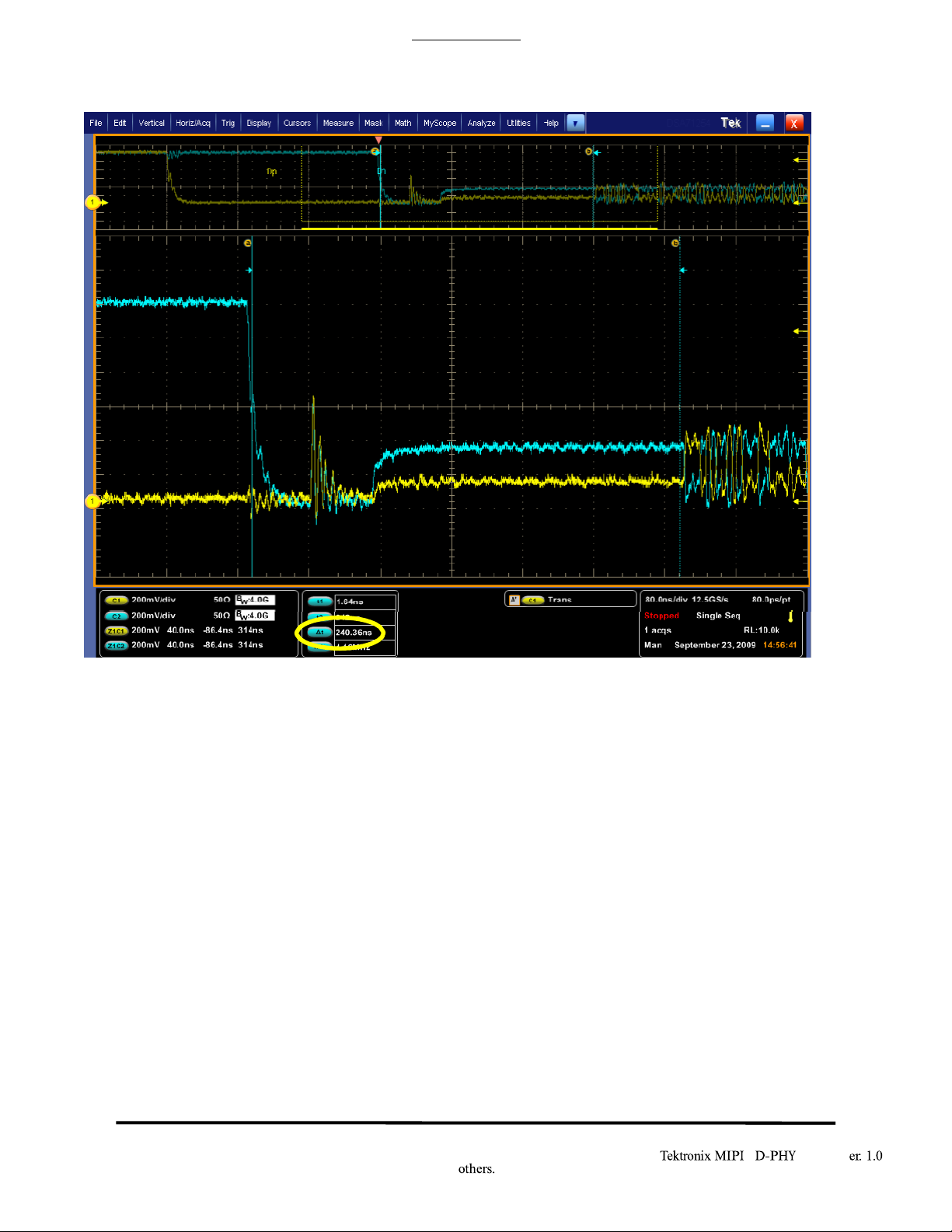
TEST 1.3.1 – DATA LANE HS ENTRY: DATA LANE TLPX VALUE
Purpose: To verify that the HS AC Common-Mode Signal Level Variations above 450 MHz (VCMTX(HF)) of the
DUT transmitter are below the maximum allowable limit.
References:
[1] D-PHY* Specification, Section 5.2, Line 746
[2] Ibid, Section 5.9, Table 14
[3] UNH* D-PHY* Conformance Test Suite, ver0.08, Test 1.3.1
Resource Requirements: Real-time DSO, D-PHY* test signal generator.
Last Modification: October 16, 2009
Discussion[3]:
The D-PHY Low-Power (LP) mode of operation is comprised of state transitions occurring at some
implementation-
specific rate less than 20M transitions/sec. Note that these state transitions may have different meanings
depending on the context (Control, Escape, or LPDT mode), and do not equate to ‘bits’ on the wire. The D-PHY
Specification specifies that, “All LP state periods shall be at least TLPX in duration.” [1], and defines the
minimum value of TLPX to be 50 ns [2].
In this test, the focus is specifically the duration of the last LP-01 state that occurs immediately before
an HS burst sequence. The state will be measured starting at the time where the VDP falling edge crosses
below the maximum low-level LP threshold, VIL,MAX (550 mV), and ending at the time where the VDN falling
edge crosses below the same VIL,MAX threshold. A picture of the TLPX interval is shown in the figure below.
Test Setup: See Appendix A and B.
Test Procedure:
1. Recall setting file “D-PHY_Test_1_3_1_tLPX.set” using the main menu: File/Recall…/Setup
2. Press the Multiview Zoom button and then press Single on the oscilloscope.
3. Verify if the zoom is correctly located as per the diagram shown above.
4. Note the minimum value of Delay between Ch1 and Ch2 at the bottom of the screen.
Page 19

® *
MOI v
19
*: Other names and brands may be claimed as the property of
Tektronix, Inc.
5. The value should be greater than 50 ns to meet the required specification.
Page 20

® *
MOI v
20
*: Other names and brands may be claimed as the property of
Observable Results:
• Verify that TLPX value is greater than 50 ns.
Tektronix, Inc.
Test 1.3.2 – Data Lane HS Entry: THS-PREPARE Value
Purpose: To verify that the duration of the final LP-00 state immediately before HS transmission (THS-
PREPARE) is within the conformance limits.
References:
[1] D-PHY* Specification, Section 5.14.2, Line 1027
[2] Ibid, Section 5.9, Table 14
[3] UNH* D-PHY* Conformance Test Suite, ver0.08, Test 1.3.2
Resource Requirements: Real-time DSO, D-PHY* test signal generator.
Last Modification: October 16, 2009
Discussion [3]:
As part of the process for switching the Data Lane into HS mode, the D-PHY Specification provides a
specification for the minimum time interval that a device must transmit the final LP-00 state before enabling
HS mode (which occurs at the start of the THS-ZERO interval). This interval is defined as THS-PREPARE, and is
shown in the figure below.
Page 21

® *
MOI v
21
*: Other names and brands may be claimed as the property of
Tektronix, Inc.
Figure: THS-PREPARE Interval
In this test, the DUT will be configured to source an HS burst sequence, starting and ending with LP-11
states. The THS-PREPARE interval begins at the time where the Data Lane VDN signal crosses below VIL,MAX
(550 mV), and ends at the beginning of the extended THS-ZERO HS differential state, at the point where the
VOD differential voltage crosses above the minimum valid HS-RX differential threshold level (+/-70 mV). The
measured duration of THS-PREPARE should be between (40 ns + 4*UI) and (85 ns + 6*UI) (where UI is the
nominal HS Unit Interval for the DUT) in order to be considered conformant.
Test Setup: See Appendix A and B.
Test Procedure:
1. Recall setting file “D-PHY_Test_1_3_2_tHSprep.set”, using the main menu: File/Recall…/Setup
2. Ensure the cursors are marked at the location as per the diagram above.
3. Note the value of ∆t as THS-PREPARE
4. Calculate the limits (40 ns + 4*UI) and (85 ns + 6*UI). Confirm that as THS-PREPARE is between
these limits.
Page 22

® *
MOI v
22
*: Other names and brands may be claimed as the property of
Tektronix, Inc.
Observable Results:
• Verify that THS-PREPARE is within the limits of (40 ns + 4*UI) and (85 ns + 6*UI).
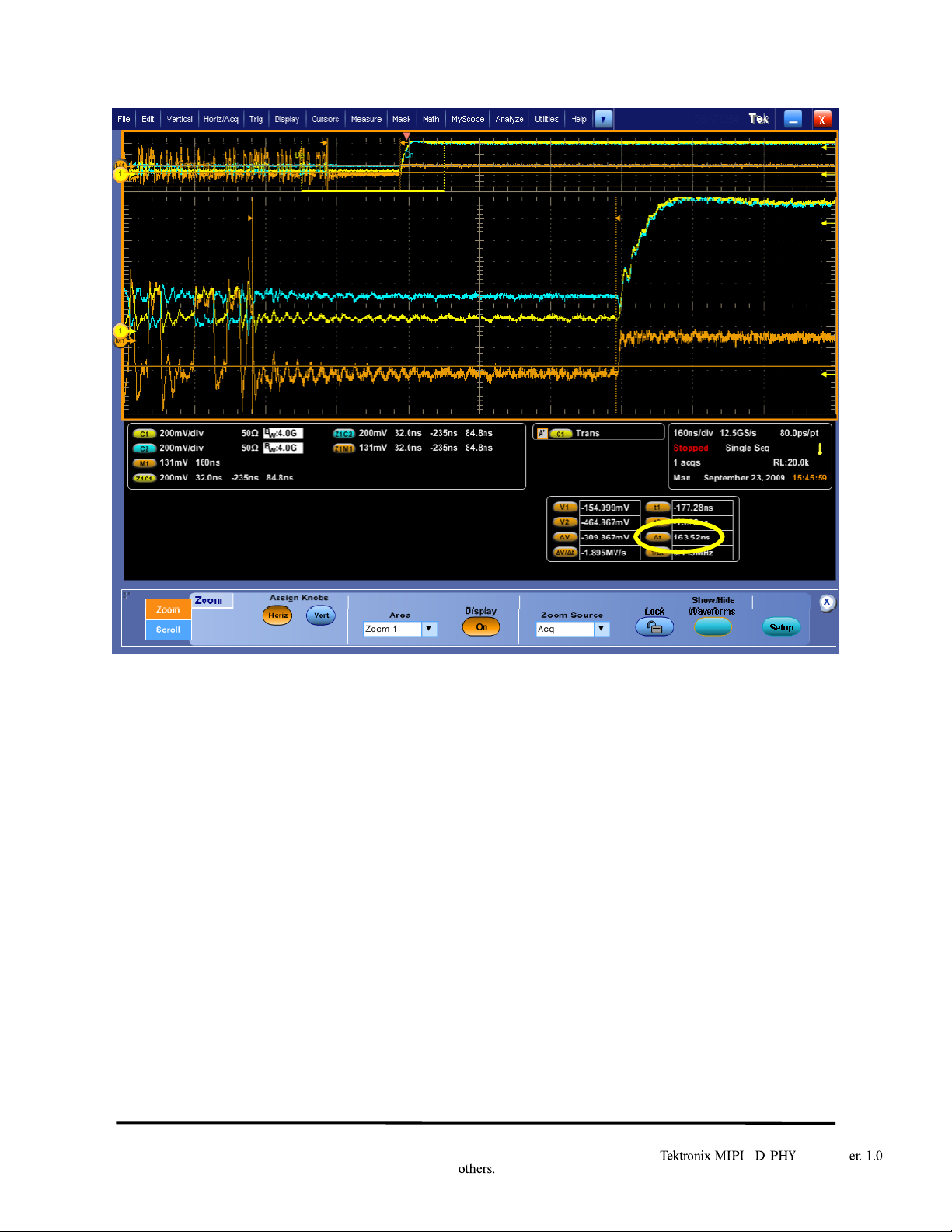
Test 1.3.3 – Data Lane HS Entry: THS-PREPARE + THS-ZERO Value
Purpose: To verify that the combined time of THS-PREPARE plus the time the DUT Data Lane transmitter drives
the HS-0 differential state prior to transmitting the HS Sync sequence (THS-ZERO) is greater than the
minimum required duration.
References:
[1] D-PHY* Standard, Section 5.14.2, Line 1028
[2] Ibid, Section 5.9, Table 14
[3] UNH* D-PHY* Conformance Test Suite, ver0.08, Test 1.3.3
Resource Requirements: Real-time DSO, D-PHY* test signal generator.
Last Modification: October 16, 2009
Discussion [3]:
As part of the process for switching the Data Lane into HS mode, the D-PHY Specification provides a
specification for the minimum duration that a device must drive the extended Data HS-0 differential state
Page 23

® *
MOI v
23
*: Other names and brands may be claimed as the property of
Tektronix, Inc.
prior to starting HS differential data transmission. This interval is defined as THS-ZERO, and is shown in the
figure below.
Figure: THS-ZERO Interval
In this test, the DUT will be configured to source an HS burst sequence, starting and ending with LP-11
states. The (THS-PREPARE + THS-ZERO) interval begins at the time where the Data Lane VDN signal crosses
below VIL,MAX (550 mV), and ends at the end of the extended THS-ZERO HS-0 differential state, at the point
corresponding to the start of the first bit of the HS Sync sequence. (Note this point is not at the first HS-1
transition, but rather three HS Unit Intervals prior, as the Sync sequence starts with 0001. Thus there is no
visible delineation between the extended HS-0 and the first HS-0 of the Sync sequence.) The measured
duration of (THS-PREPARE + THS-ZERO) should be greater than (145 ns + 10*UI) ns (where UI is the nominal HS
Unit Interval for the DUT) in order to be considered conformant.
Test Setup: See Appendix A and B.
Test Procedure:
1. Connect the DUT to the Test System (See Appendix A)
2. Recall setup file “D-PHY_Test_1_3_3_tHSp_tHs0.set”. Press Single button to capture the
desired part of the signal.
3. (Note: If you do not see the zoomed portion of the signal, press the Multiview Zoom button.)
4. Ensure that the cursors are placed as per the diagram above. Include both THS-PREPARE + THS-
ZERO
when taking measurement. Note the ∆t value as the total THS-PREPARE + THS-ZERO.
5. Repeat for each data lane.
Page 24
® *
MOI v
24
*: Other names and brands may be claimed as the property of
Tektronix, Inc.
Observable Results:
• Verify that (THS-PREPARE + THS-ZERO) is greater than (145ns + 10*UI) ns for each Data Lane.
Page 25

® *
MOI v
25
*: Other names and brands may be claimed as the property of
Tektronix, Inc.
Test 1.3.4 – Data Lane HS TX Differential Voltage (VOD)
Purpose: To verify that the Differential Voltages (VOD(0) and VOD(1)) of the DUT Data Lane HS transmitter are
within the conformance limits.
References:
[1] D-PHY* Specification, Section 8.1.1, Line 1318
[2] Ibid, Section 8.1.1, Figure 38 [3] Ibid, Section 8.1.1, Table 16
[4] UNH* D-PHY* Conformance Test Suite, ver0.08, Test 1.3.4
Resource Requirements: Real-time DSO, D-PHY* test signal generator.
Last Modification: October 16, 2009
Discussion[4]:
The D-PHY Specification states, “The differential output voltage VOD is defined as the difference of the
voltages VDP and VDN at the Dp and Dn pins, respectively. VOD = VDP – VDN.” [1]. Note that this definition
is potentially ambiguous in that, while it does define how the differential signal is computed, it does not
specify how the differential voltage is measured for the purposes of conformance testing. (Note that a
diagram is presented in [2], but this shows ‘ideal’ signaling, which is not an accurate representation for
measurement purposes.) Given that there are multiple possible ways to implement a differential voltage
measurement (peak-to-peak, mode-to-mode,
average over entire UI, average over 40%-60% UI, etc), a common method must be chosen for consistency. A
simple averaged method is defined here, using the averaged HS-1 and HS-0 voltage levels at the center of each
Unit Interval.
In this test, a sample of the DUT’s HS Data Lane signaling will be captured using a real-time DSO. The
differential waveform VOD will be computed as difference of the positive and negative single-ended
waveforms (VDP-VDN). The differential waveform VOD will then be sampled at the center of each Unit
Interval in order to determine the VOD(0) and VOD(1) values, which will each be averaged over all of the bits
in an entire HS burst to produce the averaged VOD(0) and VOD(1) values. The averaged VOD(1) value must be
within the range of 140 to 270 mV in order to be considered conformant [3]. The averaged VOD(0) value must
be within the range of -140 to -270 mV in order to be considered conformant [3]. (Note that this equates to a
differential peak-to-peak voltage value of 280 to 540 mVppd.)
(Must add test cases to cover ZID requirements.)
Test Setup: See Appendix A and B.
Test Procedure:
1. Connect the DUT to the Test System (See Appendix B)
2. Configure the Test System to emulate the DUT link partner (Master or Slave).
3. Launch DPOJET using the main menu: Analyze/Jitter and Eye Analysis.
4. Recall setting file “D-PHY_Test_1_3_4_Vod.set.” using the main menu: File/Recall…/Setup.
5. Put the cursors in high speed region
Page 26

® *
MOI v
26
*: Other names and brands may be claimed as the property of
Tektronix, Inc.
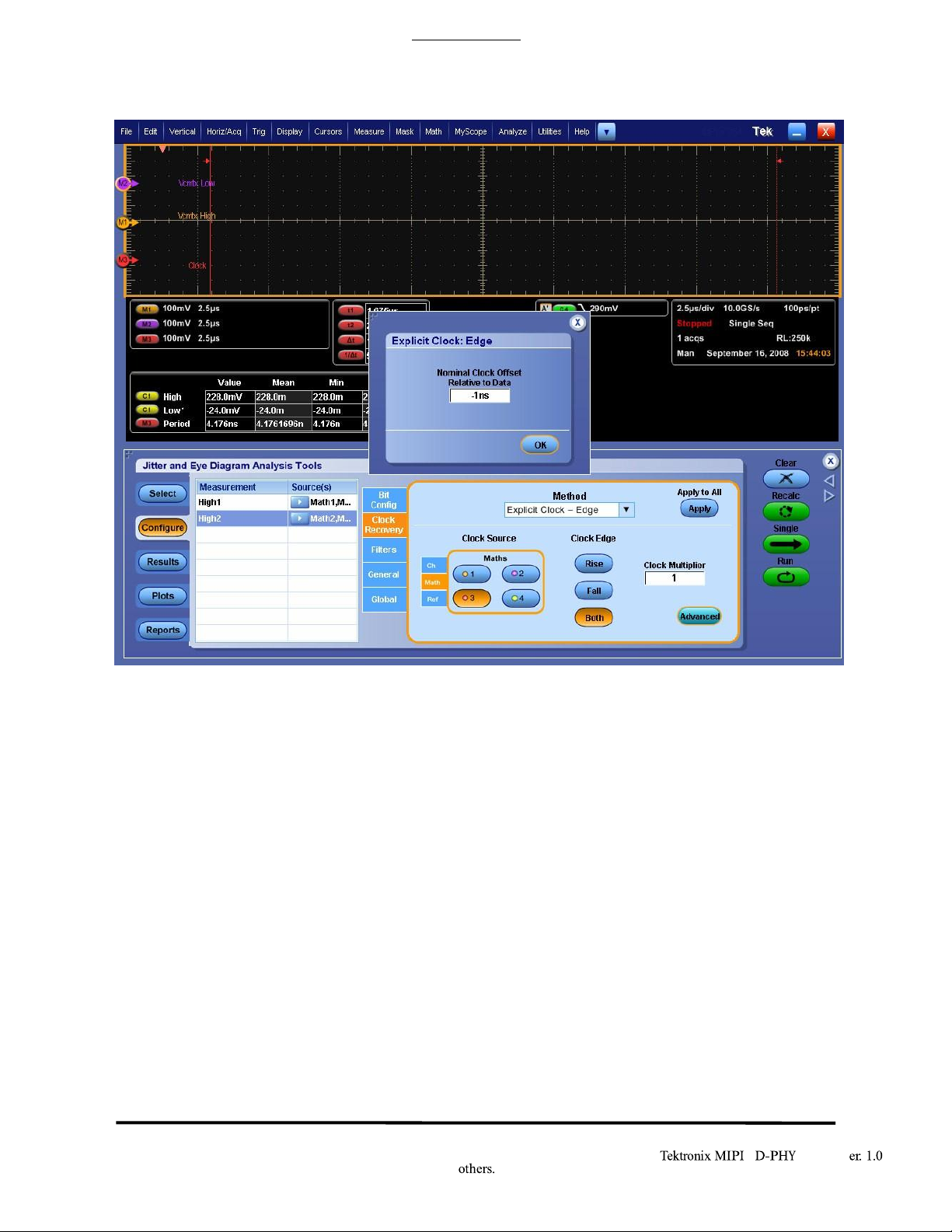
3. Click on the “Configure” button in DPOJET. Click on “Clock Recovery”. Click on “Advanced”. Enter in a value
that is approx. ¼ of value shown in M3 Mean display (enter a negative value).
Page 27

® *
MOI v
27
*: Other names and brands may be claimed as the property of
Tektronix, Inc.
5. Click on “Results”, and click on “Run”. This will make multiple acquisitions until 10,000 have
been acquired.
6. Read the measured values for High1 (VOD High) and High2 (VOD Low) from the results table
(mean value).
7. Compare against test limits of 140 mV and 270 mV.
Page 28

® *
MOI v
28
*: Other names and brands may be claimed as the property of
Tektronix, Inc.
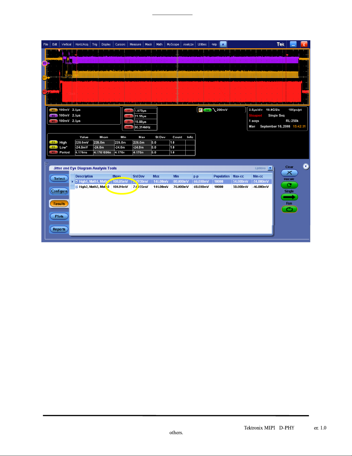
Observable Results:
• Verify that VOD High is between 140 and 270 mV (i.e. 280 to 540 mVppd)
• Verify that VOD Low is between -140 and -270 mV (i.e. -280 to -540 mVppd)
Note: The Gated Cursor must be adjusted if required and should be placed in between the payload region
as shown in above Figure.
Page 29

® *
MOI v
29
*: Other names and brands may be claimed as the property of
Tektronix, Inc.
Test 1.3.5 – Data Lane HS TX Differential Voltage Mismatch (∆VOD)
Purpose: To verify that the Differential Voltage Mismatch (∆VOD) of the DUT Data Lane HS transmitter is
within the conformance limits.
References:
[1] D-PHY* Specification, Section 8.1.1, Line 1330
[2] Ibid, Section 8.1.1, Table 16
[3] UNH* D-PHY* Conformance Test Suite, ver0.08, Tes t1.3.5
Resource Requirements: Real-time DSO, D-PHY* test signal generator.
Last Modification: October 16, 2009
Discussion[3]:
The D-PHY Specification states, “The output differential voltage mismatch ∆VOD is defined as the
difference of the absolute values of the differential output voltage in the Differential-1 state VOD(1) and
the differential output voltage in the Differential-0 state VOD(0). This is expressed by ∆VOD = | VOD(1)| - |
VOD(0)|” [1].
In this test, the numerical VOD(0) and VOD(1) results obtained in the previous test (see Test 1.3.4) will
be used to compute the ∆VOD result. The difference of the absolute values of these two values will be taken
to produce ∆VOD. The absolute value of ∆VOD must be less than 10 mV in order to be considered conformant
[2].
(Must add test cases to cover ZID requirements.)
Test Setup: See Appendix A.
Test Procedure:
1. Perform test 1.3.4 as previously described.
2. Launch DPOJET using the main menu: Analyze/Jitter and Eye Analysis.
3. Recall setting file “D-PHY_Test_1_3_4_Vod.set” using the main menu: File/Recall…/Setup
4. Obtain VOD0 and VOD1 as in test 1.3.4, and compute the absolute difference, which shall be
less than 10mV to be conformant
Page 30

® *
MOI v
30
*: Other names and brands may be claimed as the property of
Tektronix, Inc.
4.
Read mean values for High1 and High2 as highlighted above.
5. Compute the mismatch by: ∆VOD = abs(High1)-abs(High2).
6. Compare mismatch against observable results.
Observable Results:
• Verify that the absolute value of ∆VOD is less than 10 mV.
Test 1.3.6 – Data Lane HS TX Single-Ended Output High Voltage (VOHHS)
Purpose: To verify that the Single-Ended Output High Voltages (VOHHS (DP) and VOHHS (DN)) of the DUT Data
Lane. HS transmitter is less than the maximum conformance limit.
References:
[1] D-PHY* Specification, Section 8.1.1, Line 1321
[2] Ibid, Section 8.1.1, Table 16
[3] UNH* D-PHY* Conformance Test Suite, ver0.08, Test 1.3.6
Resource Requirements: Real-time DSO, D-PHY* test signal generator.
Last Modification: October 16, 2009
Discussion [3]:
Page 31

® *
MOI v
31
*: Other names and brands may be claimed as the property of
Tektronix, Inc.
The D-PHY Specification states, “The output voltages VDP and VDN at the Dp and Dn pins shall not
exceed the High-Speed output high voltage VOHHS. VOLHS is the High-Speed output, low voltage on Dp and
Dn and is determined by VOD and VCMTX. The High-Speed VOUT is bounded by the minimum value of VOLHS
and the maximum value of VOHHS.” [1].
In this test, a sample of the DUT’s HS Data Lane signaling will be captured using a real-time DSO. The
VDP and VDN single-ended waveforms will be captured using separate channels of the DSO, and processed
independently. The maximum instantaneous voltages for both the VDP and VDN signals measured across the
entire HS burst (between the end of THS-ZERO and the start of THS-TRAIL) will be recorded as VOHHS. (Note
these will be denoted as VOHHS (DP) and VOHHS (DN) for the purpose of this test, though they are not
explicitly defined this way in the specification.) The VOHHS results for both VDP and VDN shall be less than
360 mV in order to be considered conformant [2].
Note: - TX Vdiff range is 140-270 mV (280 to 540 mVppd)
- TX Vcm range is 150-250 mV
- TX max SE voltage (VOHHS) is 360 mV
If you run at maximum allowed TX common-mode level and maximum differential output, your single-ended
upper voltage will be 250+135 = 385 mV. Therefore, if you want to run at the maximum allowed TX singleended rail of
360 mV, you need to decrease either common-mode or diff output. (Must add test cases to cover ZID
requirements.)
Test Setup: See Appendix A and B.
Test Procedure:
1. Launch DPOJET using the main menu: Analyze/Jitter and Eye Analysis.
2. Recall setting file “D-PHY_Test_1_3_6_Voohs.set” using the main menu: File/Recall…/Setup
Page 32

® *
MOI v
32
*: Other names and brands may be claimed as the property of
Tektronix, Inc.
3. Click on the “Configure” button in DPOJET. Click on “Clock Recovery”. Click on “Advanced”. Enter a value
that is approx. ¼ of value shown in M3 Mean display (enter negative value).
Page 33
® *
MOI v
33
*: Other names and brands may be claimed as the property of
Tektronix, Inc.
3. Click on “Results”, and click on “Run”. This will make multiple acquisitions until 10,000 have
been acquired.
4. Read the measured values for High1 (VOHHS(DP)) and High2 (VOHHS(DN)) from the results
table
(Max value).
5. Compare against test limits of 360 mV.
Page 34

® *
MOI v
34
*: Other names and brands may be claimed as the property of
Tektronix, Inc.
Observable Results:
• Verify that VOHHS is less than 360 mV for both the Dp and Dn signals.
Note: The Gated Cursor must be adjusted if required and should be placed in between the payload region
as shown in above Figure.
Page 35
® *
MOI v
35
*: Other names and brands may be claimed as the property of
Tektronix, Inc.
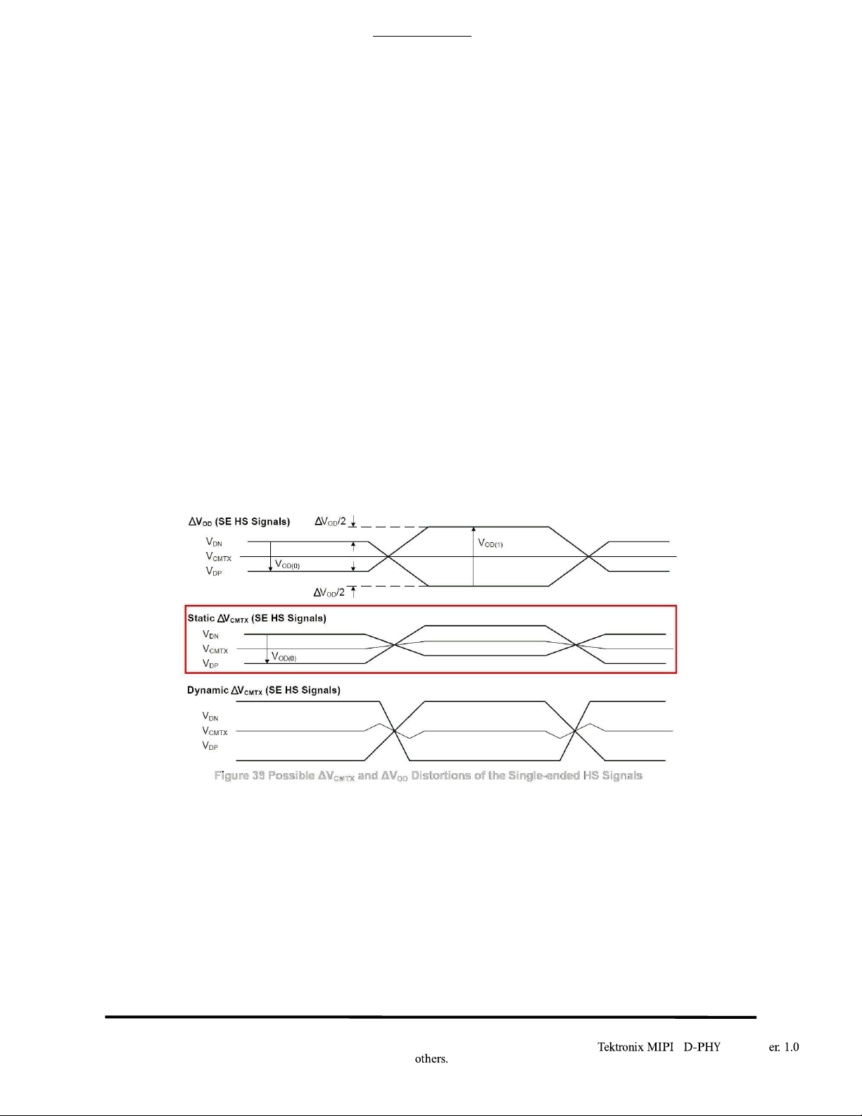
Test 1.3.7 – Data Lane HS TX Static Common-Mode Voltage (VCMTX)
Purpose: To verify that the Static Common-Mode Voltages (VCMTX High, and VCMTX Low) of the DUT Data
Lane. HS transmitter is within the conformance limits.
References:
[1] D-PHY* Specification, Section 8.1.1, Line 1325
[2] Ibid, Section 8.1.1, Figure 39 [3] Ibid, Section 8.1.1, Table 16
[4] UNH* D-PHY* Conformance Test Suite, ver0.08, Test 1.3.7
Resource Requirements: Real-time DSO, D-PHY* test signal generator.
Last Modification: October 16, 2009
Discussion [4]:
The common-mode voltage VCMTX is defined as, “the arithmetic mean value of the voltages at the Dp and Dn
pins: VCMTX = (VDP+VDN)/2” [1]. Because of various types of signal distortions that may occur, it is possible
for VCMTX to have different values when a Differential-1 vs. Differential-0 state is being driven. Because of
this, VCMTX must be measured separately for both the 0 and 1 states, at the “static” value corresponding to
the settled voltage at the center of the UI (as opposed to the “dynamic” AC fluctuations that occur at the bit
transitions, which are covered by a separate specification). The specification includes a figure showing various
different types of signal distortions that can occur [2]. This figure is reproduced below, with the static
common-mode distortion type highlighted in red.
Figure: Static VCMTX Distortion
In this test, a portion of the DUT’s HS Data Lane signaling will be captured using a real-time DSO. The VDP and
VDN single-ended waveforms will be averaged together (as described above) to create the VCMTX commonmode waveform. The VCMTX waveform will be sampled at the center of each UI, corresponding to each
Differential-1 and Differential-0 state in the HS burst. The average common-mode voltage across all
Differential-1 UIs will be computed as VCMTX(1), and the average common-mode voltage across all
Differential-0 UIs will be computed as VCMTX(0). The values for both VCMTX(1) and VCMTX(0) must be
between 150 to 250 mV in order to be considered conformant [3].
(Must add test cases to cover ZID requirements.)
Page 36
® *
MOI v
36
*: Other names and brands may be claimed as the property of
Tektronix, Inc.
Test Setup: See Appendix A and B.
Test Procedure:
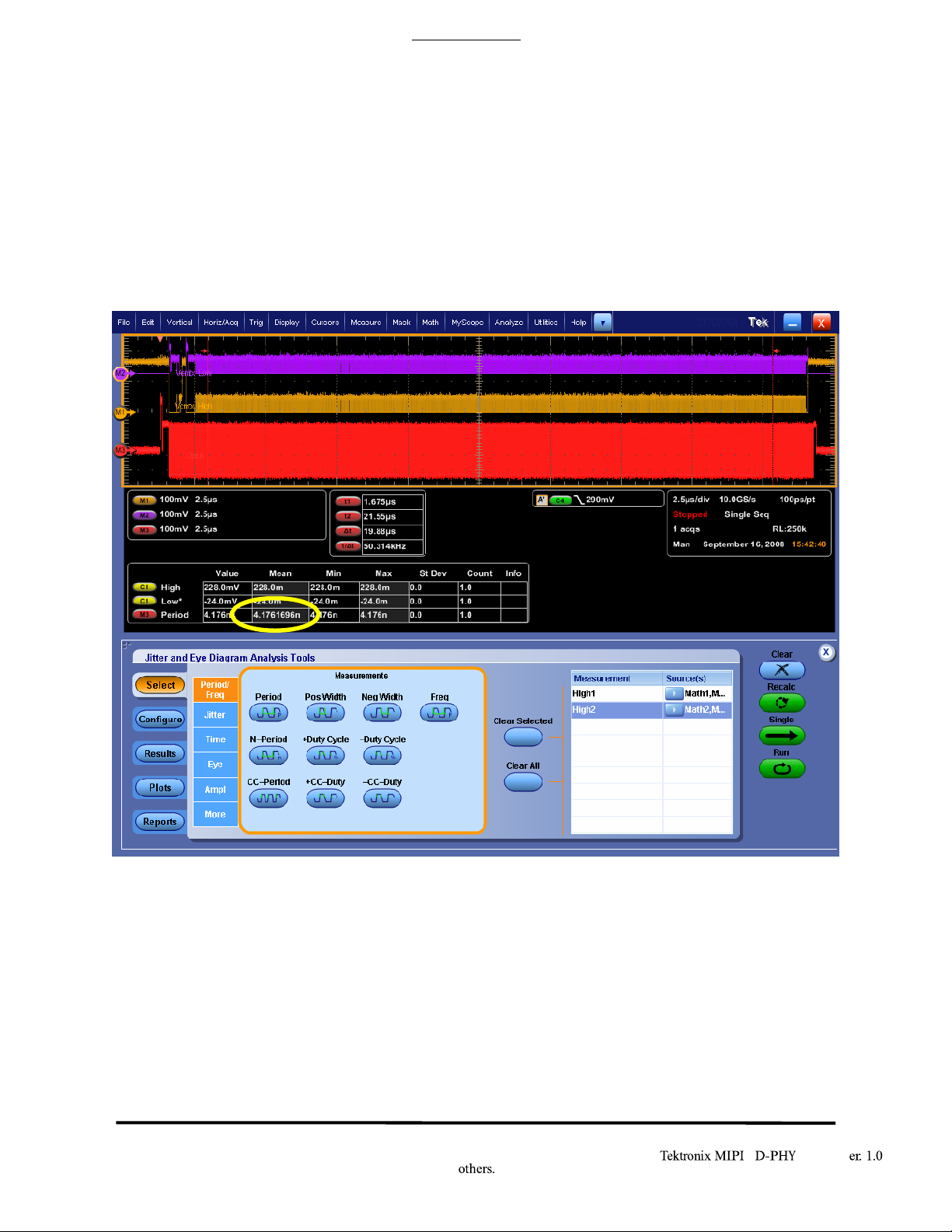
1. Connect the DUT to the Test System (See Appendix B)
2. Using DUT vendor-specific techniques, put the DUT into a state where it is transmitting a HS
data burst.
3. Launch DPOJET using the main menu: Analyze/Jitter and Eye Analysis.
3. Click the “Configure” button in DPOJET. Click on “Clock Recovery”. Click “Advanced”. Enter a value that is
approx. ¼ of value shown in M3 Mean display (enter a negative value).
4. Recall setting file “D-PHY_Test_1_3_7_Vcmtx.set”, using the main menu: File/Recall…/Setup
Page 37

® *
MOI v
37
*: Other names and brands may be claimed as the property of
Tektronix, Inc.
5. Click on “Results”, and click on “Run”. This will make multiple acquisitions until 10,000 samples
have been acquired.
6. Read the measured values for High1 (Vcmtx High) and High2 (Vcmtx Low) from the results table
(mean value).
7. Compare against test limits of 150 mV and 250 mV.
Page 38
® *
MOI v
38
*: Other names and brands may be claimed as the property of
Tektronix, Inc.
Observable Results:
• Verify that VCMTX is between 150 and 250 mV for both the Differential-1 and Differential-0 states.
Note: The Gated Cursor must be adjusted if required and should be placed in between the payload region
as shown in above Figure.
Page 39

® *
MOI v
39
*: Other names and brands may be claimed as the property of
Tektronix, Inc.
Test 1.3.8 – Data Lane HS TX VCMTX Mismatch (∆VCMTX(1,0))
Purpose: To verify that the Static Common-Mode Voltage Mismatch (∆VCMTX(1,0)) of the DUT Data Lane HS
transmitter is less than the maximum conformance limit.
References:
[1] D-PHY* Specification, Section 8.1.1, Line 1340
[2] Ibid, Section 8.1.1, Table 16
[3] UNH* D-PHY* Conformance Test Suite, ver0.08, Test 1.3.8
Resource Requirements: Real-time DSO, D-PHY* test signal generator.
Last Modification: October 16, 2009
Discussion[4]:
The specification states, “The static common-mode voltage mismatch between the Differential-1
and
Differential-0 state is given by: ∆VCMTX(1,0) = (VCMTX(1)–VCMTX(0))/2”[1].
In this test, the numerical results from Test 1.3.7 for VCMTX(1) and VCMTX(0) will be used to compute
the Data Lane HS-TX Static Common-Mode Voltage Mismatch, ∆VCMTX(1,0). The result for ∆VCMTX(1,0) will
be taken as one- half of the difference of VCMTX(1) minus VCMTX(0). The value for ∆VCMTX(1,0) must be
less than 5 mV in order to be considered conformant [2].
Test Setup: See Appendix A and B.
Test Procedure:
1. Perform setup test 1.3.7 as previously described.
Page 40
® *
MOI v
40
*: Other names and brands may be claimed as the property of
2. Read mean values for High1 and High2, as highlighted above.
3. Compute the mismatch by: ∆VCMTX(1,0) = abs(High1-High2)/2.
4. Compare mismatch against observable results.
Observable Results:
• Verify that ∆VCMTX(1,0) is less than 5 mV.
Tektronix, Inc.
Page 41

® *
MOI v
41
*: Other names and brands may be claimed as the property of
Tektronix, Inc.
Test 1.3.9 – Data Lane HS TX Common-Level Variations Between 50-450 MHz (VCMTX(LF))
Purpose: To verify that the AC Common-Mode Signal Level Variations between 50 and 450 MHz (VCMTX(LF)) of
the DUT Data Lane HS transmitter are below the maximum allowable limit.
References:
[1] D-PHY* Specification, Section 8.1.1, Line 1342
[2] Ibid, Section 8.1.1, Figure 39 [3] Ibid, Section 8.1.1, Table 17
[4] UNH* D-PHY* Conformance Test Suite, ver0.08, Test 1.3.9
Resource Requirements: Real-time DSO, D-PHY* test signal generator.
Last Modification: October 16, 2009
Discussion [4]:
The specification defines several requirements regarding a device’s common-mode signaling. These
specifications each measure slightly different distortions of the common-mode signal, which can result from
very specific and distinct types of waveform asymmetry. “Dynamic” (or AC) variations are typically caused by
an asymmetry in the rise/fall times of the single-ended HS signals. The specification states, “The transmitter
shall send data such that the high frequency and low frequency common-mode voltage variations do not
exceed ∆VCMTX(HF) and
∆VCMTX(LF), respectively.” [1].
The specification includes a figure showing various different types of signal distortions that can occur
[2]. This figure is reproduced below, with the dynamic common-mode distortion type highlighted in red.
Figure: Dynamic VCMTX Distortion
In this test, the VCMTX common-mode signal will be captured using a real-time DSO, in the same
manner as was used for the HS-TX Static Common-Mode Voltages measurement. However for this test, rather
than measuring the average 1/0 DC levels, the AC voltage will be measured, specifically for the frequency
range between 50 and
450 MHz.
The value of VCMTX(LF) must be less than 25 mVPEAK in order to be considered conformant [3].
Page 42

® *
MOI v
42
*: Other names and brands may be claimed as the property of
Test Setup: See Appendix A and B.
Test Procedure:
1. Connect the DUT to the Test System (See Appendix A)
2. Create a condition that causes an HS Data Transmission Burst to be sourced from the DUT, and
capture the exchange using the DSO.
3. Launch DPOJET using the main menu: Analyze/Jitter and Eye Analysis.
4. Recall setting file “D-PHY_Test_1_3_9_VcmtxLF.set”, using the main menu: File/Recall…/Setup.
5. This test detects if VCMTX(LF) exceeds the limits specified in the observable results.
6. Ensure that the correct filter file is chosen based on your acquisition settings. To confirm or
change the filter file, go to Math →Math Setup→ Math1→Editor→ Filter→ Load (See Figure
below). Apply the same to Math 2. The Histogram Box may need to be adjusted to fall in the
High Speed region.
Tektronix, Inc.
Page 43

® *
MOI v
43
*: Other names and brands may be claimed as the property of
Tektronix, Inc.
7. The value of this measurement will be 0 if the Math4 waveform is always below 25 mV for the
interval between the vertical cursors. This condition represents a pass.
8. The measurement will have a value of 1 if the waveform goes greater or equal to 25 mV at one
or more points. This condition indicates a failure.
Observable Results:
• Verify that VCMTX(LF) is less than 25 mVPEAK.
Page 44

® *
MOI v
44
*: Other names and brands may be claimed as the property of
Tektronix, Inc.
Test 1.3.10 – Data Lane HS TX Common-Level Variations Above 450 MHz (VCMTX(HF))
Purpose: To verify that the AC Common-Mode Signal Level Variations above 450 MHz (VCMTX(HF)) of the DUT
Data Lane HS transmitter are below the maximum allowable limit.
References:
[1] D-PHY* Specification, Section 8.1.1, Line 1342
[2] Ibid, Section 8.1.1, Table 17
[3] UNH* D-PHY* Conformance Test Suite, ver0.08, Test 1.3.10
Resource Requirements: Real-time DSO, D-PHY* test signal generator.
Last Modification: October 16, 2009
Discussion[3]:
Note that the procedure for this test is essentially identical to the previous VCMTX(LF) test, except
that a highpass test filter is used rather than a bandpass filter, and the result is measured as VRMS rather than
VPEAK. The test filter for this test is an 8th-order Butterworth highpass filter, with a cutoff frequency of 450
MHz. VCMTX(HF) is measured as the RMS value of the highpass-filtered VCMTX waveform.
The value of VCMTX(HF) must be less than 15 mVRMS in order to be considered conformant [2].
.
Test Setup: See Appendix A and B.
Test Procedure:
1. Launch DPOJET using the main menu: Analyze/Jitter and Eye Analysis.
2. Recall setting file “D-PHY_Test_1_3_10_VcmtxHF” using the main menu: File/Recall…/Setup
3. Ensure the correct filter file is chosen based on your acquisition settings. To confirm or change
the filter file, go to Math → Math Setup → Math1→Editor→Filter→Load (See figure below).
Apply the same to Math 2. The Histogram Box may need to be adjusted to fall in the High
Speed region.
Page 45

® *
MOI v
45
*: Other names and brands may be claimed as the property of
Tektronix, Inc.
4. Read VCMTX(HF) value as the mean value of measurement 3 as shown on the screen capture
above.
5. Compare measured value to the observable limits.
Observable Results:
Page 46

® *
MOI v
46
*: Other names and brands may be claimed as the property of
• Verify that VCMTX(HF) is less than 15 mVRMS.
Tektronix, Inc.
Page 47

® *
MOI v
47
*: Other names and brands may be claimed as the property of
Tektronix, Inc.
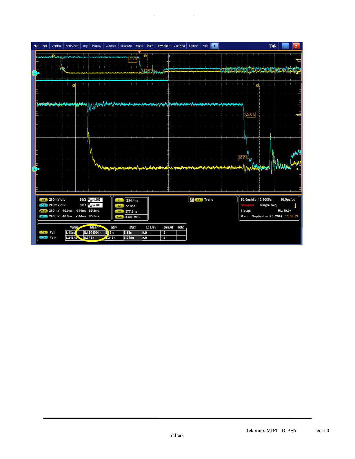
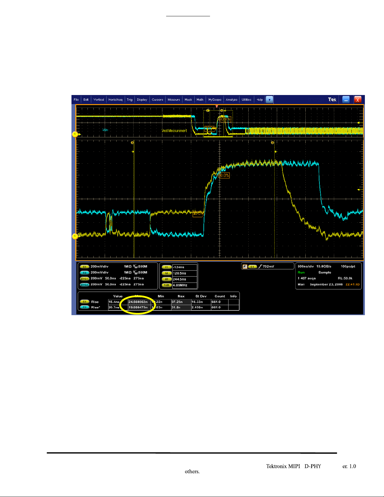
Test 1.3.11 – Data Lane HS TX 20%-80% Rise Time (tR)
Purpose: To verify that the 20%-80% Rise Time (tR) of the DUT Data Lane HS transmitter is within the
conformance limits.
References:
[1] D-PHY* Specification, Section 8.1.1, Line 1361
[2] Ibid, Section 8.1.1, Table 17
[3] UNH* D-PHY* Conformance Test Suite, ver0.08, Test 1.3.11
Resource Requirements: Real-time DSO, D-PHY* test signal generator.
Last Modification: October 16, 2009
Discussion [3]:
The D-PHY Specification states, “The rise and fall times, tR and tF, are defined as the transition time
between 20% and 80% of the full HS signal swing. The driver shall meet the tR and tF specifications for all
allowable ZID.” [1].
In this test, a sample of the DUTs HS Data Lane signaling will be captured using a real-time DSO. The
differential waveform VOD will be computed as difference of the positive and negative single-ended
waveforms (VDP-VDN). The average 20%-80% Rise Time (tR) across all HS transitions will be measured relative
to the average VOD(0) and VOD(1) amplitude values determined previously, to produce the final tR result.
The value of tR must be greater than 150 ps and less than 0.3 UI (where UI is the nominal HS Unit
Interval for the DUT) in order to be considered conformant [2].
Test Setup: See Appendix A and B.
Test Procedure:
1. Connect the DUT to the Test System (See Appendix A)
2. Configure the Test System to emulate the DUT link partner (Master or Slave).
3. Create a condition that causes an HS Data Transmission Burst to be sourced from the DUT, and
capture the exchange using the DSO.
4. From the oscilloscope main menu, select Analyze→Jitter and Eye Analysis→Select
5. Recall the setup file “D-PHY_Test_1_3_11_tR_tF.set”.
6. Ensure explicit clock edge is set correctly by going to Configure → Clock Recovery→Advanced.
(How to set this has been shown in the earlier tests).
7. Click on“Run” to compute the rise and fall times on 10K or more edges. Go to Results tab to
view the measured results for rise and fall time.
8. Compare measured results against the limits in the observable results.
Page 48

® *
MOI v
48
*: Other names and brands may be claimed as the property of
Tektronix, Inc.
In this example, UI is measured with the width measurement, showing 1.84 ns. Upper limit is calculated at
.3*1.84 ns=552 ps, and the lower limit is 150 ps, so this device passes the test.
Observable Results:
• Verify that tR is greater than 150ps and less than 0.3UI.
• The UI width can be read from the mean value of the width displayed in the table. Use this value to
calculate .3*UI, and verify that the measured rise and fall times are less than the calculated value.
Note: The Gated Cursor must be adjusted if required and should be placed in between the payload region
as shown in above Figure.
Page 49
® *
MOI v
49
*: Other names and brands may be claimed as the property of
Tektronix, Inc.
Test 1.3.12 – Data Lane HS TX 20%-80% Fall Time (tF)
Purpose: To verify that the 80%-20% Fall Time (tF) of the DUT Data Lane HS transmitter is within the
conformance limits.
References:
[1] D-PHY* Standard, Section 8.1.1, Line 1361
[2] Ibid, Section 8.1, Table 17
[3] UNH* D-PHY* Conformance Test Suite, ver0.08, Test 1.3.12
Resource Requirements: Real-time DSO, D-PHY* test signal generator.
Last Modification: October 16, 2009
Discussion [3]:
The D-PHY Specification states, “The rise and fall times, tR and tF, are defined as the transition time
between 20% and 80% of the full HS signal swing. The driver shall meet the tR and tF specifications for all
allowable ZID.” [1].
Note the procedure for this test is identical to the previous test (see Test 1.3.11), except that the
average
80%-20% Fall Time (tF) is measured.
The value of tF must be greater than 150 ps and less than 0.3 UI (where UI is the nominal HS Unit
Interval for the DUT, see Test 1.4.16) in order to be considered conformant [2].
(Must add test cases to cover ZID requirements.)
Test Setup: See Appendix A and B.
Test Procedure:
1. Connect the DUT to the Test System (See Appendix A)
2. Configure the Test System to emulate the DUT link partner (Master or Slave).
3. Create a condition that causes an HS Data Transmission Burst to be sourced from the DUT, and
capture the exchange using the DSO.
4. Measure tF as described above.
Observable Results:
• Read the value for tF from the data gathered from 1.3.11, and verify the value is greater than 150 ps
and less than 0.3 UI.
Page 50
® *
MOI v
50
*: Other names and brands may be claimed as the property of
Tektronix, Inc.
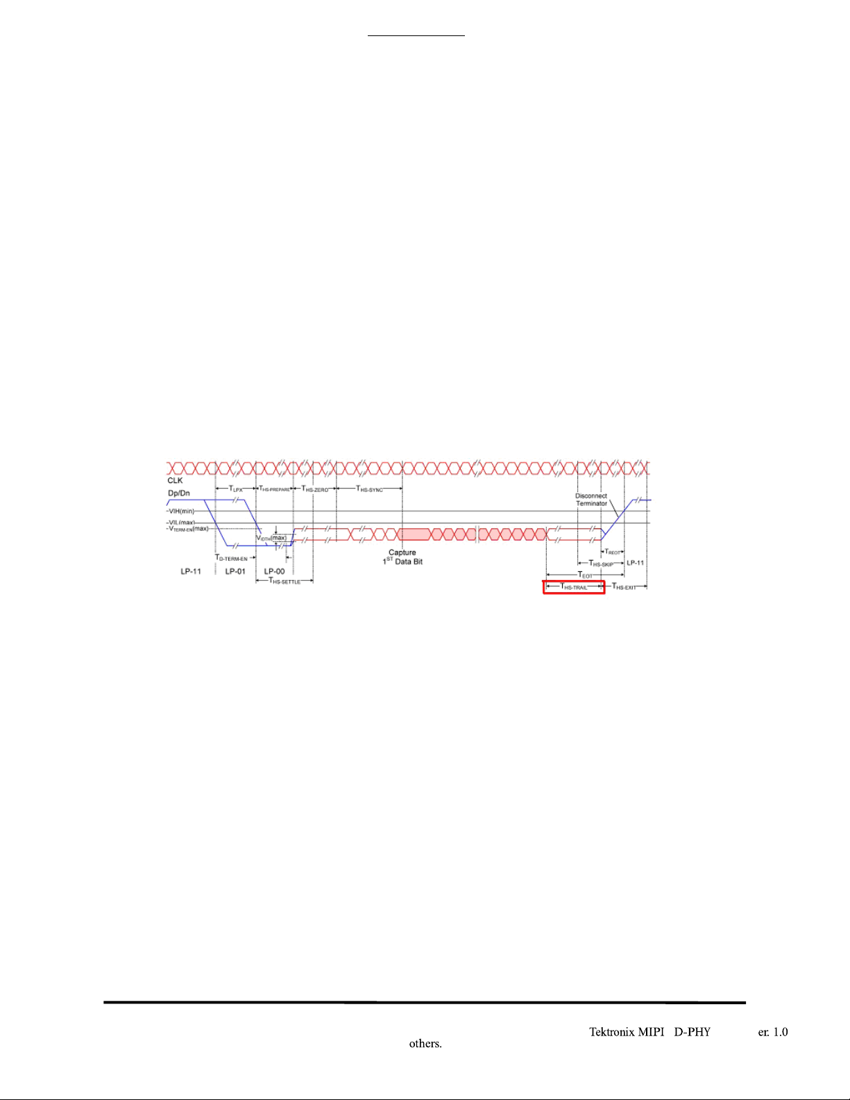
Test 1.3.13 – Data Lane HS Exit: THS-TRAIL Value
Purpose: To verify that the duration the DUT Data Lane TX drives the inverted final differential state following
the last payload data bit of a HS-TX burst (THS-TRAIL), is greater than the minimum required value.
References:
[1] D-PHY* Standard, Section 5.14.2, Line 1031
[2] Ibid, Section 5.9, Table 14
[3] UNH* D-PHY* Conformance Test Suite, ver0.08, Test 1.3.13
Resource Requirements: Real-time DSO, D-PHY* test signal generator.
Last Modification: October 16, 2009
Discussion [3]:
As part of the process of completing a HS Data Transmission Burst, the D-PHY Specification provides a
requirement for the length of time that a device must drive the final extended HS differential state
following the last payload data bit of a HS transmission burst. This interval is defined as THS-TRAIL, and
is shown in the figure below.
Figure: THS-TRAIL Interval
After transmitting the final payload data bit of a HS Data Transmission Burst, the final extended HS
differential state shall be held for a minimum duration of (n*8*UI) or (60 ns + n*4*UI), whichever is greater
(where n = 1 for Forward-direction HS mode, and n = 4 for Reverse-direction HS mode).
In this test, an HS-TX Data Lane signaling burst from the DUT transmitter will be captured using a real-
time DSO. The differential waveform VOD will be computed as difference of the positive and negative
single-ended waveforms (VDP-VDN). The THS-TRAIL interval will be measured for the final extended HS
differential state, at the points where VOD enters and exits the minimum valid HS-RX differential range (i.e,
when VOD crosses +70 or -70 mV). The measured THS-TRAIL result should be greater than max ((n*8*UI), (60
ns + n*4*UI)) to be considered conformant [2].
Test Setup: See Appendix A and B.
Test Procedure:
1. Connect the DUT to the Test System (See Appendix A).
2. Recall setup file “D-PHY_Test_1_3_13_tHS_trail.set”. Press single to get to the desired part of
the signal.
Note: Click on Multiview Zoom if you do not see the zoom area.
3. Ensure that the cursors apply to the area of the signal as shown in the diagram above.
4. Note the ∆t value as the value of THS-TRAIL.
Page 51

® *
MOI v
51
*: Other names and brands may be claimed as the property of
Tektronix, Inc.
5. Repeat for each data lane.
Page 52
® *
MOI v
52
*: Other names and brands may be claimed as the property of
Tektronix, Inc.
Observable Results:
• Verify that THS-TRAIL is greater than max ((n*8*UI), (60 ns + n*4*UI)), for each Data Lane.
Page 53

® *
MOI v
53
*: Other names and brands may be claimed as the property of
Tektronix, Inc.
Test 1.3.14 – Data Lane LP TX: 30%-85% Post-EoT Rise Time (TREOT)
Purpose: To verify that the 30%-85% Post-EoT Rise Time (TREOT) of the DUT LP Data Lane transmitter is within
the conformance limits.
References:
[1] D-PHY* Standard, Section 8.1.2, Line 1417
[2] Ibid, Section 8.1.2, Table 19
[3] UNH* D-PHY* Conformance Test Suite, ver0.08, Test 1.3.14
Resource Requirements: Real-time DSO, D-PHY* test signal generator.
Last Modification: October 16, 2009
Discussion [3]:
The D-PHY Specification states, “The rise-time of TREOT starts from the HS common-level at the
moment the differential amplitude drops below 70 mV, due to stopping the differential drive.” [1].
Figure: TREOT Rise Time
In this test, an HS-TX Data Lane signaling burst from the DUT transmitter will be captured using a real-
time DSO. The differential waveform VOD will be computed as difference of the positive and negative
single-ended waveforms (VDP-VDN). The TREOT Rise Time will be measured starting at the time where VOD
last crosses +/- 70 mV, and ends where VDP crosses VIH,MIN = 880 mV. (Note that the spec does not
differentiate whether VDP or VDN should be used, as they are identical from the spec’s perspective. However,
for real devices the rise times may not be the same, and it may make a difference.)
The value of TREOT shall be less than 35 ns in order to be considered conformant [2].
Test Setup: See Appendices A and B.
Test Procedure:
1. Connect the DUT to the Test System (See Appendix B).
2. Configure the Test System to emulate the DUT link partner (Master or Slave).
3. Create a condition that causes a HS Data Transmission Burst to be sourced from the DUT and
capture the exchange using the DSO.
4. Load the setup file named D-PHY_Test_1_3_14_tREOT.set. Press Single to reach the desired
part of the signal.
5. Cursors are set so that a min and a max of the waveform are between them and so that the
edge to be measured is between them as shown in screen shot below.
6. Read out the Rise time measurements from Ch1 and Ch2.
Page 54
® *
MOI v
54
*: Other names and brands may be claimed as the property of
Tektronix, Inc.
7. Watch out for: If the HS signal is at a high at the time of transition to low power high then this
may be very close to the 30% level and noise may periodically result in incorrect rise time
measurement that is too long. To check for this go to the Measurement Setup menu as shown
in the fixture below and select Annotation marker arrows on the screen indicate at which the
measurement is taken. If the arrows periodically jump then that is observable. This is only
likely if the HS starts from a high level rather than from a low level.
Observable Results:
• Verify that TREOT is less than 35 ns, for each Data Lane.
Page 55

® *
MOI v
55
*: Other names and brands may be claimed as the property of
Test Name
Setup File
Test 1.4.1 – Clock Lane HS Entry: Data Lane TLPX Value
D-PHY_Test_1_4_1_tLPX.set
Test 1.4.2 – Clock Lane HS Entry: THS-PREPARE Value
D-PHY_Test_1_4_2_tHSprep.set
Test 1.4.3 – Clock Lane HS Entry: THS-PREPARE + THS-ZERO Value
D-PHY_Test_1_4_3_tHSp_tHs0.set
Test 1.4.4 – Clock Lane HS TX Differential Voltage (VOD)
D-PHY_Test_1_4_4_Vod.set
Test 1.4.5 – Clock Lane HS TX Differential Voltage Mismatch (∆VOD)
D-PHY_Test_1_4_4_Vod.set
Test 1.4.6 – Clock Lane HS TX Single-Ended Output High Voltage (VOHHS)
D-PHY_Test_1_4_6_Voohs.set
Test 1.4.7 - Clock Lane HS TX Static Common mode Voltage(VCMTX)
D-PHY_Test_1_4_7_Vcmtx.set
Test 1.4.8 – Clock Lane HS TX VCMTX Mismatch (∆VCMTX(1,0))
D-PHY_Test_1_4_7_Vcmtx.set
Test 1.4.9 – Clock Lane HS TX Common-Level Variations Between 50-450
MHz (VCMTX(LF))
D-PHY_Test_1_4_9_VcmtxLF.set
Test 1.4.10 – Clock Lane HS TX Common-Level Variations Above 450 MHz
(VCMTX(HF))
D-PHY_Test_1_4_10_VcmtxHF
Test 1.4.11 – Clock Lane HS TX 20%-80% Rise Time (tR)
D-PHY_Test_1_4_11_tR_tF.set
Test 1.4.12 – Clock Lane HS TX 20%-80% Fall Time (tF)
D-PHY_Test_1_4_11_tR_tF.set
Test 1.4.13 – Clock Lane HS Exit: THS-TRAIL Value
D-PHY_Test_1_4_13_tHS_trail.set
Test 1.4.14 – Clock Lane HS Exit: 30%-85% Post-EoT Rise Time (TREOT)
D-PHY_Test_1_4_14_tREOT.set
Tektronix, Inc.
GROUP 4: Clock Lane HS TX ELECTRICAL TESTS
Overview:
This group of tests verifies the High Speed TX electrical requirements of the clock lane as defined in the
D-PHY* Standard.
All the Measurements in group 4 are similar to the measurements in Group 3, except that group 4 uses the
clock lanes instead of the data lanes. So connect the Differential clock lane from the DUT(Vcp, Vcn) to the
scope channels (Ch3 , Ch4) respectively.
The Table below gives the setups used for these group4 measurements
Page 56
® *
MOI v
56
*: Other names and brands may be claimed as the property of
Tektronix, Inc.
GROUP 5: HS-TX CLOCK-TO-DATA LANE TIMING REQUIREMENTS
Overview:
This group of tests verifies various requirements regarding Clock Lane to Data Lane timing.
Status:
These tests have been performed manually as per the conformance requirements. All tests listed by the
UNH* Conformance Test Suite ver 0.08 are present here.
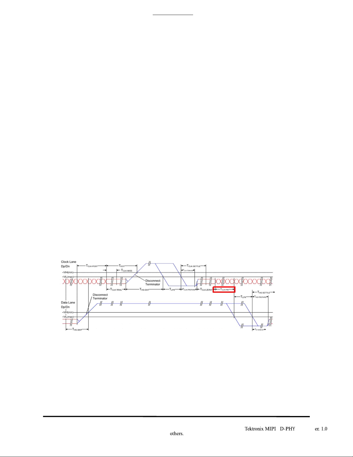
Test 1.5.1 – HS Entry: TCLK-PRE Value
Purpose: To verify that the time that the HS clock is driven prior to an associated Data Lane beginning the
transition from LP to HS mode (TCLK-PRE), is greater than the minimum required value.
References:
[1] D-PHY* Standard, Section 5.14.1, Line 1013
[2] Ibid, Section 5.9, Table 14
[3] UNH* D-PHY* Conformance Test Suite, ver0.08, Test 1.5.1
Resource Requirements: Real-time DSO, D-PHY* test signal generator.
Last Modification: October 16, 2009
Discussion [3]:
As part of the process for initiating an HS data burst transmission, the D-PHY Specification provides a
requirement for the minimum duration that the Master must transmit valid HS Clock signaling before driving
any Data Lane out of LP mode. (Note that this test is only applicable to Master DUTs that support LP capability
on the Clock Lane). This interval is defined as TCLK-PRE, and is shown in the figure below.
Figure: TCLK-PRE Interval
In this test, the DUT will be configured to send an HS burst sequence, and the TCLK-PRE value will be
observed. The TCLK-PRE interval is measured from the end of the Clock Lane TCLK-ZERO interval (at the point
where VOD crosses below the minimum valid HS-RX differential threshold level of +/-70 mV) to the point
where the Data Lane’s VDP LP-01 falling edge crosses VIL,MAX (550 mV).
The measured value of TCLK-PRE shall be be greater than 8*UI in order to be considered conformant
[2]
Test Setup: See Appendix A.
Page 57
® *
MOI v
57
*: Other names and brands may be claimed as the property of
Test Procedure:
1. Connect the DUT to the Test Setup.
2. Create a condition that causes the DUT to source a Clock Lane/Data Lane 0 HS burst sequence.
3. Recall setup file D-PHY_Test_1_5_1_tCLKPre.set.
4. Press Single button to reach the desired portion of the signal. Apply cursors as shown in the
5. Measure ∆t as the TCLK-PRE.
6. Repeat the previous steps for Data Lanes 1, 2, and 3 (if DUT implements multiple Data
Tektronix, Inc.
diagram above.
Lanes).
Observable Results:
• Verify that TCLK-PRE is greater than 8*UI for each Data Lane.
Test 1.5.2 – HS Exit: TCLK-POST Value
Purpose: To verify that the DUT Clock Lane HS transmitter continues to transmit clock signaling for the
minimum required duration (TCLK-POST) after the last Data Lane switches to LP mode.
References:
[1] D-PHY* Standard, Section 5.7, Line 920
Page 58

® *
MOI v
58
*: Other names and brands may be claimed as the property of
Tektronix, Inc.
[2] Ibid, Section 5.9, Table 14
[3] UNH* D-PHY* Conformance Test Suite, ver0.08, Test 1.5.2
Resource Requirements: Real-time DSO, D-PHY* test signal generator.
Last Modification: October 16, 2009
Discussion [3]:
As part of the process for completing an HS data burst transmission, the D-PHY Specification provides a
requirement for the minimum duration that the Master must continue to transmit HS Clock signaling after the
last Data Lane has switched to LP mode [1]. (Note this test is only applicable to Master DUT’s that support LP
capability on the Clock Lane). This interval is defined as TCLK-POST, and is shown in the figure below.
Figure: TCLK-POST Interval
In this test, the DUT will be configured to send an HS burst sequence, and the TCLK-POST value will be
observed. The TCLK-POST interval is measured from the end of the Data Lane THS-TRAIL period to the start of
the Clock Lane TCLK-TRAIL period.
The measured value of TCLK-POST shall be greater than (60 ns + 52*UI) ns in order to be considered
conformant[2].
Test Setup: See Appendix A and B.
Test Procedure:
1. Connect the DUT to the Test Setup.
2. Create a condition that causes the DUT to source a Clock Lane/Data Lane 0 HS burst sequence.
3. Recall setup file D-PHY_Test_1_5_2_tClkpost.set. Use Zoom to find the area to place the
cursors.
4. Press Single button to reach the desired portion of the signal. Apply cursors as shown in the
diagram above.
5. Measure ∆t as the TCLK-POST.
Page 59

® *
MOI v
59
*: Other names and brands may be claimed as the property of
Tektronix, Inc.
Observable Results:
• Verify that TCLK-POST is greater than (60 ns + 52*UI) ns for each Data Lane.
Page 60

® *
MOI v
60
*: Other names and brands may be claimed as the property of
Tektronix, Inc.
Test 1.5.3 – HS Clock Rising Edge Alignment to First Payload Bit
Purpose: To verify that the DUT HS Clock is properly aligned to the payload data signaling.
References:
[1] D-PHY* Standard, Section 9.2, Line 1575
[2] UNH* D-PHY* Conformance Test Suite, ver0.08, Test 1.5.3
Resource Requirements: Real-time DSO, D-PHY* test signal generator.
Last Modification: October 16, 2009
Discussion [2]:
The D-PHY Specification states, “The transmitter shall ensure that a rising edge of the DDR clock is sent
during the first payload bit of a transmission burst such that the first payload bit can be sampled by the
receiver on the rising clock edge, the second bit can be sampled on the falling edge, and all following bits can
be sampled on alternating rising and falling edges.” [1].
In this test, the DUT will be configured to send an HS burst sequence, and the Clock and Data Lane
signals will be observed using a real-time DSO. The signaling behavior will be visually examined to verify that
the first payload bit of a transmission burst aligns with a rising edge of the DDR clock.
Test Setup: See Appendix A and B.
Test Procedure:
• Connect the DUT to the Test Setup.
• Create a condition that causes the DUT to source a Clock Lane/Data Lane 0 HS burst sequence.
• Recall setup file D-PHY_Test_1_5_3_talign.set. Press Single for getting to the desired part of the signal.
• Using oscilloscope cursors, find the direction of the DDR clock edge that corresponds to the first Data
Lane payload bit of the transmission burst (i.e,, rising or falling).
• Repeat the previous steps for Data Lanes 1, 2, and 3 (if DUT implements multiple Data Lanes).
Page 61

® *
MOI v
61
*: Other names and brands may be claimed as the property of
Tektronix, Inc.
Observable Results:
• The first Data Lane payload bit of the transmission burst should align with a rising edge of the DDR
clock for each Data Lane.
Page 62

® *
MOI v
62
*: Other names and brands may be claimed as the property of
Tektronix, Inc.
Test 1.5.4 – Data-to-Clock Skew (TSKEW(TX))
Purpose: To verify that the skew between the clock and data signaling, as measured at the transmitter
(TSKEW(TX)) is within the conformance limits.
References:
[1] D-PHY* Standard, Section 9.2.1, Line 1589
[2] UNH* D-PHY* Conformance Test Suite, ver0.08, Test 1.5.3
Resource Requirements: Real-time DSO, D-PHY* test signal generator.
Last Modification: October 16, 2009
Discussion [2]:
The specification states, “The skew specification, TSKEW[TX], is the allowed deviation of the data launch
time to the ideal ½UIINST displaced quadrature clock edge.”[1]. This relationship is graphically
demonstrated via a figure in the specification, which is reproduced in the figure below.
Figure: TSKEW(TX) Definition
In this test, the DUT will be configured to send an HS burst sequence, and the Clock and Data Lane signals will
be observed using a real-time DSO. The timing error between each Data Lane edge and its respective Clock
Lane edge will be computed, to produce an array of timing error values. The max, min, and mean timing error
values measured across all observed edges will be recorded.
Test Setup: See Appendix A and B.
Test Procedure:
1. Connect the DUT to the Test Setup.
2. Create a condition that causes the DUT to source a Clock Lane/Data Lane 0 HS burst sequence.
3. Launch DPOJET using the main menu: Analyze → Jitter and Eye Analysis.
4. Recall the setup file D-PHY_Test_1_5_4_tskewTx.set.
5. Apply the explicit clock recovery as detailed in the previous tests.
Page 63

® *
MOI v
63
*: Other names and brands may be claimed as the property of
Tektronix, Inc.
6. Click Run.
7. Record the max, min, and mean timing error values from the results as given in the table.
8. Compare with the compliance requirement between 0.65UIINST and 0.35UIINST.
9. Repeat the previous steps for Data Lanes 1, 2, and 3 (if the DUT implements multiple Data Lanes).
Page 64
® *
MOI v
64
*: Other names and brands may be claimed as the property of
Tektronix, Inc.
Observable Results:
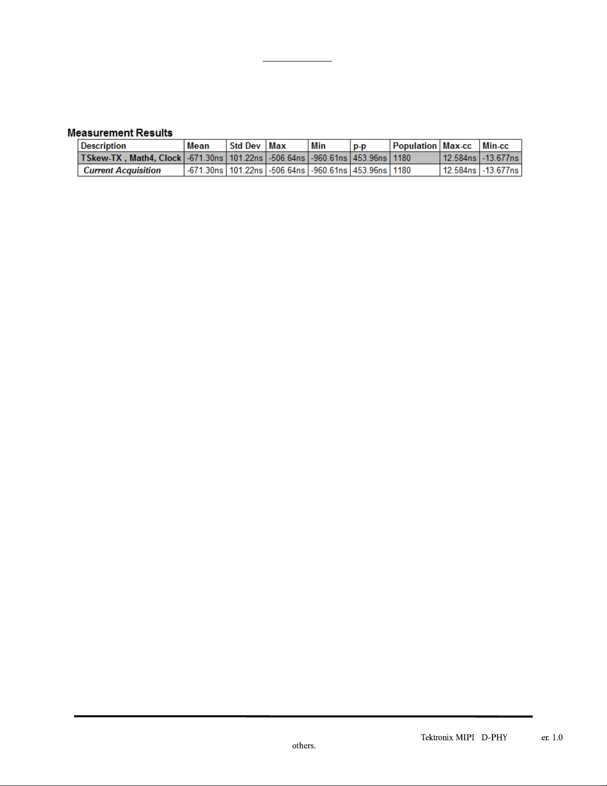
• Verify that the max, min, and mean Clock-to-Data timing error values are within the range (0.50
±0.15)*UIINST, for each Data Lane.
Page 65

® *
MOI v
65
*: Other names and brands may be claimed as the property of
Tektronix, Inc.
GROUP 6: LP-TX INIT, ULPS, AND BTA REQUIREMENTS
Overview:
This group of tests verifies several miscellaneous LP-TX timing and behavioral requirements pertaining
to initialization (INIT), Ultra-Low Power State (ULPS) and Bus Turnaround (BTA).
Status:
These tests have been performed manually as per the conformance requirements. All tests listed by the
UNH* Conformance Test Suite ver 0.08 are present here.
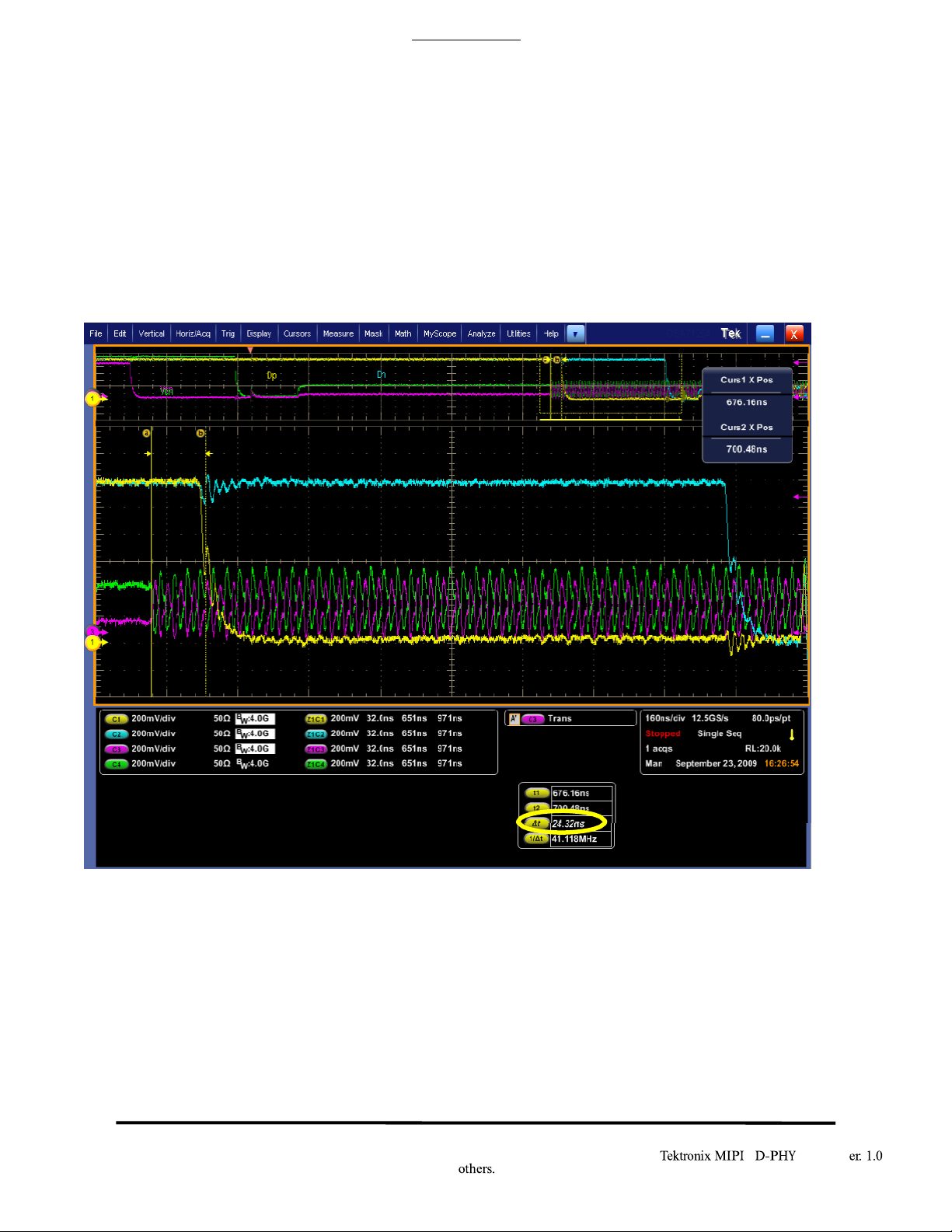
Test 1.6.3 – ULPS Exit: Transmitted TWAKEUP Interval
Purpose: To verify that the DUT transmits Mark-1 for the proper duration (TWAKEUP) when initiating a Clock or
Data Lane ULPS Exit sequence.
References:
[1]. D-PHY* Standard, Section 5.6.3, Line 895
[2]. Ibid, Section 5.8, Line 951
[3]. UNH* D-PHY* Conformance Test Suite, ver1.0, Test 1.6.3
Resource Requirements: Real-time DSO, D-PHY* test signal generator.
Last Modification: July 14, 2011
Discussion [3]:
A typical Ultra Low Power State (ULPS) transmission consists of an escape mode entry(LP11, LP10, LP00, LP01
and LP00), ULPS entry command pattern(00011110), ULPS data(LP00) followed by a MARK-1(LP10) and a stop
state(LP11).
Below screen shot shows the ULPS transmission.
The D-PHY Specification defines a mechanism for bringing Lanes out of the ULPS state. This process involves
driving a Mark-1 state (LP-10) for a minimum time TWAKEUP, followed by a Stop state (LP-11), which should be
detected by the Slave device. (Note that this test is only applicable to Master DUTs.)
The purpose of this test is to verify that a DUT transmits Mark-1 for the minimum required duration when
initiating a ULPS exit on either a Clock or Data Lane. Note that the termination environment is not critical to this
measurement, and either the CLOAD fixture, RTB, or no termination fixture may be used. The DUT will be
instructed to put both the Clock and Data Lanes into ULPS mode, and then subsequently initiate a ULPS exit,
allowing the Mark-1 duration to be observed.
TWAKEUP is measured from the start of the Mark-1 state (at the point where the Dp line of LP-10 transition
crosses VIH,MIN = 880mV), to the start of the Stop state (at the point where the Dn line of LP-11 transition
crosses VIH,MIN = 880mV).
The measured TWAKEUP value should be greater than or equal to 1ms.
Page 66
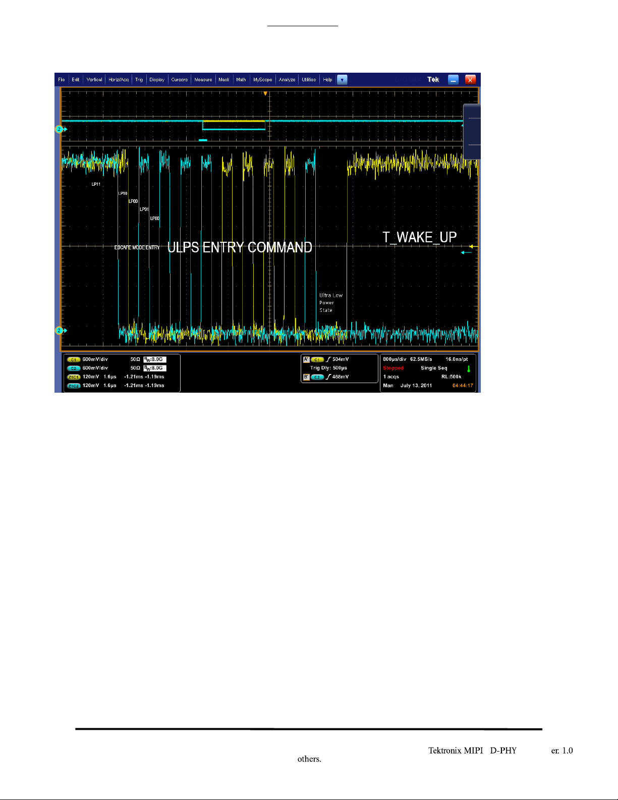
® *
MOI v
66
*: Other names and brands may be claimed as the property of
Tektronix, Inc.
Test Setup: See Appendix A.
Test Procedure:
1. Connect the DUT to the test setup.
2. Create a condition that causes DUT to enter and exit ULPS state repeatedly
3. Recall setup file D_PHY_Test_1_6_3.set
4. Press single button to reach the desired portion of the signal. Refer the screen shot given below.
Zoom 1 shows the start of TWAKEUP and zoom 2 shows the end of TWAKEUP. Apply cursors as
shown in the screen shot below.
5. Measure Δt as the TWAKEUP.
Page 67

® *
MOI v
67
*: Other names and brands may be claimed as the property of
Tektronix, Inc.
Observable Results:
Verify that TWAKEUP is greater than or equal to 1ms.
Test 1.6.4 – BTA: TX-Side TTA-GO Interval Value
Purpose: To verify that the DUT drives the Bridge state(LP-00) for the proper period(TTA-GO), when handing off
control of the link during Link Turnaround procedure.
References:
[4]. D-PHY Specification, Section 5.9, Table 14
[5]. Ibid, Section 5.8, Line 951
[6]. UNH* D-PHY* Conformance Test Suite, ver1.0, Test 1.6.4
Resource Requirements: Real-time DSO, D-PHY* test signal generator.
Last Modification: Sept 14, 2011
Discussion [3]:
The link Turnaround process consists of a LP handshake/handoff procedure between the Master and Slave sides
of the link. The controlling device initiates the handoff process by signaling Stop/LP-Rqst/Bridge/LP-Rqst/Stop
(LP11/10/00/10/00). The receiving device then assumes control of the link, simultaneously driving the Bridge
Page 68
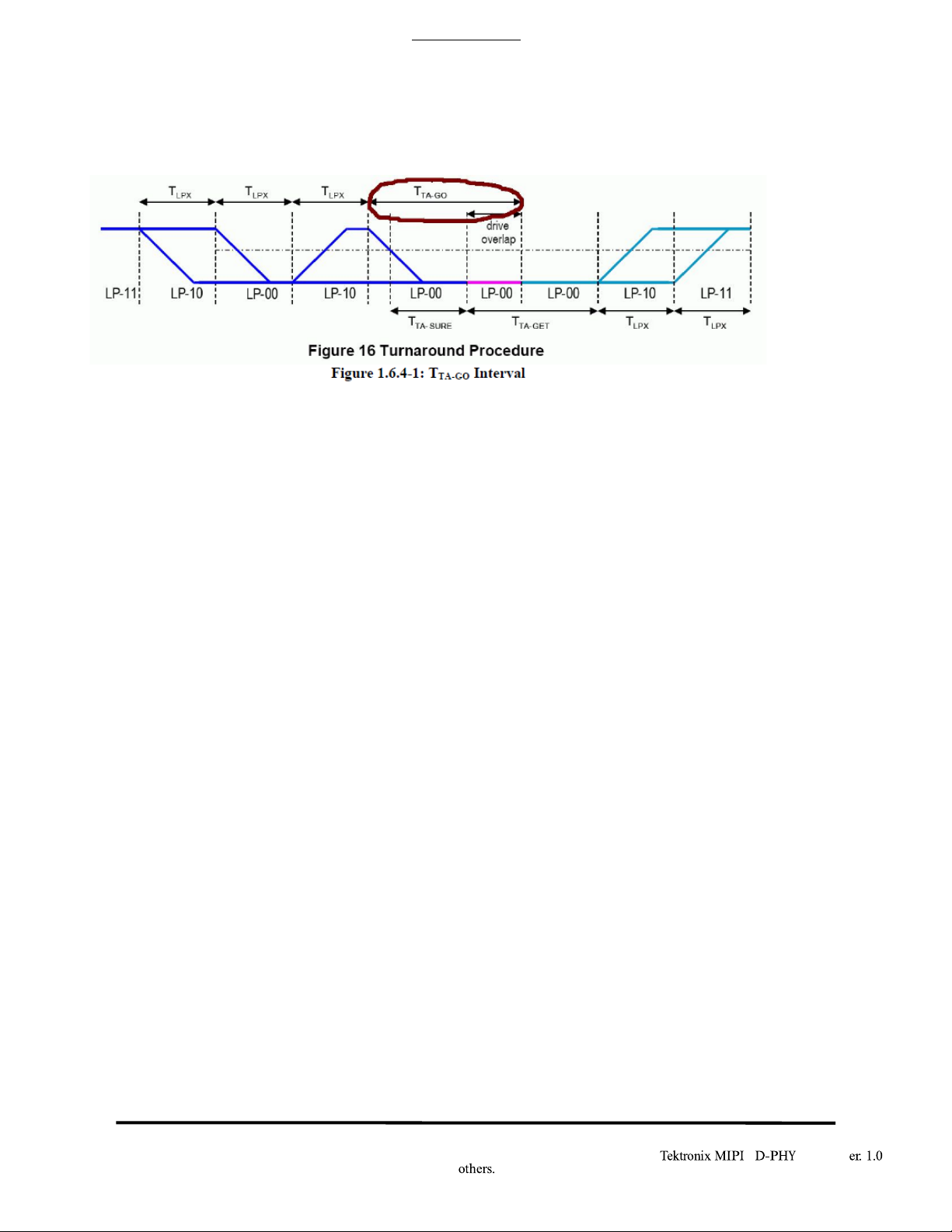
® *
MOI v
68
*: Other names and brands may be claimed as the property of
Tektronix, Inc.
state (LP-00), followed by its own LP-Rqst and Stop states (LP-10/11), after which the transfer process is
considered complete. A complete picture of the entire Turnaround procedure (reproduces from Figure 16 of the
DPHY specification), which shows the TTA-GO interval is shown below.
The specification defines TTA-GO as the “Time that the transmitter drives the Bridge state(LP-00) before
releasing control during a link turnaround. Therefore the TTA-GO period begins at the start of the last TX-side
LP-00 state and ends when the TX-side device ceases transmission.
If the exact point cannot be observed, an alternative methodology would require measuring the entire time
interval from the end of the last TX-side LP10 to the beginning of the first RX-side LP10, then subtracting one
nominal RX-side TLPX interval. Remaining value would be TTA-GO.
The specification states that TTA_GO must be greater than or equal to 4*TLPX ns in order to be considered
conformant, where TLPX is the average LP state duration of the DUT.
Test Setup: See Appendix A.
Test Procedure:
1. Create a setup with two MIPI DPHY DUTs, one acting as master and other one acting as a slave.
2. Connect the master DUT to the test setup.
3. Create a condition that causes master DUT to enter the link turnaround process.
4. Recall setup file DPHY_TLPX.set.
Page 69

® *
MOI v
69
*: Other names and brands may be claimed as the property of
Tektronix, Inc.
5. Press single button to reach the desired portion of the signal. Refer the screen shot given below.
Page 70

® *
MOI v
70
*: Other names and brands may be claimed as the property of
Tektronix, Inc.
6. Measure the TLPX duration(LP State duration with 550 mV as reference). Refer the below screen
shot for zoomed TLPX region.
7. Recall setup file DPHY_TX_1_6_4.set. Make sure in the trigger setup, the lower limit for width
trigger on Ch1 is greater than two times the measured TLPX duration. Refer the screen shot below.
Page 71

® *
MOI v
71
*: Other names and brands may be claimed as the property of
Tektronix, Inc.
8. Press single button to reach the desired portion(Link Turn around) of the signal. Refer the screen
shot given below(zoomed link turn around region).
9. Measure Δt. TTA_GO is given as (Δt - TLPX).
Page 72
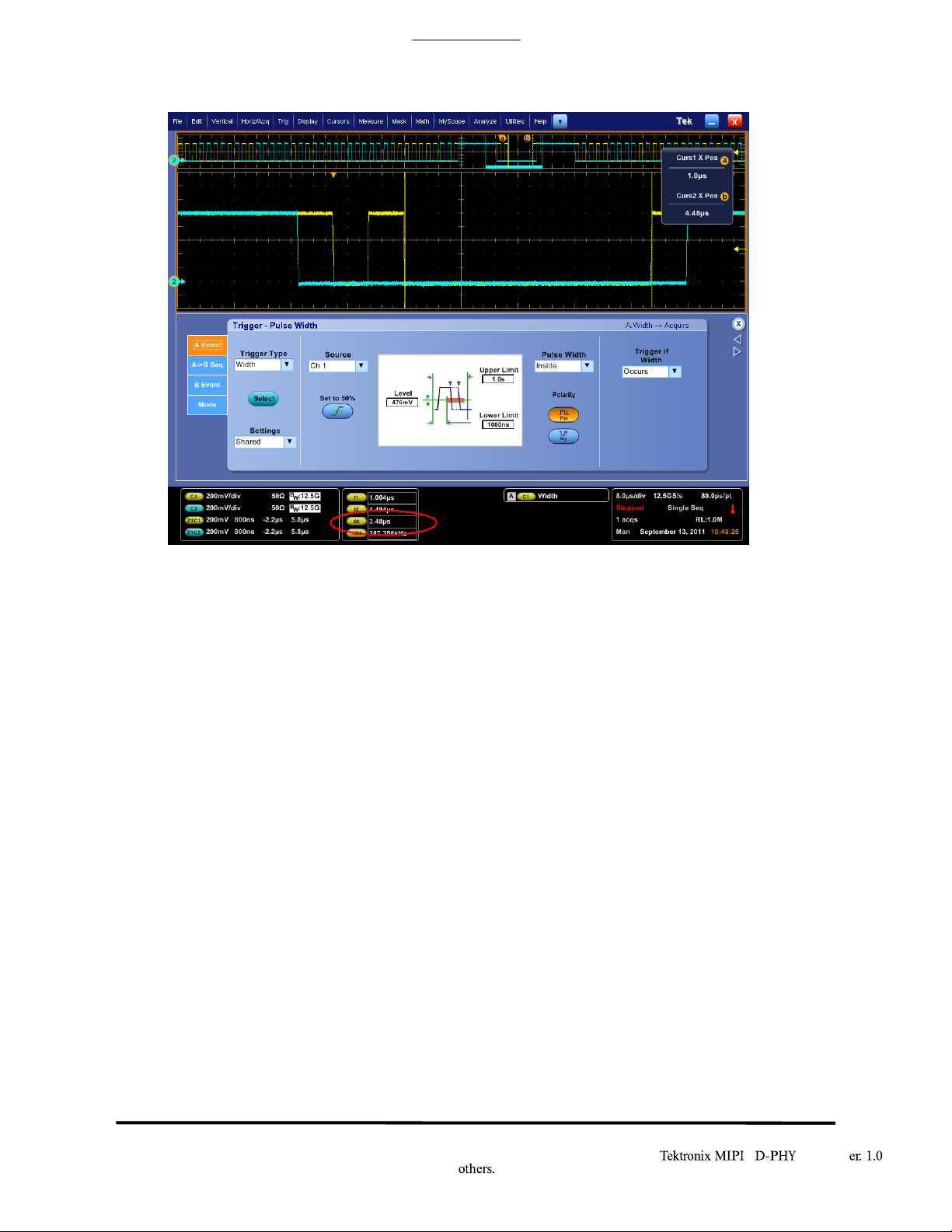
® *
MOI v
72
*: Other names and brands may be claimed as the property of
Tektronix, Inc.
Observable Results:
Verify that TTA_GO is greater than or equal to (4*TLPX).
Page 73

® *
MOI v
73
*: Other names and brands may be claimed as the property of
Tektronix, Inc.
Appendix A – Resource Requirements
The resource requirements include two separate sets of equipment. A.1 Equipment for D-PHY* tests
1. Real-time Digital Oscilloscope (any one of the following instruments)
1 Qty DPO7354, or DPO/DSAMSO70404B/C/D or higher bandwidth Oscilloscope
2. Software
DPOJET Advanced (Option DJA) enabled with Option D-PHY- D-PHY Essentials.
3. Probes (Any one of the following probe sets)
4 Qty P7240/ TAP3500/ P6245/ P6249/ TDP3500/ P73xx.
4. (4) Matched Pair SMA Cables
5. (4.) TCA-292MM or TCS-SMA
6. Optional: D-PHY Termination Board & Probing Board from University of New Hampshire
Interoperability lab (UNH-IOL)
– www.iol.unh.edu/services/testing/mipi/fixtures.php
– www.iol.unh.edu/services/testing/mipi/MIPI_Test_Fixture_Order_Form.doc
7. For up-to-date configuration details, browse to www.tektronix.com/MIPI
Page 74

® *
MOI v
74
*: Other names and brands may be claimed as the property of
Tektronix, Inc.
Appendix B – DUT Connection
Make connections as follows for single-ended tests:
Page 75

® *
MOI v
75
*: Other names and brands may be claimed as the property of
Tektronix, Inc.
Make connections as follows for differential tests:
Page 76

® *
MOI v
76
*: Other names and brands may be claimed as the property of
Tektronix, Inc.
Appendix C – Deskew Procedure
Deskew for SMA Channels
The following is a procedure that can be used for de-skewing direct input SMA channels on an oscilloscope.
This procedure is useful for any Tektronix real-time oscilloscope, using either SMA or 292mm inputs.
1. Run SPC on the oscilloscope.
2. Connect an SMA Power Splitter (preferred) or SMA 50 ohm coax tee to the Fast Edge output of the
oscilloscope.
3. Connect SMA cables from each of the two channels to be de-skewed, to the power splitter (or SMA
coax tee). It is best to use matched cables when making high speed serial measurements. It is critical to
use the same cables that will be used for subsequent measurements.
4. Press Default Setup, then Autoset on oscilloscope front panel.
5. Set oscilloscope for 70%-90% full screen amplitude on both channels. Center both traces to overlap.
6. Make sure that volts/div, position, and offset are identical for the two channels being de-skewed.
7. Set time/div to approx. 100 ps/div or less, with sample rate at 1 ps/pt. These settings are not critical,
but should be close.
8. Set horizontal acquisition mode to average, which provides a more stable display.
9. Select Deskew from the Vertical menu.
10. Verify ref channel (typically Ch1 or Ch2) is set to 0 ps deskew.
11. In the deskew control window, click on channel to deskew (typically Ch3 or Ch4). Adjust deskew to
overlay rising edge as best possible.
Note: Typical values are in the 10’s of ps or less with cables connected directly from Fast Edge to SMA
inputs. If you are using an RF relay switch box (e.g. Keithley), deskew the complete path from where the
test fixture connects, through the switch, and into the oscilloscope. Deskew values in these cases may be
as much as
30ps or more.
There are sometimes significant differences in skew between two TCA-SMA adapters. If you find that a
system requires very large correction, it might be better to find a pair of TCA-SMA adapters that match
each other better.
Do not forget to set the oscilloscope back to default settings when done. Otherwise, the horizontal
averaging will likely to give incorrect results.
 Loading...