

Page 1

xx
MDO4000 Series
Mixed Domain Oscilloscopes
ZZZ
Specifications and Performance Verification
Technical Reference
*P077058301*
077-0583-01
Page 2

Page 3

xx
MDO4000 Series
Mixed Domain Oscilloscopes
ZZZ
Specifications and Performance Verification
Technical Reference
This document supports firmware version 2.94 and above for
MDO4000 Series instruments.
Warning
The servicing instructions are for use by qualified personnel
only. To avoid personal injury, do not perform any servicing
unless you are qualified to do so. Refer to all safety summaries
prior to performing service.
Revision A
www.tektronix.com
077-0583-01
Page 4

Copyright © Tektronix. All rights reserved. Licensed software products are owned by Tektronix or its subsidiaries
or suppliers, and are protected by national copyright laws and international treaty provisions.
Tektronix products are covered by U.S. and foreign patents, issued and pending. Information in this publication
supersedes that in all previously published material. Specifications and pric e change privileges reserved.
TEKTRONIX and TEK are registered trademarks of Tektronix, Inc.
Contacting Tektronix
Tektronix, Inc.
14150 SW Karl Braun Drive
P.O . B ox 5 0 0
Beaverto
USA
For product information, sales, service, and technical support:
n, OR 97077
In North America, call 1-800-833-9200.
World wi de, vis i t www.tektronix.com to find contacts in your area.
Page 5

Table of Contents
General safety summary .............. ................................ ................................ ............ iii
Specifications .................... ................................ .................................. ................. 1
Analog Signal Acquisition System Specifications .................... .................................. ... 1
Time Base System Specifications ............................................................................ 8
Triggering System Specifications ........................................................................... 10
Digital Acquisition System Specifications................................................................. 15
P6616 Digital Probe Input Specifications .................... ................................ .............. 16
RF Input Specifications .... .................................. ................................ ................ 17
Display System Specifications .................... ................................ .......................... 20
Interfaces and Input/Output Port Specifications........................................................... 21
Data Handling Specifications................ ................................ ................................ 22
Power Supply System Specifications ....................................................................... 22
Environmental Specifications ............................................................................... 23
Mechanical Specifications ................................................................................... 24
TPA-N-PRE Specifications ................ ................................ ................................ .. 25
Performance Verification ........... ................................ ................................ .............. 27
Test Record .................. .................................. ................................ ................ 29
Performance Verification Procedures ............................... .................................. ...... 61
Self Test................................................................................................... 62
Check Input Impedance (Resistance) .................................................................. 63
Check DC Balance....................................................................................... 65
Check DC Gain Accuracy............................................................................... 67
Check Offset Accuracy.................................................................................. 71
Check Analog Bandwidth............................................................................... 73
Check Random Noise, Sample Acquisition Mode ... ... . ... . ... ... . ... . ... ... . ... . ... ... . ... . ... . . .. 76
Check Sample Rate and Delay Time Accuracy......................................... .............. 78
Check Delta Time Measurement Accuracy ....................... ................................ .... 80
Check Digital Threshold Accuracy ........ ................................ ............................ 82
Check Phase Noise................................... ................................ .................... 85
Check Displayed Average Noise Level (DANL)..................................................... 88
Check Level Measurement Uncertainty ............... ................................ ................ 92
Check Third Order Intermodulation Distortion. ................................ .................... 100
Check Residual Spurious Response.................................. ................................ 104
Check Crosstalk to RF Channel from Analog Channels..... ................................ ...... 105
Check Trigger Out ................... ................................ .................................. 107
With TPA-N-PRE Attached: Check Display Average Noise Level (DANL) ................... 110
MDO4000 Series Specifications and Performance Ve rification i
Page 6

Table of Contents
List of Tables
Table 1: Analog signal acquisition system specifications...................................................... 1
Table 2 : Tim
Table 3: Delta-Time measurement accuracy formula ....... ................................ ................... 9
Table 4: Trigger specifications ................................................................................... 10
Table 5: Digital acquisition specifications ............................ ................................ .......... 15
Table 6: P6616 digital probe input specifications.............. .................................. .............. 16
Table 7: RF input specifications ................................................................................. 17
Table 8 : D
Table 9: Interfaces and Input/Output port specifications.............. ................................ ........ 21
Table 10: Data handling specifications.................... ................................ ...................... 22
Table 11: Power supply system specifications ................................................................. 22
Table 12: Environmental specifications......................................................................... 23
Table 13: Mechanical specifications............................................................................. 24
14: TPA-N-PRE specifications............ ................................ ................................ 25
Table
Table 15: Required equipment ................................................................................... 28
Table 16: Gain expected worksheet ......... ................................ .................................. .. 69
Table 17: Maximum bandwidth frequency worksheet ........................................................ 74
e base system specifications........................................................................ 8
isplay system specifications........................ ................................ .................. 20
ii MDO4000 Series Specifications and Performance Verification
Page 7

General safety summary
General safet
To avoid fire or personal
injury
y summary
Review the fo
this product or any products connected to it.
To avoid potential hazards, use this product only as specified.
Only qualified personnel should perform service procedures.
Use proper power cord. Use only the power cord specified for this product and
certified for the country of use.
Connect and disconnect properly. Do not connect or disconnect probes or test
leads while they are connected to a v oltage source.
Connect and disconnect properly. De-energize the circuit under test before
connecting or disconnecting the current probe.
Ground the product. This product is grounded through the grounding conductor
of the power cord. To avoid electric shock, the grounding conductor must be
connected to earth ground. Before making connections to the input or output
terminals of the product, ensure that the product is properly grounded.
Observe all terminal ratings. To avoid fire or shock hazard, observe all ratings
and markings on the product. Consult the product manual for further ratings
information before making connections to the product.
llowing safety precautions to avoid injury and prevent damage to
Connect the probe reference lead to earth ground only.
Do not apply a potential to any terminal, including the common terminal, that
exceeds the maximum rating of that terminal.
Power disconnect. The power cord disconnects the product from the power source.
Do not block the power cord; it must remain accessible to the user at all times.
Do not operate without covers. Do not operate this product with covers or panels
removed.
Do not operate with suspected failures. If you suspect that there is damage to this
product, have it inspected by qualified service personnel.
Avoid exposed circuitry. Do not touch exposed connections and components when
power is present.
Do not operate in wet/damp conditions.
Do not operate in an explosive atmosphere.
Keep product surfaces clean and dry.
Provide proper ventilation. Refer to the manual's installation instructions for details
on installing the product so it has proper ventilation.
MDO4000 Series Specifications and Performance Ve rification iii
Page 8
General safety summary
Termsinthismanual
Symbols and terms on the
product
These terms may
WARNING. Warning statements identify conditions or practices that could result
in injury or loss of life.
CAUTION. Caution statements identify conditions or practices that could result in
damage to this product or other property.
These terms may appear on the product:
DANGER in
the marking.
WAR NI NG
read the marking.
CAUTIO
The following symbol(s) m ay appear on the product:
appear in this manual:
dicates an injury hazard immediately accessible as you read
indicates an injury hazard not immediately accessible as you
N indicates a hazard to property including the product.
iv MDO4000 Series Specifications and Performance Verification
Page 9

Specifications
This chapter contains specifications for the MDO4000 Series oscilloscopes. All
specifications are guaranteed unless noted as "typical." Typical specifications are
provided for
marked with the
your convenience but are not guaranteed. Specifications that are
symbol are checked in Performance Verification.
All specific
ations apply to all MDO4000 models unless noted otherwise. To meet
specifications, two conditions must first be met:
The oscill
oscope must have been operating continuously for twenty minutes
within the specified operating temperature range. (See Table 12 on page 23.)
You m us t p
erform the Signal Path Compensation (SPC) operation d escribed
instep2oftheSelf Test before evaluating specifications. (Se e page 62, Self
Test.) If the operating temperature changes by more than 10 °C (18 °F), you
must perform the SPC operation again.
Analog Signal Acquisition System Specifications
The following table shows the specifications for the analog signal acquisition
system.
Table 1: Analog signal acquisition system specifications
Characteristic Description
Number of input
channels
Input coupling
Input resistance
selection
put impedance,
In
DC coupled
Input Capacitance,
1M DC coupled,
typical
4 analog channels, digitized simultaneously
DC or AC
1M or 50
250 k (to be selected for performance verification only).
1M 1M ±1%
50
13 pF ± 2 pF
50 ±1%
MDO4104-X VSWR 1.5:1 from DC to 1 GHz, typical
MDO4054-X VSWR 1.5:1 from DC to 500 MHz, typical
MDO4034-3 VSWR 1.5:1 from DC to 350 MHz, typical
MDO4014-3 VSWR 1.5:1 from DC to 100 MHz, typical
MDO4000 Series Specifications and Performance Ve rification 1
Page 10

Specifications
Table 1: Analog signal acquisition system specifications (cont.)
Characteristic Description
Maximum input
voltage
DC Balance
Number of digitized
bits
(coarse)
Sensitivity range (fine)
Sensitivity resolution
(fine), typical
1M 300 V
at the BNC
RMS
Installation Category II
Derate at 20 dB/decade between 4.5 MHz and 45 MHz
Derate 14 dB/decade between 45 MHz and 450 MHz
Above 450 MHz, 5 V
Maximum peak input voltage at the BNC, ±424 V
250 K 75 V
at the BNC
RMS
Installation Category II
Derate at 20 dB/decade between 1.3 MHz and 13 MHz
Derate 10 dB/decade between 13 MHz and 130 MHz
Above 130 MHz, 5 V
Maximum peak input voltage at the BNC, ±106 V
50 5V
with peaks ±20 V (Duty Factor 6.25%)
RMS
Overvoltage trip is intended to protect against overloads that might damage
termination resistors. A sufficiently large impulse might cause damage
regardless of the overvoltage protection circuitry because of the finite time
required to detect and respond.
0.1 div with the input DC coupled, set to 50 termination, and input terminated with 50 BNC terminator
0.2 div at 1 mV/div with the input DC coupled, set to 5 0 termination, and input terminated with 50
BNC terminator
0.2 div with the input DC coupled, set to 1 M termination, and input terminated with 50 BNC terminator
8bits
Displayed vertically with 25 digitization levels (DL) per division, 10.24 divisions dynamic range.
"DL" is the abbreviation for "digitization level." A DL is the smallest voltage level change that can be
resolved by an 8-bit A-D Converter. This value is also known as the least significant bit (LSB).
1MΩ 1 mV/div to 10 V/div in a 1-2-5 sequenceSensitivity range
50 Ω 1 mV/div to 1 V/div in a 1-2-5 sequence
1MΩ
1 m V/div to 5 V/div < –50% to > +50% of selected setting
10 V/div < –50% to 0%
Allows continuous adjustment from 1 mV/div to 10 V/div
50 Ω
1 mV/div to 500 mV/div < –50% to > +50% of selected setting
1 V/div < –50% to 0%
Allows continuous adjustment from 1 mV/div to 1 V/div
1% of current setting
RMS
RMS
.
.
2 MDO4000 Series Specifications and Performance Verification
Page 11

Table 1: Analog signal acquisition system specifications (cont.)
Characteristic Description
DC gain accur
acy
For 50 Ω,1MΩ, and 250 kΩ (250 kΩ checked indirectly):
±1.5%, derated at 0.100%/°C above 30 °C
±2.0%, derated at 0.100%/°C above 30 °C, 1 mV/Div s etting
±3.0% variable gain, derated at 0.100%/°C above 30 °C
Specifications
Offset ranges,
minimum
Position range ±5 divisions
Offset accuracy
Number of waveforms
for average acquisition
mode
DC voltage
measurement
accuracy
average acquisition
mode
Volts/div setting
1 mV/div to 50 mV/div
50.5 mV/div to 99.5 m V/div
100 mV/div to 500 mV/div
505 mV/div to 995 mV/div
1 V/div to 5 V/div
5.05 V/div to 10 V/div
For 50 path, 1 V/div is the maximum vertical setting.
The input signal cannot exceed Max Input Voltage for the 50 input path. Refer to the Max Input Voltage
specification for more information.
±[0.005 × | offset – position | + DC Balance]
Both the position and the constant offset term must be converted to volts by multiplying by the appropriate
volts/div term.
2to512waveforms
Default of 16 waveforms
Measurement type
Average of 16 waveforms ±[DC Gain Accuracy × | reading – (offset -
Delta Volts between any two averages of 16
waveforms acquired with the same oscilloscope
setup and ambient conditions
Offset, position, and the constant offset term must be converted to volts by multiplying by the appropriate
volts/div term.
The basic accuracy specification applies directly to any sample and to the following measurements: High,
Low, Max, Min, Mean, Cycle Mean, RMS, and Cycle RMS. The delta volt accuracy specification applies to
subtractive calculations involving two of these measurements.
The delta volts (difference voltage) accuracy specification applies directly to the following measurements:
Positive Overshoot, Negative Overshoot, Pk-Pk, and Amplitude.
Offset range
1M input 50 input
±1 V ±1 V
±0.5 V ±0.5 V
±10 V ±10 V
±5 V ±5 V
±100 V ±5 V
±50 V Not applicable
DC Accuracy (in Volts)
position) | + offset accuracy + 0.1 division ]
Refer to DC Gain Accuracy for temperature
derating information.
±[DC gain accuracy × | reading | + 0.05 div]
Refer to DC Gain Accuracy for temperature
derating information.
MDO4000 Series Specifications and Performance Ve rification 3
Page 12

Specifications
Table 1: Analog signal acquisition system specifications (cont.)
Characteristic Description
DC voltage
measurement
accuracy
Sample acquisition
mode, typical
Measurement type
Any sample
Delta volts between any two samples acquired
with the same oscilloscope setup and ambient
conditions
Offset, position, and the constant offset term must be converted to volts by multiplying by the appropriate
volts/div term.
DC Accuracy (in volts)
±[DC gain accuracy × | reading – (offset –
position) | + Offset Accuracy + 0.15 div + 0.6 mV]
Refer to DC Gain Accuracy for temperature
derating information.
±[DC gain accuracy × | reading | + 0.15 div +
1.2 mV]
Refer to DC Gain Accuracy for temperature
derating information.
4 MDO4000 Series Specifications and Performance Verification
Page 13

Table 1: Analog signal acquisition system specifications (cont.)
Characteristic Description
Analog bandwidth
selections
Analog
bandwidth, DC
coupled
Lower frequency limit,
AC coupled, typical
Upper frequency limit,
250 MHz bandwidth
limited, typical
MDO4104-6, MDO4104-3, MDO 4054-6, MDO4054-3, MDO4034-3: 20 MHz, 250 MHz, and Full
MDO4014-3: 20 MHz and Full
These limits are for ambient temperature of 30°C and the bandwidth selection set to FULL. Reduce the
upper bandwidth frequency by 1% for each °C above 30°C
Volts/Div setting
50 Ω
1MΩ,typical
With
TPPXX00
10X probes,
typical
< 10 Hz when AC, 1 M coupled
The AC coupled lower frequency limits are reduced by a factor of 10 when 10X passive probes are used.
250 MHz, ±20%, all models except MDO4014-3
MDO4104-X
MDO4054-X
MDO4014-3 1 mV/div — 1 V/div DC to 100 MHz
MDO4104-X
MDO4054-X
MDO4014-3 1 mV/div — 10 V/div DC to 100 MHz
MDO4104-X
(TPP1000
probe)
MDO4054-X
(TPP0500
probe)
(TPP0500)
MDO4014-3
(TPP0500)
5 mV/div — 1 V/div DC to 1.00 GHz
2 mV/div — 4.98 mV/div DC to 350 MHz
1 mV/div — 1.99 mV/div DC to 175 MHz
5 mV/div — 1 V/div DC to 500 MHz
2 mV/div — 4.98 mV/div DC to 350 MHz
1 mV/div — 1.99 mV/div DC to 175 MHz
2 mV/div — 1 V/div DC to 350 MHzMDO4034-3
1 mV/div — 1.99 mV/div DC to 175 MHz
5 mV/div — 10 V/div DC to 500 MHz
2 mV/div — 4.98 mV/div DC to 350 MHz
1 mV/div — 1.99 mV/div DC to 175 MHz
5 mV/div — 10 V/div DC to 500 MHz
2 mV/div — 4.98 mV/div DC to 350 MHz
1 mV/div — 1.99 mV/div DC to 175 MHz
2 mV/div — 10 V/div DC to 350 MHzMDO4034-3
1 mV/div — 1.99 mV/div DC to 175 MHz
50 mV/div — 100 V/div DC to 1 GHz
20 mV/div — 49.8 mV/div DC to 350 MHz
10 mV/div — 19.9 mV/div DC to 175 MHz
50 mV/div — 100 V/div DC to 500 MHz
20 mV/div — 49.8 mV/div DC to 350 MHz
10 mV/div — 19.9 mV/div DC to 175 MHz
20 mV/div — 100 V/div DC to 350 MHzMDO4034-3
10 mV/div — 19.9 mV/div DC to 175 MHz
10 mV/div — 100 V/div DC to 100 MHz
Specifications
Bandwidth
MDO4000 Series Specifications and Performance Ve rification 5
Page 14

Specifications
Table 1: Analog signal acquisition system specifications (cont.)
Upper frequency limit,
20 MHz bandwidth
limited, typical
Calculated rise time at
0.350/BW = t
,typical
r
Peak Detect or
Envelope mode pulse
response, typical
20 MHz, ±20%, all models
The formula is calculated by measuring -3 dB bandwidth of the oscilloscope. The formula accounts for the
rise time contribution of the oscilloscope independent of the rise time of the signal source.
Model
MDO4104-X
MDO4054-X
MDO4034-3
MDO4014-3
Model TPP1000 probe
MDO4104-X
MDO4054-X
MDO4034-3
MDO4014-3
Model TPP0500 probe
MDO4104-X
MDO4054-X
MDO4034-3
MDO4014-3
Model (Sample Rate Maximum)
MDO4104-X (2 channels enabled)
MDO4104-X ( 3 channels enabled),
50
1 mV/div to
1.99 mV/div
50
2mV/divto
4.99 mV/div
50
5mV/divto1V/div
2 ns 1 ns 350 ps
2 ns 1 ns 700 ps
2ns 1ns 1ns
3.5 ns 3.5 ns 3.5 ns
TPP1000 probe
50 mV/div to 10 V/div
10 mV/div to
19.9 mV/div
TPP1000 probe
20 mV/div to
49.8 mV/div
2 ns 1 ns 350 ps
2 ns 1 ns 700 ps
2ns 1ns 1ns
3.5 ns 3.5 ns 3.5 ns
10 mV/div to
19.9 mV/div
TPP0500 probe
20 mV/div to
49.8 mV/div
TPP0500 probe
50 mV/div to 10 V/div
2 ns 1 ns 700 ps
2 ns 1 ns 700 ps
2ns 1ns 1ns
3.5 ns 3.5 ns 3.5 ns
Minimum pulse width
>800 ps
>1.6 ns
MDO4054-X, MDO4034-3, MDO4014-3
6 MDO4000 Series Specifications and Performance Verification
Page 15

Table 1: Analog signal acquisition system specifications (cont.)
Specifications
Model Bandwidth limit
Random Noise
Sample Acquisition
Mode
Delay between
channels, full
bandwidth, typical
Deskew range
Crosstalk (channel
isolation), typical
TekVPI Interface The probe interface allows installing, powering, compensating, and controlling a wide range of probes
Total probe power
Probe power per
channel
,
MDO4104-X
MDO4054-X,
MDO4034-3,
MDO4014-3
100 ps between any two analog or digital channels with input impedance set to 50 , DC coupling,
with equal volts/division setting or above 10 mV/div
All settings in the instrument can be manually time aligned using the Probe Deskew function from –125 ns
to +125 ns with a resolution of 20 ps
This specification does not pertain to the RF channel. For RF channel delay, see the RF Input Specifications.
–125 ns to +125 ns with a resolution of 20 ps
100:1 at 100 MHz and 30:1 at >100 MHz up to the rated bandwidth for any two channels having
equal Volts/Div settings
offering a variety of features.
The i nterface is available on all front panel inputs. (RF channel requires TPA-N-VPI adapter.)
FiveTektronix VPI-compliant probe interfaces (one per channel). (RF channel requires TPA-N-VPI adapter.)
50 W maximum internal probe power (total for all 5 VPI ports)
Voltage Max Amperage Voltage Tolerance
5V
12 V
Full Bandwidth
250 MHz bandwidth
20 MHz bandwidth
Full Bandwidth
250 MHz bandwidth
(except MDO4014-3)
20 MHz bandwidth
50 mA (250 mW) ±5%
2 A (24 W) ±10%
RMS noise (mV)
1M 50
(300 V + 8.0% of
Volts/div setting)
(100 V + 5.0% of
Volts/div setting)
(100 V + 5.0% of
Volts/div setting)
(130 V + 8.0% of
Volts/div setting)
(100 V + 6.0% of
Volts/div setting)
(100 V + 4.0% of
Volts/div setting)
(75 V + 6.0% of
Volts/div setting)
(50 V + 4.0% of
Volts/div setting)
(50 V + 4.0% of
Volts/div setting)
(130 V + 8.0% of
Volts/div setting)
(100 V + 6.0% of
Volts/div setting)
(100 V + 4.0% of
Volts/div setting)
MDO4000 Series Specifications and Performance Ve rification 7
Page 16

Specifications
Time Base Syst
em Specifications
The following table shows the horizontal and acquisition system specifications
for the MDO4000 Series oscilloscopes.
Table 2: Tim
Characteristic Description
Sample-rate range
Record Length Range 20 M, 10 M, 1 M, 100 k, 10 k, 1 k
Seconds/Division range
Maximum triggered acquisition
rate
Aperture Uncertainty
Long-term sample rate and
delay time accuracy
e base system specifications
MDO4104-X 2.5 S/s – 5 GS/s (1 – 2 analog channels enabled)
MDO4054-X, MDO4034-3,
MDO4014-
Instrument 1 k 10 k 100 k – 20 M
MDO4104-X (2 channels
enabled)
MDO4104-X (4 channels
d),
enable
MDO4054-X, MDO4034-3,
MDO4014-3
> 50,000 wfm/s
(3 ps + 0.1 ppm × record duration)
±5 ppm over any 1mstimeinterval
3
2.5 S/s – 2.5 G S/s (3 – 4 analog channels enabled)
2.5 S/s – 2.5 GS/s
400 ps – 4
1 ns – 40 s 1 ns – 400 s 1 ns – 1,000 s
RMS
0s
, for records having 1 minute duration
400 ps – 4
00 s
400 ps – 1
,000 s
8 MDO4000 Series Specifications and Performance Verification
Page 17
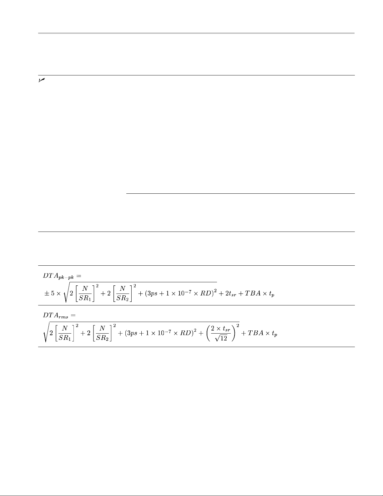
Table 2: Time base system specifications (cont.)
Characteristic Description
Delta-time m
accuracy
easurement
The formula to calculate the delta-time measurement accuracy (DTA) for a given instrument
setting and input signal is given in the following table. (See Table 3.) The formula assumes
insignificant signal content above Nyquist and insignificant error due to aliasing. The
abbreviations used in the formula are as follows:
SR
= slew rate around 1st point in measurement (1stedge)
1
= slew rate around 2nd point in measurement (2ndedge)
SR
2
N =input-referred noise (V
specifications.)
TBA = time base accuracy (5 ppm) (Refer to Long-term Sample Rate and Delay Time Accuracy
specifications.)
= delta-time measurement duration (sec)
t
p
RD = (record length)/(sample rate)
= 1/(sample rate)
t
sr
assume edge shape that results from Gaussian filter response
The term under the squareroot sign is the stability and is due to TIE (Time Interval Error). The
errors due to this term occur throughout a single-shot measurement. The second term is due
to both the absolute center-frequency accuracy and the center-frequency stability of the time
base and varies between multiple single-shot measurements over the observation interval (the
amount of time from the first single-shot measurement to the fi nal single-shot measurement).
)(RefertoRandom Noise and Sample Acquisition Mode
RMS
Specifications
3: Delta-Time measurement accuracy formula
Table
The terms used in these formulas are defined under Delta-time measurement accuracy, in the preceding table. (See Table 2.)
MDO4000 Series Specifications and Performance Ve rification 9
Page 18

Specifications
Triggering Sy
stem Specifications
The following table shows the trigger specifications for a nalog and digital
channels on the MDO4000 Series oscilloscopes. These specifications do not
applytotheR
NOTE. For RF, please see the analog to RF trigger skew specification. (See
page 17, RF Input Specifications.)
Table 4: Trigger specifications
Characteristic Description
Trigger bandwidth, Edge, typical
Trigger bandwidth, Pulse and Logic,
typical
Edge-type trigger sensitivity, DC
coupled, typical
Trigger jitter, typical
MDO4104-X 1 GHz
MDO4054-X
MDO4034-3
MDO4014-3
MDO4104-X 1 GHz
MDO4054-X
MDO4034-3
MDO4014-3
Model Trigger
MDO4104-X
MDO4054-X, MDO4034-3,
MDO4014-3
All models A ny input
All models Line Fixed
10 ps
RMS
100 ps
RMS
F input channel.
500 MHz
350 MHz
100 MHz
500 MHz
350 MHz
100 MHz
Source
Any input
channel
Any input
channel
channel
for edge-type trigger
for non edge-type trigger modes
Sensitivity
50 path:
0.40 div from DC to 50 MHz, increasing to
1 div at oscilloscope bandwidth
50 path:
1 mV/div to 4.98 mV/div — 0.75 div from
DC to 50 MHz, increasing to 1.3 div at
oscilloscope bandwidth.
5 mV/div — 0.40 div from DC to
50 MHz, increasing to 1 div at oscilloscope
bandwidth.
1M path:
1 mV/div to 4.98 mV/div – 0.75 div from
DC to 50 MHz, increasing to 1.3 div at
oscilloscope bandwidth.
5 mV/div – 0.40 div from DC to 50 MHz,
increasing to 1 div at oscilloscope
bandwidth.
10 MDO4000 Series Specifications and Performance Verification
Page 19

Table 4: Trigger specifications (cont.)
Characteristic Description
Edge-type trigger sensitivity, not DC
coupled, typical
Video-type trigger formats and field
rates
Video-type trigger sensitivity, typical
Lowest frequency for successful
operation of "Set Level to 50%"
function, typical
Logic-type or logic qualified trigger
or events-delay sensitivities, DC
coupled, typical
Pulse-type runt trigger sensitivities,
typical
Pulse-type trigger width and glitch
sensitivities, typical
Logic-type triggering, minimum logic
or rearm time, typical
Minimum clock pulse widths for
setup/hold time violation trigger,
typical
Trigger Coupling Typical Sensitivity
AC Coupling 1 div for frequencies above 45 Hz.
NOISE REJ 2.5 times the DC-coupled limits
HF REJ
LF REJ
Triggers from negative sync composite video, field 1, or field 2 for interlaced systems, on any
field, specific line, or any line for interlaced or noninterlaced systems. Supported systems
include NTSC, PAL, and SECAM.
Delayed and main trigger
Source Sensitivity
Any input channel
45 Hz
1.0 division from D C to maximum bandwidth
1.0 division from D C to maximum bandwidth
1.0 division
For all vertical settings, the minimums are:
Trigger type Pulse width Re-arm time Time between channels
Logic Not applicable 2 ns 1 ns
Time Qualified Logic
For logic, the time between channels refers to the length of time a logic state derived from
more than one channel must exist to be recognized. For events, the time is the minimum time
between a main and delayed event that will be recognized if more than one channel is used.
For all vertical settings, the minimums are:
Clock active Clock inactive
User hold time + 2.5 ns 2 ns
An active pulse width is the width of the clock pulse from its active edge (as defined in the
Clock Edge lower-bezel menu item) to its inactive edge. An inactive pulse width is the width
of the pulse from its inactive edge to its active edge.
The user hold time is the number selected by the user.
Specifications
Attenuates signals below 45 Hz.
1.0 times the DC-coupled limits from DC to 50 kHz.
Attenuates signals above 50 kHz
1.5 times the DC-coupled limits for frequencies above
50 kHz. Attenuates signals below 50 kHz
0.6 to 2.5 divisions of video sync tip
4ns 2ns 1ns
MDO4000 Series Specifications and Performance Ve rification 11
Page 20

Specifications
Table 4: Trigger specifications (cont.)
Setup/hold violation trigger, setup
and hold time ranges
Pulse type trigger, minimum pulse,
rearm time, transition time
Transition time trigger, delta time
range
Time range for glitch, pulse width,
timeout, time-qualified runt, or
time-qualified window triggering
Time Accuracy for Pulse, Glitch,
Timeout, or Width Triggering
B trigger after events, minimum
pulse width and maximum event
frequency, typical
B trigger, minimum time between
arm and trigger, typical
B trigger after time, time range
B trigger after events, event range
Feature Min Max
Setup time
Hold time 1 ns 1.0 ms
Setup + Hold time
Input coupling on clock and data channels must be the same.
For Setup time, positive numbers mean a data transition before the clock.
For Hold time, positive numbers mean a data transition after the clock edge.
Setup + Hold time is the algebraic sum of the Setup Time and Hold Time that you
programmed.
Pulse class Minimum
Glitch
Runt 4 ns 2 ns
Time-qualified runt
Width 4 ns
Slew rate (transition time)
For the trigger class width and the trigger class runt, the pulse width refers to the width of the
pulse being measured. The rearm time refers to the time between pulses.
For the trigger class slew rate, the pulse width refers to the delta time being measured. The
rearm time refers to the time it takes the signal to cross the two trigger thresholds again.
4nsto8s
4nsto8s
Time Range Accuracy
1 ns to 500 ns
520 ns to 1 s
4 ns, 500 MHz
4ns
For trigger after time, this is the time between the end of the time period and the B trigger
event.
For trigger after events, this is the time between the last A trigger event and the first B trigger
event.
4nsto8seconds
1 to 4,000,000
–0.5 ns 1.0 ms
0.5 ns 2.0 ms
Minimum rearm time
pulse width
4ns
4ns
4ns
±(20% of setting + 0.5 ns)
±(0.01% of setting + 100 ns)
2 ns + 5% of glitch width setting
8.5 ns + 5% of width s etting
2 ns + 5% of width upper limit setting
8.5 ns + 5% of delta time setting
12 MDO4000 Series Specifications and Performance Verification
Page 21

Table 4: Trigger specifications (cont.)
Specifications
Trigger level ranges
Trigger level accuracy, DC coupled,
typical
Trigger holdoff range
Maximum serial trigger bits 128 bits
Standard serial bus interface triggering
I2C Address Triggering: 7 and 10 bit user specified addresses, as well as General Call, START
SPI Data Trigger: 1 to 16 bytes of user-specified data
CAN Data Trigger: 1 to 8 bytes of user-specified data, including qualifiers of equal to (=), not equal
LIN
Source
Any input channel
Line Not applicable
Line trigger level is fixed at about 50% of the line voltage.
This specification applies to logic and pulse thresholds.
For signals having rise and fall times 10 ns.
Source
Any input channel ±0.20 div
Line Not applicable
20 ns minimum to 8 s maximum
byte, HS-mode, EEPROM, and CBUS
Data Trigger: 1 to 5 bytes of user specified data
Trigger On: Start, Repeated Start, Stop, Missing Ack, Address, Data, or Address and Data
Maximum Data R ate: 10 Mbps
Trigger On: SS Active, MOSI, MISO, or MOSI & MISO
Maximum Data R ate: 50 Mbps
to (<>), less than (<), greater than (>), less than or equal to (<=), greater than or equal to (>=)
Trigger On: Start of Frame, Type of Frame, Identifier, Data, Identifier and Data, End of
Frame, Missing Ack, or Bit Stuffing Errors
Frame Type: Data, Remote, Error, Overload
Identifier: Standard (11 bit) and Extended (29 bit) identifiers
Maximum Data R ate: 1 Mbps
Identifier Trigger: 6 bits of user-specified data, equal to (=)
Data Trigger: 1 to 8 bytes of user-specified data, including qualifiers of equal to (=), not
equal to (<>), less than (<), greater than (>), less than or equal to (<=), greater than or
equal to (>=), inside range, or outside range
Error: Sync, Identifier Parity, Checksum
Trigger On: Sync, Identifier, Data, Identifier & Data, Wakeup Frame, Sleep Frame, or Error
Maximum Data Rate: 100 kbps
Range
±8 divisions from center of screen
±8 divisions from 0 V when vertical LF reject
trigger coupling is selected
Range
MDO4000 Series Specifications and Performance Ve rification 13
Page 22

Specifications
Table 4: Trigger specifications (cont.)
FlexRay
Audio
I2S Data Trigger: 32 bits of user-specified data in a left word, right word, or either, including
Left Justified Data Trigger: 32 bits of user-specified data in a left word, right word, or either, including
Right Justified Data Trigger: 32 bits of user-specified data in a left word, right word, or either, including
TDM
RS-232
Indicator bits: Normal Frame, Payload Frame, Null Frame, Sync Frame, Startup Frame
Identifier Trigger: 11 bits of user-specified data, equal to (=), not equal to (<>), less than (<),
greater than (>), less than or equal to (<=), greater than or equal to (>=), Inside Range, or
Outside Range
Cycle Count Trigger: 6 bits of user-specified data, equal to (=)
Header Fields Trigger: 4 0 bits of user-specified data comprising Indicator Bits, Identifier,
Payload Length, Header CRC, Cycle Count, or equal to (=)
Data Trigger: 1 to 16 Bytes of user-specified data, with 0 to 253, or "don't care" bytes of data
offset, including qualifiers of equal to (=), not equal to <>, less than (<), greater than (>), less
than or equal to (<=), greater than or equal to (>=), Inside Range, Outside Range
End Of Frame: User-chosen types Static, Dynamic (DTS), and All
Error: Header CRC, Trailer CRC, Null Frame-static, Null Frame-dynamic, Sync Frame,
Startup Frame
Trigger On: Start of Frame, Indicator Bits, Identifier, Cycle Count, Header Fields, Data,
Identifier & Data, End of Frame, or Error
Maximum Data Rate: 100 Mbps
qualifiers of equal to (=), not equal to <>, less than (<), greater than (>), less than or equal to
(<=), greater than or equal to (>=), inside range, outside range
Trigger on: Word Select, Data
Maximum Data Rate: 12.5 Mbps
qualifiers of equal to (=), not equal to <>, less than (<), greater than (>), less than or equal to
(<=), greater than or equal to (>=), inside range, outside range
Trigger on: Word Select, Data
Maximum Data Rate: 12.5 Mbps
qualifiers of equal to (=), not equal to <>, less than (<), greater than (>), less than or equal to
(<=), greater than or equal to (>=), inside range, outside range
Trigger on: Word Select, Data
Maximum Data Rate: 12.5 Mbps
Data Trigger: 32 bits of user-specifi ed data in a channel 0-7, including qualifiers of equal to
(=), not equal to <>, less than (<), greater than (>), less than or equal to (<=), greater than or
equal to (>=), inside range, outside range
Trigger on: Frame Sync, Data
Maximum Data Rate: 25 Mbps
Bit Rate: 50 bps to 10 Mbps
Data Bits: 7, 8, or 9
Parity: None, Odd, or Even
Trigger on: Tx Start bit, Rx Start bit, Tx End of Packet, Rx End of Packet, Tx Data, Rx
Data, Tx Parity Error, Rx Parity Error
End of Packet: 00(NUL),OA(LF),OD(CR),20(SP),FF
14 MDO4000 Series Specifications and Performance Verification
Page 23

Table 4: Trigger specifications (cont.)
MIL-STD-1553 Bit Rate: 1Mb/s
Trigger on: Sync, Word Type (Command, Status, Data), Command Word (set RT Address
(=, ,<,>,, , inside range, outside range), T/R, Sub-address/Mode, Data Word
Count/Mode Code, and Parity individually), Status Word (set RT Address ((=, ,<,>,,
, inside range, outside range), M essage Error, Instrumentation, Service Request Bit,
Broadcast Command Received, Busy, Subsystem Flag, Dynamic Bus Control Acceptance
(DBCA), Terminal Flag, and Parity individually) Data Word (user-specified 16-bit data value)
Error (Sync, Parity, Manchester, Non-contiguous data) Idle Time (minimum time selectable
from 4 s to 100 s; maximum time selectable from 12 s to 100 s; trigger on < minimum,
> maximum, inside range, outside range)
USB Data Rates Supported: HS: 480 Mbps, Full: 12 Mbps, Low: 1.5 Mbps
Trigger On: Sync, R eset, Suspend, Resume, End of Packet, Token (Address) Packet, Data
Packet, Handshake Packet, Special Packet, Error
NOTE. HIGH SPEED support available only on MDO4104-3 and MDO4104-6 models.
Ethernet
Bit Rate: 10BASE-T, 10 Mbps; 100BASE-TX, 100 Mbps
Trigger On: Start Frame Delimiter (SFD), MAC Address, MAC Length/Type, IP Header, TCP
Header, TCP/IPv4/MAC Client Data, End of Packet, Idle, FCS (CRC) Error, MAC Q-Tag
control Information.
Specifications
Digital Acquisition System Specifications
The following table shows the digital acquisition specifications for the MDO4000
Series oscilloscopes.
Table 5: Digital acquisition specifications
Characteristic Description
Threshold voltage range –40 V to +40 V
Digital channel timing resolution
Logic threshold accuracy
Minimum detectable pulse width,
typical
2 ns main memory, 60.6 ps for MagniVu memory
±(100 mV + 3% of threshold setting after calibration)
Requires v alid SPC, as described in step 2 of the Self Test. (See page 62, Self Test.)
1ns
Using M agniVu memory. Requires the use of 342-1140-00 ground clip on each channel.
MDO4000 Series Specifications and Performance Ve rification 15
Page 24

Specifications
P6616 Digital
Probe Input Specifications
The following table shows the P6616 Digital Probe specifications.
Table 6: P6616 digital probe input specifications
Characteristic Description
Number of channels
Input resistance, typical
Input capacitance, typical 3.0 pF
Minimum input signal swing, typical 400 mV
Maximum input signal swing, typical
Maximum Input Toggle Rate, typical 500 MHz
Absolute maximum input voltage, typical
Channel-to-channel skew, typical
16 digital inputs
100 k to ground
Measured at the podlet input. Requires the use of 342-1140-00 ground clip on each
channel
p-p
Requires the use of 342-1140-00 ground clip on each channel
30 V
for fin 200 MHz (centered around the DC threshold voltage) at the P6616
p-p
probe tip.
10 V
for fin>200 MHz (centered around the DC threshold voltage) at the P6616
p-p
probe tip.
Failure to meet this input signal requirement will compromise the AC performance of the
digital channel. It might also damage the input circuitry. See the Absolute maximum
input voltage specification.
Maximum frequency sine wave input (at the minimum signal swing amplitude) that can
accurately be reproduced as a logic square wave.
Requires the use of a 342-1140-00 ground clip on each channel.
Higher toggle rates can be achieved with higher amplitudes.
±42 V peak at the P6616 input (not at the instrument input)
Probe input voltages beyond this limit could permanently damage the instrument and
the P6616 probe.
200 ps
Digital channel to digital channel only.
This is the propagation path skew and ignores skew contributions due to threshold
inaccuracies (see Threshold accuracy) and sample binning (see Digital channel timing
resolution). Factory calibration/deskew is required to achieve this number.
16 MDO4000 Series Specifications and Performance Verification
Page 25

Specifications
RF Input Speci
fications
The following table shows the RF input specifications for the MDO4000 Series
oscilloscopes.
Table 7: RF i
Characteristic Description
Frequency measurement resolution 1 Hz
Span Span adjustable in 1-2-5 sequence
Resolution bandwidth (RBW) Adjustable in 1-2-3-5 sequence. Maximum of 10 MHz RBW
Input vertical range Vertical measurement range +30 dBm to DANL.
l display range
Leve
ference level
Re
rtical position
Ve
aximum operating input level
M
nput specifications
MDO4104-6, MDO4054-6 50 kHz to 6 GHzCenter frequency range
MDO4104-3, MDO4054-3,
MDO4034-3, MDO4014-3
Variable resolution = 1% of the next span setting
The MDO4
The MDO4XX4-3 Span is adjustable from 1 kHz to 3 GHz
Minimum RBW for Windowing functions as follows:
60 dB/
Vert
Attenuator settings from 0 to 45 dB, in 5 dB steps
Log s
Measurement points: 1000
Marker level readout resolution: Log scale: 0.1 dB
Max
Trace functions: maximum hold, average, minimum hold, normal, spectrogram slice
(uses normal trace)
Det
tting range: –140 dB m to +30 dBm, in steps of 5 dBm
Se
Default setting: 0 dBm
–10 divisions to +10 divisions (displayed in dB)
Average continuous p ower: +30 dBm (1W)
DC maximum before damage: ±40 Vdc
Maximum “no damage” 33 dBm (2W) CW
Peak pulse power: +45 dBm (32W)
Peak Pulse Power is defined as: <10 us pulse width, <1% duty cycle, and a reference
level of +10 dBm.
XX4-6 Span is adjustable from 1 kHz to 6 GHz
30 Hz Ka
20 Hz Rectangular, Hamming, Hanning
50 Hz Flat-Top
ical setting of 1 dB/div to 20 dB/div in a 1-2-5 sequence
imum number of RF traces: 4
ection methods: Positive-Peak, negative-peak, sample, average
iser, Blackman-Harris
3 dB shape factor (Kaiser, Blackman-Harris) 4:1 ratio
cale and units: dBm, dBmV, dBµV, dBµW, dBmA, dBµA
50kHzto3GHz
MDO4000 Series Specifications and Performance Ve rification 17
Page 26

Specifications
Table 7: RF input specifications (cont.)
Characteristic Description
Frequency measurement accuracy Marker Frequency
All models: ±(Reference Frequency Error * MarkerFrequency + .001 * span + 2) Hz.
Marker Frequency with Span/RBW 1000:1
Reference frequency error = ±5 ppm
Phase noise
Residual FM, typical 100 Hz peak-to-peak in 100 ms
Displayed average noise level
)
(DANL
Level measurement uncertainty
10 kHz offset: < –90 dBc/Hz (< –95 dBc/Hz, typical)
100 kHz offset: < –95 dBc/Hz (< –98 dBc/Hz, typical)
1 MHz offset: < –113 dBc/Hz (< –118 dBc/Hz, typical)
Max RBW % Error = (0.5/(25 x WF)) * 100Resolution bandwidth (RBW) accuracy
WF =
Rectangular: 0.89
Hamming: 1.30
Hanning: 1.44
Blackman-Harris: 1.90
Kaiser: 2.23
Flat-Top: 3.77
MDO4104-6
MDO4054-6
MDO4104-3, MDO4054-3,
MDO4034-3, MDO4014-3
>5 dBm1 dB gain compression
With reference level set to –10 dBm
< ± 1 dB (<±0.5 dB typical) 20 °C to 3 0 °C temperature range, reference level 10 dBm to
–25 dBm. Input level ranging from reference level to 30 dB below reference level.
< ± 1.5 dB , Ta > 30 °C and Ta < 20 °C temperature range, reference level 10 dBm to –25
dBm. Input level ranging from reference level to 30 dB below reference level.
50kHzto5MHz:
< –130 dBm/Hz ( < –134 dBm/Hz, typical)
5MHzto3GHz:
< –148 dBm/Hz (< –152 dBm/Hz, typical)
3GHzto6GHz:
< –140 dBm/Hz (< –143 dBm/Hz, typical)
50kHzto5MHz:
< –130 dBm/Hz (< –134 dBm/Hz, typical)
5MHzto3GHz:
< –148 dBm/Hz (< –152 dBm/Hz, typical)
18 MDO4000 Series Specifications and Performance Verification
Page 27

Table 7: RF input specifications (cont.)
Characteristic Description
Spurious response
Third order intermodulation
distortion
Image and IF rejection
dual spurious response
Resi
Power level trigger frequency and
amplitude range
RF to analog channel skew, typical Maximum time between analog channels triggered and RF channel:
Power level trigger limits
Crosstalk to RF channel from
analog channels
Channel power accuracy, Typical < ±1 dB (<±0.5 dB Typical) 20-30 °C temperature range
Occupied bandwidth accuracy, Typical ± Span/1000
Adjacent channel power ratio, Typical -58 dBc
2nd and 3rd harmonic distortion >100 MHz: < –55 dBc (< –60 dBc Typical)
With auto settings on, signals –5 dB below reference level
2nd and 3rd harmonic distortion: >50 kHz: < –55 dBc (< –60 dBc Typical)
With auto settings on, signals –5 dB below reference level, and reference level -15 dBm
2nd order intermodulation distortion: >200 MHz: < –55 dBc (< –60 dBc Typical)
With auto settings on and signals –5 dB below reference level
2nd order intermodulation distortion: >50 kHz: < –55 dBc (< –60 dBc Typical)
With auto settings on, signals –5 dB below reference level, and reference level –15 dBm
Other A/D spurs: < –55 dBc (< –60 dBc Typical)
3rd o rder intermodulation distortion >15 MHz: < –60 dBc (< –63 dBc Typical)
With auto settings on, signals –5 dB below reference level
3rd o rder intermodulation distortion >50 kHz: < –60 dBc (< –63 dBc Typical)
With auto settings on, signals –5 dB below reference level, and reference level –15 dBm
< –50 dBc (< –55 dBc typical)
With –10 dBm reference level
< –78 dBm
With –25 dBm reference level and RF input terminated with 50 .
Frequency range:
1 MHz to 6 GHz (MDO4XX4-6 models)
1 MHz to 3 GHz (MDO4XX4-3 models)
Amplitude range: 30 dBm to -40 dBm
<5ns
Center frequency 1 MHz to 3.25 GHz: –35 dB from reference level
Center frequency >3.25 GHz: –13 dB from reference level
Minimum pulse duration: 10 s ON time with a minimum settling OFF time of 10 s.
< -68 dB from reference level (1 GHz oscilloscope input frequencies)
< -48 dB from reference level (>1 GHz to 2 GHz oscilloscope input frequencies)
Full scale amplitude with 50 input and 100 mV/div vertical setting with direct input (no
probes).
< ±1.5 dB, Ta >30 °C and Ta <20 °C temperature range
Specifications
MDO4000 Series Specifications and Performance Ve rification 19
Page 28

Specifications
Display Syste
mSpecifications
The following table shows the display specifications for the MDO4000 Series
oscilloscopes.
Table 8: Dis
Characteristic Description
Display typ
Display resolution
Luminance, typical
Waveform display color scale The TFT display can support up to 262,144 colors. A subset of these colors is used for the
play system specifications
e
Display area: 210.4 mm (8.28 in) (H) x 157.8 mm (6.21 in) (V), 264 mm (10.4 in) diagonal,
6-bit RGB full color, XGA (1024 x 768) TFT liquid crystal display (LCD).
1024 X 768 XGA display resolution
400 cd/m
oscillo
2
scope display. The colors that are used are fixed and not changeable by the user.
20 MDO4000 Series Specifications and Performance Verification
Page 29

Specifications
Interfaces an
d Input/Output Port Specifications
The following table shows the interfaces and input/output port specifications
for the MDO4000 Series oscilloscopes.
Table 9: Int
Characteristic Description
Ethernet interface Standard on all models: 10/100/1000 Mbps
GPIB interface Available as an optional accessory (TEK-USB-488 GPIB to USB Adapter), which connects
Video signal output
USB inte
Probe compensator output voltage
and frequency, typical
Auxiliary output (AUX O UT)
Trigger O ut or
Reference Clock Out
External Reference nominal input
requency
f
External Reference input frequency
ariation tolerance, typical
v
External Reference input sensitivity,
typical
External Reference input maximum
input signal
External Reference input impedance,
typical
erfaces and Input/Output port specifications
to the USB Device and USB Host port.
ol interface is incorporated into the instrument user interface.
-sub VGA connector.
t connectors (2.0 HS), two on the instrument front and two on the rear.
t: 0 – 2.5 V amplitude, ± 2% (Source Impedance of 1k)
± 25%
n s et the Auxiliary output to Trigger Out or Reference Clock Out.
ore than 0.2% (2000 ppm) different than the nominal reference frequency or reference
for input frequencies between 9.9 MHz and 10.1 MHz
p-p
p-p
rface
The contr
A 15-pin D
4USBhos
1 USB device connector (2.0 HS), on the instrument rear panel.
All are standard on all models.
Output Voltage
Defaul
TPPXX00 Cal Mode: 0 – 2.5 V amplitude, ± 5% (Source Impedance of 25)
Frequency
1kHz,
You ca
Reference Clock Out: Outputs the 10 MHz oscilloscope reference clock.
Trigger Out: A H IGH to LOW transition i ndicates that the trigger occurred.
Trigger output logic levels
Characteristic
Vout (HI)
Vout (LO) 0.7 V into a load of 4mA
10 MHz
You must select either the internal reference (default) or 10 MHz external.
9.9 MHz to 10.1 MHz
You must run SPC, described in step 2 of the Self Test, whenever the external reference is
m
at which SPC was last run. (See page 62, Self Test.) The time base changes in
correspondence to the fluctuations in the external reference.
1.5 V
7V
Rin = 1.5 k ±20% in parallel with 15 pF ±5 pF at 10 MHz
its
Lim
5 V open circuit
2.
1.0Vintoa50 load to ground
0.25 V into a 50 load to ground
MDO4000 Series Specifications and Performance Ve rification 21
Page 30

Specifications
Data Handling
Specifications
The following table shows the data handling specifications for the MDO4000
Series oscilloscopes.
Table 10: Da
Characteristic Description
Nonvolatil
typical
Real-time clock A programmable clock providing time in years, months, days, hours, minutes, and seconds
ta handling specifications
e memory retention time,
No time limit for front-panel settings, saved waveforms, setups, or calibration constants.
10 M and 20 M records saved as Reference waveforms are not saved i n the nonvolatile
memory and
they will not be saved across a power cycle.
Power Supply System Specifications
The foll
MDO4000 Series oscilloscopes.
Table 11: Power supply system specifications
Characteristic Description
Operating line frequency and voltage
range
Maximum power consumption: 225 W
Source voltage 100 V to 240 V ±10%
Source frequency (85 to 264 V) 45 Hz to 66 Hz
Fuse rating
owing table shows the power supply system specifications for the
Volts: 100 – 240; Hz: 50 – 60
Volts: 115: Hz: 400
(100 V to 132 V) 360 Hz to 440 Hz
T6.3AH, 250 VAC
fuse cannot be replaced by the user.
The
22 MDO4000 Series Specifications and Performance Verification
Page 31

Specifications
Environmenta
lSpecifications
The following table shows the environmental specifications for the MDO4000
Series oscilloscopes.
Table 12: En
Characteristic Description
Temperatur
Humidity
e
Altitud
Pollution Degree Pollution Degree 2, indoor use only
vironmental specifications
e
Operating: 0 ° C to +50 °C (32 °F to +122 °F)
Nonoperating: -20 °C to +60 °C (-4 °F to +140 °F)
Operating:
High: 40 °
Low: 0 °C to 40 °C (32 °F to 104 °F), 10% to 90% relative humidity
Nonoperating:
High: 40 °
Low: 0 °C to 40 °C (32 ° F to 104 °F), 5% to 90% relative humidity
Operating: 3,000 m (9,843 ft)
Nonoperating: 12,000 m (39,370 ft)
C to 50 °C (104 °F to 122 °F), 10% to 60% relative humidity
C to 60 °C (104 °F to 140 °F), 5% to 60% relative humidity
MDO4000 Series Specifications and Performance Ve rification 23
Page 32

Specifications
Mechanical Sp
ecifications
The following table shows the mechanical specifications for the MDO4000 Series
oscilloscopes.
Table 13: Me
Characteristic Description
Weight
Dimensions
arance Requirements
Cle
chanical specifications
Benchtop configuration (oscilloscope only)
Requirements that follow are nominal:
11. 0 lbs (5
18.8 lbs (8.5 kg), instrument with rackmount, without front cover
23.6 lbs (10.7 kg), when packaged for domestic shipment (without rackmount)
Benchtop
Requirements that follow are nominal and unboxed
Height:
29 mm) feet folded in, handle folded down
9.0in(2
9.8 in (249 mm) feet folded out, handle folded down
11.5 in (292 mm) feet folded in, handle folded up
(312 mm) feet folded out, handled folded up
12.3 in
Width:
17.3 in (439 mm) from handle hub to handle hub
Depth:
5.8 in (147 mm) from back of feet to front of knobs
6.1 in (155 mm) from back of feet to front of front cover
(249 mm) from handle to front of knobs (handle folded to back side of unit)
9.8 in
Box Dimensions:
Height: 15.7 in (399 mm)
: 15.6 in (396 mm)
Width
Length: 22.2 in (564 mm)
Rackmount configuration
irements that follow are nominal and unboxed (5U rack sizes):
Requ
Height: 8.6 in ( 218 mm)
Width: 19.2 in (488 mm), from outside of handle to outside of handle
th: 15.1 in (384 mm), from outside of handle to back of slide
Dep
(0 in), top
0mm
0 in (0 mm), bottom, on feet, with flip stands down
2 in (50.8 mm), left side (facing the front of the instrument)
n (0 mm), right side (facing the front of the instrument)
0i
2 in (50.8 mm), rear (where the power cord is plugged in)
.0 kg), stand-alone instrument, without front cover.
configuration (oscilloscope only)
24 MDO4000 Series Specifications and Performance Verification
Page 33

Specifications
TPA-N-PRE Spe
cifications
The following tables shows the TPA-N-PRE Preamplifier specifications.
Table 14: TPA-N-PRE specifications
Characteristic Description
Frequency range
Preamp gain
Displayed average noise level
(DANL) of the MDO4000 with the
preamp attached to the MDO’s RF
input
Level measurement uncertainty of the
MDO4000 with the preamp attached
to the MDO’s RF input
Maximum operating input level of the
MDO4000 with the preamp attached
to the MDO’s RF input
Reference level range of the
MDO4000 with the preamp attached
to the MDO’s RF input
Connector type SMA – female (outside threads)
Temperature
Humidity
Preamp: 9 kHz to 6 GHz
MDO4XX4-6 with preamp: 50 kHz to 6 GHz
MDO4XX4-3 with preamp: 50 kHz to 3 GHz
Amplifying state: 12 dB (nominal)
Bypass state: –1.5 dB (nominal)
With the preamp mode set to “Auto” and the reference level set to -40 dBm
MDO4XX4-6:
50 kHz to 5 MHz: < –140 dBm/Hz (–144 dBm/Hz typical)
5 MHz to 3 GHz: < –158 dBm/Hz (–162 dBm/Hz typical)
3 GHz to 6 GHz: < –150 dBm/Hz (–153 dBm/Hz typical)
MDO4XX4-3:
50 kHz to 5 MHz: < –140 dBm/Hz (–144 dBm/Hz typical)
5 MHz to 3 GHz: < –158 dBm/Hz (–162 dBm//Hz typical)
With the preamp mode set to “Auto”, reference level 10 dBm to –40 dBm and input level
ranging from reference level to 30 dB below reference level. Specifications exclude
mismatch error at the preamp input and applies to both amplifying and bypass states.
< ±1.5 dB (typical), 20 ° C to 30 °C temperature range.
±2.3 dB (typical), over full operating range.
Average continuous power: +30 dBm (1 W)
DC maximum before damage: ±20 V DC
Maximum power before damage (CW): +30 dBm (1 W)
Maximum power before damage (pulse): +45 dBm (32 W)
(<10 s pulse width, <1% duty cycle, and reference level of +10 dBm)
Amplifying state: –30 dBm to DANL
Bypass state: +30 dBm to D ANL
Operating: 0 °C to +50 °C
Non-operating: –20 °C to +60 °C
Operating:
High: 40 °C to 50 °C (104 °F to 122 °F), 10% to 60% RH
Low: 0 °C to 40 °C (32 °F to 104 °F), 5% to 90% RH
Non-operating:
High: 40 °C to 50 °C (104 °F to 122 °F), 10% to 60% RH
Low: 0 °C to 40 °C (32 °F to 104 °F), 5% to 90% RH
MDO4000 Series Specifications and Performance Ve rification 25
Page 34

Specifications
Characteristic Description
Altitude
Power requirements
Regulatory
Recommended oscilloscopes
Operating: Up to 3,000 meters
Non-operating: Up to 12,000 meters
The TPA-N-PRE is powered directly from the RF input on the M DO 4000 Series oscilloscope
Compliance labeling: WEEE (European Union)
MDO4000 Mixed Domain Oscilloscopes
NOTE. For b
firmware from www.tektronix.com
est probe support, download and install the latest version of the oscilloscope
26 MDO4000 Series Specifications and Performance Verification
Page 35

Performance Verification
The performance verification procedures verify the performance of your
instrument. They do not adjust your instrument. If your instrument fails any
of the perfor
factory adjustment performed. See the contact information on the back of the
title page of this manual.
This section contains performance verification procedures for the specifications
marked with the
Please ignore checks that do not apply to the specific model you are testing.
Print the test record on the following pages and use it to record the performance
test results for your oscilloscope.
NOTE. Completion of the performance verification procedure does not update the
stored time and date of the latest successful adjustment. The date and time are
update
mance verification tests, you should contact Tektronix to have the
d only when the instrument is adjusted by Tektronix.
symbol. These procedures cover all MDO4000 Series models.
MDO4000 Series Specifications and Performance Ve rification 27
Page 36

Performance Ve rification
The following e
quipment, or a suitable equivalent, is required to complete these
procedures. You might need additional cables and adapters, depending on the
actual test equipment you use.
Table 15: Required equipment
Description Minimum requirements Examples
DC voltage source 3 m V to 4 V, ±0.1% accuracy
Leveled sine wave generator
Time mark generator 80 ms period, ±1 ppm accuracy, rise time
Signal generator Frequency: to at least 6 GHz
Hybrid coupler (power combiner) Connects the output of two generators to
Logic probe Low capacitance digital probe, 16
BNC-to-0.1 inch pin adapter to connect
the logic probe to the signal source.
Digital multimeter (DMM) 0.1% accuracy or better Fluke 177 Series Digital Multimeter
Power meter
Power head
Power splitter
Male N-N adapter For connecting between the power splitter
One 50 terminator Impedance 50 ; connectors: female
One 50 terminator Impedance 50 ; Male N connector
One 50 BNC coaxial cable
One 50 SMA coaxial cable N connector to SMA
Three SMA cables With the correct connector to fit your
50 kHz to 1000 MHz, ±4% amplitude
accuracy
<50ns
Frequency accuracy: 5 ppm
the oscilloscope RF input
channels.
BNC-to-0.1 inch pin adapter; female BNC
to 2x16. 01 inch pin headers.
Frequency range at least 50 kHz – 6 GHz Agilent E9304A Average Power Sensor
BNC input, male BNC output
Male-to-male connectors Tektronix part number 012-0057-01
generator output.
Fluke 9500B Oscilloscope Calibrator with
a 9510 Output Module
Anritsu MG3692B Options 2A, 3A, 4, 15A,
16, 22, SM5821
Rohde & Schwarz SMT06
(Two generators are needed for checking
Third Order Intermodulation Distortion)
Krytar 3005070
P6616 probe; standard accessory shipped
with MDO4000 Series oscilloscopes.
Tektronix adapter part number
679-6240-00; to connect the Fluke
9500B to the P6616 probe.
Agilent N1913A Single-Channel Power
Meter
Agilent 11667A Power Splitter
ad the oscilloscope RF Input
Tektronix part number 011-0049-02
For terminating the RF Input
Tektronix part number 174-6025-00 (6 ft)
Tektronix part number 174-6026-00 (2 ft)
28 MDO4000 Series Specifications and Performance Verification
Page 37

Performance Verification
Test Record
Model Serial Procedure performed by Date
Test Passed Failed
Self Test
Input Impedance
Performance checks Vertical scale Low limit Test result High limit
Channel 1 Input
Impedance, 1 M
Channel 1 Input
Impedance, 250 k
Impedance, 50
Channel 2 Input
Impedance, 1 M
Channel 2 Input
Impedance, 250 k
Impedance, 50
Channel 3 Input
Impedance, 1 M
Channel 3 Input
Impedance, 250 k
Impedance, 50
Channel 4 Input
Impedance, 1 M
Channel 4 Input
Impedance, 250 k
Impedance, 50
10 mV/div 990 k 1.01 M
100 mV/div 990 k 1.01 M
1 V/div 990 k 1.01 M
100 mV/div 245 k 255 k
10 mV/div 49.5 50.5 Channel 1 Input
100 mV/div 49.5 50.5
10 mV/div 990 k 1.01 M
100 mV/div 990 k 1.01 M
1 V/div 990 k 1.01 M
100 mV/div 245 k 255 k
10 mV/div 49.5 50.5 Channel 2 Input
100 mV/div 49.5 50.5
10 mV/div 990 k 1.01 M
100 mV/div 990 k 1.01 M
1 V/div 990 k 1.01 M
100 mV/div 245 k 255 k
10 mV/div 49.5 50.5 Channel 3 Input
100 mV/div 49.5 50.5
10 mV/div 990 k 1.01 M
100 mV/div 990 k 1.01 M
1 V/div 990 k 1.01 M
100 mV/div 245 k 255 k
10 mV/div 49.5 50.5 Channel 4, Input
100 mV/div 49.5 50.5
MDO4000 Series Specifications and Performance Ve rification 29
Page 38

Performance Ve rification
DC Balance
Performance checks Vertical scale Low limit Test result High limit
Channel 1 DC
Balance, 50 ,20MHz
BW
Channel 1 DC
Balance, 1 M,
zBW
20 MH
Channel 1 DC
Balance, 50 ,
250 MHz BW
Channel 1 DC
Balance, 1 M,
250 MHz BW
Channel 1 DC
Balance, 50 ,Full
BW
Channel 1 DC
Balance, 1 M,Full
BW
1 mV/div
2 mV/div
5 mV/div
10 mV/div
20 mV/div
49.8 mV/div
50 mV/div
100 mV/div
200 mV/div
500 mV/div
1V/div
1 mV/div
2 mV/div
5 mV/div
10 mV/div
20 mV/div
100 mV/div
500 mV/div
1V/div
10 V/div
20 mV/div
20 mV/div
20 mV/div
20 mV/div
-0.2 mV 0.2 mV
-0.2 mV 0.2 mV
-0.5 mV 0.5 mV
-1 mV 1 mV
-2 mV 2 mV
-4.98 mV 4.98 mV
-5 mV 5 mV
-10 mV 10 mV
-20 mV 20 mV
-50 mV 50 mV
V
-100 m
V
-0.2 m
mV
-0.4
-1 mV 1 mV
V
-2 m
mV
-4
0mV
-2
100 mV
-
200 mV
-
-2 V 2 V
-2 mV 2 mV
-4 mV 4 mV
-2 mV 2 mV
-4 mV 4 mV
100 mV
0.2 mV
0.4 m
2mV
V
4m
mV
20
00 mV
1
00 mV
2
V
30 MDO4000 Series Specifications and Performance Verification
Page 39

Performance Verification
DC Balance
Performance checks Vertical scale Low limit Test result High limit
Channel 2 DC
Balance, 50 ,20MHz
BW
Channel 2 DC
Balance, 1 M,
zBW
20 MH
Channel 2 DC
Balance, 50 ,
250 MHz BW
Channel 2 DC
Balance, 1 M,
250 MHz BW
Channel 2 DC
Balance, 50 ,Full
BW
Channel 2 DC
Balance, 1 M,Full
BW
1 mV/div
2 mV/div
5 mV/div
10 mV/div
20 mV/div
49.8 mV/div
50 mV/div
100 mV/div
200 mV/div
500 mV/div
1V/div
1 mV/div
2 mV/div
5 mV/div
10 mV/div
20 mV/div
100 mV/div
500 mV/div
1V/div
10 V/div
20 mV/div
20 mV/div
20 mV/div
20 mV/div
-0.2 mV 0.2 mV
-0.2 mV 0.2 mV
-0.5 mV 0.5 mV
-1 mV 1 mV
-2 mV 2 mV
-4.98 mV 4.98 mV
-5 mV 5 mV
-10mV 10mV
-20mV 20mV
-50mV 50mV
V
-100 m
V
-0.2 m
mV
-0.4
-1 mV 1 mV
V
-2 m
mV
-4
0mV
-2
100 mV
-
200 mV
-
-2 V 2 V
-2 mV 2 mV
-4 mV 4 mV
-2 mV 2 mV
-4 mV 4 mV
100 mV
0.2 mV
0.4 m
2mV
V
4m
mV
20
00 mV
1
00 mV
2
V
MDO4000 Series Specifications and Performance Ve rification 31
Page 40

Performance Ve rification
DC Balance
Performance checks Vertical scale Low limit Test result High limit
Channel 3 DC
Balance, 50 ,20MHz
BW
Channel 3 DC
Balance, 1 M,
zBW
20 MH
Channel 3 DC
Balance, 50 ,
250 MHz BW
Channel 3 DC
Balance, 1 M,
250 MHz BW
Channel 3 DC
Balance, 50 ,Full
BW
Channel 3 DC
Balance, 1 M,Full
BW
1 mV/div
2 mV/div
5 mV/div
10 mV/div
20 mV/div
49.8 mV/div
50 mV/div
100 mV/div
200 mV/div
500 mV/div
1V/div
1 mV/div
2 mV/div
5 mV/div
10 mV/div
20 mV/div
500 mV/div
100 mV/div
1V/div
10 V/div
20 mV/div
20 mV/div
20 mV/div
20 mV/div
-0.2 mV 0.2 mV
-0.2 mV 0.2 mV
-0.5 mV 0.5 mV
-1 mV 1 mV
-2 mV 2 mV
-4.98 mV 4.98 mV
-5 mV 5 mV
-10 mV 10 mV
-20 mV 20 mV
-50 mV 50 mV
V
-100 m
V
-0.2 m
mV
-0.4
-1 mV 1 mV
V
-2 m
mV
-4
00 mV
-1
20 mV
-
200 mV
-
-2 V 2 V
-2 mV 2 mV
-4 mV 4 mV
-2 mV 2 mV
-4 mV 4 mV
100 mV
0.2 mV
0.4 m
2mV
V
4m
0mV
10
0mV
2
00 mV
2
V
32 MDO4000 Series Specifications and Performance Verification
Page 41

Performance Verification
DC Balance
Performance checks Vertical scale Low limit Test result High limit
Channel 4 DC
Balance, 50 ,20MHz
BW
Channel 4 DC
Balance, 1 M,
zBW
20 MH
Channel 4 DC
Balance, 50 ,
250 MHz BW
Channel 4 DC
Balance, 1 M,
250 MHz BW
Channel 4 DC
Balance, 50 ,Full
BW
Channel 4 DC
Balance, 1 M,Full
BW
1 mV/div
2 mV/div
5 mV/div
10 mV/div
20 mV/div
49.8 mV/div
50 mV/div
100 mV/div
200 mV/div
500 mV/div
1V/div
1 mV/div
2 mV/div
5 mV/div
10 mV/div
20 mV/div
500 mV/div
100 mV/div
1V/div
10 V/div
20 mV/div
20 mV/div
20 mV/div
20 mV/div
-0.2 mV 0.2 mV
-0.2 mV 0.2 mV
-0.5 mV 0.5 mV
-1 mV 1 mV
-2 mV 2 mV
-4.98 mV 4.98 mV
-5 mV 5 mV
-10mV 10mV
-20mV 20mV
-50mV 50mV
V
-100 m
V
-0.2 m
mV
-0.4
-1 mV 1 mV
V
-2 m
mV
-4
00 mV
-1
20 mV
-
200 mV
-
-2 V 2 V
-2 mV 2 mV
-4 mV 4 mV
-2 mV 2 mV
-4 mV 4 mV
100 mV
0.2 mV
0.4 m
2mV
V
4m
0mV
10
0mV
2
00 mV
2
V
MDO4000 Series Specifications and Performance Ve rification 33
Page 42

Performance Ve rification
DC Gain Accuracy
Performance checks Bandwidth Vertical scale Low limit Test result High limit
MDO4104-3, MDO4104-6
Channel 1
DC Gain Accuracy,
0 V offset, 0
position, 50
Channel 2
DC Gain Accuracy,
offset, 0 V vertical
0V
position, 50
Vvertical
20 MHz
Hz
250 M
Full
Hz
20 M
250 MHz
Full
1 mV/div -2.0% 2.0%
2 mV/div -1.5% 1.5%
5 mV/div -1.5% 1.5%
10 mV/div -1.5% 1.5%
20 mV/div -1.5% 1.5%
49.8 mV/div -3.0% 3.0%
50 mV/div -1.5% 1.5%
100 mV/div -1.5% 1.5%
200 mV/div -1.5% 1.5%
500 mV/div -1.5% 1.5%
1 V/div -1.5% 1.5%
20 mV/div -1.5% 1.5%
20 mV/div -1.5% 1.5%
1 mV/div -2.0% 2.0%
2 mV/div -1.5% 1.5%
5 mV/div -1.5% 1.5%
10 mV/div -1.5% 1.5%
20 mV/div -1.5% 1.5%
49.8 mV/div -3.0% 3.0%
50 mV/div -1.5% 1.5%
100 mV/div -1.5% 1.5%
200 mV/div -1.5% 1.5%
500 mV/div -1.5% 1.5%
1 V/div -1.5% 1.5%
20 mV/div -1.5% 1.5%
20 mV/div -1.5% 1.5%
34 MDO4000 Series Specifications and Performance Verification
Page 43

Performance Verification
DC Gain Accuracy
Performance checks Bandwidth Vertical scale Low limit Test result High limit
MDO4104-3, MDO4104-6
Channel 3
DC Gain Accuracy,
0 V offset, 0
position, 50
Channel 4
DC Gain Accuracy,
offset, 0 V vertical
0V
position, 50
Vvertical
20 MHz
Hz
250 M
Full
Hz
20 M
250 MHz
Full
1 mV/div -2.0% 2.0%
2 mV/div -1.5% 1.5%
5 mV/div -1.5% 1.5%
10 mV/div -1.5% 1.5%
20 mV/div -1.5% 1.5%
49.8 mV/div -3.0% 3.0%
50 mV/div -1.5% 1.5%
100 mV/div -1.5% 1.5%
200 mV/div -1.5% 1.5%
500 mV/div -1.5% 1.5%
1 V/div -1.5% 1.5%
20 mV/div -1.5% 1.5%
20 mV/div -1.5% 1.5%
1 mV/div -2.0% 2.0%
2 mV/div -1.5% 1.5%
5 mV/div -1.5% 1.5%
10 mV/div -1.5% 1.5%
20 mV/div -1.5% 1.5%
49.8 mV/div -3.0% 3.0%
50 mV/div -1.5% 1.5%
100 mV/div -1.5% 1.5%
200 mV/div -1.5% 1.5%
500 mV/div -1.5% 1.5%
1 V/div -1.5% 1.5%
20 mV/div -1.5% 1.5%
20 mV/div -1.5% 1.5%
MDO4000 Series Specifications and Performance Ve rification 35
Page 44

Performance Ve rification
DC Gain Accuracy
Performance checks Bandwidth Vertical scale Low limit Test result High limit
All Models
Channel 1
DC Gain Accuracy,
0 V offset, 0 V vertical
position, 1
Ch
DC Gain Accuracy,
0 V offset, 0 V vertical
osition, 1 M
p
M
annel 2
20 MHz
250 MHz
(Not
applicable
for the
4014-3)
MDO
FULL
20 MHz
250 MHz
(Not
applicable
for the
MDO4014-3)
FULL
1 mV/div -2.0% 2.0%
2 mV/div -1.5% 1.5%
5 mV/div -1.5% 1.5%
10 mV/div -1.5% 1.5%
20 mV/div -1.5% 1.5%
50 mV/div -1.5% 1.5%
v
iv
/div
mV/div
V/div
mV/div
mV/div
div
div
/div
div
-3.0% 3.0%
-1.5% 1.5%
-1.5% 1.5%
-1.5% 1.5%
-1.5% 1.5%
%
-1.5
-1.5
.5%
-1
.0%
-2
1.5%
-
1.5%
-
%
1.5%
1.5%
5%
1.
0%
2.
.5%
1
.5%
1
63.5 mV/
100 mV/
200 mV/
500 mV
1V/di
5V/d
20 mV
20
1m
2
5
10 mV/div -1.5% 1.5%
20 mV/div -1.5% 1.5%
50 mV/div -1.5% 1.5%
63.5 mV/div -3.0% 3.0%
100 mV/div -1.5% 1.5%
200 mV/div -1.5% 1.5%
500 mV/div -1.5% 1.5%
1 V/div -1.5% 1.5%
5 V/div -1.5% 1.5%
20 mV/div -1.5% 1.5%
20 mV/div -1.5% 1.5%
36 MDO4000 Series Specifications and Performance Verification
Page 45

Performance Verification
DC Gain Accuracy
Performance checks Bandwidth Vertical scale Low limit Test result High limit
All Models
Channel 3
DC Gain Accuracy,
0 V offset, 0 V v ertical
position, 1
Ch
DC Gain Accuracy,
0 V offset, 0 V v ertical
osition, 1 M
p
M
annel 4
20 MHz
250 MHz
(Not
applicable
for the
4014-3)
MDO
FULL
20 MHz
250 MHz
(Not
applicable
for the
MDO4014-3)
FULL
1 mV/div -2.0% 2.0%
2 mV/div -1.5% 1.5%
5 mV/div -1.5% 1.5%
10 mV/div -1.5% 1.5%
20 mV/div -1.5% 1.5%
50 mV/div -1.5% 1.5%
v
iv
mV/div
V/div
mV/div
mV/div
/div
/div
div
div
div
-3.0% 3.0%
-1.5% 1.5%
-1.5% 1.5%
-1.5% 1.5%
-1.5% 1.5%
%
-1.5
-1.5
-1
-2
1.5%
-
1.5%
-
%
.5%
.0%
1.5%
1.5%
5%
1.
0%
2.
.5%
1
.5%
1
63.5 mV/
100 mV/
200 mV/
500 mV
1V/di
5V/d
20 mV
20
1m
2
5
10 mV/div -1.5% 1.5%
20 mV/div -1.5% 1.5%
50 mV/div -1.5% 1.5%
63.5 mV/div -3.0% 3.0%
100 mV/div -1.5% 1.5%
200 mV/div -1.5% 1.5%
500 mV/div -1.5% 1.5%
1 V/div -1.5% 1.5%
5 V/div -1.5% 1.5%
20 mV/div -1.5% 1.5%
20 mV/div -1.5% 1.5%
MDO4000 Series Specifications and Performance Ve rification 37
Page 46

Performance Ve rification
DC Offset Accuracy
Performance checks Vertical scale Vertical offset
All models:
Channel 1
DC Offset Accuracy,
20 MHz BW, 50
Channel 1
DC Offset Accuracy,
20 MHz BW, 1 M
hannel 2
C
DC Offset Accuracy,
20 MHz BW, 50
Channel 2
DC Offset Accuracy,
20 MHz BW, 1 M
1mV/div
1mV/div
100 mV/div
100 mV/div
1mV/div
1mV/div
100 mV/d
100 mV/
500 mV/
500 mV
1.01 V
1.01
3V/d
3V/
5V
5V
1
1
div
div
/div
/div
V/div
iv
div
/div
/div
mV/div
mV/div
100 mV/div
100 mV/div
1mV/div
1mV/div
100 mV/div
100 mV/div
500 mV/div
500 mV/div
1.01 V/div
1.01 V/div
3V/div
3V/div
5V/div
5V/div
iv
900 mV 895.3 mV 904.7 mV
-900 mV -904.7 mV -895.3 mV
5.0 V 4.965 V 5.035 V
-5.0 V -5.035 V -4.965 V
900 mV 895.3 mV 904.7 mV
-900 mV -904.7 mV -895.3 mV
9.0 V 8.935 V 9.065 V
- 9.0 V -9.065 V -8.935 V
9.0 V 8.855 V 9.145 V
- 9.0 V -9.145 V -8.855 V
99.5 V 98.80 V 100.2 V
-99.5 V -100.2 V -98.80 V
99.5 V 98.40 V 100.6 V
-99.5 V -100.6 V -98.4 V
99.5 V 98.00 V 101.0 V
-99.5 V -101.0 V -98.00 V
900 mV 895.3 mV 904.7 mV
-900 mV -904.7 mV -895.3 mV
5.0 V 4.965 V 5.035 V
-5.0 V -5.035 V -4.965 V
900 mV 895.3 mV 904.7 mV
-900 mV -904.7 mV -895.3 mV
9.0 V 8.935 V 9.065 V
-9.0 V -9.065 V -8.935 V
9.0 V 8.855 V 9.145 V
- 9.0 V -9.145 V -8.855 V
99.5 V 98.80 V 100.2 V
-99.5 V -100.2 V -98.80 V
99.5 V 98.40 V 100.6 V
-99.5 V -100.6 V -98.4 V
99.5 V 98.00 V 101.0 V
-99.5 V -101.0 V -98.00 V
1
Low limit Test result High limit
38 MDO4000 Series Specifications and Performance Verification
Page 47

DC Offset Accuracy
Performance checks Vertical scale Vertical offset
Channel 3
DC Offset Accuracy,
20 MHz BW, 50
1 mV/div
1 mV/div
100 mV/div
100 mV/div
Channel 3
DC Offset Accuracy,
20 MHz BW,
1M
1 mV/div
1 mV/div
100 mV/div
100 mV/div
500 mV/div
500 mV/div
1.01 V/div
1.01 V/div
3V/div
3V/div
5V/div
5V/div
Channel 4
DC Offset Accuracy,
0MHzBW,50
2
1 mV/div
1 mV/div
100 mV/div
100 mV/div
Channel 4
DC Offset Accuracy,
20 MHz BW, 1 M
1 mV/div
1 mV/div
100 mV/div
100 mV/div
500 mV/div
500 mV/div
1.01 V/div
1.01 V/div
3V/div
3V/div
5V/div
5V/div
1
Use this value for both the calibrator output and the oscilloscope offset setting.
900 mV 895.3 mV 904.7 mV
-900 mV -904.7 mV -895.3 mV
5.0 V 4.965 V 5.035 V
-5.0 V -5.035 V -4.965 V
900 mV 895.3 mV 904.7 mV
-900 mV -904.7 mV -895.3 mV
9.0 V 8.935 V 9.065 V
-9.0 V -9.065 V -8.935 V
9.0 V 8.855 V 9.145 V
- 9.0 V -9.145
99.5 V 98.80
V
-99.5
V
99.5
5V
-99.
5V
99.
9.5 V
-9
0mV
90
900 mV
-
.0 V
5
-5.0 V -5.035 V -4.965 V
900 mV 895.3 mV 904.7 mV
-900 mV -904.7 mV -895.3 mV
9.0 V 8.935 V 9.065 V
-9.0 V -9.065 V -8.935 V
9.0 V 8.855 V 9.145 V
- 9.0 V -9.145 V -8.855 V
99.5 V 98.80 V 100.2 V
-99.5 V -100.2 V -98.80 V
99.5 V 98.40 V 100.6 V
-99.5 V -100.6 V -98.4 V
99.5 V 98.00 V 101.0 V
-99.5 V -101.0 V -98.00 V
Performance Verification
1
Low limit Test result High limit
V
2V
-100.
0V
98.4
.6 V
-100
00 V
98.
01.0 V
-1
5.3 mV
89
904.7 mV
-
.965 V
4
V
-8.855
V
100.2
0V
-98.8
6V
100.
4V
-98.
.0 V
101
8.00 V
-9
4.7 mV
90
895.3 mV
-
.035 V
5
V
Sample Rate and Delay Time Accuracy
Performance checks Low limit Test result High limit
-1 divisions +1 divisions
MDO4000 Series Specifications and Performance Ve rification 39
Page 48

Performance Ve rification
Analog Bandwid
Performance c
Bandwidth
at Channel Impedance
th
hecks
Vertical
scale
All Models
Channel 1 50
1 mV/div 4 ns/div
2 mV/div 2 ns/div
5 mV/div 1 ns/div
10 mV/div 1 ns/div
50 mV/div 1 ns/div
100 m
1V/div 1 ns/div
MDO4104-3, MDO4104-6 Models Only
Channel 1 1 M
1 mV/div 4 ns/div
2m
5 mV/div 1 ns/div
10 mV/div 1 ns/div
50 mV/div 1 ns/div
100 mV/div 1 n s/div
1V/div 1 ns/div
V/div
V/div
Horizontal
scale V
(175 MHz
for all
models
except the
100 MHz
MDO4014-3
)
(350 MHz
for all
models
except the
100 MHz
MDO4014
-3)
(Full BW)
(Full BW)
BW)
(Full
div
1ns/
(Full BW)
(Full BW)
75 MHz)
(1
s/div
2n
(350 MHz)
(500 MHz)
(500 MHz)
(500 MHz)
(500 MHz)
(500 MHz)
in-pp
V
bw-pp
Limit
0.707
0.707
0.707
0.707
0.707
0.707
07
0.7
0.707
0.707
0.707
0.707
0.707
0.707
0.707
Test result
Gain =
V
bw-pp/Vin-pp
40 MDO4000 Series Specifications and Performance Verification
Page 49

Performance Verification
Analog Bandwid
Performance c
Bandwidth
at Channel Im pedance
th
hecks
Vertical
scale
All Models
Channel 2 50
1 mV/div 4 ns/div
2 mV/div 2 ns/div
5 mV/div 1 ns/div
10 mV/div 1 ns/div
50 mV/div 1 ns/div
100 m
1V/div 1 ns/div
MDO4104-3, MDO4104-6 Models Only
Channel 2 1 M
1 mV/div 4 ns/div
2m
5 mV/div 1 ns/div
10 mV/div 1 ns/div
50 mV/div 1 ns/div
100 mV/div 1 ns/div
1V/div 1 ns/div
V/div
V/div
Horizontal
scale V
(175 MHz
for all
models
except the
100 MHz
MDO4014-3
)
(350 MHz
for all
models
except the
100 MHz
MDO4014
-3)
(Full BW)
(Full BW)
BW)
(Full
div
1ns/
(Full BW)
(Full BW)
75 MHz)
(1
s/div
2n
(350 MHz)
(500 MHz)
(500 MHz)
(500 MHz)
(500 MHz)
(500 MHz)
in-pp
V
bw-pp
Limit
0.707
0.707
0.707
0.707
0.707
0.707
07
0.7
0.707
0.707
0.707
0.707
0.707
0.707
0.707
Test result
Gain =
V
bw-pp/Vin-pp
MDO4000 Series Specifications and Performance Ve rification 41
Page 50

Performance Ve rification
Analog Bandwid
Performance c
Bandwidth
at Channel Im pedance
th
hecks
Vertical
scale
All Models
Channel 3 50
1 mV/div 4 ns/div
2 mV/div 2 ns/div
5 mV/div 1 ns/div
10 mV/div 1 ns/div
50 mV/div 1 ns/div
100 m
1V/div 1 ns/div
MDO4104-3, MDO4104-6 Models Only
Channel 3 1 M
1 mV/div 4 ns/div
2m
5 mV/div 1 ns/div
10 mV/div 1 ns/div
50 mV/div 1 ns/div
100 mV/div 1 n s/div
1V/div 1 ns/div
V/div
V/div
Horizontal
scale V
(175 MHz
for all
models
except the
100 MHz
MDO4014-3
)
(350 MHz
for all
models
except the
100 MHz
MDO4014
-3)
(Full BW)
(Full BW)
BW)
(Full
div
1ns/
(Full BW)
(Full BW)
75 MHz)
(1
s/div
2n
(350 MHz)
(500 MHz)
(500 MHz)
(500 MHz)
(500 MHz)
(500 MHz)
in-pp
V
bw-pp
Limit
0.707
0.707
0.707
0.707
0.707
0.707
07
0.7
0.707
0.707
0.707
0.707
0.707
0.707
0.707
Test result
Gain =
V
bw-pp/Vin-pp
42 MDO4000 Series Specifications and Performance Verification
Page 51

Performance Verification
Analog Bandwid
Performance c
Bandwidth
at Channel Im pedance
th
hecks
Vertical
scale
All Models
Channel 4 50
1 mV/div 4 ns/div
2 mV/div 2 ns/div
5 mV/div 1 ns/div
10 mV/div 1 ns/div
50 mV/div 1 ns/div
100 m
1V/div 1 ns/div
MDO4104-3, MDO4104-6 Models Only
Channel 4 1 M
1 mV/div 4 ns/div
2m
5 mV/div 1 ns/div
10 mV/div 1 ns/div
50 mV/div 1 ns/div
100 mV/div 1 ns/div
1V/div 1 ns/div
V/div
V/div
Horizontal
scale V
(175 MHz
for all
models
except the
100 MHz
MDO4014-3
)
(350 MHz
for all
models
except the
100 MHz
MDO4014
-3)
(Full BW)
(Full BW)
BW)
(Full
div
1ns/
(Full BW)
(Full BW)
75 MHz)
(1
s/div
2n
(350 MHz)
(500 MHz)
(500 MHz)
(500 MHz)
(500 MHz)
(500 MHz)
in-pp
V
bw-pp
Limit
0.707
0.707
0.707
0.707
0.707
0.707
07
0.7
0.707
0.707
0.707
0.707
0.707
0.707
0.707
Test result
Gain =
V
bw-pp/Vin-pp
MDO4000 Series Specifications and Performance Ve rification 43
Page 52

Performance Ve rification
Random Noise, Sample Acquisition Mode
Vertical sensitivity = 100 mV/div
Performance checks 1 MΩ 50 Ω
Bandwidth Test result (mV) High lim it (mV) Test result (mV) High limit (mV)
MDO4104-3, MDO4104-6
Channel 1
Channel 2
Channel 3
Channel 4
MDO4054-3, MDO4054-6
Channel 1
Channel 2
Channel 3
Channel 4
Full 8.30 6.08
250 MHz limit 5.10 4.05
20 MHz limit 5.10 4.05
Full 8.30 6.08
250 MHz limit 5.10 4.05
20 MHz limit 5.10 4.05
Full 8.30 6.08
250 MHz limit 5.10 4.05
20 MHz limit 5.10 4.05
Full 8.30 6.08
250 MHz limit 5.10 4.05
20 MHz limit 5.10 4.05
Full 8.13 8.13
250 MHz limit 6.10 6.10
20 MHz limit 4.10 4.10
Full 8.13 8.13
250 MHz limit 6.10 6.10
20 MHz limit 4.10 4.10
l
Ful
250 MHz limit 6.10 6.10
20 MHz limit 4.10 4.10
ll
Fu
250 MHz limit 6.10 6.10
20 MHz limit 4.10 4.10
8.1
8.
3
13
8.1
8.
3
13
44 MDO4000 Series Specifications and Performance Verification
Page 53

Performance Verification
Delta Time Meas
Performance c
MDO4104-3, MD
urement Accuracy
hecks
O4104-6
Channel 1
MDO = 4 ns/di
MDO V/div Source V
5mV 40mV 118ps
100 mV 800 mV 117 ps
500 mV 4 V 117 ps
1 V 4 V 122 ps
v, Source freq = 240 MHz
pp
Test result High limit
MDO = 40 ns/div, So ur ce freq = 24 MHz
1 mV 8 mV 464 ps
5 mV 40 mV 276 ps
100 mV 800 mV 234 ps
500 mV 4 V 232 ps
1 V 4 V 417 ps
MDO = 4
00 ns/div, Source freq = 2.4 MHz
1 mV 8 mV 4.50 ns
5mV 40mV 2.52ns
V
100 m
500 mV 4 V 2.03 ns
1 V 4 V 4.01 ns
800 m
V
MDO = 4 μs/div, Source freq = 240 kHz
V
1m
5mV 40mV 25.2ns
100 mV 800 mV 20.5 ns
00 mV
5
1 V 4 V 40.1 ns
8m
4
V
V
MDO = 40 μs/div, Source freq = 24 kHz
1 mV 8 mV 450 ns
5 mV 40 mV 252 ns
100 mV 800 mV 205 ns
500 mV 4 V 203 ns
1 V 4 V 401 ns
MDO = 400 μs/div, Source freq = 2.4 kHz
1 mV 8 mV 4.50 s
5mV 40mV 2.52s
100 mV 800 mV 2.05 s
500 mV 4 V 2.03 s
1 V 4 V 4.01 s
2.05
45
0.3 ns
2
ns
.0 ns
MDO4000 Series Specifications and Performance Ve rification 45
Page 54

Performance Ve rification
DeltaTimeMeas
MDO4104-3, MD
urement Accuracy
O4104-6
Channel 2
MDO = 4 ns/div
MDO V/div Source V
5mV 40mV 118ps
100 mV 800 mV 117 ps
500 mV 4 V 117 ps
1 V 4 V 122 ps
, Source freq = 240 MHz
pp
Test result High limit
MDO = 40 ns/div, Source freq = 24 MHz
1 mV 8 mV 464 ps
5 mV 40 mV 276 ps
100 mV 800 mV 234 ps
500 mV 4 V 232 ps
1 V 4 V 417 ps
MDO = 4
00 ns/div, Source freq = 2.4 MHz
1 mV 8 mV 4.50 ns
5mV 40mV 2.52ns
V
100 m
500 mV 4 V 2.03 ns
1 V 4 V 4.01 ns
800 m
V
MDO = 4 μs/div, Source freq = 240 kHz
1 mV 8 mV 45.
5mV 40mV 25.2ns
100 mV 800 mV 20.5 ns
0mV
50
1V 4V 40.1ns
4V 20
MDO = 40 μs/div, Source freq = 2 4 kHz
1 mV 8 mV 450 ns
5 mV 40 mV 252 ns
100 mV 800 mV 205 ns
500 mV 4 V 203 ns
1 V 4 V 401 ns
MDO = 400 μs/div, Source freq = 2.4 kHz
1 mV 8 mV 4.50 s
5mV 40mV 2.52s
100 mV 800 mV 2.05 s
500 mV 4 V 2.03 s
1 V 4 V 4.01 s
2.05
ns
0ns
.3 ns
46 MDO4000 Series Specifications and Performance Verification
Page 55

Performance Verification
Delta Time Meas
MDO4104-3, MD
urement Accuracy
O4104-6
Channel 3
MDO = 4 ns/div
MDO V/div Source V
5mV 40mV 118ps
100 mV 800 mV 117 ps
500 mV 4 V 117 ps
1 V 4 V 122 ps
, Source freq = 240 MHz
pp
Test result High limit
MDO = 40 ns/div, So ur ce freq = 24 MHz
1 mV 8 mV 464 ps
5 mV 40 mV 276 ps
100 mV 800 mV 234 ps
500 mV 4 V 232 ps
1 V 4 V 417 ps
MDO = 4
00 ns/div, Source freq = 2.4 MHz
1 mV 8 mV 4.50 ns
5mV 40mV 2.52ns
V
100 m
500 mV 4 V 2.03 ns
1 V 4 V 4.01 ns
800 m
V
MDO = 4 μs/div, Source freq = 240 kHz
1 mV 8 mV 45.
5mV 40mV 25.2ns
100 mV 800 mV 20.5 ns
0mV
50
1 V 4 V 40.1 ns
4V 20
MDO = 40 μs/div, Source freq = 24 kHz
1 mV 8 mV 450 ns
5 mV 40 mV 252 ns
100 mV 800 mV 205 ns
500 mV 4 V 203 ns
1 V 4 V 401 ns
MDO = 400 μs/div, Source freq = 2.4 kHz
1 mV 8 mV 4.50 s
5mV 40mV 2.52s
100 mV 800 mV 2.05 s
500 mV 4 V 2.03 s
1 V 4 V 4.01 s
2.05
ns
0ns
.3 ns
MDO4000 Series Specifications and Performance Ve rification 47
Page 56

Performance Ve rification
DeltaTimeMeas
MDO4104-3, MD
urement Accuracy
O4104-6
Channel 4
MDO = 4 ns/div
MDO V/div Source V
5mV 40mV 118ps
100 mV 800 mV 117 ps
500 mV 4 V 117 ps
1 V 4 V 122 ps
, Source freq = 240 MHz
pp
Test result High limit
MDO = 40 ns/div, Source freq = 24 MHz
1 mV 8 mV 464 ps
5 mV 40 mV 276 ps
100 mV 800 mV 234 ps
500 mV 4 V 232 ps
1 V 4 V 417 ps
MDO = 4
00 ns/div, Source freq = 2.4 MHz
1 mV 8 mV 4.50 ns
5mV 40mV 2.52ns
V
100 m
500 mV 4 V 2.03 ns
1 V 4 V 4.01 ns
800 m
V
MDO = 4 μs/div, Source freq = 240 kHz
1 mV 8 mV 45.
5mV 40mV 25.2ns
100 mV 800 mV 20.5 ns
0mV
50
1V 4V 40.1ns
4V 20
MDO = 40 μs/div, Source freq = 2 4 kHz
1 mV 8 mV 450 ns
5 mV 40 mV 252 ns
100 mV 800 mV 205 ns
500 mV 4 V 203 ns
1 V 4 V 401 ns
MDO = 400 μs/div, Source freq = 2.4 kHz
1 mV 8 mV 4.50 s
5mV 40mV 2.52s
100 mV 800 mV 2.05 s
500 mV 4 V 2.03 s
1 V 4 V 4.01 s
2.05
ns
0ns
.3 ns
48 MDO4000 Series Specifications and Performance Verification
Page 57

Performance Verification
Delta Time Meas
MDO4054-3, MD
urement Accuracy
O4054-6, MDO4034-3, MDO4014-3
Channel 1
MDO = 4 ns/div
MDO V/div Source V
5 mV 40 mV 234 ps
100 mV 800 mV 233 ps
500 mV 4 V 233 ps
1 V 4 V 237 ps
, Source freq = 240 MHz (except for the MDO4014-3)
pp
Test result High limit
MDO = 40 ns/div, So ur ce freq = 24 MHz
1 mV 8 mV 736 ps
5 mV 40 mV 423 ps
100 mV 800 mV 357 ps
500 mV 4 V 354 ps
1 V 4 V 581 ps
MDO = 4
00 ns/div, Source freq = 2.4 MHz
1 mV 8 mV 6.99 ns
5mV 40mV 3.54ns
V
100 m
500 mV 4 V 2.69 ns
1 V 4 V 5.34 ns
800 m
V
MDO = 4 μs/div, Source freq = 240 kHz
1 mV 8 mV 69.
5mV 40mV 35.4ns
100 mV 800 mV 27.3 ns
0mV
50
1 V 4 V 53.4 ns
4V 26
MDO = 40 μs/div, Source freq = 24 kHz
1 mV 8 mV 699 ns
5 mV 40 mV 354 ns
100 mV 800 mV 273 ns
500 mV 4 V 269 ns
1 V 4 V 534 ns
MDO = 400 μs/div, Source freq = 2.4 kHz
1 mV 8 mV 6.99 s
5mV 40mV 3.54s
100 mV 800 mV 2.73 s
500 mV 4 V 2.69 s
1 V 4 V 5.34 s
2.73
ns
9ns
.9 ns
MDO4000 Series Specifications and Performance Ve rification 49
Page 58

Performance Ve rification
DeltaTimeMeas
MDO4054-3, MD
urement Accuracy
O4054-6, MDO4034-3, MDO4014-3
Channel 2
MDO = 4 ns/div
MDO V/div Source V
5 mV 40 mV 234 ps
100 mV 800 mV 233 ps
500 mV 4 V 233 ps
1 V 4 V 237 ps
, Source freq = 240 MHz (except for the MDO4014-3)
pp
Test result High limit
MDO = 40 ns/div, Source freq = 24 MHz
1 mV 8 mV 736 ps
5 mV 40 mV 423 ps
100 mV 800 mV 357 ps
500 mV 4 V 354 ps
1 V 4 V 581 ps
MDO = 4
00 ns/div, Source freq = 2.4 MHz
1 mV 8 mV 6.99 ns
5mV 40mV 3.54ns
V
100 m
500 mV 4 V 2.69 ns
1 V 4 V 5.34 ns
800 m
V
MDO = 4 μs/div, Source freq = 240 kHz
1 mV 8 mV 69.
5mV 40mV 35.4ns
100 mV 800 mV 27.3 ns
0mV
50
1V 4V 53.4ns
4V 26
MDO = 40 μs/div, Source freq = 2 4 kHz
1 mV 8 mV 699 ns
5 mV 40 mV 354 ns
100 mV 800 mV 273 ns
500 mV 4 V 269 ns
1 V 4 V 534 ns
MDO = 400 μs/div, Source freq = 2.4 kHz
1 mV 8 mV 6.99 s
5mV 40mV 3.54s
100 mV 800 mV 2.73 s
500 mV 4 V 2.69 s
1 V 4 V 5.34 s
2.73
ns
9ns
.9 ns
50 MDO4000 Series Specifications and Performance Verification
Page 59

Performance Verification
Delta Time Meas
MDO4054-3, MD
urement Accuracy
O4054-6, MDO4034-3, MDO4014-3
Channel 3
MDO = 4 ns/div
MDO V/div Source V
5 mV 40 mV 234 ps
100 mV 800 mV 233 ps
500 mV 4 V 233 ps
1 V 4 V 237 ps
, Source freq = 240 MHz (except for the MDO4014-3)
pp
Test result High limit
MDO = 40 ns/div, So ur ce freq = 24 MHz
1 mV 8 mV 736 ps
5 mV 40 mV 423 ps
100 mV 800 mV 357 ps
500 mV 4 V 354 ps
1 V 4 V 581 ps
MDO = 4
00 ns/div, Source freq = 2.4 MHz
1 mV 8 mV 6.99 ns
5mV 40mV 3.54ns
V
100 m
500 mV 4 V 2.69 ns
1 V 4 V 5.34 ns
800 m
V
MDO = 4 μs/div, Source freq = 240 kHz
1 mV 8 mV 69.
5mV 40mV 35.4ns
100 mV 800 mV 27.3 ns
0mV
50
1 V 4 V 53.4 ns
4V 26
MDO = 40 μs/div, Source freq = 24 kHz
1 mV 8 mV 699 ns
5 mV 40 mV 354 ns
100 mV 800 mV 273 ns
500 mV 4 V 269 ns
1 V 4 V 534 ns
MDO = 400 μs/div, Source freq = 2.4 kHz
1 mV 8 mV 6.99 s
5mV 40mV 3.54s
100 mV 800 mV 2.73 s
500 mV 4 V 2.69 s
1 V 4 V 5.34 s
2.73
ns
9ns
.9 ns
MDO4000 Series Specifications and Performance Ve rification 51
Page 60

Performance Ve rification
DeltaTimeMeas
MDO4054-3, MD
urement Accuracy
O4054-6, MDO4034-3, MDO4014-3
Channel 4
MDO = 4 ns/div
MDO V/div Source V
5 mV 40 mV 234 ps
100 mV 800 mV 233 ps
500 mV 4 V 233 ps
1 V 4 V 237 ps
, Source freq = 240 MHz (except for the MDO4014-3)
pp
Test result High limit
MDO = 40 ns/div, Source freq = 24 MHz
1 mV 8 mV 736 ps
5 mV 40 mV 423 ps
100 mV 800 mV 357 ps
500 mV 4 V 354 ps
1 V 4 V 581 ps
MDO = 4
00 ns/div, Source freq = 2.4 MHz
1 mV 8 mV 6.99 ns
5mV 40mV 3.54ns
V
100 m
500 mV 4 V 2.69 ns
1 V 4 V 5.34 ns
800 m
V
MDO = 4 μs/div, Source freq = 240 kHz
1 mV 8 mV 69.
5mV 40mV 35.4ns
100 mV 800 mV 27.3 ns
0mV
50
1V 4V 53.4ns
4V 26
MDO = 40 μs/div, Source freq = 2 4 kHz
1 mV 8 mV 699 ns
5 mV 40 mV 354 ns
100 mV 800 mV 273 ns
500 mV 4 V 269 ns
1 V 4 V 534 ns
MDO = 400 μs/div, Source freq = 2.4 kHz
1 mV 8 mV 6.99 s
5mV 40mV 3.54s
100 mV 800 mV 2.73 s
500 mV 4 V 2.69 s
1 V 4 V 5.34 s
2.73
ns
9ns
.9 ns
52 MDO4000 Series Specifications and Performance Verification
Page 61

Performance Verification
Digital Thresh
Performance c
old Accuracy
hecks:
Digital
channel Threshold V
0 V -0.1 V 0.1 VD0
4 V 3.78 V 4.22 V
0 V -0.1 V 0.1 VD1
4 V 3.78 V 4.22 V
0 V -0.1 V 0.1 VD2
4 V 3.78 V 4.22 V
0 V -0.1 V 0.1 VD3
4 V 3.78 V 4.22 V
0 V -0.1 V 0.1 VD4
4 V 3.78 V 4.22 V
0 V -0.1 V 0.1 VD5
4 V 3.78 V 4.22 V
0 V -0.1 V 0.1 VD6
4 V 3.78 V 4.22 V
0 V -0.1 V 0.1 VD7
4 V 3.78 V 4.22 V
0 V -0.1 V 0.1 VD8
4 V 3.78 V 4.22 V
0 V -0.1 V 0.1 VD9
4 V 3.78 V 4.22 V
0V -0.1
4 V 3.78 V 4.22 V
0 V -0.1 V 0.1 VD11
4V 3.7
0 V -0.1 V 0.1 VD12
4 V 3.78 V 4.22 V
D1
3
0V -0
4 V 3.78 V 4.22 V
0 V -0.1 V 0.1 VD14
V
4
0 V -0.1 V 0.1 VD15
4 V 3.78 V 4.22 V
slow
V
shigh
Low limit Test result High limit
.1 V
.78 V
3
V
8V
0.1 VD10
4.2
1V
0.
.22 V
4
2V
MDO4000 Series Specifications and Performance Ve rification 53
Page 62

Performance Ve rification
Phase Noise
Performance c
Center Freque
2GHz
hecks
ncy
10 kHz
100 kHz
1MHz
Low limit Test result High limit
N/A -90 dBc/Hz
N/A -95 dBc/Hz
N/A -113 dBc/Hz
Displayed A
Performan
All models
MDO4104MDO4054-6 only
verage Noise Level (DANL)
ce checks
6 and
50kHz–5MHz
5MHz–3GH
3GHz–4GH
4GHz–6G
z
Hz
Low limit Test result High limit
N/A - 130 dBm/H
z
N/A - 148 dBm/
N/A - 140 dBm/
N/A - 140 dBm
z
Hz
Hz
/Hz
54 MDO4000 Series Specifications and Performance Verification
Page 63

Performance Verification
Level Measurem
Performance c
+10 dBm
0 dBm
–15 dBm
ent Uncertainty
hecks
All models
MDO4104-3,
MDO4054-3,
MDO4034-3,
MDO4014-3
MDO4104-6,
MDO4054-
All models
MDO4104-3,
MDO405
MDO4034-3,
MDO4014-3
MDO4104-6,
MDO40
All models
MDO4104-3,
MDO
MDO4034-3,
MDO4014-3
MDO4104-6,
MD
4-3,
54-6
4054-3,
O4054-6
Low limit Test result High limit
50 kHz -1 dB m +1 dBm
100 kHz – 900 kHz -1 dBm +1 dBm
1MHz–9MHz -1dBm +1dBm
10 MHz – 90 MHz -1 dBm +1 dBm
100 MHz – 3 GHz
100 MHz – 6 GHz
6
50 kHz -1 dB m +1 dBm
100 kHz – 900 kHz -1 dBm +1 dBm
1MHz–9M
10 MHz – 90 MHz -1 dBm +1 dBm
100 MHz – 3 GHz
100 MHz – 6 GHz
50 kHz -1 dB m +1 dBm
100 kHz – 900 kHz -1 dBm +1 dBm
1MHz
10 MHz – 90 MHz -1 dBm +1 dBm
100 MHz – 3 GHz
100 MHz – 6 GHz
Hz
–9MHz
-1 dBm +1 dBm
-1 dBm +1 dBm
-1 dBm +1 dBm
-1 dBm +1 dBm
-1 dBm +1 dBm
m
-1 dB
-1 dBm +1 dBm
-1 dBm +1 dBm
+1 dB
m
ird Order Interm od ulation Distortion
Th
erformance checks
P
All models
MDO4XX4-6 Center Frequency
enter Frequency
C
2.745 GHz
4.5 GHz
enerator 1 signal
G
Generator 2 signal N/A
Generator 1 signal N/A
Generator 2 signal N/A
Low limit Test result High limit
/A
N
-60 dBc
-60 dBc
-60 dBc
-60 dBc
MDO4000 Series Specifications and Performance Ve rification 55
Page 64

Performance Ve rification
Residual Spurious Response
Performance checks
All models
MDO4XX4-6
Low limit Test result High limit
50kHzto3GHz N/A
2.75 GHz to 4.5 GHz N/A
3.5 GHz to 6.0 GHz N/A
-80 dBm
-78 dBm
-78 dBm
56 MDO4000 Series Specifications and Performance Verification
Page 65

Crosstalk to RF channel from analog channels
Performance checks
Channel 1 crosstalk
Generator signal frequency and
Oscilloscope Center Frequency setting
100 MHz
200 MHz
300 MHz
400 MHz
500 MHz
600 MHz
700 MHz
800 MHz
900 MHz
1GHz N/A
1.1 GHz N/A
1.2 GHz N/A
1.3 GHz N/A
1.4 GHz N/A
1.5 GHz N/A
1.6 GHz N/A
1.7 GHz N/A
1.8 GHz N/A
1.9 GHz N/A
2GHz N/A
Performance Verification
Low limit Test result High limit
N/A
N/A
N/A
N/A
N/A
N/A
N/A
N/A
N/A
-68 dBm
-68 dBm
-68 dBm
-68 dBm
-68 dBm
-68 dBm
-68 dBm
-68 dBm
-68 dBm
-68 dBm
-48 dB
-48 dB
Bm
-48 d
Bm
-48 d
dBm
-48
8dBm
-4
8dBm
-4
48 dBm
-
48 dBm
-
-48 dBm
m
m
MDO4000 Series Specifications and Performance Ve rification 57
Page 66

Performance Ve rification
Crosstalk to RF channel from analog channels
Channel 2 crosstalk
Generator signal frequency and
Oscilloscope Center Frequency setting
100 MHz
200 MHz
300 MHz
400 MHz
500 MHz
600 MHz
700 MHz
800 MHz
900 MHz
1GHz N/A
1.1 GHz N/A
1.2 GHz N/A
1.3 GHz N/A
1.4 GHz N/A
1.5 GHz N/A
1.6 GHz N/A
1.7 GHz N/A
1.8 GHz N/A
1.9 GHz N/A
2GHz N/A
Low limit Test result High limit
N/A
N/A
N/A
N/A
N/A
N/A
N/A
N/A
N/A
-68 dBm
-68 dBm
-68 dBm
-68 dBm
-68 dBm
-68 dBm
-68 dBm
-68 dBm
-68 dBm
-68 dBm
-48 dB
-48 dB
Bm
-48 d
Bm
-48 d
dBm
-48
8 dBm
-4
8 dBm
-4
48 dBm
-
48 dBm
-
-48 dBm
m
m
58 MDO4000 Series Specifications and Performance Verification
Page 67

Crosstalk to RF channel from analog channels
Channel 3 crosstalk
Generator signal frequency and
Oscilloscope Center Frequency setting
100 MHz
200 MHz
300 MHz
400 MHz
500 MHz
600 MHz
700 MHz
800 MHz
900 MHz
1GHz N/A
1.1 GHz N/A
1.2 GHz N/A
1.3 GHz N/A
1.4 GHz N/A
1.5 GHz N/A
1.6 GHz N/A
1.7 GHz N/A
1.8 GHz N/A
1.9 GHz N/A
2GHz N/A
Performance Verification
Low limit Test result High limit
N/A
N/A
N/A
N/A
N/A
N/A
N/A
N/A
N/A
-68 dBm
-68 dBm
-68 dBm
-68 dBm
-68 dBm
-68 dBm
-68 dBm
-68 dBm
-68 dBm
-68 dBm
-48 dB
-48 dB
Bm
-48 d
Bm
-48 d
dBm
-48
8dBm
-4
8dBm
-4
48 dBm
-
48 dBm
-
-48 dBm
m
m
MDO4000 Series Specifications and Performance Ve rification 59
Page 68

Performance Ve rification
Crosstalk to RF channel from analog channels
Channel 4 crosstalk
Generator signal frequency and
Oscilloscope Center Frequency setting
100 MHz
200 MHz
300 MHz
400 MHz
500 MHz
600 MHz
700 MHz
800 MHz
900 MHz
1GHz N/A
1.1 GHz N/A
1.2 GHz N/A
1.3 GHz N/A
1.4 GHz N/A
1.5 GHz N/A
1.6 GHz N/A
1.7 GHz N/A
1.8 GHz N/A
1.9 GHz N/A
2GHz N/A
Low limit Test result High limit
N/A
N/A
N/A
N/A
N/A
N/A
N/A
N/A
N/A
-68 dBm
-68 dBm
-68 dBm
-68 dBm
-68 dBm
-68 dBm
-68 dBm
-68 dBm
-68 dBm
-68 dBm
-48 dB
-48 dB
Bm
-48 d
Bm
-48 d
dBm
-48
8 dBm
-4
8 dBm
-4
48 dBm
-
48 dBm
-
-48 dBm
m
m
Auxiliary (Trigger) Output
Performance checks
Trigger Output
Trigger Output
High 1 M
Low 1 M
High 50
Low 50
Low limit Test result High limit
2.5 V
–
1.0 V
–
With TPA-N-PRE Attached:
With TPA-N-PRE attached: Displayed Average Noise Level (DANL)
Performance checks
All models (with
TPA-N-PRE attached)
TPA-N-PRE attached)
50kHz–5MHz
5 MHz – 3 GHz N/A - 158 dBm/Hz
3 GHz – 4 GHz N/A - 150 dBm/HzMDO4XX4-6 only (with
4 GHz – 6 GHz N/A - 150 dBm/Hz
Low limit Test result High limit
N/A - 140 dBm/Hz
–
0.7 V
–
0.25 V
60 MDO4000 Series Specifications and Performance Verification
Page 69

Performance Verification
Performance V
erification Procedures
The Performance Verification Procedures cons ist of a self t est and several check
steps, which check the oscilloscope performance to specifications. The following
three condit
1. The oscilloscope must have been operating continuously for twenty (20)
minutes in a
temperature and humidity.
2. You m u st p e
instep2oftheSelf Test before evaluating specifications. (Se e page 62, Self
Test.) If the operating temperature changes by more than 10 °C (18 °F), you
must perform the SPC operation again.
3. You must connect the oscilloscope and the test equipment to the same AC
power circuit. Connect the oscilloscope and test instruments to a common
power strip if you are unsure of the AC power circuit distribution. Connecting
the oscilloscope and test instruments to separate AC power circuits can
result
performance verification procedure.
The ti
To ensure instrument performance to the Level Measurement Uncertainty
specification, it is necessary to check at many points, which can add significant
time to the procedure.
ions must be met before performing these procedures:
n environment that meets the operating range specifications for
rform the Signal Path Compensation (SPC) operation described
in offset voltages b etween the equipment, which can invalidate the
me required to complete the entire procedure is more than one hour.
WAR N ING. Some procedures use hazardous voltages. To prevent e lectrical
shock, always set voltage source outputs to 0 V before making or changing any
terconnections.
in
MDO4000 Series Specifications and Performance Ve rification 61
Page 70

Performance Ve rification
Self Test
This procedure
passes its internal self tests. No test equipment or hookups are required.
1. Run the System
a. Disconnect everything from the oscilloscope inputs.
b. Push the front-panel Default Setup button.
c. Push the Utility menu button.
d. Push the Utility Page lower-bezel button.
e. Select Self Test.
f. Push the S
menu will be set to Loop 1 Times.
g. Push the
h. Wait. The internal diagnostics perform an exhaustive verification of
proper
i. Verify that the status of all tests on the readout is Pass.
j. Push the Menu button twice to clear the dialog box and Self Test menu.
2. Run the signal path compensation routine (may take 5 to 15 minutes):
uses internal routines to verify that the oscilloscope functions and
Diagnostics (may take several minutes):
elf Test lower-bezel button. The Loop X Times side-bezel
OK Run Self Test side-bezel button.
instrument function. This verification may take several minutes.
a. Push the front-panel Default Setup button.
b. Push the Utility menu button.
c. Pus
d. Select Calibration.
e. Push the Signal Path lower-bezel button.
f. Push the OK-Compensate Signal Paths side bezel button.
g. When the signal path compensation is complete, push the Menu button
h. Check the lower-bezel Signal Path button to verify that the status is Pass.
htheUtility Page lower-bezel button.
twice to clear the dialog box and Self Test menu.
62 MDO4000 Series Specifications and Performance Verification
Page 71

Performance Verification
Check Input Impedance
(Resistance)
This test check
1. Connect the output of the oscilloscope calibrator (for example, the Fluke
9500) to the os
WAR N ING. The generator is capable of providing dangerous voltages. Be sure to
set the generator to off or 0 volts before connecting, disconnecting, and/or moving
the test hookup during the performance of this procedure.
2. Push the front-panel Default Setup button.
3. Set the impedance to 1 MΩ as follows:
a. Push the channel 1 button.
b. Set the Termination (input impedance) to 1MΩ.
4. Set the
5. Measure the input resistance of the oscilloscope with the calibrator. Record
this v
s the Input Impedance.
cilloscope channel 1 input, as shown below.
Vertical Scale to 10 mV/division.
alue in the test record.
6. Repeat steps 4 and 5 for each vertical scale setting in the test record.
7. Repeat the tests at 250 kΩ as follows:
a. Set the calibrator impedance to 1 MΩ.
b. Push the Utility front-panel button.
c. Push the Utility Page lower-bezel button.
lect Self Test.
d. Se
e. Push the 250 kΩ Impedance Verification lower-bezel button to set the
scilloscope input impedance to 250 kΩ.
o
f. Push the channel 1 side-bezel button to enable channel 1.
g. Set the Vertical Scale to 100 mV/division.
h. Measure the input resistance of the oscilloscope with the calibrator.
Record this value in the test record.
MDO4000 Series Specifications and Performance Ve rification 63
Page 72

Performance Ve rification
8. Repeat the test
a. Set the calibrator impedance to 50 Ω.
b. Set the Termination (input impedance) t o 50 Ω.
c. Repeat steps 4 through 6.
9. Repeat the procedure for all remaining channels as follows:
a. Push the front-panel channel button to deselect the channel that you
already tested.
b. Connect the calibrator to the input for the next channel to be tested.
c. Starting
sat50Ω as follows:
from step 3, repeat the procedure for each channel.
64 MDO4000 Series Specifications and Performance Verification
Page 73

Performance Verification
Check DC Balance
This test check
than a 50Ω terminator) to the oscilloscope to perform this check.
1. Attach a 50 Ω terminator to the oscilloscope channel 1 input.
2. Push the front-panel Default Setup button.
3. Set the input impedance to 50 Ω as follows:
a. Push the channel 1 button.
b. Set the Termination (input impedance) to 50 Ω.
4. Setthebandwidthto20MHz:
a. Push the lower-bezel Bandwidth button.
s the DC balance. You do not need to connect any equipment (other
b. Push the side-bezel button for 20 MHz.
5. Set the Horizontal Scale to 1msper division.
6. Set the Acquisition mode to Average as follows:
a. Push the front-panel Acquire button.
b. Push the Average side bezel button.
c. Make sure that the number of averages is 16.
7. Set the trigger source to AC line as follows:
a. Push the Trigger Menu front-panel button.
b. Select the AC Line trigger source.
8. Set the Vertical Scale to 1mVper division.
9. Select the mean measurement (if not already selected) as follows:
a. Push the front-panel Wave Inspector Measure button.
b. Push the Add Measurement lower bezel button.
c. Select the Mean measurement.
d. Push the OK Add Measurement side-bezel button.
e. View the Mean measurement value in the display.
MDO4000 Series Specifications and Performance Ve rification 65
Page 74

Performance Ve rification
10. Enter the mean v
11. Repeat steps 8 through 10 for each vertical scale setting in the test record.
12. Push the channel 1 button and then repeat steps 4 thorough 11 for each
bandwidth setting.
13. Repeat the tests at 1 MΩ impedance as follows:
a. Push the front-panel channel 1 button.
b. Set the Termination (input impedance) to 1M Ω.
c. Repeat steps 4 through 12.
14. Repeat th
a. Deselect the channel that you already tested.
b. Move the 50 Ω terminator to the next channel input to be tested.
c. Starting from step 3, repeat the procedure for each channel.
e procedure for all remaining channels as follows:
alue as the test result in the test record.
66 MDO4000 Series Specifications and Performance Verification
Page 75

Performance Verification
Check DC Gain Accuracy
This test check
1. Connect the oscilloscope to a DC voltage source. If using the Fluke 9500
calibrator, c
WAR N ING. The generator is capable of providing dangerous voltages. Be sure to
set the generator to off or 0 volts before connecting, disconnecting, and/or moving
the test
2. Push the front-panel Default Setup button. The Termination (input
hookup during the performance of this procedure.
impeda
s the DC gain accuracy.
onnect the calibrator head to the oscilloscope channel to test.
nce) is set to 1 MΩ and channel 1 input is selected.
NOTE. 50 Ω termination testing (steps 4 through 1 4) is required only for
MDO4104-3 and MDO4104-6 models.
1MΩ termination testing (step 15 ) is required for all models.
3. For M
4. Sel
5. Set the bandwidth to 20 MHz as follows:
DO4104-3 and MDO4104-6 models, perform steps 4 through 15. For
other models, go to step 15 now.
ect 50 Ω input impedance as follows:
a. Set the calibrator to 50 Ω output impedance.
b. Push the channel 1 button.
c. Set the Termination (input impedance) to 50 Ω.
a. Push the lower-bezel Bandwidth button.
b. Push the 20 MHz side-bezel button to select the bandwidth.
MDO4000 Series Specifications and Performance Ve rification 67
Page 76

Performance Ve rification
6. Set the Acquisi
tionmodetoAverageasfollows:
a. Push the front-panel Acquire button.
b. Push the Mode lower-bezel button (if it is not already selected), and then
push the Average side bezel button.
c. Make sure that the number of averages is 16.
7. Select the Mean measurement as follows:
a. Push the front-panel Wave Inspector Measure button.
b. Push the Add Measurement lower-bezel button (if it is not already
selected).
c. Select the Mean measurement.
d. Push the
OK Add Measurement side-bezel button.
8. Set the trigger source to AC line as follows:
a. Push the Trigger Menu buttononthefrontpanel.
b. Push the Source lower-bezel button.
c. Select the AC Line as the trigger source.
9. Set the Vertical Scale to 1 mV/division.
10. Reco
rd the n egative-measured and positive-measured mean readings in the
worksheet as follows:
a. Set
the DC Voltage Source to V
negative
.
b. Push the front-panel Wave Inspector Measure button.
c. Push the More lower-bezel button.
d. Push Reset Statistics in the side-bezel menu.
e. Enter the mean reading in t he worksheet as V
f. Set the DC Voltage Source to V
ush Reset Statistics in the side-bezel menu again.
g.P
positive-measured
h. Enter the mean reading in the worksheet as V
negative-measured
positive-measured
.(SeeTable16.)
68 MDO4000 Series Specifications and Performance Verification
Page 77

Performance Verification
Table 16: Gain e
Vertical
Termination
50
1M
Scale V
1 mV 9 mV -4.5 mV +4.5 mV
2mV 18mV -9mV +9mV
5 mV 45 mV -22.5 m V +22.5 mV
10 mV 90 mV -45 mV +45 mV
20 mV 180 mV -90 mV +90 mV
49.8 mV 448.2 mV -224.1 mV +224.1 mV
50 mV 450 mV -225 mV +225 mV
100 mV 900 mV -450 mV +450 mV
200 mV 1800 mV -900 mV +900 mV
500 mV 4900 mV -2450 mV +2450 mV
1 V 9000 mV -4500 mV +4500 mV
1 mV 9 mV -4.5 mV +4.5 mV
2mV 18mV -9mV +9mV
5 mV 45 mV -22.5 m V +22.5 mV
10 mV 90 mV -45 mV +45 mV
20 mV 180 mV -90 mV +90 mV
50 mV 450 mV -225 mV +225 mV
63.5 mV 571.5 mV -285.75 mV +285.75 mV
100 mV 900 mV -450 mV +450 mV
200 m
500 mV 4900 mV -2450 mV +2450 mV
1 V 9000 mV -4500 mV +4500 mV
5 V 45 V -22
xpected worksheet
diffExpected
V
1800
mV
V
negative
-900
.5 V
mV
V
positive
+900
+22
.5 V
mV
V
negative-measuredVpositive-measuredVdiff
DC Gain
Accuracy
11. Record Gain Accuracy:
a. Ca
lculate V
V
=|V
diff
b. Enter V
as follows:
diff
negative-measured
in the worksheet. (See Table 16.)
diff
- V
positive-measured
|
c. Calculate Gain Accuracy as follows:
Gain Accuracy =((V
diff
- V
diffExpected
)/ V
diffExpected
) * 100%
d. Enter Gain Accuracy in the worksheet and in the test record.
12. Repeat steps 9 through 11 for each vertical scale setting in the test record.
13. Repeat steps 9 through 12 for each bandwidth setting in the test record.
MDO4000 Series Specifications and Performance Ve rification 69
Page 78

Performance Ve rification
14. Repeat the p roc
a. Push the front-panel button to deselect the channel that you have already
tested.
b. Move the DC voltage source connection to the next channel input to be
tested.
c. Starting from step 9, repeat the procedure for each channel.
15. Repeat tests at 1 MΩ impedance:
a. Set the calibrator to 1 MΩ output.
b. Push the front-panel channel 1 button.
c. Set the Termination to 1MΩ.
d. Repeat s
edure for all remaining channels as follows:
teps 9 through 14.
70 MDO4000 Series Specifications and Performance Verification
Page 79
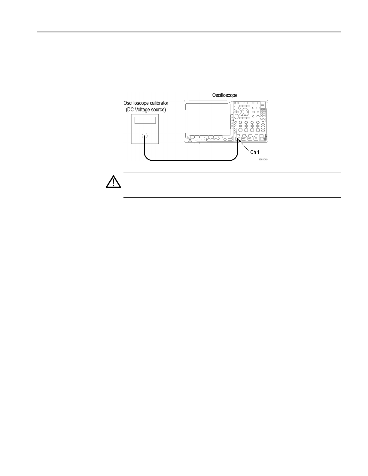
Performance Verification
Check Offset Accuracy
This test check
1. Connect the oscilloscope to a DC voltage source. If you are using the Fluke
9500 calibrat
oscilloscope channel 1.
WAR N ING. The generator is capable of providing dangerous voltages. Be sure to
set the g
the test hookup during the performance of this procedure.
2. Push th
enerator to off or 0 volts before connecting, disconnecting, and/or moving
s the offset accuracy.
or as the DC voltage source, connect the calibrator head to the
e front-panel Default Setup button.
3. Set the Acquisition mode to Average as follows:
a. Push the front-panel Acquire button.
b. Push the Mode lower-bezel button (if not already selected).
c. Push the Av e ra g e side bezel button.
d. Make sure that the number of averages is set to 16.
4. Set
5. Set the Horizontal Scale to 1.00 ms per division.
6. Set the Bandwidth to 20 MHz as follows:
the trigger source to AC line:
a. Push the Trigger Menu front-panel button.
b. Push the Source lower-bezel button.
c. Select the AC Line as the trigger source.
a. Push the channel 1 button.
b. Push the lower-bezel Bandwidth button.
c. Push the side-bezel button to set the bandwidth to 20 MHz.
MDO4000 Series Specifications and Performance Ve rification 71
Page 80

Performance Ve rification
7. Check that the v
a. Push the lower-bezel More button to select Position.
b. In the side-bezel button, check that the Vertical Position is set to 0divs.
c. If it is not 0 divs, turn the Vertical Position knob to set the position to 0.
8. Select 50 Ω impedance as follows:
a. Set the calibrator to 50 Ω output impedance (50 Ω source impedance).
b. Push the channel 1 button.
c. Set the Termination to 50 Ω.
9. Set the vertical Scale to 1mVper division.
10. Set the offset as follows:
a. Set the calibrator to 900 mV vertical offset.
b. Push the lowe r-bezel More button to select Offs
c. Set the Vertical Offset to 900 mV, as shown in the test record.
11. Select the Mean measurement (if not already selected) as follows:
a. Push the front-panel Wave Inspector Measure button.
ertical position is set to 0 divs:
et.
b. Push the Add Measurement lower-bezel button.
c. Select the Mean measurement.
d. Push the OK Add Measurement side-bezel button.
12. View the mean value in the measurement pane at the bottom of the display
and enter it as the test result in the test record.
13. Repeat step 12 for each vertical scale and offset setting combination shown
in the test record.
14. Repeat the tests at 1 MΩ impedance as follows:
a. Change the calibrator impedance to 1 MΩ.
b. Push the front-panel channel 1 button.
c. Set the Termination (input impedance) to
d. Repeat steps 9 through 13.
15. Repeat the p rocedure for all remaining channels as follows:
a. Deselect the channel that you have already tested.
b. Move the DC voltage source connection to the next channel to be tested.
c. Starting from step 6, repeat the procedure for each channel.
1MΩ.
72 MDO4000 Series Specifications and Performance Verification
Page 81

Performance Verification
Check Analog Bandwidth
This test check
s the bandwidth at 50 Ω and 1 M Ω for each channel.
1. Connect the output of the leveled sine wave generator (for example, Fluke
9500) to the os
cilloscope channel 1 input as shown in the following
illustration.
WAR N ING. The generator is capable of providing dangerous voltages. Be sure to
set the generator to off or 0 volts before connecting, disconnecting, and/or moving
the test hookup during the performance of this procedure.
2. Push the front-panel Default Setup button.
3. Select 50 Ω impedance as follows:
a. Set the calibrator to 50 Ω output impedance and to generate a sine wave.
b. Push the front-panel channel 1 button.
c. Set t
he Termination (input impedance) to 50 Ω.
4. Set the Acquisition mode to Sample as follows:
a. Push the front-panel Acquire button.
b. Push the Mode lower-bezel button (if not already selected).
c. Push the Sample side bezel button.
5. Set the Vertical Scale to 1mVper division.
or vertical scales less than 500 mV/div, adjust the signal source to at least
6.F
8 vertical divisions at the selected vertical scale with a set frequency of
50 kHz. For example, at 5 mV/div, use a ≥40 mV
≥16 mV
signal, and at 1 mV/div, use a ≥8mV
p-p
of 500 mV/div and 1 V/div adjust the signal source to 3 V
signal, at 2 mV/div, use a
p-p
signal. For vertical scales
p-p
.Useasinewave
p-p
for the signal source.
7. Set the Horizontal Scale to 10 μs per division.
MDO4000 Series Specifications and Performance Ve rification 73
Page 82

Performance Ve rification
8. Record the peak
-to-peak measurement:
a. Push the front-panel Wave Inspector Measure button.
b. Select the Peak-to-Peak mea surement.
c. Push the OK Add Measurement side-bezel button.
d. This will provide a mean V
of the signal. Call this value V
p-p
in-pp
.
e. Enter this value in the test record.
9. Set the Hor
izontal Scale to 4nsper division.
10. Adjust the signal source to the maximum bandwidth frequency for the
bandwidt
h and model desired, as shown in the following worksheet.
11. Record the peak-to-peak measurement as follows:
a. View the mean V
of the signal. Call this value V
p-p
bw-pp
.
b. Enter this value in the test record.
NOTE. For more information on the contents of this worksheet, refer to the
bandwidth specifications. (See Table 1 on page 1.)
Table 17: Maximum bandwidth frequency worksheet
l: MDO4104-3, MDO4104-6
Mode
Impe
50
dance
ical Scale
Vert
/div — 1 V/div
5mV
/div — 4.98 mV/div
2mV
V/div — 1.99 mV/div
1m
mum bandwidth
Maxi
z
1GH
350 MHz
175 MHz
74 MDO4000 Series Specifications and Performance Verification
Page 83

Performance Verification
Table 17: Maximum bandwidth frequency worksheet (cont.)
Model: MDO4104-3, MDO4104-6
Impedance Vertical Scale Maximum bandwidth
1M
Model: MDO4054-3, MDO4054-6
50 and 1 M
Model: MDO4034-3
50 and 1 M 2 mV/div — 1 V/div
Model: MDO4014-3
50 and 1 M 1 mV/div — 1 V/div
1
For MDO4104-3 and MDO4104-6 performance verification, use 500 MHz, rather than 1 GHz, on the 5 mV/div
vertical scale.
5 mV/div — 1 V/div
2 m V/div — 4.98 mV/div
1 m V/div — 1.99 mV/div
5 mV/div — 1 V/div
2 m V/div — 4.98 mV/div
1 m V/div — 1.99 mV/div
1 m V/div — 1.99 mV/div
500 MHz
350 MHz
175 MHz
500 MHz
350 MHz
175 MHz
350 MHz
175 MHz
100 MHz
1
12. Use the values of V
bw-pp
and V
that you entered in the test record to calculate
in-pp
the Gain at bandwidth with the following equation:
Gain = V
bw-pp
/ V
in-pp
To pass the performance measurement test, Gain should be ≥ 0.707. Enter
Gain in the test record.
13. Repeat steps 5 through 12 for all combinations of Vertical Scale and
Horizontal Scale settings listed in the test record.
14. Repeat the tests at 1 MΩ impedance as follows:
hange the calibrator impedance to 1 MΩ.
a.C
b. Push the front-panel channel 1 button.
c. Set the Termination (input impedance) to 1MΩ.
d. Repeat steps 5 through 13.
15. Repeat the procedure for all remaining channels as follows:
a. Push the front-panel button to deselect the channel that you have already
tested.
b. Move the calibrator connection to the next channel input to be tested.
c. Starting from step 3, repeat the procedure for each input channel.
MDO4000 Series Specifications and Performance Ve rification 75
Page 84

Performance Ve rification
Check Random Noise,
Sample Acquisition Mode
This test check
the oscilloscope for this test.
1. Disconnect ev
2. Push the fron
3. Set Gating to Off as follows:
a. Push the front-panel Wave Inspector Measure button.
b. Push the bottom-bezel More buttontoselectGating.
c. Push the side-bezel Off (Full Record) button.
4. Select the RMS measurement as follows:
a. Push the b
b. Select the RMS measurement.
c. Push the side-bezel OK Add Measurement button.
5. Reset statistics as follows:
a. Push the bottom-bezel More button to select Statistics.
b. Push the side-bezel Reset Statistics button.
s random noise. You do not need to connect any test equipment to
erything from the oscilloscope inputs.
t-panel Default Setup button.
ottom-bezel Add Measurement button.
6. Read a
Val ue ( S M V ) .
7. Set t
a. Push the front-panel Acquire button.
b. Push the bottom-bezel Mode button to display the Acquisition Mode
c. Push the side-bezel Av e rage button.
d. Make sure that the number of averages is set to 16.
8. Reset statistics as follows:
a. Push the front-panel Wave Inspector Measure button.
b. Push the bottom-bezel More button to select Statistics (if it is not already
c. Push the side-bezel Reset Statistics button.
9. Read and make a note of the RMS Mean value. This is the Averaged Mean
Val ue ( A M V ) .
10.
Calculate the RMS noise (RMS noise = SMV – AMV), and enter the
calculated RMS noise in the test record.
nd make a note of the RMS Mean value. This is the Sampled Mean
he Acquisition mode to Average as follows:
menu (if it is not already selected).
selected).
76 MDO4000 Series Specifications and Performance Verification
Page 85

Performance Verification
11. Set the Acquisi
a. Push the front-panel Acquire button.
b. Push the Mode lower-bezel button (if it is not already selected).
c. Push the Sample side bezel button.
12. Repeat the tests at 50 Ω as follows:
a. Push the front-panel channel 1 button.
b. Set the Te r
c. Push the front-panel Wave Inspector Measure button, and repeat steps 5
through 1
13. Repeat the tests at 250 MHz bandwidth a s follows:
a. Push the front-panel channel 1 button.
b. Set the Termination (input impedance) to 1MΩ.
c. Push the bottom-bezel Bandwidth button.
d. Push the side-bezel 250 MHz button.
e. Push t
tionmodetoSampleasfollows:
mination (input impedance) to 50 Ω.
1.
he front-panel Waveform Inspector Measure button.
f. Repeat steps 5 through 12.
14. Repeat the tests at 20 MHz bandwidth as follows:
a. Push the front-panel channel 1 button.
b. Set the Termination (input impedance) to 1MΩ.
c. Push the bottom-bezel Bandwidth button.
sh the side-bezel 20 MHz button.
d. Pu
e. Push the front-panel Waveform Inspector Measure button.
f. Repeat steps 5 through 12.
15. Repeat the procedure for all remaining channels as follows:
a. Push the front-panel button to deselect the channel that you have already
tested.
b. Starting from step 3, repeat the procedure for each input channel.
MDO4000 Series Specifications and Performance Ve rification 77
Page 86

Performance Ve rification
Check Sample Rate and
Delay Time Accuracy
This test check
s the sample rate and delay time accuracy (time b ase).
1. Connect the output of a time mark generator to the oscilloscope channel
1 input using a
50 Ω cable, as shown in the following illustration.
WARNING. The generator is capable of providing dangerous voltages. Be sure to
set the generator to off or 0 volts before connecting, disconnecting, and/or moving
the test hookup during the performance of this procedure.
2. Set the time mark generator period to 80 ms. Useatimemarkwaveform
with a fast rising edge.
3. Push the front-panel Default Setup button.
4. Set the impedance to 50 Ω as follows:
a. Push the front-panel channel 1 button.
b. Set the Termination to 50 Ω.
5. If it is adjustable, set the time mark amplitude to approximately 1V
p-p
.
6. Set the Vertical Scale to 500 mV per division.
7. Set the Horizontal Scale to 20 ms per division.
8. Adjust the Vertical Position knob to center the time mark signal on the screen.
9. Adjust the Trigger Level as necessary for a triggered display.
10. Adjust the Horizontal Position to move the trigger location to the center of
the screen (50%).
11. Set the delay to 80 ms as follows:
a. Push the front-panel Acquire button.
b. Push the lower-bezel Delay buttontoturndelayon(ifitisnotalreadyon).
c. Turn the Horizontal Position knob clockwise to set the delay to exactly
80 ms.
78 MDO4000 Series Specifications and Performance Verification
Page 87

Performance Verification
12. Set the Horizon
13. Compare the rising edge of the marker with the center horizontal graticule
line. The risi
the deviation in the test record.
NOTE. One division of displacement from graticule center corresponds to a
5 ppm time base error.
tal Scale to 400 ns/div.
ng edge should be within ±1 divisions of center graticule. Enter
MDO4000 Series Specifications and Performance Ve rification 79
Page 88

Performance Ve rification
Check Delta Time
Measurement Accuracy
This test check
instrument setting and input signal.
Connect a 50 Ω c
as shown in the following illustration.
WARNING.
set the generator to off or 0 volts before connecting, disconnecting, and/or moving
the test hookup during the performance of this procedure.
2. Push the oscilloscope front-panel Default Setup button.
s the Delta-time measurement accuracy (DTA) for a given
oaxial cable from the signal source to the oscilloscope channel 1,
The generator is capable of providing dangerous voltages. Be sure to
3. Select
a. Set the sine wave generator output impedance to 50 Ω.
b. Push the channel 1 button to display the channel 1 menu.
c. Set the Termination (input impedance) to 50 Ω.
4. Set the trigger source to channel 1 as follows:
a. Push the Trigger Menu button.
b. Pus
c. Select channel 1 (if not already selected).
5. Set the Mean & St Dev Samples to 100 as follows:
a. Push the Wave Inspector Measure button.
b. Push the bottom-bezel Add Measurement button.
c. Select the Burst Width measurement.
d. Push the side-bezel OK Add Measurement button.
e. Push the bottom-bezel More button to select Statistics.
f. Set the Mean & Std Dev Samples to 100, as shown in the side menu.
50 Ω impedance as follows:
htheSource lower-bezel button (if not already selected).
80 MDO4000 Series Specifications and Performance Verification
Page 89

Performance Verification
6. Set the signal s
NOTE. To provide consistent results, set the signal source frequency such that the
zero crossing does not occur at the beginning or end of the record.
7. Set the Horizontal Scale to 4nsper division.
8. Set the Vert
9. Record the Std Dev value as follows:
a. Push the side-bezel Reset Statistics button.
b. Push the Menu button to remove the side-bezel menu.
c. Wa i t five or 10 seconds for the oscilloscope to acquire all of the samples.
d. Verify that the Std Dev is less than the upper limit shown in the test record.
e. Enter t
10. Repeat steps 6 through 9 for each setting combination shown in the test record.
11. Repeat the procedure for all remaining channels as follows:
a. Push the front-panel button to deselect the channel that you have already
tested.
ource to 240 MHz and 40 mV as shown in the test record.
ical Scale to 5mVper division.
he reading in the test record.
b. Connect the signal source to the input for the next channel to be tested.
c. Repeat the procedure from step 3 until all channels have been tested.
MDO4000 Series Specifications and Performance Ve rification 81
Page 90

Performance Ve rification
Check Digital Threshold
Accuracy
This test check
applies to digital channels D0 through D15, and to channel threshold values of
0Vand+4V.
1. Connect the P6616 digital probe to the oscilloscope, as shown in the following
illustration:
a. Connect the DC voltage source to the digital channel D0.
b. If you are us
connect the calibrator head to the digital channel D0, using the
BNC-to-0.1 inch pin adapter listed in the Required Equipment table. (See
Table 15 on page 28.)
c. Connect channel D0 to both the corresponding signal pin and to a ground
pin on the adapter.
s the threshold accuracy of the digital channels. This procedure
ing the Fluke 9500 calibrator as the DC voltage source,
WARNING. The generator is capable of providing dangerous voltages. Be sure to
set the generator to off or 0 volts before connecting, disconnecting, and/or moving
the test hookup during the performance of this procedure.
2. Turn on the d igital channels as follows:
a. Push the front-panel D15-D0 button.
b. Push the D15-D 0 On/Off lower-bezel button.
c. Push the Tu rn On D7 - D0 and the Turn On D15 - D8 side-bezel buttons
to turn these channels On.
d. Make sure that the side-bezel Display selection is On.
e. The instrument will display the 16 digital channels.
82 MDO4000 Series Specifications and Performance Verification
Page 91

Performance Verification
3. Set the channel
threshold to 0 V as follows:
a. Push the Thresholds lower-bezel button (if not already selected).
b. Select channel D0.
c. Set the value to 0.00 V (0 V/div), using the coarse and fine settings of the
knob as necessary to set the exact value.
4. Push the Menu button and then set the Horizontal Scale to 4μs per division.
5. Set the Trigger source as follows:
a. Push the front-panel Trigger Menu button.
b. Push the Source lower-bezel button (if not already selected).
c. Select channel D0.
6. Set the DC voltage source (Vs) to -400 mV. Wait 3 seconds. Check the logic
level of the channel D0 signal display. If it is at a static logic high, change the
DC voltage source Vs to -500 mV.
7. Increment Vs b y +10 mV. Wait 3 seconds and check the logic level of the
channel D0 signal display. If it is a static logic high, record the Vs value
as in the 0 V row of the test record.
If the signal level is a logic low or is alternating between high and low, repeat
this step (increment Vs by 10 mV, wait 3 seconds, and check for a static logic
high) until a value for V
is found.
s-
8. Click the lower-bezel Slope button to change the slope to Falling.
9. Set the DC voltage source (Vs) to +400 mV. Wait 3 seconds. Check the logic
level of the channel D0 signal display.
If it is at a static logic low, change the DC voltage source Vs to +500 mV.
10. Reduce Vs by -10 mV. Wait 3 seconds and check the logic level of the channel
D0 signal display. If it is a static logic low, record the Vs value as V
in the
s+
0 V row of the test record.
If the signal level is a logic high or is alternating between high and low, repeat
this step (decrement Vs by 10 mV, wait 3 seconds, and c h eck for a static logic
low) until a value for V
11. Find the average using this formula: V
is found.
s+
=(Vs-+Vs+)/2. Record the average
sAvg
as the test result in the test record.
Compare the test result to the limits. If the result is between the limits,
continue with the procedure to test the channel at the +4 V threshold value.
12. Set the channel threshold to +4 V as follows:
a. Push the front-panel D15-D0 button.
b. Push the Thresholds lower-bezel button.
MDO4000 Series Specifications and Performance Ve rification 83
Page 92

Performance Ve rification
c. Select channel
D0.
d. Push the Fine front-panel button to turn off the fine adjustment.
e. Set the value near 4.00 V (4 V/div).
f. Push the Fine buttontoturnthefine adjustment on again.
g. Set the value to exactly 4.00 V (4 V/div).
13. Set the DC voltage source (Vs) to +4.4 V. Wait 3 seconds. Check the logic
levelofthechannelD0signaldisplay.
14. Decrement Vs by -10 mV. Wait 3 seconds and check the logic level of the
channel D0 signal display. If it is a static logic low, record the Vs value as
V
in the 4 V row of the test record.
s+
If the signal level is a logic high or is alternating between high and low, repeat
this step (decrement Vs by 10 mV, wait 3 seconds, and check for a static logic
low) until a value for V
is found.
s+
15. Push the front-panel Trigge r M e n u button.
16. Click the lower-bezel Slope button to change the slope to Rising.
17. Set the DC voltage source (Vs) to +3.6 V. Wait 3 seconds. Check the logic
levelofthechannelD0signaldisplay.
If the signal level is a static logic high, change the DC voltage source Vs to
+3.5 V.
18. Increment Vs by +10 mV. Wait 3 seconds and check the logic level of the
channel D0 signal display. If it is a static logic high, record the Vs value as
in the 4 V row of the test record.
V
s-
If the signal level is a logic low or is alternating between high and low, repeat
this step (increment Vs by 10 mV, wait 3 seconds, and check for a static logic
high) until a value for V
19. Find the average using this formula: V
is found.
s-
=(Vs-+Vs+)/2. Record the average
sAvg
as the test result in the test record.
Compare the test result to the limits. If the result is between the limits, the
channel passes the test.
20. Repeat the procedure for all remaining digital channels as follows:
a. Push the D15–D0 button.
b. Move the DC voltage source connection, including the ground lead, to the
next digital channel to be tested.
c. Starting from step 3, repeat the procedure until all 16 digital channels
have been tested.
84 MDO4000 Series Specifications and Performance Verification
Page 93

Performance Verification
Check Phase Noise
This step check
checks at three offset frequencies: 10 kHz, 100 kHz, and 1 MHz.
WAR N ING. The generator is capable of providing dangerous voltages. Be sure to
set the generator to off or 0 volts before connecting, disconnecting, and/or moving
the test hookup during the performance of this procedure.
NOTE. Do not use an N connector with the Anritsu generator. Equipment damage
will result if an N connector is used.
1. Connect the output of a signal generator, such as the Anritsu generator, to the
oscilloscope RF Input, using a 50 Ω SMA coaxial cable (see the following
figure).
s the phase noise measured offset from a 2 GHz CW signal . It
2. Set the generator for a 2 GHz, 0 dBm signal.
3. Initial oscilloscope setup:
a. Push the front-panel Default Setup button.
b. Turn Channel 1 off.
c. Push the front-panel RF button to turn on the RF channel and display
the bottom-bezel RF menu.
d. Turn on the average trace as follows: Push the bottom-bezel Spectrum
Traces button. Push the side-bezel Avera g e button to set the Average
Traces to On. Push the side-bezel Normal button to set Normal to Off.
e. Set the center frequency to 2 GHz as follows: Push the front-panel
Freq/Span button. Push the side-bezel Center Frequency button. Set the
center frequency to 2 GHz.
f. Set the span to 50.0 kHz as follows: Set the Span to 50.0 kHz.
g. Center the signal on the display. To do this:
MDO4000 Series Specifications and Performance Ve rification 85
Page 94

Performance Ve rification
Push the Marker
Push the RToCenterside-bezel button.
h. Set the resolution bandwidth (RBW) to 250 Hz as follows: Push the
front-panel BW button. Push the side-bezel RBW Mode button to set the
RBW mode to M
i. Set the markers to delta as follows: Push the front-panel Markers button.
Push the sid
On. Push the side-bezel Readout button to selec t Delta.
j. Set the ref
button. Push the side-bezel Ref Level button. Set the reference level to
0dBm.
4. Check at 10 kHz:
a. Push the
b. Set marker a to the signal peak.
c. Set marker b to 10 kHz as shown in the following figure.
erence level to 0 dbm as follows: Push the front-panel Ampl
front-panel Markers button.
s front-panel button.
anual. Set the resolution bandwidth to 250 Hz.
e-bezel Manual Markers button to set the manual markers to
d. Note the bottom value in the marker b readout (in dBc/Hz) and enter it in
the test record.
5. Repeat the check at 100 kHz:
a. Change the span to 500 kHz.
b. Change the resolution bandwidth (RBW) to 1 kHz.
c. Set marker a to the signal peak.
86 MDO4000 Series Specifications and Performance Verification
Page 95

Performance Verification
d. Set marker b to 1
e. Note the bottom value in the marker b readout (in dBc/Hz) and enter it
in the test rec
given in the test record.
6. Repeat the c
a. Changethespanto5MHz.
b. Change the resolution bandwidth (RBW) to 50 kHz.
c. Set marker a to the signal peak.
d. Set marker b to 1 MHz.
e. Note the bottom value in the marker b readout (in dBc/Hz) and enter it
in the test record. Make sure that the instrument meets the specification
given in the test record.
heck at 1 MHz:
00 kHz.
ord. Make sure that the instrument meets the specification
MDO4000 Series Specifications and Performance Ve rification 87
Page 96

Performance Ve rification
Check Disp layed Average
Noise Lev el (DANL)
This test does n
The test measures the average internal noise level of the instrument, ignoring
residual spur
It checks four ranges:
50kHzto5MHz(allmodels)
5MHzto3GHz(allmodels)
3 GHz to 4 GHz (MDO4104-6 and MDO4054-6 only)
4 GHz to 6 GHz (MDO4104-6 and MDO4054-6 only)
NOTE. If the specific measurement frequency results in measuring a residual spur
that is visible above the noise level, the DANL specification applies not to the
spur but to the noise level on either side of the spur. Please refer to the Spurious
Response specifications. (See page 19.)
ot require an input signal.
s.
88 MDO4000 Series Specifications and Performance Verification
Page 97

Performance Verification
1. Initial oscill
a. Terminate the RF input in 50 Ω and make sure that no input signal is
applied.
b. Push the front-panel Default Setup button.
c. Turn channel 1 off.
d. Push the front-panel RF button to turn on the RF channel and display
the bottom-bezel RF menu.
e. Turn on the average trace as follows: Push the bottom-bezel Spectrum
Traces button and set Normal to Off. Push the side-bezel Av e r ag e button
to set the Average Traces to On.
f. Turn on the average detection as follows: Push the bottom-bezel
Detection Method button. Push the side-bezel button to set the detection
method t
detection method to Average.
g. Set the
Ampl button. Push the side-bezel Ref Level button. Set the Ref Level to
–25.0 dBm.
h. Set the start and stop frequency as follows: Push the front-panel
Freq/Span button. Push the side-bezel Start button. Set the start
frequency to 50 kHz. Push the side-bezel Stop button. Set the stop
frequency to 5 MHz.
oscope setup:
o Manual. Push the side-bezel Average Trace button. Set the
reference level to –25.0 dBm as follows: Push the front-panel
2. Check from 50 kHz to 5 MHz (all models):
a. Set Manual Marker (a) at the frequency with the highest noise level
as follows: Push the Markers front-panel button. Push the Manual
Markers side bezel button to turn o n the markers. Turn Multipurpose
knob a to move the marker to the frequency at the noise threshold (highest
oint of noise), ignoring any spurs. For this span, it should be at 50 kHz
p
on the far left of the screen. See the following figure.
MDO4000 Series Specifications and Performance Ve rification 89
Page 98

Performance Ve rification
b. Record the noise threshold value (in dBm/Hz) in the test record and
compare it to the instrument specification.
3. Check from 5 MHz to 3 GHz (all models):
a. Set the s
b. Set the start frequency to 5 MHz.
c. Set Manual Marker (a) at the fre quency of the highest noise, ignoring
any spurs.
d. Set the center frequency as follows: Push the RToCenterside-bezel
button.
e. Set the span to 10 MHz as follows: Push the side-bezel Span button. Set
the Span to 10 MHz.
f. Record the highest noise value (in dBm/Hz) in the test record and compare
it to the instrument specification.
4. Check from 3 GHz to 4 GHz (MDO4104-6 and MDO4054-6 only):
a. Set the stop frequency to 4 GHz.
b. Set the start frequency to 3 GHz.
c. Set Manual Marker (a) at the fre quency of the highest noise, ignoring
any spurs.
top frequency to 3 GHz.
d. Set the center frequency as follows: Push the RToCenterside-bezel
button.
90 MDO4000 Series Specifications and Performance Verification
Page 99

Performance Verification
e. Set the span to 1
theSpanto10MHz.
f. Record the hig
it to the instrument specification.
5. Check from 4
a. Set the stop frequency to 6 GHz.
b. Set the start frequency to 4 GHz.
c. Set Manua l Marker (a) at the frequency of the highest noise , ignoring
any spurs.
d. Set the center frequency as follows: Push the RToCenterside-bezel
button.
e. Set the span to 10 MHz as follows: Push the side-bezel Span button. Set
theSpanto10MHz.
f. Record the highest noise value (in dBm/Hz) in the test record and compare
it to the instrument specification.
0 MHz as follows: Push the side-bezel Span button. Set
hest noise value (in dBm/Hz) in the test record and compare
GHz to 6 GHz (MDO4104-6 and MDO4054-6 only):
MDO4000 Series Specifications and Performance Ve rification 91
Page 100

Performance Ve rification
Check Level Measurement
Uncertainty
This test check
+10 dBm, 0 dBm, and –15 dBm. This check uses the generator to step frequencies
across four spans to verify that the instrument meets the specification.
For this check, you will need the following equipment, which is described in the
Required Equipment table. (See Table 15 on p age 28.)
Generator, such as the Anritsu generator
Power meter
Power head
Power splitter
Adapters and cables as shown in the following figure.
WARNING. The generator is capable of providing dangerous voltages. Be sure to
set the generator to off or 0 volts before connecting, disconnecting, and/or moving
t hookup during the performance of this procedure.
the tes
NOTE. Use an SMA connector with the Anritsu generator. Equipment damage
esult if an N connector is used.
will r
s the level measurement uncertainty at three reference levels:
1. Connect the equipment as shown in the following figure.
2. Initial oscilloscope setup:
ush the front-panel Default Setup button.
a.P
b. Turn Channel 1 off.
c. Push the front-panel RF buttontoturnontheRFchannel.
92 MDO4000 Series Specifications and Performance Verification
 Loading...