

Page 1

xx
Tektronix MDO Demo 1 Board
ZZZ
Instruction Manual
www.tektronix.com
*P071292400*
071-2924-00
Page 2

Copyright © Tektronix. All rights reserved. Licensed software products are owned by Tektronix or its subsidiaries or suppliers, and are
protected by na
tional copyright laws and international treaty provisions.
Tektronix pro
previously published material. S pecifications and price change privileges reserved.
TEKTRONIX and TEK are registered trademarks of Tektronix, Inc.
ducts are covered by U.S. and foreign patents, issued and pending. Information in this publication supersedes that in all
Contacting Tektronix
Tektronix, Inc.
14150 SW Karl Braun Drive
P.O. Box 500
Beaverton, OR 97077
USA
For product information, sales, service, and technical support:
In North America, call 1-800-833-9200.
Worldwide, visit www.tektronix.com to find contacts in your area.
Page 3

Table of Contents
Preface................................................................................................................................. ii
Compliance I
Installati
Operation............................................................................................................................... 3
Signal Descriptions .. .. . .. . ... ... . .. . .. . .. . .. . .. . .. . . .. . .. . .. . .. . .. . .. . .. . ... ... . .. . .. . .. . .. . .. . .. . ... ... . .. . .. . .. . .. . .. . .. . . . . . ....... 5
nformation............................................................................................................... ii
Environmental Considerations................................................................................................... ii
Preventing Electrostatic Damage................................................................................................ ii
on..............................................................................................................................1
Table of Content
s
Tektronix MDO Demo 1 Board Instruction Manual i
Page 4

Compliance Info
rmation
Preface
The MDO Demo 1 board provides signals that you can use to show key features of Tektronix MDO4000 Series oscilloscopes.
Compliance Information
Environmental Considerations
This section provides information about the environmental impact of the product.
Product End-of-Life Handling
Observe the following guidelines when recycling an instrument or component:
Equipmen
may contain substances that could be harmful to the environment or human health if improperly handled at the product’s
end of life. In order to avoid release of such substances into the environment and to reduce the use of natural resources,
we encou
or recycled appropriately.
t recycling.
rage you to recycle this product in an appropriate manner that will ensure that most of the materials are reused
This sym
to Directives 2002/96/EC and 2006/66/EC on waste electrical and electronic equipment (WEEE) and
batteries. For information about recycling options, check the Support/Service section of the Tektronix Web
site (w
Production of this equipment required the extraction and use of natural resources. The equipment
bol indicates that this product complies with the applicable European Union requirements according
ww.tektronix.com).
Restriction of Hazardous Substances
This product has been classified as Monitoring and Control equipment, and is outside the scope of the 2002/95/EC RoHS
Directive.
Preventing Electrostatic Damage
trostatic discharge (ESD) can damage components on the demo board. To prevent ESD:
Elec
ot touch exposed components or connector pins unless you are using ESD protective measures, such as wearing
Do n
an antistatic wrist strap.
Handle the demo board as little as possible.
Do not slide the demo board over any surface.
Transport and store the demo board in a static-protected bag or container.
ii Tektronix MDO Demo 1 Board Instruction Manual
Page 5

Installation
1. Plug the dual USB A connectors from
one end of the “
comes with your board, into two USB
ports of a PC or an oscilloscope. Do
this before p
connector from the other end of the U SB
cable into the MDO Demo 1 board.
You need to a
connectors to provide adequate power
to the demo board.
2. Plug the single B connector from the
other end of the USB cable into the demo
board. Two green and one red LEDs
on the board turn on and remain steady
when you apply adequate power to the
board.
If you plug the single B connector to the
demo board when there is just one of the
two USB A connectors attached to the
PC or oscilloscope, you may cause an
over-current (>500 mA) condition. This
can generate an error message.
Installation
T” USB cable, which
lugging the single USB B
ttach both USB A
3. Connect the MDO4000 Series
oscilloscope RF input to the MDO Demo
1 Board RF output using the N-to-BNC
Adapter (103–0045–00) and a 50 Ω coax
BNC cable.
Tektronix MDO Demo 1 Board Instruction Manual 1
Page 6

Installation
4. Connect one or more analog probes,
if desired, from the MDO4000 Series
oscilloscope
to the desired connector or
connectors on the Demo 1 Board.
NOTE. The Tektronix MDO Demo 1 board requires approximately 0.75 A to operate.
NOTE. The purpose of the USB cable is to provide power to the demo board. No communication occurs over the USB cable.
All available signals (except for single-shot) are present on their connectors when you apply power to the demo board.
Push the RESET button immediately after connecting power.
2 Tektronix MDO Demo 1 Board Instruction Manual
Page 7

Operation
The MDO4000 Series oscilloscope has six setups of product dem onstrations, all of which utilize the MDO 1 Demo Board.
Use these setups for the:
Multiple peaks demo
Spectrogram demo
VCO/PLL Turn On demo
ASK Modulation demo
Frequency Hop demo
Capture Bandwidth demo
To use these setups and see related demo instructions, do the following:
1. Push the front-panel Utility button of your
MSO4000 Series oscilloscope.
Operation
2. Push Utility Page
3. Turn multipurpose knob a and select Demo.
4. Push the desired demo from the
bottom-bezel menu.
Follow the probe setup instructions for the
related demo that now appear on the screen.
5. Push Recall Demo Setup from the side
menu to automatically setup the oscilloscope
optimally for the demo.
6. Push the button marked Mode on the
MDO Demo 1 Board as many times as
needed to light up the red LED on the board
corresponding to the demo you wish to run.
Utility
Page
Demo
Utility
Page
Demo
Multiple
Peaks
Spectro-
gram
VCO/PLL
Turn On
ASK
Modulation
Frequency
Hop
Capture
Bandwidth
The board does the following, depending on the mode selected:
Tektronix MDO Demo 1 Board Instruction Manual 3
Page 8

Operation
CW (Continuous Wave) Demo
The RF output connector generates a CW signal at 2.4 GHz.
The red LED labeled “CW” at grid location B11 turns on.
NOTE. There is no corresponding demo setup in the oscilloscope for this mode.
Multiple Peaks Demo
The RF output connector generates an array of frequencies, which are centered around 2.4 GHz, to show the ability of
the MDO4000 Series oscilloscopes to dynamically mark each peak in the frequency domain with its exact frequency
and amplit
ude.
The red LED
labeled “Multiple Peaks” at grid location B11 turns on.
Spectrogram Demo
The RF output connector generates an array of frequencies, which are centered around 2.4 GHz and are both amplitude and
frequency modulated, to show the value of the Spectrogram function on slowly changing RF phenomena.
The red LED labeled “Spectrogram” at grid location B11 turns on.
VCO/PLL Turn On Demo
The RF output connector, VCO-1 Enable loop, and PLL-1 Voltage loop, and the SPI, CLK, SPO_SS_1, and SPO_MOSI
pin connectors generate signals that show the interaction between the control signals and the latency of the RF
square
output turning on and tuning to the desired frequency. Use this mode with the VCO-1 On/Off push button, which toggles
the state of the VCO-1 on and off.
The red LED labeled “VCO/PLL-1 Turn On” at grid B11 turns on.
ASK M
The RF output connector generates an RF signal, which is centered at 2.4 GH,z and is amplitude-modulated by a control
signal that turns the RF output on and off. View the control signal and a trigger signal by connecting analog channels to the
ASK_MOD probe loop and the Trigger loop.
odulation Demo
The red LED labeled “ASK Modulation” at grid B12 turns on.
Frequency Hop Demo
The RF output connector generates three frequency steps. These are centered at 2.4 G Hz and step up and down 3 MHz from
e CF (center frequency). By using the built-in RF Frequency versus Time function of the MDO4000 Series oscilloscopes,
th
you can see the frequency hop represented as a real-time waveform in the time domain.
The red LED labeled “Frequency Hop” at grid B12 turns on.
4 Tektronix MDO Demo 1 Board Instruction Manual
Page 9

Capture BW Demo
The RF output connector generates both a 2.4 GHz signal and a 900 MHz signal simultaneously to show the broad
frequency capture capability.
The red LED labeled “Capture BW” at grid B12 turns on.
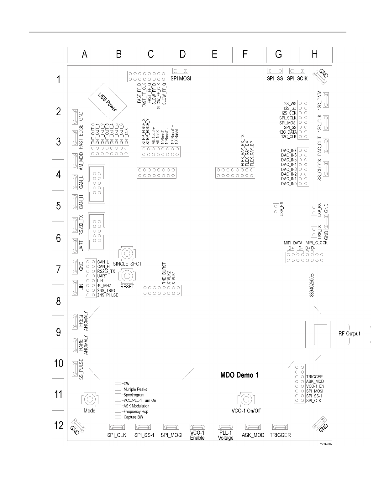
Signal D escriptions
Signal Descript
ions
The followi
up the connector grid location in the following S ignal Descriptions section and use the grid location information to find the
signal on the demo board.
ng diagram includes a grid to help you locate signal outputs. To find a particular signal output on the board, look
Tektronix MDO Demo 1 Board Instruction Manual 5
Page 10
Signal Descript
ions
6 Tektronix MDO Demo 1 Board Instruction Manual
Page 11

2nsPulse
Board label: 2NS_PULSE
Grid location: A8
Description: This signal is a 2 ns to 3 ns, 2.5 V pulse at a 3.3 ms repetition rate. Use this signal to show the minimum pulse
width capture specification of an instrument digital acquisition system.
2 ns Pulse Trigger
Board label: 2NS_TRIG
Grid locati
Description: This is the trigger edge signal for the 2 ns pulse. A falling edge on this signal occurs approximately 5 ns
before the 2 ns pulse.
on: A8
40 MHz
Board label: 40_MHZ
Grid location: A8
Signal Descript
ions
Description: This is a 40 MHz square wave signal.
AM Modulation
Board label: AM_MOD
Grid location: A4
Description: This is a 1.25 MHz carrier amplitude signal modulated by a 1.25 kHz sine wave signal.
The AM Mod signal is centered around ground.
Set the oscilloscope trigger level to either the top or bottom of the waveform to stabilize it on the display.
ASK_MOD
Board label: ASK_MOD
d location: F12, H11
Gri
Description: This is a digital modulation signal that is used to amplitude modulate the RF output when the board is in the
ASK Modulation demo mode. When it is high, the RF is on. When it is low, the RF is off
CAN Bus
Board label: CAN_H, CAN_L
Grid location: A4, A5, A7
Description: These are the CAN (Controller Area Network) bus signals between two CAN transceivers.
The bit rate of the data packet is 500 kbps.
Tektronix MDO Demo 1 Board Instruction Manual 7
Page 12

Signal Descript
ions
Counter Clock
Board label: CNT_CLK
Grid location: B3
Description: This is the 1.25 MHz clock signal for the 7-bit Counter Output described next.
Counter Output Bits
Board label
Grid location: A3, B3
Description: These are the 7-bits of the binary counter. The LSB is CNT_OUT_0. It runs at 625 KHz, which is half of the
counter input clock.
The Counter Output Bits and the Counter Clock signals are on eight adjacent sets of header pins for easy connection to a
digital pr
: CNT_OUT_0: CNT_OUT_6
obe.
Crosstalk
Board label: XTALK1, XTALK2
Grid location: D8
Description: These two signals have significant crosstalk between them. Use them to show MagniVu.
DAC Input, Parallel
Board label: DAC_IN0, DAC_IN1, DAC_IN2, DAC_IN3, DAC_IN4, DAC_IN5, DAC_IN6, DAC_IN7
cation: H3, H4
Grid lo
ption: These signals are the input to the DAC. These are also the 8-bit parallel output signals of the port expander
Descri
in the middle of the mixed signal chain. The sine wave data from the SPI bus is converted to 8 parallel bits to drive the
DAC. DAC_IN0 is the LSB. (See Figure 1.)
See the SPI Bus description for packet details.
8 Tektronix MDO Demo 1 Board Instruction Manual
Page 13
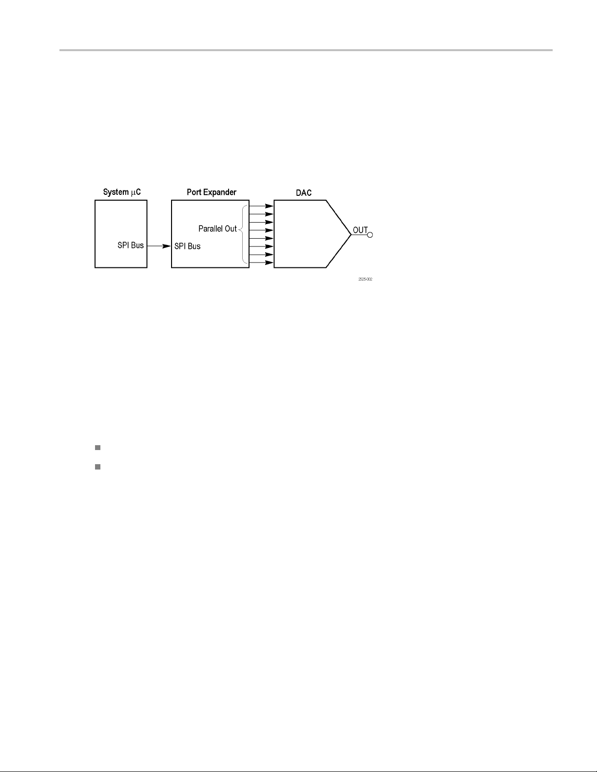
DAC Output
Board label: DAC_OUT
Grid location: H3
Description: This is the output of the DAC at the end of the mixed signal chain. The DAC is driven from the port expander.
The DAC output is a sine wave. Since the output is not filtered, the digitizing levels are present in the output waveform.
(See Figure 1.)
The resulting DAC voltage is a sine wave with an amplitude 0 to 3 volts, and a period of 31 ms.
Figure 1: Mixed signal chain block diagram
Signal Descript
ions
Ethernet Bus
Board label: 10BaseT+, 10BaseT-, 100BaseT+, 100BaseT-
Grid location: C3, D3
Description: These signals generate representative and compliant Ethernet traffic, but the board will not recognize or
commun
pairs:
icate with any externally connected hardware. The followi ng Ethernet Serial Bus signals are driven as differential
The 10Base-T signal pair communicates at a 10 Mbit/s data rate.
The 100Base-TX signal pair communicates at 100 Mbit/s.
Fast Edge
Board label: FAST_EDGE
Grid location: A3
Description: This is a 156 kHz, capacitively-coupled pulse signal with a 1.5 ns rise and fall time.
Fast FF Clock
ard label: FAST_FF_CLK
Bo
Grid location: C1
Description: This is the 1.25 MHz clock input signal to a fairly fast flip-flop. The pulse width of this clock signal varies slowly.
Tektronix MDO Demo 1 Board Instruction Manual 9
Page 14

Signal Descript
ions
Fast FF Data
Board label: FAST_FF_D
Grid location: C1
Description: This is the 1.25 MHz data input signal to a fairly fast flip-flop that is asynchronous to the clock input.
Fast FF Q Output
Board label: FAST_FF_Q
Grid locati
on: C1
Descriptio
n: This is the Q output signal of the fairly fast flip-flop. This signal shows metastable behavior infrequently.
FlexRay
Board label: FLEXRAY_BP, FLEXRAY_BM, FLEXRAY_RX/TX
Grid location: F4
Description: These FlexRay signals consist of the following test points:
FlexRay_BP, the positive half of a differential FlexRay bus
FlexRay_BM, the negative half of a differential FlexRay bus
FlexRay_Rx/Tx, the single-ended logic signal between the controller and the transceiver
The data rate is at 10 Mb/s. The swing is 0 to 3.3 V. Tri-state is at 1.65 V (BP and BM only). There are 15 individual
198-bit long frames.
Frequent Anomaly
abel: FREQ_ANOMALY
Board l
Grid location: A9
Description: There are two frequently occurring anomalies in this pulse train.
A half height runt signal occurs approximately every 104.8 ms. Use a Runt trigger to isolate the signal.
A 25 ns (narrow) pulse appears approximately every 104.8 ms. Use a Pulse Width trigger to isolate the signal.
The pulse train is a repeating group of three pulses. The three pulses are 100 ns, 200 ns, and 100 ns wide, with a 100 ns low
between. The group repeats at a 1.6 μs rate.
The anomaly is a group of four pulses. The four pulses are 100 ns, 50 ns (narrow), 100 ns (runt), and 100 ns wide, with a
ns low between, except for a 50 ns low before the runt.
100
10 Tektronix MDO Demo 1 Board Instruction Manual
Page 15

I2CBus
Board label: I2C_CLK, I2C_DATA
Grid location: H2, H3
Signal Descript
ions
Description: ThesearetheI
There are several different types of data packets.
The clock rate is a 200 kHz, 0 to 5 volt signal.
2
I2S (Inter-IC Sound) Bus
Board labe
Grid location: H2
Description: This is an I2S (Inter-IC sound) serial bus.
The clock rate is 2.5 MHz.
l: I2S_SCK, I2S_WS, I2S_SD
LIN Bus
Board label: LIN
Grid location: A8
Description: This is the LIN (Local Interconnect Network) bus signal between two LIN transceivers.
The bus speed is 19.2 kbaud. It contains a mix of version 1.x and 2.x frames.
C (Inter-IC Communication) bus signals between the μC and a serial EEPROM.
MIL-STD-1553
abel: MIL1553+, MIL1553-
Board l
Grid location: C3
Description: These signals are representative of MIL-STD-1553 bus protocol traffic for a serial, differential pair running at
1 MHz. Messages consist of one or more 16-bit words, where each word is preceded by a 3 μs sync pulse and followed
dd parity bit.
by an o
MIPI_DATA, MIPI_CLOCK
Board label: MIPI_DATA, MIPI_CLOCK
Grid location: H7
Description: These signals are representative of MIPI D-PHY bus protocol traffic for a serial differential pair r unning
at 500 Mb/s.
Tektronix MDO Demo 1 Board Instruction Manual 11
Page 16

Signal Descript
ions
Mode Button
Board label: Mode
Grid location: A11
Description: Push this button to choose which of the seven alternative signals to send out of the RF output connector. Your
current choice is identified by which of the seven related red LEDs is lighted.
PLL-1 Voltage
Board label
Grid location: E12
Description: This signal is the voltage on the first PLL/VCO in the RF section of the board. It typically operates at 2.4 GHz.
: Voltage
Random Burst
Board label: RND_BURST
Grid location: C8
Description: This signal produces bursts of 100 ns wide logic pulses every 6.6 ms. The pattern is a pseudo-random bit
sequence that repeats every 128 bursts and has a 6.32 μs duration.
Rare Anomaly
Board label: RARE_ANOM
Grid location: A10
Description: The two less-frequent anomalies in this pulse train can show up on high waveform capture rate oscilloscopes.
A half-height runt signal occurs approximately every 838.8 ms. Use a Runt trigger to isolate the signal.
A 25 ns (narrow) pulse appears in approximately 838.8 ms. Use a Pulse Width trigger to isolate the signal.
The pulse train is a repeating group of three pulses. The three pulses are 100 ns, 200 ns, and 100 ns wide, with a 100 ns low
en each pulse. The group repeats at a 1.6 μs rate.
betwe
omaly is a group of four pulses. The four pulses are 50 ns, 25 ns (narrow), 100 ns (runt), and 100 ns wide, with a
The an
100 ns low between each pulse, except for a 25 ns low before the narrow pulse.
Reset Button
Board label: RESET
Grid location: B7
Description: Push this button to start all generated signals from a common point.
12 Tektronix MDO Demo 1 Board Instruction Manual
Page 17

RF Output
Board label: None
Grid location: H9
Description: Use the RF output from this connector in the seven different RF demos controlled by the Mode button. Directly
connect this output to the RF input of the MDO4000 Series oscilloscope.
RS232 UART, Transmit
Board label: UART, RS232_TX
Grid location: A6, A7
Signal Descript
ions
Description: The UART signal is the noninverted logic leve
signal (TX) is the RS-232 voltage level serial bus signal.
The decoded data packets display the ASCII string “Tektronix, Enabling Innovation”.
There are no matching receive or data flow control signals.
The baud rate is 9600. The data format is 1 start bit, and 8 data bits with no parity.
Single Shot Button
Board label: SINGLE SHOT
Grid location: B7
Description: Push this button to initiate a 200 ns pulse on the Single Shot Pulse (SS_PULSE) signal connector.
Single Shot Pulse
Board label: SS_PULSE
Grid location: A10
Description: This is a 200 ns wide positive pulse that is initiated by the SINGLE SHOT push button (grid location B7). The
demo board provides one pulse per button push.
l input to the RS-232 UART from the μC. The inverted transmit
Slow FF Clock
Board label: SLOW_FF_CLK
Grid location: C1
Description: This is the 1.25 MHz clock input signal to a slow flip-flop.
Slow FF Data
Board label: SLOW_FF_D
Grid location: C1
Description: This is the 1.25 MHz data input signal to a slow flip-flop, which is asynchronous to the clock input.
Tektronix MDO Demo 1 Board Instruction Manual 13
Page 18

Signal Descript
ions
Slow FF Q Output
Board label: SLOW_FF_Q
Grid location: C1
Description: This is the Q output signal of the slow flip-flop. This signal shows metastable behavior frequently.
SPI Bus
Board label: SPI_SCLK, SPI_SS, SPI_MOSI
Grid location: D1, G1, H1, H 2, H3
Description: These are the SPI (Serial Peripheral Interface) serial bus signals. (See Figure 1.)
The SPI bus works as follows:
SCLK rising edge clock
Active Low SS
Active High MOSI data
This is the beginning of the mixed signal chain. See the descriptions of these signals: DAC Input, Parallel and DAC Output.
Packets occur approximately every 500 μs. The SPI packet contents are transferred to the Parallel DAC Input bus at the end
of the packet. The Parallel DAC Input bus then changes the vo
TheresultingDACoutputisasinewavewithanamplitude0to3volts,andaperiodof31ms.
The clock rate is a 200 kHz, 0 to 5 volt signal.
SPI Bus (for RF)
Board label: SPI_CLK, SPI_SS-1, SPI_MOSI-1
Grid location: B12, C12, D12, H11
Description: These are the SPI (Serial Peripheral Interface) serial bus signals. (See Figure 1.)
The SPI bus works as follows:
SCLK rising edge clock
Active Low SS
Active High MOSI data
This SPI bus is the control bus for several different parts that control the RF output in the RF based demonstrations.
Spread Spectrum Clock
ltage output of the DAC.
Board label: SS_CLOCK
Grid location: H4
Description: This is a nominally 98.5 MHz spread spectrum clock with triangular modulation. Use it for demonstrating
timing measurement trends over time.
14 Tektronix MDO Demo 1 Board Instruction Manual
Page 19

Step Edge X, Step Edge Y
Board label: STEP _EDG E_X, STEP_EDGE_Y
Grid location: C3
Description: These identical step edge (rising edge) signals, when used together, let you show different probe loading
effects. Connect two different probes simultaneously, with one on Step Edge X and the other on Step Edge Y, and compare
the rise times from each probe for these identical signals.
For example, if you put a low input capacitance probe, like the Tektronix TPP1000, on one of these signals and an alternative,
higher input capacitance probe, like the Tektronix P6139A, on the other signal, capture the waveforms on an oscilloscope and
then overlay the two captured signals, the waveform from the lower input capacitance TPP1000 will show a faster rise time.
TRIGGER
Board label: TRIGGER
Grid location: G12, H11
Description: This signal acts as a trigger reference for the ASK Modulation, Frequency Hop, and Capture BW
demonstr
ations. It provides a short positive pulse at the start of the event of interest.
Signal Descript
ions
USB Bus
Board label: USB_LS , USB_FS, USB_HS
Grid location: G5, H5, H6
Description: Universal Serial Bus signals, defined by USB 2.0 and driven as differential pairs:
The USB_LS signal represents the Low Speed USB standard, with data running at 1.5 Mbit/s.
The USB_FS signal represents the Full Speed USB standard, with data running at 12 Mbit/s.
The USB_HS signal represents the High Speed USB standard, with data running at 480 Mbits/s.
VCO-1 Enable
Board label: VCO-1 Enable
location: E12, H11
Grid
ription: This is a digital control signal that transitions from low to high to turn on VCO-1 (2.4 GHz).
Desc
VCO-1 On/Off Button
Board label: VCO-1 On/Off
Grid location: F11
Description: Push this button to toggle VCO-1 on or off. Use this in the VCO/PLL demonstration to turn the VCO off and
then back on to capture its start-up sequence.
Tektronix MDO Demo 1 Board Instruction Manual 15
 Loading...