

Page 1

xx
Tektronix Logic Protocol Analyzer Solutions
ZZZ
for PCI Express 3.0
Instruction Manual
TektronixLogic Protocol Analyzer Solutions for PCI Express 3.0
TLA7012/16 Mainframes
TLA Application Software V5.7+
TMS160PCIE3 Software
TLA7SAxx Logic Protocol Analyzer Modules
P67SAxxx Serial Analyzer Probes
www.tektronix.com
P077040001*
*
077-0400-01
Page 2

Copyright © Tektronix. All rights reserved. Licensed software products are owned by Tektronix or its subsidiaries
or suppliers, and are protected by national copyright laws and international treaty provisions.
Tektronix products are covered by U.S. and foreign patents, issued and pending. Information in this publication
supersedes that in all previously published material. Specifications and price change privileges reserved.
TEKTRONIX and TEK are registered trademarks of Tektronix, Inc.
DPOJET is a registered trademark of Tektronix, Inc.
PCI Express is a registered trademark of PCI-SIG®.
G3PO is a trademark of Corning Gilbert Inc.
Contacting Tektronix
Tektroni
14150 SW Karl Braun Drive
P.O . B o x 5 00
Beaverton, OR 97077
USA
For pro
x, Inc.
duct information, sales, service, and technical s upport:
In North America, call 1-800-833-9200.
World w i de, visit www.tektronix.com to find contacts in your area.
Page 3

Warranty
Tektronix warrants that this product will be free from defects in materials and workmanship for a period of one (1)
year from the date of shipment. If any such product proves defective during this warranty period, Tektronix, at its
option, either will repair the defective product without charge for parts and labor, or will provide a replacement
in exchange for the defective product. Parts, modules and replacement products used by Tektronix for warranty
work may be n
the property of Tektronix.
ew or reconditioned to like new performance. All replaced parts, modules and products become
In order to o
the warranty period and make suitable a rrangements for the performance of service. Customer shall be responsible
for packaging and shipping the defective product to the service center designated by Tektronix, with shipping
charges prepaid. Tektronix shall pay for the return of the product to Customer if the shipment is to a location within
the country in which the Tektronix service center is located. Customer shall be responsible for paying all shipping
charges, duties, taxes, and any other charges for products returned to any other locations.
This warranty shall not apply to any defect, failure or damage caused by improper use or improper or inadequate
maintenance and care. Tektronix shall not be obligated to furnish service under this warranty a) to repair damage
result
b) to repair damage resulting from improper use or connection to incompatible equipment; c) to repair any damage
or malfunction caused by the use of non-Tektronix supplies; or d) to service a product that has been modified or
integrated with other products when the effect of such modification or integration increases the time or difficulty
of servicing the product.
THIS WARRANTY IS GIVEN BY TEKTRONIX WITH RESPECT TO THE PRODUCT IN LIEU OF ANY
OTHER WARRANTIES, EXPRESS OR IMPLIED. TEKTRONIX AND ITS VENDORS DISCLAIM ANY
IMPLIED WARRANTIES OF MERCHANTABILITY OR FITNESS FOR A PARTICULAR PURPOSE.
TRONIX’ RESPONSIBILITY TO REPAIR OR REPLACE DEFECTIVE PRODUCTS IS THE SOLE
TEK
AND EXCLUSIVE REMEDY PROVIDED TO THE CUSTOMER FOR BREACH OF THIS WARRANTY.
TEKTRONIX AND ITS VENDORS WILL NOT BE LIABLE FOR ANY INDIRECT, SPECIAL, INCIDENTAL,
OR CONSEQUENTIAL DAMAGES IRRESPECTIVE OF WHETHER TEKTRONIX OR THE VENDOR HAS
ADVANCE NOTICE OF THE POSSIBILITY OF SUCH DAMAGES.
[W2 – 15AUG04]
btain service under this warranty, Customer must notify Tektronix of the defect before the expiration of
ing from attempts by personnel other than Tektronix representatives to install, repair or service the product;
Page 4

Warranty
Tektronix warrants that the media on which this software product is furnished and the encoding of the programs on
the media will be free from defects in materials and workmanship for a period of three (3) months from the date of
shipment. If any such medium or encoding proves defective during the warranty period, Tektronix will provide
a replacement in exchange for the defective medium. Except as to the media on which this software product is
furnished,
Tektronix does not warrant that the functions contained in this software product will meet Customer’s requirements
or that the operation of the programs will be uninterrupted or error-free.
In order to obtain service under this warranty, Customer must notify Tektronix of the defect before the expiration
of the warranty period. If Tektronix is unable to provide a replacement that is free from defects in materials and
workmanship within a reasonable time thereafter, Customer may terminate the license for this software product
and return this software product and any associated materials for credit or refund.
THIS WARRANTY IS GIVEN BY TEKTRONIX WITH RESPECT TO THE PRODUCT IN LIEU OF ANY
OTHER WARRANTIES, EXPRESS OR IMPLIED. TEKTRONIX AND ITS VENDORS DISCLAIM ANY
IMPLIED WARRANTIES OF MERCHANTABILITY OR FITNESS FOR A PARTICULAR PURPOSE.
TEKTRO
PAYMENT IS THE SOLE AND EXCLUSIVE REMEDY PROVIDED TO THE CUSTOMER FOR BREACH
OF THIS WARRANTY. TEKTRONIX AND ITS VENDORS WILL NOT BE LIABLE FOR ANY INDIRECT,
SPECIAL, INCIDENTAL, O R CONSEQUENTIAL DAMAGES IRRESPECTIVE OF WHETHER TEKTRONIX
OR THE VENDOR HAS ADVANCE NOTICE OF THE POSSIBILITY OF SUCH DAMAGES.
[W9b – 15AUG04]
this software product is provided “as is” without warranty of any kind, either express or implied.
NIX’ RESPONSIBILITY TO REPLACE DEFECTIVE MEDIA OR REFUND CUSTOMER’S
Page 5

Ta ble of Contents
General Safety Summary .......................................................................................... x
Service Safety Summary.................. ................................ .................................. ..... xii
Compliance Information ......................................................................................... xiii
EMC Compliance......... ................................ .................................. ................. xiii
Safety Compliance........................................................................................... xiii
Environmental Considerations ................ ................................ .............................. xv
Preface ............................................................................................................ xvii
Related Documentation .................................................................................... xvii
Product Description ....... .................................. ................................ ....................... 1
TLA7SA16 x8 Logic Protocol Analyzer Module .................................. ................... 1
TLA7SA08 x4 Logic Protocol Analyzer Module .................................. ................... 1
Midbus Probes...... .................................. ................................ ..................... 2
Slot Interposer Probes ............................... ................................ ..................... 2
Solder-Down Probe ............................ ................................ ........................... 3
Logic Protocol Analyzer Module Controls and Connectors ............... ............................... 4
Front Panel................................ ................................ ................................ . 4
LED Indicators ............................................................................................ 7
Rear Panel ................................................................................................. 9
Logic Protocol Analyzer and Logic Analyzer Compatibility .... . . . . . . . . . . . . .................... . . . . . . . . . 9
Options and Accessories.......................................................................................... 10
Install Common Hardware........................................................................................ 13
Connecting the Instrument to the SUT ............................ .................................. ............ 14
Clock Cable ................................................................................................... 16
Connecting a Clock Cable .............. ................................ ................................ 16
Connecting a Clock Jumper Cable..................................................................... 16
Connecting a Probe to the Logic Protocol Analyzer Module.............. .............................. 17
Connect the Midbus Probe................................................................................... 17
Handling the Probe Head ....................... .................................. ...................... 18
Connect the Probe........................................................................................ 19
Arranging the Midbus Probe Cables. ................................ ................................ .. 20
Connect the Slot Interposer Probe .......................................................................... 21
Handling the Probe Head ....................... .................................. ...................... 21
Connect the Probe........................................................................................ 21
Connecting a Probe to a x16 Link.......................... ................................ ............ 23
Installing the Slot SUT Card Support Bracket . . . . . . . . .................. . . . . . . . . . . ............... . . . . . 24
Connect the Solder Down Probe ............................................................................ 26
Connect to the Logic Protocol Analyzer Module..................................................... 26
P75TLRST Solder Tip........... ................................ .................................. ...... 27
Applying and Removing Power............................................................................. 30
Tektronix Logic Protocol Analyzer Solutions for PCI Express 3.0 Instruction Manual i
Page 6

Table of Contents
Install the TMS
Using the Logic Protocol Analyzer Software .................................................................. 33
Logic Protocol Analyzer Setup Window ................................................................... 33
Open the Setup Window ..................................................................................... 33
Monitoring Signal Activity .... ................................ .................................. ............ 35
Defining the Link . ................................ .................................. .......................... 36
Selecting a Clock Signal Source ........................... .................................. .......... 36
Storage Settings ................ . . . . . . . . . . . . . . . . .. .......................... . . . . . . . . . . . . . . . . .. ............ 37
Descramble and Deskew ........ ................................ .................................. ...... 37
Defining a Data Filter.. . . . . . . . . . . . . . . ...................... . . . . . . . . . . . . . . ................... . .. . . . . . . . . . . 37
Assigning Lanes.. ................................ .................................. ...................... 37
Changing the Maximum Electrical Idle Timeout.............. ................................ ............ 39
Trigger Window............................... ................................ ................................ 39
Open the Trigger Window ............................. ................................ ...................... 39
Adding States, Clauses, Events, and Actions ......................................................... 40
Deleting States, Clauses, Events, and Actions........ ................................ ................ 41
Trigger Events............................................................................................ 41
Trigger Actions........................................................................................... 47
Acquiring and Viewing Data ..................................................................................... 48
Setting Up the Data Windows . . . . . .................... . . . . . . . . . . . . . . .................... . . . . . . . . . . . . ........ 49
Acquiring Data ................................................................................................ 49
Transaction Window...................................... .................................. .................. 49
Opening the Transaction Window...................................................................... 49
Transaction Window Elements ............................... .................................. ........ 50
Physical Layer View....... ................................ ................................ .............. 52
Using the Transaction Window with the Listing Window........................................... 52
Summary Profile Window . .................................. ................................ ................ 53
Summary Statistics Tab Notebook ..................................................................... 54
Element Table ................ .................................. ................................ .......... 55
Using the Custom Element.............................................................................. 56
Listing Window ... .................................. ................................ .......................... 57
Adding two Sides of a Link to a Single Listing Window............................................ 58
Changing How Data is Displayed........................................................................... 58
Bus-Specific Fields ...................................................................................... 59
10-Bit Mode Acquisition .................. . . . . . . . . . . ............... . . . . . . . . . . . .................. . . . . . . . . 60
Changing from Binary Listing Symbol Tables to 10-Bit Mode..................................... 60
Special Messages ........... ................................ .................................. ................ 60
Vendor Defined Message (VDM) Support...................................................................... 62
Probe Dimensions ........... .................................. ................................ .................... 63
P67SA08 Midbus Probe Head Dimensions ........................................................... 64
P67SA16 Midbus Probe Head Dimensions ........................................................... 65
160PCIe3 Support Software ................................................................... 31
ii Tektronix Logic Protocol Analyzer Solutions for PCI Express 3.0 Instruction Manual
Page 7

Table of Contents
Circuit Board D
Mechanical Design ........................................................................................... 71
Footprint Dimensions and Keep-Out Area ................................ ............................ 71
Routing Considerations for the Midbus Probe Footprint ............................................ 77
Midbus Probe CAD Symbols for PCB Layout ............................................................ 79
P67SA01SD Probe Solder Tips ............................................................................. 80
TriMode Resistor Solder Tip ........................................................................... 81
Tip Topology ............................................................................................. 81
Soldering the Tips.................. ................................ ................................ ...... 82
Reference Clock Cable Three-Pin Connector ............................. ................................ 85
Electrical Design.............................................................................................. 87
Measuring Signal Eye ................................................................................... 87
P67SAxx Midbus Probe Circuit Impact ............................................................... 88
P67SA16G2 x8 Midbus Probe Circuit Impact.................. .................................. .... 89
P67SAxx Slot Interposer Probe Circuit Impact..................................... .................. 90
P67SA01SD Solder-Down Probe Circuit Impact .............................. ...................... 91
Reference Clock Signal ...................................................................................... 93
Recognize the Reference Clock Signal by Directly Connecting to the SUT with a Reference Clock
Recognize the Clock Signal Embedded in the Data Stream......................................... 94
Midbus Footprint Pin and Probe Input Assignments ................ .................................. ........ 95
General Guidelines for Lane Mapping ..................................................................... 96
x8 PCI Express Midbus Pin Assignments............... ................................ .............. 97
x4 PCI Express Midbus Pin Assignments............... ................................ ............ 100
P67SA1
Diagnostics............. ................................ .................................. ........................ 105
Power-On Diagnostics ....................... ................................ .............................. 105
Extended Diagnostics ...................................................................................... 105
Troubleshooting.................................................................................................. 107
General Troubleshooting............. .................................. ................................ .... 107
Probe Troubleshooting ..................... ................................ ................................ 108
Using the P67UHDSMA Probe .......... .................................. .......................... 108
Care and Maintenance ...................... ................................ .................................. .. 113
Exterior Inspection ..................... ................................ ................................ .... 113
Inspection and Cleaning...................................... .................................. ............ 114
Module Exterior Cleaning Procedure.................................... ............................ 114
Probe Retention Mechanism Cleaning Procedure.................................................. 114
Probe Cleaning Procedure ............................ ................................ ................ 114
Cleaning the Probe Head.......... ................................ .................................. .. 115
Storing the Probe............................................ ................................ ................ 115
Repackaging Instructions .............................. ................................ .................... 115
esign.............................................................................................. 71
Cable.................................................................................................. 93
6G2 x8 Midbus ProbePin Assignments.................................................... 103
Tektronix Logic Protocol Analyzer Solutions for PCI Express 3.0 Instruction Manual iii
Page 8

Table of Contents
Appendix A: TLA
Updating the Logic Protocol Analyzer Module Firmware ............................................. 117
Appendix B: File Attachments ....................... .................................. ........................ 119
Probe Electrical Simulation Models.. .................................. ................................ .. 119
Midbus Probe CAD Symbols for PCB Layout .......................................................... 120
Midbus Probe 3D CAD Models........................................................................... 121
DSP Filter F
Appendix C: Installing the Midbus Retention M echanism . .............................. .. .. . . . . . . . . . . . . . . 123
Cleaning the Footprint ................... ................................ .................................. 123
Installing the Midbus Retention Mechanism . . . . . ................... . . . . . . . . . . .................... . . . . . . 123
Installing the Retention Mechanism for the P67SA08 or P67SA16 Midbus Probes . . . . . . . .... 123
Installing the Retention Mechanism for the P67SA16G2 x8 Midbus Probes . .................. 125
Appendi
Appendix E: Rearranging Wires in the Probe Connector ................. ................................ .. 133
Appe
Appendix G: Solder-Down Probe Bullets..................................................................... 139
Glossary
In
x D: System Design Review Checklist.............................................................. 129
General Considerations ............................ .................................. ...................... 129
Midbus Probe Configuration .............................................................................. 129
Mechanical Considerations.......... ................................ .................................. .... 129
Electrical Considerations ...................... ................................ ............................ 131
ndix F: Adding Probes to the P67SA01SD Probe Connector ........................................ 137
Removing the Bullets ...................... ................................ ................................ 139
Inspecting the Bullets and Connectors ................................. ................................ .. 141
Installing the Bullets..... . . . . . . . . . . . . . .................... . . . . . . . . . . . . .................. . . . . . . . . . . . . ........ 141
dex
Application Software ........... ................................ .......................... 117
iles for Probe Troubleshooting . ................................ ............................ 121
iv Tektronix Logic Protocol Analyzer Solutions for PCI Express 3.0 Instruction Manual
Page 9

List of Figures
Figure 1: P67SA16 x8 midbus probe............................................ ................................. 2
Figure 2: P67SA08S x8 Slot interposer probe ....... ................................ ........................... 3
Figure 3: P67SA01SD Solder-Down probe ..................................................................... 4
Figure 4: TLA7SA08 logic protocol analyzer front panel ... .................................. ............... 5
Figure 5: TLA7SA16 logic protocol analyzer front panel ... .................................. ............... 6
Figure 6: TLA7SA16 rear panel .................................................................................. 9
Figure 7: Installing a module. .................. . . . . . . . . . . .................. . . . . . . . . . . .................. . . . . . . . . . . 13
Figure 8: Installation overview .................................................................................. 14
Figure 9: Clock cable and clock jumper cable ................... .................................. ............ 16
Figure 10: Connecting a probe to the retention mechanism .................................................. 19
Figure 11: Arranging the midbus probe cables................................................................. 20
Figure 12: Connecting a slot interposer probe ................................................................. 22
Figure 13: Slot SUT card support bracket configurations..................................................... 25
Figure 14: Installing the P67SA01SD probe . . . . . . . ................. . . . . . . . . . . . . . .................. . . . . . . . . . . . . 27
Figure 15: Connecting the P75TLRST tip to the probe head................................................. 28
Figure 16: Connecting wires to the circuit........................................ .............................. 29
Figure 17: Connecting the tip to the circuit................... ................................ .................. 30
Figure 18: Default Setup window ............................................................................... 34
Figure 19: Channel-lane connectors............................................................................. 38
Figure 20: Default Trigger window ............................................................................. 40
Figure 21: Specifying a TLP event .............................................................................. 42
Figure 22: Defining a TLP ....................................................................................... 42
Figure 23: Specifying a DLLP event............................................................................ 43
Figure 24: Defining a DLLP ..................................................................................... 43
Figure 25: Specifying a Link event................................ ................................ .............. 44
Figure 26: Defining a Link event .......... ................................ ................................ ...... 44
Figure 27: Specifying a symbol sequence ...................................................................... 45
Figure 28: Defining a symbol sequence................................. ................................ ........ 45
Figure 29: Event counter . ................................ ................................ ........................ 46
Figure 30: Specifying a global counter ............................... ................................ .......... 46
Figure 31: Specifying a timer .......... ................................ ................................ .......... 46
Figure 32: Transaction window.................................................................................. 50
Figure 33: Side-by-side Transaction window and Listing window .......................................... 52
Figure 34: Opening the Summary Profile window ............................................................ 53
Figure 35: Summary Profile window............................................................................ 54
Figure 36: Summary Profile window (Summary Statistics Tab Notebook)................................. 55
Figure 37: Define Packet window for a Custom element in the Summary Profile window ............... 56
Figure 38: Data displayed in the Listing window.............................................................. 57
Figure 39: P67SA08 and P67SA16 cable length dimensions ................................................ 63
Tektronix Logic Protocol Analyzer Solutions for PCI Express 3.0 Instruction Manual v
Page 10

Table of Contents
Figure 40: P67S
Figure 41: P67SA16 midbus probe head dimensions ......................................................... 65
Figure 42: P67SA16S, P67SA08S, P67SA04S and P67SA01S Slot Interposer probe cable lengths ... . 66
Figure 43: P67SA16S Slot Interposer Probe dimensions
Figure 44: P67SA01S, P67SA04S, and P67SA08S Slot Interposer probe dimensions...... . . . . . . . . . . .... 67
Figure 45: PCI Express Compliance Load Board (CLB1).............. .................................. .... 68
Figure 46: P75TLRST Solder Tip dimensions ................................................................. 68
Figure 47: TriMode Resistor Solder Tip dimensions.......................................................... 69
Figure 48: Connecting the P67SA01SD Solder-Down probe ................................................ 70
Figure 49: x8 midbus footprint dimensions and keep-out area (front side of circuit board) ... . . . . . . . . . . . 72
Figure 50: x8 midbus footprint dimension and keep-out area (back side of circuit board) ............. . . 73
Figure 51: Footprint pad details for x8 and x4 midbus probes ............................................... 73
Figure 52: x4 midbus footprint dimensions and keep-out area (front side of circuit board) ... . . . . . . . . . . . 74
Figure 53: x4 midbus footprint dimension and keep-out area (back side of circuit board) ............. . . 75
Figure 54: P67SA16G2 x8 midbus footprint dimensions and keep-out area ......................... ...... 76
Figure 55: Recommended trace routing on the primary surface layer................... .................... 78
Figure 56: P67SA08 x4 midbus probe CAD symbol.......................................................... 79
Figure 57: P67SA16 x8 midbus probe CAD symbol.......................................................... 79
Figure 58: P75TLRST TriMode Long Reach Solder Tip..................................................... 80
Figure 59: TriMode Resistor Solder Tip ........................................................................ 81
Figure 60: Typical wire length from probe tip to circuit ...................................................... 82
Figure 61: P75TLRST solder tip with 0.010 inch of tip wire .................. .............................. 83
Figure 62: P75TLRST solder tip with 0.050 inch of tip wire .................. .............................. 83
Figure 63: P75TLRST solder tip with 0.100 inch of tip wire .................. .............................. 84
Figure 64: P75TLRST solder tip with 0.200 inch of tip wire .................. .............................. 84
Figure 65: Reference clock cable connector dimensions ..................................................... 86
Figure 66: Signal eye measurements (time versus voltage) .................................................. 87
Figure 67: Probe impact of the P67SAxx midbus probe...................................................... 89
Figure 68: S-parameter data of retention mechanism only ................................................... 89
Figure 69: S-parameter data of retention mechanism plus P67SA16G2 x8 Midbus probe ............... 90
Figure 70: Probe impact of the P67SAxxS slot probe......................... ................................ 91
Figure 71: S-parameter data of P67SA01SD Solder-Down probe ........................................... 92
Figure 72: Slot interposer probe with a reference clock cable connected ............................. ...... 93
Figure 73: P67SA16 x8 midbus probe footprint pin assignments ................. .......................... 95
Figure 74: P67SA08 x4 midbus probe footprint pin assignments ................. .......................... 95
Figure 75: x8 midbus footprint connections for an upstream or downstream configuration .............. 97
Figure 76: x8 midbus footprint connections in an upstream and downstream configuration ............. 98
Figure 77: x8 midbus footprint connections for an upstream and downstream configuration ............ 99
Figure 78: x4 midbus footprint connections for an upstream or downstream configuration ............ 100
Figure 79: x4 midbus footprint connections for an upstream and downstream configuration .......... 101
Figure 80: x4 midbus footprint connections for an upstream and downstream configuration. ......... 102
A08 midbus probe head dimensions ......................................................... 64
..................................................... 66
vi Tektronix Logic Protocol Analyzer Solutions for PCI Express 3.0 Instruction Manual
Page 11

Table of Contents
Figure 81: P67S
Figure 82: P67SA16G2 x8 midbus footprint connection module connector ............................. 103
Figure 83: P67UHDSMA probe connected to the inputs of a Tektronix oscilloscope (example 1) . . . . 110
Figure 84: P67UHDSMA probe connected to the inputs of a Tektronix oscilloscope (example 2) . . . . 111
Figure 85: x8 footprint.......................................................................................... 123
Figure 86: Connecting the P67SA16 midbus probe to the retention mechanism on the circuit board . 124
Figure 87: C
Figure 88: Installing the retention mechanism ............... . . . . . . . . . . . . .................. . . . . . . . . . . . . ...... 126
Figure 89: Soldering the anchoring posts to the circuit board (PCB).................................. .... 127
Figure 90: Opening the probe connector...................................................................... 134
Figure 91: Removing the probe sleeve........................................................................ 134
Figure 92: Probe labels ......................................................................................... 135
Figure 9
Figure 94: Inserting additional probe wires .................... . . . . . . . . . . . . ................... . . . . . . . . . . . . . .. 137
Figure 95: Replaceable bullets and tool....................................... ................................ 139
Figure 96: Removing the bullet contacts ......................... ................................ ............ 140
Figure 97: Inspect the bullet contacts ......................................................................... 141
Figure 98: Installing the bullet contacts. . . .................... . . . . . . . . . . . . . . ................... . . . . . . . . . . . . . . . 142
3: Removing individual wires........................................................................ 135
A16G2 midbus probe footprint pin assignments.......................................... 103
onnecting the P67SA08 midbus probe to the retention mechanism on the circuit board . 125
Tektronix Logic Protocol Analyzer Solutions for PCI Express 3.0 Instruction Manual vii
Page 12

Table of Contents
List of Tables
Table 1: Front panel indicators and connectors .................... ................................ ............. 7
Table 2: Status LEDs............................................................................................... 8
Table 3: TLA7SAxx logic protocol analyzer module standard accessories........................... ...... 10
Table 4: P67SA16 and P67SA08 midbus probes standard accessories...................................... 10
Table 5: P67SA16 and P67SA08 midbus probes optional accessories.............. ........................ 10
Table 6: P67SAxxS slot probes standard accessories ......................................................... 11
Table 7: P67SA01SD solder-down probe standard accessories ........ ................................ ...... 11
Table 8: P67SA01SD solder-down probe
Table 9: TLA7SAxx logic protocol analyzer module and P67SAxxx probes service options .... . . . . . . . . 12
Table 10: P67UHDSMA standard accessories ................................................................. 12
Table 11: TLA Modules and midbus probes per link.......................................................... 15
Table 12: TLA Modules and slot interposer probes per link ..................... ............................ 15
Table 13: TLA Modules and solder down probes per link.................................................... 15
Table 14: Status indicators in the Setup window............................................................... 35
Table 15: Trigger events .......................................................................................... 41
Table 16: Trigger event recognizer resources ...................... ................................ ............ 41
Table 17: Trigger actions ......................................................................................... 47
Table 18: Special characters in the Listing window ........... ................................ ................ 57
Table 19: Logic protocol analyzer disassembly display options ............................................. 59
Table 20: Training sequence messages.......................................................................... 60
Table 21: Packet framing messages ............. ................................ ................................ 60
Table 22: DLLP messages............ ................................ ................................ ............ 60
Table 23: TLP header messages ................................................................................. 61
Table 24: CRC checking messages .......................... ................................ .................... 61
Table 25: General acquisition messages . . .................... . . . . . . . . . . . . ................... . . . . . . . . . . . . . ...... 61
Table 26: Recommended circuit board design criteria ........................................................ 71
Table 27: Trace cha
Table 28: Reference clock cable three-pin connector pin assignments.................................. .... 86
Table 29: Reference clock electrical requirements ............................ ................................ 94
Table 30: Failure symptoms and possible causes ............................................................ 107
Table 31: Internal inspection checklist........................................................................ 113
Table 32: Probes and related electrical simulation models ................................................. 119
Table 33: Midbus Probe CAD Symbols for PCB Layout ................... ................................ 120
Table 34: Midbus Probe 3D CAD Models.................................... ................................ 121
Table 35: Probes and related DSP filter files ....................... ................................ .......... 121
Table 36: P67SA16 midbus probe retention assembly kits................................................. 124
Table 37: P67SA08 midbus probe retention assembly kits................................................. 125
Table 38: 6P67SA16G2 x8 midbus probe retention assembly kit........................................ .. 127
optional accessories .. ................................ ............ 11
racterisitics ............ .................................. ................................ .... 77
viii Tektronix Logic Protocol Analyzer Solutions for PCI Express 3.0 Instruction Manual
Page 13

Table of Contents
Table 39: Midbu
Table 40: Midbus probe......................................................................................... 129
Table 41: Slot interposer probe ................................................................................ 130
Table 42: Reference clock connector.......................... .................................. .............. 130
Table 43: Midbus probe......................................................................................... 131
Table 44: Slot interposer probe ................................................................................ 132
Table 4 5: Re
s probe configuration ........................................................................ 129
ference clock connector...................... ................................ .................... 132
Tektronix Logic Protocol Analyzer Solutions for PCI Express 3.0 Instruction Manual ix
Page 14

General Safety Summary
General Safet
To Avoid Fire or Personal
Injury
ySummary
Review the fo
this product or any products connected to it.
To avoid pot
Only qualified personnel should perform service procedures.
While using this product, you may need to access other parts of a larger system.
Read the safety sections of the other component manuals for warnings and
cautions r
Use proper power cord. Use only the power cord specified for this product and
certified for the country of use.
Use proper voltage setting. Before applying power, ensure that the line selector
is in the proper position for the source being used.
Connect and disconnect properly. Do not connect or disconnect probes or test
leads while they are connected to a voltage source.
Ground the product. This product is grounded through the grounding conductor
of the power cord. To avoid electric shock, the grounding conductor must be
connected to earth ground. Before making connections to the input or output
terminals of the product, ensure that the product is properly grounded.
llowing safety precautions to avoid injury and prevent damage to
ential hazards, use this product o nly as specified.
elated to operating the system.
Observe all terminal ratings. To a void fire or shock hazard, observe all ratings
and markings on the product. Consult the product manual for further ratings
information before making connections to the p roduct.
The inputs are not rated for connection to mains or Category II, III, or IV circuits.
Connect the probe reference lead to earth ground only.
Do not apply a potential to any terminal, including the common terminal, that
exceeds the maximum rating of that terminal.
Power disconnect. The power cord disconnects the product from the power source.
Donotblockthepowercord;itmustremain accessible to the user at all times.
Do not operate without covers. Do not operate this product with covers or panels
removed.
Do not operate with suspected failures. If you suspect that there is damage to this
product, have it inspected by qualified service personnel.
Avoid exposed circuitry. Do not touch exposed connections and components when
power is present.
x Tektronix Logic Protocol Analyzer Solutions for PCI Express 3.0 Instruction Manual
Page 15

General Safety Summary
TermsinThisManual
Symbols and Terms on the
Product
Do not operate i
Do not operate in an explosive atmosphere.
Keep product surfaces clean and dry.
Provide prop
details on installing the product so it has proper ventilation.
These terms may appear in this manual:
WAR NING.
in injury or loss of life.
CAUTION
damage to this product or other property.
These t
erms may appear on the product:
DANGER indicates an injury hazard immediately accessible as you read
the ma
n wet/damp conditions.
er ventilation. Refer to the manual’s installation instructions for
Warning statements identify conditions or practices that could result
. Caution statements identify conditions or practices that could result in
rking.
WARNING indicates an injury hazard not immediately accessible as you
the marking.
read
CAUTION indicates a hazard to property including the product.
The following symbol(s) may appear on the product:
Tektronix Logic Protocol Analyzer Solutions for PCI Express 3.0 Instruction Manual xi
Page 16

Service Safety Summary
Service Safet
y Summary
Only qualifie
Safety Summary and the General Safety Summary befor e performing any service
procedures.
Do Not Service Alone. Do not perform internal service or adjustments of this
product unless another person c apable of rendering first aid and resuscitation is
present.
Disconnect Power. To avoid electric shock, switch off the instrument power, then
disconnect the power cord from the mains power.
Use Care When Servicing With Power On. Dangerous voltages or currents may
exist in
disconnect test leads before removing protective panels, soldering, or replacing
components.
To avoid electric shock, do not touch exposed connections.
d personnel should perform service procedures. Read this Service
this product. Disconnect power, remove battery (if applicable), and
xii Tektronix Logic Protocol Analyzer Solutions for PCI Express 3.0 Instruction Manual
Page 17

Compliance Information
This section lists the EMC (electromagnetic compliance), safety, and
environmental standards with which the instrument complies.
EMC Compliance
EMC Compliance
Australia / New Zealand
Declaration of
Conformity – EMC
Safety Compliance
Equipment Type
Meets the intent of Directive 2004/108/EC for Electromagnetic Compatibility
when it is used with the product(s) stated in the specifications table. Refer to the
EMC specification published for the stated products. May not meet the intent of
the directive if used with other products.
European contact.
Tektronix UK, Ltd.
Western Peninsula
West e rn Road
Bracknell, RG12 1RF
United Kingdom
Complies with the EMC provision of the Radiocommunications Act per the
following standard, in accordance with ACMA:
CISPR 11:2003. Radiated and Conducted Emissions, Group 1, Class A, in
accordance with EN 61326-1:2006.
Test and measuring equipment.
Safety Class
Pollution Degree
Description
Tektronix Logic Protocol Analyzer Solutions for PCI Express 3.0 Instruction Manual xiii
Class1–groundedproduct.
A measure of the contaminants that could occur in the environment around
and within a product. Typically the internal environment inside a product is
considered to be the same as the external. Products should be used only in the
environment for which they are rated.
Pollution Degree 1. No pollution or only dry, nonconductive pollution occurs.
Products in this category are generally encapsulated, hermetically sealed, or
located in clean rooms.
Pollution Degree 2. Normally only dry, nonconductive pollution occurs.
Occasionally a temporary conductivity that is caused by condensation must
be expected. This location is a typical office/home environment. Temporary
condensation occurs only when the product is out of service.
Page 18

Compliance Information
Pollution Degree
Installation (Overvoltage)
Category Descriptions
Pollution Degr
that becomes conductive due to condensation. These are sheltered locations
where neither temperature nor humidity is controlled. The area is protected
from direct sunshine, rain, or direct wind.
Pollution Degree 4. Pollution that generates persistent conductivity through
conductive dust, rain, or s now. Typical outdoor locations.
Pollution Degree 2 (as defined in IEC 61010-1). Note: Rated for indoor use only.
Terminals on this product may have different installation (overvoltage) category
designations. The installation categories are:
Measurement Category IV. For measurements performed at the source of
low-voltage installation.
Measurement Category III. For measurements performed in the building
installation.
Measurement Category II. For measurements performed on circuits directly
connected to the low-voltage installation.
Measurement Category I. For measurements performed on circuits not
directly connected to MAINS.
ee 3. Conductive pollution, or dry, nonconductive pollution
Overvoltage Category
Overvoltage Category I (as defined in IEC 61010-1)
xiv Tektronix Logic Protocol Analyzer Solutions for PCI Express 3.0 Instruction Manual
Page 19

Compliance Information
Environmenta
l Considerations
Product End-of-Life
Handling
Restriction of Hazardous
Substances
This section provides information about the environmental impact of the product.
Observe the following guidelines when recycling an instrument or component:
Equipment recycling. Production of this equipment required the extraction and
use of natural resources. The equipment may contain substances that could b e
harmful to
end of life. In order to avoid release of such substances into the environment and
to reduce the use of natural resources, we encourage you to recycle this product
in an appropriate system that will ensure that most of the materials are reused or
recycled appropriately.
This product has been classified as Monitoring and Control equipment, and is
outside the scope of the 2002/95/EC RoHS Directive.
the environment or human health if improperly handled at the product’s
This sym
Union requirements according to Directives 2002/96/EC and 2006/66/EC
on waste electrical and electronic equipment (WEEE) and batteries. For
informa
Tektronix Web site (www.tektronix.com).
bol indicates that this product complies with the applicable European
tion about recycling options, check the Support/Service section of the
Tektronix Logic Protocol Analyzer Solutions for PCI Express 3.0 Instruction Manual xv
Page 20

Compliance Information
xvi Tektronix Logic Protocol Analyzer Solutions for PCI Express 3.0 Instruction Manual
Page 21

Preface
Preface
Related Documentation
This manual d
escribes how to install and use a TLA7SA16 or TLA7SA08 Logic
Protocol Analyzer, probes, and software with your PCI Express 3 system.
The following table lists related documentation, available f rom the Tektronix
Web site (www.tektonix.com/manuals).
The TLA7SA08 & TLA7SA16 PCIe3 Product Specifications and Performance
Ver i fication Technical Reference Manual (Tektronix part number
077-0402-xx) lists the product specifications and high-level functional check
procedures for your TLA7SA16 or TLA7SA08 Logic Protocol Analyzer
Module and probes.
d documentation
Relate
Item Purpos
TLA Qui
Onlin
Inst
Installation Manuals
XYZ
Dec
Application notes
P
Verification Procedures
T
Field upgrade kits
Optional Service Manuals Self-service documentation for modules and
ck Start User Manuals
eHelp
allation Reference Sheets
s of Logic Analyzers
lassification and Se curities instructions
roduct Specifications & Performance
PI.NET Documentation
e
High-level operational overview
In-depth operation and UI help
-level installation information
High
iled first-time installation information
Deta
Logic analyzer basics
a security concerns specific to sanitizing
Dat
or removing memory devices from Tektronix
products
Collection of logic analyzer application
ecific notes
sp
LA Product specifications and performance
T
verification procedures
Detailed information for controlling the logic
analyzer using .NET
Upgrade information for your logic analyzer
mainframes
Tektronix Logic Protocol Analyzer Solutions for PCI Express 3.0 Instruction Manual xvii
Page 22

Preface
xviii Tektronix Logic Protocol Analyzer Solutions for PCI Express 3.0 Instruction Manual
Page 23

Product Description
Tektronix provides two different logic protocol analyzer modules and probes. The
logic protocol analyzer modules have acquisition rates of 8.0 GT/s, 5.0 GT/s, and
2.5 GT/s to acquire PCIe3, PCIe2, and PCIe1 data. They provide packet-level
triggering, sequence triggering, and error triggering. The modules acquire up
to 160 milli
the modules are the number of inputs.
on 8b/10b symbols or bytes-per-line. The main difference between
TLA7SA16 x8 Logic
Protocol A
nalyzer Module
TLA7SA08 x4 Logic
Protocol Analyzer Module
The TLA7SA16 Logic Protocol Analyzer Module has 16 differential inputs and
supports x
The TLA7SA08 Logic Protocol Analyzer Module has 8 differential inputs and
supports x1, x2, and x4 links.
1, x2, x4, and x8 links.
Tektronix Logic Protocol Analyzer Solutions for PCI Express 3.0 Instruction Manual 1
Page 24

Product Description
Midbus Probes
A midbus probe c
You must install the retention mechanism to either a PCI Express Gen3, Gen2,
or Gen 1 footprint on your circuit board. (See page 123, Installing the Midbus
Retention Mechanism.) Tektronix offers the following midbus probes:
P67SA16 x8 Midbus probe
P67SA08 x4 Midbus probe
P67SA16G2 x
onnects to a retention mechanism installed on your circuit board.
8 Midbus probe
re 1: P67SA16 x8 midbus probe
Figu
Slot Interposer Probes
2 Tektronix Logic Protocol Analyzer Solutions for PCI Express 3.0 Instruction Manual
A slot interposer probe connects to a PCI Express slot on your SUT. Tektronix
ers the following slot interposer probes:
off
P67SA16S PCI Express x16 slot interposer probe
P67SA08S PCI Express x8 slot interposer probe
P67SA04S PCI Express x4 slot interposer probe
P67SA01S PCI Express x1 slot interposer probe
Page 25

Product Description
Solder-Down Probe
Figure 2
The P67SA01SD probe connects to your SUT through the differential solder-down
tip (P7
each signal connector to the logic protocol module. (See page 137, Adding Probes
to the P67SA01SD Probe Connector.)
: P67SA08S x8 Slot interposer probe
5TLRST). Up to four probes (one differential pair each) can be installed in
Tektronix Logic Protocol Analyzer Solutions for PCI Express 3.0 Instruction Manual 3
Page 26

Product Description
Figure 3: P67SA01SD Solder-Down probe
Logic Protocol Analyzer Module Controls and Connectors
section briefly describes the logic protocol analyzer controls and connectors.
This
Front Panel
The front panel provides indicators for checking the status of the logic protocol
analyzer. It includes probe connectors, two probe power connectors, and four
nectors for a reference clock. The TLA7SA08 has two probe connectors.
con
(See Figure 4.) The TLA7SA16 has four probe connectors. (See Figure 5.) A
description of the indicators and connectors is provided. The functions of the
indicators and connectors are the same for both modules except where noted.
(See Table 1 on page 7.)
4 Tektronix Logic Protocol Analyzer Solutions for PCI Express 3.0 Instruction Manual
Page 27

Product Description
Figure 4: TLA7SA08 logic protocol analyzer front panel
Tektronix Logic Protocol Analyzer Solutions for PCI Express 3.0 Instruction Manual 5
Page 28

Product Description
Figure 5: TLA7SA16 logic protocol analyzer front panel
6 Tektronix Logic Protocol Analyzer Solutions for PCI Express 3.0 Instruction Manual
Page 29

Product Description
Table 1: Front p
Item
number Indicator or connector Description
1 READY indicat
2
3 ARM’D indic
4
5
6
7
8LEDind
9 Probe connectors
anel indicators and connectors
or
ACCESSED in
TRIG’D indicator The TRIG’D indicator lights when the logic protocol analyzer module triggers and stays on
Reference Clock Output
connecto
Reference Clock Input
connectors
Probe Power connectors The probe power connectors provide power to the probes.
dicator
ator
rs
icators
The READY indicator lights continuously after the logic protocol analyzer module
successfully completes the power-on process. If the indicator fails to light within five
seconds of po
The ACCESSE
analyzer module.
The ARM’D in
an acquisition.
until the module finishes acquiring data.
The Reference Clock Output SMA connectors (labeled + and – ) provide a means of
passing t
external module.
Two SMA connectors (labeled + and – ) provide differential clock input connections from
the SUT or from another module.
Three groups of LED indicators provide different information. (See page 7, LED
Indicators.)
Four connectors for the TLA7SA16 module (two for the TLA7SA08 module) provide the
probe
for the TLA7SA16 module (A or B for the TLA7SA08 module). The letters correspond to
the graphic display in the Setup window.
he differential clock signal from the Reference Clock Input connectors to another
connections for the module. Each connector is labeled with a letter A, B, C, or D
wer-on, an internal module failure may be present.
D indicator lights anytime the controller accesses the logic protocol
dicator lights when the logic protocol analyzer module is armed during
LED Indicators
The TLA7SA16 x8 modules have 32 front panel LEDs that provide information
on the status of the SUT. The TLA7SA08 x4 modules have 15 LEDs.
Link Rate LEDs. ThetopsetofLEDsaretheLink Rate LEDs. They monitor the
current rate of the SUT and indicate the most-recent rate detected by the module.
The TLA7SA16 x8 module has two columns of LEDs; the TLA7SA08 x4 module
has one.
The top LEDs (Row 1) show that the SUT is operating at 2.5 GT/s.
The center LEDs (Row 2) show that the SUT is operating at 5.0 GT/s.
The bottom LEDs (Row 3) show that the SUT is operating at 8.0 GT/s.
TheLEDshelpidentifyproblemsonthelink. The link might not be operating at
the highest-reported rate detected by the module on at least one direction of the
link. The rate of each link is determined from Lane 0; there is no indication if
other lanes are running at different rates.
Status LEDs. The Status LEDs provide an indication that the system is operating
as expected after the first turn-on. If the top two LEDs are turned on, the system is
working as expected.
Tektronix Logic Protocol Analyzer Solutions for PCI Express 3.0 Instruction Manual 7
Page 30

Product Description
Table 2: Status
Row / LED Description
TLA7SA16 and TLA7SA08
Top r ow
Diagnostics passed
Reference
Second row
Link Locked Down
Link Locked Up
TLA7SA16 only
Third, fourth, and fifth rows
Acquisition progress These LEDs progressively light in a downward
LEDs
Clock found
The left LED
the diagnostics. If the LED is off, check the Module
diagnostics to determine which diagnostics have
failed. If t
Diagnostics dialog box appears on the screen. If it
does not, select Calibratio n and Diagnostics from
the System
The right LED turns on when the module has locked
onto a refe
external. This LED should always be on unless an
external reference clock is selected and is not present.
This LED monitors the Serdes status of all lanes of the
Down lin
locked or in the EIDLE state. If the link is in the EIDLE
state, the LED blinks at a s teady rate.
This LED monitors the Serdes status of all lanes of
theUpl
locked or in the EIDLE state. If the link is in the EIDLE
state, the LED blinks at a s teady rate.
direction after an acquisition has started (the RUN
ton was pressed or clicked). The fifth row indicates
but
that the link is aligned (deskewed).
is on when the module has passed
he Power On diagnostics fail, the Power On
menu to display the dialog box.
rence clock. The clock can be internal or
k. The LED is on when all lanes are symbol
ink. The LE D is on when all lanes are symbol
tivity LEDs. The lower set of LEDs show the current Serdes status of each lane.
Ac
The LEDs track the status of the Dn/Up settings in the Setup window. An LED is
on when the corresponding lane is symbol locked. The LEDs a re on when the
lane is in the EIDLE state (and the EIDLE timeout counter has not expired). The
lanes are logically numbered to indicate their position in the link.
If there is a problem, you can quickly see which logical lane has the problem.
A blinking LED indicates an invalid condition, such as the lane not achieving
a symbol lock. For another example, if a problem occurs that causes the link
to downgrade to a x4 link, LEDs 4 through 7 will turn off. Refer to the Setup
window to determine which physical lane is associated with the logical lane.
NOTE. The Up and Dn indications on the front panel do not apply when all lanes
are capturing a single unidirectional link.
8 Tektronix Logic Protocol Analyzer Solutions for PCI Express 3.0 Instruction Manual
Page 31

Product Description
Rear Panel
The rear panel p
The rear panel includes two logical address switches. (See Figure 6 on page 9.)
Tektronix recommends that you leave the switches at the default switch setting
of FF (Dynamic Auto Configuration). When the switches are set to FF, the
instrument automatically sets the address to an u nused value.
NOTE. Do not set any module to logical address 00. Logical address 00 is
reserved ex
rovides connectors to connect the module to the mainframe.
clusively for the controller.
Figure 6: TLA7SA16 rear panel
Logic Protocol Analyzer and Logic Analyzer Compatibility
Install the TLA7SA08 & TLA7SA16 Logic Protocol Analyzer modules in either a
A7012 portable mainframe logic analyzer, or a TLA7016 benchtop mainframe
TL
logic analyzer. The logic analyzer must have TLA Software V5.7 or higher
installed, and the latest version of the TMS160PCIe3 Tektronix PCI Express
Support Software.
Tektronix Logic Protocol Analyzer Solutions for PCI Express 3.0 Instruction Manual 9
Page 32

Options and A ccessories
Options and Ac
cessories
The followin
Analyzer Modules and TLA7SA16 Logic Protocol Analyzer Modules.
Table 3: TLA
Accessory
Reference clock cable, SMA-to-3 pin header
Cable assembly, reference clock jumper
The following table lists the accessories for the P67SA16 and P67SA08 midbus
probes. F
refer to the information in Appendix C. (See page 123, Installing the Midbus
Retention Mechanism.)
Table 4: P67SA16 and P67SA08 midbus probes standard accessories
Accessory
Probe case 016-1994-xx
x8 Bolster assembly kit (includes
x8 Retention mechanism 131-8616-xx
x4 Bolster assembly kit (includes1/16-inch hex wrench)
x4 Retention mechanism 131-8617-xx
Probe head jack screw adjustment tool 003-1890-xx
Probe cable straps (two straps)
g table lists the accessories for the TLA7SA08 Logic Protocol
7SAxx logic protocol analyzer module standard accessories
Tektr onix
part number
672-6285-x
174-5392-
or descriptions of the bolster assembly kits and retention mechanisms
Tektr onix
part number
1
/16-inch hex wrench)
020-3056-xx
020-3057-xx
346-0300-xx
x
xx
Table 5: P67SA16 and P67SA08 midbus probes optional accessories
Tektr onix
cessory
Ac
8 Retention assembly kit, P67SA16
x
Consisting of the x8 retention mechanism (Tektronix part number,
131-8616-xx) and the bolster assembly kit (Tektronix part number,
20-3056-xx)
0
x4 Retention assembly kit, P67SA08
Consisting of the x4 retention mechanism (Tektronix part number,
131-8617-xx) and the bolster assembly kit (Tektronix part number,
020-3057-xx)
rt number
pa
020-4016-xx
020-4008-xx
10 Tektronix Logic Protocol Analyzer Solutions for PCI Express 3.0 Instruction Manual
Page 33

Options and Accessories
The following t
able lists the accessories for the P67SAxxS slot probes.
Table 6: P67SAxxS slot probes standard accessories
Tektronix
Accessory
Probe case, P67SA16S
Probe case, P67SA08S, P67SA04S, P67SA01S
Tall support bracket, P67SA16S
Short support bracket, P67SA04S, P67SA08S
Probe cable straps (two straps)
part number
016-2002-xx
016-1994-xx
407-5559-xx
407-5560-xx
346-0300-xx
The following table lists the standard accessories for the P67SA01SD solder-down
probe.
Table 7: P67SA01SD solder-down probe standard accessories
Tektronix
ory
Access
Probe case 016-2009-xx
Solder kit, ROHS-compliant (two spools w ire, one spool solder)
G3PO bullet removal tool
Bullet contacts (QTY 4)
Solder tip P75TLRST
Probe cable straps (package of 2 straps)
mber
part nu
020-2754-xx
003-1896-xx
013-0359-xx
016-1953-xx
The following tables list the optional accessories for the P67SA01SD solder-down
probe.
Table 8: P67SA01SD solder-down probe optional accessories
Tektronix
Accessory
Probe power adapter (one required to power up to eight P67SA01SD
probes)
Solder tip tape (strip of 10)
Solder kit, ROHS-compliant (two spools w ire, one spool solder)
Probe cable straps (package of 2 straps)
G3PO bullet removal tool
Bullet contacts (QTY 4)
Probe power adapter 878-0509-xx
Solder tip P75TLRST
Trimode resistor solder tip, with resistor leads 020-2936-xx
Resistor conversion kit to add resistor leads to P75TLRST trimode solder tip
part number
P67SA01SD
Option 1P
066-8237-xx
020-2754-xx
016-1953-xx
003-1896-xx
013-0359-xx
020-2937-xx
Tektronix Logic Protocol Analyzer Solutions for PCI Express 3.0 Instruction Manual 11
Page 34

Options and A ccessories
The following t
able lists the service options for the modules and probes.
Table 9: TLA7SAxx logic protocol analyzer module and P67SAxxx probes service
options
Option
Service Offerings
Repair warranty extended to cover three years (including warranty)
Repair warranty extended to cover five years (including warranty)
Single calibration event or coverage CA1
Calibration services extended to cover three years C3
Calibration services extended to cover five years C5
number
R3
R5
The following table lists the accessories for the P67UHDSMA four-differential
inputs, x2, UHD-to-SMA probe leadset for use with the P67xx and P67SAxx
series probes.
Table 10: P67UHDSMA standard accessories
Tektr onix
Accessory
50 Ω SMA terminator (QTY 8)
SMA connector, female-to-female (QTY 8)
part number
015-1022-xx
015-1012-xx
12 Tektronix Logic Protocol Analyzer Solutions for PCI Express 3.0 Instruction Manual
Page 35
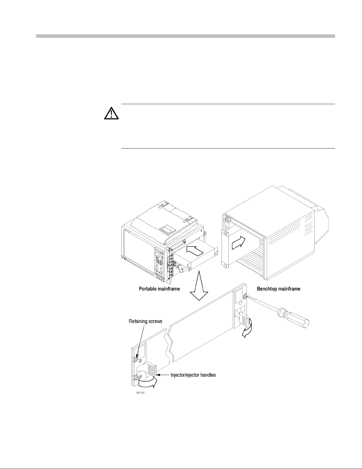
Install Common Hardware
This manual is written assuming that your logic analyzer mainframe is already
installed properly. However, a high-level module installation overview is
provided. If
TLA7000 Series Logic Analyzers Installation Manual.
CAUTION. To avoid damaging the mainframe, do not install or remove any
modules while the mainframe is powered on. Always power off the instrument
before installing or removing modules.
Cover any empty module slots with a blank cover (Tektronix part number,
333-4206-xx).
Install the modules in the mainframe. (See Figure 7.) Use a screwdriver to tighten
the retaining screws to 2.5 in-lbs after seating the modules in place.
you need additional help installing your mainframe, refer to the
Figure 7: Installing a module
Tektronix Logic Protocol Analyzer Solutions for PCI Express 3.0 Instruction Manual 13
Page 36

Connecting the Instrument to the SUT
Connecting th
e Instrument to the SUT
The probes co
following illustration shows possible connections to your SUT. Choose the
probing scheme that works for your application.
nnect your logic protocol analyzer module to the SUT. The
Figure 8: Installation overview
14 Tektronix Logic Protocol Analyzer Solutions for PCI Express 3.0 Instruction Manual
Page 37

Connecting the Instrument to the SUT
The following t
ables list the number of probes needed per module to connect to a
link. Refer to the previous illustration for an overview of the connections to the
logic analyzer and SUT. (See Figure 8 on page 14.)
Additional probe connection information is provided later in this document; refer
to those sections for additional information.
Table 11: TLA Modules and midbus probes per link
Link TLA M od ules Probes
x16
x8
x4, x2, or
x1
Table 12
Link TLA Modu
x16
x8
x4, or x2
x1
2 TLA7SA16 2 P67SA16
1 TLA7SA16 1 P67SA16
1 TLA7SA16 or 1 TLA7SA08 1 P67SA16 or P67SA08
: TLA Modules and slot interposer probes per link
les
2 TLA7SA
1 TLA7S
1 TLA7
1 TLA7
16
A16
SA16 or 1 TLA7SA08
SA16 or 1 TLA7SA08
Probes
1 P67SA1
1 P67SA
A04S
1 P67S
A01S
1 P67S
08S
6S
Table 13: TLA Modules and solder down probes per link
Link TLA M od ules Probes
x16
x8
x4
x1
2TLA7SA16 32 P67SA01SD
1 TLA7SA16 16 P67SA01SD
1 TLA7SA16 or 1 TLA7SA08 8 P67SA01SD
1 TLA7SA16 or 1 TLA7SA08 2 P67SA01SD
Tektronix Logic Protocol Analyzer Solutions for PCI Express 3.0 Instruction Manual 15
Page 38

Connecting the Instrument to the SUT
Clock Cable
Two clock connection cables are included with your logic protocol analyzer
module. One is for connecting the reference clock input of the module to the
SUT or slot in
module to another.
terposer probe, and the other is a jumper cable for connecting one
Connecting a Cloc k Cable
Connecting a Clock
Jumper Cable
Figure 9
Connect a clock cable by following these steps:
1. Connect one end of the cable to the Ref Clock input connectors (+ and –) on
2. Connect the other end of the correct cable to the SUT three-pin connector or
1. Connect one end of the cable to the Ref Clock input connectors (+ and –) on
2. Connect the other end of the cable to the Ref Clock output connectors
NOTE. Clock Reference Source must be set to SUT if either clock cable is used.
(See page 36, Selecting a Clock Signal Source.)
: Clock cable and clock jumper cable
the logic protocol analyzer module; screw the SMA connectors down until
re snug.
they a
lot interposer probe three-pin connector.
the s
the logic protocol analyzer module; screw the SMA connectors down until
yaresnug.
the
and–)onanothermodule.
(+
16 Tektronix Logic Protocol Analyzer Solutions for PCI Express 3.0 Instruction Manual
Page 39

Connecting the Instrument to the SUT
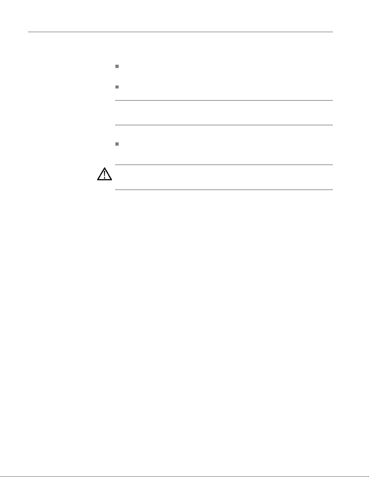
Connecting a P
robe to the Logic Protocol Analyzer Module
Follow these steps to connect a probe to the logic protocol analyzer:
1. Note the label on the module-end of the probe connector and connect the
2. Connect the probe power connector to one of the power connectors on logic
3. Tighten the connector screws using the adjustment tool included with your
Connect the Midbus Probe
The P67S
TLA7SA08 and TLA7SA16 Logic Protocol Analyzer modules to capture PCIe3,
PCIe2, and PCIe1 data from PCIe3 footprints. The P67SA16G2 x8 midbus probes
are designed to connect the TLA7SA08 and TLA7SA16 Logic Protocol Analyzer
modules to signals using PCIe2 footprints. The general probe connection
procedures are the same for all the midbus probes; however the P67SA16G2
x8 mi
probe to the appropriate connector on the logic protocol analyzer (for example
connect the probe with the A connector label to the A connector on the logic
protocol an
protocol a
probe.
dbus probes require a different type of retention m echanism.
alyzer).
nalyzer.
A08 and P67SA16 midbus probes are designed for use w ith the
Connect the midbus probe from the logic protocol analyzer to a retention
hanism on your circuit board. Instructions for installing a retention
mec
mechanism are provided in Appendix B. (See page 123, Installing the Midbus
Retention Mechanism.)
Tektronix Logic Protocol Analyzer Solutions for PCI Express 3.0 Instruction Manual 17
Page 40
Connecting the Instrument to the SUT
Handling the Probe Head
Handle the prob
Handle the probe head by the outer casing. Do not touch the contacts in the
center with fin
Do not expose the connector to liquids or dry chemicals.
NOTE. Be car
connected to a powered module. The probe head may become warm to the touch;
the probe is operating normally.
When connecting the probe, be careful not to touch the probe head contacts to
any other surfaces or components on your circuit board.
CAUTION. Static discharge can damage the probe head. Always wear a grounded
antistatic wrist strap whenever handling the probe head. Also verify that anything
to which the probe head is connected does not carry a static charge.
e head with care. Keep the following points in mind:
gers, tools, wipes, or any other devices.
eful when handling the probe head while the midbus probe is
18 Tektronix Logic Protocol Analyzer Solutions for PCI Express 3.0 Instruction Manual
Page 41
Connecting the Instrument to the SUT
Connect the Probe
Follow these st
your circuit board:
1. Locate the cor
your PCB has multiple retention mechanisms. Be careful to select the correct
one.
2. Align the probe h ead with the retention mechanism. Both are keyed so that
the probe can only be inserted one way.
3. Press the probe head into the retention mechanism.
eps to connect a midbus probe to the retention mechanism on
rect retention m echanism. If you intend to use multiple probes,
Figure 10: Connecting a probe to the retention mechanism
4. Startbothmountingscrewsintheposts, and tighten them evenly to ensure
that the probe approaches and mates squarely to the PCB. Use the adjustment
tool included with your probe. Proper installation torque is 1 in-lb.
Tektronix Logic Protocol Analyzer Solutions for PCI Express 3.0 Instruction Manual 19
Page 42
Connecting the Instrument to the SUT
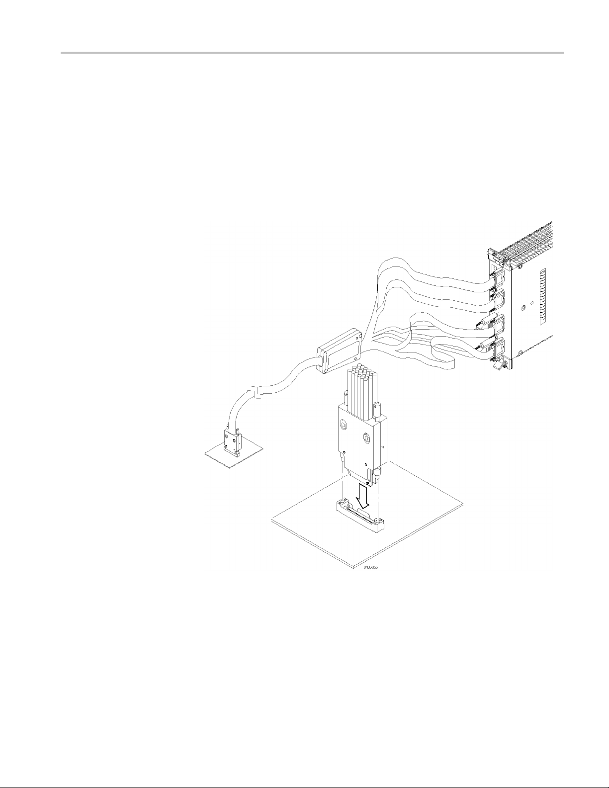
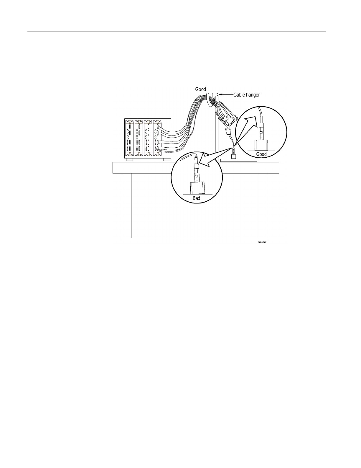
Arranging the Midbus
Probe Cables
Hang the probe c
and tension on the retention mechanism is minimized. Route the cables as straight
as possible, maximizing the bend radius, and making sure that a 90 degree bend
does not occur within three inches of the circuit board surface. (See Figure 11.)
ables so that the probe head is perpendicular to the circuit board,
Figure 11: Arranging the midbus probe cables
20 Tektronix Logic Protocol Analyzer Solutions for PCI Express 3.0 Instruction Manual
Page 43

Connecting the Instrument to the SUT
Connect the Sl
ot Interposer Probe
Handling the Probe Head
Connect the Probe
Connect the slot interposer probe to a PCI Express slot on your SUT.
Handle the probe head with care. Keep the following points in mind:
Handle the probe head by the outer casing. Do not touch the contacts with
fingers, tools, wipes, or any other devices.
Do not expose the connector to liquids or dry chemicals.
When connecting the probe, be careful not to touch the probe head contacts to
any other surfaces or components on your circuit board.
CAUTION. Static discharge can damage the probe head. Always wear a grounded
antistatic wrist strap whenever handling the probe head. Also verify that anything
to which the probe head is connected does not carry a static charge.
Connect a slot interposer probe to a PCI Express slot on your SUT by following
these steps:
NOTE. Although you do not need to power off the TLA before connecting the slot
probe to the SUT, Tektronix recommends that you DO NOT connect the probe
power to the TLA until after making all other connections.
1. Disconnect the power supply to your SUT. Disconnect the PC power supply if
your SUT is connected to one.
NOTE. To provide additional mechanical support for the PCI Express c ard w hen it
connected to the slot probe, install the slot probe bracket. (See page 24, Installing
the Slot SUT Card Support Bracket.)
2. Locate the correct PCI Express slot.
3. Remove the PCI Express card that is in the PCI Express slot of the SUT.
4. Align the probe with the slot.
5. Press the probe head into the slot.
NOTE. Remove the slot probe bracket if it interferes with the add-in PCI Express
card.
6. Insert the PCI Express card into the connect at the top of the slot probe.
Tektronix Logic Protocol Analyzer Solutions for PCI Express 3.0 Instruction Manual 21
Page 44

Connecting the Instrument to the SUT
7. Position the mo
8. Press your PCI Express card device into the probe.
unting bracket and attach the screws.
Figure 12: Connecting a slot interposer probe
NOTE. When the slot interposer is installed, connect the power connector to the
module. The module must be powered on whenever the SUT is powered on for the
PCI Express signals to reach the PCI Express card connected to the probe.
22 Tektronix Logic Protocol Analyzer Solutions for PCI Express 3.0 Instruction Manual
Page 45
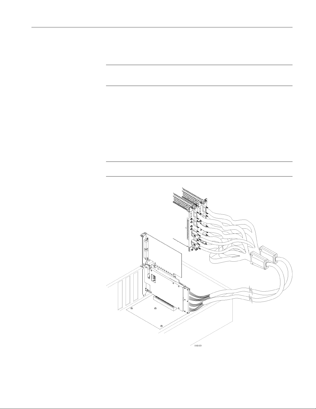
Connecting the Instrument to the SUT
Connecting a Probe to a
x16 Link
To ca pture sign
slot interposer probe. Connect the probe by following these steps:
NOTE. To provide additional mechanical support for the PCI Express c ard w hen it
connected to the slot probe, install the slot probe bracket. (See page 24, Installing
the Slot SUT Card Support Bracket.)
1. Disconnect the power supply to your SUT. If your SUT is connected to a PC
power supp
2. Locate the correct PCI Express slot.
3. Remove the PCI Express card that is in the PCI Express slot of the SUT.
4. Align the probe with the slot.
5. Press the probe head into the slot.
NOTE. Remove the slot probe bracket if it interferes with the add-in PCI Express
card.
als from a x16 link you need to connect two modules to a single
ly, disconnect the power supply.
Tektronix Logic Protocol Analyzer Solutions for PCI Express 3.0 Instruction Manual 23
Page 46
Connecting the Instrument to the SUT
Installing the Slot SUT
Card Support Bracket
6. Position the mo
7. Press your PCI Express card device into the probe.
8. Connect the probe to the two modules and connect the probe power connector
to both modules.
NOTE. The x1
connector to each module. The modules must be powered on whenever the SUT is
powered on for the PCI Express signals to reach the PCI Express card connected
to the probe.
Use the slot SUT card support bracket to provide additional mechanical support
for your PCI Express card when connecting to the slot probe. The following
orientations are available; use the orientation that meets your needs. (See
Figure 13 on page 25.) The illustration shows the support bracket connected to a
x16 slot probe; connections to the x8, x4, and x1 probes are similar.
Install the support bracket parallel with the existing PCI Express bracket
(Option A).
Install the support bracket parallel with the existing PCI Express bracket
in an adjacent card s lot (Option B).
unting bracket and attach the screws.
6 slot probe has two power connectors. Connect one power
Install the support bracket perpendicular to the existing PCI Express bracket
(Option C).
Use either the supplied screws or existing screws to connect the support bracket
to the slot probe.
24 Tektronix Logic Protocol Analyzer Solutions for PCI Express 3.0 Instruction Manual
Page 47
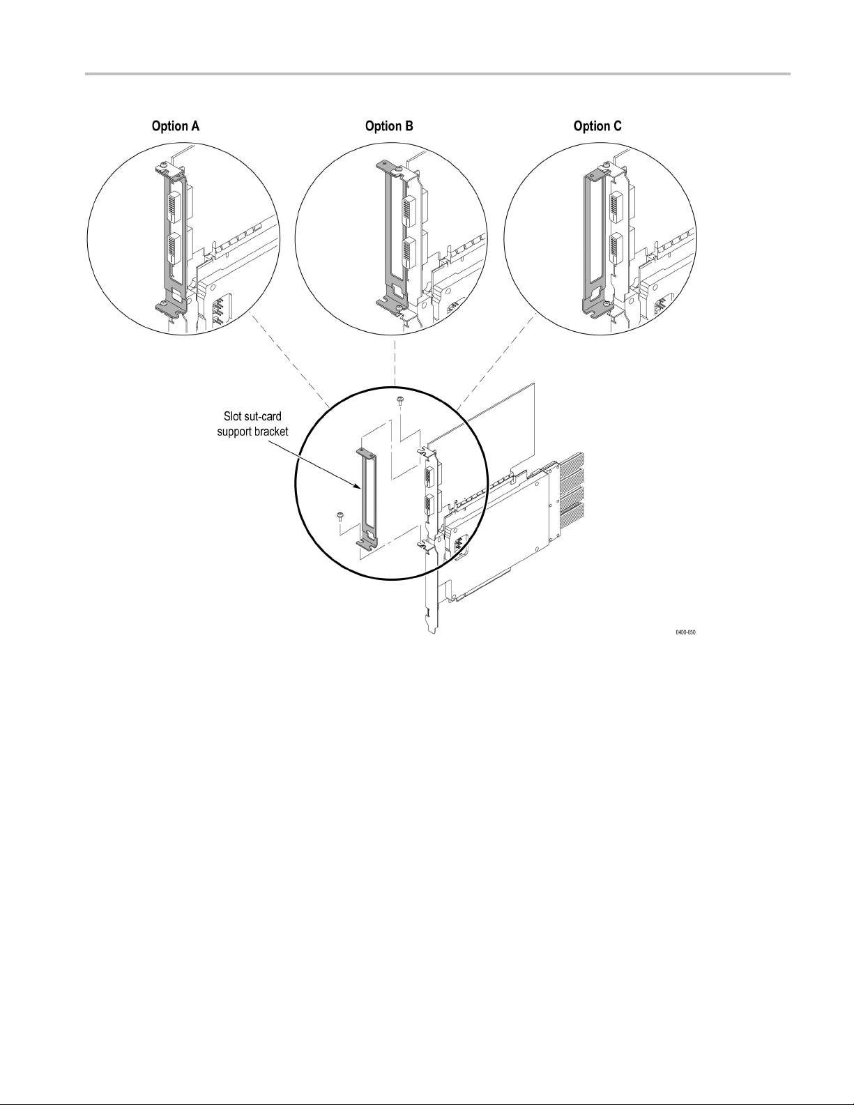
Connecting the Instrument to the SUT
Figure 13: Slot SUT card support bracket configurations
Tektronix Logic Protocol Analyzer Solutions for PCI Express 3.0 Instruction Manual 25
Page 48

Connecting the Instrument to the SUT
Connect the So
Connect to th
lder Down Probe
e Logic
Protocol Analyzer Module
The probe connects to the module and to the probe tip, and the probe tip is
soldered to the circuit. Install the probe by following these steps.
1. Plug the signal connector into the module and tighten the hold-down screws.
2. Plug the probe power adapter into the module and tighten the hold-down
screws.
NOTE. The probe power adapter can be ordered as an option for the solder-down
probe (P67SA01SD Option IP). (See Table 8 on page 11.)
3. Plug the power connector into any one of the receptacles on the Power
Adapter.
4. Plug the solder tip into the solder-down probe.
26 Tektronix Logic Protocol Analyzer Solutions for PCI Express 3.0 Instruction Manual
Page 49

Connecting the Instrument to the SUT
Figure 14: Installing the P67SA01SD probe
P75TLRST Solder Tip
Install the probe tip by following these steps:
NOTE. This tip is very small and must be handled carefully. The following
procedures describe the proper techniques for using the tip.
Connect to the Probe Head. The probe body and tip cable ends are keyed to
ensure correct installation.
1. Orient the probe body with the + and – inputs on top.
2. Align the tip cable lead with the red band to the + input.
Tektronix Logic Protocol Analyzer Solutions for PCI Express 3.0 Instruction Manual 27
Page 50

Connecting the Instrument to the SUT
Figure 15: Connecting the P75TLRST tip to the probe head
3. Hold the cable connector by hand and push the cable into the probe body
until you feel a click. The cable housing is fully seated when it is flush with
theedgeo
4. To remove the tip, pull the cable tab straight out from the probe body.
f the probe body.
CAUTION
the probe. To avoid this, pull only on the cable tab when removing the tip.
Connec
in this manual for reference. (See Figure 46 on page 68.) Design the tip footprint
into your circuit board layout for easier test connections.
To connect the probe tip to your circuit, use the wire and solder that are provided
in the wire replacement kit. The kit includes:
1. Identify a location where the tip can be placed, soldered, and attached to
2. Lay the wires against a circuit board pad, trace, or other conductive feature.
3. Solder the wires to your circuit.
. Pulling the cables when removing the probe tip can damage the tip or
t to the Circuit. The dimensions of the solder tip connections are provided
0.004 in (0.1016 mm) wire
08 in (0.2032 mm) wire
0.0
SAC305 solder (RoHS compliant)
your circuit. When working with long wires (~1 inch), keep the finished wire
ngths of the signal and ground connections as short as possible.
le
If vias or through-holes are very close, thread the wires through them.)
(
28 Tektronix Logic Protocol Analyzer Solutions for PCI Express 3.0 Instruction Manual
Page 51

Connecting the Instrument to the SUT
Figure 16
4. Attach t
5. Clean out the tip vias with a solder-wick material if you are reusing the tip.
6. Press the tip to the circuit board and quickly solder the wires to the tip. Keep
7. Clip off the excess wire from all of the solder joints.
8. Push the end of the tip into the probe head until it seats in the probe head.
: Connecting wires to the circuit
ip tape to the bottom of the tip.
Thread
all fin
the wires through the tip.
ished wire lengths as short as possible.
Tektronix Logic Protocol Analyzer Solutions for PCI Express 3.0 Instruction Manual 29
Page 52

Connecting the Instrument to the SUT
Figure 17: Connecting the tip to the circuit
9. Secure the probe to the circuit board with tape or with the hook-and-loop
strips and dots that are included with the probe.
Applying and Removing Power
After you have connected all probes to the SUT, you are ready to apply power to
the SUT and the logic protocol analyzer.
NOTE. When using slot interposer probes power on the logic protocol analyzer
ore applying power to the SUT.
bef
30 Tektronix Logic Protocol Analyzer Solutions for PCI Express 3.0 Instruction Manual
Page 53

Install the TMS160PCIe3 Support Software
Install the TM
S160PCIe3 Support Software
NOTE. Before you use the logic protocol analyzer, verify that your mainframe
has the most current TLA Application software and the TMS160PCIe3 Support
Software. The TLA Application software must be installed on all mainframes and
PCs that will use the logic p rotocol analyzer modules, including any PCs that will
remotely control the logic protocol analyzer. (See page 117, TLA Application
Software.
To use the TMS160PCIe3 Support Software, install the following CDs:
Follow these steps to install the software:
1. Insert the TMS160PCIe3 Support Software CD in the media drive.
2. Start Windows Explorer, navigate to the media drive and execute the file
3. Click Yes to start the installation and follow the on-screen instructions. If you
)
TMS160PCIe3 Support Software CD, Tektronix part number 063-4236-xx.
TMS160xxxx TLA Add-On Data Windows Software CD, Tektronix part
number 063-4326-xx.
TMS160PCIE3_Setup.exe.
are asked for permission to overwrite any read-only files, select Ye s to A l l.
4. Remove the TMS160PCIe3 Support Software CD from the media drive and
insert the TMS160xxxx TLA Add-On Data Windows Software CD.
5. Using Windows Explorer, navigate to the media drive and execute the file
TMS160View_Setup.exe.
6. Follow the on-screen instructions to install the software.
emove the CD when the installation is complete.
7.R
8. After you start the TLA and connect to the mainframe, a message might
appear instructing you to update the module firmware. If so, update the
module firmware before continuing. (See page 117, Updating the Lo gic
Protocol Analyzer Module Firmware.)
Tektronix Logic Protocol Analyzer Solutions for PCI Express 3.0 Instruction Manual 31
Page 54

Install the TMS160PCIe3 Support Software
32 Tektronix Logic Protocol Analyzer Solutions for PCI Express 3.0 Instruction Manual
Page 55

Using the Logic Protocol Analyzer Software
This section describes how to set up the logic protocol analyzer Setup window
and Trigger window to prepare to acquire data.
Logic Protocol Analyzer Setup Window
The Setup window provides easy access to a variety of configuration options to
do the foll
owing:
Acquire bidirectional data.
Specify the link width and transfer rate.
Useaclockembeddedinthedatastream or use an external clock connected
to the front panel.
Establish storage conditions such as hardware fi ltering, link scrambling and
deskewing, specifying the storage length, and specifying the trigger position.
Establish which modules are associated to links, and perform probe
calibration.
Open t
he Setup Window
NOTE. The instrument has a separate Setup window for each installed module.
Make sure to select the Setup window that applies to the correct module.
Ope
n the Setup window by doing one of the following:
ClicktheSetupIconintheTLAExplorer.
By default the first logic protocol analyzer is identified as SA 1.
Click the Setup button in the System Navigation toolbar.
If your system has more than one module, select the appropriate module from
the Setup button.
Click the Setup button on the Logic Protocol Analyzer icon in the System
window.
Click Setup: SA 1 in the Window menu.
Tektronix Logic Protocol Analyzer Solutions for PCI Express 3.0 Instruction Manual 33
Page 56

Using the Logic Protocol Analyzer Software
The default Set
status indicators near the center of the window will vary depending on the signal
activity at the probe tip.
up window is shown below. (See Figure 18.) The color of the
Figure 18: Default Setup window
34 Tektronix Logic Protocol Analyzer Solutions for PCI Express 3.0 Instruction Manual
Page 57

Using the Logic Protocol Analyzer Software
Monitoring Si
gnal Activity
After you have connected the probes and installed the software and firmware,
monitor signal activity on each of the lanes to make sure that your system
is operating
representation of the logic protocol analyzer module shows a status indicator
for each lane. Use the status indicators to determine if the SUT produces the
signals that the module can recognize. The logic protocol analyzer is constantly
monitoring the status of each lane, even when data is not being acquired. The
status of each lane is mirrored by the front-panel LEDs.
A description of each status indicator is listed below.
Table 14: Status indicators in the Setup window
Indicator Description
correctly and that the probes are connected properly. A graphic
No signal (gray). A signal has not been assigned to a lane.
(See page 37, Assigning Lanes.)
Signal missing. The signal is assigned to a lane, but it is not
recognized. This symbol appears when a lane is inactive.
Signal (yellow). A signal is detected, but data is not
recognized.
Data signal (green). A signal is detected and recognized as
data.
Clock signal. A clock signal is detected via the clock cable
connected to the SUT or slot interposer probe. The colors
and patterns of the clock signal indicator function similar to
those of the other status indicators. This indicator is gray if
the SUT Reference Clock selection is set to Not Used. (See
page 36, Selecting a Clock Signal Source.)
Tektronix Logic Protocol Analyzer Solutions for PCI Express 3.0 Instruction Manual 35
Page 58

Using the Logic Protocol Analyzer Software
Defining the Li
nk
To de fine a link, specify the following information about your SUT; define one
link per module:
Link name. The default link name is Link1. Double-click on the Link tab to
enter a meaningful name.
Acquire. Select one of the Acquire buttons to identify the upstream and
downstream lanes for capturing data. The selection that you make impacts the
appearance of the lane assignments on the right side of the Setup window. For
example, if you select downstream data, the upstream lane assignments become
unavailable.
Switch Sides. Use the Switch Sides button to quickly switch the lane assignments
between the downstream and upstream sides.
Maximum Link Width. Specify the maximum number of lanes in your link.
Transfer Rate. Tektronix recommends setting Transfer R ate to Track Training
(default) when analyzing a bus operating at PCI Express Gen3 specifications. The
logic protocol analyzer module recognizes data as the link trains up in speed
from 2.5 GT/s to 5.0 GT/s or 8.0 GT/s.
Selecting a Clock Signal
Source
The logic protocol analyzer can recognize a clock signal from a cable connection
to the SUT (or slot interposer probe), or by recovering the clock signal embedded
in the data.
Recognize the clock signal embedded in the data stream. To use an embedded
clock signal, set the SUT Reference Clock selection to Not Used.Astable
reference signal is generated by the logic protocol analyze
the embedded clock signal. A clock cable connection is not required, since the
logic protocol analyzer recognizes the embedded signal from the probe.
Recognize the clock signal by directly connecting to the SUT with a clock
cable. Tektronix recommends connecting a clock cable to make sure that data
is accurately synchronized with the clock signal. Set the SUT Reference Clock
selection to Connected at Front Panel and then select an a pproximate frequency
for your application. Make sure the reference clock cable is connected correctly.
(See page 16, Connecting a Clock Cable.)
NOTE. If SSC (spread-spectrum clocking) is enabled, and your PCI Express link
uses power management states, you must connect a clock cable to the SUT and
set the reference clock source to Connected at Front Panel to ensure that all
symbols are recognized by the logic protocol analyzer during the transition from a
power management state to the L0 state.
r and synchronizes with
36 Tektronix Logic Protocol Analyzer Solutions for PCI Express 3.0 Instruction Manual
Page 59

Using the Logic Protocol Analyzer Software
Storage Settings
Descramble and Deske w
Defining
aDataFilter
ning Lanes
Assig
Specify the amo
relative to the amount of data stored. A trigger position setting of 0% indicates
that data will be stored after the trigger event occurs. A trigger position setting of
100% indicates that data storage will stop when the trigger event occurs.
The following guidelines provide information when you should select items in the
Link Data Storage area:
Select Descramble to store data in a descrambled format.
Select Sto
operation).
Select St
Select Deskew Lanes to view time-aligned lane data in the listing window.
The Setup window provides a means of filtering data to focus on the data you are
interested in. Select a predefined data filter from the list, or click Define Filter and
select what you want to filter from the data stream. Click OK when you are done.
In the center of the Setup window, the graphic representation of the logic protocol
analyzer module shows the channel-lane connectors (lines drawn between
numbered lanes and channels depending on the number of lanes in use). For
ple if you have a x4 link, then eight lanes will remain unconnected. The
exam
logic protocol analyzer assigns lanes to channels in the Setup window as it senses
the signals at the probe tip. To change the assignments, click and drag the lines so
that the signals are connected to the lanes as your design dictates.
unt of data to store (symbols per lane), and set the trigger position
re as 10b Data to store data in 10b format (a post-processing
ore as 8b Data to store the more conventional 8b data.
A line connects each signal to a lane so that data will be recorded and displayed
properly in the data windows. Unless all connected indicators are green, the logic
protocol analyzer will not be able to identify packet structures correctly.
Tektronix Logic Protocol Analyzer Solutions for PCI Express 3.0 Instruction Manual 37
Page 60
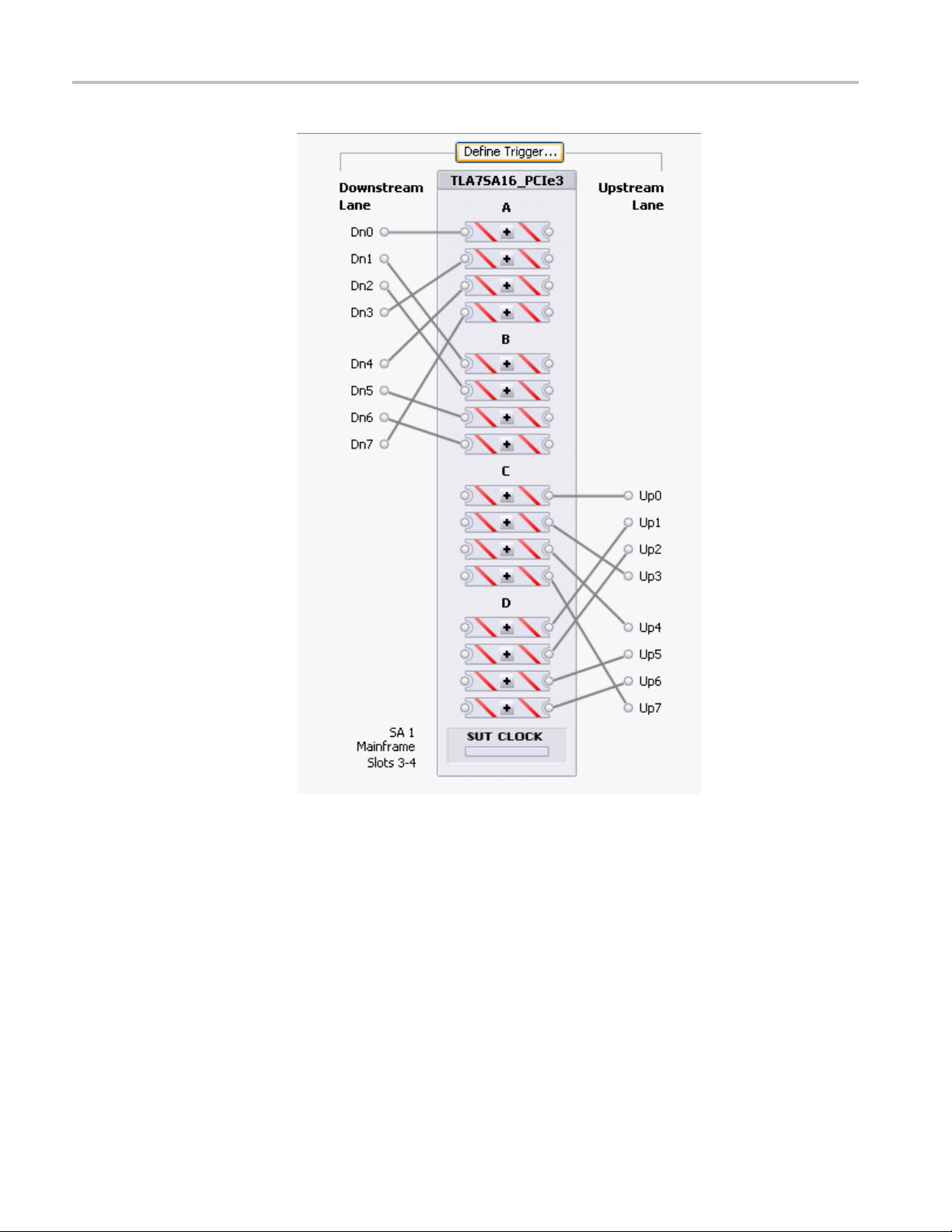
Using the Logic Protocol Analyzer Software
Figure 19: Channel-lane connectors
38 Tektronix Logic Protocol Analyzer Solutions for PCI Express 3.0 Instruction Manual
Page 61
Using the Logic Protocol Analyzer Software
Changing the M
Trigger Window
aximum Electrical Idle Timeout
When the Transfer Rate is set to Track Training and an electrical idle occurs
longer than the specified timeout, the module switches the acquisition rate to
2.5 GT/s. An e
again in 2.5 GT/s mode.
Some applic
The circuits should have returned from an L1 state within the timeout period.
However, some tests might require a longer timeout setting. Adjust the maximum
timeout for your application. To view or set the timeout setting, right-click the
mouse in the Channel-Lane Assignment area of the Setup window and select
Front End Settings. Adjust the timeout setting in the window.
After defining parameters in the Setup window, define a trigger that tells the logic
ol analyzer when to begin recording data. The logic protocol analyzer
protoc
provides powerful triggering capabilities including predefined trigger templates to
specify trigger conditions on any field within a packet.
lectrical idle can happen when the SUT has shut down and starts up
ations return to an electrical idle after a preset timeout period.
Open the Trigger Window
NOTE. The instrument has a separate Trigger window for each installed module.
Make
Open the Trigger window by doing one of the following:
sure that you select the Trigger window that applies to your module.
Click the Trigger icon in the TLA Explorer.
By default the first logic protocol analyzer is identified as SA 1.
Select the Logic Protocol Analyzer from the Trigger button in the TLA toolbar.
Click the Trigger button on the Logic Protocol Analyzer icon in the System
window.
Click Trigger: SA 1 in the Window menu.
Click Define Trigger in the Setup window.
Tektronix Logic Protocol Analyzer Solutions for PCI Express 3.0 Instruction Manual 39
Page 62

Using the Logic Protocol Analyzer Software
Quick Tips
The default Tri
Figure 20: Default Trigger window
Click to collapse the current trigger state to provide more room on the
screen.
gger window is shown below. (See Figure 20.)
Adding States, Clauses,
Events, and Actions
Click to
Look fo
They are indicators that there may be more or less information to display
on screen.
Click one of the three icons at the top of the Trigger window to open the
default trigger window
The Store and Trigger Position controls are identical to those in the Setup
window.
A trigger definition is a logical expression consisting of events and actions within
clauses, within states. The default Trigger window starts with one state (State 1).
and one clause (Clause 1). A trigger definition can have up to eight trigger states
with eight trigger clauses per state. To work with states, clauses, events, and
actions, do the following:
1. Begin editing the clause by selecting Events (IF) and Actions (THEN).
2. To add additional events or actions to the clause, click Add Event or Add
Action.
3. Multiple events can be joined by a logical AND or an OR. Click AND to
changeittoanOR.ActionscanonlybejoinedbyanAND.
expand the current trigger state.
rthe
or to expand or collapse information in the current Clause.
, load a trigger , or save a trigger .
40 Tektronix Logic Protocol Analyzer Solutions for PCI Express 3.0 Instruction Manual
Page 63

Using the Logic Protocol Analyzer Software
Deleting States, Clauses,
Events, and Actions
Trigger Events
4. To add another c
lause or state, click Add Clause or Add State.
5. Add states, clauses, events, and actions by right-clicking and selecting from
the context me
nu.
Delete states, clauses, events, and actions by clicking the appropriate button in the
Trigger window, selecting from the Edit menu, or by right-clicking and selecting
from the con
text menu.
Trigger events are listed in the following table.
Table 15: Trigger events
Event D escription
Anything Recognizes any data.
TLP
DLLP
Seque
Link E
Timer
nter
Cou
nal In
Sig
nce
vent
Recognizes the presence or absence of a specificTLP.
Choose the TLP from a list, or defineaTLP.
Recognizes the presence or absence of a specific DLLP.
Choose
Recog
Choose the Sequence from a list, or define a Sequence.
Recognizes link events and link errors. Choose the Link
Event from a list, or define a Link Event and specify which
lane
Reco
Rec
Rec
the DLLP from a list, or defineaDLLP.
nizes a specific ordered set or symbol sequence.
s to monitor.
gnizes a specified timer value.
ognizes a specified counter value.
ognizes a signal from another module.
The following table provides additional information about the event recognizer
resources. You may need to be aware of these when setting up the Trigger window.
Table 16: Trigger event recognizer resources
Event recognizer Description
DLLP packet recognizers 4 per link direction
TLP packet recognizers 4 per link direction
Symbol sequence recognizers
Link event recognizers 4 per link direction
4 shared between link directions
Tektronix Logic Protocol Analyzer Solutions for PCI Express 3.0 Instruction Manual 41
Page 64

Using the Logic Protocol Analyzer Software
TLP. Select TLP
Figure 21: Specifying a TLP event
Click the ellipsis to define a more detailed TLP.
Figure 2
2: Defining a TLP
from the list and specify your TLP.
Enter a
be created. To change the radix, right-click and select from the list. Edit the
TLP definition and click Close when you are finished. The new TLP will now
appear in the list.
meaningful name for the TLP or select one from the list and a copy will
42 Tektronix Logic Protocol Analyzer Solutions for PCI Express 3.0 Instruction Manual
Page 65

Using the Logic Protocol Analyzer Software
DLLP. Select DL
Figure 23: Specifying a DLLP event
Click the ellipsis to defineamoredetailedDLLP.
Figure 24: Defining a DLLP
LP from the list and specify your DLLP.
Enter a meaningful name for the DLLP or select one from the list and a copy will
ated. To change the radix, right-click and select from the list. Edit the
be cre
DLLP definition and click Close when you are done. The new DLLP will now
appear in the list.
Tektronix Logic Protocol Analyzer Solutions for PCI Express 3.0 Instruction Manual 43
Page 66

Using the Logic Protocol Analyzer Software
Link Event. Sel
Figure 25: Specifying a Link event
Click the ellipsis to define a more detailed Link event.
ect Link Event from the list and specify your Link event.
Figure 26: Defining a Link event
Enter a meaningful name for the Link event o r select one from the list and a copy
will be created. Edit the Link event definition and click Close when you are done.
new event will now appear in the list.
The
44 Tektronix Logic Protocol Analyzer Solutions for PCI Express 3.0 Instruction Manual
Page 67

Using the Logic Protocol Analyzer Software
Sequence. Sele
ordered set.
Figure 27: Specifying a symbol sequence
Click the ellipsis to define a more detailed symbol sequence.
ct Sequence from the list and specify your symbol sequence or
Figure 28: Defining a symbol sequence
Enter a meaningful name for the symbol sequence or select one from the list and a
y will be created. Define a symbol sequence with a maximum of 16 symbols
cop
per lane. Click the K to change it to a D or an X. An X indicates that the trigger
will recognize either a K or a D control bit. To change the radix, right-click
and select from the list, or just click the radix text. Edit the symbol sequence
definition and click Close when you are done. The new symbol sequence will
now appear in the list.
Tektronix Logic Protocol Analyzer Solutions for PCI Express 3.0 Instruction Manual 45
Page 68

Using the Logic Protocol Analyzer Software
Event Counters
associated with them. The counter will increment every time the event occurs (or
does not occur). These counters are called event counters and are associated with
the following events:
TLP
DLLP
Sequence
Link Event
Figure 29: Event counter
There are two event counters in every state. Event counters are limited to
counting only the event they are associated with. To create a counter that can be
incremented, decremented, and reset by any clause in any state, select Counter
from the event list. This type of counter is called a global counter.
, Global Counters, and Timers. Four types of events have counters
There are four counter/timers that may be used as either Global Counters, or
Global Timers. A counter/timer can not be used
Global Timer in the same trigger program. Each individual counter timers are
independently enabled to be a Global Counter or a Global Timer.
Figure 30: Specifying a global counter
Global counters are usually combined with another clause or state that increments,
decrements, or resets the counter with an action. See Actions.
Timers are also global, meaning that t hey can be started, stopped and reset by any
clause in any state. Select Timer from the event list and specify your timer.
Figure 31: Specifying a timer
Timers are usually combined with another clause or state that starts, stops, or
resets the timer with an action. See Actions. A maximum of four global counters
or timers are available.
as both a Global Counter and a
46 Tektronix Logic Protocol Analyzer Solutions for PCI Express 3.0 Instruction Manual
Page 69

Using the Logic Protocol Analyzer Software
Signal In. Sele
ct Signal In from the event list and specify a signal number.
There are four global signals that can be used for triggering by any module
he logic analyzer mainframe.
Trigger Actions
installed in t
When an event (IF) in a clause becomes TRUE, the associated action (THEN) is
taken. Click Add Action to join multiple actions with a logical AND.
Trigger Actions are listed in the following table.
Table 17: Trigger actions
Action Description Interactions
Trigger Triggers the current module and causes
acquisition memory postfi ll to begin.
Trigger All Modules
Wait for System Trigger Used for a module that does not trigger
Go To Causes a change to a different trigger
Counter actions
Timer actions
Set and Clear Signal Sets or clears one of the four internal
Arm M odule
Start and Stop Storing Begins or ends storing of samples.
Do Nothing
Also known as a System trigger. This
signal is also available at the System
Trigger Out connector.
itself or any other module, but waits to be
triggered by another module.
state.
Increments, decrements, or resets
counters.
Starts, stops, or resets timers. Counter 1, 2, 3, and 4 actions conflict with
system signals.
Sends an Arm signal to another module.
The other module begins running its
trigger program.
Used as a placeholder when defining a
complicated trigger program.
When Trigger is used in the trigger
program, Trigger All Modules cannot be
used.
When Trigger All Modules is used in the
trigger program, Trigger cannot be used.
Capable of receiving the following three
(mutually exclusive) trigger actions:
Trigger, Trigger all Modules, or Wait for
System Trigger.
Use only one in clause definition.
Counter 1, 2, 3, and 4 actions conflict with
Timer 1, 2, 3, and 4 actions respectively.
The actions also conflict with their
respective events.
Timer 1, 2, 3, and 4 actions respectively.
The actions also conflict with their
respective events.
Use only one in a trigger program.
Mutually exclusive with Arm Module
action.
Can only arm one module in a trigger
program, but actions can be taken
throughout the trigger program.
Does not override other actions specified
in a clause.
Tektronix Logic Protocol Analyzer Solutions for PCI Express 3.0 Instruction Manual 47
Page 70

Acquiring and Viewing Data
Acquiring and Viewing D ata
After defining the Setup window and the Trigger window parameters, use one of
the following data windows to view and analyze the data.
NOTE. When y
Waveform window. Use the New Data Window wizard to select and set up other
data windows as needed for your application.
Use the Transaction window to locate transactions of interest and to help
understand the detailed sequence of the transactions. After locating a
transaction of interest, use the Transaction window to further examine the
packet sequence, timing, and internal content to confirm any suspected
problems.
Use the Summary Profile window to view a summary statistical analysis of
protocol elements within a region and across the entire acquisition.
Use the Listing window to display columns of disassembled PCI Express
symbol data (ordered sets, DLLPs, and TLPs). Each column represents a lane
of PCI
you to quickly view symbol data as it flows across the link.
Use t
represents a lane of PCI Express data. Use iView to correlated data from an
external Tektronix oscilloscope in the same waveform window.
ou first acquire data, the logic protocol analyzer displays the
Express data with a disassembled view of the packet data. This allows
he Waveform window to display rows of symbol data. Each row
48 Tektronix Logic Protocol Analyzer Solutions for PCI Express 3.0 Instruction Manual
Page 71

Acquiring and Viewing Data
SettingUpthe
Data Windows
Acquiring D ata
Transaction Window
Opening the Transaction
Window
The TMS160PCIE3 PCI Express Support software provides predefined setups for
the Waveform and Listing windows.
Acquiredataafterdefining the setup parameters. Click the Run button to begin
the data ac
The Trans
by packet type, to view transactions and overall packet flow, interspersed with
physical layer activity (such as ordered sets) to gain an understanding of traffic
flows within your system.
Use the New Data Window wizard to create the Transaction window or other data
windows that you might need for your application.
1. (Click
quisition sequence.
action window provides a display of packet information, colored
in the TLA toolbar or select New Data Window from the TLA
Window menu).
2. Select Transaction in the New Data Window wizard and click OK.
If your TLA system is configured with one or more logic protocol analyzer
modules to acquire one protocol (PCI Express), the Transaction window opens
without needing additional configuration information. Based on the Setup
window information, all such modules are automatically identified as participating
bidirectional links.
If your TLA system is configured to acquire multiple protocols, or if the system
does not detect any protocols in the setup, the Component and Link dialog box
ppears on the screen. Fill out the necessary fields in the dialog box to associate
a
the links captured by the modules to a Transaction window.
NOTE. If there are no logic protocol analyzer modules configured for one of the
supported protocols, the Component and Link dialog box will not accept any
information.
After defining one or more Transaction windows, return to the desired window
by clicking the Transaction window icon in the System window or in the TLA
Explorer. Alternatively select the Transaction window from the Window menu.
Tektronix Logic Protocol Analyzer Solutions for PCI Express 3.0 Instruction Manual 49
Page 72

Acquiring and Viewing Data
Transaction Window
Elements
Figure 32: Transaction window
The following i
window.
The Transaction window has elements similar to other data windows such as the
toolbar where you can search data, apply filters, and manage other aspects of the
display.
llustration shows some of the key elements in the Transaction
Quick Tip
Transaction view. The Transaction view provides a way to quickly navigate trough
transactions in a top-down way. Other than the Timestamp column, each column
in the Transaction view represents the endpoints of a link. The rows display the
Timestamp and transaction initiators (the start of a transaction) as packet names.
Links are represented as relationships between the end point columns.
Click a transaction to show the link relationship by displaying a Feynman
diagram. (See page 51, Examining Transactions.)
Use the mouse with roll-over messages to show the amount of time required for
the transaction or to identify errors in the transaction.
Status area. The status area shows status messages and error messages as they
occur. It includes access to filter check-boxes to quickly turn PCIe elements on
or off. It provides access to the Summary Profile window through the View
Summary button. (See page 53, Summary Profile Window.)
Packet view. The Packet view shows the primary source of information in the
Transaction window. All acquired packets are interleaved in the timestamp
followed by the source (transmitter) ID. Packets come in different sizes and
transmit in varying amounts of time.
50 Tektronix Logic Protocol Analyzer Solutions for PCI Express 3.0 Instruction Manual
Page 73

Acquiring and Viewing Data
Quick Tip
The columns in t
packet. To add or remove columns, right-click the mouse and select Add/Remove
Columns from the context menu; add or delete columns from the Field Chooser
menu.
Each row in the Packet view represents a packet. Click the + sign to expand the
fields to see more packet information.
Coloring provides a way to differentiate packets, such as Memory Reads, Memory
Writes, ACK, NACK, message types.
Bird’s eye view (BEV). The BEV provides the highest acc ess to the acquisition
data. Use the BEV to do the following:
Quickly move to a new location in the acquisition.
Identify the current position in relation to the overall acquisition.
See marks and cursors in relation to the current view.
Move marks and cursors.
Watch the progress of the system as it completes time-sensitive operations.
Reduce the packet rows to a few pixels high to only display the color bands
without the detailed text labels by continuing to select Smaller Text from the
right-click menu. This provides an easy way view more data in the window.
he Packet view show information from the fields available to the
Examining Transactions
Click a transaction to see
packets involved in the transaction are added to the appropriate columns and are
highlighted. Click the transaction a second time to remove the highlighting.
All packets related by the transaction are highlighted and have arrows drawn
from them to their ultimate delivery time; all other packets are attenuated with
grayed-out text. Ends of the arrows indicate when a packet has fully arrived;
position the mouse on the arrow to show amount of time between packets.
NOTE. Because packets do not flow across links instantly, abnormally long or
short transmission times can indicate the source of a problem. Use the timestamp
to indicate when the packet left the sending component.
If the target row does not display (is filtered out) the arrow is drawn to the top
of the nearest visible and appropriate timestamp row. The arrowhead is rendered
with a colored border with a white fill. The last line for the last packet to complete
is shown by a square-end cap; it indicates there are no more packets in the current
transaction.
A vertical line indicates how long the component was involved with the
transaction after it received the first packet.
the packets that make up the transaction. Other
Tektronix Logic Protocol Analyzer Solutions for PCI Express 3.0 Instruction Manual 51
Page 74

Acquiring and Viewing Data
Physical Layer View
Using the Transaction
Window with the Listing
Window
The Packet view
information. Use the Packet view to look for errors and gaps due to hardware
filtering or to identify other problems in the Physical layer. The interleaving
of the physical information with the packet information can help in identifying
elements of interest.
Special events are identified as information events, ordered sets, or error messages.
These events may be displayed as horizontal lines starting in the left side of the
Packet view. Each line has a different appearance; use the rollover messages with
the mouse t
Use the Transaction window and Listing window together to trace problems
from the Transaction window by locking cursor 1 to the same data in the Listing
window.
at the same time.
Position the windows side-by-side to view activity in both windows
shows Physical layer information in addition to the packet
o provide more information about the special events.
Figure 33: Side-by-side Transaction window and Listing window
Lock cursors between data windows to look for problems. For example, look
or problems when the data rate changes from 8 GTs to 5 GTs. There might be
f
problems in the disruption in the packet with the ordered set.
ind a link rate change because of new sets of training information (moving from
F
TS1 to TS2). Look for the relative lane data in the Listing window to identify the
rate change. Then look for additional information in the Listing window to see the
lane data to identify what is going on.
52 Tektronix Logic Protocol Analyzer Solutions for PCI Express 3.0 Instruction Manual
Page 75

Acquiring and Viewing Data
Summary Profil
eWindow
Use the Summary Profile window to view a summary statistical analysis of
protocol elements within a region and across the entire acquisition. The window
provides rea
view the overall health of your system. Summary information includes statistical
analysis of the trace elements such as:
A Summary Profile window is associated with one or more Transaction widows
for any one protocol. To view the Summary Profile window, click the View
Summary button on the status bar of the Transaction w indow.
l-time statistics without the need to take a separate acquisition to
TLPs
DLLPs
Ordered sets
Errors
Custom
Figure 34: Opening the Summary Profile window
Tektronix Logic Protocol Analyzer Solutions for PCI Express 3.0 Instruction Manual 53
Page 76

Acquiring and Viewing Data
Summary
Statistics Tab
Notebook
The following i
window.
Figure 35: Summary Profile window
The Summary Statistics Tab Notebook contains a collection of the summary
statistics. The tabs identify the individual links or copies of the links with an
associated Transaction window instance. Each tab contains a list of protocol
nts and a list of the totals of elements in the viewfinder regions in the
eleme
overall acquisition.
llustration shows the major components of the Summary Profile
54 Tektronix Logic Protocol Analyzer Solutions for PCI Express 3.0 Instruction Manual
Page 77
Acquiring and Viewing Data
Element Table
Figure 36: Summary Profile window (Summary Statistics Tab Notebook)
The Element table contains the following items:
Protocol Element. This column lists the hierarchy of the elements in the
protocol. Click the arrow to display any sub-elements and the details for those
elements. The column may contain filtered items (in italics) that represent
s not displayed in the Transaction window because of post-processing
item
filtering. Click elements with hyperlinks to scroll the associated Transaction
window to the first instance of the element.
The In Viewfinder columns list the totals of each element within the
Viewfinder regions. Click an item a Viewfinder column to scroll to the
first occurrence of the corresponding item in the Transaction window. (See
Figure 36.)
Tektronix Logic Protocol Analyzer Solutions for PCI Express 3.0 Instruction Manual 55
Page 78

Acquiring and Viewing Data
Using the Custom Element
The In Total col
acquisition. Click a n item in the column to scroll to the first occurrence of
the corresponding item in the Transaction window.
The Overview column contains a summary of each element in the acquisition
including the following items:
Viewfinder, a means of specifying an area o f the sparklines that looks
interesting. Changing the viewfinders, updates the statistics under In
Viewfinder columns. Click the updated hyperlink to go to the first instance
on an element in the viewfinder region.
Sparklines, a summary of the entire trace data for each element broken
into segments (approximately 40 discrete sections over the entire trace).
The horizontal (X) dimension is each segment; the vertical (Y) dimension
depends
sparkline is part of.
Use the Custom element to establish user-defined protocol elements for which
the Sum
element does not create a new packet type, but provides a means to specify a set
of values for the fields of a packet that may or may not correspond to an existing
packet definition.
mary Profile window will provide appropriate statistics. The Custom
umn lists the grand totals of each element in the entire
on the maximum value of the element and which root element the
Click the button next to the Custom element to open the Define Packet window.
Select one of the default packet types from the Name list. (See Figure 37.)
Figure 37: Define Packet window for a Custom element in the Summary Profile
window
Enter a name for the packet and then change the values of the fields for your
needs. Save the Custom element by clicking Save. The new element is added
to the Protocol Element list.
56 Tektronix Logic Protocol Analyzer Solutions for PCI Express 3.0 Instruction Manual
Page 79
Acquiring and Viewing Data
Listing Window
Some guideline
s for Custom elements are listed below:
DLLPs start with an SDP and complete with an End or EDB with mod4 lane
starts and a maximum of two SDP per symbol times.
TLPs start with SDP and finish with an End or EDB with mod4 lane starts and
a maximum of one STP per symbol time.
he maximum packet sizes are defined by Max_Payload_Size.
T
Use the Listing window with the Transaction window and Summary Profile
window to display disassembled data in a list format; packets appear in searchable
columns.
Figure 38: Data displayed in the Listing window
The Listing window displays special characters and strings to indicate significant
events. (See Table 18.) The columns that display in the Listing w indow depend
on the Acquire settings in the Setup window.
Table 18: Special characters in the Listing window
Character or string Description
>
--
Insufficient room on the screen to show all available data
Invalid data or group, including read data
Tektronix Logic Protocol Analyzer Solutions for PCI Express 3.0 Instruction Manual 57
Page 80

Acquiring and Viewing Data
Adding two Sides of a Link
to a Single Listing Window
If you are using
upstream side of a link and the other module is connected to the downstream side,
display both sides of the link in a single listing window. To do this, complete
the following steps:
1. Select New Data Window from the Window menu to start the New Data
Window wizard.
2. Click Listing and then Click OK.
3. Press the Ctrl key on your keyboard and select the two modules from the
Data from list.
Both modules should be selected in the wizard.
4. Click Nex
5. Enter a name for the new Listing window and then click Finish.
The wizard will close and display the data from both modules in the new
listing window.
6. If necessary, edit the window by adding or moving columns to display the
data that you are interested in.
two logic protocol analyzer modules and one is connected to the
t>.
Changing How Data is Displayed
The logic protocol analyzer provides different ways for viewing data in Listing
aveform windows. Change the display settings in the properties pages of
and W
either display window:
1. Click the Properties icon
pages for the respective display.
2. Click the Disassembly tab to select the Disassembly property page.
3. Change the display items as needed.
he following table lists some of the display settings that you can change in the
T
Listing window.
in either display window to open the property
58 Tektronix Logic Protocol Analyzer Solutions for PCI Express 3.0 Instruction Manual
Page 81

Acquiring and Viewing Data
Table 19: Logic
Disassembly p
page selections Settings D escription
Show
Highlight
mble Across Gaps
Disasse
protocol analyzer disassembly display options
roperty
All (default)
Non-Idle Sam
TLP/DLLPs O
TLPs Only Only samples containing
TLP Headers Only Only samples containing
None (de
Yes or No
ples
nly
fault)
(default)
All required d
disassembled and shown
including logical idle
samples
Logical idle samples are
hidden
Only sample
TLPs and DLLPs are shown
TLPs are shown
TLP heade
Nothing is highlighted
General
setting. (not recommended
for PCI Express data)
ata i s
s containing
rs are shown
listing window
Any errors in link traffic detected by the disassembler are displayed regardless of
the display option that you selected.
Bus-Specific Fields
In the Controls area of the Disassembly property page, select any of the following
controls to change the way data is displayed.
Disassemble and Display. When working with bidirectional data with a single
module, the data window can only disassemble and display either upstre am or
downstream data. Select the data that you want to view in the Listing window.
Extended Link Details. Set the Extended Link Details mode to ON or OFF to show
or hide extended packet information in the Listing window. If you set it to OFF,
the Link_Details column displa
ys general p acket information on a single line. If
you set it to ON, the Link_Details column displays extended packet information
on multiple lines. All packet fields are decoded and displayed in the Link_Details
column. TLP payload data is displayed double word aligned along with the lower
word address starting with the address acquired in the TLP header.
Calculate CRC. The disassembler calculates the CRCs for all packets when
Calculate CRS is set to ON. If the calculated value differs from the value acquired
from the link, an error message is displayed in the Link_Details column. The
default setting is OFF.
By default, the field values are aligned w ith the sample containing the STP if it
is a TLP, or with the sample containing the SDP if it is a DLLP. By setting this
property to ON, the packet field values are displayed on the same line as the
TLP_fmttype and DLLP_type group values.
Tektronix Logic Protocol Analyzer Solutions for PCI Express 3.0 Instruction Manual 59
Page 82

Acquiring and Viewing Data
10-Bit Mode Acquisition
When the logic p
the Listing window displays the symbol encoding in the individual lane columns.
No further link analysis is performed.
Changing from Binary
Listing Symbol Tables to
10-Bit Mode
To change the
acquisition, select a column and right-click the mouse. Select Radix and then
Symbolic. Select one of the symbol files from the list, or click Other and navigate
to the location of the symbol file.
Special Messages
The disassembler uses special messages to indicate significant events. These
messages are highlighted in red in the Link Details column of the listing window.
The following tables list the messages and their descriptions.
The special messages are in addition to the errors detected by the logic protocol
analyzer hardware listed in the PCIEx_RuleViol.tsf file. The file is located in
the C:\
Uni_Dn subfolders.
Table 20: Training sequence messages
rotocol analyzer is configuredtoacquirethelinkin10-bitmode,
radix of a binary listing symbol table to radix in 10-bit mode
Program Files\TLA 700\\Serial\PCIe folder under the Bidir, Uni_Up, or
Message Description
- Duplicate Lane Number
Error
Assignment in Lanes:
r - Lanes That Exceed Maximum Link
Erro
Width:
Lane??: Lane Polarity In The lane is inverted. Click the center of the polarity indicator (+ or -) in the graphical
han one lane is assigned the lane number. The lane numbers are listed below
More t
the message.
ane number as acquired in the training sequence is higher than the link width. The
The l
lane numbers are listed below the message.
display in the Setup window to fix the polarity problem.
Table 21: Packet framing messages
Message Description
Error: Abnormal packet termination The packet was interrupted and terminated by a skip ordered set, training sequence,
or FTS, TLP, DLLP.
Non-Idle Bus
able 22: DLLP messages
T
essage
M
Error reading DLLP A general error occurred while trying to decode the DLLP. This was possibly caused
The link is supposed to be in logical idle at this sample, but a nonzero value is found in
one or more lanes.
escription
D
by a gap/suppression of data.
60 Tektronix Logic Protocol Analyzer Solutions for PCI Express 3.0 Instruction Manual
Page 83

Acquiring and Viewing Data
Table 23: TLP he
Message Description
Error reading TLP A general error occurred while trying to decode the TLP header, possibly caused by a
Error Forwar
Error: Inva
Req TLP
Error: Invalid LastDWBE/Length values
for Req TLP
Zero Length Read Request – Possible
Flush
Error: Invalid Traffic Class for Message
TLP
Complet
Request’, ‘Config Req Rtry Stat’, or
‘Completer Abort’
TLP: Msg - + ‘ERR_COR’,
‘ERR_N
lid 1stDWBE/Length values for
ion Status: + ‘Unsupported
ONFATAL’, or ‘ERR_FATAL’
ader messages
ding/Poisoned TLP
gap/suppress
The EP field of
The TLP leng
The TLP length field is 1 and Last DWBE field is not 0, or TLP length field>1and
Last DWBE field is 0 for request TLPs.
The TLP length field is 1, Last DWBE is 0, First DWBE is 0, for Memory Read Request.
The T C field was not zero.
A comple
An error message TLP was acquired.
ion of data.
TLP header is HIGH.
th field > 1 and First DWBE field is 0 for request TLPs.
tion status other than ‘Successful Completion’.
Table 24: CRC checking messages
Message Description
Error: ECRC mismatch The ECRC value acquired in the TLP digest field does not match the ECRC value
calculated by applying the ECRC algorithm to the acquired data. Possible causes
include incorrect ECRC at the transmitter, poor signal quality at probe head, different
algorithm used between transmitter and software, incorrect polarity or ordering of cables
at the input of the logic protocol analyzer, problem with the cables or connection to the
logic p rotocol analyzer.
Error: CRC mismatch The TLP or DLLP CRC acquired does not match the CRC value calculated by applying
the CRC algorithm to the acquired data.
ble 25: General acquisition messages
Ta
ssage
Me
ror: Missing Data - Gap in TLP header
Er
rror: Missing Data - Gap in DLLP
E
rror: Missing Data - Gap in Training
E
Sequence
Error: Missing Data - Gap in packet Complete decode of Training Sequence ordered set was not possible due to a gap
Lane-to-Lane Deskew Error The link was not properly deskewed by the logic protocol analyzer. Also displayed
scription
De
mplete decode of TLP header was not possible due to a gap or suppression of data
Co
omplete decode of DLLP was not possible due to a gap or suppression of data
C
omplete decode of Training Sequence ordered set was not possible due to a gap
C
or suppression of data
or suppression of data
when the sample contains SKP (K28.0) symbols in one or more lanes but not all lanes
of the link. This error message is displayed until a sample containing all SKP (K28.0)
symbols is found. No further post processing of packets is performed when the link is
not deskewed.
Tektronix Logic Protocol Analyzer Solutions for PCI Express 3.0 Instruction Manual 61
Page 84

Vendor Defined Message (VDM) Support
Vendor Defined
Message (VDM) Support
The TLA7SA08
Defined Message (VDM) support to define and decode vendor-defined packets
and fields. Tektronix provides information about VDM support in a file that you
use to configure the VDM decoder (PacketFormats_VDM.xml).
Modify the decoder file with the VDM information specific to your system.
NOTE. Install the TMS160PCIe3 Support Software on your TLA system to access
the decoder file.
The decoder file is available in the following location on your TLA system:
C:\Program Files\TLA 700\System\CommonAssemblies\
PacketFormats_VDM.xml
and TLA7SA16 Logic Protocol Analyzers provide Vendor
62 Tektronix Logic Protocol Analyzer Solutions for PCI Express 3.0 Instruction Manual
Page 85

Probe Dimensions
The following figure shows dimensions of the P67SA08 and P67SA16 series
midbus probes. Both probes have the same cable lengths. (See Figure 39.)
Figure 39: P67SA08 and P67SA16 cable length dimensions
Tektronix Logic Protocol Analyzer Solutions for PCI Express 3.0 Instruction Manual 63
Page 86
Probe Dimensions
P67SA08 Midbus Probe
Head Dimensions
The following fi
head. (See Figure 40.) A 3D CAD solid model (pcie_gen3_x4_probe.stp file is
attached to the PDF version of this document. (See page 121, Midbus Probe
3D CAD Models.)
NOTE. 3D CAD solid models are included in the electronic files that are attached
to the PDF file of this document. To access the attached files, open the PDF file
and click on the paperclip icon on the lower-left side of the document viewer.
gure shows the dimensions of the P67SA08 series midbus probe
Figure 40: P67SA08 midbus probe head dimensions
64 Tektronix Logic Protocol Analyzer Solutions for PCI Express 3.0 Instruction Manual
Page 87

Probe Dimensions
P67SA16 Midbus Probe
Head Dimensions
The following fi
head. (See Figure 41.) A 3D CAD solid model (pcie_gen3_x8_probe.stp file is
attached to the PDF version of this document. (See page 121, Midbus Probe
3D CAD Models.)
NOTE. 3D CAD solid models are included in the electronic files t hat are attached
to the PDF fi le of this document. To access the attached files, open the PDF file
and click on the paperclip icon on the lower-left side of the document viewer.
gure shows the dimensions of the P67SA16 series midbus probe
Figure 41: P67SA16 midbus probe head dimensions
Tektronix Logic Protocol Analyzer Solutions for PCI Express 3.0 Instruction Manual 65
Page 88

Probe Dimensions
The following fi
probes; all slot probes have the same cable lengths.
Figure 42: P67SA16S, P67SA08S, P67SA04S and P67SA01S Slot Interposer probe
cable lengths
gures show the dimensions of the P67SAxxS Slot Interposer
Figure 43: P67SA16S Slot Interposer Probe dimensions
66 Tektronix Logic Protocol Analyzer Solutions for PCI Express 3.0 Instruction Manual
Page 89

Probe Dimensions
Figure 44: P67SA01S, P67SA04S, and P67SA08S Slot Interposer probe dimensions
NOTE. The TLA7SAxx modules support capturing unidirectional trafficsuchas
compliance mode. If only one agent is present on the bus then the system must
provide termination of the bus that meets the PCIe receiver specifications. This
canbeimplementedasonboardterminationorusingaslotterminationboard
such as the PCI Express Compliance Load Board (CLB1). (See Figure 45.)
Tektronix Logic Protocol Analyzer Solutions for PCI Express 3.0 Instruction Manual 67
Page 90

Probe Dimensions
Figure 45: PCI Express Compliance Load Board (CLB1)
Figure 46: P75TLRST Solder Tip dimensions
68 Tektronix Logic Protocol Analyzer Solutions for PCI Express 3.0 Instruction Manual
Page 91

Probe Dimensions
The following fi
Solder Tip.
Figure 47: TriMode Resistor Solder Tip dimensions
gure shows the dimensions of the optional TriMode Resistor
Tektronix Logic Protocol Analyzer Solutions for PCI Express 3.0 Instruction Manual 69
Page 92

Probe Dimensions
The following fi
P67SA01SD Solder-Down probe to the logic protocol analyzer module, including
the power connections. (See Figure 48.) Tektronix provides a means to add
additional solder-down probes to the probe connector. (See page 137, Adding
Probes to the P67SA01SD Probe Connector.)
gure provides a graphical overview of how to connect the
Figure 48: Connecting the P67SA01SD Solder-Down probe
NOTE. To provide power to the probe, you must order Option 1P, which includes
a probe power adapter for up to eight P67SA01SD probes. Eight P67SA01SD
probes allow you to probe a x4 link. If you need to probe a x8 link, you must order
o probe power adapters and sixteen P67SA01SD probes.
tw
70 Tektronix Logic Protocol Analyzer Solutions for PCI Express 3.0 Instruction Manual
Page 93

Circuit Board Design
Circuit Board
Mechanical Design
Design
Use the follo
system.
This section provides mechanical design details for the midbus probe, including
footprint dimensions, footprint keep-out areas, trace and via size, and routing
requirements.
NOTE. The footprints described in this section are intended for use with the
TLA7SAxx logic protocol analyzer module and the P67SAxx midbus probes.
This har
footprints are NOT compatible with the TLA7Sxx logic protocol analyzer modules
and P67xx midbus probes. If your design requires interoperability with the
TLA7Sxx logic protocol analyzer modules and P67xx midbus probes, please
contact your local Tektronix representative for assistance.
Table 26: Recommended circuit board design criteria
wing mechanical and electrical guidelines when designing your
dware supports PCIe3 including support for PCIe2 and PCIe1. These
ootprint Dimensions and
F
Keep-Out Area
Parameter Description
Circuit board thickness 0.79 mm (0.031 in) minimum
6.35 mm (0.250 in) maximum
Footprint type
Pad finish 3 to 7 microinches of immersion gold over 50 to 150
Solder mask coverage
Design your circuit board layout using the footprint dimensions in the following
figures so that a probe retention mechanism will fit properly and make good
electrical contact with your system. The space around the footprint (keep-out
area) represents the area that will be covered by the retention mechanism.
PCI Express Gen3
microinches of electroless nickel. Protect the pads from solder
during assembly operations to maintain the gold finish.
At a minimum, solder mask must be present in the region
specified, but should not cover the midbus pads.
Tektronix Logic Protocol Analyzer Solutions for PCI Express 3.0 Instruction Manual 71
Page 94

Circuit Board Design
The following fi
the top or front side of the circuit board and for the bottom or back side of the
circuitboard.(SeeFigure49onpage72.)(SeeFigure50onpage73.)
gures show the x8 midbus probe footprint and keepout areas for
Figure 49: x8 midbus footprint dimensions and keep-out area (front side of circuit board)
72 Tektronix Logic Protocol Analyzer Solutions for PCI Express 3.0 Instruction Manual
Page 95

Figure 50: x8 midbus footprint dimension and keep-out area (back side of circuit board)
Circuit Board Design
The following figure shows the footprint pad details of the x8 and x4 midbus
probes.
Figure 51: Footprint pad details for x8 and x4 midbus probes
(See Figure 51.)
Tektronix Logic Protocol Analyzer Solutions for PCI Express 3.0 Instruction Manual 73
Page 96

Circuit Board Design
The following fi
the top or front side of the circuit board and for the bottom or back side of the
circuit board. (See Figure 52.) (See Figure 53 on page 75.)
gures show the x4 midbus probe footprint and keepout areas for
Figure 52: x4 midbus footprint dimensions and keep-out area (front side of circuit board)
74 Tektronix Logic Protocol Analyzer Solutions for PCI Express 3.0 Instruction Manual
Page 97

Circuit Board Design
Figure 53: x4 midbus footprint dimension and keep-out area (back side of circuit board)
Tektronix Logic Protocol Analyzer Solutions for PCI Express 3.0 Instruction Manual 75
Page 98

Circuit Board Design
The following i
keepout areas of the top or front side of the circuit board.
llustration shows the P67SA16G2 x8 midbus probe footprint and
Figure 54: P67SA16G2 x8 midbus footprint dimensions and keep-out area
76 Tektronix Logic Protocol Analyzer Solutions for PCI Express 3.0 Instruction Manual
Page 99

Circuit Board Design
Routing Considerations for
the Midbus Probe Footprint
Routing and sim
ulation studies have been performed near and through the PCI
Express midbus footprint to determine a best-known method for maintaining
integrity of the system, as well as provide an adequate signal to the logic protocol
analyzer. However, the following information does not imply that superior routing
techniques do not exist. Every stackup will drive differences in layout. Use the
recommended routing below as an example to start from. It is mandatory that you
closely mon
itor and simulate the routing near and through the midbus probe to
ensure that integrity of the system and midbus signal eye are maximized. Some
dimensional details concluded from these simulations and studies are provided
in the following table.
Table 27: Trace characterisitics
Paramete
Trace width 7.5 mil
Trace spacing 8.0 mil
Necked-
Necked-down trace spacing 4.0 mil
Space between differential pairs
r
down trace width
Size
5.5 mil
15.0 mil
Tektronix Logic Protocol Analyzer Solutions for PCI Express 3.0 Instruction Manual 77
Page 100

Circuit Board Design
The following fi
footprint is on the same layer as the bus. (See Figure 55.) If the bus is on an inner
layer or on the opposite side of the circuit board, the traces will need vias up to the
surface layer before the footprint and down after the footprint.
NOTE. Adding vias to traces to connect to the probe footprint while keeping the
traces on inner layers has a large impact on the signal integrity.
gure shows the routing through the footprint, assuming the
Figure 55: Recommended trace routing on the primary surface layer
78 Tektronix Logic Protocol Analyzer Solutions for PCI Express 3.0 Instruction Manual
 Loading...