

Page 1

xx
Tektronix Logic Protocol Analyzer Solutions
ZZZ
for PCI Express 2.0
Instruction Manual
TektronixLogic Protocol Analyzer Solutions for PCI Express 2.0
TLA7012/16 Mainframes
TLA Application Software V5
TMS160PCIE2 Software
TLA7Axx Logic Protocol Analyzer Modules
.7+
www.tektronix.com
P077058200*
*
077-0582-00
Page 2

Copyright © Tektronix. All rights reserved. Licensed software products are owned by Tektronix or its subsidiaries
or suppliers, and are protected by national copyright laws and international treaty provisions.
Tektronix products are covered by U.S. and foreign patents, issued and pending. Information in this publication
supersedes that in all previously published material. Specifications and price change privileges reserved.
TEKTRONIX and TEK are registered trademarks of Tektronix, Inc.
DPOJET is a registered trademark of Tektronix, Inc.
PCI Express is a registered trademark of PCI-SIG®.
G3PO is a trademark of Corning Gilbert Inc.
Contacting Tektronix
Tektroni
14150 SW Karl Braun Drive
P.O . B o x 5 00
Beaverton, OR 97077
USA
For pro
x, Inc.
duct information, sales, service, and technical s upport:
In North America, call 1-800-833-9200.
World w i de, visit www.tektronix.com to find contacts in your area.
Page 3

Warranty
Tektronix warrants that this product will be free from defects in materials and workmanship for a period of one (1)
year from the date of shipment. If any such product proves defective during this warranty period, Tektronix, at its
option, either will repair the defective product without charge for parts and labor, or will provide a replacement
in exchange for the defective product. Parts, modules and replacement products used by Tektronix for warranty
work may be n
the property of Tektronix.
ew or reconditioned to like new performance. All replaced parts, modules and products become
In order to o
the warranty period and make suitable a rrangements for the performance of service. Customer shall be responsible
for packaging and shipping the defective product to the service center designated by Tektronix, with shipping
charges prepaid. Tektronix shall pay for the return of the product to Customer if the shipment is to a location within
the country in which the Tektronix service center is located. Customer shall be responsible for paying all shipping
charges, duties, taxes, and any other charges for products returned to any other locations.
This warranty shall not apply to any defect, failure or damage caused by improper use or improper or inadequate
maintenance and care. Tektronix shall not be obligated to furnish service under this warranty a) to repair damage
result
b) to repair damage resulting from improper use or connection to incompatible equipment; c) to repair any damage
or malfunction caused by the use of non-Tektronix supplies; or d) to service a product that has been modified or
integrated with other products when the effect of such modification or integration increases the time or difficulty
of servicing the product.
THIS WARRANTY IS GIVEN BY TEKTRONIX WITH RESPECT TO THE PRODUCT IN LIEU OF ANY
OTHER WARRANTIES, EXPRESS OR IMPLIED. TEKTRONIX AND ITS VENDORS DISCLAIM ANY
IMPLIED WARRANTIES OF MERCHANTABILITY OR FITNESS FOR A PARTICULAR PURPOSE.
TRONIX' RESPONSIBILITY TO REPAIR OR REPLACE DEFECTIVE PRODUCTS IS THE SOLE
TEK
AND EXCLUSIVE REMEDY PROVIDED TO THE CUSTOMER FOR BREACH OF THIS WARRANTY.
TEKTRONIX AND ITS VENDORS WILL NOT BE LIABLE FOR ANY INDIRECT, SPECIAL, INCIDENTAL,
OR CONSEQUENTIAL DAMAGES IRRESPECTIVE OF WHETHER TEKTRONIX OR THE VENDOR HAS
ADVANCE NOTICE OF THE POSSIBILITY OF SUCH DAMAGES.
[W2 – 15AUG04]
btain service under this warranty, Customer must notify Tektronix of the defect before the expiration of
ing from attempts by personnel other than Tektronix representatives to install, repair or service the product;
Page 4

Warranty
Tektronix warrants that the media on which this software product is furnished and the encoding of the programs on
the media will be free from defects in materials and workmanship for a period of three (3) months from the date of
shipment. If any such medium or encoding proves defective during the warranty period, Tektronix will provide
a replacement in exchange for the defective medium. Except as to the media on which this software product is
furnished,
Tektronix does not warrant that the functions contained in this software product will meet Customer's requirements
or that the operation of the programs will be uninterrupted or error-free.
In order to obtain service under this warranty, Customer must notify Tektronix of the defect before the expiration
of the warranty period. If Tektronix is unable to provide a replacement that is free from defects in materials and
workmanship within a reasonable time thereafter, Customer may terminate the license for this software product
and return this software product and any associated materials for credit or refund.
THIS WARRANTY IS GIVEN BY TEKTRONIX WITH RESPECT TO THE PRODUCT IN LIEU OF ANY
OTHER WARRANTIES, EXPRESS OR IMPLIED. TEKTRONIX AND ITS VENDORS DISCLAIM ANY
IMPLIED WARRANTIES OF MERCHANTABILITY OR FITNESS FOR A PARTICULAR PURPOSE.
TEKTRO
PAYMENT IS THE SOLE AND EXCLUSIVE REMEDY PROVIDED TO THE CUSTOMER FOR BREACH
OF THIS WARRANTY. TEKTRONIX AND ITS VENDORS WILL NOT BE LIABLE FOR ANY INDIRECT,
SPECIAL, INCIDENTAL, O R CONSEQUENTIAL DAMAGES IRRESPECTIVE OF WHETHER TEKTRONIX
OR THE VENDOR HAS ADVANCE NOTICE OF THE POSSIBILITY OF SUCH DAMAGES.
[W9b – 15AUG04]
this software product is provided “as is” without warranty of any kind, either express or implied.
NIX' RESPONSIBILITY TO REPLACE DEFECTIVE MEDIA OR REFUND CUSTOMER'S
Page 5

Ta ble of Contents
General Safety Summary .......................................................................................... v
Service Safety Summary.................. ................................ .................................. ..... vii
Compliance Information ......................................................................................... viii
EMC Compliance......... ................................ .................................. ................. viii
Safety Compliance........................................................................................... viii
Environmental Considerations ................ ................................ ............................... x
Preface .............................................................................................................. xi
Related Documentation ...................................................................................... xi
Getting Started ... . . . . . . . . . . ................. . . . . . . . . . . . . . ............... . . . . . . . . . . . . . .................. . . . . . . . . . . ... 1
Product Description........... ................................ ................................ ................. 1
TLA7S16 x8 Logic Protocol Analyzer Module ....................................................... 1
TLA7S08 x4 Logic Protocol Analyzer Module ....................................................... 1
Logic Protocol Analyzer Module Controls and Connectors ............... ............................... 2
Front Panel................................ ................................ ................................ . 2
Rear Panel ................................................................................................. 4
Logic Protocol Analyzer Compatibility .................. . . . . . . . . . . . . ................. . . . . . . . . . . . . . ......... 5
Options and Accessories ...................................................................................... 5
Installing the Tektronix Logic Protocol Analyzer Module . . . . . . ................ . . . . . . . . . . . . . ............. 5
List of Compatible Probes .................................................................................... 7
Connecting the Instrument to the SUT ...................................................................... 7
Handling the Probe Heads ............................... .................................. ................... 9
Connecting the Midbus Probe to the SUT ......................... ................................ ........ 10
Connecting a Slot Interposer Probe to the SUT ........................................................... 11
Connecting a Probe to a x16 Link.......................... ................................ ............ 13
Connecting the Solder Down Probe ........................................................................ 14
Connecting the Probes to the Logic Protocol Analyzer Module......................................... 14
Clock Cable ................................................................................................... 16
Connecting a Clock Cable .............. ................................ ................................ 16
Connecting a Clock Jumper Cable..................................................................... 16
Applying and Removing Power............................................................................. 16
Install the TMS160PCIe2 Support Software ................................................................... 17
Using the Logic Protocol Analyzer.............................................................................. 18
Logic Protocol Analyzer Setup Window ............... .................................. .................. 18
Open the Setup Window ..................................................................................... 18
Monitoring Signal Activity .................................................................................. 20
Defining the Link . ................................ .................................. .......................... 20
Selecting a Clock Signal Source ....................................................................... 21
Storage Settings ............ . . . . . . . . . . . . .................... . . . . . . . . . . . . . . .................... . . . . . . . . . . . . 21
Descramble and Deskew ........ ................................ .................................. ...... 22
Tektronix Logic Protocol Analyzer Solutions for PCI Express 2.0 Instruction Manual i
Page 6

Table of Contents
DefiningaDataF
Assigning Lanes.. ................................ .................................. ...................... 22
Specific Considerations for Testing Link Power Management States, Link Degradation, and Link
Training ................................................................................................... 24
Detector Channels and Listener Channels......................................... .................... 24
Changing the Maximum Electrical Idle Timeout......................... ............................ 26
Bypassing the Transition Detectors ............ . . . . . . . . . . . . . . ...................... . . . . . . . . . . . . . . ...... 26
Using Timestamp Averaging ................. ................................ .......................... 26
Trigger Window............................... ................................ ................................ 27
Open the Trigger Window ............................. ................................ ...................... 27
Adding States, Clauses, Events, and Actions ......................................................... 28
Deleting States, Clauses, Events, and Actions........ ................................ ................ 29
Trigger Events............................................................................................ 29
Trigger Actions........................................................................................... 35
Saving and Loading Triggers ........................................................................... 35
Acquiring and Viewing Data ..................................................................................... 37
Transaction Window...................................... .................................. .................. 38
Transaction Window Elements ............................... .................................. ........ 38
Examining Transactions................................................................................. 39
Physical Layer View....... ................................ ................................ .............. 40
Using the Transaction Window with the Listing Window........................................... 40
Bird’s Eye View....................... ................................ ................................ ........ 41
Configuring the Visualizations ......................................................................... 43
Flow Control Visualization ........... .................................. ................................ 43
Summar
Listing Window ... .................................. ................................ .......................... 49
Changing How Data is Displayed........................................................................... 50
Special Messages ........... ................................ .................................. ................ 52
Appendix A: Maintenance........................................................................................ 55
Diagnostics .................................................................................................... 55
Troubleshooting....................................... ................................ ........................ 56
Care and Maintenance........................ .................................. .............................. 57
yProfile Window . .................................. ................................ ................ 44
Summary Statistics Tab Notebook ..................................................................... 45
Element Table ................ .................................. ................................ .......... 46
Using the Custom Element.............................................................................. 47
Adding two Sides of a Link to a Single Listing Window............................................ 49
Bus-Specific Fields ...................................................................................... 51
10-Bit Mode Acquisition .................. . . . . . . . . . . ............... . . . . . . . . . . . .................. . . . . . . . . 51
Changing from Binary Listing Symbol Tables to 10-Bit Mode..................................... 51
Power-On Diagnostics........................... ................................ ........................ 55
Extended Diagnostics.................................................................................... 55
ilter...................... . . . . . . . . . . . . . . ..................... . .. . . . . . . . . . . . . . . .......... 22
ii Tektronix Logic Protocol Analyzer Solutions for PCI Express 2.0 Instruction Manual
Page 7

Table of Contents
Exterior Inspe
Inspection and Cleaning................................................................................. 58
Repackaging Instructions .............................. ................................ ...................... 59
Appendix B: TLA Application Software ......................... .................................. ............ 61
Updating the Logic Protocol Analyzer Module Firmware ..... ................................ .......... 61
Glossary
Index
List of Figures
Figure 1: P67S16 x8 midbus probe................................ .................................. ............. 1
Figure 2: TLA7S16 logic protocol analyzer front panel ....................................................... 3
Figure 3: TLA7S16 rear panel ... ................................ .................................. ............... 4
Figure 4: Installing a module. .................. . . . . . . . . . . .................. . . . . . . . . . . .................. . . . . . . . . . . . 6
Figure 5: Installation overview ................................................................................... 8
Figure 6: Connecting a probe to the retention mechanism........................ ............................ 10
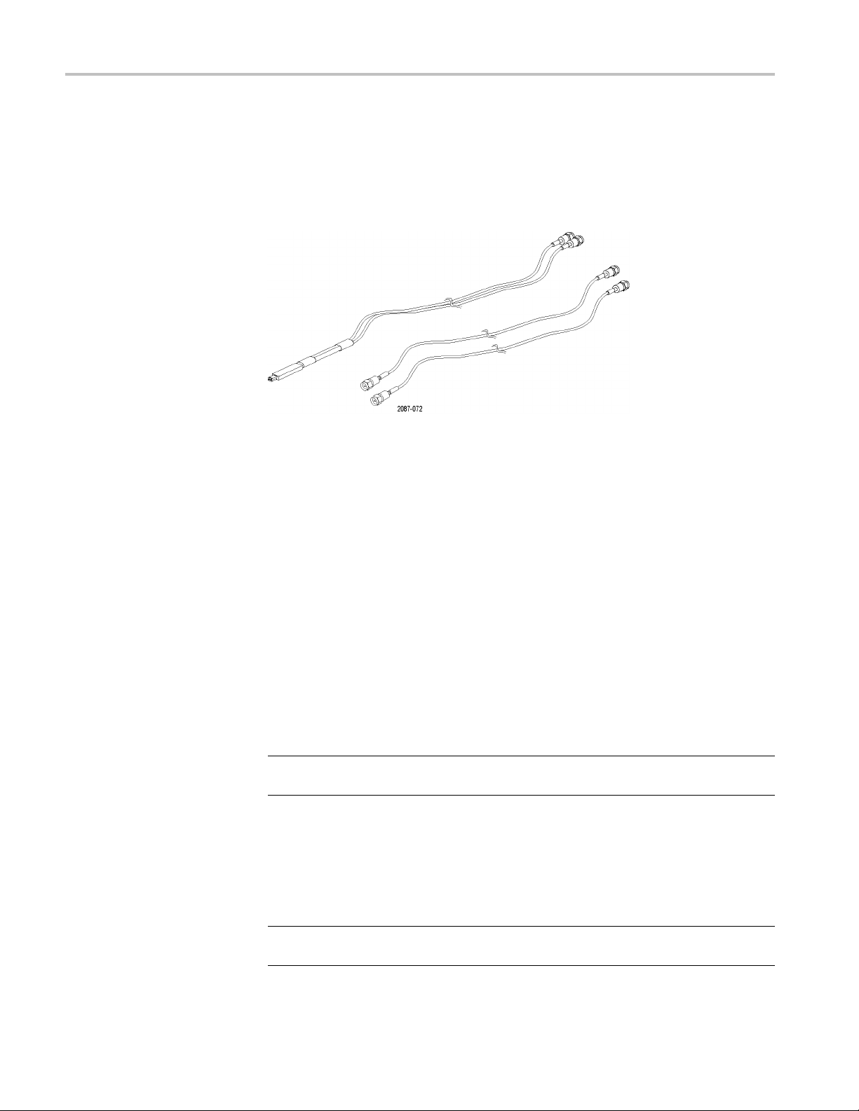
Figure 7: Arranging the midbus probe cables................ ................................ .................. 11
Figure 8: Connecting a slot interposer probe..................................... .............................. 12
Figure 9: Connecting a probe to the TLA7S16 Logic Protocol Analyzer................... ................ 15
Figure 10: Clock cable and clock jumper cable........ .................................. ...................... 16
Figure 11: Default Setup window ....................... .................................. ...................... 19
Figure 12: Assigning channels to lanes ....... .................................. ................................ 23
Figure 13: Default detector and listener channels on the probe connector................ .................. 25
Figure 14: L0s Detector settings . . . . . . . ..................... . . . . . . . . . . . . . . . . . ..................... . . . . . . . . . . . . . . . 25
Figure 15: Default Trigger window ............................................................................. 28
Figure 16: Specifying a TLP event .............................................................................. 30
Figure 17: Defining a TLP ....................................................................................... 30
Figure 18: Specifying a DLLP event............................................................................ 31
Figure 19: Defining a DLLP ..................................................................................... 31
Figure 20: Specifying a Link event................................ ................................ .............. 31
Figure 21: Defining a Link event .......... ................................ ................................ ...... 32
Figure 22: Specifying a symbol sequence ...................................................................... 33
Figure 23: Defining a symbol sequence................................. ................................ ........ 33
Figure 24: Event counter . ................................ ................................ ........................ 34
Figure 25: Specifying a global counter ............................... ................................ .......... 34
Figure 26: Specifying a timer .......... ................................ ................................ .......... 34
Figure 27: Transaction window.................................................................................. 38
ction........................... ................................ ............................ 57
Tektronix Logic Protocol Analyzer Solutions for PCI Express 2.0 Instruction Manual iii
Page 8

Table of Contents
Figure 28: Side
Figure 29: BEV with the Viewfinder and Location Bar....................................................... 42
Figure 30: BEV Configuration panel with Flow Control selected ........................... ................ 43
Figure 31: Opening the Summary Profile window .............................. .............................. 45
Figure 32: Summary Profile window................................ .................................. .......... 45
Figure 33: Summary Profile window (Summary Statistics Tab Notebook)................................. 46
Figure 34: D
Figure 35: Data displayed in the Listing window.............................................................. 49
-by-side Transaction window and Listing window .......................................... 40
efine Packet window for a Custom element in the Summary Profile window ............... 48
List of Tables
Table 1: Front panel indicators and connectors .................... ................................ ............. 2
Table 2: TLA7Sxx logic protocol analyzer module standard accessories.................................... 5
Table 3: TLA7Sxx logic protocol analyzer module service options .......................................... 5
Table 4: TLA7Sxx logic protocol analyzer compatible probes................................................ 7
5: TLA Modules and midbus probes per link ....................... ................................ ..... 9
Tabl e
Table 6: TLA Modules and slot interposer probes per link ......................... ........................... 9
Table 7: TLA Modules and solder down probes per link ........................... ........................... 9
Table 8: Status indicators in the Setup window ................................................................ 20
Table 9: Trigger events ........................................................................................... 29
Table 10: Trigger event recognizer resources ...................... ................................ ............ 29
le 11: Trigger actions ......................................................................................... 35
Tab
Table 12: Special characters in the Listing window ........... ................................ ................ 49
Table 13: Logic protocol analyzer disassembly display options ............................................. 50
Table 14: Training sequence messages.......................................................................... 52
Table 15: Packet framing messages ............. ................................ ................................ 52
Table 16: DLLP messages............ ................................ ................................ ............ 52
Table 17: TLP header messages ................................................................................. 52
Table 18: CRC checking messages .......................... ................................ .................... 53
Table 19: General acquisition messages . . .................... . . . . . . . . . . . . ................... . . . . . . . . . . . . . ...... 53
Table 20: Failure symptoms and possible causes .............................................................. 56
Table 21: Internal inspection checklist.......................................................................... 57
iv Tektronix Logic Protocol Analyzer Solutions for PCI Express 2.0 Instruction Manual
Page 9

General Safety Summary
General Safet
To Avoid Fire or Personal
Injury
ySummary
Review the fo
this product or any products connected to it.
To avoid pot
Only qualified personnel should p erform service procedures.
While using this product, you may need to access other parts of a larger system.
Read the safety s ections of the other component manuals for warnings and
cautions r
Use proper power cord. Use only the power cord specified for this product and
certified for the country of use.
Use proper voltage setting. Before applying power, ensure that the line selector
is in the proper position for the source being used.
Connect and disconnect properly. Do not connect or disconnect probes or test
leads while they are connected to a voltage source.
Ground the product. This product is grounded through the grounding conductor
of the power cord. To avoid electric shock, the grounding conductor must be
connected to earth ground. Before making connections to the input or output
terminals of the product, ensure that the product is properly grounded.
llowing safety precautions to avoid injury and prevent damage to
ential hazards, use this product only as specified.
elated to operating the system.
Observe all terminal ratings. To avoid fi re or shock hazard, observe all ratings
and markings on the product. Consult the product manual for further ratings
information before making connections to the product.
The inputs are not rated for connection to mains or Category II, III, or IV circuits.
Connect the probe reference lead to earth ground only.
Do not apply a potential to any terminal, including the common terminal, that
exceeds the maximum rating of that terminal.
Power disconnect. The power cord disconnects the product from the power source.
Do not block the power cord; it must remain accessible to the user at all times.
Do not operate without covers. Do not operate this product with covers or panels
removed.
Do not operate with suspected failures. If you suspect that there is damage to this
product, have it inspected by qualified service personnel.
Avoid exposed circuitry. Do not touch exposed connections and components when
power is pre sent.
Tektronix Logic Protocol Analyzer Solutions for PCI Express 2.0 Instruction Manual v
Page 10
General Safety Summary
TermsinThisManual
Symbols and Terms on the
Product
Do not operate i
Do not operate in an explosive atmosphere.
Keep product surfaces clean and dry.
Provide prop
on installing the product so it has proper ventilation.
These terms may appear in this manual:
WARNING.
in injury or loss of life.
CAUTION
damage to this product or other property.
These t
erms may appear on the product:
DANGER indicates an injury hazard immediately accessible as you read
the ma
n wet/damp conditions.
er ventilation. Refer to the manual's installation instructions for details
Warning statements identify conditions or practices that could result
. Caution statements identify conditions or practices that could result in
rking.
WARNING indicates an injury hazard not immediately accessible as you
the marking.
read
CAUTION indicates a hazard to property including the product.
The following symbol(s) may appear on the product:
vi Tektronix Logic Protocol Analyzer Solutions for PCI Express 2.0 Instruction Manual
Page 11

Service Safety S ummary
Service Safet
y Summary
Only qualifie
Safety Summary and the General Safety Summary before performing any service
procedures.
Do Not Service Alone. Do not perform internal service or adjustments of this
product unless another person capable of rendering first aid and resuscitation is
present.
Disconnect Power. To avoid electric shock, switch off the instrument power, then
disconnect the power cord from the mains power.
UseCareWhenServicingWithPowerOn. Dangerousvoltagesorcurrentsmay
exist in
disconnect test leads before removing protective panels, soldering, or replacing
components.
To avoid electric shock, do not touch exposed connections.
d personnel should perform service procedures. Read this Service
this product. Disconnect power, remove battery (if applicable), and
Tektronix Logic Protocol Analyzer Solutions for PCI Express 2.0 Instruction Manual vii
Page 12

Compliance Information
Compliance In
EMC C om pliance
EMC Compliance
Australia / New Zealand
Declaration of
Conformity – EMC
formation
This section
environmental standards with which the instrument complies.
Meets the intent of Directive 2004/108/EC for Electromagnetic Compatibility
when it is used with the product(s) stated in the specifications table. Refer to the
EMC specification published for the stated products. May not meet the intent of
the directive if used with other products.
European contact.
Tektronix UK, Ltd.
Western Peninsula
Western Road
Bracknell, RG12 1RF
United Kingdom
Complies with the EMC provision of the Radiocommunications Act per the
following standard, in accordance with ACMA:
CISPR 11:2003. Radiated and Conducted Emissions, Group 1, Class A, in
accordance with EN 61326-1:2006.
lists the EMC (electromagnetic compliance), safety, and
Safety Compliance
Equipment Type
Safety Class
Pollution Degree
Description
Test and measuring equipment.
Class 1 – grounded product.
A measure of the contaminants that could occur in the environment around
and within a product. Typically the internal environment inside a product is
considered to be the same as the external. Products should be used only in the
environment for which they are rated.
Pollution Degree 1. No pollution or only dry, nonconductive pollution occurs.
Products in this category are generally encapsulated, hermetically sealed, or
located in clean rooms.
Pollution Degree 2. Normally only dry, nonconductive pollution occurs.
Occasionally a temporary conductivity that is caused by condensation must
be expected. This location is a typical office/home environment. Temporary
condensation occurs only when the product is out of service.
viii Tektronix Logic Protocol Analyzer Solutions for PCI Express 2.0 Instruction Manual
Page 13

Compliance Information
Pollution Degree
Installation (Overvoltage)
Category Descriptions
Pollution Degr
that becomes conductive due to condensation. These are sheltered locations
where neither temperature nor humidity is controlled. The area is protected
from direct sunshine, rain, or direct wind.
Pollution Degree 4. Pollution that generates persistent conductivity through
conductive dust, rain, or snow. Typical outdoor locations.
Pollution Degree 2 (as defined in IEC 61010-1). Note: Rated for indoor use only.
Terminals on this product may have different installation (overvoltage) category
designations. The installation categories are:
Measurement Category IV. For measurements performed at the source of
low-voltage installation.
Measurement Category III. For measurements performed in the building
installation.
Measurement Category II. For measurements performed on circuits directly
connected to the low-voltage installation.
Measurement Category I. For measurements performed on circuits not
directly connected to MAINS.
ee 3. Conductive pollution, or dry, nonconductive pollution
Overvoltage Category
Overvoltage Category II (as defined in IEC 61010-1)
Tektronix Logic Protocol Analyzer Solutions for PCI Express 2.0 Instruction Manual ix
Page 14

Compliance Information
Environmenta
l Considerations
Product End-of-Life
Handling
Restriction of Hazardous
Substances
This section provides information about the environmental impact of the product.
Observe the following guidelines when recycling an instrument or component:
Equipment recycling. Production of this equipment required the extraction and
use of natural resources. The equipment may contain substances that could be
harmful to
end of life. To avoid release of such substances into the environment and to
reduce the use of natural resources, we encourage you to recycle this product in
an appropriate system that will ensure that most of the materials are reused or
recycled appropriately.
This product is classified as Monitoring and Control equipment, and is outside the
scope of the 2002/95/EC RoHS Directive.
the environment or human health if improperly handled at the product’s
This sym
Union requirements according to Directives 2002/96/EC and 2006/66/EC
on waste electrical and electronic equipment (WEEE) and batteries. For
informa
Tektronix Web site (www.tektronix.com).
bol indicates that this product complies with the applicable European
tion about recycling options, check the Support/Service section of the
x Tektronix Logic Protocol Analyzer Solutions for PCI Express 2.0 Instruction Manual
Page 15

Preface
Preface
Related Documentation
This manual d
escribes how to install and use a TLA7S16 or TLA7SA08 Logic
Protocol Analyzer Module and software with your PCI E xpress 2 system.
The following table lists related documentation, available f rom the Tektronix
Web site (www.tektonix.com/manuals).
The TLA7S08 & TLA7S16 Series Product Specifications and Performance
Ver i fication Technical Reference Manual (Tektronix part number 077-0114-xx)
lists the product specifications and h igh-level functional check procedures for
your TLA7S16 or TLA7S08 Logic Protocol Analyzer Module.
The P6700 Series Serial Analyzer Probes Instruction M anual (Tektronix
part number, 077-0115-xx) provides instructions for using the P6700 Series
Serial Analyzer Probes with your TLA7S16 or TLA7S08 Logic Protocol
Analyz
er Module.
Related documentation
Item Purpose
TLA Quick Start User Manuals
Online Help
Installation Reference Sheets High-level installation information
Installation Manuals
XYZs of Logic Analyzers
Declassification and Securities instructions Data security concerns specific to sanitizing
Application notes
Product Specifications & Performance
Verification Procedures
TPI.NET Documentation
Field upgrade kits
Optional Service Manuals Self-service documentation for modules and
High-level operational overview
In-depth operation and UI help
Detailed first-time installation information
Logic analyzer basics
or removing memory devices from Tektronix
products
Collection of logic analyzer application
specific notes
TLA Product specifications and performance
verification procedures
Detailed information for controlling the logic
analyzer using .NET
Upgrade information for your logic analyzer
mainframes
Tektronix Logic Protocol Analyzer Solutions for PCI Express 2.0 Instruction Manual xi
Page 16

Preface
xii Tektronix Logic Protocol Analyzer Solutions for PCI Express 2.0 Instruction Manual
Page 17

Getting Started
Product Descr
TLA7S16 x8 Logic Protocol
Analyzer Module
TLA7S08 x4 Logic Protocol
Analyzer
iption
Module
The TLA7S08 & TLA7S16 Logic Protocol Analyzer Modules acquire and
analyze PCIe2 and PCIe1 data at acquisition rates of 5.0 GT/s and 2.5 GT/s.
They provid
The m odules acquire up to 32 million 8b/10b symbols or bytes-per-line. The main
difference between the modules are the number of inputs.
The TLA7S
supports x1, x2, x4, and x8 links.
The TLA7S08 Logic Protocol Analyzer Module has 8 differential inputs and
support
e packet-level triggering, sequence triggering, and error triggering.
16 Logic Protocol Analyzer Module has 16 differential inputs and
s x1, x2, and x4 links.
Figure 1: P67S16 x8 midbus probe
Tektronix Logic Protocol Analyzer Solutions for PCI Express 2.0 Instruction Manual 1
Page 18

Getting Started
Logic Protoco
l Analyzer Module Controls and Connectors
This section briefly describes the logic protocol analyzer controls and connectors.
Front Panel
The front panel provides indicators for checking the status of the logic protocol
analyzer. It includes probe connectors, two probe power connectors, and four
connectors for a reference clock. The TLA7S16 has four probe connectors. (See
Figure 2 on page 3.) The TLA7S08 has two probe connectors. A description of
the indica
tors and connectors is provided in the following table. (See Table 1.)
The functions of the indicators and connectors are the same for both modules
except where noted.
Table 1: Front panel indicators and connectors
Item
number Indicator or connector Description
1 READY indicator
2
3 ARM'D indicator The ARM’D indicator lights when the logic protocol analyzer module is armed during
4
5
6
7
8 Probe Power connectors The probe power connectors provide power to the probes.
ACCESSED indicator The ACCESSED indicator lights anytime the controller accesses the logic protocol
TRIG'D indicator The TRIG’D indicator lights when the logic protocol analyzer module triggers and stays on
Probe connectors
Reference Clock Output
connectors
Reference Clock Input
connectors
The READY indicator lights continuously after the logic protocol analyzer module
successfully completes the power-on process. If the indicator fails to light within five
seconds of power-on, an internal module failure may be present.
analyzer module.
an acquisition.
until the module finishes acquiring data.
Four connectors for the TLA7S16 module (two for the TLA7S08 module) provide the
probe connections for the module. Each connector is labeled with a letter A, B , C, or D
for the TLA7S16 module (A or B for the TLA7S08 module). The letters correspond to
the graphic display in the Setup window.
The Reference Clock Output SMA connectors (labeled + and – ) provide a means of
passing the differential clock signal from the Reference Clock Input connectors to another
external module.
Two SMA connectors (labeled + and – ) provide differential clock input connections from
the SUT or from another module.
2 Tektronix Logic Protocol Analyzer Solutions for PCI Express 2.0 Instruction Manual
Page 19

Getting Started
Figure 2: TLA7S16 logic protocol analyzer front panel
Tektronix Logic Protocol Analyzer Solutions for PCI Express 2.0 Instruction Manual 3
Page 20

Getting Started
Rear Panel
The rear panel p
The rear panel includes two logical address switches. (See Figure 3 on page 4.)
Tektronix recommends that you leave the switches at the default switch setting
of FF (Dynamic Auto Configuration). When the switches are set to FF, the
instrument automatically sets the address to an unused value.
NOTE. Do not set any module to logical address 00. Logical address 00 is
reserved ex
rovides connectors to connect the module to the mainframe.
clusively for the controller.
Figure 3: TLA7S16 rear panel
4 Tektronix Logic Protocol Analyzer Solutions for PCI Express 2.0 Instruction Manual
Page 21

Getting Started
Logic Protoco
l Analyzer Compatibility
Install the TLA7S08 & TLA7S16 Logic Protocol Analyzer modules in either a
TLA7012 portable mainframe logic analyzer, or a TLA7016 benchtop mainframe
logic analyz
installed, and the latest version of the TMS160PCIe2 Tektronix PCI Express
Support Software.
Options and Accessories
The following table lists the accessories for the TLA7S16 Logic Protocol
Analyzer Modules and TLA7S08 Logic Protocol Analyzer Modules.
Table 2: TLA7Sxx logic protocol analyzer module standard accessories
Accessory
Reference clock cable, SMA-to-3 pin header
Cable assembly, reference clock jumper
The following table lists the service options for the modules and probes.
Table 3
er. The logic analyzer must have TLA Software V5.7 or higher
Tektronix
part number
672-6285-xx
174-5392-xx
: TLA7Sxx logic protocol analyzer module service options
Service Offerings
Repair warranty extended to cover three years (including warranty)
Repair warranty extended to cover five years (including warranty)
Single calibration event or coverage CA1
Calibration services extended to cover three years C3
Calibration services extended to cover five years C5
Installing the Tektronix Logic Protocol Analyzer Module
This manual is written assuming that your logic analyzer mainframe is already
installed properly. However, a high-level module installation overview is
provided. If you need additional help installing your mainframe, refer to the
TLA7000 Series Logic Analyzers Installation Manual.
CAUTION. To avoid damaging the mainframe, do not install or remove any
modules while the mainframe is powered on. Always power off the instrument
before installing or removing modules.
Cover any empty module slots with a blank cover (Tektronix part number,
333-4206-xx).
Option
number
R3
R5
Tektronix Logic Protocol Analyzer Solutions for PCI Express 2.0 Instruction Manual 5
Page 22

Getting Started
Install the mod
the retaining screws to 2.5 in-lbs after seating the modules in place.
ules in the mainframe. (See Figure 4.) Use a screwdriver to tighten
Figure 4: Installing a module
6 Tektronix Logic Protocol Analyzer Solutions for PCI Express 2.0 Instruction Manual
Page 23

Getting Started
List of Compat
ible Probes
The following probes are compatible with the logic protocol analyzer module:
Table 4: TLA7Sxx logic protocol analyzer compatible probes
Probe Description
P6708 x4 Midbus probe
P6716 x8 Midbus probe
P6701S
P6704S
P6708S
P6716S
P6701SD Solder-down probe, one differential pair
For deta
Instruction Manual.
iled information on these probes, refer to the P67xx Series Probe
Connecting the Instrument to the SUT
The probes connect your logic protocol analyzer module to the SUT. The
following illustration shows possible connections to your SUT. Choose the
probing scheme that works for your application. (See Figure 5 on page 8.)
x1 slot interposer probe
x4 slot interposer probe
x8 slot interposer probe
x16 slot interposer probe
Tektronix Logic Protocol Analyzer Solutions for PCI Express 2.0 Instruction Manual 7
Page 24

Getting Started
Figure 5: Installation overview
The following tables list the number of probes needed per module to connect to a
k. Refer to the previous illustration for an overview of the connections to the
lin
logic analyzer and SUT. (See Figure 5 on page 8.)
ditional probe connection information is provided later in this document; refer
Ad
to those sections for additional information.
8 Tektronix Logic Protocol Analyzer Solutions for PCI Express 2.0 Instruction Manual
Page 25

Getting Started
Table 5: TLA Mod
Link TLA M od ules Probes
x16
x8
ules and midbus probes per link
1 TLA7S16 1 P67S16
1 TLA7S16 or 1
TLA7S08
1 P67S16 or P6
Table 6: TLA Modules and slot interposer probes per link
Link TLA M od ules Probes
x16
x8
x4, or x2
x1
Table 7:
Link TLA Modu
x16
x8
x4
x1
2 TLA7S16 1 P67S16S
1 TLA7S16 or 2 TLA7S08 1 P67S08S
1 TLA7S16 or 1 TLA7S08 1 P67S04S
1 TLA7S16 or 1 TLA7S08 1 P67S01S
TLA Modules and solder down probes per link
16
2TLA7S
1 TLA7S
1 TLA7
1 TLA7
16 or 1 TLA7S08
S16 or 1 TLA7S08
S16 or 1 TLA7SA08
les
Probes
16 P67S
8 P67S0
4 P67S
1 P67S
01SD
01SD
7S08
01SD
1SD
Handling the Probe Heads
Handle the probe heads with care. Keep the following points in mind:
NOTE. Be careful when handling the probe heads while the midbus probe is
connected to a powered module. The probe head may become warm to the touch;
the probe is operating normally.
CAUTION. Static discharge can damage the probe heads. Always wear a
grounded antistatic wrist strap whenever handling the probe heads. Also verify
that anything to which the probe heads are connected do not carry a static charge.
Handle the probe heads by the outer casing. Do not touch the contacts in the
center with fingers, tools, wipes, or any other devices.
Do not expose the connector to liquids or dry chemicals.
When connecting the probes, be careful not to touch the probe head contacts
to any other surfaces or components on your circuit board.
Tektronix Logic Protocol Analyzer Solutions for PCI Express 2.0 Instruction Manual 9
Page 26

Getting Started
Connecting th
eMidbusProbetotheSUT
Follow these steps to connect a midbus probe to the retention mechanism on
your circuit board:
1. Locate the correct retention mechanism. If you intend to use multiple probes,
your PCB has multiple retention mechanisms. Be careful to select the correct
one.
2. Align the probe head with the retention mechanism. Both are keyed so that
the probe c
3. Press the probe head into the retention mechanism.
an only be inserted one way.
Figure 6: Connecting a probe to the retention mechanism
10 Tektronix Logic Protocol Analyzer Solutions for PCI Express 2.0 Instruction Manual
Page 27

Getting Started
4. Start both moun
that the probe approaches and mates squarely to the PCB. Use the adjustment
tool included with your probe. Proper installation torque is 1 in-lb.
5. Hang the probe cables so that the probe head is perpendicular to the circuit
board, and tension on the retention mechanism is minimized. Route the
cables as straight as possible, maximizing the bend radius, and making sure
that a 90 degree bend does not occur within three inches of the circuit board
surface. (SeeFigure7.)
ting screws in the posts, and tighten them evenly to ensure
Figure 7: Arranging the midbus probe cables
Connecting a Slot Interposer Probe to the SUT
Connect a slot interposer probe to a PCI Express slot on your SUT by following
ese steps:
th
CAUTION. Connecting the slot probe head to a powered SUT can damage the slot
probe. Do not hot-plug the slot interposer probe head into a powered SUT. Always
power off the SUT before installing the slot probe head into the SUT.
Tektronix Logic Protocol Analyzer Solutions for PCI Express 2.0 Instruction Manual 11
Page 28

Getting Started
1. Disconnect the
your SUT is connected to one.
2. Locate the cor
3. Remove the PCI Express card that is in the PCI Express slot of the SUT.
4. Align the probe head with the slot.
5. Press the probe head into the slot.
NOTE. Remove the slot probe bracket if it interferes with the add-in PCI Express
card.
6. Position the mounting bracket and attach the screws.
7. Press yo
ur PCI Express card device into the probe.
power supply to your SUT. Disconnect the PC power supply if
rect PCI Express slot.
gure 8: Connecting a slot interposer probe
Fi
12 Tektronix Logic Protocol Analyzer Solutions for PCI Express 2.0 Instruction Manual
Page 29

Getting Started
Connecting a Probe to a
x16 Link
To ca pture sign
slot interposer probe. Connect the probe by following these steps:
CAUTION. Connecting the slot probe head to a powered SUT can damage the slot
probe. Do not hot-plug the slot interposer probe head into a powered SUT. Always
power off the SUT before installing the slot probe head into the SUT.
1. Disconnect the power supply to your SUT. If your SUT is connected to a PC
power supply, disconnect the power supply.
2. Locate the correct PCI Express slot.
3. Remove the PCI Express card that is in the PCI Express slot of the SUT.
4. Align the probe head with the slot.
5. Press th
NOTE. Remove the slot probe bracket if it interferes with the add-in PCI Express
card.
als from a x16 link you need to connect two modules to a single
e probe head into the slot.
Tektronix Logic Protocol Analyzer Solutions for PCI Express 2.0 Instruction Manual 13
Page 30

Getting Started
6. Position the mo
7. Press your PCI Express card device into the probe.
8. Connect the probe to the two modules and connect the probe power connector
to both modules.
NOTE. The x1
connector to the same module as the respective data connectors. Pay attention
to labels on the probe power connectors when connecting them to the module.
The modules must be powered on whenever the SUT is powered on for the PCI
Express signals to reach the PCI Express card connected to the probe.
unting bracket and attach the screws.
6 slot probe has two power connectors. Connect the power
Connecting the Solder Down Probe
The prob
is soldered to the circuit. Refer to the P6700 Series Serial Analyzer Probes
Instruction Manual for additional information on using the P67SA01 solder-down
probe and accessories.
e connects to the module and to the probe tip, and the probe tip
Connecting the Probes to the Logic Protocol Analyzer Module
Follow these steps to connect a probe to the logic protocol analyzer module:
1. Connect the module ends of the probe from the downstream data link to the
logic protocol analyzer module that will acquire the downstream data. (See
Figure 9 on page 15.)
a. Plug the probe connector labeled 0, 2, 4, and 6 (channels) into the top
connector on the module (A).
b. Plug the probe connector labeled 1, 3, 5, and 7 (channels) into the second
connector (B).
c. Plug the probe connector labeled 8, 10, 12, and 14 (channels) into the
third connector (C).
d. Plug the remaining probe connector into the fourth connector (D) on the
module.
2. Connect the probe power connectors to the power connectors on the front
panel of the module.
3. Tighten the connector screws using the adjustment tool included with your
probe.
14 Tektronix Logic Protocol Analyzer Solutions for PCI Express 2.0 Instruction Manual
Page 31

Getting Started
Figure 9: Connecting a probe to the TLA7S16 Logic Protocol Analyzer
Tektronix Logic Protocol Analyzer Solutions for PCI Express 2.0 Instruction Manual 15
Page 32
Getting Started
Clock Cable
Two clock connection cables are included with your logic protocol analyzer
module. One is for connecting the reference clock input of the module to the
SUT or slot in
module to another.
Figure 10: Clock cable and clock jumper cable
terposer probe, and the other is a jumper cable for connecting one
Connecting a Cloc k Cable
Connecting a Clock
Jumper Cable
Connect a clock cable by following these steps:
1. Connect one end of the cable to the Ref Clock input connectors (+ and –) on
the logic protocol analyzer module; screw the SMA connectors down until
they are snug.
2. Connect the other end of the correct cable to the SUT three-pin connector or
the slot interposer probe three-pin connector.
1. Connect one end of the cable to the Ref Clock input connectors (+ and –) on
the logic protocol analyzer module; screw the SMA connectors down until
they are snug.
2. Connect the other end of the cable to the Ref Clock output connectors
(+and–)onanothermodule.
NOTE. Clock Reference Source must be set to SUT if either clock cable is used.
(See page 21, Selecting a Clock Signal Source.)
Applying and Removing Power
After you have connected all probes to the SUT, you are ready to apply power to
the SUT and the logic protocol analyzer.
NOTE. When using slot interposer probes power on the logic protocol analyzer
before applying power to the SUT.
16 Tektronix Logic Protocol Analyzer Solutions for PCI Express 2.0 Instruction Manual
Page 33

Install the TMS160PCIe2 Support Software
After completing the hardware setups, install the support software.
NOTE. Before you use the logic protocol analyzer, verify that your mainframe
has the most
Software. The TLA Application software must be installed on all mainframes and
PCs that will use the logic protocol analyzer modules, including any PCs that
will remotely control the logic protocol analyzer. (See page 61, TLA Application
Software.)
To use the TMS160PCIe2 Support Software, install the following CDs:
TMS160PCIe2 Support Software CD, Tektronix part number 063-4266-xx.
TMS160xxxx TLA Add-On Data Windows Software CD, Tektronix part
number 063-4326-xx.
Follow these steps to install the software:
current TLA Application software and the TMS160PCIe2 Support
1. Inser
2. Start Windows Explorer, navigate to the media drive and execute the file
3. Click Yes to start the installation and follow the on-screen instructions. If you
4. Remove the TMS160PCIe2 Support Software CD from the media drive and
5. Using Windows Explorer, navigate to the media drive and execute the file
6. Follow the on-screen instructions to install the software.
7. Remove the CD when the installation is complete.
8. After you start the TLA and connect to the mainframe, a message might
t the TMS160PCIe2 Support Software CD in the media drive.
TMS16
are a
ins
TM
appear instructing you to update the module firmware. If so, update the
module firmware before continuing. (See page 61, Updating the Logic
Protocol Analyzer Module Firmware.)
0PCIE2_Setup.exe.
sked for permission to overwrite any read-only files, select Ye s t o A ll.
ert the TMS160xxxx TLA Add-On Data Windows Software CD.
S160View_Setup.exe.
Tektronix Logic Protocol Analyzer Solutions for PCI Express 2.0 Instruction Manual 17
Page 34

Using the Logic Protocol Analyzer
Using the Logic Protocol Analyzer
Refer to the information earlier in this document for installing common hardware,
connecting the instrument to the SUT, and connecting probes to the SUT to and
the logic pro
The basic steps for using logic protocol analyzer are summarized below:
1. Use the Setup window to view signal activity, automatically configure the
instrument, and to calibrate the probes.
2. If necessary, specify the triggering in the Trigger window or use the default
trigger setups.
3. Acquire and validate initial data in the Transaction and Listing display
windows.
4. Use the Summary Profile window together with the Transaction and Listing
windows, and related debugging tools to analyze high-level transaction
inform
acquisition.
tocol analyzer.
ation linked to lowest-level physical layer symbols across the entire
Logic Protocol Analyzer Setup Window
The Setup window provides easy access to a variety of configuration options to
do the following:
Acquire bidirectional data.
cify the link width and transfer rate.
Spe
Use a clock embedded in the data stream or use an external clock connected
the front panel.
to
Establish storage conditions such as hardware filtering, link scrambling and
skewing, specifying the storage length, and specifying the trigger position.
de
Establish which modules are associated to links.
Open the Setup Window
The Setup window is the default window when you first power on the logic
protocol analyzer. If your system includes more than one logic protocol
analyzer module, the system displays the Setup window for the module in the
lower-numberd slot.
18 Tektronix Logic Protocol Analyzer Solutions for PCI Express 2.0 Instruction Manual
Page 35

Using the Logic Protocol Analyzer
If the Setup win
methods:
Click the Setu
By default the first logic protocol analyzer is identified as SA 1.
Click the Setup button in the System Navigation toolbar.
If your system has more than one module, select the appropriate module from
the Setup button.
Click the Setup button on the Logic Protocol Analyzer icon in the System
window.
Click Setup: SA 1 in the Window menu.
The default Setup window is shown below. (See Figure 11.) The color of the
status indicators near the center of the window will vary depending on the signal
y at the probe tip.
activit
dow does not display, open the window using one of the following
pIconintheTLAExplorer.
Figure 11: Default Setup window
Tektronix Logic Protocol Analyzer Solutions for PCI Express 2.0 Instruction Manual 19
Page 36

Using the Logic Protocol Analyzer
Monitoring Si
gnal Activity
After you have connected the probes and installed the software and firmware,
monitor the signal activity on each of the lanestomakesurethatyoursystem
is operating
representation of the logic protocol analyzer module shows a status indicator for
each lane. Use the status indicators to determine if the SUT produces the signals
that the module can recognize. The logic protocol analyzer constantly monitors
the status of each lane, even when data is not being acquired.
A description of each status indicator is listed below.
Table 8: Status indicators in the Setup window
Indicator Description
correctly and that the probes are connected properly. A graphic
No signal (gray). A signal has not been assigned to a lane.
(See page 22, Assigning Lanes.)
Signal missing. The signal is assigned to a lane, but it is not
recognized. This symbol appears when a lane is inactive.
Signal (yellow). A signal is detected, but not locked. The data
is not recognized.
Data signal (green). A signal is detected and recognized as
data.
Clock signal. A clock signal is detected via the clock cable
connected to the SUT or slot interposer probe. The colors
and patterns of the clock signal indicator function similar to
those of the other status indicators.Thisindicatorisgrayif
the SUT Reference Clock selection is set to Not Used. (See
page 21, Selecting a Clock Signal Source.)
Defining the Link
To de fine a link, specify the following information about your SUT; define one
link per module:
Link name. The default link name is Link1. Double-click on the Link tab to
enter a meaningful name.
Autoset. After the link has completed a training sequence, the Autoset button in
the Status area becomes active. Click Autoset to automatically complete the
setup for the entire link.
Acquire. Select one of the Acquire buttons to identify the upstream and
downstream lanes for capturing data. The selection that you make impacts the
appearance of the lane assignments on the right side of the Setup window. For
example, if you select downstream data, the upstream lane assignments become
unavailable.
20 Tektronix Logic Protocol Analyzer Solutions for PCI Express 2.0 Instruction Manual
Page 37

Using the Logic Protocol Analyzer
Selectin
g a Clock Signal
Source
Switch Sides. U
between the downstream and upstream sides.
Maximum Link Width. Specify the maximum number of lanes in your link.
Transfer Rate. Tektronix recommends setting Transfer Rate to Track Training
(default) w
logic protocol analyzer module recognizes data as the link trains up in speed
from 2.5 GT/s to 5.0 GT/s. If you intend to more closely observe the data rate
transition, set Transfer Rate to 2.5 GT/s or 5.0 GT/s. The logic protocol analyzer
will only recognize data at that rate, but it will recognize data for a longer period
of time during the transition.
The logic protocol analyzer can recognize a clock signal from a cable connection
to the SUT (or slot interposer probe), or by recovering the clock signal embedded
in the data.
Recognize the clock signal embedded in the data stream. To use an embedded
clock signal, set the SUT Reference Clock selection to Not Used.Astable
reference signal is generated by the logic protocol analyzer and synchronizes with
the embedded clock signal. A clock cable connection is not required, since the
logic protocol analyzer recognizes the embedded signal from the probe.
se the Switch Sides button to quickly switch the lane assignments
hen analyzing a bus operating at PCI Express Gen2 specifications. The
Storage Settings
Recognize the clock signal by directly connecting to the SUT with a clock
cable. Tektronix recommends connecting a clock cable to make sure that data
is accurately synchronized with the clock signal. Set the SUT Reference Clock
selection to Connected at Front Panel and then select an approximate frequency
for your application. Make sure the reference clock cable is connected correctly.
ee page 16, Connecting a Clock Cable.)
(S
NOTE. If SSC (spread-spectrum clocking) is enabled, and your PCI Express link
uses power management states, you must connect a clock cable to the SUT and
set the reference clock source to Connected at Front Panel to ensure that all
symbols are recognized by the logic protocol analyzer during the transition from a
power management state to the L0 state.
An external clock is also required to conduct frequency margin testing when the
SUT is operating at rates other than 2.5 GT/s or 5 GT/s.
Specify the amount of data to store (symbols per lane), and set the trigger position
relative to the amount of data stored. A trigger position setting of 0% indicates
that data will be stored after the trigger event occurs. A trigger position setting of
100% indicates that data storage will stop when the trigger event occurs.
Tektronix Logic Protocol Analyzer Solutions for PCI Express 2.0 Instruction Manual 21
Page 38

Using the Logic Protocol Analyzer
Descramble and Desk ew
Defining a Data Filter
Assigning Lanes
The following g
Link Data Storage area:
NOTE. Only 8b data is available for triggering.
Data can not be descrambled unless Store as: 8b Data is selected.
Select Descramble to store data in a descrambled format.
Select Store as 10b Data to store data in 10b format (a post-processing
operation).
Select Store as 8b Data to store the more conventional 8b data.
Select Deskew Lanes to view time-aligned lane data in the listing window.
The Setup window provides a means of filtering data to focus o n the data you are
ted in. Select a predefined data filter from the list, or click Define Filter and
interes
select what you want to filter from the data stream. Click OK when you are done.
On the right side of the Setup window, the graphic representation of the logic
col analyzer module shows the lane mapping (lines drawn between numbered
proto
lanes and channels depending on the number of lanes in use). If you click Autoset,
the logic protocol analyzer maps the lanes to thr channels to based on the current
trained link configuration; it also updates the Acquire and Maximum Link Width
selections. If you want to change the lane mapping, click and drag the lines so that
the signals are connected to the lanes as your design dictates.
uidelines provide information when you should select items in the
A line connects each signal to a lane so that data will be recorded and displayed
properly in the data windows. Unless all connected indicators are green, the logic
otocol analyzer will not be able to identify packet structures correctly.
pr
NOTE. If you have a bidirectional link, one side of the link (upstream or
downstream) must be connected to channels of the top two connectors on a
16-channel module, or the top connector on an 8-channel module. The other side
of the link must be connected to the other connector(s).
22 Tektronix Logic Protocol Analyzer Solutions for PCI Express 2.0 Instruction Manual
Page 39

Using the Logic Protocol Analyzer
e 12: Assigning channels to lanes
Figur
orm the following steps to map the input channels to lanes:
Perf
1. Determine the correlation between each lane and input channel.
2. Select the left edge of the input channel indicator.
The left edge becomes highlighted to show that it has been selected.
3. Drag the left edge of the channel indicator to the appropriate lane indicator
on the right.
When you release the mouse button, a solid line connects the two indicators
together.
4. Repeat the above steps for each channel indicator and lane connector.
Tektronix Logic Protocol Analyzer Solutions for PCI Express 2.0 Instruction Manual 23
Page 40

Using the Logic Protocol Analyzer
SpecificC
Degrada
tion, and Link Training
5. To change the po
NOTE. The plus/minus sign is a polarity setting, not an indicator of polarity.
6. If data is bei
to a lane will turn green (data signal recognized). If data is not being
transmitted but a signal is present, the indicators will turn yellow. Gray
indicators with red stripes indicate that the channel has been properly assigned
to the lane, but a signal is missing.
Indicators must be green for d ata to be recorded and analyzed in the Waveform
or Listing window.
larity of a channel, click the center of the indicator.
ng transmitted on the bus, the indicator of each channel assigned
onsiderations for Testing Link Power Management States, Link
If you intend to observe the timing of link transitions (link width, power savings
state transitions, lane reversal) there are certain considerations about the logic
ol analyzer module that must be noted.
protoc
Detector Channels and
Listener Channels
The logic protocol analyzer can accurately detect when a link transitions to
and from a link state where no data is transmitted on the link. The instrument
gnizes these link transitions by detecting the presence or absence of electrical
reco
signals only on lanes connected to the top and bottom channel on each connector
(two of the four channels on each connector). All other channels infer the presence
or absence of electrical signals by "listening to" these channels. By default, each
of the two listener channels on each connector are set to listen to one of the two
detector channels on that connector.
Any listener channel on connector A or B can be assigned to listen to any detector
channel on connector A or B. Any listener channel on connector C or D can
e assigned to listen to any detector channel on connector C or D (16-channel
b
module only).
n each probe connector the top and bottom channels are defined as detector
O
channels. The center two channels of each connector are defined as listener
channels. The default settings for each connector are shown in the following
illustration, in this case for the A probe connector. (See Figure 13.) To view or
edit the detector settings, right click and select Define Electrical Idle Detection
Method.
24 Tektronix Logic Protocol Analyzer Solutions for PCI Express 2.0 Instruction Manual
Page 41

Using the Logic Protocol Analyzer
Figure 13: Default detector and listener channels on the probe connector
Figure 14: L0s Detector settings
You should not need to change any settings for most configurations. Tektronix
recommends that you use the standard (default) settings. If necessary, manually
change the settings. Some link configurations will require that you change the
ector channel that a listener channel listens to, while very few configurations
det
will require you to rewire the module-end probe c onnector.
general, any time that the link transitions to a x 2 or x1 width, and Lanes 0 or 1
In
are no longer connected to detector channels, the link will appear to be in an idle
state when it is not. Be aware when this situation occurs and follow the suggested
link formats that are provided in the P67xx Series Probes Instruction Manual.
Contact your local Tektronix representative for assistance.
Tektronix Logic Protocol Analyzer Solutions for PCI Express 2.0 Instruction Manual 25
Page 42

Using the Logic Protocol Analyzer
Changing the Maximum
Electrical I
dle Timeout
Bypassing the Transition
Detectors
To temporarily
transition detection rate, turn off the L0s detection. (See Bypassing the Detectors.)
When the Transfer Rate is set to Track Training and an electrical idle occurs
longer than t
5GT/sto2.5GT/s. AnelectricalidlecanhappenwhentheSUThasshutdown
and starts up again in 2.5 GT/s mode.
Some applications return to an electrical idle after a preset timeout period.
The circuits should have returned from an L1 state within the timeout period.
However, some tests might require a longer timeout setting. Use the Maximum
Idle Time Detector to specify the maximum timeout for your application. To view
or set the timeout setting, right-click the mouse in the Channel-Lane Assignment
area of t
Adjust the timeout setting in the Define Electrical Idle Transition Detection
window. (SeeFigure14onpage25.)
Select
instrument in a troubleshooting/debugging mode. The electrical idle detectors are
bypassed, and signal activity on all lanes is recognized. However, this mode
inhibits the speed at which the link recovers from an L0s state (up to 6 μs).
When you have finished troubleshooting or debugging and are ready to begin
acquiring data, disable the selection by selecting Standard - Automatic detector
ass
he Setup window and select Define Electrical Idle Detection Method.
Off - Disables fast electrical idle transition detectors to place the
ignment (Recommended).
bypass the detectors to observedataonalllanesataslower
he specified timeout, the module switches the acquistion rate from
Using Timestamp
Averaging
Here is an example of a situation when you should use this setting:
A x4 link on a mid-bus footprint has been mistakenly wired in a non-standard
format, so that Lane 0 is connected to Channel 1 instead of Channel 0
onnector A). It is not clear where Lane 0 is. Channel 1 listens to Channel 0
(c
(default), but when the link trains down to a x1 (on Channel 1), Channel 1 is
listening (and detecting) an electrical idle signal on Channel 0. It appears that
the link is in an electrical idle state when it is not. When you turn the detection
off, you can see that the footprint or the module-end probe connector must
be rewired.
When using bi-directional storage, both sides of the link are essentially ORed
together to determine when the storage should occur. If you enable Timestamp
Averaging, both sides o f the link must work together to calculate the average
timestamp. (Problems can occur if one side of the link enters or exits the electrical
idle state and the other link resets its alignment. For example, when a down-side
link enters or exits an electrical idle state, the up-side link becomes misaligned
because the FIFOs on the down-side link must be reset.)
26 Tektronix Logic Protocol Analyzer Solutions for PCI Express 2.0 Instruction Manual
Page 43

Using the Logic Protocol Analyzer
To avoid proble
electrical idle states, Tektronix recommends that you disable the Timestamp
Averaging feature (right-click the mouse in the Setup window to display the
context menu and clear the Timestamp Averaging selection).
Disabling Timestamp Averaging allows each side of the bus to track alignment
and revert to a series of bursts. The burst samples are separated by 1.8 ns followed
by time gaps in the range of 10 ns to 100 ns.
Trigger Wi
ndow
After defining parameters in the Setup window, define a trigger that tells the logic
protocol analyzer when to begin recording data. The logic protocol analyzer
provides
specify trigger conditions on any field within a packet.
Open the Trigger Window
NOTE. The instrument has a separate Trigger window for each installed module.
Make sure that you select the Trigger window that applies to your module.
ms when using bidirectional links with buses entering or exiting
powerful triggering capabilities including predefined trigger templates to
Open the Trigger window by doing one of the following:
Click the Trigger icon in the TLA Explorer.
By default the first logic protocol analyzer is identified as SA 1.
Select the Logic Protocol Analyzer from the Trigger button in the TLA toolbar.
ck the Trigger button on the Logic Protocol Analyzer icon in the System
Cli
window.
ick Trigger: SA 1 in the Window menu.
Cl
Click Define Trigger in the Setup window.
Tektronix Logic Protocol Analyzer Solutions for PCI Express 2.0 Instruction Manual 27
Page 44
Using the Logic Protocol Analyzer
Quick Tips
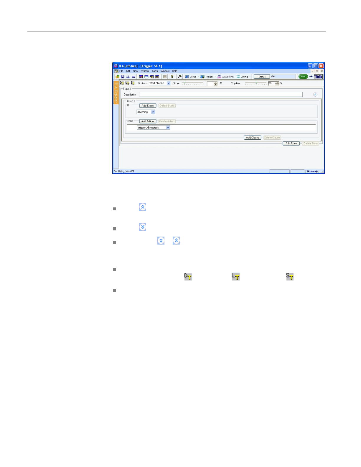
The default Tri
Figure 15: Default Trigger window
Click to collapse the current trigger state to provide more room on the
screen.
gger window is shown below. (See Figure 15.)
Adding States, Clauses,
Events, and Actions
Click to
Look fo
They are indicators that there may be more or less information to display
on screen.
Click one of the three icons at the top of the Trigger window to open the
default trigger window
The Store and Trigger Position controls are identical to those in the Setup
window.
A trigger definition is a logical expression consisting of events and actions within
clauses, within states. The default Trigger window starts with one state (State 1).
and one clause (Clause 1). A trigger definition can have up to eight trigger states
with eight trigger clauses per state. To work with states, clauses, events, and
actions, do the following:
1. Begin editing the clause by selecting Events (IF) and Actions (THEN).
2. To add additional events or actions to the clause, click Add Event or Add
Action.
3. Multiple events can be joined by a logical AND or an OR. Click AND to
changeittoanOR.ActionscanonlybejoinedbyanAND.
expand the current trigger state.
rthe
or to expand or collapse information in the current Clause.
, load a trigger , or save a trigger .
28 Tektronix Logic Protocol Analyzer Solutions for PCI Express 2.0 Instruction Manual
Page 45

Using the Logic Protocol Analyzer
Deleting States, Clauses,
Events, and Actions
Trigger Events
4. To add another c
lause or state, click Add Clause or Add State.
5. Add states, clauses, events, and actions by right-clicking and selecting from
the context me
nu.
Delete states, clauses, events, and actions by clicking the appropriate button in the
Trigger window, selecting from the Edit menu, or by right-clicking and selecting
from the con
text menu.
Trigger events are listed in the following table.
Table 9: Trigger events
Event D escription
Anything Recognizes any data.
TLP
DLLP
Seque
Link E
Timer
nter
Cou
nal In
Sig
nce
vent
Recognizes the presence or absence of a specificTLP.
Choose the TLP from a list, or defineaTLP.
Recognizes the presence or absence of a specific DLLP.
Choose
Recog
Choose the Sequence from a list, or define a Sequence.
Recognizes link events and link errors. Choose the Link
Event from a list, or define a Link Event and specify which
lane
Reco
Rec
Rec
the DLLP from a list, or defineaDLLP.
nizes a specific ordered set or symbol sequence.
s to monitor.
gnizes a specified timer value.
ognizes a specified counter value.
ognizes a signal from another module.
The following table provides additional information about the event recognizer
resources. You may need to be aware of these when setting up the Trigger window.
Table 10: Trigger event recognizer resources
Event recognizer Description
DLLP packet recognizers
x1, x2, or x4 links 8 unique DLLP packet recognizer resources
x8 and x16 links 4 unique DLLP packet recognizer resources
TLP packet recognizers 4
Symbol and ordered set
recognizers
Ordered set recognizer depth
8 separate DLLP recognizers. The total number of
unique DLLPs that can be detected depend on the link
width and direction.
8
16 symbols
Tektronix Logic Protocol Analyzer Solutions for PCI Express 2.0 Instruction Manual 29
Page 46

Using the Logic Protocol Analyzer
TLP. Select TLP
Figure 16: Specifying a TLP event
Click the ellipsis to define a more detailed TLP.
Figure 1
7: Defining a TLP
from the list and specify your TLP.
Enter a
be created. To change the radix, right-click and select from the list. Edit the
TLP definition and click Close when you are finished. The new TLP will now
appear in the list.
NOTE. The X and $ characters appear whenever you defineaTLP,DLLP,ora
symbol sequence Event. An X represents any character, often known as a "don’t
car
depending on the radix selection. The $ character appears when you select a
radix where the binary combination contains a combination of X and non-X
characters. To identify the contents of a $ character change the radix to binary.
meaningful name for the TLP or select one from the list and a copy will
e" character. The X can represent a binary, octal, or hexadecimal digit
30 Tektronix Logic Protocol Analyzer Solutions for PCI Express 2.0 Instruction Manual
Page 47

Using the Logic Protocol Analyzer
DLLP. Select DL
Figure 18: Specifying a DLLP event
Click the ellipsis to defineamoredetailedDLLP.
Figure 19: Defining a DLLP
LP from the list and specify your DLLP.
Enter a meaningful name for the DLLP or select one from the list and a copy will
ated. To change the radix, right-click and select from the list. Edit the
be cre
DLLP definition and click Close when you are done. The new DLLP will now
appear in the list.
Link Event. Select Link Event from the list and specify your Link event.
Figure 20: Specifying a Link event
Click the ellipsis to define a more detailed Link event.
Tektronix Logic Protocol Analyzer Solutions for PCI Express 2.0 Instruction Manual 31
Page 48

Using the Logic Protocol Analyzer
Figure 21: Defining a Link event
Enter a meaningful name for the Link event o r select one from the list and a copy
will be created. Edit the Link event definition and click Close when you are done.
The new event will now appear in the list.
32 Tektronix Logic Protocol Analyzer Solutions for PCI Express 2.0 Instruction Manual
Page 49

Using the Logic Protocol Analyzer
Sequence. Sele
ordered set.
Figure 22: Specifying a symbol sequence
Click the ellipsis to define a more detailed symbol sequence.
ct Sequence from the list and specify your symbol sequence or
Figure 23: Defining a symbol sequence
Enter a meaningful name for the symbol sequence or select one from the list and a
y will be created. Define a symbol sequence with a maximum of 16 symbols
cop
per lane. Click the K to change it to a D or an X. An X indicates that the trigger
will recognize either a K or a D control bit. To change the radix, right-click
and select from the list, or just click the radix text. Edit the symbol sequence
definition and click Close when you are done. The new symbol sequence will
now appear in the list.
Tektronix Logic Protocol Analyzer Solutions for PCI Express 2.0 Instruction Manual 33
Page 50

Using the Logic Protocol Analyzer
Event Counters
associated with them. The counter will increment every time the event occurs (or
does not occur). These counters are called event counters and are associated with
the following events:
TLP
DLLP
Sequence
Link Event
Figure 24: Event counter
You can use a maximum of two event counters in each clause. Event counters are
limited to counting only the event they are associated with. If you want to create a
counter that can be incremented, decremented, and reset by any clause in any state,
select Counter from the event lis
, Global Counters, and Timers. Four types of events have counters
t. This type of counter is called a global counter.
Figure 25: Specifying a global counter
Global counters are usually combined with another clause or state that increments,
decrements, or resets the counter with an action. See Actions.
Timers are also global, meaning that t hey can be started, stopped and reset by any
clause in any state. Select Timer from the event list and specify your timer.
Figure 26: Specifying a timer
Timers are usually combined with another clause or state that starts, stops, or
resets the timer with an action. See Actions. A maximum of four global counters
or timers are available.
Signal In. Select Signal In from the event list and specify a signal number.
There are four global signals that can be used for triggering by any module
installed in the logic analyzer mainframe.
34 Tektronix Logic Protocol Analyzer Solutions for PCI Express 2.0 Instruction Manual
Page 51

Using the Logic Protocol Analyzer
Trigger Actions
When an event (I
F) in a clause becomes TRUE, the associated action (THEN) is
taken. Click Add Action to join multiple actions with a logical AND.
Trigger Actio
ns are listed in the following table.
Table 11: Trigger actions
Action Description Interactions
Trigger Triggers the current module and causes
acquisition memory postfi ll to begin.
Trigger All Modules
Wait for System Trigger Used for a module that does not trigger
Go To Causes a change to a different trigger
Counter actions
Timer actions
Set and Clear Signal Sets or clears one of the four internal
Arm M odule
Start and Stop Storing Begins or ends storing of samples.
Do Nothing
Also known as a System trigger. This
signal is also available at the System
Trigger Out connector.
itself or any other module, but waits to be
triggered by another module.
state.
Increments, decrements, or resets
counters.
Starts, stops, or resets timers. Counter 1, 2, 3, and 4 actions conflict with
system signals.
Sends an Arm signal to another module.
The other module begins running its
trigger program.
Used as a placeholder when defining a
complicated trigger program.
When Trigger is used in the trigger
program, Trigger All Modules cannot be
used.
When Trigger All Modules is used in the
trigger program, Trigger cannot be used.
Capable of receiving the following three
(mutually exclusive) trigger actions:
Trigger, Trigger all Modules, or Wait for
System Trigger.
Use only one in clause definition.
Counter 1, 2, 3, and 4 actions conflict with
Timer 1, 2, 3, and 4 actions respectively.
The actions also conflict with their
respective events.
Timer 1, 2, 3, and 4 actions respectively.
The actions also conflict with their
respective events.
Use only one in a trigger program.
Mutually exclusive with Arm Module
action.
Can only arm one module in a trigger
program, but actions can be taken
throughout the trigger program.
Does not override other actions specified
in a clause.
Saving and Loading
riggers
T
aveatriggerdefinition as a .tla file by clicking the save trigger icon
S
at the top
of the Trigger window. Give the file a meaningful name and save it to a specified
location. Similarly, load a trigger file by clicking
.Onlyfiles created by a
TLA7S08 or TLA7S16 logic protocol analyzer module can be loaded.
Tektronix Logic Protocol Analyzer Solutions for PCI Express 2.0 Instruction Manual 35
Page 52

Using the Logic Protocol Analyzer
36 Tektronix Logic Protocol Analyzer Solutions for PCI Express 2.0 Instruction Manual
Page 53

Acquiring and Viewing Data
The TMS160PCIE2 PCI Express Support software provides predefined setups
for the data windows. When you first acquire data, theinstrument displays the
Transaction window and the Listing window. Based on the Setup window
information, all modules with the supported software loaded are identified as
participat
ing links.
Use the Transaction window to locate transactions of interest and to help
understan
transaction of interest, use the Transaction window to further examine the
packet sequence, timing, and internal content to confirm any suspected
problems.
Use the Bird’s Eye View (BEV) with the Transaction window for a high-level
view of the overall acquisition. Configure the BEV to display a visualization
for flow control credits and then use the Packet view to identify possible
credit overflows.
Use the Summary Profile window to view a summary statistical analysis of
protocol elements within a region and across the entire acquisition.
Use the Listing window to display columns of disassembled PCI Express
symbol data (ordered sets, DLLPs, and TLPs). Each column represents a lane
of PC
you to quickly view symbol data as it flows across the link.
d the detailed sequence of the transactions. After locating a
I Express data with a disassembled view o f the packet data. This allows
the Waveform window to display rows of symbol data. Each row
Use
represents a lane of PCI Express data. Use iView to correlated data from an
external Tektronix oscilloscope in the same waveform window.
Use the New Data Window wizard to select and set up other data windows as
needed for your application.
NOTE. If your logic protocol analyzer is configured to acquire multiple protocols,
or if the system does not detect any protocols in the setup, the Component and Link
dialog box appears on the screen when you attempt to create a new Transaction
window. Fill out the necessary fields in the dialog box to associate the links
captured by the logic protocol analyzer to the Transaction window.
Tektronix Logic Protocol Analyzer Solutions for PCI Express 2.0 Instruction Manual 37
Page 54

Acquiring and Viewing Data
Transaction Window
The Transaction window provides a display o f packet information, colored
by packet type, to view transactions and overall packet flow, interspersed with
physical layer activity (such as ordered sets)togainanunderstandingoftraffic
flows within your system.
Transactio
nWindow
Elements
Figure 27: Transaction window
The Transaction window has elements similar to other data windows such as the
toolbar to search data, apply filters, and manage other aspects of the display. The
following illustration shows some of the key elements in the Transaction window.
Transaction view. Links are represented as relationships between the end point
columns.
Click a transaction to show the link relationship by displaying a Feynman
diagram. (See page 39, Examining Transactions.)
ick Tip
Qu
38 Tektronix Logic Protocol Analyzer Solutions for PCI Express 2.0 Instruction Manual
Use the mouse with roll-over messages to show the amount of time required for
the transaction or to identify errors in the transaction.
tatus area. The status a rea separates the Transaction and Packet views in the
S
Transaction window. It provides additional information about the status of the
Transaction window including the following items:
Status messages and error messages as they occur
A progress bar showing the status of searches and filtering taking longer than
two seconds
Page 55

Acquiring and Viewing Data
Quick Tips
A statistics pa
Access to the Summary Profile window through the Display Summary button.
(See page 44, Summary Profile Window.)
Packet view. The Packet view shows the primary source of information in the
Transaction window. All acquired packets are interleaved in the timestamp
followed by the source (transmitter) ID. Packets come in different sizes and
transmit in varying amounts of time.
The columns in the Packet view show information from the fields available to the
packet. To add or remove columns, right-click the mouse and select Add/Remove
Columns from the context menu; add or delete columns from the Field Chooser
menu.
Each row in the Packet view represents a packet. Click the + sign to expand the
fields to see more packet information.
Coloring provides a way to differentiate packets, such as Memory Reads, Memory
Writes, ACK, NACK, messa ge types and special events (ordered sets with data,
symbolic ordered sets, and errors.
Position the mouse over special events to display rollover messages with
additional information about the event
nel showing the statistics from the BEV Viewfinder.
Examining Transactions
Reduce the packet rows to a few pixels high to only display the color bands
without the detailed text labels by continuing to select Smaller Text from the
right-click m enu. This provides an easy way view more data in the window.
Click a transaction to see the packets that make up the transaction. Other
packets involved in the transaction are added to the appropriate columns and are
highlighted. Click the transaction a second time to remove the highlighting.
All packets related by the transaction are highlighted and have arrows drawn
from them to their ultimate delivery time; all other packets are attenuated with
grayed-out text. Ends of the arrows indicate when a packet has fully arrived;
position the mouse on the arrow to show amount of time between packets.
NOTE. Because packets do not flow across links instantly, abnormally long or
short transmission times can indicate the source of a problem. Use the timestamp
to indicate when the packet left the sending component.
If the target row does not display (is filtered out) the arrow is drawn to the top
of the nearest visible and appropriate timestamp row. The arrowhead is rendered
with a colored border with a white fill. The last line for the last packet to complete
is shown by a square-end cap; it indicates there are no more packets in the current
transaction.
Tektronix Logic Protocol Analyzer Solutions for PCI Express 2.0 Instruction Manual 39
Page 56

Acquiring and Viewing Data
Physical Layer View
Using the Transaction
Window with the Listing
Window
A vertical line
transaction after it received the first packet.
The Packet view shows Physical layer information in addition to the packet
information. Use the Packet view to look for errors and gaps due to hardware
filtering or to identify other problems in the Physical layer. The interleaving
of the physical information with the packet information can help in identifying
elements of interest.
Special events are identified as information events, ordered sets, or error messages.
These events may be displayed as horizontal lines starting in the left side of the
Packet view. Each line has a different appearance; use the rollover messages with
the mouse to provide more information about the special events.
Use the Transaction window and Listing window together to trace problems
from the Transaction window by locking cursor 1 to the same data in the Listing
window. Position the windows side-by-side to view activity in both windows
at the same time.
indicates how long the component was involved with the
Figure 28: Side-by-side Transaction window and Listing window
Look for problems when the data rate changes from 8 GTs to 5 GTs. There might
be problems in the disruption in the packet with the ordered set.
Find a link rate change because of new sets of training information (moving from
TS1 to TS2). Look for the relative lane data in the Listing window to identify the
rate change. Then look for additional information in the Listing window to see the
lane data to identify what is going on.
40 Tektronix Logic Protocol Analyzer Solutions for PCI Express 2.0 Instruction Manual
Page 57

Bird’s Eye View
Acquiring and Viewing Data
The Bird’s Eye View (BEV) displays Flow Control visualization across the entire
acquisition. When you identify an area of interest, use the BEV to navigate to
the data and view the details of the transactions in the Transaction window.(See
Figure 29 on p age 42.)
Updating information in the BEV might take a few moments or longer, depending
on the amount of data that needs to be updated.
The BEV can be configured to display Flow Control credits. Use the BEV
Configuration panel to configure the properties o f the Flow Control visualization.
(See page
Viewfinder. Use the Viewfinder to move to areas of interest within the BEV. The
system updates statistics about the data within the Viewfinder region and displays
them in the Status area of the Transaction window. The displayed statistics depend
on the visualizations displayed in the BEV.
43, Configuring the Visualizations.)
NOTE. C
window changes the position and size of the Viewfinder in the Summary Profile
window.
hanging the position or the size of the Viewfinder in the Transaction
Tektronix Logic Protocol Analyzer Solutions for PCI Express 2.0 Instruction Manual 41
Page 58

Acquiring and Viewing Data
Figure 29: BEV with the Viewfinder and Location Bar
Location bar. The Location bar re presents the current location of the first packet
Packet view. Change the position of the Location bar in the BEV using
in the
one of the following methods:
the Location bar to a new location within the BEV. The Packet and
Drag
Transaction views are updated with new data for that position.
ck on any location within the BEV. The Packet and Transaction view
Cli
positions are updated to show the first element associated with the Location
bar position.
Scroll the data in the Packet or Transaction views. The Location bar moves to
the new location in the BEV.
The Location Bar and the Viewfinder operate independently– moving the
Location Bar does not impact the position of the Viewfinder. To move both the
Location Bar and the Viewfinder simultaneously, use the Alt key with the mouse
as described in the on-screen rollover messages.
42 Tektronix Logic Protocol Analyzer Solutions for PCI Express 2.0 Instruction Manual
Page 59

Acquiring and Viewing Data
Configuring the
Visualizations
Flow Control Visualization
Click the Config
BEV Configuration panel. The panel shows the options for the Flow Control
visualization. (See Figure 30.)
Figure 30: BEV Configuration panel with Flow Control selected
The Flow Control visualization displays a graphical representation of the
differential calculation of the Flow Control Credits. The BEV displays up to six
Flow Control differentials where each differential is a vertical line showing the
Flow Control activity.
Use the BEV Configuration panel to define the credit values to display with each
line. For a given time slice, the line displays the absolute maximum value for
the union of elements as specified in the configuration panel. For example, if
you specified all data v alues in up direction, the line would identify the absolute
maximum value of all data values within the time slice. The line represents the
following ranges of values:
ure BEV tab at the top right side of the BEV to open the
Quick Tip
Okay. The Okay range is any range of values below the Critical threshold
value.
Critical. The Critical range is arbitrarily set by the application to be 80%
of the Overflow threshold.
Overflow. The Overflow range is determined by the threshold value that you
set in the BEV Configuration panel.
When you notice an area of interest in the visualization, move the Location bar to
that location a nd see the resultant data in the Packet and Transaction v iews.
Move the mouse over one of the Overflow ranges in the BEV to display a
rollover message that provides information for the h ighest three overflow
values.
Configuring the Flow Control visualization. Open the BEV Configuration panel to
access the controls for the Flow Control visualization. Select the links to display
by clicking the check box under the Links to Display area; clear the check box for
Tektronix Logic Protocol Analyzer Solutions for PCI Express 2.0 Instruction Manual 43
Page 60

Acquiring and Viewing Data
any links that y
and cannot be displayed in the BEV.
Each differen
Configuration panel. Determine the differentials to display in the BEV by clicking
the check box at the top of the column. Rearrange the Column buttons by clicking
and dragging the column to the desired position.
Click a Column button to open a drawer showing the virtual channels and credits
to display in the BEV. Tabs within each column allow you to select the virtual
channels to display. Select a Virtual Channel tab and then select the individual
credits to display by clicking the check boxes in the panel. The label on the
Column bu
Flow Control statistics. Move the Viewfinder to any data of interest. The Statistics
panel in the Status area of the Transaction window shows the maximum values for
the differential within the bounds of the Viewfinder. Values are hyperlinks; click a
hyperlinktogotothefirst instance of that value in the Transaction window.
Summary Profile Window
Use the Summary Profile window to view a summary statistical analysis of
proto
provides real-time statistics without the need to take a separate acquisition to
view the overall health of your system. Summary information includes statistical
analysis of the trace elements such as:
ou do not want to display. Any unidirectional links are disabled
tial in the BEV is represented by a Column button in the BEV
tton summarizes the credits for that column.
col elements w ithin a region and across the entire acquisition. The window
TLPs
DLLPs
dered sets
Or
Errors
Custom
A Summary Profile window is associated with one or more Transaction widows
for any one protocol. To view the Summary Profile window, click the Display
Summary button on the status bar of the Transaction w indow.
44 Tektronix Logic Protocol Analyzer Solutions for PCI Express 2.0 Instruction Manual
Page 61

Acquiring and Viewing Data
Figure 31: Opening the Summary Profile window
The following illustration shows the major components of the Summary Profile
window.
Figure 32: Summary Profile window
Summary Statistics Tab
Notebook
Tektronix Logic Protocol Analyzer Solutions for PCI Express 2.0 Instruction Manual 45
The Summary Statistics Tab Notebook contains a collection of the summary
statistics. The tabs identify the individual links or copies of the links with an
associated Transaction window instance. Each tab contains a list of protocol
elements and a list of the totals of elements in the viewfinder regions in the
overall acquisition.
The summary band at the top of each tab provides a brief summary of the statistics
for the selected link including the average transaction latency, the total bytes
ransmitted, and the total bandwidth utilization.
t
Page 62

Acquiring and Viewing Data
Element Table
33: Summary Profile window (Summary Statistics Tab Notebook)
Figure
The Element table contains the following items:
Protocol Element. This column lists the hierarchy of the elements in the
protocol. Click the arrow to display any sub-elements and the details for those
ents. The column may contain filtered items (in italics) that represent
elem
items not displayed in the Transaction window bec ause of post-processing
filtering. Click elements with hyperlinks to scroll the associated Transaction
window to the first instance of the element.
The In Viewfinder columns list the totals of each element within the
Viewfinder regions. Click an item a Viewfinder column to scroll to the
first occurrence of the corresponding item in the Transaction window. (See
Figure 33.)
46 Tektronix Logic Protocol Analyzer Solutions for PCI Express 2.0 Instruction Manual
Page 63

Acquiring and Viewing Data
The In Total col
acquisition. Click an item in the column to scroll to the first occurrence of
the corresponding item in the Transaction window.
The Overview column contains a summary of each element in the acquisition
including the following items:
Viewfinder. The Viewfinder specifies an area within the sparklines that
looks interesting. This is the same area displayed by the Viewfinder in
the BEV in the Transaction window. Changing the Viewfinder, updates
the statistics under In Viewfinder columns. Click the updated hyperlink
to go to the first instance (in the Transaction window) on an element in
the Viewfi
NOTE. Changing the position or the size of the Viewfinder in the Summary
Profile window changes the position and size of the Viewfinder in the BEV.
Sparklines, a summary of the entire trace data for each element broken
into segments (approximately 40 discrete sections over the entire trace).
The horizontal (X) dimension is each segment; the vertical (Y) dimension
depends on the maximum value of the element and which root element the
sparklineispartof.
umn lists the grand totals of each element in the entire
nder region.
g the Custom Element
Usin
Use the Custom element to establish user-defined protocol elements for which
the Summary Profile window will provide appropriate s tatistics. The Custom
element does not create a new packet type, but provides a means to specify a set
alues for the fields of a packet that may or may not correspond to an existing
of v
packet definition.
ickthebuttonnexttotheCustomelementtoopentheDefine Packet window.
Cl
Select one of the default packet types from the Name list. (See Figure 34.)
Tektronix Logic Protocol Analyzer Solutions for PCI Express 2.0 Instruction Manual 47
Page 64

Acquiring and Viewing Data
Figure 34: Define Packet window for a Custom element in the Summary Profile
window
Enter a na
needs. Save the Custom element by clicking Save. The new element is added
to the Protocol Element list.
Some guidelines for Custom elements are listed below:
me for the packet and then change the values of the fields for your
DLLPs s
starts and a maximum of two SDP per symbol times.
TLPs s
a maximum of one STP per symbol time.
The m
tart with an SDP and complete with an End or EDB with mod4 lane
tart with SDP and finish with an End or EDB with mod4 lane starts and
aximum packet sizes are defined by Max_Payload_Size.
48 Tektronix Logic Protocol Analyzer Solutions for PCI Express 2.0 Instruction Manual
Page 65

Listing Window
Acquiring and Viewing Data
Use the Listing window with the Transaction window and Summary Profile
window to display disassembled data in a list format; packets appear in searchable
columns.
Adding two Sides of a Link
to a Single Listing Window
Figure 35: Data displayed in the Listing window
The Listing window displays special characters and strings to indicate significant
events. (See Table 12.) The columns that display in the Listing w indow depend
on the Acquire settings in the Setup window.
Table 12: Special characters in the Listing window
Character or string Description
>
--
If you are using two logic protocol analyzer modules and one is connected to the
upstream side of a link and the other module is connected to the downstream side,
display both sides of the link in a single listing window. To do this, complete
the following steps:
1. Select New Data Window from the Window menu to start the New Data
Window wizard.
2. Click Listing and then Click O K.
Insufficient room on the screen to show all available data
Invalid data or group, including read data
Tektronix Logic Protocol Analyzer Solutions for PCI Express 2.0 Instruction Manual 49
Page 66

Acquiring and Viewing Data
Changing
3. Press the Ctrl k
Data from list.
Both modules s
4. Click Next >.
5. Enter a name for the new Listing window and then click Finish.
The wizard will close and display the data from both modules in the new
listing window.
6. If necessary, edit the window by adding or moving columns to display the
data that you are interested in.
HowDataisDisplayed
The logic protocol analyzer provides different ways for viewing data in Listing
and Waveform windows. Change the display settings in the properties pages of
display window:
either
1. Click the Properties icon
pages for the respective display.
ey on your keyboard and select the two modules from the
hould be selected in the wizard.
in either display window to open the property
2. Click the Disassembly tab to select the Disassembly property page.
3. Chang
e the display items as needed.
The following table lists some of the display settings that you can change in the
ing window.
List
Table 13: Logic protocol analyzer disassembly display options
Disassembly property
page selections Settings D escription
Show
All (default)
Non-Idle Samples
TLP/DLLPs Only Only samples containing
TLPs Only Only samples containing
TLP Headers Only Only samples containing
All required data is
disassembled and shown
including logical idle
samples
Logical idle samples are
hidden
TLPs and DLLPs are shown
TLPs are shown
TLP headers are shown
50 Tektronix Logic Protocol Analyzer Solutions for PCI Express 2.0 Instruction Manual
Page 67

Acquiring and Viewing Data
Table 13: Logic protocol analyzer disassembly display options (cont.)
Disassembly property
page selections Settings D escription
Highlight
Disassemble Across Gaps Yes or No (default) General listing window
None (default)
Nothing is highlighted
setting. (not recommended
for PCI Express data)
Any errors in link traffic detected by the disassembler are displayed regardless of
the display option that you selected.
Bus-Spe
cific Fields
In the Controls area of the Disassembly property page, select any of the following
controls to change the way data is displayed.
emble and Display. When working with bidirectional data with a single
Disass
module, the data window can only disassemble and display either upstre am or
downstream data. Select the data that you want to view in the Listing window.
Extended Link Details. Set the Extended Link Details mode to ON or OFF to show
or hide extended packet information in the Listing window. If you set it to OFF,
ink_Details column displays general packet information on a single line. If
the L
you set it to ON, the Link_Details column displays extended packet information
on multiple lines. All packet fields are decoded and displayed in the Link_Details
column. TLP payload data is displayed double word aligned along with the lower
word address starting with the address acquired in the TLP header.
lculate CRC. The disassembler calculates the CRCs for all packets when
Ca
Calculate CRS is set to ON. If the calculated value differs from the value acquired
from the link, an error message is displayed in the Link_Details column. The
default setting is OFF.
By default, the field values are aligned w ith the sample containing the STP if it
is a TLP, or with the sample containing the SDP if it is a DLLP. By setting this
property to ON, the packet field values are displayed on the same line as the
TLP_fmttype and DLLP_type group values.
10-Bit Mode Acquisition
When the logic protocol analyzer is configured to acquire the link in 10-bit mode,
the Listing window displays the symbol encoding in the individual lane columns.
No further link analysis is performed.
Changing from Binary
Listing Symbol Tables to
10-Bit Mode
To change the radix of a binary listing symbol table to radix in 10-bit mode
acquisition, select a column and right-click the mouse. Select Radix and then
Symbolic. Select one of the symbol files from the list, or click Other and navigate
to the location of the symbol file.
Tektronix Logic Protocol Analyzer Solutions for PCI Express 2.0 Instruction Manual 51
Page 68

Acquiring and Viewing Data
Special Messa
ges
The disassembler uses special messages to indicate significant events. These
messages are highlighted in red in the Link Details column of the listing window.
The followin
g tables list the messages and their descriptions.
The special messages are in addition to the errors detected by the logic protocol
analyzer hardware listed in the PCIEx_RuleViol.tsf file. The file is located in
the C:\Program Files\TLA 700\\Serial\PCIe folder under the Bidir, Uni_Up, o r
Uni_Dn subfolders.
Table 14: Training sequence messages
Message Description
Error - Duplicate Lane Number
Assignment in Lanes:
Error - Lanes That Exceed Maximum Link
Width:
Lane??: Lane Polarity In The lane is inverted. Click the center of the polarity indicator (+ or -) in the graphical
More than one lane is assigned the lane num ber. The lane numbers are listed below
the message.
The lane number as acquired in the training sequence is higher than the link width. The
lane numbers are listed below the message.
display in the Setup window to fix the polarity problem.
Table 15: Packet framing messages
Message Description
Error: Abnormal packet termination The packet was interrupted and terminated by a skip ordered set, training sequence,
or FTS, TLP, DLLP.
Non-Idle Bus
The link is supposed to be in logical idle at this sample, but a nonzero value is found in
one or more lanes.
Table 16: DLLP messages
Message Description
Error reading DLLP A general error occurred while trying to decode the DLLP. This was possibly caused
by a gap/suppression of data.
Table 17: TLP header messages
Message Description
Error reading TLP A general error occurred while trying to decode the T LP header, possibly caused by a
gap/suppression of data.
Error Forwarding/Poisoned TLP The EP field of TLP header is HIGH.
Error: Invalid 1stDWBE/Length values for
Req TLP
Error: Invalid LastDWBE/Length values
for R eq TLP
Zero Length Read Request – Possible
Flush
The TLP length field > 1 and First DWBE field is 0 for request TLPs.
The TLP length field is 1 and Last DWBE field is not 0, or TLP length field > 1 and
Last DWBE field is 0 for request TLPs.
The TLP length field is 1, Last DWBE is 0, First DWBE is 0, for Memory Read Request.
52 Tektronix Logic Protocol Analyzer Solutions for PCI Express 2.0 Instruction Manual
Page 69

Acquiring and Viewing Data
Table 17: TLP header messages (cont.)
Message Description
Error: Invalid Traffic Class for Message
TLP
Completion Status: + `Unsupported
Request', `Config Req Rtry Stat', or
`Completer Abort'
TLP: Msg - + `ERR_COR',
`ERR_NONFATAL', or `ERR_FATAL'
The T C field was not zero.
A completion status other than `Successful Completion'.
An error message TLP was acquired.
Table 18: CRC checking messages
Message Description
Error: ECRC mismatch The ECRC value acquired in the TLP digest field does not match the ECRC value
calculated by applying the ECRC algorithm to the acquired data. Possible causes
e incorrect ECRC at the transmitter, poor signal quality at probe head, different
includ
algorithm used between transmitter and software, incorrect polarity or ordering of cables
at the input of the logic protocol analyzer, problem with the cables or connection to the
rotocol analyzer.
logic p
: CRC mismatch
Error
P or DLLP CRC acquired does not match the CRC value calculated by applying
The TL
the CRC algorithm to the acquired data.
Table 19: General acquisition messages
Message Description
Error: Missing Data - Gap in TLP header Complete decode of TLP header was not possible due to a gap or suppression of data
Error: Missing Data - Gap in DLLP Complete decode of DLLP was not possible due to a gap or suppression of data
Error: Missing Data - Gap in Training
Sequence
Error: Missing Data - Gap in packet Complete decode of Training Sequence ordered set was not possible due to a gap
Lane-to-Lane Deskew Error The link was not properly deskewed by the logic protocol analyzer. Also displayed
Complete decode of Training Sequence ordered set was not possible due to a gap
or suppression of data
or suppression of data
when the sample contains SKP (K28.0) symbols in one or more lanes but not all lanes
of the link. This error message is displayed until a sample containing all SKP (K28.0)
symbols is found. No further post processing of packets is performed when the link is
not deskewed.
Tektronix Logic Protocol Analyzer Solutions for PCI Express 2.0 Instruction Manual 53
Page 70

Acquiring and Viewing Data
54 Tektronix Logic Protocol Analyzer Solutions for PCI Express 2.0 Instruction Manual
Page 71

Appendix A: Maintenance
This section contains the information needed for periodic and corrective
maintenance of the logic protocol modules.
Diagnostics
The logic protocol analyzer module performs power-on diagnostics each time you
power on the instrument. The Calibration and Diagnostics property sheet appears
at power-on if one or more of the diagnostics fail.
Power-On D
iagnostics
Extended Diagnostics
Power-on diagnostics check basic functionality of the instrument at every power
on. If any failures occur at power on, the screen displays the calibration and
diagnostics property sheet.
If there are no diagnostic failures when you power on the instrument, display
and run the calibration and diagnostics property sheet by selecting Calibration
and Dia
The extended diagnostics execute more thorough tests than the power-on
diagnostics. Using the extended diagnostics, do the following tasks:
To run the extended diagnostics, do the following steps:
1. Sta
2. From the System menu, select Calibration and Diagnostics.
3. Select the Extended Diagnostics property page.
4. Select the individual tests, group of tests, or all tests.
gnostics from the System menu.
Run tests individually or as a group.
Run tests once or continuously.
Run tests until failures occur.
rt the TLA application if it is not already running.
5. Click Run to start the extended diagnostics.
While the tests are executing, the word Running displays adjacent to the tests.
When the tests are complete, either a Pass or Fail indication displays adjacent
to each test.
Tektronix Logic Protocol Analyzer Solutions for PCI Express 2.0 Instruction Manual 55
Page 72

Appendix A: Maintenance
Troubleshooting
This section describes some high-level procedures to perform to isolate common
problems with your logic protocol analyzer or probes. The following table lists
some common problems and possible causes. Contact your local Tektronix
representative for additional help in resolving problems and, if necessary,
repairing t
he module or probes.
CAUTION. To avoid damaging the logic protocol analyzer module or the
mainframe, be sure to power down the mainframe before removing or reinstalling
any modules.
Table 20: Failure symptoms and possible causes
Symptom Possible cause(s)
Modules not recognized in
the mainframe
Modules not fully inserted in the mainframe. Turn off the
me and make sure that the module is flush with
mainfra
the front panel of the mainframe.
Mainframe power supply failure. Contact your local
Tektronix service center.
Corrupted module firmware or incorrect module firmware.
tall the module firmware. (See page 61, Updating
Reins
the Logic P rotocol Analyzer Module Firmware.)
Module logical address switches on the rear of the
module set to 00. Turn off the mainframe, remove the
e and reset the switches to FF.
modul
Module does not pass the
al power on diagnostics
norm
(READY i ndicator not green)
Module loses settings when
power is turned off
Module will not acquire
data or the acquired data is
correct
in
les not fully inserted in the mainframe. Turn off the
Modu
mainframe and make sure that the module is flush with
the front panel of the mainframe.
Module failure; contact y our local Tektronix service center.
Module failure; contact y our local Tektronix service center.
Faulty probe connections. Check the probe connections
the front of the module and at the SUT.
at
dule failure; contact y our local Tektronix service center.
Mo
If the instrument acquires no data or faulty data, the probes may be at fault.
Perform the following procedure to isolate faults to a probe or to the module.
NOTE. The following procedure requires that the mainframe is functional and
operates normally when modules are installed.
56 Tektronix Logic Protocol Analyzer Solutions for PCI Express 2.0 Instruction Manual
Page 73

Appendix A: Maintenance
Care and Maintenance
Exterior Inspection
1. Verify that the
probe is correctly connected to the m odule and to the SUT.
2. Move the suspected probe to another probe connection on the SUT and
observe if the
problem follows the probe. If the problem does not follow
the probe, the module may be faulty.
3. Substitute
the suspected probe with a known good probe and observe if the
problem is still present. If the problem still occurs, the module may be faulty.
Inspection and cleaning are done as preventive maintenance. Preventive
maintenance, when done regularly, may prevent malfunctions and enhance
reliability.
Preventive maintenance consists of visually inspecting and cleaning the
instrument, and using general care when operating it. How often to perform
maintenance depends on the severity of the environment in which the instrument
is used. A proper time to perform preventive maintenance is during an incoming
tion.
inspec
Inspect the outside of the instrument for damage, wear, and missing parts. (See
Table 21.) Instruments that appear to have been dropped or otherwise abused
ld be checked thoroughly to verify correct operation and performance.
shou
Contact your local Tektronix representative to repair any defects. In particular,
ediately repair any defects that can cause personal injury or lead to further
imm
damage to the logic protocol analyzer module or mainframe where it is used.
Table 21: Internal inspection checklist
Item Inspect for
Front panel and side cover
Front panel connectors
Rear connectors
Accessories
Cracks, scratches, deformations, missing or damaged
etainer screws, ejector handles, or EMI shields.
r
roken shells, cracked insulation, and deformed contacts.
B
Dirt in connectors.
Cracked or broken shells, damaged or missing contacts. Dirt
in connectors.
Missing items or parts of items, bent pins, broken or frayed
cables, and damaged connectors.
Tektronix Logic Protocol Analyzer Solutions for PCI Express 2.0 Instruction Manual 57
Page 74

Appendix A: Maintenance
Inspection and Cleaning
Inspect and cle
Collection of dirt on internal components can cause them to overheat and
breakdown. Dirt acts as an insulating blanket, preventing efficient heat dissipation.
Dirt also provides an electrical conduction path that can cause failures, especially
under high-humidity conditions.
CAUTION. Avoid using chemical cleaning agents that might damage the plastics
and externa
Use a cloth dampened with water to clean external surfaces. To prevent damage
to electri
liquid to dampen the cloth or applicator.
Keep the probes free of d irt, dust, and contaminants to maintain a reliable
cal probe connection.
electri
Module Exterior Cleaning Procedure. To clean the exterior of the module, perform
the following steps:
1. Remove loose dust on the outside of the module with a lint free cloth.
2. Remove remaining dirt with a lint-free cloth or applicator and water, using
only enough liquid to dampen the cloth or applicator. Do not use abrasive
cleaners.
an the instrument as often as operating conditions require.
l labels used in the instrument.
cal components from moisture during external cleaning, use only enough
CAUTION. To avoid electrical damage, always power off your SUT before
cleaning the retention mechanism.
Probe Cleaning Procedure. To clean the exterior surfaces of the probes, remove
dirt and dust with a soft brush. For more extensive cleaning, use only a damp
oth. Never use abrasive cleaners or organic solvents.
cl
CAUTION. Static discharge can damage any semiconductor component in the
probe head. Always wear a grounded antistatic wrist strap whenever handling
the probe head. Also verify that anything to which the probe head is connected
does not carry a static charge.
58 Tektronix Logic Protocol Analyzer Solutions for PCI Express 2.0 Instruction Manual
Page 75
Repackaging Instructions
If at all possible, use the original packaging to ship or store the instrument. If the
original packaging is not available, use a corrugated cardboard shipping carton
having a test strength of at least 275 pounds (125 kg) and with an inside dimension
at least six inches (15.25 cm) greater than the instrument dimensions. Add
cushioning
container. Seal the shipping carton with an industrial stapler or strapping tape.
Appendix A: Maintenance
material to prevent the instrument from moving around in the shipping
Enclose th
Center:
e following information when shipping the probe to a Tektronix Service
Owner’s a
Name and phone number of a contact person
Type of probe
Reason for return
Full description of the service required
ddress
Tektronix Logic Protocol Analyzer Solutions for PCI Express 2.0 Instruction Manual 59
Page 76

Appendix A: Maintenance
60 Tektronix Logic Protocol Analyzer Solutions for PCI Express 2.0 Instruction Manual
Page 77

Appendix B: TLA Application Software
The TLA application software is available on the CDs that g et shipped from
the factory. You can also download the latest version of the software from the
Tektronix We
requires TLA Application Software V5.8 or higher.
Complete the following steps to update the software on your mainframe or PC:
1. Complete the following steps to install the software from the CDs:
a. Insert Disc 1 of the TLA Application software in the media drive.
b. Start Windows Explorer, navigate to D:\TLA Application SW, and
c. Click Yes to start the installation and follow the on-screen instructions.
2. To install the software from the Tektronix Web site:
a. Go to the Tektronix Web site at www.tektronix.com/software and search
b site (www.tektronix.com/software). The logic protocol analyzer
execute the file Setup.exe. If you insert the CD in a different drive, use
the appropriate drive.
If you are asked for permission to overwrite any read-only files, select
Yes to All.
for your software.
b. Follow the on-screen instructions.
Updating the Logic P rotocol Analyzer Module F irm ware
After you install the software and restart the instrument, a message may appear
on the screen indicating that your current module firmware is unsupported by
the currently installed logic protocol analyzer software. A new of the firmware
must be installed on the instrument so that it will work with the latest TLA PCI
Express Support s
1. If you h ave not already done so, exit the TLA application.
2. Click Start >All Programs > Tektronix Logic Analyzer > TLA Firmware
Loader.
3. Select your mainframe instrument from the TLA Connection dialog box.
You are given a choice to load Mainframe or Instrument Module Firmware.
Click the Load button in the Instrument Module Firmware section (bottom
part of the dialog box).
4. You may be prompted about cycling the power on the mainframe after
completing the upgrade operation. Click Yes to continue.
The instrument will scan the mainframe to detect all installed modules, and to
determine which modules have firmware that needs to be upgraded.
oftware.
Tektronix Logic Protocol Analyzer Solutions for PCI Express 2.0 Instruction Manual 61
Page 78

Appendix B: TLA Application Software
5. Select your mod
the top of the window. If you are updating the firmware for more than one
module, note the locations of the modules in the mainframe and select them
from the list.
6. Select Load Firmware from the Execute menu.
7. Navigate to C:\Program Files\TLA 700\Firmware and select the TLA7Sxx.lod
file.
NOTE. Be sure to correctly associate your module with this file. Note the slot
number in the title bar so that you select the correct module.
8. Click OK. You will be prompted to confirm your action; click Yes.
Theprogramwillbegintoloadthefirmware. The process may take several
minutes.
9. When the process is complete, the firmware is loaded for the module. Exit the
firmware loader program and power off the instrument. You must power off
the instrument to allow the software application to start up properly.
ule(s) from the list displayed in the Supported list box near
62 Tektronix Logic Protocol Analyzer Solutions for PCI Express 2.0 Instruction Manual
Page 79

Glossary
The following is a list of terms that appear in this manual. You may want to
review this list if you are unfamiliar with some of the terms. For a list of PCI
Express®-sp
Differential Pair
A set of two signals, positive and negative, transmitting data from one device
to another.
Downstream: Relative Device Location
The relative position of a device (or other element) in a system where the
device is farther (topologically) from the root complex. Examples: The port
on a switch that is farther from the root complex is the downstream port. The
upstream component on a link is the component closer to the root complex.
Downstream: Relative Direction of Data Flow
The direction of data flow where data is flowing away from the root complex.
Feyman Diagram
ecific terms, refer to the PCI Express Base Specification.
A directed graph consisting of packets connected by arrows showing how a
transaction evolved.
Field
A subunit of a packet defined by the protocol to contain a range of values.
Fields can contain data, define the packet itself, and can be reserved, among
other possibilities.
Footprint
An arrangement of pads built into the board as specified in the PCI Express
Base Specification. It is the contact point for the retention mechanism.
Lane
A group of two differential pairs (four signal
Express Link.
Link
A connection between two PCI Express devices. A link is described by the
number (N) of lanes it contains, as by-N (or xN). For example, a x4 link
contains 4 lanes, with each lane having two differential signal pairs, for a total
of 16 wires excluding any grounds.
s) that transmit data in a PCI
Tektronix Logic Protocol Analyzer Solutions for PCI Express 2.0 Instruction Manual 63
Page 80

Glossary
Packet
Adiscreteunitofinformationusedinvarious serial protocols, often composed
of subunits ca
symbols. Packets come in a variety of types and sizes defined by the protocol.
PCB
Printed circuit board
Probe Head
The end of the probe that connects to the retention mechanism on the circuit
board.
Retention Mechanism
The mechanism that connects the probe head to the circuit board. It fits on
the footprint and must be mechanically attached to top and bottom (or front
and back) of the circuit board.
Root Complex
lled fields, and constructed from more primitive units called
ce (or other element, typically a controller hub) that is located closest
Adevi
to the connection between the I/O system, the CPU and memory.
SUT
System under test. This is the system/circuit board(s) you intend to test with
the logic protocol analyzer.
Upstream: Relative Device Location
e relative position of a device (or other element) in a system where the
Th
device is closer (topologically) to the root complex. Examples: The port on a
switch that is closest to the root complex is the upstream port. The port on an
endpoint or bridge component is an upstream port. The upstream component
on a link is the component closer to the root complex.
Upstream: Relative Direction of Data Flow
The direction of data flow where data is flowing towards the root complex.
64 Tektronix Logic Protocol Analyzer Solutions for PCI Express 2.0 Instruction Manual
Page 81

Index
Symbols and Numbers
10-Bit Mode Acquisition, 51
A
Acquire, 20
Address switches
rear panel, 4
Autoset, 20, 22
B
BEV, 41
Configuration panel, 43
Flow Control, 43
Location bar, 42
visualizations, 41
Bi-directional storage, 26
Eye View, 41
Birds
See also BEV
Bus-Specific Fields, 51
Bypass Fast L0s Detection, 26
C
Cables, Dressing
arranging, 11
annel-lane assignment, 22
Ch
Cleaning procedures
exterior surfaces, 58
probes, 58
retention mechanism, 58
Clock
cable, 21
data rate, 21
embedded, 21
SUT, 21
Clocking
spread spectrum clocking, 21
Connectors
front panel, 2
rear panel, 4
Counters
event counters, 34
global counters, 34
D
Data Filter, 22
Decode, 22
Descramble, 22
Deskew, 22
Detector channel, 24
Diagnostics
extended, 55
power-on
Differential pair
defined, 63
Display settings, 50
DLLP
trigger events, 31
Docume
related, xi
Downstream
defined, 63
Dynamic Auto Configuration, 4
,55
ntation
E
Electrical idle, 26
usting the timeout, 26
adj
Electrical idle timeout
adjusting, 26
Element table, 46
Embedded clock, 21
Event counters, 34
xtended diagnostics, 55
E
F
Feyman diagram
defined, 63
Feynman diagram, 38, 39
Field
defined, 63
Filtering data, 22
Firmware
upgrading, 61
Flow Control
BEV visualization, 43
Flow Control visualization
configuring, 43
statistics, 44
Footprint
defined, 63
Front panel
connectors, 2
indicators, 2
G
Global counters, 34
I
Incoming inspection, 57
tors
Indica
front panel, 2
Inspection procedures, 57
Installing modules, 5
L
Lane
defined, 63
k
Lin
bi-directional, 26
defined, 63
Link events, 31
Link name, 20
Listener channel, 24
isting window
L
data, 49
showing data from multiple
modules, 49
special characters, 49
Location bar, 42
M
Maintenance procedures, 57
Maximum Link width, 21
Memory, 21
Midbus probe
connecting, 10
Module installation, 5
Tektronix Logic Protocol Analyzer Solutions for PCI Express 2.0 Instruction Manual 65
Page 82

Index
N
New Data Window wizard, 37
P
P67SA01SD Solder Down Probe
connecting, 14
Packet
defined, 64
PCB
defined, 64
Probe head
connecting and handling, 9
defined, 6
Protocol element
Summary Profile window, 46
4
R
Rear panel
address switches, 4
connectors, 4
ence clock
Refer
connecting, 16
Related documentation, xi
Repackaging procedures, 59
Retention mechanism, 10
defined, 64
ot complex
Ro
defined, 64
S
Safety Summary, v
Sequence Trigger event, 33
Setup window, 18
Signal activity, 20
Slot interposer probe
connecting, 11
Software, 61
compatibility, 5
installing, 17
TLA Application, 61
TLA PCI Express
Support, 17, 37
Sparklines, 47
Special charac
Special messages, 52
SSC (spread-spectrum
clocking, 21
Status area
transaction window, 38
Status indi
Store as, 22
Summary Profile window, 44
Element table, 46
opening, 44
protocol element, 46
sparklin
summary band, 45
viewfinder, 46
viewing, 44
Summary Statistics Tab
Notebook, 45
SUT
clock, 21
connections, 13
signal activity, 20
Switch Sides button, 21
Symbol sequence Trigger
nt, 33
eve
ters, 49
cators, 20
es, 47
T
Timeout setting
electrical idle, 26
Timers, 34
Timestamp averaging, 26
TLA Explorer, 19
TLP
trigger events, 30
Track Training, 26
Transaction window, 38
BEV, 41
bird's eye view, 41
Feynman diagram, 38, 39
status area, 38
transaction view, 38
viewfinder, 41
Transfer rate, 21
Transfer Rate, 26
Trigger action
adding, 28
deleting, 29
Trigger clauses
adding, 28
deleting, 29
Trigger eve
adding, 28
counters, 34
deleting, 29
DLLP, 31
Link events, 31
sequence
Signal In, 34
symbol sequence, 33
timers, 34
TLP, 30
Trigger events types, 29
er states
Trigg
adding, 28
deleting, 29
Trigger window, 27
opening, 27
Triggers
ding, 28, 35
loa
saving, 28, 35
Troubleshooting
probes, 56
s, 35
nts
,33
U
Upgrading firmware, 61
Upstream
defined, 64
V
Viewfinder, 47
Summary Profile window, 46
Transaction window, 41
Visualization
Flow Control, 43
Visualizations, 41
66 Tektronix Logic Protocol Analyzer Solutions for PCI Express 2.0 Instruction Manual
 Loading...