

Page 1

Technical Reference
Tektronix Logic Analyzer Series
Product Specifications
071-1344-02
This document applies to TLA System Software
version 4.3 and above.
www.tektronix.com
*P071134402*
071134402
Page 2

Copyright © Tektronix, Inc. All rights reserved.
Tektronix products are covered by U.S. and foreign patents, issued and pending. Information in this publication supercedes
that in all previously published material. Spec ifications and price change privileges reserved.
Tektronix, Inc., P.O. Box 500, Beaverton, OR 97077
TEKTRONIX and TEK are registered trademarks of Tektronix, Inc.
Page 3

Specifications and Characteristics
This document lists the specifications for the Tektronix Logic Analyzer family
products.
Characteristic Tables
All specifications are guaranteed unless noted Typical. Typical characteristics
describe typical or average performance and provide useful reference information.
Specifications that are marked with the n symbol are checked directly (or
indirectly) in the Performance Verification chapter of module’s or mainframe
service manual.
For mainframes and modules, the performance limits in this specification are
valid with these conditions:
H The logic analyzer must be in an environment with temperature, altitude,
humidity, and vibration within the operating limits described in these
specifications.
H The logic analyzer must have had a warm-up period of at least 30 minutes.
For modules, the performance limits in this specification are valid with these
conditions:
H The modules must be installed in a Logic Analyzer Mainframe.
H The module must have been calibrated/adjusted at an ambient temperature
between +20
H The DSO module must have had its signal-path-compensation routine
(self calibration or self cal) last executed after at least a 30 minute warm-up
period.
H After the warm-up period, the DSO module must have had its signal-path-
compensation routine last executed at an ambient temperature within ±5 _C
of the current ambient temperature.
For optimum performance using an external oscilloscope, please consult the
documentation for any external oscilloscopes used with your Tektronix Logic
Analyzer to determine the warm-up period and signal-path compensation
requirements.
_C and +30 _C.
TLA Specifications and Characteristics
1
Page 4

Specifications and Characteristics
Atmospheric Characteristics for the Tektronix Logic Analyzer Family
Table 1 lists the Atmospheric characteristics of all components in the Tektronix
Logic Analyzer family.
Table 1: Atmospheric characteristics
Characteristic Description
Temperature:
Operating and nonoperating
Operating (no media in floppy disk drive):
+5 _Cto+50_C, 15 _C/hr maxim um gradient, non-condensing
(derated 1 _C per 1000 ft above 5000 foot altitude)
1
Nonoperating (no media in floppy disk drive or CD ROM drive):
-- 2 0 _Cto+60_C, 15 _C/hr maximum gradient, non-condensing.
Relative Humidity:
Operating and nonoperating
Altitude:
Operating and nonoperating
1
TLA7Axx series module operating temperature is +40 _C maximum.
2
TLA7Axx series module operating humidity is 5% to 90% up to +30 _C, 75% from +30 to +40 _C, noncondensing.
Maximum wet- bulb temperature is +29.4 _C.
3
TLA7NAx series module operating humidity is 5% to 90% up to +30 _C, 75% from +30 to +40 _C,45%from+40to
+50 _C, noncondensing. Maximum wet- bulb temperature is +29.4 _C.
4
TLA7Axx/TLA7NAx series module nonoperating humidity is 5% to 90% limited by a wet bulb temperature of
+40 _C.
Operating (no media in floppy disk drive or CD ROM drive):
20% to 80% relative humidity, non-condensing. Maximum wet bulb temperature: +29 _C
(derates relative humidity to approximately 22% at +50 _C)
.
2, 3
Nonoperating (no media in floppy disk drive or CD ROM drive):
8% to 80% relative humidity, non-condensing. Maximum wet bulb temperature: +29 _C (derates
relative humidity to approximately 22% at +50 _C).
4
Operating:
To 10,000 ft (3040 m), (derated 1 _C per 1000 ft (305 m) above 5000 ft
(1524 m) altitude)
Nonoperating:
40,000 ft (12190 m).
2
TLA Specifications and Characteristics
Page 5

Certifications and Compliances
g
A
/
A
a
fetyreq
c
alequip
AdditionalComplianceIEC610101/A2:1995Safetyrequirementsforelectricalequipmentformeasurement
Table 2 lists the certifications and compliances of the Tektronix Logic Analyzer
family. The certifications and compliances apply to all components of the
Tektronix Logic Analyzer family unless noted otherwise.
Table 2: Certifications and compliances
Category Standards or description
Specifications and Characteristics
EC Declaration of Conformity -EMC
Australia / New Zealand
Declaration of Conformity-EMC
EC Declaration of Conformity -Low Voltage
U.S. Nationally Recognized
Testing Laboratory Listing
Canadian Certification CAN/CSA C22.2 No. 1010.1 Safety requirements for electrical equipment for measurement,
dditionalCompliance IEC61010-1
Meets intent of Directive 89/336/EEC for Electromagnetic Compatibility. Compliance was
demonstrated to the following specifications as listed in the Official Journal of the European
Communities:
EN 61326 EMC requirements for Class A electrical equipment for
measurement, control and laboratory use.
IEC 61000--4--2 Electrostatic discharge immunity (Performance criterion B)
IEC 61000--4--3 RF electromagnetic f ield im munity (Performance criterion A)
IEC 61000--4--4 Electrical fast transient / burst immunity (Performance criterion B)
IEC 61000--4--5 Power line surge immunity (Performance criterion B)
IEC 61000--4--6 Conducted RF immunity (Performance criterion A)
IEC 61000--4--11 Voltage dips and interruptions immunity (Performance criterion B)
EN 61000--3--2 AC power line harmonic emissions
Complies with EMC provision of Radiocommunications Act per the following standard(s):
AS/NZS 2064.1/2 Industrial, Scientific, and Medical Equipment: 1992
Compliance was demonstrated to the following specification as listed in the Official Journal of t he
European Communities:
Low Voltage Directive 73/23/EEC, amended by 93/68/EEC
EN 61010-1/A2:1995 Safety requirements for electrical equipment for measurement
control and laboratory use.
UL3111-1 Standard for electrical measuring and test equipment.
control, and laboratory use.
2:1995 S
control, and laboratory use.
uirementsfor electri
1
ment for measurement,
,
Installation (Overvoltage)
Category
1
Emissions which exceed the levels required by this standard may occur when this equipment is connected to a test
object.
TLA Specifications and Characteristics
Terminals on this product may have different installation (overvoltage) category designations. The
installation categories are:
CAT II Local-level mains (wall sockets). Equipment at this level includes appliances, portable
tools, and similar products. Equipm ent i s usuall y cord-connected.
3
Page 6
Specifications and Characteristics
Table 2: Certifications and compliances (Cont.)
Category Standards or description
Pollution Degree A measure of the contaminates that could occur in the environment around and within a product.
Typically the internal environment inside a product is considered to be the same as the external.
Products should be used only in the environment for which they are rated.
Pollution Degree 2 Normally only dry, nonconductive pollut ion occurs. Occasionally a
temporary conductivity that is caused by condensation must be
expected. This location is a typical office/hom e environment.
Temporary condensation occurs only when the product is out of
service.
Safety Certification Compliance
Equipment Type Test and measuring
Safety Class Class 1 (as defined in IEC61010-1, Annex H) -- grounded product
Overvoltage Category Overvoltage Category II (as defined in IEC61010-1, Annex J)
Pollution Degree Pollution Degree 2 (as defined in IEC61010-1). Note: Rated for indoor use only.
4
TLA Specifications and Characteristics
Page 7

TLA600 Series Logic Analyzer Specifications
Tables 3 through 17 list the specifications for the TLA600 series logic analyzer.
Table 3: TLA600 input parameters with probes
Characteristic Description
n Threshold Accuracy ±100 mV
Threshold range and step size Settable from +5 V to --2 V in 50 mV steps
Threshold channel selection 16 threshold groups assigned to channels.
P6417 and P6418 probes have two threshold settings, one for the clock/qualifier
channel and one for the data channels.
P6434 probes have four threshold settings, one for each of the clock/qualifier
channels and two for the data channels (one per 16 data channels).
n Channel-to-channel skew ≤ 1.6 ns maximum
Channel-to-channel skew
(Typical)
Sample uncertainty
Asynchronous: Sample period
Synchronous: 500 ps
Probe input resistance
(Typical)
Probe input capacitance: P6417, P6434
(Typical)
Probe input capacitance: P6418
(Typical)
Minimum slew rate
(Typical)
Maximum operating signal 6.5 V
Probe overdrive:
P6417, P6418
P6434
Maximum nondestructive input signal to probe ±15 V
Minimum input pulse width signal
(single channel)
(Typical)
Delay time from probe tip to input probe
connector
(Typical)
≤ 1.0 ns
20 kΩ
2pF
1.4 pF data channels
2 pF CLK/Qual channels
0.2 V/ns
p-p
--3.5 V absolute input voltage minimum
6.5 V absolute input voltage maximum
±250 mV or ±25% of signal swing minimum required beyond threshold, whichever is
greater
±300 mV or ±25% of signal swing minimum required beyond threshold, whichever is
greater
±4 V maximum beyond threshold
2ns
7.33 ns
Specifications and Characteristics
TLA Specifications and Characteristics
5
Page 8

Specifications and Characteristics
Table 4: TLA600 timing latencies
Characteristic Description
System Trigger and External Signal Input
Latencies
1
(Typical)
External System Trigger Input to LA Probe
2
Tip
External Signal Input to LA Probe Tip via
Signal 3, 4
3
External Signal Input to LA Probe Tip via
Signal 1, 2
3, 4
--266 ns
--212 ns + Clk
--208 ns + Clk
System Trigger and External Signal Output
Latencies (Typical)
LA Probe Tip to External System Trigger
5
Out
376 ns + SMPL
LA Probe Tip to External Signal Out via
Signal 3, 4
5
OR function 366 ns + SMPL
AND function 379 ns + SMPL
LA Probe Tip to External Signal Out via
Signal 1, 2
4, 5
normal function 364 ns + SMPL
inverted logic on backplane 364 ns + SMPL
1
All system trigger and external signal input latencies are measured from a falling-edge transition (active true low) with
signals measured in the wired-OR configuration.
2
In the Waveform window, triggers are always marked immediately except when delayed to the first sample. In the Listing
window, triggers are always marked on the next sample period following their occurrence.
3
“Clk” represents the time to the next master clock at the destination logic analyzer. In the asynchronous (or internal)
clock mode, this represents the delta time to the next sample clock beyond the minimum asynchronous rate of 4 ns. In
the synchronous (or external) clock mode, this represents the time to the next master clock generated by the setup of the
clocking state machine and the supplied system under test clocks and qualification data.
4
Signals 1 and 2 (ECLTRG0, 1) are limited to a “broadcast” mode of operation, where only one source is allowed to drive
the signal node at any one time. That single source may be utilized to drive any combination of destinations.
5
SMPL represents the time from the event at the probe tip inputs to the next valid data sample. In the Normal Internal clock
mode, this represents the delta time to the next sample clock. In the MagniVu Internal clock mode, this represents 500 ps
or less. In the External clock mode, this represents the time to the next master clock generated by the setup of the
clocking state machine, the system-under-test supplied clocks, and the qualification data.
6
TLA Specifications and Characteristics
Page 9

Specifications and Characteristics
Table 5: TLA600 external signal interface
Characteristic Description
System Trigger Input TTL compatible input via rear panel mounted BNC connectors
Input Levels
V
IH
V
IL
Input Mode Falling edge sensitive, latched (active low)
Minimum Pulse Width 12 ns
Active Period Accepts system triggers during valid acquisition periods via real-time gating, resets system
Maximum Input Voltage 0 to +5 V peak
External Signal Input TTL compatible input via rear panel mounted BNC connectors
Input Destination Signal 1, 2, 3, 4
Input Levels
V
IH
V
IL
Input Mode Active (true) low, level sensitive
Input Bandwidth
1
Signal 1, 2
Signal 3, 4
Active Period Accepts signals during valid acquisition periods via real-time gating
Maximum Input Voltage 0 to +5 V peak
System Trigger Output TTL compatible output via rear panel mounted BNC connectors
Source Mode Active (true) low, falling edge latched
Active Period Outputs system trigger state during valid acquisition period, resets system trigger output to false
Output Levels
V
OH
TTL compatible input
≥ 2.0 V
≤ 0.8 V
trigger input latch between valid acquisition periods
TTL compatible input
≥ 2.0 V
≤ 0.8 V
50 MHz square w ave minimum
10 MHz square w ave minimum
state between valid acquisitions
50 Ω back terminated TTL-compatible output
≥4 V into open circuit
≥ 2Vinto50Ω to ground
V
OL
≤ 0.7Vsinking10mA
Output Protection Short-circuit protected (to ground)
External Signal Output TTL compatible outputs via rear panel mounted BNC connectors
Source Selection Signal 1, 2, 3, 4, or 10 MHz clock
Output Modes
Level Sensitive
Output Levels
V
OH
User definable
Active (true) low or acti ve (true) high
50 Ohm back terminated TTL output
≥ 4 V into open circuit
≥ 2Vinto50Ω to ground
V
OL
≤ 0.7Vsinking10mA
TLA Specifications and Characteristics
7
Page 10
Specifications and Characteristics
Table 5: TLA600 external signal interface (Cont.)
Characteristic Description
Output Bandwidth
Signal 1, 2
Signal 3, 4
Active Period Outputs signals during valid acquisition periods, resets signals to false state between valid
Output Protection Short-circuit protected (to ground)
1
The Input Bandwidth specification only applies to signals to the modules; it does not apply to signals applied to the
External Signal Input and sent back to the External Signal Output.
2
The Output Bandwidth specification only applies to signals from the modules; it does not apply to signals applied to the
External Signal Input and sent back to the External Signal Output.
2
50 MHz square w ave minimum
10 MHz square w ave minimum
acquisitions
Outputs 10 MHz clock continuously
Table 6: TLA600 channel width and depth
Characteristic Description
Number of channels Product Channels
TLA601, TLA611, TLA621 32 data and 2 clock
TLA602, TLA612, TLA622 64 data and 4 clock
TLA603, TLA613, TLA623 96 data, 4 clock, and 2 qualifier
TLA604, TLA614, TLA624 128 data, 4 clock, and 4 qualifier
Acquisition memory depth Product Memory depth
TLA601, TLA602, TLA603, TLA604 64 K or 256 K samples
TLA611, TLA612, TLA613, TLA614 64 K or 256 K samples
TLA621, TLA622, TLA623, TLA624 1 M samples
1
PowerFlex options
1
1
8
TLA Specifications and Characteristics
Page 11
Table 7: TLA600 clocking
Characteristic Description
Asynchronous clocking
n Internal sampling period
n Minimum recognizable word
(across all channels)
Synchronous clocking
Number of clock channels
Number of qualifier channels
n Setup and hold window size
(data and qualifiers)
1
4 ns to 50 ms in a 1--2--5 sequence
2 ns in 2x Clocking mode
2
Channel-to-channel skew + sample uncertainty
Example: for a P6417, P6418, or P6434 Probe anda4nssampleperiod=
3
Product Clock channels
TLA601, TLA611, TLA621 2
TLA602, TLA612, TLA622 4
TLA603, TLA613, TLA623 4
TLA604, TLA614, TLA624 4
5
Product Qualifier channels
TLA601, TLA611, TLA621 0
TLA602, TLA612, TLA622 0
TLA603, TLA613, TLA623 2
TLA604, TLA614, TLA624 4
Maximum window size = Maximum channel-to-channel skew + (2 x sample
Maximum setup time = User interface setup time + 0.8 ns
Maximum hold time = User interface hold time + 0.2 ns
Specifications and Characteristics
1.6ns+4ns=5.6ns
uncertainty) + 0.4 ns
Examples: for a P6417 or a P6418 probe and user interface
setup and hold of 2.0/0.0 typical:
Maximum window size = 1.6 ns + (2 x 500 ps) + 0.4ns = 3.0 ns
Maximum setup time = 2.0 ns + 0.8 ns = 2.8 ns
Maximum hold time = 0.0 ns + 0.2 ns = 0.2ns
Setup and hold window size
(data and qualifiers)
(Typical)
Channel-to-channel skew (typical) + (2 x sample uncertainty)
Example: for P6417 or P6418 Probe = 1 ns + (2 x 500 ps) = 2 ns
Setup and hold window range For each channel, the setup and hold window can be moved from +8.5 ns (Ts) to
--7.0 ns (Ts) in 0.5 ns steps (setup time). Hold time follows the setup time by the setup
and hold window size.
n Maximum synchronous clock rate
4
200 MHz in full speed mode (5 ns minimum between active clock edges)
100 MHz (10 ns minimum between active clock edges)
Demux clocking
TLA603, TLA613, TLA623
TLA604, TLA614, TLA624
Channels multiplex as follows:
A3(7:0) to D3(7:0)
A2(7:0) to D2(7:0)
A1(7:0) to D1(7:0)
A0(7:0) to D0(7:0)
TLA Specifications and Characteristics
9
Page 12
Specifications and Characteristics
Table 7: TLA600 clocking (Cont.)
Characteristic Description
TLA601, TLA611, TLA621
TLA602, TLA612, TLA622
Channels multiplex as follows:
A3(7:0) to C3(7:0)
A2(7:0) to C2(7:0)
A1(7:0) to D1(7:0) TLA602, TLA612, TLA622
A0(7:0) to D0(7:0) TLA602, TLA612, TLA622
Time between DeMux clock edges
(Typical)
Time between DeMux store clock edges
(Typical)
Data Rate
4
(Typical)
4
5 ns minimum between Demux clock edges in full-speed mode
10 ns minimum between Demux clock edges in half-speed mode
4
10 ns minimum between Demux master clock edges in full-speed mode
20 ns minimum between Demux master clock edges in half-speed mode
400 MHz (200 MHz option required) half channel.
(Requires channels to be multiplexed.)
These multiplexed channels double the memory depth.
Clocking state machine
Pipeline delays Each channel can be programmed with a pipeline delay of 0 through 3 active clock
edges.
1
It is possible to use storage control and only store data when it has changed (transitional storage).
2
Applies to asynchronous clocking only. Setup and hold window specification applies to synchronous clocking only.
3
Any or all of the clock channels may be enabled. For an enabled clock channel, either the rising, falling, or both edges
can be selected as the active clock edges. The clock channels are stored.
4
Full and half speed modes are controlled by PowerFlex options and upgrade kits.
5
All qualifier channels are stored. For custom clocking there are an additional 4 qualifier channels on C2 3:0 regardless of
channel width.
Table 8: TLA600 trigger system
Characteristic Description
Triggering Resources
Word/Range recognizers 16 word recognizers. The word recognizers can be combined to form full width, doubl e
bounded, range recognizers. The fol lowing selections are available:
16 word recognizers 0 range recognizers
13 word recognizers 1 range recognizer
10 word recognizers 2 range recognizers
7 word recognizers 3 range recognizers
4 word recognizers 4 range recognizers
Range recognizer channel order From most-significant probe group to least-significant probe group: C3 C2 C1 C0 E3
E2 E1 E0 A3 A2 D3 D2 A1 A0 D1 D0 Q3 Q2 Q1 Q0 CK3 CK2 CK1 CK0
Missing channels for modules with fewer than 136 channels are omitted.
Glitch detector
10
1,2
Each channel group can be enabled to detect a glitch
TLA Specifications and Characteristics
Page 13

Table 8: TLA600 trigger system (Cont.)
Characteristic Description
Specifications and Characteristics
Minimum detectable glitch pulse width
2.0 ns (single channel with P6417, P6418, or a P6434 probe)
(Typical)
Setup and hold violation detector
1,3
Each channel can be enabled to detect a setup and hold violation. The range is from
8 ns before the clock edge to 8 ns after the cl ock edge. The range can be selected in
0.5 ns increments.
The setup and hold violation of each window can be individually programmed.
Transition detector
1
Each channel group can be enabled or disabled to detect a transition between the
current valid data sample and the previous valid data sample.
This mode can be used to create transitional storage selections where all channels
are enabled.
Counter/Timers 2 counter/timers, 51 bits wide, can be clocked up to 250 MHz.
Maximum count is 2
Maximum time is 9.007 X 10
51
.
6
seconds or 104 days.
Counters and timers can be set, reset, or tested and have zero reset latency.
External Signal In
1
A backplane input signal
External Trigger In A backplane input signal that causes the main acquisition and the MagniVu
acquisition to trigger if they are not already triggered
Active trigger resources 16 maximum (excluding counter/timers)
Word recognizers are traded off one-by-one as External Signal In, glitch detection,
setup and hold detection, or transition detect ion resources are added.
Trigger States 16
n Trigger State sequence rate Same rate as valid data samples received, 250 MHz maximum
Trigger Machine Actions
Main acquisition trigger Triggers the main acquisition memory
Main trigger position Trigger position is programmable to any data sample (4 ns boundaries)
MagniVut acquisi tion trigger Triggering of MagniV memory is controlled by t he mai n acquisition trigger
MagniVut trigger position The MagniV trigger position is programmable within 4 ns boundaries and separate
from the main acquisition memory trigger position.
Increment counter Either of the two counter/timers used as counters can be increased.
Start/Stop timer Either of the two counter/timers used as timers can be started or stopped.
Reset counter/timer Either of the two counter/timers can be reset.
When a counter/timer is used as a timer and is reset, the timer continues from the
started or stopped state that it was in prior to the reset.
Signal out A signal sent to the backplane to be used by other instruments
Trigger out A trigger out signal sent to t he backplane to trigger other instruments
TLA Specifications and Characteristics
11
Page 14

Specifications and Characteristics
Table 8: TLA600 trigger system (Cont.)
Characteristic Description
Storage Control
Global storage Storage is allowed only when a specif ic condition is met. This condition can use any
of the trigger machine resources except for the counter/timers. Storage commands
defined in the current trigger state will override the global storage control.
Global storage can be used to start the acquisition with storage initially turned on
(default) or turned off.
By event Storage can be turned on or off; only the current sample can be stored. The event
storage control overrides any global storage commands.
Block storage When enabled, 31 samples are stored before and after the valid sample.
Not allowed when glitch storage or setup and hold violation is enabled.
Glitch violation storage The acquisition memory can be enabled to store glitch violation information with each
data sample when asynchronous clocking is used. The probe data storage size is
reduced by one half (the other half holds the violation information). The fastest
asynchronous clocking rate is reduced to 10 ns.
Setup and hold violation storage The acquisition memory can be enabled to store setup and hold violation information
with each data sample when synchronous clocki ng is used. The probe data storage
size is reduced by one half (the other half holds the violation information). The
maximum clock rate is reduced by half.
1
Each use of External Signal In, glitch detector, setup and hold violation detector, or transition detector requires a trade-off
of one word recognizer resource.
2
Any glitch is subject to pulse width variation of up to the channel-to-channel skew specification + 0.5 ns.
3
Any setup value is subject to variation of up to 1.8 ns; any hold value is subject to variation of up to 1.2 ns.
12
TLA Specifications and Characteristics
Page 15
Specifications and Characteristics
Table 9: TLA600 MagniVut feature
Characteristic Description
MagniVu memory depth 2016 samples per channel
MagniVu sampling period Data is asynchronously sampled and stored every 500 ps in a separate high resolution
memory. There are no clocking options.
Table 10: TLA600 Data handling
Characteristic Description
Nonvolatile memory retention time
(Typical)
Battery is integral to the NVRAM. Battery life is > 10 years.
Table 11: TLA600 internal controller
Characteristic Description
Operating System Microsoft Windows
Microprocessor Intel Celeron, 566 MHz
Main Memory SDRAM
Style 168 pin DIMM, 2 Sockets
Speed 100 MHz
Installed Configurations Minimum 256 MB loaded in one socket
Maximum 512 MB with both sockets loaded
Real-Time Clock and CMOS Setups,
Plug & Play NVRAM Retention Time
Hard Disk Drive Standard PC compatible IDE (Integrated Device Electronics) hard disk drive residing on an
Size Minimum 10 GByte
Battery life is typic ally > 3 years when the logic analyzer is not connected to line voltage. When
connected to line voltage the life of the battery is extended.
Lithium battery, CR3032
EIDE interface.
Maximum 30 GByte
Continually subject to change due to the fast-moving PC component environment.
These storage capacities valid at product introduction.
CD-RW Drive Standard PC compatible IDE (Integrated Device Electronics)
24x-10x-40x CD-RW drive residing on an EIDE interface.
Continually subject to change due to the fast-moving PC component environment.
Floppy Disk Drive Standard 3.5 inch 1.44-MB PC compatible high-density, double-sided floppy disk drive.
TLA Specifications and Characteristics
13
Page 16

Specifications and Characteristics
Table 12: TLA600 display system
Characteristic Description
Classification Standard PC graphics accelerator technology (bitBLT-based); capable of supporting both
internal color LCD display and external color SVGA/XGA monitor
Display Memory DRAM-based frame-buffer memory
Size 2 MB
Display Selection Both front panel and external displays can be used simultaneously, each with independent
resolutions. Supports Windows dual-moni tor capability.
External Display Drive One SVGA/XGA-compatible analog output port
Display Size Selected via Windows
Plug and Play support for DDC1 and DDC2 A and B
Resolution (Pixels) Colors
640 x 480 256, 64 K, 16.8 M
800 x 600 256, 64 K, 16.8 M
1024 x 768 256, 64 K, 8 M
1280 x 1024 256, 64 K, 8 M
Internal Display
Classification Thin Film Transistor (TFT) 10.4 inch active-matrix color LCD display; CCFL backlight; intensity
controllable via software
Resolution 800 x 600 pixels
Color Scale 262,144 colors (6-bit RGB)
Table 13: TLA600 front-panel interface
Characteristic Description
QWERTY Keypad ASCII keypad to support naming of files, traces, and keyboard equivalents of pointing device
inputs for menus
Special Function Knobs Various functions
14
TLA Specifications and Characteristics
Page 17
Specifications and Characteristics
Table 14: TLA600 rear-panel interface
Characteristic Description
Parallel Interface Port (LPT) 36-pin high-density connector supports standard Centronics mode, Enhanced Parallel Port
(EPP), or Microsoft high-speed mode (ECP)
Serial Interface Port (COM 1) 9-pin male sub-D connector to support RS-232 serial port
Single USB Ports One USB (Universal Serial Bus) compliant port
SVGA Output Port (SVGA OUT) 15-pin sub-D SVGA connector
Mouse Port PS/2 compatible mouse port utilizing a mini DIN connector
Keyboard Port PS/2 compatible keyboard port utilizing a mini DIN connector
Type I and II PC Card Port Standard Type I and II PC-compatible PC card slot
Type I, II, and III PC Card Port Standard Type I, II , and III PC-compatible PC card slot
Table 15: TLA600 AC power source
Characteristic Description
Source Voltage and Frequency 90--250 V
100--132 V
45--66 Hz, continuous range CAT II
RMS,
360--440 Hz, continuous range CAT II
RMS,
Fuse Rating
90 V -- 132 V Operation
(2 required)
90 V - 250 V Operation
(2 required)
UL198/CSA C22.2
0.25 in × 1.25 in, Fast Blow, 8 A, 250 V
IEC 127/Sheet 1
5mm× 20 mm, Fast Blow, 6.3 A, 250 V
Maximum Power Consumption 600 Watts line power maximum
Steady-State Input Current 6A
RMS
maximum
Inrush Surge Current 70 A maximum
Power Factor Correction Yes
On/Standby Switch and Indicator Front Panel On/Standby switch, with indicator.
The power cord provides main power disconnect.
Table 16: TLA600 cooling
Characteristic Description
Cooling System Forced air circulation (negative pressurization) utilizing six fans operating in parallel
Cooling Clearance 2 in (51 mm), sides and rear; unit should be operated on a flat, unobstructed surface
TLA Specifications and Characteristics
15
Page 18
Specifications and Characteristics
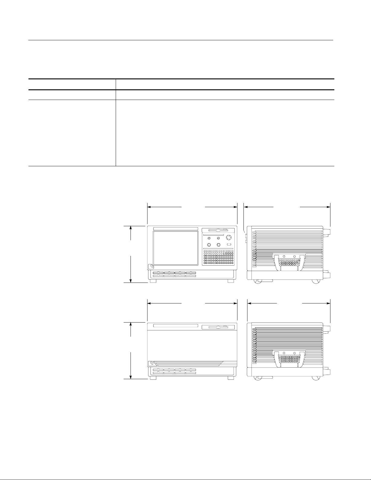
Table 17: TLA600 mechanical characteristics
Characteristic Description
Overall Dimensions See Figure 1 for overall chassis dimensions
Weight Includes empty accessory pouch and front cover
TLA614, TLA624,
18.1 Kg (40 lbs)
TLA613, and TLA623
TLA612, TLA622,
18 Kg (39.75 lbs)
TLA611, and TLA621
TLA604 and TLA603 17.6 Kg (38.75 lbs)
TLA602 and TLA601 17.5 Kg (38.5 lbs)
281.94 mm
(11.10 in)
457.20 mm
(18.00 in)
421.64 mm
(16.60 in)
16
457.20 mm
(18.00 in)
281.94 mm
(11.10 in)
Figure 1: Dimensions of the TLA600 series logic analyzer
TLA Specifications and Characteristics
414.02 mm
(16.30 in)
Page 19

TLA5000 Series Logic Analyzer Specifications
Tables 18 through 32 list the specifications for the TLA5000 series logic
analyzer.
Table 18: TLA5000 input parameters with probes
Characteristic Description
n Threshold Accuracy ±100 mV
Threshold range and step size Settablefrom+4.5Vto--2Vin5mVsteps
Threshold channel selection 16 threshold groups assigned to channels.
P6417, P6418 and P6419 probes have two threshold settings, one for the clock/qualifier channel and one for the data channels.
P6434 probes have four threshold settings, one for each of the clock/qualifier
channels and two for the data channels (one per 16 data channels).
n Channel-to-channel skew ≤ 1 ns maximum
Channel-to-channel skew
(Typical)
Sample uncertainty
Asynchronous: Sample period
Synchronous: 125 ps
Probe input resistance
(Typical)
Probe input capacitance: P6417, P6434
(Typical)
Probe input capacitance: P6418
(Typical)
P6419 input capacitance: P6419
(Typical)
Minimum slew rate
(Typical)
Maximum operating signal 6.0 V
Probe overdrive:
P6417, P6418, P6419
P6434
Maximum nondestructive input signal to probe ±15 V
≤ 0.9 ns
20 kΩ
2pF
1.4 pF data channels
2 pF CLK/Qual channels
<0.7pF
0.2 V/ns
p-p
--3.5 V absolute input voltage minimum
6.5 V absolute input voltage maximum
±250 mV or ±25% of signal swing minimum required beyond threshold, whichever is
greater
±300 mV or ±25% of signal swing minimum required beyond threshold, whichever is
greater
±4 V maximum beyond threshold
Specifications and Characteristics
TLA Specifications and Characteristics
17
Page 20

Specifications and Characteristics
Table 18: TLA5000 input parameters with probes (Cont.)
Characteristic Description
Minimum input pulse width signal
(single channel)
1.5 ns (P6434)
1.25 ns (P6417, P6418, P6419)
(Typical)
Delay time from probe tip to module input
7.33 ns ±100ps
probe connector
(Typical)
Table 19: TLA5000 timing latencies
Characteristic Description
System Trigger and External Signal Input
Latencies
System Trigger and External Signal Output
Latencies (Typical)
1
(Typical)
External System Trigger Input to LA Probe
Tip
External Signal Input to LA Probe Tip via
Signal 3, 4
External Signal Input to LA Probe Tip via
Signal 1, 2
2
--594 ns
--594 ns + Clk
--594 ns + Clk
LA Probe Tip to External System Trigger
3
Out
760 ns + SMPL
LA Probe Tip to External Signal Out via
Signal 3, 4
3
OR function 760 ns + SMPL
AND function 760 ns + SMPL
LA Probe Tip to External Signal Out via
Signal 1, 2
2, 3
normal function 760 ns + SMPL
inverted logic on backplane 760 ns + SMPL
1
All system trigger and external signal input latencies are measured from a falling-edge transition (active true low) with
signals measured in the wired-OR configuration.
2
Signals 1 and 2 (ECLTRG0, 1) are limited to a “broadcast” mode of operation, where only one source is allowed to drive
the signal node at any one time. That single source may be utilized to drive any combination of destinations.
3
SMPL represents the time from the event at the probe tip inputs to the next valid data sample. In the Normal Internal clock
mode, this represents the delta time to the next sample clock. In the MagniVu Internal clock mode, this represents 500 ps
or less. In the External clock mode, this represents the time to the next master clock generated by the setup of the
clocking state machine, the system-under-test supplied clocks, and the qualification data.
18
TLA Specifications and Characteristics
Page 21

Specifications and Characteristics
Table 20: TLA5000 external signal interface
Characteristic Description
System Trigger Input TTL compatible input via rear panel mounted BNC connectors
Input Levels
V
IH
V
IL
Input Mode Falling edge sensitive, latched (active low)
Minimum Pulse Width 12 ns
Active Period Accepts system triggers during valid acquisition periods via real-time gating, resets system
Maximum Input Voltage 0 to +5 V peak
External Signal Input TTL compatible input via rear panel mounted BNC connectors
Input Destination Signal 1, 2, 3, 4
Input Levels
V
IH
V
IL
Input Mode Active (true) low, level sensitive
Input Bandwidth
1
Signal 1, 2, 3, 4 50 MHz square wave minimum
Active Period Accepts signals during valid acquisition periods via real-time gating.
Maximum Input Voltage 0 to +5 V peak
System Trigger Output TTL compatible output via rear panel mounted BNC connectors
Source Mode Active (true) low, falling edge latched
Active Period Outputs system trigger state during valid acquisition period, resets system trigger output to false
Output Levels
V
OH
TTL compatible input
≥ 2.0 V
≤ 0.8 V
trigger input latch between valid acquisition periods.
TTL compatible input
≥ 2.0 V
≤ 0.8 V
state between valid acquisitions.
50 Ω back terminated TTL-compatible output
≥4 V into open circuit
≥ 2Vinto50Ω to ground
V
OL
≤ 0.7Vsinking10mA
Output Protection Short-circuit protected (to ground)
External Signal Output TTL compatible outputs via rear panel mounted BNC connectors
Source Selection Signal 1, 2, 3, 4, or 10 MHz clock
Output Modes
Level Sensitive
Output Levels
V
OH
User definable
Active (true) low or acti ve (true) high
50 Ohm back terminated TTL output
≥ 4 V into open circuit
≥ 2Vinto50Ω to ground
V
OL
Output Bandwidth
1
≤ 0.7Vsinking10mA
Signal 1, 2, 3, 4 50 MHz square wave minimum
TLA Specifications and Characteristics
19
Page 22

Specifications and Characteristics
Table 20: TLA5000 external signal interface (Cont.)
Characteristic Description
Active Period Outputs signals during valid acquisition periods, resets signals to false state between valid
acquisitions.
Outputs 10 MHz clock continuously
Output Protection Short-circuit protected (to ground)
1
The Output Bandwidth specification only applies to signals from the modules; it does not apply to signals applied to the
External Signal Input and sent back to the External Signal Output.
Table 21: TLA5000 channel width and depth
Characteristic Description
Number of channels Product Channels
TLA5201 32 data and 2 clock
TLA5202 64 data and 4 clock
TLA5203 96 data, 4 clock, and 2 qualifier
TLA5204 128 data, 4 clock, and 4 qualifier
Acquisition memory depth Product Memory depth
TLA520X 512 K or optionally either 2 or 8 M samples
1
PowerFlex options
1
20
TLA Specifications and Characteristics
Page 23

Specifications and Characteristics
Table 22: TLA5000 clocking
Characteristic Description
Asynchronous clocking
n Internal sampling period
n Minimum recognizable word
(across all channels)
Synchronous clocking
Number of clock channels
Number of qualifier channels
n Setup and hold window size
(data and qualifiers)
Setup and hold window size
(data and qualifiers)
(Typical)
Setup and hold window range For each channel, the setup and hold window can be moved from +8.0 ns (Ts) to
n Maximum synchronous clock rate 235 MHz in full speed mode (4. 25 ns minimum bet ween active clock edges)
1
500 ps to 50 ms in a 1-2-5 sequence. Storage control can be used to only store data
when it has changed (transitional storage)
2 ns minimum for all channels
1 ns minimum for half channels (using 2:1 demultiplex mode)
0.5 ns minimum for quarter channels (using 4:1 demultiplex mode)
2
Channel-to-channel skew + sample uncertainty
Example: for a P6419, or P6434 Probe anda2nssampleperiod=
1ns+2ns=3ns
3
Product Clock channels
TLA5201 2
TLA5202 4
TLA5203 4
TLA5204 4
4
Product Qualifier channels
TLA5201 0
TLA5202 0
TLA5203 2
TLA5204 4
Maximum window size = Maximum channel-to-channel skew + (2 x sample
uncertainty) + Margin = 1.875 ns
Channel-to-channel skew (typical) + (2 x sample uncertainty) = 1.5 ns
--8.0 ns (Ts) in 0.125 ns steps (setup time). Hold time follows the setup time by the
setup and hold window size.
TLA Specifications and Characteristics
21
Page 24

Specifications and Characteristics
Table 22: TLA5000 clocking (Cont.)
Characteristic Description
2X Demux clocking
TLA5203
TLA5204
TLA5201
TLA5202
Time between Demultiplex clock edges
(Typical)
4X Demux clocking
TLA5203
TLA5204
TLA5201
TLA5202
Time between Demultiplex clock edges
(Typical)
Any individual channel may be demultiplexed wit h it s partner channel. Channels
demultiplex as folllows:
A3(7:0) to/from D3(7:0)
A2(7:0) to/from D2(7:0)
A1(7:0) to/from D1(7:0)
A0(7:0) to/from D0(7:0)
C3(7:0) to/from C1(7:0)
C2(7:0) to/from C0(7:0)
E3(7:0) to/from E1(7:0) TLA5204 only
E2(7:0) to/from E0(7:0) TLA5204 only
CK3 to/from Q2 TLA5204 only
CK2 to/from Q3) TLA5204 only
CK1 to/from Q0
CK0 to/from Q1
Any individual channel may be demultiplexed wit h it s partner channel. Channels
demultiplex as folllows:
A3(7:0) to/from C3(7:0)
A2(7:0) to/from C2(7:0)
A1(7:0) to/from D1(7:0) TLA5202 only
A0(7:0) to/from D0(7:0) TLA5202 only
Same limitations as normal synchronous acquisition
Unlike 2X demultiplexing, the channels within a group of four cannot arbitrarily drive
the others.
E3(7:0) to E2(7:0), E1(7:0), E0(7:0) TLA5204 only
A3(7:0) to A2(7:0), D3(7:0), D2(7:0)
A1(7:0) to A0(7:0), D1(7:0), D0(7:0)
C3(7:0) to C2(7:0), C1(7:0), C0(7:0)
CK3 to CK2, Q3, Q2 TLA5204 only
CK1 to CK0, Q1, Q0
Unlike 2X demultiplexing, the channels within a group of four cannot arbitrarily drive
the others.
A1(7:0) to A0(7:0), D1(7:0), D0(7:0) TL:A5202 only
C3(7:0) to C2(7:0), A3(7:0), A2(7:0)
Same limitations as normal synchronous acquisition
22
TLA Specifications and Characteristics
Page 25

Specifications and Characteristics
Table 22: TLA5000 clocking (Cont.)
Characteristic Description
Clocking state machine
Pipeline delays Each channel can be programmed with a pipeline delay of 0 through 7 active clock
edges.
1
It is possible to use storage control and only store data when it has changed (transitional storage).
2
Applies to asynchronous clocking only. Setup and hold window specification applies to synchronous clocking only.
3
Any or all of the clock channels may be enabled. For an enabled clock channel, either the rising, falling, or both edges
can be selected as the active clock edges. The clock channels are stored.
4
All qualifier channels are stored. For custom clocking there are an additional 4 qualifier channels on C2 3:0 regardless of
channel width.
Table 23: TLA5000 trigger system
Characteristic Description
Triggering Resources
Word/Range recognizers 16 word recognizers. The word recognizers can be combined to form full width, doubl e
bounded, range recognizers. The fol lowing selections are available:
16 word recognizers 0 range recognizers
13 word recognizers 1 range recognizer
10 word recognizers 2 range recognizers
7 word recognizers 3 range recognizers
4 word recognizers 4 range recognizers
Range recognizer channel order From most-significant probe group to least-significant probe group: C3 C2 C1 C0 E3
E2 E1 E0 A3 A2 D3 D2 A1 A0 D1 D0 Q3 Q2 Q1 Q0 CK3 CK2 CK1 CK0
Missing channels for modules with fewer than 136 channels are omitted.
Glitch detector
1,2
Channel groups can be enabled to detect glitches.
Glitches are subject to pulse width variations of up to ±125 ps
Minimum detectable glitch pulse width
(Typical)
Setup and hold violation detector
1,3
1.25 ns (single channel with P6434 probe)
1.0 ns (P6417, P6418, P6419 probe)
Any channel can be enabled to detect a setup or hold violation. The range is from 8.0
ns before the clock edge to 8.0 ns after the clock edge in 0.125 ns steps. The channel
setup and hold violation size can be individually programmed.
The range can be shifted towards the positive region by 0 ns, 4 ns, or 8 ns. With a 0
ns shift, the range is +8 ns to --8 ns; witha4nsshift,therange is +12 ns to --4 ns;
with an 8 ns shift, the range is +16 ns to 0 ns. The sample point selection region is the
same as the setup and hol d window.
TLA Specifications and Characteristics
Any setup value is subject to variation of up to the channel skew specification. Any
hold value is subject to variation of up to the channel skew specification.
23
Page 26

Specifications and Characteristics
Table 23: TLA5000 trigger system (Cont.)
Characteristic Description
Transition detector
Counter/Timers 2 counter/timers, 51 bits wide, can be clocked up to 500 MHz.
External Signal In
External Trigger In A backplane input signal that causes both the main acquisition and the MagniVu
Active trigger resources 16 maximum (excluding counter/timers)
Trigger States 16
n Trigger State sequence rate Same rate as valid data samples received, 500 MHz maximum.
Trigger Machine Actions
Main acquisition trigger Triggers the main acquisition memory.
Main trigger position Trigger position is programmable to any data sample (2 ns boundaries).
MagniVut acquisi tion trigger Triggering of MagniV memory is controlled by t he mai n acquisition trigger machine.
MagniVut trigger position The MagniV trigger position is programmable within 2 ns boundaries and separate
Increment & decrement counter Either of the two counter/timers used as counters can be increased or decreased.
Reloadable word recognizer Loads the current acquired data sample into the reference value of the word
Reloadable word recognizer latency 378 ns
Start/Stop timer Either of the two counter/timers used as timers can be started or stopped.
Reset counter/timer Either of the two counter/timers can be reset.
1
16 transition detectors.
Any channel group can be enabled or disabled to detect a rising transition, a falling
transition, or both rising and falling transitions between the current valid data sample
and the previous valid data sample.
51
Maximum count is 2
Maximum time is 4.5 X 10
-- 1 .
6
seconds or 52 days.
Counters and timers can be set, reset, or tested and have zero reset latency.
1
A backplane input signal.
acquisition to trigger if they are not already triggered.
Word recognizers are traded off one-by-one as External Signal In, glitch detection,
setup and hold detection, or transition detect ion resources are added.
from the main acquisition memory trigger position.
recognizer via a trigger machine action. All data channels are loaded into their
respective word recognizer reference register on a one-to-one manner.
When a counter/timer is used as a timer and is reset, the timer continues from the
started or stopped state that it was in prior to the reset.
Signal out A signal sent to the backplane to be used by other instruments.
Trigger out A trigger out signal sent to t he backplane to trigger other instruments.
24
TLA Specifications and Characteristics
Page 27

Specifications and Characteristics
Table 23: TLA5000 trigger system (Cont.)
Characteristic Description
Storage Control
Global storage Storage is allowed only when a specif ic condition is met. This condition can use any
of the trigger machine resources except for the counter/timers. Storage commands
defined in the current trigger state will override the global storage control.
Global storage can be used to start the acquisition with storage initially turned on
(default) or turned off.
By event Storage can be turned on or off; only the current sample can be stored. The event
storage control overrides any global storage commands.
Block storage When enabled, 31 samples are stored before and after the valid sample.
Not allowed when glitch storage or setup and hold violation is enabled.
Glitch violation storage The acquisition memory can be enabled to store glitch violation information with each
data sample when asynchronous clocking is used. The probe data storage size is
reduced by one half (the other half holds the violation information). The fastest
asynchronous clocking rate is reduced to 4 ns.
Setup and hold violation storage The acquisition memory can be enabled to store setup and hold violation information
with each data sample when synchronous clocki ng is used. The probe data storage
size is reduced by one half (the other half holds the violation information). The
maximum clock rate in this mode is 235 MHz.
1
Each use of External Signal In, glitch detector, setup and hold violation detector, or transition detector requires a trade-off
of one word recognizer resource.
2
Any glitch is subject to pulse width variation of up to the channel-to-channel skew specification + 0.25 ns.
3
Any setup value is subject to variation of up to the channel skew specification. Any hold value is subject to variation of
the channel skew specifications.
TLA Specifications and Characteristics
25
Page 28

Specifications and Characteristics
Table 24: TLA5000 MagniVut feature
Characteristic Description
MagniVu memory depth 16,000 samples per channel
MagniVu sampling period Data is asynchronously sampled and stored every 125 ps in a separate high resolution
memory. The storage speed may be changed (by software) to 250 ps, 500 ps, or
1000 ps so that MagniVu memory covers more time at a lower resolution.
Table 25: TLA5000 Data handling
Characteristic Description
Nonvolatile memory retention time
(Typical)
Battery is integral to the NVRAM. Battery life is > 10 years.
Table 26: TLA5000 internal controller
Characteristic Description
Operating System Microsoft Windows
Microprocessor Intel Celeron, 2 GHz
Main Memory PC2100 DDR SDRAM
Style 184 pin DIMM, 2 Sockets
Speed 100 MHz
Installed configuration 512 MB loaded in one socket
Real-Time Clock and CMOS Setups,
Plug & Play NVRAM Retention Time
Hard Disk Drive Standard PC compatible IDE (Integrated Device Electronics) hard disk drive residing on an
Size Formatted capacity 80 GByte
Battery life is typic ally > 3 years when the logic analyzer is not connected to line voltage. When
connected to line voltage the life of the battery is extended.
Lithium battery, CR2032
EIDE interface.
Continually subject to change due to the fast-moving PC component environment.
These storage capacities valid at product introduction.
CD-RW Drive Standard PC compatible IDE (Integrated Device Electronics)
CD-RWdriveresidingonanEIDEinterface.
Continually subject to change due to the fast-moving PC component environment.
Floppy Disk Drive Standard 3.5 inch 1.44-MB PC compatible high-density, double-sided floppy disk drive.
26
TLA Specifications and Characteristics
Page 29

Specifications and Characteristics
Table 27: TLA5000 display system
Characteristic Description
Classification Standard PC graphics accelerator technology (bitBLT-based); capable of supporting both
internal color LCD display and external color SVGA/XGA monitor.
Display Memory SDRAM-onboard the ATI Mobility I video controller clocked up to 100 MHz.
Size 8 MB
Display Selection Both front panel and external displays can be used simultaneously, each with independent
resolutions. Supports Windows dual-moni tor capability.
External Display Drive Two XGA-compatible analog output ports
Primary Display Size
(RAGE M1 chip)
Secondary Display Size
(845GV chip)
Internal Display
Classification Thin Film Transistor (TFT) 10.4 inch active-matrix color LCD display; CCFL backlight; intensity
Resolution 1024 x 768 pixels
Color Scale 256K
Selected via Windows
Resolution (Pixels) Colors
1024 x 768 256, 64 K, 16.8 M
Selected via Windows
Resolution (Pixels) Colors
640 x 480 256, 64 K, 16.8 M
800 x 600 256, 64 K, 16.8 M
1024 x 768 256, 64 K, 16.8 M
1280 x 1024 256, 64 K, 16.8 M
1600 x 1200 256, 64 K, 16.8 M
1920 x 1440 256, 64K
controllable via software.
Table 28: TLA5000 front-panel interface
Characteristic Description
QWERTY Keypad ASCII keypad to support naming of files, traces, and keyboard equivalents of pointing device
inputs for menus.
Special Function Knobs Various functions
TLA Specifications and Characteristics
27
Page 30

Specifications and Characteristics
Table 29: TLA5000 rear-panel interface
Characteristic Description
Parallel Interface Port (LPT) 25-pin sub-D Parallel Port Connector, Extended Parallel Port (EPP), or Enhanced Capabilities
Port (ECP)
Serial Interface Port (COM 1) 9-pin male sub-D connector to support RS-232 serial port
Two USB Ports Two USB 2.0 (Universal Serial Bus) compliant ports
SVGA Output Ports (SVGA OUT) 15-pin sub-D SVGA connectors (two each, one Primary, one Secondary)
Mouse Port PS/2 compatible mouse port utilizing a mini DIN connector
Keyboard Port PS/2 compatible keyboard port utilizing a mini DIN connector
Table 30: TLA5000 AC power source
Characteristic Description
Source Voltage and Frequency 100--240 VAC ±10%, 47--63 Hz, continuous range CAT II
Maximum Power Consumption 225 Watts line power maximum
Steady-State Input Current 4A
Inrush Surge Current 65 A maximum
Power Factor Correction Yes
On/Standby Switch and Indicator Front Panel On/Standby switch, with indicator.
maximum
RMS
The power cord provides main power disconnect.
Table 31: TLA5000 cooling
Characteristic Description
Cooling System Forced air circulation (negative pressurization) utilizing two fans operating in parallel
Cooling Clearance 51 mm (2 in), sides and rear; unit should be operated on a flat, unobstructed surface
28
TLA Specifications and Characteristics
Page 31

Table 32: TLA5000 mechanical characteristics
Characteristic Description
Overall Dimensions See Figure 1 for overall chassis dimensions
Weight Includes empty accessory pouch and front cover
TLA5201 11.8 Kg (25 lb 15 oz)
TLA5202 11.85 Kg (26 lb 2 oz)
TLA5203 11.9 Kg (26 lb 4 oz)
TLA5204 12Kg (26lb7oz)
Specifications and Characteristics
288.29 mm
(11.350 in)
284.48 mm
(11.200 in)
444.5 mm
(17.500 in)
Figure 2: Dimensions of the TLA5000 series logic analyzer
TLA Specifications and Characteristics
29
Page 32

Specifications and Characteristics
TLA700 System Specifications
Tables 33 through 35 list the specifications common to the TLA715, TLA714,
TLA720, and TLA721 logic analyzers. Detailed specifications for the individual
logic analyzers begin on page 38.
Table 33: TLA700 Backplane interface
Characteristic Description
Slots
Portable mainframe 4
Benchtop mainframe 10 (three slots taken up by the controller module)
Expansion mainframe 13
CLK10 Frequency 10 MHz ±100 PPM
n
Relative Time Correlation Error
TLA7Lx/Mx/Nx/Px/Qx to TLA7Lx/Mx/Nx/Px/Qx “MagniVu” data 2 ns
1,2
(Typical)
TLA7Axx/TLA7NAx to TLA7AxxTLA7NAx “MagniVu” data 2ns
TLA7Axx/TLA7NAx to TLA7Lx/Mx/Nx/Px/Qx “MagniVu” data -- 3 n s
TLA7Lx/Mx/Nx/Px/Qx to TLA7Lx/Mx/Nx/Px/Qx “normal” data using an internal
clock
TLA7Axx/TLA7NAx to TLA7Axx “normal” data using an internal clock 1 TLA7Axx/TLA7NAx sample -- 0.5 ns
TLA7Axx/TLA7NAx to TLA7Lx/Mx/Nx/Px/Qx “normal” data using an internal
clock
TLA7Lx/Mx/Nx/Px/Qx to TLA7Lx/Mx/Nx/Px/Qx “normal” data using an external
clock
TLA7Axx/TLA7NAx to TLA7Axx/TLA7NAx “normal” data using an external
clock
TLA7Axx/TLA7NAx to TLA7Lx/Mx/Nx/Px/Qx “normal” data using an external
clock
1 TLA7Lx/Mx/Nx/Px/Qx sample -- 0.5 ns
1 TLA7Lx/Mx/Nx/Px/Qx sample -- 0.5 ns
2ns
2ns
4ns
30
TLA Specifications and Characteristics
Page 33

Table 33: TLA700 Backplane interface (Cont.)
Characteristic Description
TLA7Lx/Mx/Nx/Px/Qx “MagniVu” to DSO data 3ns
TLA7Axx/TLA7NAx “MagniVu” to DSO data 2ns
TLA7Lx/Mx/Nx/Px/Qx to DSO “normal” data using an internal clock
TLA7Axx/TLA7NAx to DSO “normal” data using an internal clock
TLA7Lx/Mx/Nx/Px/Qx to DSO “normal” data using an external clock
TLA7Axx/TLA7NAx to DSO “normal” data using an external clock
DSO to DSO
1
3
Includes typical jitter, slot-to-slot skew, and probe-to-probe variations to provide a “typical” number for the measurement. Assumes standard accessory probes are utilized.
2
For time intervals longer than 1 s between modules, add 0.01% of the difference between the absolute time
measurements to the relative time correlation error to account for the inaccuracy of the CLK10 source.
3
The DSO module time correlation is measured at the maximum sample rate on one channel only.
3
3
3
3
1 TLA7Lx/Mx/Nx/Px/Qx sample + 2 ns
1 TLA7Axx/TLA7NAx sample + 2 ns
3ns
2ns
3ns
Specifications and Characteristics
TLA Specifications and Characteristics
31
Page 34

Specifications and Characteristics
Table 34: TLA700 Backplane latencies
Characteristic Portable mainframe and
benchtop mainframe
System trigger and external signal input latencies
2
(Typical)
External system trigger input to TLA7Lx/Mx/Nx/Px/ Qx
probe tip
External system trigger input to TLA7Axx probe tip
4
4
External signal input to TLA7Lx/Mx/Nx/Px/Qx probe tip
via Signal 3, 4
5
External signal input to TLA7Axx/TLA7NAx probe tip via
Signal 3, 4
5
External signal input to TLA7Lx/Mx/Nx/Px/Qx probe tip
via Signal 1, 2
5, 6
External signal input to TLA7Axx/TLA7NAx probe tip via
Signal 1, 2
External system trigger input to DSO probe tip
5, 6
4
--266 ns --230 ns
--653 ns --617 ns
--212 ns + Clk --176 ns + Clk
--212 ns + Clk --176 ns + Clk
--634 ns + Clk --596 ns + Clk
--636 ns + Clk --615 ns + Clk
--25 ns 11 ns
System trigger and external signal output latencies1(Typical)
TLA7Lx/Mx/Nx/Px/Qx probe tip to external system trigger
376 ns + SMPL 412 ns + SMPL
out
TLA7Axx/TLA7NAx probe tip to external system trigger
794 ns + SMPL 830 ns + SMPL
out
Expansion
mainframe
TLA7Lx/Mx/Nx/Px/Qx probe tip to external signal out via
Signal 3, 4
3
OR function 366 ns + SMPL 402 ns + SMPL
AND function 379 ns + SMPL 415 ns + SMPL
TLA7Axx/TLA7NAx probe tip to external signal out via
Signal 3, 4
3
OR function 792 ns + SMPL 828 ns + SMPL
AND function 800 ns + SMPL 836 ns + SMPL
TLA7Lx/Mx/Nx/Px/Qx probe tip to external signal out via
Signal 1, 2
3, 6
normal function 364 ns + SMPL 385 ns + SMPL
inverted logic on backplane 364 ns + SMPL 385 ns + SMPL
TLA7Axx/TLA7NAx probe tip to external signal out via
Signal 1, 2
3, 6
normal function 796 ns + SMPL 817 ns + SMPL
inverted logic on backplane 796 ns + SMPL 817 ns + SMPL
32
TLA Specifications and Characteristics
Page 35

Table 34: TLA700 Backplane latencies (Cont.)
Specifications and Characteristics
Characteristic Expansion
Portable mainframe and
benchtop mainframe
mainframe
DSO probe tip to external system trigger out 68 ns 104 ns
DSO Probe tip to external signal out via Signal 3, 4
3
OR function 65 ns 101 ns
AND function 75 ns 111 ns
DSO probe tip to external signal out via Signal 1, 2
3,6
normal function 68 ns 89 ns
inverted logic on backplane 71 ns 92 ns
Inter-module latencies (Typical)
TLA7Lx/Mx/Nx/Px/Qx to DSO inter-module system
1,4
trigger
TLA7Axx/TLA7NAx to DSO inter-module system
1,4
trigger
TLA7Lx/Mx/Nx/Px/Qx to TLA7Lx/Mx/Nx/Px/Qx
inter-module system trigger
1,4
TLA7Axx/TLA7NAx to TLA7Lx/Mx/Nx/Px/Qx inter-module
system trigger
1,4
TLA7Axx/TLA7NAx to TLA7Axx/TLA7NAx inter-module
system trigger
TLA7Lx/Mx/Nx/Px/Qx to DSO inter-module ARM
TLA7Axx/TLA7NAx to DSO inter-module ARM
1,4
1
1
358 ns + SMPL 394 ns + SMPL
772 ns + SMPL 808 ns + SMPL
66 ns + SMPL 102 ns + SMPL
479 ns + SMPL 515 ns + SMPL
116 ns + SMPL 152 ns + SMPL
360 ns + SMPL 396 ns + SMPL
779 ns + SMPL 815 ns + SMPL
TLA7Lx/Mx/Nx/Px/Qx to TLA7Lx/Mx/Nx/Px/Qx
inter-module ARM
1,5
TLA7Axx/TLA7NAx to TLA7Lx/Mx/Nx/Px/Qx inter-module
1,5
ARM
TLA7Axx/TLA7NAx to TLA7Axx inter-module ARM
TLA7Lx/Mx/Nx/Px/Qx to TLA7Lx/Mx/Nx/Px/Qx
inter-module via Signal 1, 2
1,5,6
TLA7Axx/TLA7NAx to TLA7Axx inter-module via Signal
1,5,6
1, 2
TLA7Axx/TLA7NAx to TLA7Lx/Mx/Nx/Px/Qx inter-module
via Signal 1, 2
1,5,6
TLA7Lx/Mx/Nx/Px/Q to TLA7Lx/Mx/Nx/Px/Qx
inter-module via Signal 3, 4
1,5
TLA7AxxTLA7NAx to TLA7Axx inter-module via Signal 3,
1,5
4
TLA Specifications and Characteristics
1,5
108 ns + SMPL + Clk 144 ns + SMPL + Clk
479 ns + SMPL + Clk 533 ns + SMPL + Clk
111 ns + S M PL + Clk 147 ns + SMPL + Clk
116 ns + SMPL + Clk 137 ns + SMPL + Clk
113 ns + SMPL + Clk 134 ns + SMPL + Clk
534 ns + SMPL + Clk 555 ns + SMPL + Clk
116 ns + SMPL + Clk 152 ns + SMPL + Clk
124 ns + SMPL + Clk 160 ns + SMPL + Clk
33
Page 36

Specifications and Characteristics
Table 34: TLA700 Backplane latencies (Cont.)
Characteristic Expansion
TLA7Axx/TLA7NAx to TLA7Lx/Mx/Nx/Px/Qx inter-module
via Signal 3, 4
1,5
TLA7Lx/Mx/Nx/Px/Qx to TLA7Axx/TLA7NAx inter-module
System Trigger
1,4
DSO to TLA7Lx/Mx/Nx/Px/Qx inter-module System
4
Trigger
DSO to TLA7Axx/TLA7NAx inter-module System
4
Trigger
DSO to DSO inter-module System Trigger
4
TLA7Lx/Mx/Nx/Px/Qx to TLA7Axx/TLA7NAx inter-module
1,5
ARM
DSO to TLA7Lx/Mx/Nx/Px/Qx inter-module ARM
DSO to TLA7Axx/TLA7NAx inter-module ARM
5
5
Portable mainframe and
benchtop mainframe
mainframe
545 ns + SMPL + Clk 581 ns + SMPL + Clk
--287 ns + SMPL --251 ns + SMPL
--240 ns --204 ns
--598 ns --562 ns
50 ns 86 ns
--300 ns + SMPL + Clk --264 ns + SMPL + Clk
--192 ns + Clk --156 ns + Clk
--600 ns + Clk --564 ns + Clk
DSO to DSO inter-module ARM 59 ns 95 ns
DSO to TLA7Lx/Mx/Nx/Px/Qx inter-module via
Signal 1, 2
5,6
TLA7Lx/Mx/Nx/Px/Qx to TLA7Axx/TLA7NAx inter-module
via Signal 1, 2
1,5,6
--179 ns + Clk --158 ns + Clk
--294 ns + SMPL + Clk --273 ns + SMPL + Clk
DSO to TLA7Axx/TLA7NAx inter-module via Signal 1,
5,6
2
TLA7Lx/Mx/Nx/Px/Qx to TLA7Axx/TLA7NAx inter-module
via Signal 3, 4
1,5
--598ns + Clk --577 ns + Clk
--294 ns + SMPL + Clk --258 ns + SMPL + Clk
34
TLA Specifications and Characteristics
Page 37

Table 34: TLA700 Backplane latencies (Cont.)
Specifications and Characteristics
Characteristic Expansion
DSO to TLA7Lx/Mx/Nx/Px/Qx inter-module via
Signal 3, 4
5
Portable mainframe and
benchtop mainframe
mainframe
--184 ns + Clk --148 ns + Clk
DSO to TLA7Axx/TLA7NAx inter-module via Signal 3, 45--598 ns + Clk --562 ns + Clk
1
SMPL represents the time from the event at the probe tip inputs to the next valid data sample of the LA module. In the
Normal Internal clock mode, this represents the delta time to the next sample clock. In the Magni Vu Internal clock mode,
this represents 500 ps or less. In the External clock mode, this represents the time to the next master clock generated by
the setup of the clocking state machine, the system-under-test supplied clocks, and the qualification data.
2
All system trigger and external signal input latencies are measured from a falling-edge transition (active true low) with
signals measured in the wired-OR configuration.
3
All signal output latencies are validated to the rising edge of an active (true) high output.
4
In the Waveform window, triggers are always marked immediately except when delayed to the first sample. In the Listing
window, triggers are always marked on the next sample period following their occurrence.
5
“Clk” represents the time to the next master clock at the destin ation logic analyzer. In the asynchronous (or internal)
clock mode, this represents the delta time to the next sample clock beyond the minimum asynchronous rate of 4 ns. In
the synchronous (or external) clock mode, this represents the time to the next master clock generated by the setup of the
clocking state machine and the supplied system under test clocks and qualification data.
6
Signals 1 and 2 are limited to a “broadcast” mode of operation, where only one source is allowed to d rive the signal node
at any one time. That single source may be utilized to drive any combination of destinations.
TLA Specifications and Characteristics
35
Page 38

Specifications and Characteristics
Table 35: TLA700 External signal interface
Characteristic Description
System Trigger Input TTL compatible input via rear panel mounted BNC connectors (portable mainfram e) or front
panel mounted SMB connectors (benchtop mainframe)
Input Levels
V
IH
V
IL
Input destination System trigger
Input Mode Falling edge sensitive, latched (active low)
Minimum Pulse Width 12 ns
Active Period Accepts system triggers during valid acquisition periods via real-time gating, resets system
Maximum Input Voltage 0 to +5 V peak
External Signal Input TTL compatible input via rear panel mounted BNC connectors (portable mainframe) or front
Input Destination Signal 1, 2
Input Levels
V
IH
V
IL
Input Mode Active (true) low, level sensitive
Input Bandwidth
1
Signal 1, 2
Signal 3, 4
Active Period Accepts signals during valid acquisition periods via real-time gating
Maximum Input Voltage 0 to +5 V peak
System Trigger Output TTL compatible output via rear panel mounted BNC connectors (portable mainf rame) or front
Source selection System trigger
Source Mode Active (true) low, falling edge latched
Active Period Outputs system trigger state during valid acquisition period, resets system trigger output to false
Output Levels
V
OH
TTL compatible input
≥ 2.0 V
≤ 0.8 V
trigger input latch between valid acquisition periods
panel mounted SMB connectors (benchtop mainframe)
Signal 3, 4
TTL compatible input
≥ 2.0 V
≤ 0.8 V
50 MHz square w ave minimum
10 MHz square w ave minimum
panel mounted SMB connectors (benchtop mainframe)
state between valid acquisitions
50 Ω back terminated TTL-compatible output
≥4 V into open circuit
≥ 2Vinto50Ω to ground
V
OL
≤ 0.7Vsinking10ma
Output Protection Short-circuit protected (to ground)
36
TLA Specifications and Characteristics
Page 39

Specifications and Characteristics
Table 35: TLA700 External signal interface (Cont.)
Characteristic Description
External Signal Output TTL compatible outputs via rear panel mounted BNC connectors (portable mainframe) or front
panel mounted SMB connectors (benchtop mainframe)
Source Selection Signal 1, 2
Signal 3, 4
10 MHz clock
Output Modes
Level Sensitive
Output Levels
V
OH
User definable
Active (true) low or acti ve (true) high
50 Ω back terminated TTL output
≥ 4 V into open circuit
≥ 2Vinto50Ω to ground
V
OL
Output Bandwidth
Signal 1, 2
Signal 3, 4
2
≤ 0.7Vsinking10ma
50 MHz square w ave minimum
10 MHz square w ave minimum
Active Period Outputs signals during valid acquisition periods, resets signals to false state between valid
acquisitions
Outputs 10 MHz clock continuously
Output Protection Short-circuit protected (to ground)
Intermodule signal line bandwidth Minimum bandwidth up to which the intermodule signals are specified to operate correctly
Signal 1, 2
Signal 3, 4
1
The Input Bandwidth specification only applies to signals to the modules; it does not apply to signals applied to the
50 MHz square w ave minimum
10 MHz square w ave minimum
External Signal Input and sent back to the External Signal Output.
2
The Output Bandwidth specification only applies to signals from the modules; it does not apply to signals applied to the
External Signal Input and sent back to the External Signal Output.
TLA Specifications and Characteristics
37
Page 40

Specifications and Characteristics
TLA715 Dual Monitor Portable Mainframe Characteristics
Tables 36 through 43 describe the specifications for the TLA715 Dual Monitor
Portable Mainframe.
Table 36: TLA715 Internal controller
Characteristic Description
Operating system Microsoft Windows 2000
Microprocessor Intel Pentium PC-AT configuration with an Intel 815E chip-set and a 733 MHz Pentium III
processor
Main memory SDRAM
Style 144 pin SO DIMM, 2 sockets, gold plated, 1.25-inch (3.175 cm) maximum height
Speed 133 MHz
Available configurations 32, 64, 128, 256 MByte per SO DIMM
Installed configurations 512 MB with both sockets loaded
Cache memory 256 KByte Level 2 (L2) write-back cache
Flash BIOS 256 KByte
Real-time clock and CMOS setups
NVRAM
RTC, CMOS setup, & PNP NVRAM
retention time (typical)
Floppy disk drive St andard 3.5 inch 1.44-MB PC compatible high-density, double-sided floppy disk drive,
Bootable replaceable hard disk drive Standard PC compatible IDE (Integrated Device Electronics) hard disk drive resi ding on an
Size 40 GB
Interface ATA --5/enhanced IDE (EIDE)
Average seek time Read, 12 ms
Average latency 7/ 14 ms
I/O data transfer rate 33.3 MBytes/sec maximum (U-DMA mode 2)
Cache buffer 2 MBytes (30 GB) /512 KBytes (10GB)
CD-RW drive Standard PC compatible IDE (Integrated device Electronics) 8x-8x-24x CD-RW drive residing on
Real-time clock/calendar, standard and advanced PC CMOS setups; see BIOS specification
> 10 years bat tery life, lithium battery
500 Kbits/sec transfer rate
EIDE interface.
Continually subject to change due to the fast-moving PC component environment.
These storage capacities valid at product introduction.
an IDE interface.
38
Continually subject to change due to the fast-moving PC component environment.
TLA Specifications and Characteristics
Page 41

Specifications and Characteristics
Table 37: TLA715 display system
Characteristic Description
Classification Standard PC graphics-accelerator technology capable of supporting both internal color LCD
display and two external color VGA, SVGA, or XGA monitors
Display memory 4 MB SDRAM clocked up to 100 MHz, no external video memory
Display selection Hardware sense of external SVGA monitor during BIOS boot sequence; defaults to internal
color LCD display (indicated by two beeps); automatically switches to external SVGA monitor, if
attached (indicated by one beep).
Dual (simultaneous) display of external SVGA monitor and internal color LCD is possible via
special CMOS “simulscan” setup, as long as internal and external displays operate at same
resolution (limited to 800x600 on current LCD) and display rates (simulscan mode indicated by
three beeps).
Four beeps during the BIOS boot indicates a monochrome LCD was found (not supported). Five
beeps indicates no recognizable LCD or external monitor was found.
Dynamic Display Configuration 1 (DDC1) support for external SVGA monitor is provided.
External display drive Two VGA, SVGA, or XGA-compatible analog output ports. Display size is selected via Win2000
display applet.
Display Size
(Primary video port with Silicon
motion chip)
(Secondary video port with 815E
chip set)
Internal display
Classification TFT (Thin Film Transistor) 26 cm active-matrix color LCD displ ay, CCFL backlight, intensity
Resolution 800 X 600, 262, 144 colors with 211.2 mm (8.3 in) by 158.4 mm (6.2 in) of viewing area
Color scale 262, 144 colors (6-bit RGB) with a color gamut of 42% at center to NTSC
Resolution (Pixels
640 x 480 256, 64 K, 16.8 M 60, 75, 85
800 x 600 265, 64 K, 16.8 M 60, 75, 85
1024 x 768 256, 64 K, 16.8 M 60, 75, 85
1280 x 1024 256, 64 K, 16.8 M 60
1600 x 600 256, 64 K 60
1600 x 1200 256, 64 K 60
Resolution (Pixels) Colors Refresh Rates
640 x 480 256, 64 K, 16.8 M 60, 75, 85
800 x 600 256, 64 K, 16.8 M 60, 75, 85
1024 x 768 256, 64 K, 16.8 M 60, 75, 85
1280 x 1024 256, 64 K, 16.8 M 60, 75, 80
1600 x 1200 256 60, 75
controllable via software
) Colors Refresh Rates
TLA Specifications and Characteristics
39
Page 42

Specifications and Characteristics
Table 38: TLA715 front-panel interface
Characteristic Description
QWERTY keypad 31-key ASCII keypad to support naming of files, traces, and keyboard equival ents of pointing
device inputs for menus
HEX keypad 25-key HEX keypad supporting standard DSO and LA entry functions
Special function knobs
Multi-function knob Various increment/decrement functions dependent on screen or window type
Vertical position Scrolling and positioning dependent on display type
Vertical scale Scales waveform displays only
Horizontal position Scrolling and positioning dependent on display type
Horizontal scale Scales waveform displays only
Integrated pointing device Vertically mounted Trackball with two keypad control buttons (SELECT and MENU)
USB port Front panel (lower left-hand side) dual USB connector
Mouse Port PS/2 compatible pointing device port
Keyboard Port PS/2 compatible keyboard port
Table 39: TLA715 rear-panel interface
Characteristic Description
Parallel interface port 36-pin high-density connector supports Output only, Enhanced Parallel Port (EPP), or Microsoft
high-speed mode (ECP)
Complies with IEEE P1284-C/D2 for bi-directional Parallel Peripheral Interface for Personal
Computers (draft) style 1284-C
Serial interface port 9-pin male sub-D connector to support RS-232 serial port
SVGA output Port 1 and Port 2 Two 15-pin sub-D SVGA connectors
PC CardBus32 port Standard Type I, II, III PC-compatible, PC card slot
Complies with PCMCIA 2.1 and JEIDA 4.1
40
TLA Specifications and Characteristics
Page 43

Table 40: TLA715 AC power source
(
,
v
a
geava
(CombinedSystem,voltageavail-
Characteristic Description
Source voltage and frequency 90 V
Fuse rating
100 V
RMS
RMS
to 250 V
to 132 V
, 45 Hz to 66 Hz, continuous range CAT II;
RMS
, 360 Hz to 440 Hz, continuous range CAT II
RMS
Specifications and Characteristics
90 V to 250 V operation
(159--0046--00)
90 V to 250 V operation
(159--0381--00)
UL198/CSA C22.2
0.25 in × 1.25 in, Fast Blow, 8 A, 250 V
IEC 127/Sheet 1
5mm× 20 mm, Fast Blow, 6.3 A, 250 V
Maximum power consumption 600 W
Steady-state input current 6A
maximum at 90 VAC
RMS
, 60 Hz or 100 VAC
RMS
RMS
, 400 Hz
Inrush surge current 70 A maximum
Power factor correction Yes
On/Sleep indicator Green/yellow front panel LED located next to On/Standby switch provides visual feedback when
the On/Off switch is actuated. When the LED is green, the instrument is powered and the
processor is not sleeping. When the LED is yellow, the instrument is powered, but the processor
is sleeping.
On/Standby switch and indicator Front panel On/Standby switch. Users can push the switch to power down the instrument
without going through the Windows shutdown process; the instrument normally powers down.
The power cord provides main power disconnect.
Table 41: TLA715 secondary power
Characteristic Description
n DC Voltage Regulation Voltage Minimum Nominal Maximum
Combined System
able at each slot)
olt
+24 V
il-
+12 V
+5 V
-- 2 V
-- 5 . 2 V
-- 1 2 V
23.28 V 24.24 V 25.20 V
11.64 V 12.12 V 12.60 V
4.875 V 5.063 V 5.250 V
--2.10 V --2.00 V --1.90 V
--5.460 V --5.252 V --5.044 V
--12.60 V --12.12 V --11.64 V
-- 2 4 V --25.20 V --24.24 V --23.28 V
TLA Specifications and Characteristics
41
Page 44

Specifications and Characteristics
Table 42: TLA715 cooling
Characteristic Description
Cooling system Forced air circulation system with no removable filters using six fans operating in parallel
Pressurization Negative pressurization system in all chambers including modules
Slot activation Installing a module activates the cooling for the corresponding occupied slots by opening the
airflow shutter mechanism. Optimizes cooling efficiency by only applying airflow to installed
modules.
Air intake Front sides and bottom
Air exhaust Back rear
Cooling clearance 2 inches (51 mm) front, sides, top, and rear. Prevent blockage of airflow to bottom of instrument
by placing on a solid, noncompressable surface; can be operated on rear feet.
Fan speed and operation All fans operational at half their rated potential and speed (12 VDC)
Table 43: TLA715 mechanical
Characteristic Description
Overall dimensions (See Figure 4 for overall chassis di mensions) Dimensions are without front feet extended, front
cover attached, pouch attached, nor power cord attached.
Height (with feet) 9.25 in (23.5 cm)
Width 17 in (43.18 cm)
Depth 17.5 in (44.45 cm)
Weight 30 lbs 12 oz (13.9 kg) with no modules installed, two dual-wide slot covers, and empty pouch
Shipping configuration 60 lbs 13 oz (27.58 kg) minimum confi gurat ion (no modules), with all standard accessories
86 lbs 9 oz (39.26 kg) full configuration, with two TLA 7P4 modules and standard accessories
(including probes and clips)
Acoustic noise level (typical) 42.7 dBA weighted (operator)
37.0 dBA weighted (bystander)
Construction materials Chassis parts are constructed of aluminum alloy; front panel and trim peaces are constructed of
plastic; circuit boards are constructed of glass.
Finish type Tektronix blue body and Tektronix silver-gray trim and front with black pouch, FDD feet, handle,
and miscellaneous trim pieces
42
TLA Specifications and Characteristics
Page 45

Specifications and Characteristics
17 in
(43.18 cm)
9.25 in
(23.5 cm)
Figure 3: Dimensions of TLA715 portable mainframe
17.5 in
(44.45 cm)
TLA Specifications and Characteristics
43
Page 46

Specifications and Characteristics
TLA714 Portable Mainframe Characteristics
Tables 44 through 51 describe the specifications for the TLA714 Portable
Mainframe.
Table 44: TLA714 Internal controller
Characteristic Description
Operating System Microsoft Windows
Microprocessor Intel Pentium PC-AT configuration with a 266 MHz Intel Pentium MMX microprocessor
Main Memory SDRAM
Style 144 pin SO DIMM, 2 Sockets
Speed 66 MHz
Installed Configurations Minimum 64 MB loaded in one socket
Maximum 128 MB with both sockets loaded
Cache Memory 512 KB Level 2 (L2) write-back cache
Flash BIOS 512 KB
Provides PC plug-and-play servi ces wit h and without
Microsoft Windows operating system.
Flash based BIOS field upgradable via a fl oppy disk.
Real-Time Clock and CMOS Setups
NVRAM
Bootable Replaceable Hard Disk
Drive
Size Minimum 10 GByte
Interface ATA 4/Enhanced IDE (EIDE)
Average seek time Read 13 ms
I/O data-transfer rate 33.3 MB/s max (U-DMA mode 2) (ATA33)
CD-RW Drive Standard PC compatible IDE (Integrated device Electronics) 8x-8x-24x CD-RW drive residing on
Floppy Disk Drive Standard 3.5 inch 1.44-MB PC compatible high-density, double-sided floppy disk drive
Real-Time clock/calendar, with typical 10-year life. Standard and advanced PC CMOS setups.
Standard PC compatible IDE (Integrated device Electronics) hard disk drive residing on an EIDE
interface.
Maximum 30 GByte
Continually subject to change due to the fast-moving PC component environment.
These storage capacities valid at product introduction.
an IDE interface
Continually subject to change due to the fast-moving PC component environment
44
TLA Specifications and Characteristics
Page 47

Specifications and Characteristics
Table 45: TLA714 display system
Characteristic Description
Classification Standard PC graphics accelerator technology (bitBLT-based); capable of supporting both
internal color LCD display and external color SVGA/XGA monitor
Display Memory DRAM-based frame-buffer memory
Size 2 MB
Display Selection Hardware sense of external SVGA monitor during BIOS boot sequence; defaults to internal
color LCD display; automatically switches to external SVGA monitor, if attached
Dual (simultaneous) display of external SVGA monitor and internal color LCD is possible via
special “simulscan” CMOS setup, as long as internal and external displays operate at same
resolution (limited to 800x600 on current TFT LCD) and display rates
Dynamic Display Configuration (DDC2 A and B) support for external SVGA monitor is provided.
External Display Drive One SVGA/XGA-compatible analog output port
Display Size User selected via Microsoft Windows
Plug and Play support for DDC1 and DDC2 A and B
Resolution (Pixels) Colors
640 x 480 256
640 x 480 64,000
640 x 480 16,800,000
800 x 600 256
800 x 600 64,000
800 x 600 16,800,000
1024 x 768 256
1280 x 1024 256
1600 x 1200 256
Internal Display
Classification Thin Film Transistor (TFT) 10.4 inch active-matrix color LCD display; CCFL backlight; intensity
controllable via software
Resolution 800 x 600 pixels
Color Scale 262,144 colors (6-bit RGB)
TLA Specifications and Characteristics
45
Page 48

Specifications and Characteristics
Table 46: TLA714 front-panel interface
Characteristic Description
QWERTY Keypad ASCII keypad to support naming of files, traces, and keyboard equivalents of pointing device
inputs for menus
HEX Keypad HEX keypad supporting text entry f unctions
Special Function Knobs Various functions
Integrated Pointing Device GlidePoint touchpad
Dual USB Ports Two USB (Universal Serial Bus) compliant ports
Mouse Port PS/2 compatible mouse port utilizing a mini DIN connector
Keyboard Port PS/2 compatible keyboard port utilizing a mini DIN connector
Table 47: TLA714 rear-panel interface
Characteristic Description
Parallel Interface Port (LPT) 36-pin high-density connector supports standard Centronics mode, Enhanced Parallel Port
(EPP), or Microsoft high-speed mode (ECP)
Serial Interface Port (COM A) 9-pin male sub-D connector to support RS-232 serial port
SVGA Output Port (SVGA OUT) 15-pin sub-D SVGA connector
Type I and II PC Card Port Standard Type I and II PC-compatible PC card slot
Type I, II, and III PC Card Port Standard Type I, II , and III PC-compatible PC card slot
Table 48: TLA714 AC power source
Characteristic Description
Source Voltage and Frequency 90--250 V
100--132 V
Fuse Rating
90 V - 250 V Operation
(159-0046-00)
90 V - 250 V Operation
(159-0381-00)
UL198/CSA C22.2
0.25 in × 1.25 in, Fast Blow, 8 A, 250 V
IEC 127/Sheet 1
5mm× 20 mm, Fast Blow, 6.3 A, 250 V
Maximum Power Consumption 600 W line power m aximum
Steady-State Input Current 6A
RMS
Inrush Surge Current 70 A maximum
45--66 Hz, continuous range CAT II
RMS,
360--440 Hz, continuous range CAT II
RMS,
maximum
46
TLA Specifications and Characteristics
Page 49

Specifications and Characteristics
(
,
v
a
geava
(CombinedSystem,voltageavail-
Table 48: TLA714 AC power source (Cont.)
Characteristic Description
Power Factor Correction Yes
On/Standby Switch and Indicator Front Panel On/Standby switch, with LED indicator located next to switch
The power cord provides main power disconnect.
Table 49: TLA714 secondary power
Characteristic Description
n DC Voltage Regulation Voltage Minimum Nominal Maximum
Combined System
able at each slot)
olt
+24 V 23.28 V 24.24 V 25.20 V
il-
+12 V
+5 V
-- 2 V
-- 5 . 2 V
-- 1 2 V
-- 2 4 V --25.20 V --24.24 V --23.28 V
11.64 V 12.12 V 12.60 V
4.875 V 5.063 V 5.250 V
--2.10 V --2.00 V --1.90 V
--5.460 V --5.252 V --5.044 V
--12.60 V --12.12 V --11.64 V
Table 50: TLA714 cooling
Characteristic Description
Cooling System Forced air circulation (negative pressurization) utilizing six fans operating in parallel
Cooling Clearance 2 in (51 mm), sides and rear; unit should be operated on a flat, unobstructed surface
Slot Activation Installing a module activates the cooling for the corresponding occupied slots by opening the air flow
shutter mechanism. Optimizes cooling efficiency by only applying airflow to modules that are
installed.
TLA Specifications and Characteristics
47
Page 50

Specifications and Characteristics
Table 51: TLA714 mechanical
Characteristic Description
Overall Dimensions (See Figure 4 for overall chassis dimensions.)
Height (with feet) 9.25 i n (235 mm)
Width 17.0 in (432 mm)
Depth 17.5 in (445 mm)
Weight
(Typical)
Shipping configuration
(Typical)
9.25 in
(23.5 cm)
30 lbs 12 oz. (13.9 kg) with no modules installed, 2 dual-wide slot covers, and empty pouch
88 lbs (26.3 kg) mi nimum configuration (no modules or probes), with all standard accessories
87 lb (39.5 kg) full configuration, with 2 TLA7P4 modules and standard accessories (including
probes)
17 in
(43.18 cm)
17.5 in
(44.45 cm)
Figure 4: Dimensions of TLA714 portable mainframe
48
TLA Specifications and Characteristics
Page 51

Specifications and Characteristics
Benchtop and Expansion Mainframe Characteristics
Tables 52 through 56 list the specifications for the TLA720/721 Benchtop
mainframe and the TLA7XM expansion mainframe.
Table 52: Benchtop and expansion mainframe AC power source
Characteristic Description
Source Voltage 90--250 V
100--132 V
Maximum Power Consumption 1450 W line power (the maximum power consumed by a fully loaded 13-slot
instrument)
Fuse Rating
(Current and voltage ratings and type of fuse
used to fuse the source line voltage)
45--66 Hz, continuous range CAT II
RMS,
360--440 Hz, continuous range CAT II
RMS,
90 V -- 132 VAC
High-power/Low Line (159-0379-00)
RMS
Operation
Safety: UL198G/CSA C22.2
Size: 0.25 in × 1.25 in
Style: Slow acting
Rating: 20 A/250 V
103 V -- 250 VAC
(159-0256-00)
RMS
Operation
Safety: UL198G/CSA C22.2
Size: 0.25 in × 1.25 in
Style: No. 59/Fast acting
Rating: 15 A/250 V
207 V -- 250 VAC
(159-0381-00)
RMS
Operation
Safety: IEC 127/Sheet 1
Size: 5 mm × 20 mm
Style: Fast acting “F”, high-breaking capacity
Rating: 6.3 A/250 V
Inrush Surge Current 70 A maximum
Steady State Input Current 16.5 A
6.3 A
maximum at 90 VAC
RMS
maximum at 207 VAC
RMS
RMS
RMS
Power Factor Correction (Typical) 0.99 at 60 Hz operation and 0.95 at 400 Hz operation
ON/Standby Switch and Indicator Front Panel On/Standby switch with integral power indicator
TLA Specifications and Characteristics
49
Page 52

Specifications and Characteristics
(
,
v
a
geava
(CombinedSystem,voltageavail-
Table 53: Benchtop and expansion mainframe secondary power
Characteristic Description
n DC Voltage Regulation Voltage Minimum Nominal Maximum
Combined System
able at each slot)
olt
+24 V 23.28 V 24.24 V 25.20 V
il-
+12 V
+5 V
-- 2 V
-- 5 . 2 V
-- 1 2 V
-- 2 4 V --25.20 V --24.24 V --23.28 V
11.64 V 12.12 V 12.60 V
4.875 V 5.063 V 5.250 V
--2.10 V --2.00 V --1.90 V
--5.460 V --5.252 V --5.044 V
--12.60 V --12.12 V --11.64 V
Table 54: Benchtop and expansion mainframe cooling
Characteristic Description
Cooling system Forced air circulation system (positi v e pressurization) using a single low-noise
centripetal (squirrel cage) fan configuration with no filters for the power supply and 13
module slots.
Fan speed control Rear panel switch selects between full speed and variable speed. Sl ot exhaust
temperature and ambient air temperature are monitored such that a constant delta
temperature is maintained.
Slot activation Installing a module activates the cooling for the corresponding occupied slots by opening
the air flow shutter mechanism. Optimizes cooling efficiency by only applying airflow to
modules that are installed.
Pressurization Positive pressurization system, all chambers including modules
Slot airflow direction P2 to P1, bottom of module to top of module
Mainframe air intake Lower fan-pack rear face and bottom
Mainframe air exhaust Top-sides and top-rear back. Top rear-back exhaust redirected to the sides by the fan
pack housing to minimize reentry into the intake.
∆ Temperature readout sensitivity 100 mV/ °Cwith0°C corresponding to 0 V output
Temperature sense range -- 1 0 °Cto+90°C, delta temperature ≤ 50 °C
Clearance 2 in (51 mm), rear, top, and sides
Fan speed readout RPM = 20 ¢ (Tach frequency) or 10 (+Pulse Width)
where (+Pulse Width) is the positive width of the TACH1 fan output signal measured
in seconds
Fan speed range 650 to 2250 RPM
50
TLA Specifications and Characteristics
Page 53

Specifications and Characteristics
Table 55: Enhanced monitor
Characteristic Description
Voltage readout +24 V, --24 V, +12 V, --12 V, +5 V, --5.2 V, --2 V, +5 V
present, and +5 V
External
via RS232
Voltage readout accuracy (Typical) ±3% maximum
Current readout Readout of the present current on the +24 V, --24 V, +12 V,
--12 V, +5 V, --2 V, --5.2 V rails via RS232
Standby
if
Current readout accuracy (Typical) ±5% of maximum power supply I
mp
Rear panel connector levels ±25 VDC maximum, 1 A maximum per pin
(Provides access for RS-232 host to enhanced monitor)
Table 56: Benchtop and expansion mainframe mechanical
Characteristic Description
Overall Dimensions (See Figures 5 and 6 for overall dimensions.)
Standard
Height (with feet) 13.7 in (346.7 mm) including feet
Width 16.7 in (424.2 mm)
Depth 26.5 in (673.1 mm)
Rackmount
Height 13.25 in (336.6 mm)
Width 18.9 in (480.1 mm)
Depth 28.9 in to 33.9 i n (734.1 mm to 861.1 mm) in 0.5 in increments, user selectable
Benchtop controller dimensions
Height 10.32 in (262.1 mm)
Width 2.39 in (60.7 mm)
Depth 14.75 in (373.4 mm)
Expansion module dimensions
Height 10.32 in (262.1 mm)
Width 1.25 in (31.75 mm)
Depth 14.75 in (373.4 mm)
Weight
Mainframe with benchtop controller and
58 lbs 11 oz. (26.7 kg)
slot fillers
(Typical)
TLA Specifications and Characteristics
51
Page 54

Specifications and Characteristics
Table 56: Benchtop and expansion mainframe mechanical (Cont.)
Characteristic Description
Shipping configuration
(Typical)
Benchtop controller 6 lbs 10 oz. (3.0 kg)
Expansion module 3 lbs (1.4 kg)
Maximum per slot 5lbs(2.27kg)
Rackmount kit adder 20 lbs (9.1 kg)
Size
Benchtop controller Three slots wide
Expansion module Single slot wide
60 lbs 11 oz. (26.7 kg) minimum configuration with controller (only) and all standard
accessories (two manuals, five dual-wide and one singl e-wi de slot filler panels, power
cord, empty pouch, front cover, keyboard, software, and cables)
187 lbs (85 kg) full y confi gured,
same as above with the addition of five LA modules (four TLA7P4 modules, one
TLA7N4 module) and all modul e standard accessories (probes and clips)
Acoustic noise level (Typical)
Variable fan speed (at 860 RPM) 43.2 dBA weighted (front)
43.8 dBA weighted (back)
Full speed fan (switched at rear) 66.2 dBA weighted (front)
66.2 dBA weighted (back)
Construction materials Chassis parts, aluminum alloy
Front panel and trim pieces, plastic
Circuit boards, glass laminate
Finish type Mainframes are Tektronix silver gray with dark gray trim on fan pack and bottom feet
support rails.
Benchtop controllers are Tektronix silver gray on front lexan and injector/ejector
assemblies with a black FDD and PC card ejector buttons.
52
TLA Specifications and Characteristics
Page 55

Specifications and Characteristics
16.7 in
(42.4 cm)
13.7 in
(35 cm)
13.3 in
(34 cm)
Figure 5: Dimensions of the benchtop and expansion mainframe
18.9 in
(48 cm)
26.5 in
(67 cm)
28.9in(73.4cm)Minto
33.9 in (86.1 cm) Max
13.25 in
(33.66 cm)
Figure 6: Dimensions of the benchtop and expansion mainframe with rackmount option
TLA Specifications and Characteristics
53
Page 56

Specifications and Characteristics
TLA721 Dual Monitor Benchtop Controller Characteristics
Tables 57 and 58 lists the specifications for the TLA721 Dual Monitor Benchtop
Controller.
Table 57: TLA721 benchtop controller characteristics
Characteristic Description
Operating system Microsoft Windows 2000
Microprocessor Intel 733 MHz Pentium III configuration with an Intel 815E chip-set
Main memory Two 144 pin SODIMM sockets support one or two SDRAM modules.
Available configurations 16, 32, 64, 256 MB per SODIMM
Installed configuration 512 MB maximum configuration
Speed 133 MHz
CAS latency 2, 3
RAS to CAS delay 2, 3
RAS precharge 2, 3
DRAM cycle time 5/7 or 7/9
Cache memory 512 KB, level 2 (L2) write-back cache
Flash BIOS 512 KB
Provides PC plug-and-play servi ces wit h and without
Microsoft Windows operating system.
Flash based BIOS field upgradable via a fl oppy disk
Forced recovery jumper is provided
Real-time clock and CMOS setups NVRAM Real-time clock/calendar. Standard and advanced PC CMOS setups: see BIOS
specifications
RTC, CMOS setup, & PnP NVRAM retention
time (Typical)
Floppy disk drive Standard 3.5 inch, 1.44 MB, high-density, double-sided, PC-compatible high-density
Transfer rate 500 Kbits per second
Access time (ave.) 194 ms
Bootable replaceable hard disk drive Standard PC compatible IDE (Integrated device Electronics) hard disk drive residing
Size 40 GByte
Battery life is typically > 7 years
floppy disk drive
on an EIDE interface
Continually subject to change due to the fast-moving PC component environment.
These storage capacities valid at product introduction.
Interface ATA-5/Enhanced IDE (EIDE)
54
TLA Specifications and Characteristics
Page 57

Specifications and Characteristics
Table 57: TLA721 benchtop controller characteristics (Cont.)
Characteristic Description
Average seek time Read 12 ms
I/O data-transfer rate 33.3 MB/s maximum (U-DMA mode 2)
Average latency 7/14 ms
Cache buffer 512 KB
CD-RW Drive Standard PC compatible IDE (Integrated device Electronics) 8x-8x-24x CD-RW drive
residing on an IDE interface.
Continually subject to change due to the fast-moving PC component environment.
Applicable formats CD-DA; CE-ROM Mode 1, Mode 2; CD-ROM XA Mode 2 (Form 1, Form 2); Photo CD
(single/multi session); Enhanced CD
Interface IDE (ATAPI)
Average access time 130 ms
Data-transfer rate (burst sust ained) 16.7 MB per second maximum, 1290--3000 KB per second
TLA Specifications and Characteristics
55
Page 58

Specifications and Characteristics
Table 57: TLA721 benchtop controller characteristics (Cont.)
Characteristic Description
Display classification Standard PC graphics accelerator technology (bitBLT based) residing on the
Peripheral Component Interconnect (PCI) bus capable of supporting external color
VGA, SVGA, or XGA monitors
Display configuration Hardware automatically senses a missing flat panel LCD in the benchtop mainframe
and defaults to the external SVGA monitor output during the BIOS boot sequence (no
internal TFT LCD display exists). This is indicated by a single beep during the boot
sequence.
Dynamic Display Configuration 1 (DDC1) support for the external monitor is provided.
Display memory 4 MB SDRAM is on board the video controller; no external video memory
Display drive Two VGA, SVGA, or XGA compatible analog output ports
Display size User selected via Microsoft Windows
Plug and Play support for DDC1 and DDC2 A and B
(Primary video port with Silicon Motion Chip)
Resolution (Pixels) Colors Refresh Rates
640 x 480 256, 64 K, 16.8 M
60, 75, 85
800 x 600 256, 64 K, 16.8 M
60, 75, 85
1024 x768 256, 64 K, 16.8 M 60, 75, 85
1280 x 1024 256, 64 K, 16.8 M 60
1600 x 600 256, 64 K 60
1600 x 1200 256, 64 K 60
(Secondary video port with 815E Chip set)
Resolution (Pixels) Colors Refresh Rates
640 x 480 256, 64 K, 16.8 M
60, 75, 85
800 x 600 256, 64 K, 16.8 M
60, 75, 85
1024 x768 256, 64 K, 16.8 M 60, 75, 85
1280 x 1024 256, 64 K, 16.8 M 60, 75, 85
1600 x 1200 256 60, 75
Table 58: Front panel characteristics
Characteristic Description
SVGA output port (SVGA) Two 15-pin sub-D SVGA connectors
Dual USB ports Two USB (Universal Serial Bus) compliant ports
Mouse port Front panel mounted PS2 compatible mouse port utilizing a mini DIN connector
Keyboard port Front panel mounted PS2 compatible keyboard port utilizing a mini DIN connector
56
TLA Specifications and Characteristics
Page 59

Specifications and Characteristics
Table 58: Front panel characteristics (Cont.)
Characteristic Description
Parallel interface port (LPT) 36-pin high-density connector supports standard Centronics mode, Enhanced Parallel
Port (EPP), or Microsof t high-speed mode (ECP)
Serial interface port (COM) 9-pin male sub-D connector to support an RS232 serial port
PC CardBus32 port Standard Type I and II PC compatible PC card slot
Type I, II, and III PC Card Port Standard Type I, II, and III PC compatible PC card slot
TLA Specifications and Characteristics
57
Page 60

Specifications and Characteristics
TLA720 Benchtop Controller Characteristics
Tables 59 through 60 list the specifications for the TLA720 Benchtop Controller.
Table 59: TLA720 benchtop controller characteristics
Characteristic Description
Operating System Microsoft Windows
Microprocessor Intel Pentium 266 MHz PC-AT configuration with an Intel chip-set
Main Memory SDRAM
Style Two 144 pin SODIMM sockets support one or two SDRAM modules.
Installed Configuration 128 MB
Two 64 MB SDRAM modules installed
Speed 60 ns
Cache Memory 256 K, level 2 (L2) write-back cache
Flash BIOS 512 KB
Provides PC plug-and-play servi ces wit h and without
Microsoft Windows operating system.
Flash based BIOS field upgradable via a fl oppy disk
Real-Time Clock and CMOS Setups NVRAM
(Typical)
Floppy Disk Drive Standard 3.5 inch, 1.44 MB, double-sided, PC-compatible high-density floppy disk
Bootable Replaceable Hard Disk Drive Standard PC compatible IDE (Integrated device Electronics) hard disk drive residing
Size Maximum 30 GByte
Interface ATA-4/Enhanced IDE (EIDE)
Average seek time Read 13 ms
I/O data-transfer rate 33.3 MB/s maximum (U-DMA mode 2)
CD-RW Drive Standard PC compatible IDE (Integrated device Electronics) 8x-8x-24x CD-RW drive
Real-time clock/calendar, with typical 7-year life. Standard and advanced PC CMOS
setups: see BIOS specification.
drive
on an EIDE interface
Continually subject to change due to the fast-moving PC component environment.
These storage capacities valid at product introduction.
residing on an IDE interface.
Continually subject to change due to the fast-moving PC component environment.
58
TLA Specifications and Characteristics
Page 61

Specifications and Characteristics
Table 59: TLA720 benchtop controller characteristics (Cont.)
Characteristic Description
Display Classification Standard PC graphics accelerator technology (bitBLT based) capable of driving
external color VGA, SVGA, or XGA monitors
Display Memory DRAM based frame-buffer memory
Size 2MB
Display Drive One VGA, SVGA, or XGA compatible analog output port
Display Size User selected via Microsoft Windows
Plug and Play support for DDC1 and DDC2 A and B
Resolution (Pixels) Colors
640 x 480 256
640 x 480 64,000
640 x 480 16,800,000
800 x 600 256
800 x 600 64,000
800 x 600 16,800,000
1024 x768 256
1280 x 1024 256
1600 x 1200 256
SVGA Output Port (SVGA) The SVGA port utilizing a 15-pin sub-D SVGA connector
Dual USB Ports Two USB (Universal Serial Bus) compliant ports
Mouse Port Front panel mounted PS2 compatible mouse port utilizing a mini DIN connector
Keyboard Port Front panel mounted PS2 compatible keyboard port utilizing a mini DIN connector
Parallel Interface Port (LPT) 36-pin high-density connector supports standard Centronics mode, Enhanced Parallel
Port (EPP), or Microsof t high-speed mode (ECP)
Serial Interface Port (COM) 9-pin male sub-D connector to support an RS232 serial port
Type I and II PC Card Port Standard Type I and II PC compatible PC card slot
Type I, II, and III PC Card Port Standard Type I, II, and III PC compatible PC card slot
Table 60: TLA720 benchtop controller mechanical characteristics
Characteristic Description
Weight (Typical) 6 lb. 10 oz. (2.9 kg)
Size Three slots wide
Overall dimensions
Height 10.32 in (262 mm)
Width 3.6 in (83 mm)
Depth 14.7 in (373 mm)
TLA Specifications and Characteristics
59
Page 62

Specifications and Characteristics
TLA7Axx/TLANAx Series Logic Analyzer Module Characteristics
Tables 61 though 69 list the specifications of the TLA7Axx/TLA7NAx Series
Logic Analyzer modules.
Table 61: TLA7Axx/TLA7NAx input parameters (with probes)
Characteristic Description
n Threshold accuracy
(Certifiable parameter)
Threshold range and step size Setable from +4.5 V to --2.0 V in 5 mV steps
Threshold channel selection 16 threshold groups assigned to channels. Each probe has four t hreshold sett ings,
n Channel to channel skew
Channel to channel skew (Typical)
Sample uncertainty
Asynchronous Sample period
Synchronous 125 ps
Minimum slew rate (Typical) 0.2 V/ns
Input voltage range -- 2 . 5 V t o + 5 V
Maximum operating voltage swing 6.0 V peak-to-peak
Probe overdrive
Single ended probes
Differential probes
Maximum nondestructive input signal to probe
Minimum input pulse width (single channel)
(Typical)
P6860, P6880, P6960, and P6980 probes 500 ps
P6810 probes 750 ps
±(35 mV + 1% of the threshold voltage setting)
one for each of t he clock/qualifier channels and one per group of 16 data channels.
≤400 ps maximum
When merged, add the following for slave modules:
0.0 ns when data is acquired on the slave modules through local clocks
125 ps when data is acquired on the slave modules via the master modules’clock
and merge deskew has been performed.
375 ps when data is acquired on the slave modules via the master module’sclock
and merge deskew has NOT been performed.
≤300 ps
When merged, add the following for slave modules:
0.0 ns when data is acquired on the slave modules through local clocks
125 ps when data is acquired on the slave modules via the master modules’clock
and merge deskew has been performed.
375 ps when data is acquired on the slave modules via the master module’sclock
and merge deskew has NOT been performed.
±150 mV or ±25% of signal swing minimum required beyond threshold, whichever
one is greater
V
-- V
pos
±15 V
is ≥ 150mV
neg
p-p
60
TLA Specifications and Characteristics
Page 63

Specifications and Characteristics
Table 61: TLA7Axx/TLA7NAx input parameters (with probes) (Cont.)
Characteristic Description
Delay time from probe tip to input probe
connector (Typical)
P6860, P6960, and P6980 probes
P6810 and P6880 probes
7.7 ns ± 60 ps
7.7 ns ± 80 ps
Table 62: TLA7Axx analog output
Characteristic Description
Number of outputs Four analog outputs regardless of the module channel width. Any four of the module’s
channels can be mapped to the four analog outputs.
Attenuation 10X mode for normal operation
5X mode for small signals (--1.5 V to +2.5 V)
Bandwidth (Typical) 2GHz
Accuracy (gain and offset)
(Typical)
±(50 mV + 2% of signal amplitude)
Table 63: Channel width and depth
Characteristic Description
Number of channels
TLA7AA4, TLA7AB4, TLA7NA4 128 data, 8 clock/qualifier
TLA7AA3, TLA7NA3 96 data, 6 clock/qualifier
TLA7AA2, TLA7AB2, TLA7NA2 64 data, 4 clock/qualifier
TLA7AA1, TLA7NA1 32 data, 2 clock/qualifier
Acquisition memory depth
TLA7AAx, TLA7NAx series 32 M per channel, maximum
TLA7ABx series 64 M per channel, maximum
TLA Specifications and Characteristics
61
Page 64

Specifications and Characteristics
M
a
c
lockcha
2
ProductC
lockcha
M
lavec
lockcha
2
ProductC
lockcha
g
(
c
a
Qualifiercha
3
ProductQualifiercha
Table 64: Clocking
Characteristic Description
Asynchronous clocking
n Internal sampling period 500 ps to 50 ms in a 1--2--5 sequence. Storage control can be used to only store data
when it has changed (transitional storage)
2 ns minimum for all channels
1 ns minimum for half channels (using 2:1 Demultiplex mode)
0.5 ns minimum for quarter channels (using 4:1 Demultiplex mode)
n Minimum recognizable word
(across all channels)
Synchronous clocking
ster
ergeds
nnels
nnels
1
Channel-to-channel skew + sample uncertainty
Example for a P6860 high-density probe anda2nssampleperiod:
400 ps + 2 ns = 2.4 ns
nnels
32+2 module 2
64+4 module 4
96+6 module 4
128+8 module 4
nnels
(64+4 channel modules and 32+2 channel
modules
nnot be merged.)
nnels
Single channel setup and hold window size
(Typical)
n Single module setup and hold window
size (data and qualifiers)
Single module setup and hold window size
(data and qualifiers) (Typical)
96+6 module 4
128+8 module
4
nnels
32+2 module 0
64+4 module 0
96+6 module 2
128+8 module 4
500 ps
Maximum window size = Maximum channel-to-channel skew + (2 x sample
uncertainty) + 100 ps
Maximum setup time = User interface setup time + 75 ps
Maximum hold time = User interface hold time + 50 ps
Example using P6810, P6860, or P6880 probe and user interface setup and hold of
625/0 typical:
Maximum window size = 400 ps + 250 ps + 100 ps = 750 ps
Maximum setup time = 625 ps + 75 ps = 700 ps
Maximum hold time = 0.0 ps + 50 ps = 50 ps
Typical window size = Typical channel-to-channel skew + (2 x sample
uncertainty) + 75 ps
Example using P6860 probe: 300 ps + 250 ps + 75 ps = 625 ps
62
TLA Specifications and Characteristics
Page 65

Table 64: Clocking (Cont.)
Characteristic Description
Specifications and Characteristics
Merged module setup and hold window size
(data and qualifiers) (Typical)
Maximum window size = Single module setup and hold + merge skew
When determining the required setup and hold window for merged modules, take into
consideration if the slave module’s local clocks are used to acquire data and if a
merge deskew has been performed. If the slave module uses its own clocks to
acquire data, then the typical and maximum setup and hold values are the same as a
stand-alone module (the same is true for the master module itself). The only time the
additional merge skew values apply is when the clocks on the master module acquire
data on the slave modules.
When a slave module acquires data using its own local clocks, merge skew = 0 ps
When a slave module acquires data using clocks from the master module without
merge deskew, merge skew = 375 ps
When a slave module acquires data using clocks from the master module and has
had merge deskew performed, merge skew = 125 ps.
Example using P6810, P6860, or P6880 probe with slave module acquiring data via
clocks from the master module without merge deskew:
Maximum window size = 750 ps + 375 ps =1.125 ns
Typical window size = 625 ps + 375 ps = 1.000 ns
The user interface setup and hold window for merge applications is affected as follows
by merge skew:
Typical setup time = User interface setup time + (merge skew/2)
Typical hold time = User interface hold time + (merge skew/2)
Maximum setup time = User interface setup time + 75 ps + (merge skew/2)
Maximum hold time = User interface hold time + 50 ps + (merge skew/2)
Example using P6810, P6860, or P6880 probe, with user interface default setup and
hold time of 625/0 typical, and merge configuration that has had merge deskew
performed:
Typical setup time = 625 ps + (125 ps/2) = 688 ps
Typical hold time = 0 ps + (125 ps/2) = 62 ps
Maximum setup time = 625 ps + 75 ps + (125 ps/2) = 763 ps
Maximum hold time = 0 ps + 50 ps + (125 ps/2) = 112 ps
Setup and hold window range For each channel, the setup and hold window can be moved from +8.0 ns (Tstypical)
to --8.0 ns (T
typical) in 0.125 ns steps (setup time).
s
The setup and hold window can be shifted toward the setup region by 0 ns, 4 ns, or
8ns.Witha0nsshift,therange is +8 ns to --8 ns; witha4nsshift,therange is
+12 ns to --4 ns; with an 8 ns shift, the range is +16 ns to 0 ns. The sample point
selection region is the same setup and hold window. Setup times are specified as
typical figures. Hold time follows the setup time by the setup and hold window size.
n Maximum synchronous clock rate
TLA7Axx series
450 MHz in full-speed mode (2.2 ns mini mum between active clock edges)
235 MHz in half-speed mode (4.25 ns minim um between acti ve clock edges)
TLA Specifications and Characteristics
120 MHz in quarter-speed mode (8.3 ns minimum between active clock edges)
800 MHz on half channels
4
Software controls the selection between full-speed and half-speed modes.
63
Page 66

Specifications and Characteristics
TLA7N
A
TLA7AA3,TLA7AA4,TLA7AB4,TLA7NA3
A7NA
TLA7NA4module
s
Table 64: Clocking (Cont.)
Characteristic Description
n Maximum synchronous clock rate
TLA7NAx series
Demultiplex clocking (two clock edges required)
Demultiplex channels (2:1)
TLA7AA3, TLA7AA4, TLA7AB4, TLA7NA3,
4modules
TLA7AA1, TLA7AA2, TLA7AB2, TLA7NA1,
TLA7NA2 modules
Demultiplex channels (4:1)
TL
TLA7AA1, TLA7AA2, TLA7AB2, modules Unlike the 2:1 Demultiplex, the channels within a group of four cannot arbitrarily drive
4 modules
450 MHz in full-speed mode (2.2 ns mini mum between active clock edges)
235 MHz in full-speed mode (4.25 ns mini mum between active clock edges)
Software controls the selection between full-speed and half-speed modes.
Any individual channel can be demultiplexed with its partner channel. If multiplexing is
enabled, all of the A and D channels are multiplexed; there is no individual selection.
Channels demultiplex as follows:
A3(7:0) to/from D3(7:0)
A2(7:0) to/from D2(7:0)
A1(7:0) to/from D1(7:0)
A0(7:0) to/from D0(7:0)
E3(7:0) to/from E1(7:0) TLA7AA4, TLA7AB4, and TLA7NA4 only
E2(7:0) to/from E0(7:0) TLA7AA4, TLA7AB4, and TLA7NA4 only
CK3 to/from Q2 TLA7AA4, TLA7AB4, and TLA7NA4 only
CK2 to/from Q3 TLA7AA4, TLA7AB4, and TLA7NA4 only
CK2 to/from Q3
CK2 to/from Q3
Any individual channel can be demultiplexed with its partner channel. If multiplexing is
enabled, all of the A and D channels are multiplexed; there is no individual selection.
Channels demultiplex as follows:
A3(7:0) to/from C3(7:0)
A2(7:0) to/from C2(7:0)
A1(7:0) to/from D1(7:0) TLA7AA2, TLA7NA2, TLA7NA2 modules only
A0(7:0) to/from D0(7:0) TLA7AA2, TLA7NA2, TLA7NA2 modules only
Unlike the 2:1 Demultiplex, the channels within a group of four cannot arbitrarily drive
the others.
,
E3(7:0) to E2(7:0), E1(7:0), E0(7:0) TLA7AA4, TLA7AB4 modules only
A3(7:0) to A2(7:0), D3(7:0), D2(7:0)
A1(7:0) to A0(7:0), D1(7:0), D0(7:0)
C3(7:0) to C2(7:0), C1(7:0), C0(7:0)
CK3 to CK2, Q3, Q2 TLA7AA4, TLA7AB4, modules only
CK1 to CK0, Q1, Q0
the others.
A1(7:0) to A0(7:0), D1(7:0), D0(7:0) TLA7AA2, TLA7AB2, only
C3(7:0) to C2(7:0), A3(7:0), A2(7:0)
64
TLA Specifications and Characteristics
Page 67

Table 64: Clocking (Cont.)
Characteristic Description
Specifications and Characteristics
Time between Demultiplex clock edges
Same limitations as normal synchronous acquisition
(Typical)
Source synchronous clocking (TLA7Axx)
Clocks per module Four
Clocks with merged modules When merged, the slave modules have two clocks available from the master module.
Including the local clocks, the total is six clocks.
Clock groups Four for a single module and for a merged system
Size of clock group valid FIFO Four stages when operated at 235 MHz or below (three stages when operated above
235 MHz); this allows four (source synchronous or other) clocks to occur before the
clock that completes the Clock Group Valid signal for that group.
Source synchronous clock alignment window Channel-to-channel skew only
Source synchronous clock reset The Clock Group Valid FIFO can be reset in one of the t wo ways:
1. By the overflow of a presettable (0--255) 8-bit counter that counts one of the
following clocks: 2 ns Clock or the master heartbeat clock (synchronous or
asynchronous). An active edge places the reset count to its preset value. An active
clock edge will clear the Clock Group Valid reset before the clock gets to the FIFO so
that no data is lost.
2. By enabling an external reset. I n this mode, one of the clock channels must be
traded on the master module to act as a level-sensitive reset input. Any one of the
clocks can be selected. A polarity selection is available. This mode affects all Clock
Group Complete circuits.
Neither one of the above m odes can be intermixed; one or the other must be
selected.
Clocking state machine
Pipeline delays Channel groups can be programmed with a pipeline delay of 0 through 7 active clock
changes.
1
Specification only applies with asynchronous (internal) clocking. With synchronous clocking, the setup and hold window
size applies.
2
Any or all clock channels can be enabled. For an enabled clock channel, either the rising, falling, or both edges can be
selected as active clock edges. Clock channels are stored.
3
Qualifier channels are stored.
4
This is a special mode and has some limitations such as the clocking state machine and trigger state machine only
running at 500 MHz.
TLA Specifications and Characteristics
65
Page 68

Specifications and Characteristics
Table 65: TLA7Axx/TLA7NAx module trigger system
Characteristic Description
Trigger resources
Word recognizers and range recognizers 16, word recognizers can be combined to form full width, double bounded range
recognizers. The following selections are available:
16 word recognizers 0 range recognizers
13 word recognizers 1 range recognizer
10 word recognizers 2 range recognizers
7 word recognizers 3 range recognizers
4 word recognizers 4 range recognizers
Range recognizer channel order From most-significant probe group to least-significant probe group:
C3 C2 C1 C0 E3 E2 E1 E0 A3 A2 D3 D2 A1 A0 D1 D0 Q3 Q2 Q1 Q0 CK3 CK2 CK1
CK0
Missing channels for modules with fewer than 136 channels are omitted. When
merged, the range recognition extends across the modules. The master module
contains the most-significant groups.
Glitch detector
(normal asynchronous clock mode)
Minimum detectable glitch pulse width
(Typical)
Setup and hold violation detector
(normal synchronous clock mode)
Channel groups can be enabled to detect glitches.
Glitches are subject to pulse width variations of up to ±125 ps
Minimum input pulse width (single channel)
P6860, P6960 high density probe: 500 ps
P6880, P6980 differential probe: 500 ps
P6810 general purpose probe: 750 ps
Any channel can be enabled to detect a setup or hold violation. The range is from
8.0 ns before the clock edge to 8.0 ns after the clock edge in 0.125 ns steps. The
channel setup and hold violation size can be individually programmed.
The range can be shifted towards the positive region by 0 ns, 4 ns, or 8 ns. With a
0 ns shift, the range is +8 ns to --8 ns; witha4nsshift,therange is +12 ns to --4 ns;
with an 8 ns shift, the range is +16 ns to 0 ns. The sample point selection region is the
same as the setup and hol d window.
Any setup value is subject to variation of up to the channel skew specification. Any
hold value is subject to variation of up to the channel skew specification.
Transition detector 16 transition detectors.
Any channel group can be enabled or disabled to detect a rising transition, a falling
transition, or both rising and falling transitions between the current valid data sample
and the previous valid data sample.
Counter/timers 2 counter/timers, 51 bits wide, can be clocked up to 500 MHz
Maximum count is 2^50--1 (excluding sign bit)
Maximum time is 4.5 × 10
Counters can be used as setable, resettable, and testable flags. Counters can be
reset, do nothing, increased, or decreased. Timers can be reset, started, stopped, or
not changed. Counters and timers have zero reset latency and one clock terminal
count latency.
66
6
seconds or 52 days
TLA Specifications and Characteristics
Page 69

Specifications and Characteristics
Table 65: TLA7Axx/TLA7NAx module trigger system (Cont.)
Characteristic Description
Signal In 1 A backplane input signal.
Signal In 2 A backplane input signal.
Trigger In A backplane input signal that causes the main acquisition and the MagniVu
acquisition to trigger if they are not already triggered.
Active trigger resources 16 maximum (excluding counter/timers)
Word recognizers are traded off one-for-one as Signal In 1, Signal In 2, glitch
detection, setup and hold detection, or transition detection resources are added.
Trigger states 16
n Trigger state sequence rate Same rate as valid data samples received. 500 MHz maximum.
Trigger machine actions
Main acquisition trigger Triggers the main acquisition memory
Main trigger position Programmable to any data sample (2 ns boundaries)
MagniVu trigger Main acquisition machine controls the triggering of the MagniVu memory
MagniVu trigger position Programmable within 2 ns boundaries and separate from the main acquisition
memory trigger position
Increment/decrement counter Counter/timers used as counters can be increased or decreased.
Start/stop timer Either of the two counter/timers used as timers can be started or stopped.
Reset counter/timer Either of the two counter/timers can be reset.
When a counter/timer used as a timer is reset, the timer continues in the started or
stopped state that it was prior to the reset.
Reloadable word recognizer (snapshot) Loads the current acquired data sample into the reference value of the word
recognizer via a trigger machine action. All data channels are loaded into their
respective word recognizer reference register on a one-to-one manner.
Reloadable word recognizer latency 378 ns
Signal Out A signal sent to the backplane to be used by other modules
Trigger Out A signal sent to the backplane to trigger other modules
Storage control
Storage Storage is allowed only if a specific condition is met. The condition can use any of the
trigger resources except for counter/timers. Storage commands defined in the current
trigger state will override the global storage control.
Storage can be used to start the acquisition with storage initially turned on (default
setting) or off.
By event Storage can be turned on or off; only the current sample can be stored. Event storage
control overrides any global storage commands.
TLA Specifications and Characteristics
67
Page 70

Specifications and Characteristics
Table 65: TLA7Axx/TLA7NAx module trigger system (Cont.)
Characteristic Description
Block storage (store stretch) When enabled, 31 samples are stored before and after the valid sample.
This allows the storage of a group of samples around a valid data sample when
storage control is being used. This only has meaning when storage control is used.
Block storage is disallowed when glitch storage or setup and hold violation storage is
enabled.
Glitch violation storage Glitch violation information can be stored to acquisition memory with each data
sample when asynchronous clocking is used. The acquisit ion data storage size is
reduced by half when t his mode is enabled (the other half holds violation information).
The fastest asynchronous clock rate is reduced to 4 ns.
Setup and hold violation storage Setup and hold violation information can be stored to acquisition memory with each
data sample when synchronous clocking is used. The acquisition data storage size is
reduced by half when t his mode is enabled (the other half holds violation information).
The maximum synchronous clock rate in this mode is 235 MHz.
Table 66: MagniVu acquisition
Characteristic Description
MagniVu sampling period Data is asynchronously sampled and stored every 125 ps in a separate MagniVu
(high-resolution) memory. The storage speed can be changed by software to 250 ps,
500 ps, or 1000 ps with no loss in memory depth s o that the high resolution memory
covers more time at a lower resolution.
MagniVu memory depth Approximately 16 K per channel. The MagniVu memory is separate from the main
acquisition memory.
Table 67: Merged modules
Characteristic Description
Number of merged modules 2, 3, 4, or 5 adjacent modules can be merged. Only 102-channel modules or
136-channel modules can be merged. Merged modules can have unequal channel
widths and channel depths.
Number of channels after merging The sum of all channels available on each of the merged modules including clocks
and qualifiers. No channels are lost when modules are merged.
Merged system acquisition depth Channel depth is equal to that of the shallowest module.
Number of clock and qualifier channels after
merging
The qualifier channels on the slave modules can only be used as data channels. They
cannot influence the actual clocking function of the logic analyzer (for example, log
strobe generation).
68
The clock channels on the slave TLA7Axx modules can capture data on those
modules for source-synchronous applications. Each slave module contribut es four
additional clock channels to the merged set. All clock and qualifier channels are
stored to acquisition memory.
TLA Specifications and Characteristics
Page 71

Specifications and Characteristics
Table 67: Merged modules (Cont.)
Characteristic Description
Merged system trigger resources The same as a single module except for word recognizer width, setup and hold
violation detector width, glitch detector width, and transition detector width has
increased to equal that of the merged channel width. Range recognizers will increase
to the merged channel width up to three modules; range recognition is not supported
on the two outside slave modules.
Merged range significance Most significant Master, Slave 1, Slave 2
Table 68: Data handling
Characteristic Description
Nonvolatile memory retention time (Typical) The battery life is integral to the NVRAM; battery life is > 10 years.
Table 69: Mechanical
Characteristic Description
Material Chassis parts are constructed of aluminum alloy. The front panel is constructed of
plastic laminated to steel front panel. Circuit boards are constructed of glass laminate.
Weight
136-channel module 5lb6oz.(2.438kg)
102-channel module 5 lb 4 oz. (2.381 kg)
68-channel module 5 lb 0.5 oz. (2.282 kg)
34-channel module 4 lb 15.5 oz. (2.254 kg)
Shipping weight 7 lb 12 oz. (3.515 kg) for 136-channel module when packaged for domestic shipment
Overall dimensions
Height 10.32 in (262 mm)
Width 2.39 in (61 mm) with merge connector in the recessed position
Width increases by 0.41 in (10.41 m m) with merge connector in the extended position
Length 14.7 in (373 mm)
Mainframe interlock 1.4 ECL keying is implemented
TLA Specifications and Characteristics
69
Page 72

Specifications and Characteristics
TLA7Lx/Mx/Nx/Px/Qx Module Characteristics
Tables 70 through 76 list the specifications of the TLALx/Mx/Nx/Px/Qx logic
analyzer modules.
Table 70: LA module channel width and depth
Characteristic Description
Number of channels Product Channels
TLA7N1, TLA7L1, TLA7M1 32 data and 2 clock
TLA7N2, TLA7P2, TLA7Q2, TLA7L2, TLA7M2 64 data and 4 clock
TLA7N3, TLA7L3, TLA7M3 96 data, 4 clock, and 2 qualifier
TLA7N4, TLA7P4, TLA7Q4, TLA7L4, TLA7M4 128 data, 4 clock, and 4 qualifier
Acquisition memory depth Product Memory depth
TLA7L1, TLA7L2, TLA7L3, TLA7L4 32 K or 128 K samples
TLA7M1, TLA7M2, TLA7M3, TLA7M4 512 K samples
TLA7N1, TLA7N2, TLA7N3, TLA7N4 64 K or 256 K or 1 M or 4 M samples
TLA7P2, TLA7P4 16 M samples
TLA7Q2, TLAQP4 64 M samples
1
PowerFlex options
1
1
Table 71: LA module clocking
Characteristic Description
Asynchronous clocking
n Internal sampling period
n Minimum recognizable word
(across all channels)
Synchronous clocking
Number of clock channels
1
4 ns to 50 ms in a 1--2--5 sequence
2 ns in 2x Clocking mode
2
Channel-to-channel skew + sample uncertainty
Example: for a P6417 or a P6418 Probe anda4nssampleperiod=
3
Product Clock channels
TLA7N1, TLA7L1, TLA7M1 2
TLA7N2, TLA7P2, TLA7Q2, TLA7L2, TLA7M2 4
TLA7N3, TLA7L3, TLA7M3 4
TLA7N4, TLA7P4, TLA7Q4, TLA7L4, TLA7M4 4
1.6ns+4ns=5.6ns
70
TLA Specifications and Characteristics
Page 73

Specifications and Characteristics
Table 71: LA module clocking (Cont.)
Characteristic Description
Number of qualifier channels Product Qualifier channels
TLA7N1, TLA7L1, TLA7M1 0
TLA7N2, TLA7P2, TLA7Q2, TLA7L2, TLA7M2 0
TLA7N3, TLA7L3, TLA7M3 2
TLA7N4, TLA7P4, TLA7Q4, TLA7L4, TLA7M4 4
n Setup and hold window size
(data and qualifiers)
Setup and hold window size
(data and qualifiers)
(Typical)
Setup and hold window range For the TLA7Nx/Px/Qx logic analyzer modules, each channel of the setup and hold
Maximum window size = Maximum channel-to-channel skew + (2 x sample
uncertainty) + 0.4 ns
Maximum setup time = User interface setup time + 0.8 ns
Maximum hold time = User interface hold time + 0.2 ns
Maximum setup time for slave module of merged pair =
User Interface setup time + 0.8 ns
Maximum hold time for slave module of merged pair =
User Interface hold time + 0.7 ns
Examples: for a P6417, P6418, or P6434 probe and user interface
setup and hold of 2.0/0.0 typical:
Maximum window size = 1.6 ns + (2 x 500 ps) + 0.4ns = 3.0 ns
Maximum setup time = 2.0 ns + 0.8 ns = 2.8 ns
Maximum hold time = 0.0 ns + 0.2 ns = 0.2ns
Channel-to-channel skew (typical) + (2 x sample uncertainty)
Example: for P6417 or P6418 Probe = 1 ns + (2 x 500 ps) = 2 ns
window can be moved from +8.5 ns (Ts) to --7.0 ns (Ts) in 0.5 ns steps (setup time).
Hold time follows the setup time by the setup and hold window size.
n Maximum synchronous clock rate
4
Demux clocking
Demux Channels
TLA7N3, TLA7N4, TLA7P4, TLA7Q4,
TLA 7L3, TLA 7L4, TLA 7M3, TLA 7M4
TLA7N1, TLA7N2, TLA7P2, TLA7Q2,
TLA 7L1, TLA 7L2, TLA 7M1, TLA 7M2
Time between DeMux clock edges
4
(Typical)
TLA Specifications and Characteristics
For the TLA7Lx and TLAMx logic analyzer modules, the user interface restricts the
setup and hold window range to groups rather than individual channels.
200 MHz in full speed mode (5 ns minimum between active clock edges)
100 MHz in half speed mode (10 ns minimum between active clock edges)
Channels multiplex as follows:
A3(7:0) to D3(7:0)
A2(7:0) to D2(7:0)
A1(7:0) to D1(7:0)
A0(7:0) to D0(7:0)
Channels multiplex as follows:
A3(7:0) to C3(7:0)
A2(7:0) to C2(7:0)
A1(7:0) to D1(7:0) TLA7N2, TLA7P2, TLA7Q2, TLA 7L2, TLA 7M2 only
A0(7:0) to D0(7:0) TLA7N2, TLA7P2, TLA7Q2, TLA 7L2, TLA 7M2 only
5 ns minimum between DeMux clock edges in full-speed mode
10 ns minimum between DeMux clock edges in half-speed mode
71
Page 74

Specifications and Characteristics
Table 71: LA module clocking (Cont.)
Characteristic Description
Time between DeMux store clock edges
(Typical)
Data Rate (Typical)
TLA7N1, TLA7N2, TLA7P2, TLA7Q2,
TLA7N3, TLA7N4, TLA7P4, TLA7Q4,
Clocking state machine
Pipeline delays For the TLA7Nx/Px/Qx logi c analyzer modules, each channel can be programmed
1
It is possible to use storage control and only store data when it has changed (transitional storage).
2
Applies to asynchronous clocking only. Setup and hold window specification applies to synchronous clocking only.
3
Any or all of the clock channels may be enabled. For an enabled clock channel, the rising edge, falling edge, or both
edges can be selected as the active clock edges. The clock channels are stored.
4
Full and half speed modes are controlled by PowerFlex options and upgrade kits.
4
10 ns minimum between DeMux master clock edges in full-speed mode
20 ns minimum between DeMux master clock edges in half-speed mode
400 MHz (200 MHz option required) half channel.
(Requires channels to be multiplexed.)
These multiplexed channels double the memory depth.
with a pipeline delay of 0 through 3 active clock edges.
For the TLA7Lx and TLAMx logic analyzer modules, the user interface restricts the
programming to groups rather than individual channels.
Table 72: LA module trigger system
Characteristic Description
Triggering Resources
Word/Range recognizers 16 word recognizers. The word recognizers can be combined to form full width, doubl e
bounded, range recognizers. The fol lowing selections are available:
16 word recognizers 0 range recognizers
13 word recognizers 1 range recognizer
10 word recognizers 2 range recognizers
7 word recognizers 3 range recognizers
4 word recognizers 4 range recognizers
Range recognizer channel order From most-significant probe group to least-significant probe group: C3 C2 C1 C0 E3
E2 E1 E0 A3 A2 D3 D2 A1 A0 D1 D0 Q3 Q2 Q1 Q0 CK3 CK2 CK1 CK0
Missing channels for modules with fewer than 136 channels are omitted. When
merged, the range recognition extends across all the modules; the master module
contains the most-significant groups.
The master module is to the left (lower--numbered slot) of a merged pair.
The master module is in the center when three modules are merged. Slave module 1
is located to the right of the master module, and slave module 2 is located to the left
of the master module.
Glitch detector
1,2
Each channel group can be enabled to detect a glitch
72
TLA Specifications and Characteristics
Page 75

Table 72: LA module trigger system (Cont.)
Characteristic Description
Specifications and Characteristics
Minimum detectable glitch pulse width
2.0 ns (single channel with a P6417, P6418, or P6434 probe)
(Typical)
Setup and hold violation detector
1,3
Each channel can be enabled to detect a setup and hold violation. The range is from
8 ns before the clock edge to 8 ns after the cl ock edge. The range can be selected in
0.5 ns increments.
For the TLA7Lx and TLAMx logic analyzer modules, the user interface restricts the
setup and hold violation detector to groups rather than individual channels.
The setup and hold violation of each window can be individually programmed.
Transition detector
1, 4
Each channel group can be enabled or disabled to detect a transition between the
current valid data sample and the previous valid data sample.
Counter/Timers 2 counter/timers, 51 bits wide, can be clocked up to 250 MHz.
Maximum count is 2
Maximum time is 9.007 X 10
51
.
6
seconds or 104 days.
Counters and timers can be set, reset, or tested and have zero reset latency.
Signal In 1 A backplane input signal
Signal In 2 A backplane input signal
Trigger In A backplane input signal that causes the main acquisition and the MagniVut
acquisition to trigger if they are not already triggered
Active trigger resources 16 maximum (excluding counter/timers)
Word recognizers are traded off one-by-one as Signal In 1, Signal In 2, glitch
detection, setup and hold detection, or transition detection resources are added.
Trigger States 16
n Trigger State sequence rate Same rate as valid data samples received, 250 MHz maximum
Trigger Machine Actions
Main acquisition trigger Triggers the main acquisition memory
Main trigger position Trigger position is programmable to any data sample (4 ns boundaries)
Increment counter Either of the two counter/timers used as counters can be increased.
Start/Stop timer Either of the two counter/timers used as timers can be started or stopped.
Reset counter/timer Either of the two counter/timers can be reset.
When a counter/timer is used as a timer and is reset, the timer continues in the
started or stopped state that it was in prior to the reset.
Signal out A signal sent to the backplane to be used by other modules
Trigger out A trigger out signal sent to the backplane to trigger other modules
TLA Specifications and Characteristics
73
Page 76

Specifications and Characteristics
Table 72: LA module trigger system (Cont.)
Characteristic Description
Storage Control
Global storage Storage is allowed only when a specif ic condition is met. This condition can use any
of the trigger machine resources except for the counter/timers. Storage commands
defined in the current trigger state will override the global storage control.
Global storage can be used to start the acquisition with storage initially turned on
(default) or turned off.
By event Storage can be turned on or off; only the current sample can be stored. The event
storage control overrides any global storage commands.
Block storage When enabled, 31 samples are stored before and after the valid sample.
Block storage is disallowed when glitch storage or setup and hold violation is enabled.
Glitch violation storage The acquisition memory can be enabled to store glitch violation information with each
data sample when asynchronous clocking is used. The probe data storage size is
reduced by one half (the other half holds the violation information). The fastest
asynchronous clocking rate is reduced to 10 ns.
1
Each use of a glitch detector, setup and hold violation detector, or transition detector requires a trade-off of one word
recognizer resource.
2
Any glitch is subject to pulse width variation of up to the channel-to-channel skew specification + 0.5 ns.
3
For TLA7N1, TLA7N2, TLA7N3, TLA7N4, TLA7P2, TLA7P4, TLA7Q2, and TLA7Q4 Logic Analyzer modules, any setup
value is subject to variation of up to 1.8 ns; any hold value is subject to variation of up to 1.2 ns. For TLA7L1, TLA7L2,
TLA7L3, TLA7L4, TLA7M1, TLA7M2, TLA7M3, and TLA7M4 Logic Analyzer modules, any setup value is subject to
variation of up to 1.6 ns; any hold value is subject to variation of up to 1.4 ns.
4
This mode can be used to create transitional storage selections where all channels are enabled.
Table 73: LA module MagniVut feature
Characteristic Description
MagniVut mem ory depth 2016 samples per channel
MagniVut sampling period Data is asynchronously sampled and stored every 500 ps in a separate high resolution
memory.
Table 74: LA module data handling
Characteristic Description
Nonvolatile memory retention time
(Typical)
74
Battery is integral to the NVRAM. Battery life is > 10 years.
TLA Specifications and Characteristics
Page 77

Specifications and Characteristics
Table 75: LA module input parameters with probes
Characteristic Description
n Threshold Accuracy ±100 mV
Threshold range and step size Settable from +5 V to --2 V in 50 mV steps
Threshold channel selection 16 threshold groups assigned to channels.
P6417 and P6418 probes have two threshold settings, one for the clock/qualifier
channel and one for the data channels.
P6434 probes have four threshold settings, one for each of the clock/qualifier
channels and two for the data channels (one per 16 data channels).
n Channel-to-channel skew ≤ 1.6 ns maximum (When merged, add 0.5 ns for the slave module.)
Channel-to-channel skew
(Typical)
Sample uncertainty
Asynchronous: Sample period
Synchronous: 500 ps
Probe input resistance
(Typical)
Probe input capacitance: P6417, P6434
(Typical)
Probe input capacitance: P6418
(Typical)
Minimum slew rate
(Typical)
Maximum operating signal 6.5 V
Probe overdrive:
P6417, P6418
P6434
Maximum nondestructive input signal to probe ±15 V
Minimum input pulse width signal
(single channel)
(Typical)
Delay time from probe tip to input probe
connector
(Typical)
≤ 1.0 ns typical (When merged, add 0.3 ns for the slave module.)
20 kΩ
2pF
1.4 pF data channels
2 pF CLK/Qual channels
0.2 V/ns
p-p
--3.5 V absolute input voltage minimum
6.5 V absolute input voltage maximum
±250 mV or ±25% of signal swing minimum required beyond threshold, whichever is
greater
±300 mV or ±25% of signal swing minimum required beyond threshold, whichever is
greater
±4 V maximum beyond threshold
2ns
7.33 ns
TLA Specifications and Characteristics
75
Page 78

Specifications and Characteristics
Table 76: LA module mechanical
Characteristic Description
Slot width Requires 2 mainframe slots
Weight
(Typical)
Overall dimensions
Height 262 mm (10.32 in)
Width 61 mm (2.39 in)
Depth 373 mm (14.7 in)
Probe cables
P6417 length 1.8 m (6 ft)
P6418 length 1.93 m (6 ft 4 in)
P6434 length 1.6 m (5 ft 2 in)
Mainframe interlock 1.4 ECL keying is implemented
5 lbs 10 oz. (2.55 kg) for TLA7N4 and TLA7P4
8 lbs (3.63 kg) for TLA7N4 and TLA7P4 packaged for domestic shipping
76
TLA Specifications and Characteristics
Page 79

DSO Module Characteristics
n
Tables 77 through 81 list the specifications for the DSO Module.
Table 77: DSO module signal acquisition system
Characteristic Description
n Accuracy, DC gain ±1.5% for full scale ranges from 20 mV to 100 V
±2.0% for full scale ranges <19.9 mV
n Accuracy, i nternal offset
1
Full scale range setting Offset accuracy
Specifications and Characteristics
10 mV -- 1 V
1.01 V -- 10 V
10.1 V -- 100 V
Analog bandwidth, DC--50 Ω coupled Full scale range setting Bandwidth
10.1 V -- 100 V DC -- 500 MHz (TLA7E1 and TLA7E2)
100 mV -- 10 V DC -- 1 GHz (TLA7E1 and TLA7E2)
50 mV -- 99.5 mV DC -- 750 MHz (TLA7E1 and TLA7E2)
20 mV -- 49.8 mV DC -- 600 MHz (TLA7E1 and TLA7E2)
10 mV -- 19.9 mV DC -- 500 MHz (TLA7E1 and TLA7E2)
Bandwidth, analog, selections 20 MHz, 250 MHz, and FULL on each channel
Calculated rise time (Typical)
Typical full-bandwidth rise times are shown in
the chart to the right
3
Full scale range setting TLA7E1 and TLA7E2 TLA7D1 and TLA7D2
10.1 V -- 100 V
100 mV -- 10 V
±[(0.2% × | offset |) + 1.5 mV + (6% × full
scale range)]
±[(0.25% × | offset |) + 15 mV + (6% × full
scale range)]
±[(0.25% × | offset |) + 150 mV + (6% × full
scale range)]
DC -- 500 MHz (TLA7D1 and TLA7D2)
DC -- 500 MHz (TLA7D1 and TLA7D2)
DC -- 500 MHz (TLA7D1 and TLA7D2)
DC -- 500 MHz (TLA7D1 and TLA7D2)
DC -- 500 MHz (TLA7D1 and TLA7D2)
900 ps
450 ps
2
900 ps
900 ps
50 mV -- 99.5 mV
20 mV -- 49.8 mV
10 mV -- 19.9 mV
Crosstalk (channel isolation) ≥300:1 at 100 MHz and ≥100:1 at the rated bandwidth for the channel’s sensitivity
(Full Scale Range) setting, for any two channels having equal sensitivity settings
Digitized bits 8
600 ps
750 ps
900 ps
900 ps
900 ps
900 ps
TLA Specifications and Characteristics
77
Page 80

Specifications and Characteristics
n
Table 77: DSO module signal acquisition system (Cont.)
Characteristic Description
Effective bits, real time sampling (Typical) Input frequency TLA7E1 and
TLA7E2 5 GS/s
(each channel)
10.2 MHz 6.2 bits 6.2 bits
98 MHz 6.1 bits 6.1 bits
245 MHz 6.0 bits 6.0 bits
490 MHz 5.7 bits 5.7 bits
990 MHz 5.2 bits N/A
TLA7D1 and TLA7D2 2.5 GS/s
(each channel)
Frequency limit, upper, 20 MHz bandwidth
20 MHz
limited (Typical)
Frequency limit, upper, 250 MHz bandwidth
250 MHz
limited (Typical)
Input channels Product Channels
TLA7E2 Four
TLA7D2 Four
TLA7E1 Two
TLA7D1 Two
Input coupling DC, AC, or GND
4
Input impedance, DC--1 MΩ coupled 1MΩ ±0.5% in parallel with 10 pF ±3pF
Input impedance selections
Input resistance, DC--50 Ω coupled
1MΩ or 50 Ω
50 Ω ±1%
Input VSWR, DC--50 Ω coupled ≤1.3:1 from DC -- 500 MHz, ≤1.5:1 from 500 MHz -- 1 GHz
Input voltage, maximum, DC--1 MΩ,
AC--1 MΩ, or GND coupled
Input voltage, maximum, DC--50 Ω or
300 V
but no greater than ±420 V peak, Installation category II, derated at
RMS
20 dB/decade above 1 MHz
5V
, with peaks ≤±25 V
RMS
AC--50 Ω Coupled
Lower frequency limit, AC coupled (Typical) ≤10 Hz when AC--1 MΩ Coupled; ≤200 kHz when AC--50 Ω Coupled
5
Random noise Bandwidth selecti on RMS noise
Full ≤(350 V + 0.5% of the full scale Setting)
250 MHz ≤(165 V + 0.5% of the full scale Setting)
20 MHz ≤(75 V + 0.5% of the full scale Setting)
78
TLA Specifications and Characteristics
Page 81

Specifications and Characteristics
Table 77: DSO module signal acquisition system (Cont.)
Characteristic Description
Range, internal offset Full scale range setting Offset range
Range, sensitivity (full scale range),
10 mV -- 1 V
1.01 V -- 10 V
10.1 V -- 100 V
10 mV to 100 V
6
±1V
±10 V
±100 V
all channels
Step response settling errors (Typical)
1
Net offset is the nominal voltage level at the digitizing oscilloscope input that corresponds to the center of the A/D
7, 8
Full scale range
setting
10 mV -- 1 V
1.01 V -- 10 V
10.1 V -- 100 V
± Step response
≤2V
≤20 V
≤200 V
Maximum settling error (%) at
20 ns 100 ns 20 ms
0.5% 0.2% 0.1%
1.0% 0.5% 0.2%
1.0% 0.5% 0.2%
Converter dynamic range. Offset accuracy is the accuracy of this voltage level.
2
The limits given are for the ambient temperature range of 0 _Cto+30_C. Reduce the upper bandwidth frequencies by
5 MHz for each _C above +30 _C. The bandwidth must be set to FULL.
3
Rise time (rounded to the nearest 50 ps) is calculated from the bandwidth when Ful l Bandwi dth is selected. It is defined
by the following formula:
Rise Time (ns) = 450 BW (MHz)
4
GND input coupling disconnects the input connector from the attenuator and connects a ground reference to the input of
the attenuator.
5
The AC Coupled Lower Frequency Limits are reduced by a factor of 10 when 10X passive probes are used.
6
The sensitivity ranges from 10 mV to 100 V full scale in a 1- 2- 5 sequence of coarse settings. Between coarse settings,
you can adjust the sensitivity with a resolution equal to 1% of the more sensitive coarse setting. For example, between
the 500 mV and 1 V ranges, the sensitivity can be set with 5 mV resolution.
7
The Full Bandwidth settling errors are typicall y less than the percentages from the table.
8
The maximum absolute difference between the value at the end of a specified time interval after the mid-level crossing of
the step, and the value one second after the mid-level crossing of the step, expressed as a percentage of the step
amplitude. See IEEE std. 1057, Section 4.8.1, Settling Time Parameters.
TLA Specifications and Characteristics
79
Page 82

Specifications and Characteristics
n
Table 78: DSO module timebase system
Characteristic Description
Range, Extended Realtime Sampling Rate 5 S/s to 10 MS/s in a 1--2.5--5 sequence
Range, Realtime Sampling Rate Products Limits
TLA7E1 and
TLA7E2
TLA7D1 and
TLA7D2
Record Length 512, 1024, 2048, 4096, 8192, and 15000
n Long Term Sample Rate ±100 ppm over any ≥ 1 ms interval
25 MS/s to 5 GS/s on all channels simultaneously in a 1--2.5--5
sequence
25 MS/s to 2.5 GS/s on all channels simultaneously in a
1--2.5--5 sequence
Table 79: DSO module trigger system
Characteristic Description
Accuracy (Time) for Pulse Glitch or
PulseWidth Triggering
n Accuracy (DC) for Edge Trigger Level, DC
Coupled
Range (Time) for Pulse Glitch and Pulse Width
Triggering
Range, Trigger Level Source Range
Time Range Accuracy
2 ns to 500 ns
520 ns to 1 s
±((2%× | Setting) | ) + 0.03 of Full Scale Range + Offset Accuracy) for signals
having rise and fall times ≥20 ns
2nsto1s
±(20% of Setting + 0.5 ns)
±(104.5 ns + 0.01% of Setting)
Any Channel ±100% of full scal e range
Range, Trigger Point Position Minimum: 0%
Maximum: 100%
Resolution, Trigger Level 0.2% of full scale for any Channel source
Resolution, Trigger Position One Sample Interval at any Sample Rate
Sensitivities, Pulse-Type Runt Trigger (Typical) 10% of full scale, from DC to 500 MHz, for vertical settings >100 mV full scale and
≤10 V full scale at the BNC input
Sensitivities, Pulse-Type Trigger Width and
Glitch (Typical)
80
10% of full scale for vertical settings >100 mV full scale and ≤10 V full scale at the
BNC input
TLA Specifications and Characteristics
Page 83

Specifications and Characteristics
c
a
(Ty
pic
al)
(Typical)
c
a
Table 79: DSO module trigger system (Cont.)
Characteristic Description
n Sensitivity, Edge-Type Trigger, DC Coupled The minimum signal levels required for stable edge triggering of an acquisit ion when
the trigger source is DC-coupled
Products Trigger Source Sensitivity
TLA7E1 and TLA7E2 Any Channel 3.5% of Full Scale Range
from DC to 50 MHz, increasing to 10% of Full
Scale Range at 1 GHz
TLA7D1 and TLA7D2 Any Channel 3.5% of Full Scale Range
from DC to 50 MHz, increasing to 10% of Full
Scale Range at 500 MHz
Sensitivity, Edge-Type Trigger, Not
DC Coupled (Typi
l)
Trigger Coupling Typical Signal Level for Stable Triggering
AC
Same as the DC-coupled limits for frequencies above
60 Hz; attenuates signals below 60 Hz
High Frequency Reject One and one-half times the DC-coupled limits from DC
to 30 kHz; attenuates signals above 30 kHz
Low Frequency Reject One and one-half times the DC-coupled limits for
frequencies above 80 kHz; attenuates signals below
80 kHz
Noise Reject Three times the DC-coupled limits
Time, Minimum Pulse or Rearm, and Minimum
Transition Time, for Pulse-Type Triggering
For vertical settings >100 mV and ≤10 V at the BNC input
Pulse Class Minimum Pulse Width Minimum Rearm Width
Glitch 1ns 2 ns + 5% of Glitch Width
Setting
Width 1ns 2 ns + 5% of Width Upper
Limit Setting
Trigger Position Error, Edge Triggering
(Typi
l)
1
The trigger position errors are typically less than the values given here. These values are for triggering si gnals having a
Acquisition Mode Trigger Position Error
Sample ±(1 Sample Interval + 1 ns)
1
slew rate at the trigger point of ≥5% of full scale/ns.
TLA Specifications and Characteristics
81
Page 84

Specifications and Characteristics
g
ppg
g
Table 80: DSO module front-panel connectors
Characteristic Description
n Probe Compensator, Output Voltage
The Probe Compensator output voltage in
peak-to-peak Volts
0.5 V (base--top) ± 1% into a ≥ 50 Ω load
Table 81: DSO module mechanical
Characteristic Description
Slot width Requires 2 mainframe slots
Weight Products Weight
(Typical)
Shipping Weight Products Weight
(Typical)
Overall Dimensions Height: 262.05 mm (10.32 in)
TLA7D1 and TLA7E1 2.44 kg (5.38 lbs)
TLA7D2 and TLA7E2 2.55 kg (5.63 lbs)
TLA7D1 and TLA7E1 6.35 kg (14 lbs)
TLA7D2 and TLA7E2 7.71 kg (17 lbs)
Width: 60.66 mm (2.39 in)
Depth: 373.38 mm (14.70 in)
82
TLA Specifications and Characteristics
Page 85

External Oscilloscope (iView) Characteristics
Table 82 lists the characteristics for iView (Integrated View) and for the
Tektronix logic analyzer when connected to an external oscilloscope. For
detailed information on the individual specifications of the external oscilloscope,
refer to the documentation that accompanies the oscilloscope.
Table 82: External oscilloscope (Integrated View or iView) characteristics
Characteristic Description
Supported Tektronix logic analyzer instruments TLA600 series, TLA5000 series
TLA714, TLA715
TLA720, TLA721
TLA application software version V4.2 or greater
Specifications and Characteristics
Minimum recommended TLA controller
1
DRAM
Supported external oscilloscopes as of
February, 2004
(for the latest list of supported external
oscilloscopes, visit our website at
www.tektronix.com/la)
External oscilloscope software or firmware version number
TDS684C, TDS694C Any version
TDS3000 series Any version
TDS5000 series Any version
TDS6000 series Any version
256 MB
TDS1000 Series
TDS2000 Series
TDS3000/3000B Series
(TDS3GM GPIB/RS232 communication module required)
TDS5000/TDS5000B Series
TDS6000/TDS6000B Series
TDS7000/7000B Series
CSA7000/7000B Series
TDS654C, TDS684C, TDS694C
TDS724C, TDS754C, TDS784C, TDS724D, TDS754D, TDS784D, TDS794D
2
2
TDS7000, CSA7000 series Version 1.2 or greater
Maximum number of external oscilloscopes One per Tektronix logic analyzer
iView cable length 6.56 ft (2 m )
Time correlation uncertainty3(Typical at system trigger)
3ns Logic analyzer triggers external oscilloscope
(2 ns + logic analyzer sample period + external oscilloscope sample period)
TLA Specifications and Characteristics
83
Page 86

Specifications and Characteristics
Table 82: External oscilloscope (Integrated View or iView) characteristics (Cont.)
Characteristic Description
5ns External oscilloscope triggers logic analyzer
(4 ns + logic analyzer sample period + external oscilloscope sample period)
1
If DRAM is less than 256 MB, the record length of the external oscilloscope may be limited to 1 M.
2
The first time that you take an acquisition after changing the horizontal scale setting on TDS1000 or TDS2000 series
oscilloscopes, the TLA and TDS waveform edges may not be aligned within the listed specification. You can realign the
waveform positions in the waveform window that contains the TDS1000/2000 data (Menu bar > Data > Time Alignment).
Make sure that the external oscilloscope is the data source and then adjust the time offset to align the waveforms. Use
the following approximate offsets for various horizontal scale settings:
Horizontal scale Time offset Horizontal scale Time offset Horizontal scale Time offset
10 ns --365 ns 25 ns --325 ns 50 ns --217 ns
100 ns --5 ns 250 ns --11 ns 500 ns --18 ns
1 s--12ns 2.5s--50ns 5s --120 ns
10 s --250 ns 25 s --650 ns 50 s --1300 ns
100 s --2600 ns 250 s +500 ns 500 s +1000 ns
3
Includes sampling uncertainty, typical jitter, slot-to-slot skew, and probe-to-probe variations to provide a typical number
for the measurement.
84
TLA Specifications and Characteristics
 Loading...