

Page 1

www.keithley.com
KPXI Multi-Function Module
Reference Manual
KPXI-DAQ-901-01 Rev. A / January 2007
A GREATER MEASURE OF CONFIDENCE
ECA 42912
Page 2

WARRANTY
Keithley Instruments, Inc. warrants this product to be free from defects in material and workmanship for a period of
1 year from date of shipment.
Keithley Instruments, Inc. warrants the following items for 90 days from the date of shipment: probes, cables,
rechargeable batteries, diskettes, and documentation.
During the warranty period, we will, at our option, either repair or replace any product that proves to be defective.
To exercise this warranty, write or call your local Keithley Instruments representative, or contact
Keithley Instruments headquarters in Cleveland, Ohio. You will be given prompt assistance and return instructions.
Send the product, transportation prepaid, to the indicated service facility. Repairs will be made and the product
returned, transportation prepaid. Repaired or replaced products are warranted for the balance of the original
warranty period, or at least 90 days.
LIMITATION OF WARRANTY
This warranty does not apply to defects resulting from product modification without Keithley Instruments’ express
written consent, or misuse of any product or part. This warranty also does not apply to fuses, software,
non-rechargeable batteries, damage from battery leakage, or problems arising from normal wear or failure to follow
instructions.
THIS WARRANTY IS IN LIEU OF ALL OTHER WARRANTIES, EXPRESSED OR IMPLIED, INCLUDING ANY
IMPLIED WARRANTY OF MERCHANTABILITY OR FITNESS FOR A PARTICULAR USE. THE REMEDIES
PROVIDED HEREIN ARE BUYER’S SOLE AND EXCLUSIVE REMEDIES.
NEITHER KEITHLEY INSTRUMENTS, INC. NOR ANY OF ITS EMPLOYEES SHALL BE LIABLE FOR ANY
DIRECT, INDIRECT, SPECIAL, INCIDENTAL OR CONSEQUENTIAL DAMAGES ARISING OUT OF THE USE OF
ITS INSTRUMENTS AND SOFTWARE EVEN IF KEITHLEY INSTRUMENTS, INC., HAS BEEN ADVISED IN
ADVANCE OF THE POSSIBILITY OF SUCH DAMAGES. SUCH EXCLUDED DAMAGES SHALL INCLUDE, BUT
ARE NOT LIMITED TO: COSTS OF REMOVAL AND INSTALLATION, LOSSES SUSTAINED AS THE RESULT
OF INJURY TO ANY PERSON, OR DAMAGE TO PROPERTY.
A G R E A T E R M E A S U R E O F C O N F I D E N C E
Keithley Instruments, Inc.
Corporate Headquarters • 28775 Aurora Road • Cleveland, Ohio 44139
440-248-0400 • Fax: 440-248-6168 • 1-888-KEITHLEY (534-8453) • www.keithley.com
12/06
Page 3

KPXI
Multi-Function Module
Reference Manual
©2007, Keithley Instruments, Inc.
Document Number:
All rights reserved.
Cleveland, Ohio, U.S.A.
KPXI-DAQ-901-01 Rev. A / January 2007
Page 4

Manual Print History KPXI Multi-Function Module Reference Manual
Manual Print History
The print history shown below lists the printing dates of all Revisions and Addenda created for this
manual. The Revision Level letter increases alphabetically as the manual undergoes subsequent
updates. Addenda, which are released between Revisions, contain important change information that
the user should incorporate immediately into the manual. Addenda are numbered sequentially. When a
new Revision is created, all Addenda associated with the previous Revision of the manual are
incorporated into the new Revision of the manual. Each new Revision includes a revised copy of this
print history page.
Revision A (Document Number KPXI-DAQ-901-01)........................................... January 2007
All Keithley Instruments product names are trademarks or registered trademarks of Keithley Instruments, Inc.
Other brand names are trademarks or registered trademarks of their respective holders.
KPXI-DAQ-901-01 Rev. A / January 2007
Page 5

The following safety precautions should be observed before using this product and any associated instrumentation. Although
some instruments and accessories would normally be used with non-hazardous voltages, there are situations where hazardous
conditions may be present.
This product is intended for use by qualified personnel who recognize shock hazards and are familiar with the safety precautions
required to avoid possible injury. Read and follow all installation, operation, and maintenance information carefully before using
the product. Refer to the manual for complete product specifications.
If the product is used in a manner not specified, the protection provided by the product may be impaired.
The types of product users are:
Responsible body is the individual or group responsible for the use and maintenance of equipment, for ensuring that the
equipment is operated within its specifications and operating limits, and for ensuring that operators are adequately trained.
Operators use the product for its intended function. They must be trained in electrical safety procedures and proper use of the
instrument. They must be protected from electric shock and contact with hazardous live circuits.
Maintenance personnel perform routine procedures on the product to keep it operating properly, for example, setting the line
voltage or replacing consumable materials. Maintenance procedures are described in the manual. The procedures explicitly state
if the operator may perform them. Otherwise, they should be performed only by service personnel.
Safety Precautions
Service personnel are trained to work on live circuits, and perform safe installations and repairs of products. Only properly
trained service personnel may perform installation and service procedures.
Keithley Instruments products are designed for use with electrical signals that are rated Measurement Category I and
Measurement Category II, as described in the International Electrotechnical Commission (IEC) Standard IEC 60664. Most
measurement, control, and data I/O signals are Measurement Category I and must not be directly connected to mains voltage or
to voltage sources with high transient over-voltages. Measurement Category II connections require protection for high transient
over-voltages often associated with local AC mains connections. Assume all measurement, control, and data I/O connections are
for connection to Category I sources unless otherwise marked or described in the Manual.
Exercise extreme caution when a shock hazard is present. Lethal voltage may be present on cable connector jacks or test
fixtures. The American National Standards Institute (ANSI) states that a shock hazard exists when voltage levels greater than
30V RMS, 42.4V peak, or 60VDC are present. A good safety practice is to expect that hazardous voltage is present in any
unknown circuit before measuring.
Operators of this product must be protected from electric shock at all times. The responsible body must ensure that operators
are prevented access and/or insulated from every connection point. In some cases, connections must be exposed to potential
human contact. Product operators in these circumstances must be trained to protect themselves from the risk of electric shock.
If the circuit is capable of operating at or above 1000 volts, no conductive part of the circuit may be exposed.
Do not connect switching cards directly to unlimited power circuits. They are intended to be used with impedance limited sources.
NEVER connect switching cards directly to AC mains. When connecting sources to switching cards, install protective devices to
limit fault current and voltage to the card.
Before operating an instrument, make sure the line cord is connected to a properly grounded power receptacle. Inspect the
connecting cables, test leads, and jumpers for possible wear, cracks, or breaks before each use.
12/06
Page 6

When installing equipment where access to the main power cord is restricted, such as rack mounting, a separate main input
power disconnect device must be provided, in close proximity to the equipment and within easy reach of the operator.
For maximum safety, do not touch the product, test cables, or any other instruments while power is applied to the circuit under
test. ALWAYS remove power from the entire test system and discharge any capacitors before: connecting or disconnecting
cables or jumpers, installing or removing switching cards, or making internal changes, such as installing or removing jumpers.
Do not touch any object that could provide a current path to the common side of the circuit under test or power line (earth) ground.
Always make measurements with dry hands while standing on a dry, insulated surface capable of withstanding the voltage being
measured.
The instrument and accessories must be used in accordance with its specifications and operating instructions or the safety of the
equipment may be impaired.
Do not exceed the maximum signal levels of the instruments and accessories, as defined in the specifications and operating
information, and as shown on the instrument or test fixture panels, or switching card.
When fuses are used in a product, replace with same type and rating for continued protection against fire hazard.
Chassis connections must only be used as shield connections for measuring circuits, NOT as safety earth ground connections.
If you are using a test fixture, keep the lid closed while power is applied to the device under test. Safe operation requires the use
of a lid interlock.
If a screw is present, connect it to safety earth ground using the wire recommended in the user documentation.
!
The symbol on an instrument indicates that the user should refer to the operating instructions located in the manual.
The symbol on an instrument shows that it can source or measure 1000 volts or more, including the combined effect of
normal and common mode voltages. Use standard safety precautions to avoid personal contact with these voltages.
The symbol on an instrument shows that the surface may be hot. Avoid personal contact to prevent burns.
The symbol indicates a connection terminal to the equipment frame.
The WARNING heading in a manual explains dangers that might result in personal injury or death. Always read the associated
information very carefully before performing the indicated procedure.
The CAUTION heading in a manual explains hazards that could damage the instrument. Such damage may invalidate the
warranty.
Instrumentation and accessories shall not be connected to humans.
Before performing any maintenance, disconnect the line cord and all test cables.
To maintain protection from electric shock and fire, replacement components in mains circuits, including the power transformer,
test leads, and input jacks, must be purchased from Keithley Instruments. Standard fuses, with applicable national safety
approvals, may be used if the rating and type are the same. Other components that are not safety related may be purchased
from other suppliers as long as they are equivalent to the original component. (Note that selected parts should be purchased only
through Keithley Instruments to maintain accuracy and functionality of the product.) If you are unsure about the applicability of a
replacement component, call a Keithley Instruments office for information.
To clean an instrument, use a damp cloth or mild, water based cleaner. Clean the exterior of the instrument only. Do not apply
cleaner directly to the instrument or allow liquids to enter or spill on the instrument. Products that consist of a circuit board with
no case or chassis (e.g., data acquisition board for installation into a computer) should never require cleaning if handled
according to instructions. If the board becomes contaminated and operation is affected, the board should be returned to the
factory for proper cleaning/servicing.
Page 7

Table of Contents
Section Topic Page
1 Introduction............................................................................................. 1-1
Introduction ................................................................................................. 1-2
Features ............................................................................................... 1-2
Applications.......................................................................................... 1-2
Safety symbols and terms .......................................................................... 1-2
Specifications.............................................................................................. 1-3
Unpacking and inspection........................................................................... 1-3
Inspection for damage.......................................................................... 1-3
Shipment contents ............................................................................... 1-3
Instruction manual................................................................................ 1-4
Repacking for shipment........................................................................ 1-4
Software introduction .................................................................................. 1-4
Programming library KDAQ-DRVR ...................................................... 1-4
KDAQ-LVIEW LabVIEW® driver........................................................... 1-4
2 Installation............................................................................................... 2-1
Introduction ................................................................................................. 2-2
Handling precautions .................................................................................. 2-2
Mechanical Drawing ................................................................................... 2-2
Configuration .............................................................................................. 2-2
Plug and Play ....................................................................................... 2-2
Configuration........................................................................................ 2-3
Troubleshooting.................................................................................... 2-3
Installation................................................................................................... 2-3
3 Operation ................................................................................................. 3-1
Introduction ................................................................................................. 3-2
Signal Connections..................................................................................... 3-2
Connectors Pin Assignment................................................................. 3-2
Analog Input Signal Connection........................................................... 3-7
Operation Theory........................................................................................ 3-9
A/D Conversion .................................................................................... 3-9
D/A Conversion .................................................................................. 3-20
Digital I/O ........................................................................................... 3-26
General Purpose Timer/Counter Operation ....................................... 3-27
Trigger Sources .................................................................................. 3-30
User-controllable Timing Signals........................................................ 3-34
Calibration................................................................................................. 3-38
Loading Calibration Constants ........................................................... 3-38
Auto-calibration .................................................................................. 3-38
Saving Calibration Constants............................................................. 3-39
Appendix Topic Page
A KDAQ-DRVR User’s Guide .................................................................. A-1
Introduction to KDAQ-DRVR ...................................................................... A-2
About the KDAQ-DRVR software......................................................... A-2
KDAQ-DRVR hardware support........................................................... A-2
KDAQ-DRVR language support........................................................... A-2
Page 8

Table of Contents KPXI Multi-Function Module Reference Manual
Appendix Topic Page
A KDAQ-DRVR User’s Guide (continued)
Fundamentals of building applications with KDAQ-DRVR ......................... A-3
Microsoft® Visual Basic (Version 6.0) .................................................. A-3
Using Microsoft Visual Basic.NET ....................................................... A-4
Microsoft Visual C/C++........................................................................ A-4
KDAQ-DRVR utilities for Win32 ................................................................. A-5
KDAQ-DRVR configuration utility (configdrv) ...................................... A-5
KDAQ-DRVR data file converter utility (KiDAQCvt)............................. A-6
KDAQ-DRVR overview .............................................................................. A-6
General configuration function group .................................................. A-7
Analog input function group................................................................. A-7
Analog output function group............................................................. A-10
Digital input function group ................................................................ A-12
Digital output function group .............................................................. A-13
General timer/counter function group ................................................ A-13
DIO function group ............................................................................ A-13
SSI function group ............................................................................. A-14
Calibration function group.................................................................. A-14
KDAQ-DRVR application hints................................................................. A-15
Analog input programming hints ........................................................ A-16
Analog output programming hints ............................................................ A-36
One-shot analog output programming scheme ................................. A-36
Digital input programming hints ......................................................... A-50
Digital output programming hints....................................................... A-51
DAQ event message programming hints........................................... A-52
Continuous data transfer in KDAQ-DRVR ............................................... A-53
Continuous data transfer mechanism................................................ A-53
Double-buffered AI/AO operation ...................................................... A-53
Single-buffered versus double-buffered data transfer ....................... A-54
Pre-trigger mode/middle-trigger data acquisition (AI)........................ A-54
B KDAQ-DRVR Function Reference ..................................................... B-1
Function description................................................................................... B-2
Data types............................................................................................ B-2
Function reference............................................................................... B-2
Status Codes............................................................................................ B-94
AI range codes......................................................................................... B-95
AI data format........................................................................................... B-97
DATA file format ....................................................................................... B-97
Header............................................................................................... B-98
ChannelRange................................................................................... B-99
Data Block ......................................................................................... B-99
C KIDAQ®-LabVIEW Compatible Interface Guide ............................. C-1
Introduction to KIDAQ®-LabVIEW.............................................................. C-2
Overview.............................................................................................. C-2
Using KIDAQ LabVIEW VIs in LabVIEW............................................. C-2
KIDAQ LabVIEW Programming........................................................... C-3
Device Driver Handling .............................................................................. C-4
Windows XP/2000 Device Driver......................................................... C-4
Driver Utility ......................................................................................... C-4
KIDAQ Utilities ........................................................................................... C-4
KIDAQ Registry/Configuration utility.................................................... C-4
KIDAQ Device Browser ....................................................................... C-4
KIDAQ LabVIEW VIs Overview.................................................................. C-5
Analog Input VIs .................................................................................. C-6
Analog Output VIs ............................................................................... C-6
Digital I/O VIs....................................................................................... C-7
Timer/Counter VIs................................................................................ C-7
Calibration and Configuration VIs........................................................ C-8
Error Handler VI................................................................................... C-8
ii KPXI-DAQ-901-01 Rev. A / January 2007
Page 9

KPXI Multi-Function Module Reference Manual Table of Contents
Appendix Topic Page
C KIDAQ®-LabVIEW Compatible Interface Guide (continued)
Distribution of Applications......................................................................... C-8
Windows XP/2000 ............................................................................... C-8
D KIDAQ®-LabVIEW Compatible Function Reference ..................... D-1
Introduction ................................................................................................ D-2
Hardware support....................................................................................... D-2
KPXI-DIO series: ................................................................................. D-2
KPXI-DAQ series: ................................................................................ D-2
Digitizer series: .................................................................................... D-2
Analog input VIs......................................................................................... D-3
Easy analog input VIs.......................................................................... D-3
Intermediate analog input VIs.............................................................. D-7
Analog output VIs..................................................................................... D-21
Easy analog output VIs...................................................................... D-21
Intermediate analog output VIs.......................................................... D-24
Advanced analog output VIs.............................................................. D-32
Digital I/O VIs ........................................................................................... D-33
Easy Digital I/O VIs............................................................................ D-33
Intermediate Digital I/O VIs................................................................ D-37
Advanced Digital I/O VIs.................................................................... D-45
Counter VIs .............................................................................................. D-46
Easy Counter VIs .............................................................................. D-46
Intermediate Counter VIs .................................................................. D-50
Advanced Counter VIs ...................................................................... D-63
Calibration and Configuration VIs ............................................................ D-67
Calibration VIs .................................................................................. D-67
Other Calibration and Configuration VIs............................................ D-68
Service VIs ............................................................................................... D-70
Error Codes ............................................................................................. D-71
AI Range Codes ...................................................................................... D-73
AI Data Format ....................................................................................... D-76
Service Form
KPXI-DAQ-901-01 Rev. A / January 2007 iii
Page 10

Table of Contents KPXI Multi-Function Module Reference Manual
This page left blank intentionally.
iv KPXI-DAQ-901-01 Rev. A / January 2007
Page 11

List of Figures
Section Figure Title Page
2 Figure 2-1 PXI Layout of KPXI-DAQ ............................................................... 2-2
Figure 2-2 Typical PXI module installation ...................................................... 2-4
Figure 2-3 Device manager (successful installation) ...................................... 2-5
3 Figure 3-1 CN1 pinout (KPXI-DAQ-64-3M/KPXI-DAQ-64-500K/
KPXI-DAQ-64-250K)...................................................................... 3-2
Figure 3-2 CN2 pinout (KPXI-DAQ-64-3M/KPXI-DAQ-64-500K/
KPXI-DAQ-64-250K)...................................................................... 3-3
Figure 3-3 CN1 pinout (KPXI-DAQ-96-3M)..................................................... 3-4
Figure 3-4 CN2 pinout (KPXI-DAQ-96-3M)..................................................... 3-5
Figure 3-5 Floating source and RSE input connections.................................. 3-7
Figure 3-6 Ground-referenced sources and NRSE input connections............ 3-8
Figure 3-7 Ground-referenced source and differential input ........................... 3-8
Figure 3-8 Floating source and differential input............................................. 3-9
Figure 3-9 Synchronous Digital Inputs Block Diagram.................................. 3-10
Figure 3-10 Synchronous Digital Inputs timing .............................................. 3-10
Figure 3-11 Scan timing .................................................................................. 3-13
Figure 3-12 Pre-trigger (trigger occurs after M scans).................................... 3-15
Figure 3-13 Pre-trigger (trigger with scan is in progress)................................ 3-15
Figure 3-14 Pre-trigger with M_enable = 0 (trigger occurs before M scans)... 3-16
Figure 3-15 Pre-trigger with M_enable = 1 ..................................................... 3-16
Figure 3-16 Middle trigger with M_enable = 1................................................. 3-17
Figure 3-17 Middle trigger (trigger occurs when a scan is in progress) .......... 3-17
Figure 3-18 Post trigger .................................................................................. 3-18
Figure 3-19 Delay trigger ................................................................................ 3-18
Figure 3-20 Post trigger with retrigger............................................................. 3-19
Figure 3-21 Scatter/gather DMA for data transfer........................................... 3-20
Figure 3-22 Typical D/A timing of waveform generation ................................. 3-22
Figure 3-23 Post trigger waveform generation................................................ 3-23
Figure 3-24 Delay trigger waveform generation.............................................. 3-23
Figure 3-25 Re-triggered waveform generation with Post-trigger and
DLY2_Counter = 0 ....................................................................... 3-24
Figure 3-26 Finite iterative waveform generation with Post-trigger and
DLY2_Counter = 0 ....................................................................... 3-24
Figure 3-27 Infinite iterative waveform generation with Post-trigger and
DLY2_Counter = 0 ....................................................................... 3-25
Figure 3-28 Stop mode I.................................................................................. 3-26
Figure 3-29 Stop mode II................................................................................. 3-26
Figure 3-30 Stop mode III................................................................................ 3-26
Figure 3-31 Mode 1 operation ........................................................................ 3-28
Figure 3-32 Mode 2 operation ....................................................................... 3-28
Figure 3-33 Mode 3 operation ....................................................................... 3-28
Figure 3-34 Mode 4 operation ....................................................................... 3-29
Figure 3-35 Mode 5 operation ........................................................................ 3-29
Figure 3-36 Mode 6 operation ........................................................................ 3-29
Page 12

List of Figures KPXI Multi-Function Module Reference Manual
Section Figure Title Page
3 Figure 3-37 Mode 7 operation ........................................................................ 3-30
Figure 3-38 Mode 8 operation ........................................................................ 3-30
Figure 3-39 Analog trigger block diagram ....................................................... 3-31
Figure 3-40 Below-Low analog trigger condition ............................................. 3-31
Figure 3-41 Above-High analog trigger condition............................................ 3-32
Figure 3-42 Inside-Region analog trigger condition......................................... 3-32
Figure 3-43 High-Hysteresis analog trigger condition ..................................... 3-33
Figure 3-44 Low-Hysteresis analog trigger condition ...................................... 3-33
Figure 3-45 External digital trigger .................................................................. 3-34
Figure 3-46 DAQ signals routing ..................................................................... 3-34
Appendix Figure Title Page
A Figure A-1 Open Project dialog box................................................................ A-3
Figure A-2 Driver Configuration window ......................................................... A-5
Figure A-3 KDAQ-DRVR application building blocks.................................... A-15
Figure A-4 Typical function flow for all types of KDAQ-DRVR series............ A-16
Figure A-5 Fills channel gain queue first....................................................... A-17
Figure A-6 Synchronous operation ............................................................... A-18
Figure A-7 Non-double buffered asynchronous operation............................ A-19
Figure A-8 Double buffered asynchronous operation ................................... A-20
Figure A-9 All types of KPXI-DRVR series ................................................... A-22
Figure A-10 Fills channel gain queue first....................................................... A-23
Figure A-11 All types of KDAQ-DRVR series ................................................. A-25
Figure A-12 Fills channel gain queue first....................................................... A-26
Figure A-13 All types of KDAQ-DRVR series ................................................. A-27
Figure A-14 Fills channel gain queue first....................................................... A-29
Figure A-15 All types of KDAQ-DRVR series ................................................. A-31
Figure A-16 Fills channel gain queue first....................................................... A-32
Figure A-17 All types of KDAQ-DRVR series ................................................. A-33
Figure A-18 Fills channel gain queue first....................................................... A-35
Figure A-19 One-shot analog output programming ........................................ A-37
Figure A-20 One-shot analog output programming ........................................ A-38
Figure A-21 Non-double-buffered asynchronous continuous analog
output programming .................................................................... A-39
Figure A-22 Non-double-buffered asynchronous continuous analog
output programming .................................................................... A-40
Figure A-23 Double-buffered asynchronous continuous analog
output programming .................................................................... A-41
Figure A-24 Double-buffered asynchronous continuous analog
output programming .................................................................... A-43
Figure A-25 Typical flow of asynchronous analog output operation ............... A-44
Figure A-26 Typical flow of asynchronous analog output operation ............... A-45
Figure A-27 Typical flow of double-buffered asynchronous analog
output operation .......................................................................... A-47
Figure A-28 Typical flow of double-buffered asynchronous analog
output operation .......................................................................... A-49
Figure A-29 One-shot digital input programming ............................................ A-50
Figure A-30 Typical flow of non-buffered single-point digital output operation A-51
Figure A-31 Double buffer mode principle ...................................................... A-53
vi KPXI-DAQ-901-01 Rev. A / January 2007
Page 13

KPXI Multi-Function Module Reference Manual List of Figures
Appendix Figure Title Page
B Figure B-1 Scan timing example................................................................... B-13
Figure B-2 Scan timing example................................................................... B-15
Figure B-3 Scan timing example................................................................... B-17
Figure B-4 Scan timing example................................................................... B-20
Figure B-5 Scan timing example................................................................... B-22
Figure B-6 Scan timing example................................................................... B-25
Figure B-7 Scan timing example................................................................... B-27
Figure B-8 Scan timing example................................................................... B-30
Figure B-9 DATA file format .......................................................................... B-98
Figure B-10 DAQ File Conversion Utility....................................................... B-100
C Figure C-1 Function Browser Options............................................................. C-2
Figure C-2 Functions palette........................................................................... C-3
Figure C-3 Keithley PXI Devices Explorer ...................................................... C-5
D Figure D-1 Analog input palette ...................................................................... D-3
Figure D-2 Analog output palette .................................................................. D-21
Figure D-3 Digital I/O palette......................................................................... D-33
KPXI-DAQ-901-01 Rev. A / January 2007 vii
Page 14

List of Figures KPXI Multi-Function Module Reference Manual
This page left blank intentionally.
viii KPXI-DAQ-901-01 Rev. A / January 2007
Page 15

List of Tables
Section Table Title Page
3 Table 3-1 Legend of 68-pin VHDCI-type connectors ..................................... 3-5
Table 3-2 Legend of SSI signals.................................................................... 3-6
Table 3-3 Input ranges and output digital code (KPXI-DAQ-64-3M/
KPXI-DAQ-96-3M) ....................................................................... 3-10
Table 3-4 Unipolar analog input range (KPXI-DAQ-64-3M/
KPXI-DAQ-96-3M) ....................................................................... 3-10
Table 3-5 Bipolar analog input range (KPXI-DAQ-64-500K/
KPXI-DAQ-64-250K).................................................................... 3-11
Table 3-6 Unipolar analog input range (KPXI-DAQ-64-500K/
KPXI-DAQ-64-250K).................................................................... 3-11
Table 3-7 Bipolar output code table(Vref=10V if internal
reference is selected) .................................................................. 3-20
Table 3-8 Unipolar output code table (Vref=10V if internal
reference is selected) .................................................................. 3-21
Table 3-9 Analog trigger SRC1 (EXTATRIG) ideal transfer characteristic ... 3-31
Table 3-10 Summary of user-controllable timing signals ............................... 3-34
Table 3-11 Auxiliary function input signals..................................................... 3-36
Table 3-12 SSI timing signal summary .......................................................... 3-37
Appendix Table Title Page
A Table A-1 Initial default channel configuration ............................................. A-18
Table A-2 Initial default AI configuration....................................................... A-18
Table A-3 Initial default channel configuration ............................................. A-38
Table A-4 Initial default DA configuration ..................................................... A-38
B Table B-1 Suggested data types.................................................................... B-2
Table B-2 Example trigger condition selection (KDAQ_AIO_Config) ........... B-46
Table B-3 Status codes returned by KDAQ-DRVR ...................................... B-94
Table B-4 Analog input range of digitizers ................................................... B-96
Table B-5 Valid values for each model ......................................................... B-96
Table B-6 AI data format .............................................................................. B-97
Table B-7 Data file header ........................................................................... B-98
Table B-8 Data structure of ChannelRange unit (length: 2 bytes)................ B-99
D Table D-1 KI AI acquire waveform.................................................................. D-3
Table D-2 KI AI acquire waveforms................................................................ D-4
Table D-3 KI AI sample channel..................................................................... D-6
Table D-4 KI AI sample channels................................................................... D-6
Table D-5 KI AI clear ...................................................................................... D-7
Table D-6 KI AI config .................................................................................... D-9
Table D-7 2-byte binary array....................................................................... D-12
Table D-8 Scaled and Binary Arrays ............................................................ D-14
Table D-9 Scaled Array ................................................................................ D-16
Table D-10 KI AI single scan .......................................................................... D-17
Page 16

List of Tables KPXI Multi-Function Module Reference Manual
Appendix Table Title Page
D Table D-11 KI AI start .................................................................................... D-19
Table D-12 KI AO generate waveform........................................................... D-22
Table D-13 KI AO generate waveforms ......................................................... D-22
Table D-14 KI AO update channel................................................................. D-23
Table D-15 KI AO update channels ............................................................... D-24
Table D-16 KI AO clear.................................................................................. D-25
Table D-17 KI AO Config ............................................................................... D-25
Table D-18 KI AO start................................................................................... D-27
Table D-19 KI AO wait ................................................................................... D-28
Table D-20 KI AO write binary array.............................................................. D-29
Table D-21 KI AO write binary array scaled array ......................................... D-30
Table D-22 KI AO Trigger and Gate Config ................................................... D-32
Table D-23 KI Read from Digital Line ............................................................ D-34
Table D-24 KI Read from Digital Port ............................................................ D-34
Table D-25 KI Write to Digital Line................................................................. D-35
Table D-26 KI Write to Digital Port................................................................. D-36
Table D-27 KI DIO Clear................................................................................ D-37
Table D-28 KI DIO Config .............................................................................. D-38
Table D-29 KI DIO Read................................................................................ D-40
Table D-30 KI DIO Start................................................................................. D-42
Table D-31 KI DIO Write ................................................................................ D-43
Table D-32 KI DIO Port Config ...................................................................... D-45
Table D-33 KI Count Events or Time ............................................................. D-46
Table D-34 KI Generate Delayed Pulse......................................................... D-47
Table D-35 KI Generate Pulse-Train.............................................................. D-48
Table D-36 KI Measure Pulse-Width or Period.............................................. D-49
Table D-37 KI Continuous Pulse Generator Config ....................................... D-50
Table D-38 KI Counter Divider Config ........................................................... D-52
Table D-39 KI Counter Read ......................................................................... D-53
Table D-40 KI Counter Start........................................................................... D-54
Table D-41 KI Counter Stop........................................................................... D-55
Table D-42 KI Delayed Pulse Generator Config ............................................ D-56
Table D-43 KI Down Counter or Divider Config............................................. D-58
Table D-44 KI Event or Time Counter Config ................................................ D-59
Table D-45 KI Pulse-Width or Period Measurement Config .......................... D-61
Table D-46 KI UpDown Counter Config......................................................... D-62
Table D-47 KI ICTR Control........................................................................... D-63
Table D-48 KI KPXI-DAQ series devices and Digitizer Series Calibrate ...... D-67
Table D-49 KI Route Signal .......................................................................... D-68
Table D-50 KI SSI Control ............................................................................ D-69
Table D-51 KI Error Handler ......................................................................... D-70
Table D-52 Error Codes: KIDAQ LabVIEW VIs ............................................. D-71
Table D-53 Analog Input Range .................................................................... D-73
Table D-54 Valid analog input ranges (specified by module)......................... D-75
Table D-55 Analog Input data format (by Model)........................................... D-76
x KPXI-DAQ-901-01 Rev. A / January 2007
Page 17

In this section:
Top ic Pa ge
Introduction ....................................................................................... 1-2
Safety symbols and terms ............................................................... 1-2
Specifications.................................................................................... 1-3
Unpacking and inspection ............................................................... 1-3
Section 1
Introduction
Features ....................................................................................... 1-2
Applications .................................................................................. 1-2
Inspection for damage .................................................................. 1-3
Shipment contents........................................................................ 1-3
Instruction manual ........................................................................ 1-4
Repacking for shipment ................................................................ 1-4
Software introduction ....................................................................... 1-4
Programming library KDAQ-DRVR............................................... 1-4
KDAQ-LVIEW LabVIEW® driver................................................... 1-4
Page 18

Section 1: Introduction KPXI Multi-Function Module Reference Manual
Introduction
The KPXI series modules are advanced data acquisition cards based on the 32-bit PCI
architecture. High performance designs and the state-of-the-art technology make this card ideal
for data logging and signal analysis applications in many production test systems.
This manual is designed to help you use/understand the Model KPXI-DAQ module. It describes
the versatile functions and the operation theory of the Model KPXI-DAQ module.
Features
KPXI-DAQ module Advanced Data Acquisition Cards provide the following advanced features:
• 32-bit PCI-Bus, plug and play
• Up to 96 single-ended inputs or 48 differential inputs, mixing of SE and DI analog input
signals are possible
• Up to 1024 words analog input Channel Gain Queue configuration size
• KPXI-DAQ-64-3M/KPXI-DAQ-96-3M: 12-bit Analog input resolution with sampling rate up to
3MHz
• KPXI-DAQ-64-500K: 16-bit Analog input resolution with sampling rate up to 500KHz
• KPXI-DAQ-64-250K: 16-bit Analog input resolution with sampling rate up to 250KHz
• Programmable Bipolar/Unipolar analog input
• Programmable gain:
KPXI-DAQ-64-3M/KPXI-DAQ-96-3M: x1, x2, x4, x5, x8, x10, x20, x40, x50, x200.
KPXI-DAQ-64-500K/KPXI-DAQ-64-250K: x1, x2, x4, x8.
• A/D FIFO size: 1024 samples
• Versatile trigger sources: software trigger, external digital trigger, analog trigger and trigger
from System Synchronization Interface (SSI)
• A/D Data transfer: software polling & bus-mastering DMA with Scatter/Gather functionality
• Four A/D trigger modes: post-trigger, delay-trigger, pre-trigger and middle-trigger
• 2 channel D/A outputs with waveform generation capability (KPXI-DAQ-96-3M doesn’t
provide this function)
• 1024 word length output data FIFO for D/A channels
• D/A Data transfer: software update and bus-mastering DMA with Scatter/Gather
functionality
• System Synchronization Interface (SSI)
• A/D and D/A fully auto-calibration
• Completely jumper-less and software configurable
Applications
• Automotive Testing
• Transient signal measurement
•ATE
Safety symbols and terms
The following symbols and terms may be found on the Model KPXI-DAQ module or used in this
manual.
The symbol indicates that the user should refer to the operating instructions located in the
!
manual.
1-2 Return to Section Topics KPXI-DAQ-901-01 Rev. A / January 2007
Page 19

KPXI Multi-Function Module Reference Manual Section 1: Introduction
The symbol shows that high voltage may be present on the terminal(s). Use standard safety
precautions to avoid personal contact with these voltages.
The symbol on an instrument shows that the surface may be hot. Avoid personal contact to
prevent burns.
The WARNING heading used in this manual explains dangers that might result in personal injury
or death. Always read the associated information very carefully before performing the indicated
procedure.
The CAUTION heading used in this manual explains hazards that could damage the unit. Such
damage may invalidate the warranty.
Specifications
Refer to the product data sheet for updated KIDAQ® KPXI Multi-Function PXI Module’s
specifications. Check the Keithley Instruments website at www.keithley.com for the latest updates
to the specifications.
Unpacking and inspection
Inspection for damage
CAUTION Your KPXI-DAQ Series module contains electro-static sensitive components
that can easily be damaged by static electricity.
Therefore, handle the card on a grounded anti-static mat. The operator should
be wearing an anti-static wristband, grounded at the same point as the
anti-static mat.
The Model KPXI-DAQ Series Module was carefully inspected electrically and mechanically before
shipment.
Inspect the card module carton for obvious damages. Shipping and handling may damage the
module. Make sure there are no shipping and handling damages on the module’s carton before
continuing.
After opening the card module carton, extract the module and place it only on a grounded antistatic surface with component side up. Save the original packing carton for possible future
shipment.
Again, inspect the module for damages. Report any damage to the shipping agent immediately.
Shipment contents
The following items are included with every Model KPXI-DAQ Series order:
• Model KPXI-DAQ series module
• CD containing required software and manuals
KPXI-DAQ-901-01 Rev. A / January 2007 Return to Section Topics 1-3
Page 20

Section 1: Introduction KPXI Multi-Function Module Reference Manual
Instruction manual
A CD-ROM containing this User’s Manual and required software is included with each Model
KPXI-DAQ series order. If a hardcopy of the Model KPXI-DAQ Series User’s Manual is required,
you can order the Manual Package (Keithley Instruments Part Number KPXI-DAQ-901-01). The
Manual Package includes an instruction manual and any pertinent addenda.
Always check the Keithley Instruments website at www.keithley.com for the latest revision of the
manual. The latest manual can be downloaded (in PDF format) from the website.
Repacking for shipment
CAUTION The boards must be protected from static discharge and physical shock.
Never remove any of the socketed parts except at a static-free workstation.
Use the anti-static bag shipped with the product to handle the board. Wear a
grounded wrist strap when servicing.
Should it become necessary to return the Model KPXI-DAQ Series module for repair, carefully
pack the unit in its original packing carton or the equivalent, and follow these instructions:
• Call Keithley Instruments’ repair department at 1-888-KEITHLEY (1-888-534-8453) for a
Return Material Authorization (RMA) number.
• Let the repair department know the warranty status of the Model KPXI-DAQ module.
• Write ATTENTION REPAIR DEPARTMENT and the RMA number on the shipping label.
• Complete and include the Service Form located at the back of this manual.
Software introduction
This section contains information on provided software. Keithley Instruments’ provides versatile
software drivers and packages for different systems. Keithley Instruments not only provides
programming libraries such as DLL’s for most Windows
software packages such as LabVIEW.
All software options are included in the Keithley Instruments’ CD.
Programming library KDAQ-DRVR
KDAQ-DRVR includes device drivers and DLL’s for Windows XP® and Windows 2000®.
Therefore, all applications developed with KDAQ-DRVR are compatible on Windows XP/2000.
The developing environment can be VB, VC++, BC5, or any Windows programming language that
allows calls to a DLL. Documentation includes a User's Guide (refer to
User’s Guide), and a Function Reference (refer to Appendix B: KDAQ-DRVR Function Reference).
KDAQ-LVIEW LabVIEW® driver
KDAQ-LVIEW contains the VI’s, which are used to interface with National Instrument's®
Lab-VIEW® software package. The KDAQ-LVIEW supports Windows XP/2000. The LabVIEW
driver is shipped free with the board. Documentation includes an Interface Guide (refer to
Appendix C: KIDAQ®-LabVIEW Compatible Interface Guide), and an interface Function
Reference (refer to Appendix D: KIDAQ®-LabVIEW Compatible Function Reference).
®
1
based systems, but also drivers for other
Appendix A: KDAQ-DRVR
1. National Instruments™, NI, and LabVIEW are trademarks of the National Instruments Corporation.
1-4 Return to Section Topics KPXI-DAQ-901-01 Rev. A / January 2007
Page 21

In this section:
Top ic Pa ge
Introduction ............................................................................................. 2-2
Handling precautions .............................................................................. 2-2
Mechanical Drawing................................................................................ 2-2
Configuration........................................................................................... 2-2
Installation............................................................................................... 2-3
Section 2
Installation
Plug and Play ................................................................................... 2-2
Configuration .................................................................................... 2-3
Troubleshooting................................................................................ 2-3
Page 22
Section 2: Installation KPXI Multi-Function Module Reference Manual
Introduction
This section contains information about handling and installing Keithley Instruments
KIDAQ® KPXI series cards:
• Handling precautions
• Mechanical Drawing
• Configuration
• Installation
Handling precautions
CAUTION Use care when handling the KIDAQ
When handling, make sure to observe the following guidelines:
• Only handle the card on a grounded anti-static mat.
• Wear an an anti-static wristband that is grounded at the same point as the anti-static mat.
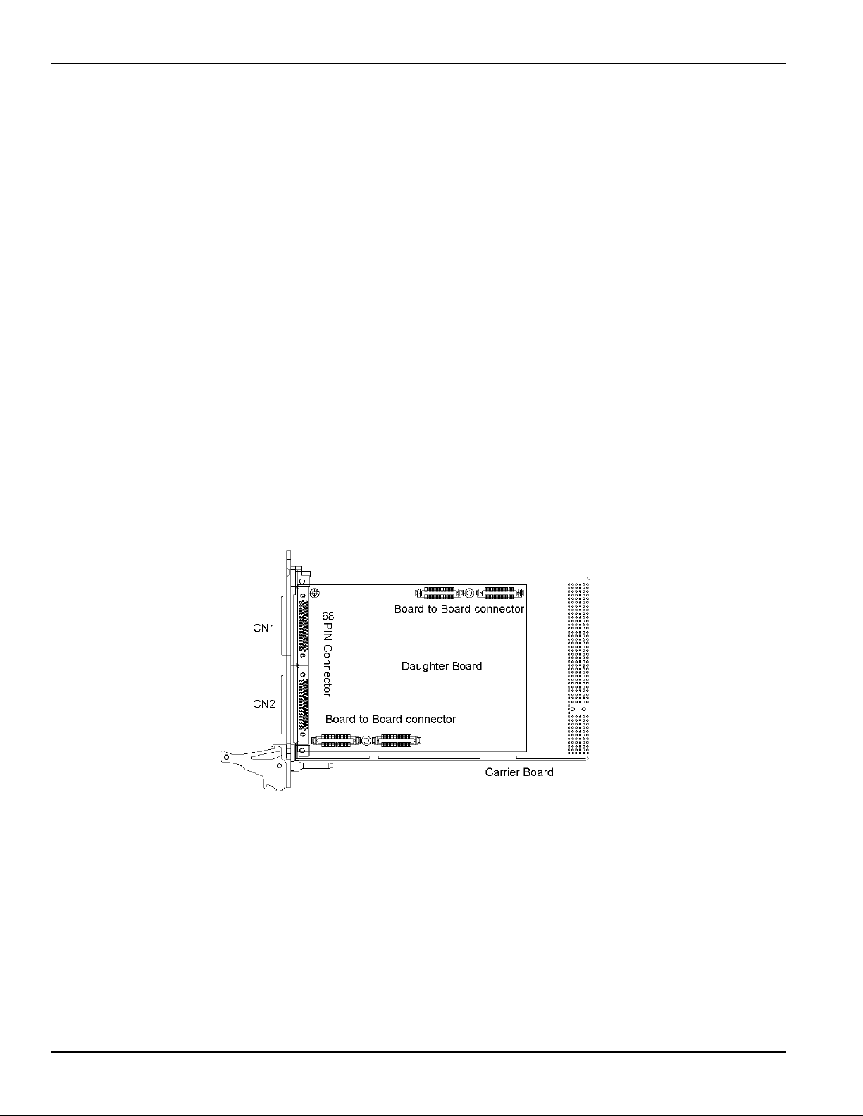
Mechanical Drawing
Figure 2-1
PXI Layout of KPXI-DAQ
®
KPXI series cards. KIDAQ® KPXI series
cards contain electro-static sensitive components that can be easily damaged
by static electricity.
Configuration
Plug and Play
As a plug and play component, the board requests an interrupt number via its PCI controller. The
system BIOS responds with an interrupt assignment based on the board information and system
parameters. These system parameters are determined by the installed drivers and the hardware
load recognized by the system. If this is the first time a KIDAQ
on your Windows
detailed information.
2-2 Return to Section Topics KPXI-DAQ-901-01 Rev. A / January 2007
®
system, a hardware driver needs to be installed. Refer to Installation for
®
KPXI series card will be installed
Page 23

KPXI Multi-Function Module Reference Manual Section 2: Installation
Configuration
Configuration is done on a board-by-board basis for all PXI boards on your system. Configuration
is controlled by the system and software. There is no jumper setting required (or available) for
base address, DMA, and interrupt IRQ.
The configuration is not static, but is subject to change with every boot of the system as new
boards are added or removed.
Troubleshooting
If your system doesn't boot or if you experience erratic operation with your PXI board in place, it's
likely caused by an interrupt conflict (perhaps the BIOS Setup is incorrectly configured). In
general, the solution, is to consult the BIOS documentation that comes with your system.
Installation
Step 1. Install driver software
Windows® will find the new module automatically. If this is the first time a KPXI Series card is
running on your Windows system, you will need to install a hardware driver. Use the following
installation procedure as a guide.
NOTE: Keithley Instruments controllers are pre-loaded with the necessary drivers.
For Windows 2000/XP:
1. Insert the CD shipped with the module. The CD should auto load. From the base menu
install the KDAQ-DRVR. This is the hardware driver that recognizes the KPXI Series
modules. If the CD does not auto load run, then under x:\KDAQ-DRVR\DISK1\, you will find
SETUP.EXE (x is the drive letter of your CDROM). This will also run the install.
2. When you complete driver installation, turn off the system.
Step 2. Inspect module
Keeping the “Handling precautions” information in mind, inspect the module for damage. With the
module placed on a firm, flat surface, press down on all socketed IC's to make sure that they are
properly seated.
If the module does not pass the inspection, do not proceed with the installation.
CAUTION Do not apply power to the card if it has been damaged.
The KPXI Series card is now ready for installation.
Step 3. Install module
Remove power from the system and install the KPXI card in an available slot.
The PXI connectors are rigid and require careful handling when inserted and removed. Improper
handling of modules can easily damage the backplane.
To insert the module into a PXI chassis, use the following procedure as a guide (refer to
Figure 2-2):
1. Turn off the system.
2. Align the module's edge with the card guide in the PXI chassis.
KPXI-DAQ-901-01 Rev. A / January 2007 Return to Section Topics 2-3
Page 24
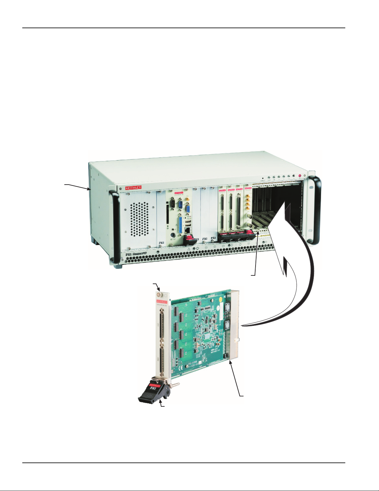
Section 2: Installation KPXI Multi-Function Module Reference Manual
3. Slide the module into the chassis until resistance is felt from the PXI connector.
4. Push the ejector upwards and fully insert the module into the chassis. Once inserted, a
"click" can be heard from the ejector latch.
5. Tighten the screw on the front panel.
6. Turn on the system.
To remove a module from a PXI chassis, use the following procedure as a guide:
1. Turn off the system.
2. Loosen the screw on the front panel.
3. Push the ejector downwards and carefully remove the module from the chassis.
Figure 2-2
Typical PXI module installation
Typical PXI
chassis
Front panel
screw
Card guide
Modules edge
Ejector latch
2-4 Return to Section Topics KPXI-DAQ-901-01 Rev. A / January 2007
Page 25
KPXI Multi-Function Module Reference Manual Section 2: Installation
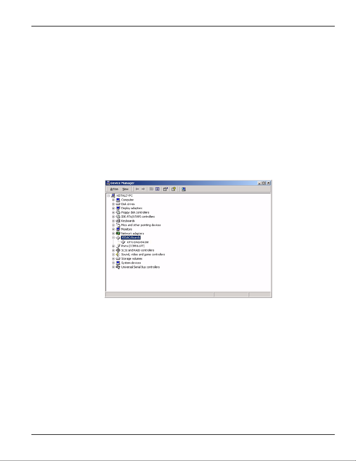
Step 4. Verify installation
When the system is turned on for the first time with a new module present (or a module in a new
slot), Windows Add New Hardware Wizard attempts to locate the correct driver. If it cannot find
the correct driver, even after you have loaded the driver above in Step 1, then force the Add New
Hardware Wizard to look in Windows system32 directory. The driver files should be in this
location. If they are not, shutdown the system, remove the module, and restart the installation
process.
When the Add New Hardware Wizard finishes, the window will verify whether or not installation
was successful. To confirm if the module is installed correctly at a later time, use Windows Device
Manager. In the Device Manager under KIDAQ Boards, look for a device name matching the
model number of the newly installed board (see
installation is complete. If the board appears with a exclamation point or warning in Device
Manager, the installation was unsuccessful. If unsuccessful, use Device Manager to update the
driver or un-install the module, power down the system, remove the module, and attempt
installation again from Step 1.
Figure 2-3
Device manager (successful installation)
Figure 2-3 for an example). If it is found,
KPXI-DAQ-901-01 Rev. A / January 2007 Return to Section Topics 2-5
Page 26

Section 2: Installation KPXI Multi-Function Module Reference Manual
This page left blank intentionally.
2-6 Return to Section Topics KPXI-DAQ-901-01 Rev. A / January 2007
Page 27

In this section:
Top ic Pa ge
Introduction ............................................................................................. 3-2
Signal Connections ................................................................................. 3-2
Operation Theory .................................................................................... 3-9
Section 3
Operation
Connectors Pin Assignment ............................................................. 3-2
Analog Input Signal Connection ....................................................... 3-7
A/D Conversion ................................................................................ 3-9
D/A Conversion .............................................................................. 3-20
Digital I/O........................................................................................ 3-26
General Purpose Timer/Counter Operation.................................... 3-27
Trigger Sources .............................................................................. 3-30
User-controllable Timing Signals.................................................... 3-34
Calibration............................................................................................. 3-38
Loading Calibration Constants........................................................ 3-38
Auto-calibration............................................................................... 3-38
Saving Calibration Constants ......................................................... 3-39
Page 28

Section 3: Operation KPXI Multi-Function Module Reference Manual
Introduction
This section contains operation information on KIDAQ® KPXI series cards including signal
connections. Use this information to aid in the understanding of how to configure and program the
KIDAQ
®
KPXI series modules.
Signal Connections
This section describes the connectors of the KPXI-DAQ module, and the signal connection
between the KPXI-DAQ module and external devices.
Connectors Pin Assignment
Each KPXI-DAQ module is equipped with two 68-pin VHDCI-type connectors (AMP-787254-1).
They are used for digital input / output, analog input / output, and timer/counter signaling, etc. The
pin assignment for the connectors are illustrated in
and also Table 3-1.
Figure 3-1
CN1 pinout (KPXI-DAQ-64-3M/KPXI-DAQ-64-500K/KPXI-DAQ-64-250K)
AI0 (AIH0) 1 35 (AIL0) AI32
AI1 (AIH1) 2 36 (AIL1) AI33
AI2 (AIH2) 3 37 (AIL2) AI34
AI3 (AIH3) 4 38 (AIL3) AI35
AI4 (AIH4) 5 39 (AIL4) AI36
AI5 (AIH5) 6 40 (AIL5) AI37
AI6 (AIH6) 7 41 (AIL6) AI38
AI7 (AIH7) 8 42 (AIL7) AI39
AI8 (AIH8) 9 43 (AIL8) AI40
AI9 (AIH9) 10 44 (AIL9) AI41
AI10 (AIH10) 11 45 (AIL10) AI42
AI11 (AIH11) 12 46 (AIL11) AI43
AI12 (AIH12) 13 47 (AIL12) AI44
AI13 (AIH13) 14 48 (AIL13) AI45
AI14 (AIH14) 15 49 (AIL14) AI46
AI15 (AIH15) 16 50 (AIL15) AI47
AISENSE 17 51 AIGND
AI16 (AIH16) 18 52 (AIL16) AI48
AI17 (AIH17) 19 53 (AIL17) AI49
AI18 (AIH18) 20 54 (AIL18) AI50
AI19 (AIH19) 21 55 (AIL19) AI51
AI20 (AIH20) 22 56 (AIL20) AI52
AI21 (AIH21) 23 57 (AIL21) AI53
AI22 (AIH22) 24 58 (AIL22) AI54
AI23 (AIH23) 25 59 (AIL23) AI55
AI24 (AIH24) 26 60 (AIL24) AI56
AI25 (AIH25) 27 61 (AIL25) AI57
AI26 (AIH26) 28 62 (AIL26) AI58
AI27 (AIH27) 29 63 (AIL27) AI59
AI28 (AIH28) 30 64 (AIL28) AI60
AI29 (AIH29) 31 65 (AIL29) AI61
AI30 (AIH30) 32 66 (AIL30) AI62
AI31 (AIH31) 33 67 (AIL31) AI63
EXTATRIG 34 68 AIGND
* Symbols in “()” are for differential mode connection.
Figure 3-1, Figure 3-2, Figure 3-3, Figure 3-4,
3-2 Return to Section Topics KPXI-DAQ-901-01 Rev. A / January 2007
Page 29

KPXI Multi-Function Module Reference Manual Section 3: Operation
Figure 3-2
CN2 pinout (KPXI-DAQ-64-3M/KPXI-DAQ-64-500K/KPXI-DAQ-64-250K)
DA0OUT 1 35 AOGND
DA1OUT 2 36 AOGND
AOEXTREF 3 37 AOGND
EXTWFTRIG 6 40 DGND
RESERVED 9 43 SDI1 / DGND*
RESERVED 10 44 SDI2 / DGND*
GPTC0_SRC 13 47 DGND
GPTC0_GATE 14 48 DGND
GPTC0_UPDOWN 15 49 DGND
GPTC0_OUT 16 50 DGND
GPTC1_SRC 17 51 DGND
GPTC1_GATE 18 52 DGND
GPTC1_UPDOWN 19 53 DGND
GPTC1_OUT 20 54 DGND
EXTTIMEBASE 21 55 DGND
NC 4 38 NC
DGND 5 39 DGND
EXTDTRIG 7 41 DGND
SSHOUT 8 42 SDI0 / DGND*
AFI1 11 45 SDI3 / DGND*
AFI0 12 46 DGND
PB7 22 56 PB6
PB5 23 57 PB4
PB3 24 58 PB2
PB1 25 59 PB0
PC7 26 60 PC6
PC5 27 61 PC4
DGND 28 62 DGND
PC3 29 63 PC2
PC1 30 64 PC0
PA7 31 65 PA 6
PA5 32 66 PA 4
PA3 33 67 PA 2
PA1 34 68 PA 0
*Pin 42~45 are SDI<0..3> for KPXI-DAQ-64-3M; DGND for KPXI-DAQ-64-500K/
KPXI-DAQ-64-250K
KPXI-DAQ-901-01 Rev. A / January 2007 Return to Section Topics 3-3
Page 30

Section 3: Operation KPXI Multi-Function Module Reference Manual
Figure 3-3
CN1 pinout (KPXI-DAQ-96-3M)
AI0 (AIH0) 1 35 (AIL0) AI48
AI1 (AIH1) 2 36 (AIL1) AI49
AI2 (AIH2) 3 37 (AIL2) AI50
AI3 (AIH3) 4 38 (AIL3) AI51
AI4 (AIH4) 5 39 (AIL4) AI52
AI5 (AIH5) 6 40 (AIL5) AI53
AI6 (AIH6) 7 41 (AIL6) AI54
AI7 (AIH7) 8 42 (AIL7) AI55
AISENSE 9 43 AIGND
AI8 (AIH8) 10 44 (AIL8) AI56
AI9 (AIH9) 11 45 (AIL9) AI57
AI10 (AIH10) 12 46 (AIL10) AI58
AI11 (AIH11) 13 47 (AIL11) AI59
AI12 (AIH12) 14 48 (AIL12) AI60
AI13 (AIH13) 15 49 (AIL13) AI61
AI14 (AIH14) 16 50 (AIL14) AI62
AI15 (AIH15) 17 51 (AIL15) AI63
AI16 (AIH16) 18 52 (AIL16) AI64
AI17 (AIH17) 19 53 (AIL17) AI65
AI18 (AIH18) 20 54 (AIL18) AI66
AI19 (AIH19) 21 55 (AIL19) AI67
AI20 (AIH20) 22 56 (AIL20) AI68
AI21 (AIH21) 23 57 (AIL21) AI69
AI22 (AIH22) 24 58
AI23 (AIH23) 25 59 (AIL23) AI71
AIGND 26 60 AIGND
AI24 (AIH24) 27 61 (AIL24) AI72
AI25 (AIH25) 28 62 (AIL25) AI73
AI26 (AIH26) 29 63 (AIL26) AI74
AI27 (AIH27) 30 64 (AIL27) AI75
AI28 (AIH28) 31 65 (AIL28) AI76
AI29 (AIH29) 32 66 (AIL29) AI77
AI30 (AIH30) 33 67 (AIL30) AI78
AI31 (AIH31) 34 68 (AIL31) AI79
(AIL22) AI70
* Symbols in “()” are for differential mode connection.
3-4 Return to Section Topics KPXI-DAQ-901-01 Rev. A / January 2007
Page 31

KPXI Multi-Function Module Reference Manual Section 3: Operation
Figure 3-4
CN2 pinout (KPXI-DAQ-96-3M)
AI32 (AIH32) 1 35 (AIL32) AI80
AI33 (AIH33) 2 36 (AIL33) AI81
AI34 (AIH34) 3 37 (AIL34) AI82
AI35 (AIH35) 4 38 (AIL35) AI83
AI36 (AIH36) 5 39 (AIL36) AI84
AI37 (AIH37) 6 40 (AIL37) AI85
AI38 (AIH38) 7 41 (AIL38) AI86
AI39 (AIH39) 8 42 (AIL39) AI87
EXTATRIG 9 43 AIGND
AI40 (AIH40) 10 44 (AIL40) AI88
AI41 (AIH41) 11 45 (AIL41) AI89
AI42 (AIH42) 12 46 (AIL42) AI90
AI43 (AIH43) 13 47 (AIL43) AI91
AI44 (AIH44) 14 48 (AIL44) AI92
AI45 (AIH45) 15 49 (AIL45) AI93
AI46 (AIH46) 16 50 (AIL46) AI94
AI47 (AIH47) 17 51 (AIL47) AI95
AIGND 18 52 AIGND
NC 19 53 NC
EXTDTRIG 20 54 AFI0
EXTTIMEBASE 21 55 DGND
PB7 22 56 PB6
PB5 23 57 PB4
PB3 24 58 PB2
PB1 25 59 PB0
PC7 26 60 PC6
PC5 27 61 PC4
DGND 28 62 DGND
PC3 29 63 PC2
PC1 30 64 PC0
PA7 31 65 PA6
PA5 32 66 PA4
PA3 33 67 PA2
PA1 34 68 PA0
Table 3-1
Legend of 68-pin VHDCI-type connectors
Signal Name Reference Direction Description
AIGND -------- -------- Analog ground for AI. All three
ground references (AIGND, AOGND,
and DGND) are connected together
on board
AI<0..63/95> AIGND Input *For KPXI-DAQ-64-3M/KPXI-DAQ-
64-500K/KPXI-DAQ-64-250K
Analog Input Channels 0~63. Each
channel pair, AI<i, i+32> (I=0..31)
can be configured either two singleended inputs or one differential input
pair (marked as AIH<0..31> and
AIL<0..31>)
*For KPXI-DAQ-96-3M only:
Analog Input Channels 0~95. Each
channel pair, AI<i, i+48> (I=0..47)
can be configured either two singleended inputs or one differential input
pair (marked as AIH<0..47> and
AIL<0..47>)
AISENSE AIGND Input Analog Input Sense. This pin is the
reference for any channels
AI<0..63> in NRSE input
configuration
EXTATRIG AIGND Input External AI analog trigger
KPXI-DAQ-901-01 Rev. A / January 2007 Return to Section Topics 3-5
Page 32

Section 3: Operation KPXI Multi-Function Module Reference Manual
Table 3-1 (continued)
Legend of 68-pin VHDCI-type connectors
Signal Name Reference Direction Description
DA0OUT AOGND Output AO channel 0
DA1OUT AOGND Output AO channel 1
AOEXTREF AOGND Input External reference for AO channels
AOGND -------- -------- Analog ground for AO
EXTWFTRIG DGND Input External AO waveform trigger
EXTDTRIG DGND Input External AI digital trigger
RESERVED -------- Output Reserved. Please leave it open
SDI<0..3> (for KPXI-
DAQ-64-3M only)
GPTC<0,1>_SRC DGND Input Source of GPTC<0,1>
GPTC<0,1>_GATE DGND Input Gate of GPTC<0,1>
GPTC<0,1>_OUT DGND Input Output of GPTC<0,1>
GPTC<0,1>_UPDOWN DGND Input Up/Down of GPTC<0,1>
EXTTIMEBASE DGND Input External Timebase
DGND -------- -------- Digital ground
PB<7,0> DGND PIO* Programmable DIO of 8255 Port B
PC<7,0> DGND PIO* Programmable DIO of 8255 Port C
PA< 7,0> DGND PIO* Programmable DIO of 8255 Port A
AFI0 DGND Input Auxiliary Function Input 0
AFI1 DGND Input Auxiliary Function Input 1
DGND Input Synchronous digital inputs. These 4
digital inputs are sampled
simultaneously with the analog
signal input
(ADCONV, AD_START)
(DAWR, DA_START)
Table 3-2
Legend of SSI signals
NOTE The System Synchronization Interface (SSI) signals can be routed to the PXI trigger bus
for multiple module synchronization within a chassis.
SSI timing signal Functionality
SSI_TIMEBASE SSI master: send the TIMEBASE out
SSI slave: accept the SSI_TIMEBASE to replace the internal
TIMEBASE signal.
SSI_ADCONV SSI master: send the ADCONV out
SSI slave: accept the SSI_ADCONV to replace the internal
ADCONV signal.
SSI_SCAN_START SSI master: send the SCAN_START out
SSI slave: accept the SSI_SCAN_START to replace the
internal SCAN_START signal.
SSI_AD_TRIG SSI master: send the internal AD_TRIG out
SSI slave: accept the SSI_AD_TRIG as the digital trigger
signal.
SSI_DAWR SSI master: send the DAWR out.
SSI slave: accept the SSI_DAWR to replace the internal
DAWR signal.
SSI_DA_TRIG SSI master: send the DA_TRIG out.
SSI slave: accept the SSI_DA_TRIG as the digital trigger
signal.
3-6 Return to Section Topics KPXI-DAQ-901-01 Rev. A / January 2007
Page 33

KPXI Multi-Function Module Reference Manual Section 3: Operation
AInA
A
Analog Input Signal Connection
The KPXI-DAQ module provides up to 96 single-ended or 48 differential analog input channels.
You can fill the Channel Gain Queue to get desired combination of the input signal types. The
analog signal can be converted to digital value by the A/D converter. To avoid ground loops and
obtain a more accurate measurement from the A/D conversion, it is quite important to understand
the signal source type and how to choose the analog input modes: RSE, NRSE, and DIFF mode.
Types of signal sources
Floating Signal Sources
A floating signal source means it is not connected in any way to the building’s ground system. A
device with an isolated output is a floating signal source, such as optical isolator outputs,
transformer outputs, and thermocouples.
Ground-Referenced Signal Sources
A ground-referenced signal means it is connected in some way to the building’s system. That is,
the signal source is already connected to a common ground point with respect to the KPXI-DAQ
module, assuming that the computer is plugged into the same power system. Non- isolated
outputs of instruments and devices that plug into the building’s power system are groundreferenced signal sources.
Input Configurations
Single-ended Connections
A single-ended connection is used when the analog input signal is referenced to a ground that can
be shared with other analog input signals. There are 2 different types for single-ended
connections: RSE and NRSE configuration. In RSE configuration, the KPXI-DAQ module board
provides the grounding point for the external analog input signals and is suitable for floating signal
sources. While in NRSE configuration the board doesn’t provide the grounding point, the external
analog input signal provides its own reference grounding point and is suitable for groundreferenced signals.
Referenced Single-ended (RSE) Mode
In referenced single-ended mode, all the input signals are connected to the ground provided by the
KPXI-DAQ module. It is suitable for connections with floating signal sources.
illustration. Note that when more than two floating sources are connected, these sources will be
referenced to the same common ground.
Figure 3-5
Floating source and RSE input connections
Floating
Signal
Source
V1
n = 0, ...,63
V2
CN1
Input Multiplexer
IGND
Instrumentation
-
mplifier
To A / D
Converter
-
Figure 3-5 shows an
KPXI-DAQ-901-01 Rev. A / January 2007 Return to Section Topics 3-7
Page 34

Section 3: Operation KPXI Multi-Function Module Reference Manual
AInA
A
A
A
x
A
A
Non-Referenced Single-ended (NRSE) Mode
To measure ground-referenced signal sources, which are connected to the same ground point,
you can connect the signals in NRSE mode.
Figure 3-6 illustrates the connection. The signals local
ground reference is connected to the negative input of the instrumentation Amplifier (AISENSE pin
on CN1 connector), and the common-mode ground potential between signal ground and the
ground on board will be rejected by the instrumentation amplifier.
Figure 3-6
Ground-referenced sources and NRSE input connections
GroundReferenced
Signal Source
Commonmode noise &
Ground
potential
V1
Vcm
V2
n = 0, ...,63
Input Multiplexer
-
ISENSE
Instrumentation
mplifier
To A/ D
-
Converter
Differential input mode
The differential input mode provides two inputs that respond to signal voltage difference between
them. If the signal source is ground-referenced, the differential mode can be used for the commonmode noise rejection.
Figure 3-7 shows the connection of ground-referenced signal sources under
differential input mode.
Figure 3-7
Ground-referenced source and differential input
Ground
Referenced
Signal
Source
Commonmode noise &
Ground
potential
= 0, ..., 31
Vcm
IxH
IxL
Inpu t Mu ltiplexer
+
-
IGND
Instrumentation
mplifier
To A /D
Converter
-
Figure 3-8 shows how to connect a floating signal source to the KPXI-DAQ module in differential
input mode. For floating signal sources, you need to add a resistor at each channel to provide a
bias return path. The resistor value should be about 100 times the equivalent source impedance. If
the source impedance is less than 100ohms, you can simply connect the negative side of the
signal to AIGND as well as the negative input of the Instrumentation Amplifier without any
resistors. In differential input mode, less noise couples into the signal connections than in singleended mode.
3-8 Return to Section Topics KPXI-DAQ-901-01 Rev. A / January 2007
Page 35

KPXI Multi-Function Module Reference Manual Section 3: Operation
A
A
x
A
A
Figure 3-8
Floating source and differential input
IxH
IxL
Input Multiplexer
+
-
IGND
Instrumentation
mplifier
To A / D
Converter
-
Floating
Signal
Source
= 0, ..., 31
Operation Theory
The operational theory of KPXI-DAQ module functions are described in this section. The functions
include the A/D conversion, D/A conversion, Digital I/O and General Purpose Counter / Timer. The
operation theory can help you understand how to configure and program the KPXI-DAQ module.
A/D Conversion
When using an A/D converter, users should first know about the properties of the signal to be
measured. Users can decide which channel to use and where to connect the signals to the card.
For more information, refer to
and control the A/D signal configurations, including channels, gains, and polarities (Unipolar/
Bipolar).
Analog Input Signal Connection. In addition, users should define
The A/D acquisition is initiated by a trigger source; users must decide how to trigger the A/D
conversion. The data acquisition will start once a trigger condition is matched.
After the end of an A/D conversion, the A/D data is buffered in a Data FIFO. The A/D data can now
be transferred into the PC's memory for further processing.
Two acquisition modes, Software Polling and Scan acquisition are described below. Timing,
trigger modes, trigger sources, and transfer methods are included.
KPXI-DAQ-64-3M/KPXI-DAQ-96-3M AI Data Format
Synchronous Digital Inputs (for KPXI-DAQ-64-3M only)
When each AD conversion is completed, the 12-bit converted digital data accompanied with 4 bits
of SDI<3..0> from CN2 will be latched into the 16-bit register and data FIFO, as shown in
9 and Figure 3-10. Therefore, users can simultaneously sample one analog signal with four digital
signals. The data format of every acquired 16-bit data is of the form:
D11, D10, D9 ....... D1, D0, b3, b2, b1, b0
Where:
D11, D10, D9 ....... D1, D0: 2’s complement A/D 12-bit data
b3, b2, b1, b0: Synchronous Digital Inputs SDI<3..0>
Figure 3-
KPXI-DAQ-901-01 Rev. A / January 2007 Return to Section Topics 3-9
Page 36

Section 3: Operation KPXI Multi-Function Module Reference Manual
A
A
r
A
A
A
A
Figure 3-9
Synchronous Digital Inputs Block Diagram
ADC
nADBUSY
SDI<3..0>
D<11..0>
nADBUSY
16-bit
Register
4
D
12
CLK
16
Data
FIFO
SDI<3..0>
from CN2
From
Instrumentation
mplifie
D_conversion
in
nADCONV
Figure 3-10
Synchronous Digital Inputs timing
D_conversion
nADBUSY
16 bits data(including AD<11..0> and SDI<3..0>
latched into AD Data FIFO
NOTE The analog signal is sampled when an AD conversion starts (falling edge of signal
AD_conversion), while SDI<3..0> are sampled right after an AD conversion is completed
(rising edge of signal nADBUSY). To be precise: SDI<3..0> are sampled with 280ns lag to
the analog signal.
Table 3-3 and Table 3-4 illustrate the ideal transfer characteristics of some input ranges.
Table 3-3
Input ranges and output digital code (KPXI-DAQ-64-3M/KPXI-DAQ-96-3M)
NOTE The last 4 digital codes are SDI<3..0> and is supported in KPXI-DAQ-64-3M only.
Description Bipolar Analog Input Range Digital Code
Full-scale Range ±10V ±5V ±2.5V ±1.25V
Least significant bit 4.88mV 2.44mV 1.22mV 0.61mV
FSR-1LSB 9.9951V 4.9976V 2.4988V 1.2494V 7FFX
Midscale +1LSB 4.88mV 2.44mV 1.22mV 0.61mV 001X
Midscale 0V 0V 0V 0V 000X
Midscale –1LSB -4.88mV -2.44mV -1.22mV -0.61mV FFFX
-FSR -10V -5V -2.5V -1.25V 800X
Table 3-4
Unipolar analog input range (KPXI-DAQ-64-3M/KPXI-DAQ-96-3M)
NOTE The last 4 digital codes are SDI<3..0> and are supported in KPXI-DAQ-64-3M only
Description Unipolar Analog Input Range Digital code
Full-scale Range 0V to 10V 0 to +5V 0 to +2.5V
Least significant bit 2.44mV 1.22mV 0.61mV
FSR-1LSB 9.9976V 4.9988V 2.9994V 7FFX
3-10 Return to Section Topics KPXI-DAQ-901-01 Rev. A / January 2007
Page 37

KPXI Multi-Function Module Reference Manual Section 3: Operation
Table 3-4 (continued)
Unipolar analog input range (KPXI-DAQ-64-3M/KPXI-DAQ-96-3M)
NOTE The last 4 digital codes are SDI<3..0> and are supported in KPXI-DAQ-64-3M only
Midscale +1LSB 5.00244V 2.50122V 1.25061V 001X
Midscale 5V 2.5V 1.25V 000X
Midscale –1LSB 4.9976V 2.4988V 1.2494V FFFX
-FSR 0V 0V 0V 800X
KPXI-DAQ-64-500K/KPXI-DAQ-64-250K AI Data Format
The data format of the acquired 16-bit A/D data is 2’s Complement coding. Table 3-5 and
Table 3-6 shows the valid input ranges and the ideal transfer characteristics.
Table 3-5
Bipolar analog input range (KPXI-DAQ-64-500K/KPXI-DAQ-64-250K)
Description Bipolar Analog Input Range Digital code
Full-scale Range ±10V ±5V ±2.5V ±1.25V
Least significant
bit
FSR-1LSB 9.999695V 4.999847V 2.499924V 1.249962V 7FFF
Midscale +1LSB 305.2uV 152.6uV 76.3uV 38.15uV 0001
Midscale 0V 0V 0V 0V 0000
Midscale -1LSB -305.2uV -152.6uV -76.3uV -38.15uV FFFF
-FSR -10V -5V -2.5V -1.25V 8000
305.2uV 152.6uV 76.3uV 38.15uV
Table 3-6
Unipolar analog input range (KPXI-DAQ-64-500K/KPXI-DAQ-64-250K)
Description Unipolar Analog Input Range Digital code
Full-scale Range 0V to 10V 0 to +5V 0 to +2.5V 0 to +1.25V
Least significant
bit
FSR-1LSB 9.999847V 4.999924V 2.499962V 1.249981V 7FFF
Midscale +1LSB 5.000153V 2.500076V 1.250038V 0.625019V 0001
Midscale 5V 2.5V 1.25V 0.625V 0000
Midscale -1LSB 4.999847V 2.499924V 1.249962V 0.624981V FFFF
-FSR 0V 0V 0V 0V 8000
152.6uV 76.3uV 38.15uV 19.07uV
Software conversion with polling data transfer acquisition mode (Software Polling)
This is the easiest way to acquire a single A/D data. The A/D converter starts one conversion
whenever the dedicated software command is executed. Then the software would poll the
conversion status and read the A/D data back when it is available.
This method is very suitable for applications that needs to process A/D data in real time. Under this
mode, the timing of the A/D conversion is fully controlled under software. However, it is difficult to
control the A/D conversion rate.
Specifying Channels, Gains, and input configurations in the Channel Gain Queue
In Software Polling and Programmable Scan Acquisition mode, the channel, gain, polarity, and
input configuration (RSE, NRSE, or DIFF) can be specified in the Channel Gain Queue. You can
fill the channel number in the Channel Gain Queue in any order. The channel order of acquisition
KPXI-DAQ-901-01 Rev. A / January 2007 Return to Section Topics 3-11
Page 38

Section 3: Operation KPXI Multi-Function Module Reference Manual
will be the same as the order you set in the Channel Gain Queue. Therefore, you can acquire data
with user-defined channel orders and with different settings on each channel.
When the specified channels have been sampled from the first data to the last data in the Channel
Gain Queue, the settings in Channel Gain Queue are maintained. You don’t need to re-configure
the Channel Gain Queue if you want to keep on sampling data in the same order. The maximum
number of entries you can set in the Channel Gain Queue is 512.
Example:
First you can set entries in Channel Gain Queue:
Ch3 with bipolar ±10V, RSE connection
Ch1 with bipolar ±2.5V, DIFF connection
Ch2 with unipolar 5V, NRSE connection
Ch1 with bipolar ±2.5V, DIFF connection
If you read 10 data by software polling method
Then the acquisition sequence of channels is: 3, 1, 2, 1, 3, 1, 2, 1, 3, 1
Programmable scan acquisition mode
Scan Timing and Procedure
It's recommended that this mode be used if your applications need a fixed and precise A/D
sampling rate. You can accurately program the period between conversions of individual channels.
There are at least 4 counters, which need to be specified:
SI_counter (24 bit):Specify the Scan Interval = SI_counter / Timebase
SI2_counter (16 bit):Specify the data Sampling Interval = SI2_counter/Timebase
PSC_counter (24 bit):Specify Post Scan Counts after a trigger event
NumChan_counter (9 bit):Specify the Number of samples per scan
The acquisition timing and the meaning of the 4 counters are illustrated in Figure 3-11.
Timebase Clock Source
In scan acquisition mode, all the A/D conversions start on the output of counters, which use
Timebase as the clock source. By software you can specify the Timebase to be either an internal
clock source (on-board 40MHz) or an external clock input (EXTTIMEBASE) on CN2. The external
clock is useful when you want to acquire data at rates not available with the internal A/D sample
clock. The external clock source should generate TTL-compatible continuous clocks, and the
maximum frequency is 40MHz while the minimum is 1MHz.
3-12 Return to Section Topics KPXI-DAQ-901-01 Rev. A / January 2007
Page 39

KPXI Multi-Function Module Reference Manual Section 3: Operation
A
A
(
)(p
)
Figure 3-11
Scan timing
3 Scans, 4 Samples per scan
(PSC_Counter=3, NumChan_Counter=4)
( channel sequences are specified in Channel Gain Queue)
Ch2
Ch3
Ch1
Ch0
Ch2
Ch3
Ch1
Ch0
Scan_start
D_conversion
Scan_in_progress
SSHOUT
in8 on CN2
cquisition_in_progress
Ch2
Ch3
Ch1
Ch0
Sampling Interval t=
SI2_COUNTER/TimeBase
Scan Interval T=
SI_COUNTER/TimeBase
There are 4 trigger modes to start the scan acquisition, please refer to Trigger Modes for the
details. The data transfer mode will be discussed in Bus-mastering DMA Data Transfer.
NOTE 1. The maximum A/D sampling rate is 3MHz for KPXI-DAQ-64-3M/KPXI-DAQ-96-3M,
500kHz for KPXI-DAQ-64-500K and 250kHz for KPXI-DAQ-64-250K. Therefore, the
minimum setting for SI2_counter is 14 for KPXI-DAQ-64-3M/KPXI-DAQ-96-3M, 80 for
KPXI-DAQ-64-500K and 160 for KPXI-DAQ-64-250K while using the internal Timebase.
2. The SI_counter is a 24-bit counter and the SI2_counter is a 16-bit counter. Therefore,
the maximum scan interval using the internal Timebase = 2
maximum sampling interval between 2 channels using the internal Timebase = 2
24
/40M s = 0.419s, and the
16
/40M
s = 1.638ms.
3. The scan interval can’t be smaller than the product of the data sampling interval and
the NumChan_counter value. The relationship can be represented as:
SI_counter>=SI2_counter * NumChan_counter.
Scan with SSH (KPXI-DAQ-96-3M doesn’t support this function)
You can send the SSHOUT signal on CN2 to an external S&H circuits to sample and hold all
signals if you want to simultaneously sample all channels in a scan, as illustrated in
Figure 3-11.
NOTE The SSHOUT signal is sent to external S&H circuits to hold the analog signal. Users
must implement external S&H circuits on their own to carry out the S&H function. There
are no on-board S&H circuits.
Specifying Channels, Gains, and input configurations in the Channel Gain Queue
Like software polling acquisition mode, the channel, gain, and input configurations can be
specified in the Channel Gain Queue under the scan acquisition mode. Please refer to
Specifying
Channels, Gains, and input configurations in the Channel Gain Queue. Note that in scan
acquisition mode the number of entries in the Channel Gain Queue is normally equivalent to the
value of NumChan_counter (that is, the number of samples per scan).
KPXI-DAQ-901-01 Rev. A / January 2007 Return to Section Topics 3-13
Page 40

Section 3: Operation KPXI Multi-Function Module Reference Manual
Example:
Set:
SI2_counter = 160
SI_counter = 640
PSC_counter = 3
NumChan_counter = 4
Timebase = Internal clock source
Channel entries in the Channel Gain Queue: ch1, ch2, ch0, ch2
Then:
Acquisition sequence of channels: 1, 2, 0, 2, 1, 2, 0, 2, 1, 2, 0, 2
Sampling Interval = 160/40M s = 4 us
Scan Interval = 640/40M s = 16 us
Equivalent sampling rate of ch0, ch1: 62.5kHz
Equivalent sampling rate of ch2: 125kHz
Trigger Modes
KPXI-DAQ module provides 3 trigger sources (internal software, external analog and digital trigger
sources). You must select one of them as the source of the trigger event. A trigger event occurs
when the specified condition is detected on the selected trigger source (For example, a rising edge
on the external digital trigger input).
There are 4 trigger modes (pre-trigger, post-trigger, middle-trigger, and delay-trigger) working with
the 4 trigger sources to initiate different scan data acquisition timing when a trigger event occurs.
They are described as follows. For information of trigger sources, please refer to
Trigger Sources.
Pre-Trigger Acquisition
Use pre-trigger acquisition in applications where you want to collect data before a trigger event.
The A/D starts when you execute the specified function calls to begin the operation, and it stops
when the external trigger event occurs. Users must program the value M in M_counter (16bit) to
specify the amount of stored scanned data before the trigger event. If an external trigger occurs
after M scans of data are converted, the program only stores the last M scans of data, as
illustrated in
Figure 3-12, where M_counter = M =3, NumChan_counter =4, PSC_counter = 0. The
total stored amount of data = NumChan_counter *M_counter =12.
3-14 Return to Section Topics KPXI-DAQ-901-01 Rev. A / January 2007
Page 41

KPXI Multi-Function Module Reference Manual Section 3: Operation
A
A
Aq
A
A
A
Aq
A
Figure 3-12
Pre-trigger (trigger occurs after M scans)
(M_counter = M = 3, NumChan_counter=4, PSC_counter=0)
Trigger
Scan_start
D_conversion
Scan_in_progress
(
SSHOUT
)(pin8 on CN2)
cquisition_in_progress
uired data
Operation start
cquired & stored data
(M scans)
Note that if a trigger event occurs when a scan is in progress, the data acquisition won’t stop until
the scan completes, and the stored M scans of data includes the last scan. Therefore, the first
stored data will always be the first channel entry of a scan (that is, the first channel entry in
the Channel Gain Queue if the number of entries in the Channel Gain Queue is equivalent to the
value of NumChan_counter), no matter when a trigger signal occurs, as illustrated in
Figure 3-13, where M_counter = M =3, NumChan_counter = 4, PSC_counter = 0.
Figure 3-13
Pre-trigger (trigger with scan is in progress)
(M_counter = M = 3, NumChan_counter =4, PSC_counter=0)
Trigger
Scan_start
D_conversion
Scan_in_progress
(SSHOUT)(pin8 on CN2)
cquisition_in_progress
uired data
Operation start
cquired & stored data
(M scans)
Trigger occurs
Data acquisition
won’t stop until a
scan completes
When a trigger signal occurs before the first M scans of data are converted, the amount of stored
data could be fewer than the originally specified amount in NumChan_counter * M_counter, as
illustrated in
Figure 3-14. This situation can be avoided by setting M_enable. If M_enable is set to
1, the trigger signal will be ignored until the first M scans of data are converted, and It assures user
can get M scans of data under pre-trigger mode, as illustrated in
Figure 3-15. However, if
M_enable is set to 0, the trigger signal will be accepted in any time, as illustrated in Figure 3-14.
Note that the total amount of stored data is still always a multiple of NumChan_counter (number of
samples per scan) because the data acquisition won’t stop until a scan is completed.
KPXI-DAQ-901-01 Rev. A / January 2007 Return to Section Topics 3-15
Page 42

Section 3: Operation KPXI Multi-Function Module Reference Manual
A
A
A
A
A
Aq
A
Figure 3-14
Pre-trigger with M_enable = 0 (trigger occurs before M scans)
(M_Counter = M = 3, NumChan_Counter=4, PSC_Counter=0)
Trigger
Scan_start
D_conversion
Scan_in_progress
(SSHOUT)(pin8 on CN2)
cquisition_in_progress
cquired & stored data
(2 scans)
Operation start
Figure 3-15
Pre-trigger with M_enable = 1
(M_counter = M = 3, NumChan_counter=4, PSC_counter=0)
The first M scans
Trigger signals which occur in the shadow
region(the first M scans) will be ignored
Trigger
Scan_start
D_conversion
Scan_in_progress
(SSHOUT)(pin2 on CN2)
cquisition_in_progress
uired data
Operation start
cquired & stored data
(M scans)
NOTE The PSC_counter is set to 0 in pre-trigger acquisition mode.
Middle-Trigger Acquisition
Use middle-trigger acquisition in applications where you want to collect data before and after a
trigger event. The number of scans (M) stored before the trigger is specified by M_counter, while
the number of scans (N) after the trigger is specified by PSC_counter.
Like pre-trigger mode, the number of stored data could be fewer than the specified amount of data
(NumChan_counter *(M+N)) if an external trigger occurs before M scans of data are converted.
The M_enable bit in middle-trigger mode takes the same effect as in pre-trigger mode. If
M_enable is set to 1, the trigger signal will be ignored until the first M scans of data are converted,
and It assures users can get (M+N) scans of data under middle-trigger mode. However, if
M_enable is set to 0, the trigger signal will be accepted at any time.
Figure 3-16 shows the
acquisition timing with M_enable=1.
3-16 Return to Section Topics KPXI-DAQ-901-01 Rev. A / January 2007
Page 43

KPXI Multi-Function Module Reference Manual Section 3: Operation
A
A
Aq
A
A
A
Acq
A
Figure 3-16
Middle trigger with M_enable = 1
(M_Counter=M=3, NumChan_Counter=4, PSC_Counter=N=1)
The first M scans
Trigger signals which occur in the shadow
region (the firs t M sc ans) will be ign ored
Trigger
Scan_start
D_conversion
Scan_in_progress
(SSHOUT)(pin8 on CN2)
cquisition_in_progress
uired data
Operation start
M scans before
trigger
cquired & stored data
(M+N scans)
N scans
after trigger
If a trigger event occurs when a scan is in progress, the stored N scans of data would include this
scan. And the first stored data will always be the first channel entry of a scan, as illustrated in
Figure 3-17.
Figure 3-17
Middle trigger (trigger occurs when a scan is in progress)
(M_Counter=M=2, NumChan_Counter=4, PSC_Counter=N=2)
Trigger occurs when a scan is in progress
Trigger
Scan_start
D_conversion
Scan_in_progress
(SSHOUT)(pin8 on CN2)
cquisition_in_progress
uired data
Operation start
M scans before
trigger
(M+N scans)
N scans
after trigger
cquired & stored data
Post-Trigger Acquisition
Use post-trigger acquisition in applications where you want to collect data after a trigger event.
The number of scans after the trigger is specified in PSC_counter, as illustrated in
Figure 3-18.
The total acquired data length = NumChan_counter *PSC_counter.
KPXI-DAQ-901-01 Rev. A / January 2007 Return to Section Topics 3-17
Page 44

Section 3: Operation KPXI Multi-Function Module Reference Manual
A
A
A
A
A
A
Figure 3-18
Post trigger
(NumChan_Counter=4, PSC_Counter=3)
Trigger
Scan_start
D_conversion
Scan_in_progress
(SSHOUT)(pin8 on CN2
cquisition_in_progress
cquired & stored data
(3 scans)
Operation start
Delay Trigger Acquisition
Use delay trigger acquisition in applications where you want to delay the data collecting process
after the occurrence of a specified trigger event. The delay time is controlled by the value, which is
pre-loaded in the Delay_counter (16bit). The counter counts down on the rising edge of the
Delay_counter clock source after the trigger condition is met. The clock source is software
programmed and can be either the Timebase clock (40MHz) or the A/D sampling clock (Timebase
/SI2_counter). When the count reaches 0, the counter stops and the board starts to acquire data.
The total acquired data length = NumChan_counter * PSC_counter.
Figure 3-19
Delay trigger
(NumChan _Counter=4, PSC_Counter=3)
Trigger
Scan_start
D_conversion
Scan_in_progress
(SSHOUT)(pin8 on CN2)
cquisition_in_progress
Delay until
Delay_Counter
Operation start
reaches 0
NOTE When the Delay_counter clock source is set to Timebase, the maximum delay time = 2
cquired & stored data
(3 scans)
16
40M s = 1.638ms, and when set to A/D sampling clock, the maximum delay time can be
higher (2
16
* SI2_counter / 40M ).
Post-Trigger or Delay-trigger Acquisition with retrigger
Use post-trigger or delay-trigger acquisition with re-trigger function in applications where you want
to collect data after several trigger events. The number of scans after each trigger is specified in
PSC_counter, and users could program Retrig_no to specify the re-trigger numbers.
Figure 3-20
illustrates an example. In this example, 2 scans of data is acquired after the first trigger signal,
then the board waits for the re-trigger signal (re-trigger signals which occur before the first 2 scans
of data acquired will be ignored). When the re-trigger signal occurs, the board scans 2 more scans
/
3-18 Return to Section Topics KPXI-DAQ-901-01 Rev. A / January 2007
Page 45

KPXI Multi-Function Module Reference Manual Section 3: Operation
A
A
A
of data. The process repeats until the specified amount of re-trigger signals are detected. The total
acquired data length = NumChan_counter * PSC_counter * Retrig_no.
Figure 3-20
Post trigger with retrigger
(NumChan _Counter=4, PSC_Counter=2, retrig_no=3)
Trigger
Scan_start
D_conversion
Scan_in_progress
(SSHOUT)(pin8 on CN2)
cquisition_in_progress
cquired & stored data
(6 scan s)
Operation start
Bus-mastering DMA Data Transfer
PCI bus-mastering DMA is necessary for high speed DAQ in order to utilize the maximum PCI
bandwidth. The bus-mastering controller, which is built in the PLX IOP-480 PCI controller, controls
the PCI bus when it becomes the master of the bus. Bus mastering reduces the size of the onboard memory and reduces the CPU loading because data is directly transferred to the computer’s
memory without host CPU intervention.
Bus-mastering DMA provides the fastest data transfer rate on PCI-bus. Once the analog input
operation starts, control returns to your program. The hardware temporarily stores the acquired
data in the on-board AD Data FIFO and then transfers the data to a user-defined DMA buffer
memory in the computer. Please note that even when the acquired data length is less than the
Data FIFO, the AD data will not be kept in the Data FIFO but directly transferred into host memory
by the bus-mastering DMA.
By using a high-level programming library for high speed DMA data acquisition, users simply need
to assign the sampling period and the number of conversion into their specified counters. After the
AD trigger condition is matched, the data will be transferred to the system memory by the busmastering DMA.
The PCI controller also supports the function of scatter/gather bus mastering DMA, which helps
the users to transfer large amounts of data by linking all the memory blocks into a continuous
linked list.
In a multi-user or multi-tasking OS, like Microsoft Windows, it is difficult to allocate a large
continuous memory block to do the DMA transfer. Therefore, the PLX IOP-480 provides the
function of scatter /gather or chaining mode DMA to link the non-continuous memory blocks into a
linked list so that users can transfer very large amounts of data without being limited by the
fragmentation of memory. Users can configure the linked list for the input DMA channel or the
output DMA channel.
Figure 3-21 shows a linked list that is constructed by three DMA descriptors.
Each descriptor contains a PCI address, a local address, a transfer size, and the pointer to the
next descriptor. Users can allocate many small size memory blocks and chain their associative
DMA descriptors altogether by their application programs. KPXI-DAQ module software driver
provides simple settings of the scatter/gather function, and some sample programs are also
provided on the CD.
KPXI-DAQ-901-01 Rev. A / January 2007 Return to Section Topics 3-19
Page 46

Section 3: Operation KPXI Multi-Function Module Reference Manual
Figure 3-21
Scatter/gather DMA for data transfer
In non-chaining mode, the maximum DMA data transfer size is 2M double words (8M bytes).
However, by using chaining mode, scatter/gather, there is no limitation on DMA data transfer size.
Users can also link the descriptor nodes circularly to achieve a multi-buffered mode DMA.
D/A Conversion
NOTE KPXI-DAQ-96-3M does not support this function.
There are 2 channels of 12-bit D/A output available in the KPXI-DAQ module. When using D/A
converters, users should assign and control the D/A converter reference sources for the D/A
operation mode and D/A channels. Users could also select the output polarity: unipolar or bipolar.
The reference selection control lets users fully utilize the multiplying characteristics of the D/A
converters. Internal 10V reference and external reference inputs are available in the KPXI-DAQ
module. The range of the D/A output is directly related to the reference. The digital codes that are
updated to the D/A converters will multiply with the reference to generate the analog output. While
using internal 10V reference, the full range would be –10V ~ +9.9951V in the bipolar output mode,
and 0V ~ 9.9976V in the unipolar output mode. While using an external reference, users can reach
different output ranges by connecting different references. For example, if connecting a DC –5V
with the external reference, then the users can get a full range from –4.9976V to +5V in the bipolar
output with inverting characteristics due to the negative reference voltage. Users could also have
an amplitude modulated (AM) output by feeding a sinusoidal signal into the reference input. The
range of the external reference should be within ±10V.
Table 3-7 and Table 3-8 illustrates the
relationship between digital code and output voltages.
Table 3-7
Bipolar output code table(Vref=10V if internal reference is selected)
Digital Code Analog Output
111111111111 Vref * (2047/2048)
100000000001 Vref * (1/2048)
100000000000 0V
011111111111 -Vref * (1/2048)
000000000000 -Vref
3-20 Return to Section Topics KPXI-DAQ-901-01 Rev. A / January 2007
Page 47

KPXI Multi-Function Module Reference Manual Section 3: Operation
Table 3-8
Unipolar output code table (Vref=10V if internal reference is selected)
Digital Code Analog Output
111111111111 Vref * (4095/4096)
100000000000 Vref * (2048/4096)
000000000001 Vref * (1/4096)
000000000000 0V
The D/A conversion is initiated by a trigger source. Users must decide how to trigger the D/A
conversion. The data output will start when a trigger condition is met. Before the start of D/A
conversion, D/A data is transferred from PC’s main memory to a buffering Data FIFO.
There are two modes of the D/A conversion: Software Update and Timed Waveform Generation
are described, including timing, trigger source control, trigger modes and data transfer methods.
Either mode may be applied to D/A channels independently. You can software update DA CH0
while generate timed waveforms on CH1 at the same time.
Software Update
This is the easiest way to generate D/A output. First, users should specify the D/A output
channels, set output polarity: unipolar or bipolar, and reference source: internal 10V or external
AOEXTREF. Then update the digital values into D/A data registers through a software output
command.
Timed Waveform Generation
This mode can provide your applications with a precise D/A output with a fixed update rate. It can
be used to generate an infinite or finite waveform. You can accurately program the update period
of the D/A converters.
The D/A output timing is provided through a combination of counters in the FPGA on board. There
are in total 5 counters to be specified. These counters are:
UI_counter(24 bits): specify the DA Update Interval = CHUI_counter/Timebase.
UC_counter(24 bits): specify the total Update Counts in a single waveform
IC_counter(24 bits): specify the Iteration Counts of waveform.
DLY1_counter(16 bits): specify the Delay from the trigger to the first update start.
DLY2_counter(16 bits): specify the Delay between two consecutive waveform generations.
Figure 3-22 shows the typical D/A timing diagram. D/A updates its output on each rising edge of
DAWR. The meaning of the counters above is discussed more in the following sections. For more
information of Timebase, please refer to
Timebase Clock Source.
KPXI-DAQ-901-01 Rev. A / January 2007 Return to Section Topics 3-21
Page 48

Section 3: Operation KPXI Multi-Function Module Reference Manual
0
A
Figure 3-22
Typical D/A timing of waveform generation
NOTE Figure 3-22 assumes the data in the buffer is as follows: 2V, 4V, -4V, and 0V.
4 update counts, 3 iterations
Trigger
DAWR
WFG_in_progress
(UC _Counter=4, IC_Counter=3)
UC_Counter=4
Output Waveform
Operation start
Delay until
DLY1_Counter
reaches 0
Delay un til
DLY2_Counter
reaches 0
DA update_interval t=
UI_Counter/Timebase
4
-
single waveform
IC_Counter = 3
Delay un til
DLY2_Counter
reaches 0
NOTE The maximum D/A update rate is 1MHz. Therefore; the minimum setting of UI_counter is
40 while using the internal Timebase (40MHz).
Trigger Modes
Post-Trigger Generation
Use post trigger when you want to perform DA waveform right after a trigger event occurs. In this
trigger mode DLY1_Counter is not used and you don’t need to specify it.
single waveform generated right after a trigger signal is detected. The trigger signal could come
from a software command, an analog trigger or a digital trigger. Please refer to
detailed information.
Figure 3-23 shows a
Trigger Sources for
3-22 Return to Section Topics KPXI-DAQ-901-01 Rev. A / January 2007
Page 49

KPXI Multi-Function Module Reference Manual Section 3: Operation
Figure 3-23
Post trigger waveform generation
NOTE Figure 3-23 assumes the data in the buffer is as follows: 2V, 4V, 6V, 3V, 0V, -4V, -2V, and
4V.
8 update counts, 1 iteration
(UC _Counter=8, IC_Counter=1)
Trigger
DAWR
WFG_in_progress
Output Waveform
-2
-4
Operation start
Delay-Trigger Generation
Use delay trigger when you want to delay the waveform generation after a trigger event. In Figure
3-24, DA_DLY1_counter determines the delay time from the trigger signal to the start of the
waveform generation. DLY1_counter counts down on the rising edge of its clock source after the
trigger condition is met. When the count reaches 0, the counter stops and the KPXI-DAQ module
starts the waveform generation. This DLY1_Counter is 16-bit’s wide and users can set the delay
time in units of TIMEBASE (delay time = DLY1_Counter/TIMEBASE) or in units of update period
(delay time DLY1_Counter * UI_counter/TIMEBASE), such that the delay time can reach a wider
range.
Figure 3-24
Delay trigger waveform generation
NOTE Figure 3-24 assumes the data in data buffer is as follows: 2V, 4V, 6V, 3V, 0V, -4V, -2V,
and 4V.
8 update counts, 1 iteration
Trigger
DAWR
WFG_in_progress
Output W aveform
Operation start
(UC _Counter=8, IC_Counter=1)
Delay un til
DLY1_counter
reaches 0
Post-Trigger or Delay-Trigger with Re-trigger
Use post-trigger or delay-trigger with re-trigger function when you want to generate waveform after
more than one trigger events. The re-trigger function can be enabled or disabled by software
setting. In
Figure 3-25, each trigger signal will generate 2 single waveforms (since IC_Counter =
2), and you can set Retrig_no to specify the number of the accepted re-trigger signals. Note that a
trigger would be ignored if it occurs during waveform generation.
KPXI-DAQ-901-01 Rev. A / January 2007 Return to Section Topics 3-23
Page 50

Section 3: Operation KPXI Multi-Function Module Reference Manual
A
Figure 3-25
Re-triggered waveform generation with Post-trigger and DLY2_Counter = 0
NOTE Figure 3-25 assumes the data in the buffer is as follows: 2V, 4V, 2V, and 0V.
4 update counts, 2 iterations
Trigger
DAWR
WFG_in_progress
Output Waveform
(UC _Counter=4, IC_Counter=2, retrig_no=3)
4
Ignored
Operation start
a single waveform
Iterative Waveform Generation
Set IC_Counter in order to generate iterative waveforms from the data of a single waveform. The
counter stores the iteration number, and the iterations could be finite (
Figure 3-26) or infinite
(Figure 3-27). Note that in infinite mode the waveform generation won’t stop until software stop
function is executed, and IC_Counter is still meaningful when stop mode III is selected.
Please refer to
Stop Modes of Scan Update for details.
A data FIFO on board is used to buffer the digital data for DA output. If the data size of a single
waveform specified (That is, Update Counts in UC_Counter) is less than the FIFO size, after
initially transferring the data from host PC memory to the FIFO on board, the data in FIFO will be
automatically re-transmitted whenever a single waveform is completed. Therefore, it won’t occupy
the PCI bandwidth when the iterative waveforms are performed. However, if the data size of a
single waveform specified is more than the FIFO size, it needs to intermittently perform DMA to
transfer data from host PC memory to the FIFO on board when the iterative waveforms are
performed and occupies PCI bandwidth. The data FIFO size on the KPXI-DAQ module is
1024
(words) when one DA channel is enabled, and 512 (words) when both DA channels are
enabled.
Figure 3-26
Finite iterative waveform generation with Post-trigger and DLY2_Counter = 0
NOTE Figure 3-26 assumes the data in the buffer is as follows: 2V, 4V, 2V, and 0V.
4 update counts, 3 iterations
(UC _Counter=4, IC_Counter=3)
Trigger
DAWR
WFG_in_progress
Output Waveform
single waveform
Operation start
3-24 Return to Section Topics KPXI-DAQ-901-01 Rev. A / January 2007
Page 51

KPXI Multi-Function Module Reference Manual Section 3: Operation
Figure 3-27
Infinite iterative waveform generation with Post-trigger and DLY2_Counter = 0
NOTE Figure 3-27 assumes the data in the buffer is as follows: 2V, 4V, 2V, and 0V.
4 update counts, infinite iterations
(UC _Counter=4, IC_Counter=3)
Trigger
DAWR
WFG_in_progress
Output Waveform
Operation start
waveform generation
won’t stop until software
stop function is
executed
Delay2 in iterative Waveform Generation
To stretch out the flexibility of the D/A waveform generation, we add a DLY2 Counter to separate 2
consecutive waveforms in iterative waveform generation. The time between two waveforms is
assigned by setting the value of DLY2_Counter. The DLY2_Counter counts down after a complete
waveform generation, and when it counts down to zero, the next waveform generation will start.
This DLY2_Counter is 16-bits wide and users can set the delay time in the unit of Timebase (delay
time = DLY2_Counter/Timebase) or in the unit of update period (delay time = DLY2_Counter *
UI_Counter/Timebase), such that the delay time could reach a wide range.
Stop Modes of Scan Update
You can call software stop function to stop waveform generation while it is still in progress. Three
stop modes are provided for timed waveform generation. You can apply these 3 modes to stop
waveform generation regardless of whether infinite or finite waveform generation mode is
selected.
Figure 3-28 illustrates an example for stop mode I, in this mode the waveform stops immediately
when software command is asserted.
In stop mode II, after a software stop command is given, the waveform generation won’t stop until
a complete single waveform is finished. See
Figure 3-29 for an example, since UC_Counter is set
to 4, the total DA updates counts (that is, number of pulses of DAWR signal) must be a multiple of
4 (update counts = 20 in this example).
In stop mode III, after a software stop command is given, the waveform generation won’t stop until
the performed number of waveforms is a multiple of IC_Counter. See
Figure 3-30 for an example,
since IC_Counter is set to 3, the total generated waveforms must be a multiple of 3 (waveforms =
6 in this example), and the total DA update counts must be a multiple of 12 (UC_Counter *
IC_Counter). You can compare these three figures for their differences.
KPXI-DAQ-901-01 Rev. A / January 2007 Return to Section Topics 3-25
Page 52

Section 3: Operation KPXI Multi-Function Module Reference Manual
0
Figure 3-28
Stop mode I
NOTE Figure 3-28 assumes the data in the buffer is as follows: 2V, 4V, 2V, and 0V.
4 update counts, infinite iterations
(UC _Counter=4, IC_Counter=3)
Trigger
DAWR
WFG_in_progress
Output Waveform
Operation start
Software stop command
Figure 3-29
Stop mode II
4 update counts, infinite iterations
(UC _Counter=4, IC_Counter=3)
Trigger
DAWR
Figure 3-30
Stop mode III
Digital I/O
The KPXI-DAQ module contains 24-lines of general-purpose digital I/O (GPIO), which is provided
through a 82C55A chip.
WFG_in_progress
Output Waveform
Operation start
Trigger
DAWR
WFG_in_progress
Output Waveform
Operation start
Software stop command
4 update counts, infinite iterations
(UC _Counter=4, IC_Counter=3)
Software stop command
The 24-lines GPIO are separated into three ports: Port A, Port B and Port C. Port A, Port B, Port C
high nibble (bit-4 to bit-7), and low nibble (bit 0 to bit 3) can be programmed to be input or output
individually. At system startup and reset, all the I/O pins are all reset to be input configuration, that
is, high impedance.
3-26 Return to Section Topics KPXI-DAQ-901-01 Rev. A / January 2007
Page 53

KPXI Multi-Function Module Reference Manual Section 3: Operation
KPXI-DAQ-64-3M also provides 4 digital inputs (SDI from CN2), which are sampled
simultaneously with the analog signal input and stored with the 12-bit AD data. Please refer to
Synchronous Digital Inputs (for KPXI-DAQ-64-3M only) for the details.
General Purpose Timer/Counter Operation
NOTE KPXI-DAQ-96-3M doesn’t support this function.
Two independent 16-bit up/down timer/counter are designed within FPGA for various applications.
They have the following features:
• Count up/down controlled by hardware or software
• Programmable counter clock source (internal or external clock up to 10MHz)
• Programmable gate selection (hardware or software control)
• Programmable input and output signal polarities (high active or low active)
• Initial Count can be loaded from software
• Current count value can be read-back by software without affecting circuit operation
Timer/Counter functions basics
Each timer/counter has three inputs that can be controlled via hardware or software. They are
clock input (GPTC_CLK), gate input (GPTC_GATE), and up/down control input
(GPTC_UPDOWN). The GPTC_CLK input provides a clock source input to the timer/counter.
Active edges on the GPTC_CLK input make the counter increment or decrement. The
GPTC_UPDOWN input controls whether the counter counts up or down. The GPTC_GATE input
is a control signal which acts as a counter enable or a counter trigger signal under different
applications.
The output of timer/counter is GPTC_OUT. After power-up, GPTC_OUT is pulled high by a pulledup resister about 10K ohms. Then GPTC_OUT goes low after the KPXI-DAQ module initialization.
All the polarities of input/output signals can be programmed by software. In this section, for easy
explanation, all GPTC_CLK, GPTC_GATE, and GPTC_OUT are assumed to be active high or
rising-edge triggered in the figures.
General Purpose Timer/Counter modes
Eight programmable timer/counter modes are provided. All modes start operating following a
software-start signal that is set by the software. The GPTC software reset initializes the status of
the counter and re-loads the initial value to the counter. The operation remains halted until the
software-start is re-executed. The operating theories under different modes are described as
below.
Mode1: Simple Gated-Event Counting
In this mode, the counter counts the number of pulses on the GPTC_CLK after the software-start.
Initial count can be loaded from software. Current count value can be read-back by software any
time without affecting the counting. GPTC_GATE is used to enable/disable counting. When
GPTC_GATE is inactive, the counter halts the current count value.
operation with initial count = 5, count-down mode.
Figure 3-31 illustrates the
KPXI-DAQ-901-01 Rev. A / January 2007 Return to Section Topics 3-27
Page 54

Section 3: Operation KPXI Multi-Function Module Reference Manual
Figure 3-31
Mode 1 operation
Software start
Gate
CLK
Count value
55 432110ffff
Mode2: Single Period Measurement
In this mode, the counter counts the period of the signal on GPTC_GATE in terms of GPTC_CLK.
Initial count can be loaded from software. After the software-start, the counter counts the number
of active edges on GPTC_CLK between two active edges of GPTC_GATE. After the completion of
the period interval on GPTC_GATE, GPTC_OUT outputs high and then current count value can be
read-back by software.
Figure 3-32 illustrates the operation where initial count = 0, count-up mode.
Figure 3-32
Mode 2 operation
Software start
Gate
CLK
Count value
00 1234555
Mode 3: Single Pulse-width Measurement
In this mode the counter counts the pulse-width of the signal on GPTC_GATE in terms of
GPTC_CLK. Initial count can be loaded from software. After the software-start, the counter counts
the number of active edges on GPTC_CLK when GPTC_GATE is in its active state. After the
completion of the pulse-width interval on GPTC_GATE, GPTC_OUT outputs high and then current
count value can be read-back by software.
Figure 3-33 illustrates the operation where initial count
= 0, count-up mode.
Figure 3-33
Mode 3 operation
Software start
Gate
CLK
Count value
00 1234555
Mode 4: Single Gated Pulse Generation
This mode generates a single pulse with programmable delay and programmable pulse-width
following the software-start. The two programmable parameters could be specified in terms of
3-28 Return to Section Topics KPXI-DAQ-901-01 Rev. A / January 2007
Page 55

KPXI Multi-Function Module Reference Manual Section 3: Operation
T
periods of the GPTC_CLK input by software. GPTC_GATE is used to enable/disable counting.
When GPTC_GATE is inactive, the counter halts the current count value.
Figure 3-34 illustrates
the generation of a single pulse with a pulse delay of two and a pulse-width of four.
Figure 3-34
Mode 4 operation
Software start
Gate
CLK
Count value
OUT
22 103221 0
Mode5: Single Triggered Pulse Generation
This function generates a single pulse with programmable delay and programmable pulse-width
following an active GPTC_GATE edge. You could specify these programmable parameters in
terms of periods of the GPTC_CLK input. Once the first GPTC_GATE edge triggers the single
pulse, GPTC_GATE takes no effect until the software-start is re-executed.
Figure 3-35 illustrates
the generation of a single pulse with a pulse delay of two and a pulse-width of four.
Figure 3-35
Mode 5 operation
Software start
Gate
CLK
Count value
OUT
22 103210
Figure 38:
Mode6: Re-triggered Single Pulse Generation
This mode is similar to mode5 except that the counter generates a pulse following every active
edge of GPTC_GATE. After the software-start, every active GPTC_GATE edge triggers a single
pulse with programmable delay and pulse-width. Any GPTC_GATE triggers that occur when the
prior pulse is not completed would be ignored.
Figure 3-36 illustrates the generation of two pulses
with a pulse delay of two and a pulse-width of four.
Figure 3-36
Mode 6 operation
S o f t w a r e s t a r t
G a t e
C L K
C o u n t v a l u e
O U
KPXI-DAQ-901-01 Rev. A / January 2007 Return to Section Topics 3-29
22 1032102
I g n o r e d
210
3210 2
2
Page 56

Section 3: Operation KPXI Multi-Function Module Reference Manual
T
T
Mode7: Single Triggered Continuous Pulse Generation
This mode is similar to mode5 except that the counter generates continuous periodic pulses with
programmable pulse interval and pulse-width following the first active edge of GPTC_GATE. Once
the first GPTC_GATE edge triggers the counter, GPTC_GATE takes no effect until the softwarestart is re-executed.
Figure 3-37 illustrates the generation of two pulses with a pulse delay of four
and a pulse-width of three.
Figure 3-37
Mode 7 operation
S o f t w a r e s t a r t
G a t e
C L K
C o u n t v a l u e
O U
4 4 4 3 2 1 0 2 1
0321021
032
Mode8: Continuous Gated Pulse Generation
This mode generates periodic pulses with programmable pulse interval and pulse-width following
the software-start. GPTC_GATE is used to enable/disable counting. When GPTC_GATE is
inactive, the counter halts the current count value.
Figure 3-38 illustrates the generation of two
pulses with a pulse delay of four and a pulse-width of three.
Figure 3-38
Mode 8 operation
S o f t w a r e s t a r t
G a t e
C L K
C o u n t v a l u e
O U
Trigger Sources
The KPXI-DAQ series provides flexible trigger selections. In addition to the internal software
trigger, KPXI-DAQ module also supports external analog, digital triggers and SSI triggers. Users
can configure the trigger source by software for A/D and D/A processes individually. Note that the
A/D and the D/A conversion share the same analog trigger.
Software-Trigger
This trigger mode does not need any external trigger source. The trigger asserts right after you
execute the specified function calls to begin the operation. A/D and D/A processes can receive an
individual software trigger.
External Analog Trigger
4 4 3 3 2 1 0 2 1
0321021
103
The analog trigger circuitry routing is shown in the Figure 3-39. The analog multiplexer could
select either a direct analog input from the EXTATRIG pin (SRC1 in Figure 3-39) on the 68-pin
connector CN1 or the input signal of ADC (SRC2 in Figure 3-39. That is, the first channel input you
fill in the Channel Gain Queue). SRC1 can be used for all trigger modes while SRC2 can only be
used for post and delay trigger modes. The range of trigger level for SRC1 is ±10V and the
resolution is 78mV (please refer to
Table 3-9, the valid code range is from 1 to 255), while the
trigger range of SRC2 is the full-scale range of the first channel input in Channel Gain Queue, and
3-30 Return to Section Topics KPXI-DAQ-901-01 Rev. A / January 2007
Page 57

KPXI Multi-Function Module Reference Manual Section 3: Operation
A
A
A
the resolution is the desired range divided by 256. For example, if the first channel input in
Channel Gain Queue is CH0 with bipolar ±5V range, the trigger voltage would be 4.96V when the
trigger level code is set to 0xFF while –4.96V when the code is set to 0x01.
Figure 3-39
Analog trigger block diagram
Input Multipexer
CN1
In
Instrumentation
mplifier
/D
Converter
n = 0, ...,63
EXTATRIG
SRC2
MUX
SRC1
Analog
Trigger
Circuit
Table 3-9
Analog trigger SRC1 (EXTATRIG) ideal transfer characteristic
Trigger Level digital setting Trigger voltage
0xFF 9.92V
0xFE 9.84V
--- --0x81 0.08V
0x80 0
0x7F -0.08V
--- --0x01 -9.92V
The trigger signal is generated when the analog trigger condition is satisfied. There are five analog
trigger conditions in KPXI-DAQ modules. KPXI-DAQ modules use two threshold voltages:
Low_Threshold and High_ Threshold to build the five different trigger conditions. Users could
configure the trigger conditions easily by software.
Below-Low analog trigger condition
Figure 3-40 shows the below-low analog trigger condition, the trigger signal is generated when the
input analog signal is less than the Low_Threshold voltage, and the High_Threshold setting is not
used in this trigger condition.
Figure 3-40
Below-Low analog trigger condition
KPXI-DAQ-901-01 Rev. A / January 2007 Return to Section Topics 3-31
Page 58

Section 3: Operation KPXI Multi-Function Module Reference Manual
Above-High analog trigger condition
Figure 3-41 shows the above-high analog trigger condition, the trigger signal is generated when
the input analog signal is higher than the High_Threshold voltage, and the Low_Threshold setting
is not used in this trigger condition.
Figure 3-41
Above-High analog trigger condition
Inside-Region analog trigger condition
Figure 3-42 shows the inside-region analog trigger condition, the trigger signal is generated when
the input analog signal level falls in the range between the High_Threshold and the
Low_Threshold voltages. The High_Threshold setting should be always higher than the
Low_Threshold voltage setting.
Figure 3-42
Inside-Region analog trigger condition
High-Hysteresis analog trigger condition
Figure 3-43 shows the high-hysteresis analog trigger condition, the trigger signal is generated
when the input analog signal level is greater than the High_Threshold voltage, and the
Low_Threshold voltage determines the hysteresis duration.
NOTE The High_Threshold setting should be always higher than the Low_Threshold voltage
setting.
3-32 Return to Section Topics KPXI-DAQ-901-01 Rev. A / January 2007
Page 59

KPXI Multi-Function Module Reference Manual Section 3: Operation
Figure 3-43
High-Hysteresis analog trigger condition
Low-Hysteresis analog trigger condition
Figure 3-44 shows the low-hysteresis analog trigger condition, the trigger signal is generated when
the input analog signal level is less than the Low_Threshold voltage, and the High_Threshold
voltage determines the hysteresis duration.
NOTE The High_Threshold setting should be always higher than the Low_Threshold voltage
setting.
Figure 3-44
Low-Hysteresis analog trigger condition
External Digital Trigger
An external digital trigger occurs when a rising edge or a falling edge is detected on the digital
signal connected to the EXTDTRIG or the EXTWFTRG of the 68-pin connector for external digital
trigger. The EXTDTRIG is dedicated for A/D process, and the EXTWFTRG is used for D/A
process. Users can program the trigger polarity through Keithley Instruments’ software drivers
easily. Note that the signal level of the external digital trigger signals should be TTL-compatible,
and the minimum pulse is 20ns.
KPXI-DAQ-901-01 Rev. A / January 2007 Return to Section Topics 3-33
Page 60

Section 3: Operation KPXI Multi-Function Module Reference Manual
Figure 3-45
External digital trigger
User-controllable Timing Signals
In order to meet the requirements for user-specific timing and the requirements for synchronizing
multiple cards, the KPXI-DAQ series provides flexible user-controllable timing signals to connect
to external circuitry or additional cards.
The whole DAQ timing of the KPXI-DAQ series is composed of a bunch of counters and trigger
signals in the FPGA. These timing signals are related to the A/D, D/A conversions and Timer/
Counter applications. These timing signals can be inputs to or outputs from the I/O connectors or
the PXI bus. Therefore the internal timing signals can be used to control external devices or
circuitry’s operation.
We implemented signal multiplexers in the FPGA to individually choose the desired timing signals
for the DAQ operations, as shown in the
Figure 3-46.
Figure 3-46
DAQ signals routing
Internal timing
signals
SSI timing
Signals
AFI timing
signals
DAQ timing
signals
SSI timing
Signals
Trigger_Out
timing signals
Users can utilize the flexible timing signals through our software drivers, and simply and correctly
connect the signals with the KPXI-DAQ series cards. Here is the summary of the DAQ timing
signals and the corresponding functionality for KPXI-DAQ series.
Table 3-10
Summary of user-controllable timing signals
Timing signal
category
SSI/PXI signals Multiple cards synchronization
AFI signals Control KPXI-DAQ module by external timing signals
Corresponding functionality
DAQ timing signals
NOTE SCAN_START, ADCONV and DA_TRIG, DAWR are supported by KPXI-DAQ-96-3M.
3-34 Return to Section Topics KPXI-DAQ-901-01 Rev. A / January 2007
Page 61

KPXI Multi-Function Module Reference Manual Section 3: Operation
The user-controllable DAQ timing-signals include:
NOTE Refer to Scan Timing and Procedure for the internal timing signal definition.
• TIMEBASE, providing TIMEBASE for all DAQ operations, which could be from internal
40MHz oscillator, EXTTIMEBASE from I/O connector or the SSI_TIMEBASE. Note that the
frequency range of the EXTTIMEBASE is 1MHz to 40MHz, and the EXTTIMEBASE should
be TTL-compatible.
• AD_TRIG, the trigger signal for the A/D operation, which could come from external digital
trigger, analog trigger, internal software trigger and SSI_AD_TRIG. Refer to
Trigger Sources
for detailed description.
• SCAN_START, the signal to start a scan, which would bring the following ADCONV signals
for AD conversion, and could come from the internal SI_counter, AFI[0] and
SSI_AD_START. This signal is synchronous to the TIMEBASE. Note that the AFI[0] should
be TTL-compatible and the minimum pulse width should be the pulse width of the
TIMEBASE to guarantee correct functionality.
• ADCONV, the conversion signal to initiate a single conversion, which could be derived from
internal counter, AFI[0] or SSI_ADCONV. Note that this signal is edge-sensitive. When
using AFI[0] as the external ADCONV source, each rising edge of AFI[0] would bring an
effective conversion signal. Also note that the AFI[0] signal should be TTL-compatible and
the minimum pulse width is 20ns.
• DA_TRIG, the trigger signal for the D/A operation, which could be derived from external
digital trigger, analog trigger, internal software trigger and SSI_AD_TRIG. Refer to
Trigger
Sources for detailed description.
• DAWR, the update signal to initiate a single D/A conversion, which could be derived from
internal counter, AFI[1] or SSI_DAWR. Note that this signal is edge-sensitive. When using
AFI[1] as the external DAWR source, each rising edge of AFI[1] would bring an effective
update signal. Also note that the AFI[1] signal should be TTL-compatible and the minimum
pulse width is 20ns.
NOTE The System Synchronization Interface (SSI) signals can be routed to the PXI trigger bus
for multiple module synchronization within a chassis.
Auxiliary Function Inputs (AFI)
NOTE EXTWFTRIG and AFI[1] are NOT supported by KPXI-DAQ-96-3M.
Users could use the AFI in applications that take advantage of external circuitry to directly control
the KPXI-DAQ cards. The AFI includes 2 categories of timing signals: one group is the dedicated
input, and the other is the multi-function input.
Table 3-11 illustrates this categorization.
KPXI-DAQ-901-01 Rev. A / January 2007 Return to Section Topics 3-35
Page 62

Section 3: Operation KPXI Multi-Function Module Reference Manual
A summary of the auxiliary function input signals and the corresponding functionality is contained
in
Table 3-11.
Table 3-11
Auxiliary function input signals
Category Timing signal Functionality Constraints
Dedicated input EXTTIMEBASE Replace the internal
TIMEBASE
EXTDTRIG External digital trigger input
for A/D operation
EXTWFTRG External digital trigger input
for D/A operation
Multi-function input AFI[0]
(Dual functions)
AFI[1] Replace the internal DAWR TTL-compatible
Replace the internal
ADCONV
Replace the internal
SCAN_START
TTL-compatible
1MHz to 40MHz
Affects on both A/D and D/A
operations
TTL-compatible
Minimum pulse width = 20ns
Rising edge or falling edge
TTL-compatible
Minimum pulse width = 20ns
Rising edge or falling edge
TTL-compatible
Minimum pulse width = 20ns
Rising–edge sensitive only
TTL-compatible
Minimum Pulse width > 2/
TIMEBASE
Minimum pulse width = 20ns
Rising–edge sensitive only
EXTDTRIG and EXTWFTRIG
EXTDTRIG and EXTWFTRIG are dedicated digital trigger input signals for A/D and D/A operations
respectively. Please refer to
External Digital Trigger for detailed descriptions.
EXTTIMEBASE
When the applications needs specific sampling frequency or update rate that the card could not
generate from its internal TIMEBASE, the 40MHz clock, users could utilize the EXTTIMEBASE
with internal counters to achieve the specific timing intervals for both A/D and D/A operations. Note
that once you choose the TIMEBASE source, both A/D and D/A operations will be affected
because A/D and D/A operations share the same TIMEBASE
AFI[0]
Alternatively, users can also directly apply an external A/D conversion signal to replace the internal
ADCONV signal. This is another way to achieve customized sampling frequencies. The external
ADCONV signal can only be inputted from the AFI[0]. As
A/D Conversion describes, the
SI_counter triggers the generation of the A/D conversion signal, ADCONV, but when using the
AFI[0] to replace the internal ADCONV signal, then the SI_counter and the internally generated
SCAN_START will not be effective. By controlling the ADCONV externally, users can sample the
data according to external events. In this mode, the Trigger signal and trigger mode settings are
not available.
AFI[0] could also be used as SCAN_START signal for A/D operations. Please refer to A/D
Conversion and DAQ timing signals for detailed descriptions of the SCAN_START signal. When
using external signal (AFI[0]) to replace the internal SCAN_START signal, the pulse width of the
AFI[0] must be greater than two times the period of Timebase. This feature is suitable for the KPXI
series which can scan multiple channels of data controlled by an external event. Note that the
AFI[0] is a multi-purpose input, and it can only be utilized for one function at any one time.
3-36 Return to Section Topics KPXI-DAQ-901-01 Rev. A / January 2007
Page 63

KPXI Multi-Function Module Reference Manual Section 3: Operation
AFI[1]
Regarding the D/A operations, users could directly input the external D/A update signal to replace
the internal DAWR signal. This is another way to achieve customized D/A update rates. The
external DAWR signal can only be inputted from the AFI[1]. Note that the AFI[1] is a multi-purpose
input, and it can only be utilized for one function at any one time. AFI[1] currently only has one
function. Keithley Instruments reserves it for future development.
System Synchronization Interface
SSI (System Synchronization Interface) provides the DAQ timing synchronization between
multiple cards. In KPXI-DAQ series, we designed a bi-directional SSI I/O to provide flexible
connection between cards and allow one SSI master to output the signal and up to three slaves to
receive the SSI signal. Note that the SSI signals are designed for card synchronization only, not for
external devices.
Table 3-12
SSI timing signal summary
SSI timing signal Functionality
SSI_TIMEBASE SSI master: send the TIMEBASE out
SSI slave: accept the SSI_TIMEBASE to replace the internal
TIMEBASE signal.
Note: Affects on both A/D and D/A operations
SSI_AD_TRIG SSI master: send the internal AD_TRIG out
SSI slave: accept the SSI_AD_TRIG as the digital trigger signal.
SSI_ADCONV SSI master: send the ADCONV out
SSI slave: accept the SSI_ADCONV to replace the internal ADCONV
signal.
SSI_SCAN_STARTSSI master: send the SCAN_START out
SSI slave: accept the SSI_SCAN_START to replace the internal
SCAN_START signal.
SSI_DA_TRIG SSI master: send the DA_TRIG out.
SSI slave: accept the SSI_DA_TRIG as the digital trigger signal.
SSI_DAWR SSI master: send the DAWR out.
SSI slave: accept the SSI_DAWR to replace the internal DAWR signal.
In PXI form factor, we utilize the PXI trigger bus built on the PXI backplane to provide the
necessary timing signal connections. All the SSI signals are routed to the P2 connector. No
additional cable is needed. For detailed information of the PXI specifications, please refer to PXI
specification Revision 2.0 from PXI System Alliance (www.pxisa.org).
The 6 internal timing signals could be routed to the PXI trigger bus through software drivers.
Please refer to
DAQ timing signals for detailed information of the 6 internal timing signals.
Physically the signal routings are accomplished in the FPGA. Cards that are connected together
through the SSI or the PXI trigger bus, will still achieve synchronization on the 6 timing signals.
The mechanism of the SSI/PXI
1. We adopt master-slave configuration for SSI/PXI. In a system, for each timing signal, there
shall be only one master, and other cards are SSI slaves or with the SSI function disabled.
2. For each timing signal, the SSI master doesn’t have to be in a single card.
For example:
We want to synchronize the A/D operation through the ADCONV signal for 4 KPXI-DAQ
cards. Card 1 is the master, and Card 2, 3, 4 are slaves. Card 1 receives an external
digital trigger to start the post trigger mode acquisition. The SSI setting could be:
KPXI-DAQ-901-01 Rev. A / January 2007 Return to Section Topics 3-37
Page 64

Section 3: Operation KPXI Multi-Function Module Reference Manual
• Set the SSI_ADCONV signal of Card 1 to be the master.
• Set the SSI_ADCONV signals of Card 2, 3, 4 to be the slaves.
• Set external digital trigger for Card 1’s A/D operation.
• Set SI_counter, SI2_counter, NumChan_counter and the post scan counter (PSC)
on all other cards.
• Start DMA operations for all cards, thus all the cards are waiting for the trigger
event.
When the digital trigger condition of Card 1 occurs, Card 1 will internally generate the
ADCONV signal and output this ADCONV signal to SSI_ADCONV signal of Card 2, 3
and 4 through the SSI/PXI connectors. Thus we can achieve simultaneous acquisition
across four modules.
You could arbitrarily choose each of the 6 timing signals as the SSI master from any one
of the cards. The SSI master can output the internal timing signals to the SSI slaves.
With the SSI, users could achieve better card-to-card synchronization.
Note that when power-up or reset, the DAQ timing signals are reset to use the internal
generated timing signals.
Calibration
This section introduces the calibration process to minimize AD measurement errors and DA output
errors.
Loading Calibration Constants
The KPXI-DAQ modules are factory calibrated before shipment by writing the associated
calibration constants of TrimDACs to the on-board EEPROM. TrimDACs are devices containing
multiple DACs within a single package. TrimDACs do not have memory capability. That means the
calibration constants do not retain their values after the system power is turned off. Loading
calibration constants is the process of loading the values of TrimDACs stored in the on-board
EEPROM. Keithley Instruments provides software to make it easy to read the calibration constants
automatically when necessary.
There is a dedicated space for calibration constants in the EEPROM. In addition to the default
bank of factory calibration constants, there are three extra user-modifiable banks. This means
users can load the TrimDACs values either from the original factory calibration or from a
calibration that is subsequently performed.
Because of the fact that errors in measurements and outputs will vary with time and temperature, it
is recommended to conduct re-calibration when the card is installed in the users environment. The
auto-calibration function used to minimize errors will be introduced in the next sub-section.
Auto-calibration
By using the auto-calibration feature of the KPXI-DAQ module, the calibration software can
measure and correct almost all the calibration errors without any external signal connections,
reference voltages, or measurement devices.
The KPXI-DAQ module has an on-board calibration reference to ensure the accuracy of autocalibration. The reference voltage is measured at the factory and adjusted through a digital
potentiometer by using an ultra-precision calibrator. The impedance of the digital potentiometer is
memorized after this adjustment. It is not recommended for users to adjust the on-board
calibration reference except when an ultra-precision calibrator is available.
3-38 Return to Section Topics KPXI-DAQ-901-01 Rev. A / January 2007
Page 65

KPXI Multi-Function Module Reference Manual Section 3: Operation
NOTE 1. Before auto-calibration procedure starts, it is recommended to warn up the card for at
least 15 minutes.
2. Please remove the cable before an auto-calibration procedure is initiated because the
DA outputs would be changed in the process of calibration.
Saving Calibration Constants
After an auto-calibration is completed, users can save the new calibration constants into one of the
three user-modifiable banks in the EEPROM. The date and the temperature when you ran the
auto-calibration will be saved accompanied with the calibration constants. This means users can
store three sets of calibration constants according to three different environments and re-load the
calibration constants later.
KPXI-DAQ-901-01 Rev. A / January 2007 Return to Section Topics 3-39
Page 66

Section 3: Operation KPXI Multi-Function Module Reference Manual
This page left blank intentionally.
3-40 Return to Section Topics KPXI-DAQ-901-01 Rev. A / January 2007
Page 67

In this appendix:
Top ic Page
Introduction to KDAQ-DRVR................................................................... A-2
About the KDAQ-DRVR software .....................................................A-2
KDAQ-DRVR hardware support .......................................................A-2
KDAQ-DRVR language support .......................................................A-2
Fundamentals of building applications with KDAQ-DRVR ...................... A-3
Microsoft® Visual Basic (Version 6.0)............................................... A-3
Using Microsoft Visual Basic.NET ....................................................A-4
Microsoft Visual C/C++.....................................................................A-4
KDAQ-DRVR utilities for Win32 ..............................................................A-5
KDAQ-DRVR configuration utility (configdrv) ................................... A-5
KDAQ-DRVR data file converter utility (KiDAQCvt).......................... A-6
Appendix A
KDAQ-DRVR User’s Guide
KDAQ-DRVR overview ...........................................................................A-6
General configuration function group ...............................................A-7
Analog input function group.............................................................. A-7
Analog output function group..........................................................A-10
Digital input function group .............................................................A-12
Digital output function group........................................................... A-13
General timer/counter function group ............................................. A-13
DIO function group ......................................................................... A-13
SSI function group .......................................................................... A-14
Calibration function group...............................................................A-14
KDAQ-DRVR application hints.............................................................. A-15
Analog input programming hints .....................................................A-16
Analog output programming hints ......................................................... A-36
One-shot analog output programming scheme ..............................A-36
Digital input programming hints ......................................................A-50
Digital output programming hints.................................................... A-51
DAQ event message programming hints........................................ A-52
Continuous data transfer in KDAQ-DRVR ............................................ A-53
Continuous data transfer mechanism.............................................A-53
Double-buffered AI/AO operation ................................................... A-53
Single-buffered versus double-buffered data transfer .................... A-54
Pre-trigger mode/middle-trigger data acquisition (AI) ..................... A-54
Page 68

Appendix A: KDAQ-DRVR User’s Guide KPXI Multi-Function Module Reference Manual
Introduction to KDAQ-DRVR
About the KDAQ-DRVR software
KDAQ-DRVR is a software development kit for Keithley Instruments KPXI-DAQ cards. It contains
a high performance data acquisition driver for developing custom applications under Microsoft
Windows
KDAQ-DRVR was developed to provide a simple programming interface in communication with
the Keithley Instruments' KPXI-DAQ Series cards. The KDAQ-DRVR’s easy-to-use memory and
data-buffer management capabilities frees developers from these issues but still allows high-level
access to the card’s features.
Using KDAQ-DRVR also takes advantage of the power and features of Win32® System for data
acquisition applications, including the ability to run multiple applications and utilize extended
memory. Using KDAQ-DRVR in a Visual Basic
interfaces and graphics.
In addition to the software drivers, sample programs are provided for your reference. These
sample programs will save programming time and highlight some of the KPXI-DAQ Series cards
features.
®
XP/2000 environments.
®
environment makes it easy to create custom user
KDAQ-DRVR hardware support
Keithley Instruments will periodically upgrade the KDAQ-DRVR for new KPXI- DAQ cards. Refer
to the Release Notes for the most recent list of cards that the current KDAQ-DRVR supports. The
following cards are supported by KDAQ-DRVR:
• KPXI-SDAQ-4-2M: 2MHz 4 channels simultaneous A/D and 2 channels D/A output device
with bus mastering DMA transfer capability
• KPXI-SDAQ-4-500K: 500kHz 4 channels simultaneous A/D and 2 channels D/A output
device with bus mastering DMA transfer capability
• KPXI-DAQ-64-3M: 3MHz 64 channels multiplexed A/D and 2 channels D/A output device
with bus mastering DMA transfer capability
• KPXI-DAQ-64-500K: 500kHz 64 channels multiplexed A/D and 2 channels D/A output
device with bus mastering DMA transfer capability
• KPXI-DAQ-64-250K: 250kHz 64 channels multiplexed A/D and 2 channels D/A output
device with bus mastering DMA transfer capability
• KPXI-DAQ-96-3M: 3MHz 96 channels multiplexed A/D device with bus mastering DMA
transfer capability
• KPXI-AO-4-1M: High performance, 4 channels analog output, multi-function device with
bus mastering DMA transfer capability
• KPXI-AO-8-1M: High performance, 8 channels analog output, multi-function device with
bus mastering DMA transfer capability
KDAQ-DRVR language support
KDAQ-DRVR is the DLL (Dynamic-Link Library) version for use with Windows XP/2000. It works
with any Windows programming language that allows calls to a DLL, such as Microsoft Visual C/
C++ (4.0 or above), Borland C++ (5.0 or above), or Microsoft Visual Basic (4.0 or above).
A-2 Return to Section Topics KPXI-DAQ-901-01 Rev. A / January 2007
Page 69

KPXI Multi-Function Module Reference Manual Appendix A: KDAQ-DRVR User’s Guide
Fundamentals of building applications with KDAQ-DRVR
The following paragraphs outline how to create Windows KDAQ-DRVR projects using Microsoft®
Visual Basic
®
(Version 6.0), Microsoft Visual Basic.NET, and Microsoft Visual C/C++.
Microsoft® Visual Basic (Version 6.0)
To create a Windows® XP/2000 Keithley KDAQ-DRVR application using the API and Microsoft
Visual Basic, follow these steps:
Step 1: Enter Visual Basic and open or create a project to use KDAQ-DRVR
To create a new project, select New Project from the File menu.
To use an existing project:
1. Open the file by selecting Open Project from the File menu. The Open Project dialog box
appears (Figure A-1).
Figure A-1
Open Project dialog box
2. Load the project by finding and double-clicking the project file name in the applicable
directory.
Step 2: Include function declarations and constants file (KDAQDRVR.BAS)
If it is not already included in the project, add the KDAQDRVR.BAS file as a module to your
project. All function declarations and constants are contained in this file. These function
declarations and constants are used to develop user data acquisition applications.
Step 3: Design the application interface
Add elements, such as a command button, list box, or text box, etc., on the Visual Basic form used
to design the interface. These elements are standard controls from the Visual Basic Toolbox. To
place a needed control on the form:
1. Select the needed control from the Toolbox.
2. Draw the control on the form. Alternatively, to place the default-sized control on the form,
click the form. Use the Select Objects tool to reposition or resize controls.
KPXI-DAQ-901-01 Rev. A / January 2007 Return to Section Topics A-3
Page 70

Appendix A: KDAQ-DRVR User’s Guide KPXI Multi-Function Module Reference Manual
Step 4: Set control properties
Set control properties from the properties list. To view the properties list, select the desired control
and do one of the following:
• Press F4
• Select the Properties command in the View menu
or
• Click the Properties button on the Toolbar.
Step 5: Write the event codes
The event codes define the action desired when an event occurs. To write the event codes:
1. Double-click the control or form needing event code (the code module will appear).
2. Add new code as needed. All functions that are declared in KDAQDRVR.BAS can be called
to perform data acquisition operations (refer to tables contained later in this manual).
Step 6: Run your application
To run the application, either:
• Press F5
•Select Start from the Run menu
or
• Click the Start icon on the Toolbar
Using Microsoft Visual Basic.NET
To create a data acquisition application using KDAQ-DRVR and Visual Basic.NET, use the
procedure for
KDAQDRVR.VB (instead of the file named KDAQDRVR.BAS).
Microsoft® Visual Basic (Version 6.0) as an outline, but in step 2, use the file named
Microsoft Visual C/C++
To create a Windows XP/2000 KDAQ-DRVR library application using the KDAQ-DRVR function
library and Microsoft Visual C/C++, follow these steps:
Step 1: Enter Visual C/C++ and open or create a project that will use the
KDAQ-DRVR
NOTE The project can be a new or existing one.
Step 2: Include function declarations and constants file (KDAQDRVR.H)
Include KDAQDRVR.H in the C/C++ source files that call KDAQ-DRVR functions by adding the
following statement in the source file:
#include "kdaqdrvr.h"
NOTE: KDAQ-DRVR function declarations and constants are contained in kdaqdrvr.h. Use the
functions and constants to develop user-self data acquisition applications.
Step 3: Build your application
1. Set suitable compile and link options.
A-4 Return to Section Topics KPXI-DAQ-901-01 Rev. A / January 2007
Page 71

KPXI Multi-Function Module Reference Manual Appendix A: KDAQ-DRVR User’s Guide
2. Select Build from the Build menu (Visual C/C++ 4.0 and higher).
3. Remember to link the Keithley Command Compatible library: KDAQ-DRVR.LIB
KDAQ-DRVR utilities for Win32
The following information describes the tools that accompany the KDAQ-DRVR package.
KDAQ-DRVR configuration utility (configdrv)
The configdrv utility sets or changes the allocated buffer sizes of AI (analog input), AO (analog
output), DI (digital input) and DO (digital output). The default location of this utility is in the
<InstallDir>\Util directory.
The allocated buffer sizes (of AI, AO, DI, DO) represent the amount of memory assigned to each
buffer. The memory is allocated in page KB (1024 bytes per page). The device driver will try to
allocate the required size of memory at system startup. The size of the initial allocated memory is
the maximum memory size that DMA (Direct Memory Access) or interrupt transfer can use. If the
memory required exceeds the initial allocated size, an unexpected result in that transfer (DMA or
interrupt) will result.
The Driver Configuration window is shown in Figure A-2. To change the allocated buffer settings
for a single KDAQ-DRVR driver, use the configdrv utility and select the model number of the card
from the Card type: drop-down menu (for example, KPXI-SDAQ-4-2).
The allocated buffer size fields of AI, AO, DI and DO are the default (or previously set) values. To
change a value, type the desired value in the box corresponding to AI, AO, DI, or DO. Set the
value according to the requirements of your applications. Click Apply and then OK to finish
changing the settings.
Figure A-2
Driver Configuration window
KPXI-DAQ-901-01 Rev. A / January 2007 Return to Section Topics A-5
Page 72

Appendix A: KDAQ-DRVR User’s Guide KPXI Multi-Function Module Reference Manual
KDAQ-DRVR data file converter utility (KiDAQCvt)
Data files generated by KDAQ-DRVR functions which perform continuous data acquisition and
storage operations, are written to disk in binary format. Since a binary file cannot be read by either
a normal text editor or accessed by Microsoft Excel
KiDAQCvt to convert the binary file to a file format easily read. The default location of this utility is
<InstallDir>\Util directory.
The KiDAQCvt main window includes two frames: the upper frame (called the Input File frame)
is used for the source data file; the lower frame which is used for the destination file.
To load the source binary data file, type the binary data file name in File Path field or click Browse
to select the source file from the Input File frame. Click the Load button to process the selected
file. As the file is loaded, the information related to the data file (e.g., data type, data width, AD
Range, etc.) are shown in the corresponding fields in the Input File frame. The default converted
data file path and format are also listed.
The default destination file has a .cvt extension and is located in the same directory as the source.
To change the default setting, type the desired file path or browse from Output File frame to the
desired destination file location.
KIDAQCvt provides three types of data format conversion: Text file with scaled data, Binary file
with scaled data, and Text file with binary codes.
®
, KDAQ-DRVR provides a tool named
Text file with scaled data
Data in hexadecimal format is scaled to the engineering unit (voltage, amplitude, etc.,) according
to the card type, data width, and data range. Then, it is written to disk in text file format. This type
of data is available for data accessed from continuous Analog Input (AI) operation only.
Binary file with scaled data
Data in hexadecimal format is scaled to the engineering unit (voltage, amplitude, etc.) according to
the card type, data width, and data range. Then, it is written to disk in binary file format. This type
of data is available using continuous Analog Input (AI) operation only.
Text file with binary codes
Data in hexadecimal format or converted to a decimal value is written to disk in text file format. If
the original data includes channel information, the raw value will be handled to get the real data
value. This type of data is available using continuous AI and DI operations.
The text delimiter in the converted file is user-selectable between space, comma, and tab.
To add title/head (which includes the card type information at the beginning of the file), check the
Title/Head box.
After setting the properties (file path, format, etc.) related to the converted file, push the Start
Convert button on the Output File frame to perform the file conversion.
KDAQ-DRVR overview
This overview describes classes of functions in the KDAQ-DRVR. KDAQ-DRVR functions are
grouped to the following classes:
• General configuration function group
• Analog input function group
– Analog input configuration functions
– One-shot analog input functions
A-6 Return to Section Topics KPXI-DAQ-901-01 Rev. A / January 2007
Page 73

KPXI Multi-Function Module Reference Manual Appendix A: KDAQ-DRVR User’s Guide
– Continuous analog input functions
– Asynchronous analog input monitoring functions
• Analog output function group
– Analog output configuration functions
– One-shot analog output functions
– Continuous analog output functions
– Asynchronous analog output monitoring functions
• Digital input function group
– One-shot digital input functions
• Digital output function group
– One-shot digital output functions
• General timer/counter function group
• DIO function group
– Digital input/output configuration function
• SSI function group
• Calibration function group
General configuration function group
Use these functions to initialize and configure the data acquisition card.
KDAQ_Register_Card
Initializes the hardware and software states of a Keithley Instruments PXI DAQ card. Call
Register_Card before calling any other KDAQ-DRVR library functions.
KDAQ_Release_Card
Tells KDAQ-DRVR library that this registered card is not used currently and can be released. This
would make room for a new card to register.
KDAQ_AIO_Config
Informs KDAQ-DRVR library of Timer source, and analog trigger source for the Keithley
Instruments PXI DAQ Device.
Analog input function group
Analog input configuration functions
KDAQ_AI_CH_Config
Informs KDAQ-DRVR library of the AI range selected for the specified analog input channel of
Keithley Instruments PXI DAQ Device. KDAQ_AI_CH_Config must be called before calling any
function to perform an analog input operation.
KDAQ_AI_Config
Informs KDAQ-DRVR library of trigger source, trigger mode, input mode and trigger properties for
the analog input operation of Keithley Instruments PXI DAQ device. KDAQ_AI_Config must be
called before calling any function to perform continuous analog input operation.
KPXI-DAQ-901-01 Rev. A / January 2007 Return to Section Topics A-7
Page 74

Appendix A: KDAQ-DRVR User’s Guide KPXI Multi-Function Module Reference Manual
KDAQ_AI_MuxScanSetup
Informs and stores numChans, chans, and gain_refGnd in the Channel-Gain Queue for a
scanned data acquisition operation.
KDAQ_AI_InitialMemoryAllocated
Gets the actual size of analog input memory that is available in the device driver.
One-shot analog input functions
KDAQ_AI_ReadChannel
Performs a software triggered A/D conversion (analog input) on an analog input channel and
returns the value converted (un-scaled).
KDAQ_AI_SimuReadChannel
Performs a software triggered A/D conversion (analog input) on analog input channels and returns
the values converted (un-scaled). This function is only available for Simultaneous AD card (for
example, Keithley Instruments KPXI-SDAQ-4-2M).
KDAQ_AI_ReadMuxScan
Returns readings for all analog input channels selected by KDAQ_AI_MuxScanSetup. This
function is only available for the Multiplexed AD card (e.g., KPXI-DAQ-64-500K).
KDAQ_AI_ScanReadChannels
Performs software triggered A/D conversions (analog input) on analog input channels and returns
the values converted (un-scaled). This function is only available for the Multiplexed AD card (e.g.,
KPXI-DAQ-64-500K).
KDAQ_AI_VReadChannel
Performs a software triggered A/D conversion (analog input) on an analog input channel and
returns the value scaled to a voltage in units of volts.
KDAQ_AI_VoltScale
Converts the result from an KDAQ_AI_ReadChannel call to the actual input voltage.
Continuous Analog Input functions
KDAQ_AI_ContReadChannel
On the specified analog input channel, this function performs continuous A/D conversions at a rate
that is as close as possible to the rate specified.
KDAQ_AI_ContScanChannels
Performs continuous A/D conversions on the specified continuous analog input channels at an
available rate closest to the rate you specified. This function is only available for those cards that
support auto-scan functionality.
KDAQ_AI_ContReadMultiChannels
On the specified analog input channels, this function performs continuous A/D conversions at the
closest available rate to the rate specified. This function is only available for those cards that
support auto-scan functionality.
A-8 Return to Section Topics KPXI-DAQ-901-01 Rev. A / January 2007
Page 75

KPXI Multi-Function Module Reference Manual Appendix A: KDAQ-DRVR User’s Guide
KDAQ_AI_ContReadChannelToFile
On the specified analog input channel, this function performs continuous A/D conversions at an
available rate that is closest to the rate specified and saves the acquired data in a disk file.
KDAQ_AI_ContScanChannelsToFile
On the specified continuous analog input channels, this function performs continuous A/D
conversions at the available rate that is closest to the rate specified and saves the acquired data in
a disk file. This function is only available for those cards that support auto-scan functionality.
KDAQ_AI_ContReadMultiChannelsToFile
On the specified analog input channels, this function performs continuous A/D conversions at the
available rate closest to the rate specified and saves the acquired data in a disk file. This function
is only available for those cards that support auto-scan functionality.
KDAQ_AI_ContMuxScan
This function initializes the Channel-Gain Queue to point to the start of the scan sequence as
specified by KDAQ_AI_MuxScanSetup and starts a multiple-channel scanned data acquisition
operation. This function is only available for the Multiplexed AD card (e.g. KPXI-DAQ-64-500K).
KDAQ_AI_ContMuxScanToFile
Initializes the Channel-Gain Queue to point to the start of the scan sequence as specified by
KDAQ_AI_MuxScanSetup, starts a multiple-channel scanned data acquisition operation, and
saves the acquired data in a disk file.
KDAQ_AI_ContVScale
Converts the values of an array of acquired data from a continuous A/D conversion call to the
actual input voltages.
KDAQ_AI_ContStatus
Checks the current status of the continuous analog input operation.
KDAQ_AI_EventCallBack
Controls and notifies the user's application when a specified DAQ event occurs. The notification is
performed through a user-specified callback function.
KDAQ_AI_ContBufferSetup
Sets up the buffer for continuous analog input.
KDAQ_AI_ContBufferReset
Resets all buffers set by function KDAQ_AI_ContBufferSetup.
Asynchronous analog input monitoring functions
KDAQ_AI_AsyncCheck
Checks the current status of the asynchronous analog input operation.
KDAQ_AI_AsyncClear
Stops the asynchronous analog input operation.
KPXI-DAQ-901-01 Rev. A / January 2007 Return to Section Topics A-9
Page 76

Appendix A: KDAQ-DRVR User’s Guide KPXI Multi-Function Module Reference Manual
KDAQ_AI_AsyncDblBufferMode
Enables or Disables double buffer data acquisition mode.
KDAQ_AI_AsyncDblBufferHalfReady
Checks whether the next half buffer of data in the circular buffer is ready for transfer during an
asynchronous double-buffered analog input operation.
KDAQ_AI_AsyncDblBufferToFile
Copies half of the data of the circular buffer into a disk file.
KDAQ_AI_AsyncDblBufferOverrun
Checks or clears overrun status of the double-buffered analog input operation.
KDAQ_AI_AsyncDblBufferHandled
Notifies KDAQ-DRVR the ready buffer has been handled in a user application.
KDAQ_AI_AsyncReTrigNextReady
Checks whether the data associated to the next trigger signal is ready during an asynchronous retriggered analog input operation.
Analog output function group
Analog output configuration functions
KDAQ_AO_CH_Config
Informs KDAQ-DRVR library of the reference voltage value selected for an analog output channel
of a Keithley Instruments PXI DAQ Device. KDAQ_AO_CH_Config must be called before calling
the function to perform the voltage output operation.
KDAQ_AO_Config
Informs KDAQ-DRVR library of trigger source, trigger mode, output mode and trigger properties
for the analog output operation of Keithley Instruments PXI DAQ Device. KDAQ_AO_Config must
be called before calling the function to perform continuous analog output operation of the Keithley
Instruments PXI DAQ Device.
KDAQ_AO_InitialMemoryAllocated
Gets the actual size of analog output DMA memory that is available in the device driver.
KDAQ_AO_Group_Setup
Assigns one or more analog output channels to a waveform generation group.
KDAQ_AO_Group_WFM_StopConfig
Informs KDAQ-DRVR library of stop source and stop mode for the asynchronous analog output
operation of a specified group.
A-10 Return to Section Topics KPXI-DAQ-901-01 Rev. A / January 2007
Page 77

KPXI Multi-Function Module Reference Manual Appendix A: KDAQ-DRVR User’s Guide
One-shot analog output functions
KDAQ_AO_WriteChannel
Writes a binary value to the specified analog output channel.
KDAQ_AO_SimuWriteChannel
Writes binary values to the specified analog output channels simultaneously. This function is only
available for Simultaneous DA card.
KDAQ_AO_VWriteChannel
Accepts a voltage value, scales it to the proper binary value and writes a binary value to the
specified analog output channel.
KDAQ_AO_VoltScale
Scales a voltage to a binary value.
KDAQ_AO_Group_Update
Writes binary values to the specified group of analog output channels simultaneously.
KDAQ_AO_Group_VUpdate
Accepts voltage values, scales them to the proper binary values and writes binary values to the
specified group of analog output channels simultaneously.
Continuous analog output functions
KDAQ_AO_ContWriteChannel
On the specified analog output port, this function performs continuous analog output at a rate as
close as possible to the rate specified.
KDAQ_AO_ContWriteMultiChannels
Performs continuous D/A conversions on the specified analog output channels at a rate that is as
close as possible to the rate specified.
KDAQ_AO_ContStatus
Checks the current status of the continuous analog output operation.
KDAQ_AO_EventCallBack
Controls and notifies the user's application when a specified DAQ event occurs. The notification is
performed through a user-specified callback function.
KDAQ_AO_ContBufferSetup
This function sets up the buffer for continuous analog output.
KDAQ_AO_ContReset
This function resets all buffers set by function KDAQ_AO_ContBufferSetup for continuous analog
output.
KPXI-DAQ-901-01 Rev. A / January 2007 Return to Section Topics A-11
Page 78

Appendix A: KDAQ-DRVR User’s Guide KPXI Multi-Function Module Reference Manual
KDAQ_AO_ContBufferCompose
This function organizes the data for each channel and fills them in the buffer for continuous analog
output operation.
KDAQ_AO_ContBufferComposeAll
Fills the data for a specified channel in the buffer for continuous analog output operation.
KDAQ_AO_Group_FIFOLoad
Loads a waveform buffer to on-board DA FIFOs.
KDAQ_AO_Group_WFM_Start
On the specified group of analog output channels, this function performs continuous D/A
conversions at a rate that is as close as possible to the rate specified.
Asynchronous analog output monitoring function
KDAQ_AO_AsyncCheck
Checks the current status of the asynchronous analog output operation.
KDAQ_AO_AsyncClear
Stops the asynchronous analog output operation.
KDAQ_AO_AsyncDblBufferMode
Enables or Disables double buffer data acquisition mode.
KDAQ_AO_AsyncDblBufferHalfReady
Checks whether the next half buffer of data in circular buffer is ready during an asynchronous
double-buffered analog output operation.
KDAQ_AO_Group_WFM_AsyncCheck
Checks the current status of the asynchronous analog output operation of a specified group.
KDAQ_AO_ Group_WFM _AsyncClear
Stops the asynchronous analog output operation of a specified group.
Digital input function group
One-shot digital input functions
KDAQ_DI_ReadLine
Reads the digital logic state of the specified digital line in the specified port.
KDAQ_DI_ReadPort
Reads digital data from the specified digital input port.
A-12 Return to Section Topics KPXI-DAQ-901-01 Rev. A / January 2007
Page 79

KPXI Multi-Function Module Reference Manual Appendix A: KDAQ-DRVR User’s Guide
Digital output function group
One-Shot Digital Output functions
KDAQ_DO_WriteLine
Sets the digital output line in the digital output port to the specified state. This function is only
available for those cards that support digital output read-back functionality.
KDAQ_DO_WritePort
Writes digital data to the specified digital output port.
KDAQ_DO_ReadLine
Reads the specified digital output line in the specified digital output port.
KDAQ_DO_ReadPort
Reads digital data from the specified digital output port.
General timer/counter function group
KDAQ_GCTR_Setup
Controls the general-purpose counter to operate in the specified mode.
KDAQ_GCTR_Read
Reads the counter value of the general-purpose counter without disturbing the counting process.
KDAQ_GCTR_Control
Controls the selected counter/timer by software.
KDAQ_GCTR_Reset
Halts the specified general-purpose timer/counter operation and reloads the initial value of the
timer/counter.
KDAQ_GCTR_Status
Reads the counter value of the general-purpose counter without disturbing the counting process.
DIO function group
Digital input/output configuration function
KDAQ_DIO_PortConfig
This function is only used by the Digital I/O cards whose I/O port can be set as an input port or
output port. This function informs KDAQ-DRVR library of the port direction selected for the digital
input/output operation. Call KDAQ_DIO_PortConfig before calling functions to perform digital
input/output operation.
KPXI-DAQ-901-01 Rev. A / January 2007 Return to Section Topics A-13
Page 80

Appendix A: KDAQ-DRVR User’s Guide KPXI Multi-Function Module Reference Manual
SSI function group
KDAQ_SSI_SourceConn
Connects a device to the specified SSI bus trigger line.
KDAQ_SSI_SourceDisConn
Disconnects a device signal from the specified SSI bus trigger line.
KDAQ_SSI_SourceClear
Disconnects a device signal from the specified SSI bus trigger line.
Calibration function group
KDAQ_DB_Auto_Calibration_ALL
Calibrates your Keithley Instruments PXI DAQ Device.
KDAQ_EEPROM_CAL_Constant_Update
Save new calibration constants to the specified bank of EEPROM.
KDAQ_Load_CAL_Data
Load calibration constants from the specified bank of EEPROM.
SDAQ4M2_Acquire_AD_Error
Acquires the offset and gain errors of the specified AI channel in the specified polarity mode.
SDAQ4M2_Acquire_DA_Error
Acquires the offset and gain errors of the specified DA channel in the specified polarity mode.
SDAQ4K500_Acquire_AD_Error
Acquires the offset and gain errors of the specified AI channel in the specified polarity mode.
SDAQ4K500_Acquire_DA_Error
Acquires the offset and gain errors of the specified DA channel in the specified polarity mode.
DAQ64M3_Acquire_AD_Error
Acquires the offset and gain errors of ADC.
DAQ64M3_Acquire_DA_Error
Acquires the offset and gain errors of the specified DA channel in the specified polarity mode.
DAQ64K500_Acquire_AD_Error
Acquires the offset and gain errors of ADC.
DAQ64K500_Acquire_DA_Error
Acquires the offset and gain errors of the specified DA channel in the specified polarity mode.
A-14 Return to Section Topics KPXI-DAQ-901-01 Rev. A / January 2007
Page 81

KPXI Multi-Function Module Reference Manual Appendix A: KDAQ-DRVR User’s Guide
DAQ64K250_Acquire_AD_Error
Acquires the offset and gain errors of ADC.
DAQ64K250_Acquire_DA_Error
Acquires the offset and gain errors of the specified DA channel in the specified polarity mode.
DAQ96M3_Acquire_AD_Error
Acquires the offset and gain errors of ADC.
AOxM1_Acquire_DA_Error
Acquires the offset and gain errors of the specified DA channel in the specified polarity mode.
AOxM1_Acquire_AD_Error
Acquires the offset and gain errors of ADC.
KDAQ-DRVR application hints
This paragraph provides the programming function flow that KDAQ-DRVR performs during analog
I/O and digital I/O.
The figure below shows the basic building blocks of a KDAQ-DRVR application. Each building
block of KDAQ-DRVR uses KDAQ_Register_Card at the beginning and KDAQ_Release_Card
at the end. Other than that similarity, the functions comprising each building block vary dependent
on the specific devices and applications.
Figure A-3
KDAQ-DRVR application building blocks
KDAQ_Register_Card
Configuration Function
AI/AO/DI//DO Operation Function
KDAQ_Release_Card
KPXI-DAQ-901-01 Rev. A / January 2007 Return to Section Topics A-15
Page 82

Appendix A: KDAQ-DRVR User’s Guide KPXI Multi-Function Module Reference Manual
The programming schemes for analog input/output and digital input/output are described
individually in the following sections.
Analog input programming hints
KDAQ-DRVR provides two kinds of analog input operation: non-buffered single-point analog input
readings and buffered continuous analog input operation.
The non-buffered single-point AI uses a software polling method to read data from the device. The
programming scheme for this kind of AI operation is described in the paragraph titled
analog input programming scheme.
The buffered continuous analog input uses DMA transfer to send data from the device to user's
buffer. The maximum number of counts in one transfer depends on the size of initially allocated
memory for the analog input in the driver. We recommend having your applications use the
KDAQ_AI_InitialMemoryAllocated function to get the initial allocated memory size before
performing continuous AI operation.
The buffered continuous analog input includes:
• synchronous continuous AI
• non-double-buffered asynchronous continuous AI
• double-buffered asynchronous continuous AI
• pre/middle triggered non-double-buffered asynchronous continuous AI
• pre/middle triggered double-buffered asynchronous continuous AI
One-shot
For more information regarding the special consideration and performance issues for the buffered
continuous analog input, refer to the Continuous Data Transfer in the KDAQ-DRVR chapter for
details.
One-shot analog input programming scheme
This section describes the typical flow of non-buffered single-point analog input readings.
Figure A-4
Typical function flow for all types of KDAQ-DRVR series
KDAQ_AI_CH_Config
Voltage reading ?
KDAQ_AI_ReadChannel/
KDAQ_AI_SimuReadChannel
YesNo
KDAQ_AI_VReadChannel
Yes
A-16 Return to Section Topics KPXI-DAQ-901-01 Rev. A / January 2007
Another reading ?
No
Page 83

KPXI Multi-Function Module Reference Manual Appendix A: KDAQ-DRVR User’s Guide
Example code fragment
card = KDAQ_Register_Card(KPXI_SDAQ_4_2M, card_number);
…
KDAQ_AI_CH_Config (card, channelNo, AD_B_10_V);
KDAQ_AI_ReadChannel(card, channelNo, &analog_input[i]);
…
KDAQ_Release_Card(card);
NOTE: Figure A-5 applies to the following cards: KPXI-DAQ-64-3M, KPXI-DAQ-64-500K, KPXI-
DAQ-64-250K, and KPXI-DAQ-96-3M.
Figure A-5
Fills channel gain queue first
KDAQ_AI_MuxScanSetup
KDAQ_AI_ReadMuxScan
Yes
Another reading ?
No
Fills channel/gain queue
Example code fragment
card = KDAQ_Register_Card(KPXI_DAQ_64_3M, card_number);
CHANNELCOUNT = 1;
chans[0] = 0;
ranges[0] = AD_B_10_V| AI_RSE;
KDAQ_AI_MuxScanSetup(card, CHANNELCOUNT, chans, ranges);
KDAQ_AI_ReadMuxScan (card, chan_data);
…
KDAQ_Release_Card(card);
Continuous analog input (with initial default settings) programming scheme
This programming section describes the typical flow of synchronous analog input operation
performed by the device in a default configuration. For synchronous AI, the SyncMode argument
in continuous AI functions has to be set as SYNCH_OP and for asynchronous AI, the SyncMode
argument has to be set as ASYNCH_OP.
KPXI-DAQ-901-01 Rev. A / January 2007 Return to Section Topics A-17
Page 84

Appendix A: KDAQ-DRVR User’s Guide KPXI Multi-Function Module Reference Manual
Tab le A- 1
Initial default channel configuration
Description Value
AD data range AD_B_10_V
Reference ground* AI_RSE
* Reference ground is available for KPXI-DAQ-64-3M, KPXI-DAQ-64-500K, KPXI-DAQ-64-250K and
KPXI-DAQ-96-3M.
Tab le A- 2
Initial default AI configuration
Description Value
A/D conversion source KDAQ_AI_ADCONVSRC_Int (internal timer pacer)
A/D trigger mode KDAQ_AI_TRGMOD_POST (post trigger)
A/D trigger source KDAQ_AI_TRGSRC_SOFT (software trigger)
Auto buffer reset TRUE
Figure A-6
Synchronous operation
KDAQ_Register_Card
KDAQ_AI_ContBufferSetup
Yes
With SyncMode
=SYNCH_OP
KDAQ_ AI_ContScanChannels/
KDAQ_ AI_ContScanChannelsToFile
Sample multiple
continuous chans?
KDAQ_ AI_ContReadChannel/
KDAQ_ AI_ContReadChannelToFile
Scale to voltage?
KDAQ_AI_ContVScale
No
With SyncMode
=SYNCH_OP
A-18 Return to Section Topics KPXI-DAQ-901-01 Rev. A / January 2007
Page 85

KPXI Multi-Function Module Reference Manual Appendix A: KDAQ-DRVR User’s Guide
Example code fragment
card = KDAQ_Register_Card(KPXI_SDAQ_4_2M, card_number);
KDAQ_AI_ContBufferSetup (card, ai_buf, data_size, &Id);
KDAQ_AI_ContScanChannels (card, channel, Id, data_size/(channel+1), scan_intrv,
samp_intrv, SYNCH_OP); or
KDAQ_AI_ContReadChannel(card, channel, Id, data_size, scan_intrv, samp_intrv,
SYNCH_OP)
…
KDAQ_Release_Card(card);
Figure A-7
Non-double buffered asynchronous operation
KDAQ_Register_Card
KDAQ_AI_ContBufferSetup
Sample multiple
With SyncMode
=ASYNCH_OP
KDAQ_AI_ContScanChannels/
KDAQ_AI_ContScanChannelsToFile
continuous chans?
KDAQ_AI_ContReadChannel/
KDAQ_AI_ContReadChannelToFile
KDAQ_AI_AsyncCheck
NoYes
With SyncMode
=ASYNCH_OP
No
Operation complete?
Ye s
KDAQ_AI_AsyncClear
Example code fragment
card = KDAQ_Register_Card(KPXI_SDAQ_4_2M, card_number);
KDAQ_AI_ContBufferSetup (card, ai_buf, data_size, &BufId);
KDAQ_AI_ContScanChannels (card, channel, BufId, data_size/(channel+1),
ScanIntrv, SampIntrv, ASYNCH_OP); or
KDAQ_AI_ContReadChannel(card, channel, BufId, data_size, ScanIntrv, SampIntrv,
ASYNCH_OP)
do {
KDAQ_AI_AsyncCheck(card, &bStopped, &count);
} while (!bStopped);
KDAQ_AI_AsyncClear(card, &StartPos, &count);
…
KDAQ_Release_Card(card);
KPXI-DAQ-901-01 Rev. A / January 2007 Return to Section Topics A-19
Page 86

Appendix A: KDAQ-DRVR User’s Guide KPXI Multi-Function Module Reference Manual
o
o
Figure A-8
Double buffered asynchronous operation
KDAQ_Register_Card
With Enable=TRU E
KDAQ_AI_AsyncDblBufferMode
With SyncM
=ASYNCH_OP
KDAQ_AI_ContScanChannels/
KDAQ_AI_ContScanChannelsToFile
KDAQ_AI_AsyncDblBufferHalfReady
No
Handling the ready data /
KDAQ_AI_AsyncDblBufferToFile
No
Sample multiple
continuous chans?
KDAQ_AI_ContReadChannel/
KDAQ_AI_ContReadChannelToFile
Next half buffer
ready for transfer?
Ye s
Want to stop
the operation?
Ye s
NoYe s
With SyncM
=ASYNCH_OP
KDAQ_AI_AsyncClear
A-20 Return to Section Topics KPXI-DAQ-901-01 Rev. A / January 2007
Page 87

KPXI Multi-Function Module Reference Manual Appendix A: KDAQ-DRVR User’s Guide
Example code fragment
card = KDAQ_Register_Card(KPXI_SDAQ_4_2M, card_number);
…
KDAQ_AI_AsyncDblBufferMode (card, 1); // Double-buffered AI
KDAQ_AI_ContBufferSetup (card, ai_buf, data_size, &BufId);
KDAQ_A_ContBufferSetup (card, ai_buf2, data_size, &BufId);
KDAQ_AI_ContScanChannels (card, channel, BufId, data_size/(channel+1),
ScanIntrv, SampIntrv, ASYNCH_OP); or
KDAQ_AI_ContReadChannel(card, channel, BufId, data_size, ScanIntrv, SampIntrv,
ASYNCH_OP)
do {
do {
KDAQ_AI_AsyncDblBufferHalfReady(card, &HalfReady, &fstop);
} while (!HalfReady);
//Handling the ready data
…
} while (!clear_op);
KDAQ_AI_AsyncClear(card, &startPos, &count);
…
KDAQ_Release_Card(card);
Post trigger mode/ delay trigger mode synchronous continuous analog input programming scheme
This programming section describes the typical flow of post trigger or delay triggered synchronous
analog input operation. While performing continuous AI operation, the AI configuration function
has to be called at the beginning of the application. In addition, for synchronous AI, the SyncMode
argument in continuous AI functions has to be set as SYNCH_OP.
KPXI-DAQ-901-01 Rev. A / January 2007 Return to Section Topics A-21
Page 88

Appendix A: KDAQ-DRVR User’s Guide KPXI Multi-Function Module Reference Manual
o
Figure A-9
All types of KPXI-DRVR series
KDAQ_AI_CH_Config
KDAQ_AI_Config /
With TimerBase
= KDAQ_ExtTimeBase
KDAQ_AI_PostTrig_Config
KDAQ_AIO_Config
With SyncM
=SYNCH_OP
KDAQ_AI_ContScanChannels/
KDAQ_AI_ContScanChannelsToFile
Yes
External timer base?
No
KDAQ_AI_ContBufferSetup
Sample multiple
continuous chans?
KDAQ_AI_ContReadChannel/
K
DAQ_AI_ContReadChannelToFile
Scale to voltage?
Yes
KDAQ_AI_ContVScale
NoYes
No
No
With SyncMode
=SYNCH_OP
A-22 Return to Section Topics KPXI-DAQ-901-01 Rev. A / January 2007
Page 89

KPXI Multi-Function Module Reference Manual Appendix A: KDAQ-DRVR User’s Guide
Example code fragment
card = KDAQ_Register_Card(KPXI_SDAQ_4_2M, card_number);
KDAQ_AI_CH_Config (card, channel, range )
KDAQ_AI_Config (card, 0, KDAQ_AI_TRGMOD_POST| KDAQ_AI_TRGSRC_ExtD|
KDAQ_AI_TrgPositive, 0, 0, 0, 1);
// or
// KDAQ_AI_PostTrig_Config (card, KDAQ_AI_ADCONVSRC_Int, KDAQ_AI_TRGSRC_ExtD|
KDAQ_AI_TrgPositive, 0, 0, 1);
KDAQ_AI_ContBufferSetup (card, ai_buf, data_size, &Id);
KDAQ_AI_ContScanChannels (card, channel, Id, data_size/(channel+1), scan_intrv,
samp_intrv, SYNCH_OP); or
KDAQ_AI_ContReadChannel(card, channel, Id, data_size, scan_intrv, samp_intrv,
SYNCH_OP)
…
KDAQ_Release_Card(card);
Figure A-10
Fills channel gain queue first
NOTE: Only the following models have the Fills channel gain queue first feature:
KPXI-DAQ-64-3M, KPXI-DAQ-64-500K, KPXI-DAQ-64-250K, KPXI-DAQ-96-3M.
KDAQ_AI_MuxScanSetup
KDAQ_AI_Config /
With TimerBase
= KDAQ_ExtTimeBase
KDAQ_AIO_Config
Yes
KDAQ_AI_PostTrig_Config
External timer base?
No
KDAQ_AI_ContBufferSetup
KDAQ_AI_ContMuxScan
Scale to voltage?
Yes
No
KDAQ_AI_ContVScale
KPXI-DAQ-901-01 Rev. A / January 2007 Return to Section Topics A-23
Page 90

Appendix A: KDAQ-DRVR User’s Guide KPXI Multi-Function Module Reference Manual
Example code fragment
card = KDAQ_Register_Card(KPXI_DAQ_64_500K, card_number);
CHANNELCOUNT = 1;
chans[0] = 0;
ranges[0] = AD_B_10_V| AI_RSE;
KDAQ_AI_MuxScanSetup(card, CHANNELCOUNT, chans, ranges);
KDAQ_AI_Config (card, KDAQ_AI_ADCONVSRC_Int, KDAQ_AI_TRGMOD_POST|
KDAQ_AI_TRGSRC_ExtD| KDAQ_AI_TrgPositive, 0, 0, 0, 1);
// or
// KDAQ_AI_PostTrig_Config (card, KDAQ_AI_ADCONVSRC_Int, KDAQ_AI_TRGSRC_ExtD|
KDAQ_AI_TrgPositive, 0, 0, 1);
KDAQ_AI_ContBufferSetup (card, ai_buf, data_size, &Id);
KDAQ_AI_ContMuxScan (card, Id, data_size/CHANNELCOUNT,
SAMPLE_INTERVAL*CHANNELCOUNT, SAMPLE_INTERVAL, SYNCH_OP);
…
KDAQ_Release_Card(card);
Post trigger mode/ delay trigger mode non-double-buffered asynchronous continuous analog input programming scheme
This programming section describes the typical flow of post trigger or delay triggered, non-doublebuffered asynchronous analog input operation. While performing continuous AI operation, the AI
configuration function has to be called at the beginning of your application. In addition, for
asynchronous AI, the SyncMode argument in continuous AI functions has to be set as
ASYNCH_OP.
A-24 Return to Section Topics KPXI-DAQ-901-01 Rev. A / January 2007
Page 91

KPXI Multi-Function Module Reference Manual Appendix A: KDAQ-DRVR User’s Guide
Figure A-11
All types of KDAQ-DRVR series
KDAQ_AI_CH_Config
KDAQ_AI_Config or
KDAQ_AI_PostTrig_Config or
KDAQ_AI_DelayTrig_Config
KDAQ_AIO_Config
With SyncMode
=ASYNCH_OP
KDAQ_AI_ContScanChannels/
KDAQ_AI_ContScanChannelsToFile
Yes
External Timer Base
KDAQ_AI_ContBufferSetup
Ye s
Sample multiple
continuous chans?
KDAQ_AI_AsyncCheck
No
Operation complete?
KDAQ_AI_AsyncClear
No
No
KDAQ_AI_ContReadChannel/
KDAQ_AI_ContReadChannelToFile
Yes
With SyncMode
=ASYNCH_OP
Example code fragment
card = KDAQ_Register_Card(KPXI_SDAQ_4_2M, card_number);
…
KDAQ_AI_CH_Config (card, channel, range );
KDAQ_AI_Config (card, 0, KDAQ_AI_TRGMOD_POST| KDAQ_AI_TRGSRC_ExtD|
KDAQ_AI_TrgPositive, 0, 0, 0, 1);
// or
// KDAQ_AI_PostTrig_Config (card, KDAQ_AI_ADCONVSRC_Int, KDAQ_AI_TRGSRC_ExtD|
KDAQ_AI_TrgPositive, 0, 0, 1);
KDAQ_AI_AsyncDblBufferMode (card, 0); //non-double-buffered AI
KDAQ_AI_ContBufferSetup (card, ai_buf, data_size, &BufId);
KDAQ_AI_ContScanChannels (card, channel, BufId, data_size/(channel+1),
ScanIntrv, SampIntrv, ASYNCH_OP); or
KDAQ_AI_ContReadChannel(card, channel, BufId, data_size, ScanIntrv, SampIntrv,
ASYNCH_OP);
do {
KDAQ_AI_AsyncCheck(card, &bStopped, &count);
} while (!bStopped);
KDAQ_AI_AsyncClear(card, &StartPos, &count);
…
KDAQ_Release_Card(card);
KPXI-DAQ-901-01 Rev. A / January 2007 Return to Section Topics A-25
Page 92

Appendix A: KDAQ-DRVR User’s Guide KPXI Multi-Function Module Reference Manual
Figure A-12
Fills channel gain queue first
NOTE: Only the following models have the Fills channel gain queue first feature:
KPXI-DAQ-64-3M, KPXI-DAQ-64-500K, KPXI-DAQ-64-250K, KPXI-DAQ-96-3M.
KDAQ_AI_MuxScanSetup
KDAQ_AI_Config/KDAQ_AI_PostTrig_Config/KDAQ_AI_DelayTrig_Config
KDAQ_AIO_Config
Yes
External Timer Base
KDAQ_AI_ContBufferSetup
KDAQ_AI_ContMuxScan /
KDAQ_AI_ContMuxScanToFile
KDAQ_AI_AsyncCheck
No
Operation complete?
No
With SyncMode
=ASYNCH_OP
Yes
KDAQ_AI_AsyncClear
Example code fragment
card = KDAQ_Register_Card(KPXI_DAQ_64_500K, card_number);
…
CHANNELCOUNT = 1;
chans[0] = 0;
ranges[0] = AD_B_10_V| AI_RSE;
KDAQ_AI_MuxScanSetup(card, CHANNELCOUNT, chans, ranges);
KDAQ_AI_Config (card, 0, KDAQ_AI_TRGMOD_POST| KDAQ_AI_TRGSRC_ExtD|
KDAQ_AI_TrgPositive, 0, 0, 0, 1);
// or
// KDAQ_AI_PostTrig_Config (card, KDAQ_AI_ADCONVSRC_Int, KDAQ_AI_TRGSRC_ExtD|
KDAQ_AI_TrgPositive, 0, 0, 1);
KDAQ_AI_AsyncDblBufferMode (card, 0); //non-double-buffered AI
KDAQ_AI_ContBufferSetup (card, ai_buf, data_size, &BufId);
KDAQ_AI_ContMuxScan (card, BufId, data_size/(channel+1), ScanIntrv, SampIntrv,
ASYNCH_OP);
do {
KDAQ_AI_AsyncCheck(card, &bStopped, &count);
} while (!bStopped);
KDAQ_AI_AsyncClear(card, &StartPos, &count);
…
KDAQ_Release_Card(card);
A-26 Return to Section Topics KPXI-DAQ-901-01 Rev. A / January 2007
Page 93

KPXI Multi-Function Module Reference Manual Appendix A: KDAQ-DRVR User’s Guide
Post trigger mode/ delay trigger mode double-buffered asynchronous continuous
analog input programming scheme
This section describes the typical flow of post trigger or delay triggered, double-buffered
asynchronous analog input operation. While performing continuous AI operation, the AI
configuration function has to be called at the beginning of the application. For asynchronous AI,
the SyncMode argument in continuous AI functions has to be set as ASYNCH_OP. In addition,
double-buffered AI operation is enabled by setting the KDAQ_AI_AsyncDblBufferMode enable
argument to 1.
Figure A-13
All types of KDAQ-DRVR series
KDAQ_AI_CH_Config
KDAQ_AI_Config/KDAQ_AI_PostTrig_Config//KDAQ_AI_DelayTrig_Config
KDAQ_AIO_Config
With SyncMode
=ASYNCH_OP
yes
External timer
base?
No
KDAQ_AI_ContBufferSetup
KDAQ_AI_ContBufferSetup
With Enable=TRUE
KDAQ_AI_AsyncDblBufferMode
Sample multiple
continuous chans?
KDAQ_AI_ContScanChannels/
KDAQ_AI_ContScanChannelsToFile
KDAQ_AI_AsyncDblBufferHalfReady
No
ready for transfer ?
Next half buffer
KDAQ_AI_ContReadChannel/
KDAQ_AI_ContRe adChannelToFile
NoYe s
Ye s
Handling the ready data or KDAQ_AI_AsyncDblBufferToFile
With SyncMode
=ASYNCH_OP
No
operation want to stop?
Ye s
KDAQ_AI_AsyncClear
KPXI-DAQ-901-01 Rev. A / January 2007 Return to Section Topics A-27
Page 94

Appendix A: KDAQ-DRVR User’s Guide KPXI Multi-Function Module Reference Manual
Example code fragment
card = KDAQ_Register_Card(KPXI_SDAQ_4_2M , card_number);
…1
KDAQ_AI_CH_Config (card, channel, range);
KDAQ_AI_Config (card, 0, KDAQ_AI_TRGMOD_POST| KDAQ_AI_TRGSRC_ExtD|
KDAQ_AI_TrgPositive, 0, 0, 0, 1);
// or
// KDAQ_AI_PostTrig_Config (card, KDAQ_AI_ADCONVSRC_Int, KDAQ_AI_TRGSRC_ExtD|
KDAQ_AI_TrgPositive, 0, 0, 1);
KDAQ_AI_AsyncDblBufferMode (card, 1); // Double-buffered AI
KDAQ_AI_ContBufferSetup (card, ai_buf, data_size, &BufId);
KDAQ_A_ContBufferSetup (card, ai_buf2, data_size, &BufId);
KDAQ_AI_ContScanChannels (card, channel, BufId, data_size/(channel+1),
ScanIntrv, SampIntrv, ASYNCH_OP); or
KDAQ_AI_ContReadChannel(card, channel, BufId, data_size, ScanIntrv, SampIntrv,
ASYNCH_OP);
do {
do {
KDAQ_AI_AsyncDblBufferHalfReady(card, &HalfReady, &fstop);
} while (!HalfReady);
//Handling the ready data
…
} while (!clear_op);
KDAQ_AI_AsyncClear(card, &startPos, &count);
…
KDAQ_Release_Card(card);
A-28 Return to Section Topics KPXI-DAQ-901-01 Rev. A / January 2007
Page 95

KPXI Multi-Function Module Reference Manual Appendix A: KDAQ-DRVR User’s Guide
Figure A-14
Fills channel gain queue first
NOTE: Only the following models have the Fills channel gain queue first feature: KPXI-DAQ-
64-3M, KPXI-DAQ-64-500K, KPXI-DAQ-64-250K, KPXI-DAQ-96-3M.
KDAQ
KDAQ_AI_Config/KDAQ_AI_PostTrig_Config//KDAQ_AI_DelayTrig_Config
KDAQ_AIO_Config
yes
_AI_MuxScanSetup
External timer
base?
No
KDAQ_AI_ContBufferSetup
With Enable=TRUE
KDAQ_AI_AsyncDblBufferMode
With SyncMode
=ASYNCH_OP
KDAQ_AI_ContMuxScan /
KDAQ_AI_ContMuxScanToFile
KDAQ_AI_AsyncDblBufferHalfReady
No
ready for transfer ?
Next half buffer
Ye s
Handling the ready data or KDAQ_AI_AsyncDblBufferToFile
No
operation want to stop?
Ye s
KDAQ_AI_AsyncClear
KPXI-DAQ-901-01 Rev. A / January 2007 Return to Section Topics A-29
Page 96

Appendix A: KDAQ-DRVR User’s Guide KPXI Multi-Function Module Reference Manual
Example code fragment
card = KDAQ_Register_Card(KPXI_DAQ_64_500K, card_number);
…
CHANNELCOUNT = 1;
chans[0] = 0;
ranges[0] = AD_B_10_V| AI_RSE;
KDAQ_AI_MuxScanSetup(card, CHANNELCOUNT, chans, ranges);
KDAQ_AI_Config (card, 0, KDAQ_AI_TRGMOD_POST| KDAQ_AI_TRGSRC_ExtD|
KDAQ_AI_TrgPositive, 0, 0, 0, 1);
// or
// KDAQ_AI_PostTrig_Config (card, KDAQ_AI_ADCONVSRC_Int, KDAQ_AI_TRGSRC_ExtD|
KDAQ_AI_TrgPositive, 0, 0, 1);
KDAQ_AI_AsyncDblBufferMode (card, 1); // Double-buffered AI
KDAQ_AI_ContBufferSetup (card, ai_buf, data_size, &BufId);
KDAQ_A_ContBufferSetup (card, ai_buf2, data_size, &BufId);
KDAQ_AI_ContMuxScan (card, BufId, data_size/(channel+1), ScanIntrv, SampIntrv,
ASYNCH_OP);
do {
do {
KDAQ_AI_AsyncDblBufferHalfReady(card, &HalfReady, &fstop);
} while (!HalfReady);
//Handling the ready data
…
} while (!clear_op);
KDAQ_AI_AsyncClear(card, &startPos, &count);
…
KDAQ_Release_Card(card);
Pre-trigger mode/ middle-trigger mode non-double-buffered asynchronous continuous analog input programming scheme
This programming section describes the typical flow of pre-trigger and middle trigger mode doublebuffered asynchronous analog input operation. A trigger is an event that occurs based on a
specified set of conditions. An interrupt mode or DMA-mode Analog input operation can use a
trigger to determine when acquisition stop. The trigger mode data acquisition programming is
almost the same as the non-trigger mode asynchronous analog input programming. Using KDAQDRVR to perform pre-trigger or middle mode data acquisition, the SyncMode of continuous AI
should be set as ASYNCH_OP.
A-30 Return to Section Topics KPXI-DAQ-901-01 Rev. A / January 2007
Page 97

KPXI Multi-Function Module Reference Manual Appendix A: KDAQ-DRVR User’s Guide
Figure A-15
All types of KDAQ-DRVR series
KDAQ_AI_CH_Config
KDAQ_AI_Config/KDAQ_AI_PreTrig_Config/KDAQ_AI_MiddleTrig_Config
KDAQ_AIO_Config
With SyncMode
=ASYNCH_OP
KDAQ_AI_ContScanChannels/
KDAQ_AI_ContScanChannelsToFile
Yes
External Timer Base
KDAQ_AI_ContBufferSetup
Sample multiple
continuous chans?
KDAQ_AI_AsyncCheck
No
Operation complete?
No
NoYe s
KDAQ_AI_ContReadChannel/
KDAQ_AI_ContReadChannelToFil
Yes
With SyncMode
=ASYNCH_OP
e
KDAQ_AI_AsyncClear
Example code fragment
card = KDAQ_Register_Card(KPXI_SDAQ_4_2M, card_number);
…
KDAQ_AI_CH_Config (card, channel, range )
KDAQ_AI_Config (card, 0, KDAQ_AI_TRGMOD_PRE| KDAQ_AI_TRGSRC_ExtD|
KDAQ_AI_TrgPositive, 0, 0, 0, 1);
// or
// KDAQ_AI_PreTrig_Config (card, KDAQ_AI_ADCONVSRC_Int, KDAQ_AI_TRGSRC_ExtD|
KDAQ_AI_TrgPositive, 0, 0, 1);
KDAQ_AI_AsyncDblBufferMode (card, 0); //non-double-buffered AI
KDAQ_AI_ContBufferSetup (card, ai_buf, data_size, &BufId);
KDAQ_AI_ContScanChannels (card, channel, BufId, data_size/(channel+1),
ScanIntrv, SampIntrv, ASYNCH_OP); or
KDAQ_AI_ContReadChannel(card, channel, BufId, data_size, ScanIntrv, SampIntrv,
ASYNCH_OP)
do {
KDAQ_AI_AsyncCheck(card, &bStopped, &count);
} while (!bStopped);
KDAQ_AI_AsyncClear(card, &startPos, &count);
…
KDAQ_Release_Card(card);
KPXI-DAQ-901-01 Rev. A / January 2007 Return to Section Topics A-31
Page 98

Appendix A: KDAQ-DRVR User’s Guide KPXI Multi-Function Module Reference Manual
Figure A-16
Fills channel gain queue first
NOTE: Only the following models have the Fills channel gain queue first feature: KPXI-DAQ-
64-3M, KPXI-DAQ-64-500K, KPXI-DAQ-64-250K, KPXI-DAQ-96-3M
KDAQ_AI_MuxScanSetup
KDAQ_AI_Config/KDAQ_AI_PostTrig_Config/KDAQ_AI_DelayTrig_Config
KDAQ_AIO_Config
Ye s
External Timer Base
No
KDAQ_AI_ContBufferSetup
With SyncMode
=ASYNCH_OP
KDAQ_AI_ContMuxScan /
KDAQ_AI_ContMuxScanToFile
KDAQ_AI_AsyncCheck
No
Operation complete?
Ye s
KDAQ_AI_AsyncClear
Example code fragment
card = KDAQ_Register_Card(KPXI_DAQ_64_500K, card_number);
…
CHANNELCOUNT = 1;
chans[0] = 0;
ranges[0] = AD_B_10_V| AI_RSE;
KDAQ_AI_MuxScanSetup(card, CHANNELCOUNT, chans, ranges);
KDAQ_AI_Config (card, 0, KDAQ_AI_TRGMOD_MIDL| KDAQ_AI_TRGSRC_ExtD|
KDAQ_AI_TrgPositive, POSTCOUNT, 0, 0, 1);
// or
// KDAQ_AI_MiddleTrig_Config (card, KDAQ_AI_ADCONVSRC_Int, KDAQ_AI_TRGSRC_ExtD|
KDAQ_AI_TrgPositive, POSTCOUNT, 0, 0, 1);
KDAQ_AI_AsyncDblBufferMode (card, 0); //non-double-buffered AI
KDAQ_AI_ContBufferSetup (card, ai_buf, data_size, &BufId);
KDAQ_AI_ContMuxScan (card, BufId, data_size/(channel+1), ScanIntrv, SampIntrv,
ASYNCH_OP);
do {
KDAQ_AI_AsyncCheck(card, &bStopped, &count);
} while (!bStopped);
KDAQ_AI_AsyncClear(card, &startPos, &count);
…
KDAQ_Release_Card(card);
A-32 Return to Section Topics KPXI-DAQ-901-01 Rev. A / January 2007
Page 99

KPXI Multi-Function Module Reference Manual Appendix A: KDAQ-DRVR User’s Guide
Pre-trigger mode/ middle-trigger mode double-buffered asynchronous continuous
analog input programming scheme
This programming section describes the typical flow of trigger mode double-buffered
asynchronous analog input operation. A trigger is an event that occurs based on a specified set of
conditions. An interrupt mode or DMA-mode Analog input operation can use a trigger to determine
when acquisition stops. The trigger mode data acquisition programming is almost the same as the
non-trigger mode asynchronous analog input programming. Using KDAQ-DRVR to perform trigger
mode data acquisition, the SyncMode of continuous AI should be set as ASYNCH_OP. In
addition, double-buffered AI operation is enabled by setting enable argument of
KDAQ_AI_AsyncDblBufferMode function to 1.
Figure A-17
All types of KDAQ-DRVR series
KDAQ_AI_CH_Config
KDAQ_AI_Config/KDAQ_AI_PostTrig_Config/KDAQ_AI_DelayTrig_Config
KDAQ_AIO_Config
With SyncMode
=ASYNCH_OP
yes
KDAQ_AI_ContScanChannels/
KDAQ_AI_ContScanChannelsToFile
KDAQ_AI_AsyncDblBufferHalfReady
No
External timer
base?
KDAQ_AI_ContBufferSetup
KDAQ_AI_AsyncDblBufferMode
Sample multiple
continuous chans?
Next Buffer ready for transfer? /
Operation Complete?
No
With Enable=TRUE
NoYe s
With SyncMode
=ASYNCH_OP
KDAQ_AI_ContReadChannel/
KDAQ_AI_ContReadChannelToFile
Ye s
Handling the ready data or KDAQ_AI_AsyncDblBufferToFile
No
Want to stop operation ?
Ye s
KDAQ_AI_AsyncClear
KPXI-DAQ-901-01 Rev. A / January 2007 Return to Section Topics A-33
Page 100

Appendix A: KDAQ-DRVR User’s Guide KPXI Multi-Function Module Reference Manual
Example code fragment
card = KDAQ_Register_Card(KPXI_SDAQ_4_2M, card_number);
…
KDAQ_AI_CH_Config (card, channel, range )
KDAQ_AI_Config (card, 0, KDAQ_AI_TRGMOD_PRE|KDAQ_AI_TRGSRC_ExtD, 0, 0, 0, 1);
// or
// KDAQ_AI_MiddleTrig_Config (card, KDAQ_AI_ADCONVSRC_Int, KDAQ_AI_TRGSRC_ExtD|
KDAQ_AI_TrgPositive, 0, 0, 1);
AI_AsyncDblBufferMode (card, 1); Double-buffered AI
KDAQ_AI_ContBufferSetup (card, ai_buf, data_size, &BufId);
KDAQ_A_ContBufferSetup (card, ai_buf2, data_size, &BufId);
KDAQ_AI_ContScanChannels (card, channel, BufId, data_size/(channel+1),
ScanIntrv, U32 SampIntrv, ASYNCH_OP); or
KDAQ_AI_ContReadChannel(card, channel, BufId, data_size, ScanIntrv, U32
SampIntrv, ASYNCH_OP)
do {
do {
KDAQ_AI_AsyncDblBufferHalfReady(card, &HalfReady, &fstop);
} while (!HalfReady && !fstop);
//handling the ready data …
…
} while (!clear_op && !fstop);
KDAQ_AI_AsyncClear(card, &startPos, &count);
…
KDAQ_Release_Card(card);
A-34 Return to Section Topics KPXI-DAQ-901-01 Rev. A / January 2007
 Loading...