

Page 1

KPCI-3140PCI Bus Data Acquisition Board
User’s Manual
A GREATER MEASURE OF CONFIDENCE
Page 2

WARRANTY
Hardware
Keithley Instruments, Inc. warrants that, for a period of three (3) years from the date of shipment, the Keithley Hardware product will be free from defects
in materials or workmanship. This warranty will be honored provided the defect has not been caused by use of the Keithley Hardware not in accordance
with the instructions for the product. This warranty shall be null and void upon: (1) any modification of Keithley Hardware that is made by other than Keithley and not approved in writing by Keithley or (2) operation of the Keithley Hardware outside of the environmental specifications therefore.
Upon receiving notification of a defect in the Keithley Hardware during the warranty period, Keithley will, at its option, either repair or replace such
Keithley Hardware. During the first ninety days of the warranty period, Keithley will, at its option, supply the necessary on site labor to return the
product to the condition prior to the notification of a defect. Failure to notify Keithley of a defect during the warranty shall relieve Keithley of its obligations and liabilities under this warranty.
Other Hardware
The portion of the product that is not manufactured by Keithley (Other Hardware) shall not be covered by this warranty, and Keithley shall have no
duty of obligation to enforce any manufacturers' warranties on behalf of the customer. On those other manufacturers’ products that Keithley purchases for resale, Keithley shall have no duty of obligation to enforce any manufacturers’ warranties on behalf of the customer.
Software
Keithley warrants that for a period of one (1) year from date of shipment, the Keithley produced portion of the software or firmware (Keithley Software)
will conform in all material respects with the published specifications provided such Keithley Software is used on the product for which it is intended
and otherwise in accordance with the instructions therefore. Keithley does not warrant that operation of the Keithley Software will be uninterrupted or
error-free and/or that the Keithley Software will be adequate for the customer's intended application and/or use. This warranty shall be null and void
upon any modification of the Keithley Software that is made by other than Keithley and not approved in writing by Keithley.
If Keithley receives notification of a Keithley Software nonconformity that is covered by this warranty during the warranty period, Keithley will review
the conditions described in such notice. Such notice must state the published specification(s) to which the Keithley Software fails to conform and the
manner in which the Keithley Software fails to conform to such published specification(s) with sufficient specificity to permit Keithley to correct such
nonconformity. If Keithley determines that the Keithley Software does not conform with the published specifications, Keithley will, at its option, provide
either the programming services necessary to correct such nonconformity or develop a program change to bypass such nonconformity in the Keithley
Software. Failure to notify Keithley of a nonconformity during the warranty shall relieve Keithley of its obligations and liabilities under this warranty.
Other Software
OEM software that is not produced by Keithley (Other Software) shall not be covered by this warranty, and Keithley shall have no duty or obligation
to enforce any OEM's warranties on behalf of the customer.
Other Items
Keithley warrants the following items for 90 days from the date of shipment: probes, cables, rechargeable batteries, diskettes, and documentation.
Items not Covered under Warranty
This warranty does not apply to fuses, non-rechargeable batteries, damage from battery leakage, or problems arising from normal wear or failure to
follow instructions.
Limitation of Warranty
This warranty does not apply to defects resulting from product modification made by Purchaser without Keithley's express written consent, or by
misuse of any product or part.
Disclaimer of Warranties
EXCEPT FOR THE EXPRESS WARRANTIES ABOVE KEITHLEY DISCLAIMS ALL OTHER WARRANTIES, EXPRESS OR IMPLIED,
INCLUDING WITHOUT LIMITATION, ALL IMPLIED WARRANTIES OF MERCHANTABILITY AND FITNESS FOR A PARTICULAR PURPOSE. KEITHLEY DISCLAIMS ALL WARRANTIES WITH RESPECT TO THE OTHER HARDWARE AND OTHER SOFTWARE.
Limitation of Liability
KEITHLEY INSTRUMENTS SHALL IN NO EVENT, REGARDLESS OF CAUSE, ASSUME RESPONSIBILITY FOR OR BE LIABLE FOR:
(1) ECONOMICAL, INCIDENTAL, CONSEQUENTIAL, INDIRECT, SPECIAL, PUNITIVE OR EXEMPLARY DAMAGES, WHETHER
CLAIMED UNDER CONTRACT, TORT OR ANY OTHER LEGAL THEORY, (2) LOSS OF OR DAMAGE TO THE CUSTOMER'S DATA OR
PROGRAMMING, OR (3) PENALTIES OR PENALTY CLAUSES OF ANY DESCRIPTION OR INDEMNIFICATION OF THE CUSTOMER
OR OTHERS FOR COSTS, DAMAGES, OR EXPENSES RELATED TO THE GOODS OR SERVICES PROVIDED UNDER THIS WARRANTY.
Keithley Instruments, Inc. 28775 Aurora Road • Cleveland, Ohio 44139 • 440-248-0400 • Fax: 440-248-6168
1-888-KEITHLEY (534-8453) • www.keithley.com
Sales Offices:BELGIUM: Bergensesteenweg 709 • B-1600 Sint-Pieters-Leeuw • 02-363 00 40 • Fax: 02/363 00 64
CHINA: Yuan Chen Xin Building, Room 705 • 12 Yumin Road, Dewai, Madian • Beijing 100029 • 8610-6202-2886 • Fax: 8610-6202-2892
FINLAND: Tietäjäntie 2 • 02130 Espoo • Phone: 09-54 75 08 10 • Fax: 09-25 10 51 00
FRANCE: 3, allée des Garays • 91127 Palaiseau Cédex • 01-64 53 20 20 • Fax: 01-60 11 77 26
GERMANY: Landsberger Strasse 65 • 82110 Germering • 089/84 93 07-40 • Fax: 089/84 93 07-34
GREAT BRITAIN: Unit 2 Commerce Park, Brunel Road • Theale • Berkshire RG7 4AB • 0118 929 7500 • Fax: 0118 929 7519
INDIA: Flat 2B, Willocrissa • 14, Rest House Crescent • Bangalore 560 001 • 91-80-509-1320/21 • Fax: 91-80-509-1322
ITALY: Viale San Gimignano, 38 • 20146 Milano • 02-48 39 16 01 • Fax: 02-48 30 22 74
JAPAN: New Pier Takeshiba North Tower 13F • 11-1, Kaigan 1-chome • Minato-ku, Tokyo 105-0022 • 81-3-5733-7555 • Fax: 81-3-5733-7556
KOREA: 2FL., URI Building • 2-14 Yangjae-Dong • Seocho-Gu, Seoul 137-888 • 82-2-574-7778 • Fax: 82-2-574-7838
NETHERLANDS: Postbus 559 • 4200 AN Gorinchem • 0183-635333 • Fax: 0183-630821
SWEDEN: c/o Regus Business Centre • Frosundaviks Allé 15, 4tr • 169 70 Solna • 08-509 04 679 • Fax: 08-655 26 10
SWITZERLAND: Kriesbachstrasse 4 • 8600 Dübendorf • 01-821 94 44 • Fax: 01-820 30 81
TAIWAN: 1FL., 85 Po Ai Street • Hsinchu, Taiwan, R.O.C. • 886-3-572-9077• Fax: 886-3-572-9031
4/02
Page 3

KPCI-3140
PCI Bus Data Acquisition Board
User’s Manual
©2000, Keithley Instruments, Inc.
All rights reserved.
Cleveland, Ohio, U.S.A.
Second Printing, January 2001
Document Number: 98130 Rev. B
Page 4

Manual Print History
The print history shown below lists the printing dates of all Revisions and Addenda created for this manual. The
Revision Level letter increases alphabetically as the manual undergoes subsequent updates. Addenda, which are
released between Revisions, contain important change information that the user should incorporate immediately into
the manual. Addenda are numbered sequentially. When a new Revision is created, all Addenda associated with the
previous Revision of the manual are incorporated into the new Revision of the manual. Each new Revision includes
a revised copy of this print history page.
Revision A (Document Number 98130)............................................................................................ February 2000
Revision B (Document Number 98130) .............................................................................................. January 2001
All Keithley product names are trademarks or registered trademarks of Keithley Instruments, Inc.
Other brand and product names are trademarks or registered trademarks of their respective holders.
Page 5

Safety Precautions
The following safety precautions should be observed before using
this product and any associated instrumentation. Although some instruments and accessories would normally be used with non-hazardous voltages, there are situations where hazardous conditions
may be present.
This product is intended for use by qualified personnel who recognize shock hazards and are familiar with the safety precautions required to avoid possible injury. Read and follow all installation,
operation, and maintenance information carefully before using the
product. Refer to the manual for complete product specifications.
If the product is used in a manner not specified, the protection provided by the product may be impaired.
The types of product users are:
Responsible body is the individual or group responsible for the use
and maintenance of equipment, for ensuring that the equipment is
operated within its specifications and operating limits, and for ensuring that operators are adequately trained.
Operators use the product for its intended function. They must be
trained in electrical safety procedures and proper use of the instrument. They must be protected from electric shock and contact with
hazardous live circuits.
Maintenance personnel perform routine procedures on the product
to keep it operating properly, for example, setting the line voltage
or replacing consumable materials. Maintenance procedures are described in the manual. The procedures explicitly state if the operator
may perform them. Otherwise, they should be performed only by
service personnel.
Service personnel are trained to work on live circuits, and perform
safe installations and repairs of products. Only properly trained service personnel may perform installation and service procedures.
Keithley products are designed for use with electrical signals that
are rated Installation Category I and Installation Category II, as described in the International Electrotechnical Commission (IEC)
Standard IEC 60664. Most measurement, control, and data I/O signals are Installation Category I and must not be directly connected
to mains voltage or to voltage sources with high transient over-voltages. Installation Category II connections require protection for
high transient over-voltages often associated with local AC mains
connections. Assume all measurement, control, and data I/O connections are for connection to Category I sources unless otherwise
marked or described in the Manual.
Exercise extreme caution when a shock hazard is present. Lethal
voltage may be present on cable connector jacks or test fixtures. The
American National Standards Institute (ANSI) states that a shock
hazard exists when voltage levels greater than 30V RMS, 42.4V
peak, or 60VDC are present. A good safety practice is to expect
that hazardous voltage is present in any unknown circuit before
measuring.
Operators of this product must be protected from electric shock at
all times. The responsible body must ensure that operators are prevented access and/or insulated from every connection point. In
some cases, connections must be exposed to potential human contact. Product operators in these circumstances must be trained to
protect themselves from the risk of electric shock. If the circuit is
capable of operating at or above 1000 volts, no conductive part of
the circuit may be exposed.
Do not connect switching cards directly to unlimited power circuits.
They are intended to be used with impedance limited sources.
NEVER connect switching cards directly to AC mains. When connecting sources to switching cards, install protective devices to limit fault current and voltage to the card.
Before operating an instrument, make sure the line cord is connected to a properly grounded power receptacle. Inspect the connecting
cables, test leads, and jumpers for possible wear, cracks, or breaks
before each use.
When installing equipment where access to the main power cord is
restricted, such as rack mounting, a separate main input power disconnect device must be provided, in close proximity to the equipment and within easy reach of the operator.
For maximum safety, do not touch the product, test cables, or any
other instruments while power is applied to the circuit under test.
ALWAYS remove power from the entire test system and discharge
any capacitors before: connecting or disconnecting cables or jumpers, installing or removing switching cards, or making internal
changes, such as installing or removing jumpers.
Do not touch any object that could provide a current path to the common side of the circuit under test or power line (earth) ground. Always
make measurements with dry hands while standing on a dry, insulated
surface capable of withstanding the voltage being measured.
The instrument and accessories must be used in accordance with its
specifications and operating instructions or the safety of the equipment may be impaired.
Do not exceed the maximum signal levels of the instruments and accessories, as defined in the specifications and operating information, and as shown on the instrument or test fixture panels, or
switching card.
When fuses are used in a product, replace with same type and rating
for continued protection against fire hazard.
Chassis connections must only be used as shield connections for
measuring circuits, NOT as safety earth ground connections.
If you are using a test fixture, keep the lid closed while power is applied to the device under test. Safe operation requires the use of a
lid interlock.
5/02
Page 6

If or is present, connect it to safety earth ground using the
wire recommended in the user documentation.
!
The symbol on an instrument indicates that the user should refer to the operating instructions located in the manual.
The symbol on an instrument shows that it can source or measure 1000 volts or more, including the combined effect of normal
and common mode voltages. Use standard safety precautions to
avoid personal contact with these voltages.
The WARNING heading in a manual explains dangers that might
result in personal injury or death. Always read the associated information very carefully before performing the indicated procedure.
The CAUTION heading in a manual explains hazards that could
damage the instrument. Such damage may invalidate the warranty.
Instrumentation and accessories shall not be connected to humans.
Before performing any maintenance, disconnect the line cord and
all test cables.
To maintain protection from electric shock and fire, replacement
components in mains circuits, including the power transformer, test
leads, and input jacks, must be purchased from Keithley Instruments. Standard fuses, with applicable national safety approvals,
may be used if the rating and type are the same. Other components
that are not safety related may be purchased from other suppliers as
long as they are equivalent to the original component. (Note that selected parts should be purchased only through Keithley Instruments
to maintain accuracy and functionality of the product.) If you are
unsure about the applicability of a replacement component, call a
Keithley Instruments office for information.
To clean an instrument, use a damp cloth or mild, water based
cleaner. Clean the exterior of the instrument only. Do not apply
cleaner directly to the instrument or allow liquids to enter or spill
on the instrument. Products that consist of a circuit board with no
case or chassis (e.g., data acquisition board for installation into a
computer) should never require cleaning if handled according to instructions. If the board becomes contaminated and operation is affected, the board should be returned to the factory for proper
cleaning/servicing.
Page 7

Table of Contents
Preface
Intended audience .................................................................................................................................................. x
What you should learn from this manual .............................................................................................................. x
Viewing the KPCI-3140 documentation online ................................................................................................... xi
Conventions used in this manual ......................................................................................................................... xi
Related information .............................................................................................................................................. xi
Where to get help ................................................................................................................................................ xii
1 Overview
Introduction ........................................................................................................................................................ 1-2
Features .............................................................................................................................................................. 1-2
System requirements .......................................................................................................................................... 1-3
DriverLINX software ......................................................................................................................................... 1-3
Other software options .............................................................................................................................. 1-4
Accessories ......................................................................................................................................................... 1-4
2 Functional Description
Counter/Timer features ...................................................................................................................................... 2-3
Units ........................................................................................................................................................... 2-3
Clock sources ............................................................................................................................................. 2-4
Gate types ................................................................................................................................................... 2-6
Pulse output types and duty cycles ............................................................................................................ 2-7
Interrupts .................................................................................................................................................... 2-8
Hardware operation modes ........................................................................................................................ 2-8
DriverLINX subsystems and modes .......................................................................................................... 2-9
Typical applications ................................................................................................................................. 2-10
Internal timer features ...................................................................................................................................... 2-19
Units ......................................................................................................................................................... 2-19
Clock sources ........................................................................................................................................... 2-19
Gate types ................................................................................................................................................. 2-19
Pulse output types and duty cycles .......................................................................................................... 2-19
Interrupts .................................................................................................................................................. 2-19
Digital I/O features ........................................................................................................................................... 2-20
Digital I/O lines ........................................................................................................................................ 2-20
Resolution ................................................................................................................................................ 2-21
Interrupts .................................................................................................................................................. 2-22
Operation modes ...................................................................................................................................... 2-22
i
Page 8

3 Installation and Configuration
Unpacking ........................................................................................................................................................... 3-2
Installing the software ........................................................................................................................................ 3-2
Software options ......................................................................................................................................... 3-2
Installing DriverLINX ................................................................................................................................ 3-4
Installing application software and drivers ................................................................................................. 3-4
Installing the KPCI-3140 board .......................................................................................................................... 3-5
Setting up the computer .............................................................................................................................. 3-5
Selecting an expansion slot ........................................................................................................................ 3-5
Inserting the board in the computer ............................................................................................................ 3-6
Configuring the board to work with DriverLINX .............................................................................................. 3-7
Using the DriverLINX configuration panel ............................................................................................... 3-7
Checking the combined board and DriverLINX installations .................................................................... 3-8
Attaching the STP-3140 screw terminal panel ................................................................................................... 3-9
Screw terminals ........................................................................................................................................ 3-10
Resistors ................................................................................................................................................... 3-11
Wiring signals ................................................................................................................................................... 3-11
Wiring recommendations ......................................................................................................................... 3-11
Connecting counter/timer signals ............................................................................................................. 3-12
Connecting digital input signals ............................................................................................................... 3-17
Connecting digital output signals ............................................................................................................. 3-17
4 Testing the Board
Using DriverLINX KPCI-3140 test panel for hardware testing ......................................................................... 4-2
DriverLINX KPCI-3140 test panel procedure ........................................................................................... 4-2
5 Troubleshooting
General checklist ................................................................................................................................................ 5-2
Using the DriverLINX event viewer .................................................................................................................. 5-2
Device initialization error messages ........................................................................................................... 5-2
Problem isolation ................................................................................................................................................ 5-3
Troubleshooting table ......................................................................................................................................... 5-4
Testing the board and host computer .................................................................................................................. 5-5
Testing the accessory slot and I/O connections .................................................................................................. 5-5
Technical support ............................................................................................................................................... 5-6
Returning equipment to Keithley ....................................................................................................................... 5-7
ii
Page 9

A Specifications
KPCI-3140 specifications ................................................................................................................................. A-2
B Connector Pin Assignments
C Systematic Problem Isolation
Problem isolation schemes ................................................................................................................................ C-2
Problem isolation Scheme A: basic system ............................................................................................. C-3
Problem isolation Scheme B: installation ................................................................................................. C-5
Problem isolation Scheme C: application software ................................................................................ C-10
Problem isolation Scheme D: expansion slot connectors ....................................................................... C-12
Problem isolation Scheme E: user wiring ............................................................................................... C-12
Problem isolation Scheme F: the board .................................................................................................. C-13
Problem isolation Scheme G: verification of problem solution .............................................................. C-13
Specified hardware I/O tests ........................................................................................................................... C-14
General-purpose digital I/O hardware test .............................................................................................. C-14
Specified software I/O tests ............................................................................................................................ C-14
General-purpose digital I/O software test ............................................................................................... C-14
Index
iii
Page 10

List of Illustrations
2 Functional Description
Figure 2-1 Block diagram of the KPCI-3140 board .................................................................................................... 2-2
Figure 2-2 Counter/Timers .......................................................................................................................................... 2-3
Figure 2-3 Example of a low-to-high pulse output type .............................................................................................. 2-7
Figure 2-4 Connecting event counting signals (shown for Clock Input 0 and External Gate 0) ............................... 2-10
Figure 2-5 Example of event counting ...................................................................................................................... 2-11
Figure 2-6 Frequency measurement using DriverLINX ............................................................................................ 2-11
Figure 2-7 Connecting rate generation signals (shown for Counter Output 0; a software gate is used) ................... 2-13
Figure 2-8 Example of rate generation with a 75% duty cycle .................................................................................. 2-14
Figure 2-9 Example of rate generation with a 25% duty cycle ................................................................................. 2-14
Figure 2-10 Connecting one-shot signals (shown for Counter Output 0 and Gate 0) ................................................. 2-15
Figure 2-11 Example of one-shot application using a 99.99% duty cycle .................................................................. 2-16
Figure 2-12 Example of one-shot application using a 50% duty cycle ....................................................................... 2-16
Figure 2-13 Example of repetitive one-shot mode using a 99.99% duty cycle ........................................................... 2-18
Figure 2-14 Example of repetitive one-shot mode using a 50% duty cycle ................................................................ 2-18
3 Installation and Configuration
Figure 3-1 Inserting a KPCI-3140 board in the computer ........................................................................................... 3-6
Figure 3-2 Attaching the STP-3140 screw terminal panel to the KPCI-3140 board ................................................... 3-9
Figure 3-3 Layout of the STP-3140 screw terminal panel ........................................................................................... 3-9
Figure 3-4 Location for user-supplied resistors on the KPCI-3140 board ................................................................. 3-12
Figure 3-5 Connecting event counting applications to the STP-3140 screw terminal panel
(shown for Clock Input 0 and External Gate 0) ................................................................................. 3-13
Figure 3-6 Connecting event counting applications to the STP-3140 screw terminal panel
without an External Gate Input (shown for Clock Input 0) ............................................................... 3-13
Figure 3-7 Cascading counters (shown for event counting using Counters 0 and 2 and External Gate 0) ............... 3-14
Figure 3-8 Connecting frequency measurement applications to the STP-3140 screw terminal panel
(shown for Clock Input 0 and External Gate 0) ................................................................................. 3-15
Figure 3-9 Connecting pulse output applications to the STP-3140 screw terminal panel
(shown for Counter Output 0 and Gate 0) ......................................................................................... 3-15
Figure 3-10 Cascading counters (shown for rate generation using Counters 0 and 2 and External Gate 0) ............... 3-16
Figure 3-11 Cascading counters (shown for one-shot using Counters 0 and 2 and External Gate 2) ......................... 3-16
Figure 3-12 Connecting digital inputs to the STP-3140 screw terminal panel (Lines 0 and 1, Port A shown) .......... 3-17
Figure 3-13 Connecting digital outputs to the STP-3140 screw terminal panel (Line 0, Port B shown) ................... 3-17
v
Page 11

List of Tables
1 Overview
Table 1-1 System requirements .................................................................................................................................. 1-3
2 Functional Description
Table 2-1 External C/T clock signals ......................................................................................................................... 2-5
Table 2-2 Gate input signals ....................................................................................................................................... 2-6
Table 2-3 Pulse output signals .................................................................................................................................... 2-7
Table 2-4 DriverLINX definition of logical channels for KPCI-3140 digital input subsystem ............................... 2-20
Table 2-5 Resolution, digital I/O lines, and number of channels ............................................................................. 2-21
3 Installation and Configuration
Table 3-1 Screw terminal assignments on the STP-3140 screw terminal panel ...................................................... 3-10
Table 3-2 Clock input signals and resistor use ......................................................................................................... 3-11
5 Troubleshooting
Table 5-1 Troubleshooting problems ......................................................................................................................... 5-4
A Specifications
Table A-1 C/T subsystem specifications ................................................................................................................... A-2
Table A-2 DIN/DOUT subsystem specifications ....................................................................................................... A-3
Table A-3 Power, physical, and environmental specifications .................................................................................. A-3
Table A-4 68-Pin connector specifications ................................................................................................................ A-4
B Connector Pin Assignments
Table B-1 Connector J1 pin assignments on the KPCI-3140 board .......................................................................... B-2
Table B-2 Screw terminal assignments on the STP-3140 screw terminal panel ....................................................... B-3
Table B-3 Screw terminal assignments for the STP-68 screw terminal panel ........................................................... B-4
vii
Page 12

Preface
Page 13

x Preface KPCI-3140 User’s Manual
This manual describes the features of the KPCI-3140 boards, the capabilities of the DriverLINX
software, and how to configure the KPCI-3140 board using DriverLINX. Troubleshooting and
calibration information is also provided.
Intended audience
This document is intended for engineers, scientists, technicians, or others responsible for using
and/or programming the KPCI-3140 boards for data acquisition operations in Microsoft Windows 95, Windows 98, or Windows NT. It is assumed that you have some familiarity with data
acquisition principles and that you understand your application.
This manual focuses primarily on describing the KPCI-3140 boards and their capabilities, setting up the boards and their associated software, making typical hookups, and troubleshooting.
There are also sections that summarize characteristics of DriverLINX test-panel software.
What you should learn from this manual
This manual provides detailed information about the features of the KPCI-3140 board and the
capabilities of the KPCI-3140 DriverLINX software.
Section 1 — Describes the major features of the board, as well as the supported software and
accessories for the board.
Section 2 — Describes all of the board’s features and how to use them in your application.
Section 3 — Describes how to install DriverLINX software, install the KPCI-3140 board, wire
accessories, and configure the software to work with the board.
Section 4 — Describes the use of the DriverLINX Analog I/O Panel for testing board functions.
Section 5 — Provides information that you can use to resolve problems with the board,
computer, or DriverLINX should they occur.
Appendix A — Lists the specifications of the board and data acquisition subsystems and the
associated features accessible using DriverLINX for the KPCI-3140 board.
Appendix B — Shows the pin assignments for the connectors on the board and for the screw
termination panel.
Appendix C — Describes how to systematically isolate problems with the board, computer,
software, and programming.
An index completes this manual.
Page 14

•
•
•
•
•
•
•
•
•
•
•
•
•
•
•
•
•
•
KPCI-3140 User’s Manual Preface xi
Viewing the KPCI-3140 documentation online
The DriverLINX Manuals and this manual have been provided in electronic form (in PDF file
format) on the KPCI-3140 CD-ROM. To view these documents, you need to install Rev 3.01 or
later of Adobe Acrobat Reader on your hard drive (refer to DriverLINX for installation
instructions).
View the KPCI-3140 documentation by clicking the manual title.
Here are a few helpful hints about using Adobe Acrobat Reader:
To navigate to a specific section of the document, click a heading from the table of contents
on the left side of the document.
Within the document, click the text shown in blue to jump to the appropriate reference (the
pointer changes from a hand to an index finger).
To go back to the page from which the jump was made, click the right mouse button and Go
Back , or from the main menu, click View , then Go Back .
To print the document, from the main menu, click File , then Print .
To increase or decrease the size of the displayed document, from the main menu, click View ,
then Zoom .
By default, text and monochrome images are smoothed in Acrobat Reader, resulting in
blurry images. If you wish, you can turn smoothing off by clicking File , then P references/
General , and unchecking Smooth Text and Monochrome Images .
Conventions used in this manual
The following conventions are used in this manual:
Notes provide useful information or information that requires special emphasis, cautions
provide information to help you avoid losing data or damaging your equipment, and
warnings provide information to help you avoid catastrophic damage to yourself or your
equipment.
Items that you select or type are shown in bold .
Related information
Refer to the following documents for more information on using the KPCI-3140 board:
KPCI-3140 Read This First . This “Quick Start Guide” describes how to install the
KPCI-3140 board and related software.
DriverLINX Installation and Configuration
DriverLINX Appendix: Using DriverLINX with your Hardware: Keithley KPCI-3140 installation information)
DriverLINX Technical Reference Manual
DriverLINX Analog I/O Programming Guide
DriverLINX Digital I/O Programming Guide
DriverLINX Counter/Timer Programming Guide
PCI Specification: PCI Local Bus Specification, PCI Special Interest Group, Portland, OR.
Microsoft Windows 95, Windows 98, and/or Windows NT user manuals
Other manuals appropriate to your installation
Page 15

xii Preface KPCI-3140 User’s Manual
Where to get help
Should you run into problems installing or using a KPCI-3140 board, our Technical Support
Department is available to provide technical assistance. Refer to Section 5 for more information.
If you are outside the U.S. or Canada, call your local distributor, whose number is listed in your
Keithley product catalog.
Page 16

1
Overview
Page 17

1-2 Overview KPCI-3140 User’s Manual
Introduction
This manual is provided for persons needing to understand the installation, interface requirements, functions, and operation of the KPCI-3140 boards.
This manual focuses primarily on describing the KPCI-3140 boards and their capabilities, setting up the boards and their associated software, making typical hookups, and troubleshooting.
There are also sections that summarize characteristics of DriverLINX test-panel software.
Features
The KPCI-3140 is a low-cost counter/timer and digital I/O board for the PCI bus. The
KPCI-3140 consists of the following major features:
Eight 16-bit counter/timers programmable for event counting, frequency measurement, rate
generation (continuous pulse output), one-shot pulse output, and repetitive one-shot pulse
output
Four 24-bit interval timers
Interrupt capability for each counter/timer and interval timer (interrupts can be individually
enabled for the eight counter/timers and the four interval timers)
Programmable gate types
Programmable pulse output polarities (output types) and duty cycles
Four 8-bit digital ports programmable as inputs or outputs on a per-port basis
Digital outputs capable of driving external solid-state relays (15mA)
Change on interrupt capability for one 8-bit digital port
•
•
•
•
•
•
•
•
For a discussion of these features in detail, refer to Section 2.
Page 18

KPCI-3140 User’s Manual Overview 1-3
System requirements
The system capabilities required to run the KPCI-3140 board, and to use the DriverLINX software supplied with the board, are listed in Table 1-1.
Table 1-1
System requirements
CPU Type
Operating system
Memory
Hard disk space
Other
*Any CD-ROM drive that came installed with the required computer should be satisfactory. However, if you have post-
installed an older CD-ROM drive or arrived at your present system by updating the microprocessor or replacing the
motherboard, some early CD-ROM drives may not support the long file names often used in 32-bit Windows files.
Pentium or higher processor on motherboard with PCI bus version 2.1
Windows 95 or 98
Windows NT version 4.0 or higher
16 MB or greater RAM when running Windows 95 or 98
32 MB or greater RAM when running Windows NT
4 MB for minimum installation
50 MB for maximum installation
A CD-ROM drive*
A free PCI-bus expansion slot capable of bus mastering
Enough reserve computer power supply capacity to power the
KPCI-3140 board, which draws 405mA at 5VDC.
•
•
DriverLINX software
The following software is available for use with the KPCI-3140 board:
KPCI-3140 standard software package — Shipped with KPCI-3140 boards. Includes
DriverLINX for Microsoft Windows and function libraries for writing application programs
under Windows in a high-level language such as C/C++, Visual Basic, Delphi, and TestPoint;
LabVIEW support files; utility programs; and language-specific example programs.
DriverLINX
application development includes:
•
•
•
•
•
•
— the high-performance real-time data-acquisition device drivers for Windows
DriverLINX API DLLs
Learn DriverLINX —
that includes a Digital Storage Oscilloscope
Source Code —
DriverLINX Application Programming Interface files —
DriverLINX On-line Help System —
DriverLINX
Supplemental Documentation —
and digital I/O programming; counter/timer programming; technical reference; and information specific to the KPCI-3140 hardware.
and drivers supporting the KPCI-3140 hardware
an interactive learning and demonstration program for DriverLINX
for the sample programs
for the KPCI-3140 interfaces
provides immediate help as you operate
on DriverLINX installation and configuration; analog
Page 19

1-4 Overview KPCI-3140 User’s Manual
Other software options
The user can select a fully integrated data acquisition software package such as TestPoint or
LabVIEW or write a custom program supported by DriverLINX.
DriverLINX is the basic Application Programming Interface (API) for the KPCI-3140 boards:
• It supports programmers who wish to create custom applications using Visual C/C++, Visual
Basic, or Delphi.
• It accomplishes foreground and background tasks to perform data acquisition.
• It is the needed interface between TestPoint and LabVIEW and a KPCI-3140 board.
DriverLINX software and user’s documentation on a CD-ROM are included with your board.
TestPoint is an optional, fully featured, integrated application package with a graphical dragand-drop interface which can be used to create data acquisition applications without
programming.
LabVIEW is an optional, fully featured graphical programming language used to create virtual
instrumentation.
Refer to Section 3, “Installation and Configuration,” for more information about DriverLINX,
TestPoint, and LabView.
Accessories
The following optional accessories are available for the KPCI-3140 board:
• STP-3140 screw terminal panel — A screw terminal panel designed specifically for the
KPCI-3140 board, and used in the CE configuration of the board. It measures 3-15/16 inches
by 3-15/16 inches (100mm × 100mm), and has one connector to accommodate the counter/
timer and digital I/O signals provided by the KPCI-3140 board.
• STP-68 screw terminal panel — A generic, 68-pin screw terminal panel that has one
connector to accommodate the counter/timer and digital I/O signals provided by the
KPCI-3140 board.
• CAB-305 cable — A 2-meter, twisted-pair, shielded cable that connects the 68-pin
connector (J1) on the KPCI-3140 board to the J1 connector on the STP-3140 or STP-68
screw terminal panel.
Page 20

2
Functional Description
Page 21
2-2 Functional Description KPCI-3140 User’s Manual
This section describes the counter/timer and digital I/O features of the KPCI-3140 board. To
frame the discussions, refer to the block diagram shown in Figure 2-1. Note that bold entries
indicate signals you can access.
Figure 2-1
Block diagram of the KPCI-3140 board
DIO Port D
C/T Clk [7:4]
C/T Gate [7:4]
C/T Out [7:4]
C/T Clk [3:0]
C/T Gate [3:0]
C/T Out [3:0]
Counter/Timer 1
4 Counter/Timers
(16 bits each)
-----------------------2 Interval Timers
(24 bits each)
Counter/Timer 0
4 Counter/Timers
(16 bits each)
-----------------------2 Interval Timers
(24 bits each)
16
I/T Out [3:2]
16
I/T Out [1:0]
8
8
8
8
In and Out
Registers
DIO Port C
In and Out
Registers
DIO Port B
In and Out
Registers
DIO Port A
In and Out
Registers
DIO Port D
[7:0]
DIO Port C
[7:0]
DIO Port B
[7:0]
DIO Port A
[7:0]
C/T Out [7:0]
I/T Out [3:0]
DIO Port D [7:0]
Interrupt
Generator
LD[15:0]
PCI Bus Interface
PCI Bus
Page 22
KPCI-3140 User’s Manual Functional Description 2-3
Counter/Timer features
This section describes the following user counter/timer features:
• Units
• Clock sources
• Gate types
• Pulse output types and duty cycles
• Operation modes
Units
KPCI-3140 boards support eight 16-bit user counter/timer units (numbered 0 to 7). Each unit
accepts a clock input signal and gate input signal, and outputs a clock output signal (also called
a pulse output signal), as shown in Figure 2-2.
Figure 2-2
Counter/Timers
Clock Input SIgnal
(internal, external, or
internally cascaded)
Counter/Timer
Unit
Gate Input Signal
(software or
external input)
Clock Output
Signal
Each counter/timer unit corresponds to a counter/timer (C/T) channel. To select the unit to use in
software, specify the corresponding C/T channel. For example, to select counter/timer 0, specify
C/T channel 0; to select counter/timer 7, specify C/T channel 7.
Page 23

2-4 Functional Description KPCI-3140 User’s Manual
Clock sources
The following clock sources are available for the counter/timers:
• Internal C/T clock
• External C/T clock
• Internally cascaded clock
Refer to the following subsections for more information on these clock sources.
NOTE When using clock sources greater than 1MHz, it is recommended that
you use counter/timers 0 to 3. This is the CE configuration of the board.
Internal C/T clock
The internal C/T clock uses a 40MHz time base. Counter/timer operations start on the rising
edge of the clock input signal.
Through software, specify the clock source as internal and the frequency at which to pace the
counter/timer operation (this is the frequency of the clock output signal). Using the internal
clock source, the maximum frequency that you can specify for the clock output signal is
20MHz. The minimum frequency that you can specify for the clock output signal is 610Hz.
External C/T clock
The external C/T clock is useful when you want to pace counter/timer operations at rates not
available with the internal C/T clock, or if you want to pace at uneven intervals. The rising edge
of the external C/T clock input signal is the active edge.
Using software, specify the clock source as external and the clock divider used to determine the
frequency at which to pace the operation (this is the frequency of the clock output signal). The
minimum clock divider that you can specify is 2.0; the maximum clock divider that you can
specify is 65,535. For example, assume that you want to generate a continuous rate and you supplied an external C/T clock with a frequency of 5MHz. If you specify a clock divider of 5, the
resulting frequency of the external C/T clock output signal is 1MHz.
You can use an external C/T clock source with an input frequency of up to 20MHz; however, the
resulting frequency of the external C/T clock output signal must not exceed 10MHz.
Page 24

KPCI-3140 User’s Manual Functional Description 2-5
Connect the external C/T clock to the board through the STP-3140 screw terminal panel.
Table 2-1 lists the screw terminals that correspond to the external C/T clock signals of each
counter/timer.
Table 2-1
External C/T clock signals
Counter/Timer Screw Terminal on STP-3140 Pin on Connector J1
0 0TB2 67
1 0TB6 33
2 TB11 62
3 TB15 28
4 TB18 41
5 TB22 07
6 TB27 36
7 TB31 02
Internally cascaded clock
You can also internally route the clock output signal from one counter/timer to the clock input
signal of the next counter/timer to internally cascade the counter/timers. In this way, you can
create a 32-bit counter/timer without externally connecting two counter/timers together.
KPCI-3140 boards support internal (software) cascading on the following counter/timers:
• 0 and 1
• 1 and 2
• 2 and 3
• 4 and 5
• 5 and 6
• 6 and 7
Use DriverLINX to specify internal cascade mode in software. The rising edge of the clock input
signal is active.
Using DriverLINX software, specify the clock source as internal and the frequency at which to
pace the counter/timer operation (this is the frequency of the clock output signal). The maximum
frequency that you can specify for the clock output signal is 10MHz. For a 32-bit cascaded
counter, the minimum frequency that you can specify for the clock output signal is 0.00931Hz,
which corresponds to a rate of once every 107 seconds.
NOTE In software, specify the clock input and gate input for the first counter/
timer in the cascaded pair. For example, if counter/timers 1 and 2 are
cascaded, specify the clock input and gate input for counter/timer 1.
Page 25

2-6 Functional Description KPCI-3140 User’s Manual
Gate types
The active edge or level of the gate input to the counter enables counter/timer operations. The
operation starts when the clock input signal is received. KPCI-3140 boards provide the following gate input types:
• None — A software command enables any specified counter/timer operation immediately
after execution. This gate type is useful for all counter/timer modes.
• Logic-low level external gate input — Enables a counter/timer operation when the external
gate signal is low, and disables the counter/timer operation when the external gate signal is
high. Note that this gate type is used only for event counting, frequency measurement, and
rate generation; refer to page 2-8 for more information on these modes.
• Logic-high level external gate input — Enables a counter/timer operation when the exter-
nal gate signal is high, and disables a counter/timer operation when the external gate signal is
low. Note that this gate type is used only for event counting, frequency measurement, and
rate generation; refer to page 2-8 for more information on these modes.
• Falling-edge external gate input — Enables a counter/timer operation on the transition
from the high level to the low level (falling edge). In software, this is called a low-edge gate
type. Note that this gate type is used only for one-shot and repetitive one-shot mode; refer to
page 2-8 for more information on these modes.
• Rising-edge external gate input — Enables a counter/timer operation on the transition from
the low level to the high level (rising edge). In software, this is called a high-edge gate type.
Note that this gate type is used only for one-shot and repetitive one-shot mode; refer to
page 2-8 for more information on these modes.
Specify the gate type in software.
Table 2-2 lists the screw terminals that correspond to the gate input signals of each counter/
timer.
Table 2-2
Gate input signals
Counter/Timer Screw Terminal on STP-3140 Pin on Connector J1
0 0TB4 65
1 0TB8 31
2 0TB9 64
3 TB13 30
4 TB20 39
5 TB24 05
6 TB25 38
7 TB29 04
Page 26
KPCI-3140 User’s Manual Functional Description 2-7
Pulse output types and duty cycles
KPCI-3140 boards can output pulses from each user counter/timer. Table 2-3 lists the screw ter-
minals that correspond to the pulse output signals of each counter/timer.
Table 2-3
Pulse output signals
Counter/Timer Screw Terminal on STP-3140 Pin on Connector J1
0 0TB3 66
1 0TB7 32
2 TB10 63
3 TB14 29
4 TB19 40
5 TB23 06
6 TB26 37
7 TB30 03
KPCI-3140 boards support the following pulse output types on the clock output signal:
• High-to-low transitions — The low portion of the total pulse output period is the active por-
tion of the counter/timer clock output signal.
• Low-to-high transitions — The high portion of the total pulse output period is the active
portion of the counter/timer pulse output signal.
You specify the pulse output type in software.
The duty cycle (or pulse width) indicates the percentage of the total pulse output period that is
active. A duty cycle of 50, then, indicates that half of the total pulse is low and half of the total
pulse output is high. You specify the duty cycle in software.
Figure 2-3 illustrates a low-to-high pulse with a duty cycle of approximately 30%.
Figure 2-3
Example of a low-to-high pulse output type
Active Pulse Width
High
Low
Total Pulse Period
Page 27

2-8 Functional Description KPCI-3140 User’s Manual
Interrupts
You can use any of the eight user counter/timers to generate an interrupt to the host computer.
The interrupt occurs when the pulse output of the counter/timer changes from a low to a high
state.
In a typical pulse output application where you want an interrupt to occur, it is recommended
that you specify the pulse output type as high-to-low. When the pulse output changes from a low
to high state (based on the frequency and duty cycle of the pulse), the interrupt occurs. If the
pulse output type is low-to-high, you can use the duty cycle to generate an interrupt whenever
the pulse output changes from a low to high state.
In a typical event counting application where you want an interrupt to occur, the pulse output
falls sometime before the terminal count is reached, then rises when the counter rolls over from
the terminal count to the initial count. The terminal count is 2
timer or 232 for a cascaded counter/timer.
In a typical event notification application where you want an interrupt to occur after a specified
number of external events has occurred, use an external clock and specify an external clock
divider. In this case, the value for the external clock divider determines the number of events that
are counted before an interrupt is generated.
16
for a non-cascaded counter/
Hardware operation modes
There are 3 software selectable modes for each user counter/timer:
• Re-triggerable one shot
• Non re-triggerable one shot
• Continuous increment
In re-triggerable one shot mode, an external gate rising or falling edge, or a transition from software logic low to software logic high can be used as the trigger. When the trigger occurs, the
counter begins incrementing. When the counter increments to the value specified in the pulse
register, the user output is activated. The user output stays active until the counter increments to
the terminal count. The user output is then deactivated and the counter is automatically reloaded
with the initial count, which is specified in the period register. The user output then stays inactive, and the counter stays disabled, until the next trigger. Note that all triggers that occur while
the counter is incrementing are ignored.
Non re-triggerable one shot mode is the same as re-triggerable one shot mode with the following
exception: when the counter reaches the terminal count, the board clears the one shot trigger
enable bit. The board will ignore subsequent triggers until the host sets the one shot trigger
enable bit.
In continuous increment mode, an external gate high, external gate low, or software logic high
can be used to enable the counter to increment. When the counter increments to the value specified in the pulse register, the user output is activated. The user output stays active until the
counter increments to the terminal count. The user output is then deactivated and the counter is
automatically reloaded with the initial count, which is specified in the period register. This
sequence is repeated as long as the counter is enabled by the gate.
The active polarity of each user output is software selectable.
Page 28

KPCI-3140 User’s Manual Functional Description 2-9
DriverLINX subsystems and modes
The DriverLINX software, which accompanies the KPCI-3140 board, provides the application
programming interface (API) between the board and its applications. DriverlINX provides more
than 100 services for creating foreground and background tasks to perform input and output,
time and frequency measurement, event counting, pulse output, and period measurements. These
services are implemented through DriverLINX Service Requests.
DriverLINX subsystems
KPCI-3140 boards support the following DriverLINX counter/timer operation subsystems:
• Device — refers to the KPCI-3140 board as a whole.
• Digital Input — refers to the digital input ports as well as 1-bit digital control signals and
external clock inputs.
• Digital Output — refers to the digital output ports.
• Counter/Timer — refers to the onboard counter/timer channels for pacing analog input/out-
put or performing measuring and waveform generation functions.
Refer to the DriverLINX manuals that accompany your DriverLINX software for more details.
DriverLINX modes
Applications use modes in Service Requests to advise DriverlINX on their preferred hardware
data transfer technique. The DriverLINX modes are either foreground (synchronous) or back-
ground (asynchronous). KPCI-3140 boards support the following DriverLINX counter/timer
operation modes for its commands (Service Requests):
• Polled Mode — is a foreground (synchronous) mode used for simple, single-value I/O oper-
ations that the data-acquisition board can complete without significant delay.
• Interrupt Mode — is a background (asynchronous) operation that is used to transfer data
between the computer’s memory and the board using hardware interrupts and programmed
I/O transfers.
• Other Mode — is a foreground (synchronous) operation that is used for initialization, con-
figuration, calibration, data conversion, and timebase operations.
Refer to the DriverLINX manuals that accompany your DriverLINX software for more details.
DriverLINX service requests
The service request is the form you use to specify all data-acquisition tasks through DriverLINX. A service request uses four major groups of properties to define tasks:
• Request Group — specifies the target logical device and logical channel of a task and the
data-acquisition mode and operation to perform.
• Events Group — specifies how DriverLINX should time or pace data acquisition, when
DriverLINX should start acquisition, and when it should end.
• Select Group — specifies the logical channels to acquire and the number and length of data
buffers to acquire.
• Results Group — DriverLINX uses these properties to return result codes and single data
values.
You can fill out service requests either interactively using the Edit Service Request property page
in DriverLINX or programmatically by assigning values to the required properties in each
group.
Page 29
2-10 Functional Description KPCI-3140 User’s Manual
Typical applications
Some typical applications of the KPCI-3140 include event counting, frequency measurement,
rate generation, one-shot pulse output, and repetitive one-shot pulse output.
Event counting
Use event counting to count events from the counter’s external clock input source.
If you are using one counter/timer, you can count a maximum of 65,536 events before the
counter rolls over to 0 and starts counting again. If you are using a cascaded 32-bit counter, you
can count a maximum of 4,294,967,296 events before the counter rolls over to 0 and starts
counting again.
NOTE If interrupts are enabled for a C/T channel operating in event counting
mode, the interrupt occurs when the maximum number of events is
reached (before the counter rolls over to 0).
In event counting applications, use an external C/T clock source; refer to page 2-4 for more
information on the external C/T clock source.
NOTE An external clock divider is not used when counting events.
Use DriverLINX software to specify the counter/timer mode as event counting (count), the C/T
clock source as external, and the gate type that enables the operation. Refer to page 2-6 for information on gates.
Ensure that the signals are wired appropriately. Figure 2-4 shows one example of connecting an
event counting application to the STP-3140 screw terminal panel using user counter 0. In this
example, rising clock edges are counted while the gate is active.
Figure 2-4
Connecting event counting signals (shown for Clock Input 0 and External Gate 0)
Signal Source
External
Gating
Switch
Digital Ground
User Clock Input 0
Gate 0
Digital Ground
Shield
TB1
TB2
TB4
TB12
TB33
STP-3140 Panel
Page 30
KPCI-3140 User’s Manual Functional Description 2-11
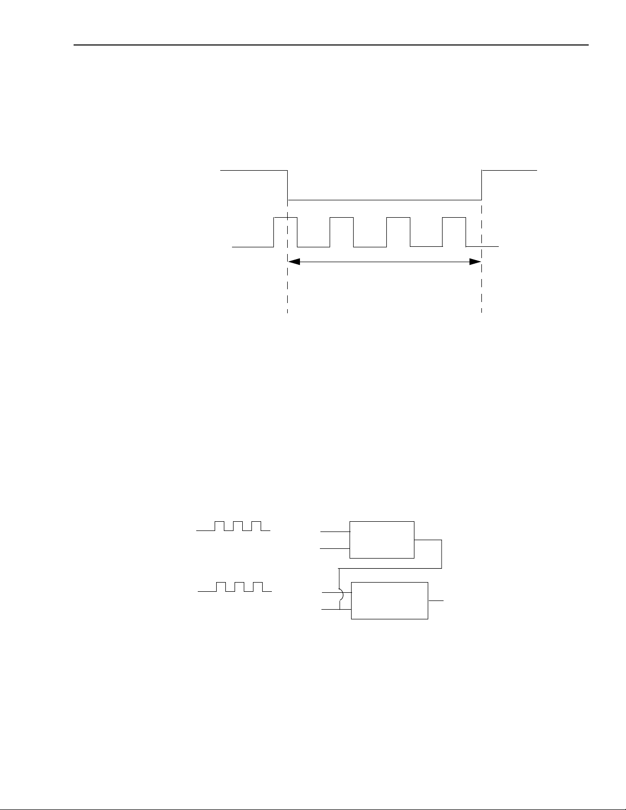
Figure 2-5 shows an example of an event counting operation. In this example, the gate type is
low level.
Figure 2-5
Example of event counting
High Level
Disables Operation
Gate Input
Signal
External C/T
Clock
Input Signal
Low Level Enables Operation
3 Events are counted while
the operation is enabled.
Event Counting
Operation Starts
Event Counting
Operation Stops
Frequency measurement
Use frequency measurement applications to measure the frequency of the signal from counter’s
external clock input source over a specified duration. In this mode, use an external C/T clock
source; refer to page 2-4 for more information on the external C/T clock source.
DriverLINX can measure the time-averaged frequency of an unknown frequency source connected to the Clock input. Frequency measurement requires two, or more counter/timers configured as gating and measurement counters. (See Figure 2-6.)
Figure 2-6
Frequency measurement using DriverLINX
Internal Clock
Unknown Frequency
Clock
Gate
Clock
Gate
Gating
Counter
Measurement
Counter
Output
Output
Page 31

2-12 Functional Description KPCI-3140 User’s Manual
The measurement counter counts the unknown frequency at its Clock input for a time interval
defined by the gating counter. DriverLINX clocks the gating counter from an internal crystal reference oscillator to produce a precise counting duration. Applications can calculate the unknown
input frequency as:
Frequency
measurementCount
----------------------------------------------------------------=
gatingCount clockPeriod×
where measurementCount is the counter value DriverLINX reads from the measurement
counter, gatingCount is the counter value the application specifies for the measurement interval
in the Service Request, and clockPeriod is the duration of the reference oscillator’s period. Refer
to DriverLINX manuals for details and conversion between counts and time.
16-Bit frequency measurement using DriverLINX
In DriverLINX 16-bit frequency measurement two counters are used as gating counters, and a
third is used as a measurement counter. Logical channels N and N+1 are gating counters, and
Channel N+2 is the measurement counter. In the Service Request, set up a polled mode task. In
RateEvent, set the mode to be FREQ, and specify a channel N and measuring period.
NOTE Channel N must be designated as Channel 0, 1, 4, or 5.
The unknown frequency signal is connected to the terminal (Channel N+2) that the application
specifies in the Service Request Clock property. Depending on the counting mode, a signal may
be connected to the Gate input. Before a frequency measurement is performed, a physical connection must be made between the Output terminal of the gating counter, Logical Channel N+1,
and the Gate terminal of the first measurement counter, Logical Channel N+2. When using multiple counter/timer channels, the application’s Service Request specifies the first gating counter/
timer (N), and DriverLINX then automatically uses consecutive counter/timer channels for the
second gating counter/timer (N+1) and the measurement counters (N+2).
32-Bit frequency measurement using DriverLINX
In DriverLINX 32-bit frequency measurement two counters are used as gating counters, and two
counters are used as a measurement counters. Logical channels N and N+1 are gating counters,
and channels N+2 and N+3 are the measurement counters.
NOTE Channel N must be designated as Channel 0 or 4.
The unknown frequency signal is connected to the terminal (Channel N+3) that the application
specifies in the Service Request Clock property. Depending on the counting mode, a signal may
be connected to the Gate input. Before a frequency measurement is performed, a physical connection must be made between the Output terminal of the gating counter, Logical Channel N+1,
and the Gate terminal of the first measurement counter, Logical Channel N+2. When using multiple counter/timer channels, the application’s Service Request specifies the first gating counter/
timer (N), and DriverLINX then automatically uses consecutive counter/timer channels for the
second gating counter/timer (N+1) and the measurement counters (N+2).
Page 32

KPCI-3140 User’s Manual Functional Description 2-13
Rate generation
Use rate generation applications to generate a continuous pulse output signal from the counter;
this application is sometimes referred to as continuous pulse output or pulse train output. You
can use this pulse output signal as an external clock to pace other operations.
While the pulse output operation is enabled, the counter outputs a pulse of the specified type and
frequency continuously. As soon as the operation is disabled, rate generation stops.
NOTE If interrupts are enabled for a C/T channel operating in rate generation
mode, the interrupt occurs when the pulse output signal changes from a
low to a high state.
The period of the output pulse is determined by the clock input signal and the external clock
divider. If you are using one counter (not cascaded), you can output pulses using a maximum
frequency of 20MHz (this is the frequency of the clock output signal). In rate generation mode,
either the internal or external C/T clock input source is appropriate depending on your application; refer to page 2-4 for more information on the C/T clock source.
Use DriverLINX software to specify a Rate Generation service request for the counter/timer, the
C/T clock source as either internal or external, the polarity of the output pulses (high-to-low
transitions or low-to-high transitions), the duty cycle of the output pulses, and the gate type that
enables the operation. Refer to page 2-7 for more information on pulse output signals and to
page 2-6 for more information on gate types.
NOTE If you want to use interrupts, it is recommended that you specify the out-
put pulse type as high to low. The interrupt occurs when the output pulse
completes.
For rate generation operations, use a duty cycle as close to 100% as
possible to output a pulse immediately. Using a duty cycle closer to 0%
acts as a pulse output delay.
Ensure that the signals are wired appropriately. Figure 2-7 shows one example of connecting a
pulse output operation to the STP-3140 screw terminal panel using user counter 0. In this example, a software gate type is used.
Figure 2-7
Connecting rate generation signals (shown for Counter Output 0;
a software gate is used)
Digital Ground
Signal
Source
User Timer Input 0
User Timer Output 0
Heater
Controller
TB1
TB2
TB3
Digital Ground
TB12
STP-3140 Panel
Page 33

2-14 Functional Description KPCI-3140 User’s Manual
Figure 2-8 shows an example of an enabled rate generation operation using an external C/T
clock source with an input frequency of 4kHz, a clock divider of 4, a high-to-low pulse type, and
a duty cycle of 75%. (The gate type does not matter for this example.) A 1kHz square wave is
the generated output. Figure 2-9 shows the same example using a duty cycle of 25%.
Figure 2-8
Example of rate generation with a 75% duty cycle
Rate Generation
Operation Starts
External C/T Clock
Input Signal (4kHz)
Pulse Output
Signal
75% Duty Cycle
If Enabled,
Interrupt Occurs.
Figure 2-9
Example of rate generation with a 25% duty cycle
Continuous Pulse
Output Operation Starts
If Enabled,
Interrupt Occurs.
If Enabled,
Interrupt Occurs.
If Enabled,
Interrupt Occurs.
External C/T Clock
Input Signal (4kHz)
Pulse Output
Signal
25% Duty Cycle
Page 34

KPCI-3140 User’s Manual Functional Description 2-15
One-shot
Use the one-shot application to generate a single pulse output signal from the counter when the
operation is triggered (determined by the gate input signal). You can use this pulse output signal
as an external gate to start other operations.
When the one-shot operation is triggered, a single pulse is output; then, the one-shot operation
stops. All subsequent clock input signals and gate input signals are ignored.
If interrupts are enabled for a C/T channel that is programmed for one-shot operation, the interrupt occurs when the pulse output signal changes from a low to a high state.
The period of the output pulse is determined by the clock input signal. In one-shot applications,
generally the internal C/T clock source is more useful than an external C/T clock source. However, if you want to be notified after a number of external events occurs, specify an external
clock source; in this case, the external clock divider specifies the number of events that occur
before the interrupt is generated. Refer to page 2-4 for more information on the C/T clock
sources.
DriverLINX can generate a variety of single pulses, delayed pulses, and strobes or one-shots.
Using DriverLINX software, specify the counter/timer as one-shot (polled pulse or strobe output), the clock source, the frequency of the output signal or the number of events that occur
before the interrupt, the polarity of the output pulse (high-to-low transition or low-to-high transition), the duty cycle of the output pulse, and the gate type to trigger the operation. Refer to
page 2-7 for more information on pulse output types and to page 2-6 for more information on
gate types.
If you want to use interrupts, it is recommended that you specify the output pulse type as high to
low. The interrupt occurs when the one-shot pulse completes.
For one-shot operations, use a duty cycle as close to 100% as possible to output a pulse immediately. Using a duty cycle closer to 0% acts as a pulse output delay.
Ensure that the signals are wired appropriately. Figure 2-10 shows one example of connecting a
pulse output operation to the STP-3140 screw terminal panel using user counter 0.
Figure 2-10
Connecting one-shot signals (shown for Counter Output 0 and Gate 0)
Heater
Controller
External
Gating
Switch
Digital Ground
C/T Output 0
Gate 0
Digital Ground
TB1
TB3
TB4
TB12
STP-3140 Panel
Page 35

2-16 Functional Description KPCI-3140 User’s Manual
Figure 2-11 shows an example of a one-shot operation using an external gate input (rising edge),
a clock output frequency of 1kHz (pulse period of 1ms), a high-to-low pulse type, and a duty
cycle of 99.99%. Figure 2-12 shows the same example using a duty cycle of 50%.
Figure 2-11
Example of one-shot application using a 99.99% duty cycle
One-Shot
Operation Starts
External Gate
Signal
Pulse Output
Signal
1ms Period
99.99% Duty Cycle
If Enabled,
Interrupt Occurs.
Figure 2-12
Example of one-shot application using a 50% duty cycle
One-Shot
Operation Starts
If Enabled,
Interrupt Occurs.
External Gate
Signal
Pulse Output
Signal
1ms Period
50% Duty
Cycle
Page 36

KPCI-3140 User’s Manual Functional Description 2-17
Repetitive one-shot
Use repetitive one-shot applications to generate a pulse output signal each time the board detects
a trigger (determined by the gate input signal). You can use this application to clean up a poor
clock input signal by changing its pulse width, then outputting it.
NOTE If interrupts are enabled for a C/T channel operating in repetitive one-
shot mode, the interrupt occurs each time the pulse output signal
changes from a low to a high state.
The period of the output pulse is determined by the clock input signal. In one-shot applications,
generally the internal C/T clock source is more useful than an external C/T clock source. However, if you want to be notified after a number of external events occurs, specify an external
clock source; in this case, the external clock divider specifies the number of events that occur
before the interrupt is generated. Refer to page 2-4 for more information on the C/T clock
sources.
Use DriverLINX service request to specify the counter/timer mode as one-shot and set pulses
property to 0 (repetitive), the C/T clock source, the frequency of the output signal or that number
of events that occur before the interrupt, the polarity of the output pulses set to zero (0), the duty
cycle of the output pulses, and the gate type to trigger the operation. Refer to page 2-7 for more
information on pulse output types and to page 2-6 for more information on gates.
NOTE If you want to use interrupts, it is recommended that you specify the out-
put pulse type as high to low. The interrupt occurs when each one-shot
pulse completes.
For repetitive one-shot operations, use a duty cycle as close to 100% as
possible to output a pulse immediately. Using a duty cycle closer to 0%
acts as a pulse output delay.
When the one-shot operation is triggered (determined by the gate input signal), a pulse is output.
When the board detects the next trigger, another pulse is output. This operation continues until
you stop the operation.
NOTE Triggers that occur while the pulse is being output are not detected by
the board.
Page 37

2-18 Functional Description KPCI-3140 User’s Manual
Figure 2-13 shows an example of a repetitive one-shot operation using an external gate (rising
edge); a clock output frequency of 1kHz (one pulse every 1ms), a high-to-low pulse type, and a
duty cycle of 99.99%. Figure 2-14 shows the same example using a duty cycle of 50%.
Figure 2-13
Example of repetitive one-shot mode using a 99.99% duty cycle
Repetitive One-Shot
Operation Starts
External Gate
Signal
Pulse Output
Signal
1ms Period
99.99% Duty Cycle
If Enabled,
Interrupt Occurs.
1ms Period
99.99% Duty Cycle
Figure 2-14
Example of repetitive one-shot mode using a 50% duty cycle
Repetitive One-Shot
Operation Starts
If Enabled,
Interrupt Occurs.
If Enabled,
Interrupt Occurs.
If Enabled,
Interrupt Occurs.
99.99% Duty Cycle
External Gate
Signal
Pulse Output
Signal
1ms Period
50% Duty
Cycle
1ms Period
50% Duty
Cycle
Page 38

KPCI-3140 User’s Manual Functional Description 2-19
Internal timer features
This subsection describes the following user internal timer features:
• Units
• Clock sources
• Gate types
• Pulse types and duty cycles
Units
KPCI-3140 boards support four 24-bit internal timer units (numbered 8 to 11).
Internal timers use an internal clock input signal and internal gate input signal, and generate an
internal clock output signal. No external connections are supported.
Each internal timer corresponds to a counter/timer (C/T) channel. Select the internal timer to use
in software by specifying its corresponding C/T channel. For example, to select internal timer 9,
specify C/T channel 9.
Clock sources
Interval timers are clocked by the internal 40MHz clock. In software, specify the clock source as
internal. Specify the frequency of the internal timer from 2.39Hz to 20MHz.
Gate types
For internal timers, use software to specify the gate type as none (software). Only a software
gate can enable an internal timer operation.
Pulse output types and duty cycles
For internal timer operations, the KPCI-3140 board generates a clock output signal that the
board uses internally to generate an interrupt condition; it is not brought out for user connection.
The pulse output type is high-to-low; it is not programmable. The pulse output signal is active
(low) for one clock pulse (25ns); the duty cycle (pulse width) is not programmable.
Interrupts
Each of the four internal timers can generate a periodic interrupt to the host computer on each
low-to-high transition of the pulse output signal. Interrupts may be enabled through DriverLINX
programming. Interrupt frequency is determined by setting of the corresponding counters and
clock source. It is equal to the output frequency of the clock that is used.
Page 39

2-20 Functional Description KPCI-3140 User’s Manual
Digital I/O features
This section describes the following features of the digital I/O subsystem:
• Digital I/O lines
• Resolution
• Operation modes
• Interrupts
Digital I/O lines
KPCI-3140 boards support 32 digital I/O lines through the digital input (DIN) and output
(DOUT) channels; the DIN and DOUT channels use the same digital I/O lines.
These lines are divided into four ports of eight: Port A, lines 0 to 7; Port B, lines 0 to 7; Port C,
lines 0 to 7; and Port D, lines 0 to 7. You can use each port for either input or output; all eight
lines within a port have the same configuration. For example, if you use Port A for input, lines 0
to 7 of Port A are configured as inputs. Likewise, if you use Port B for output, lines 0 to 7 of Port
B are configured as outputs. (See Table 2-4.)
Specify the digital I/O line to read or write in a single value digital I/O operation or a continuous
digital input operation; refer to page 2-22 for more information on digital I/O operation modes;
refer to your DriverLINX manuals for information on programming digital I/O operation.
Once the digital I/O lines have been configured using DriverLINX, and the hardware and DriverLINX software have been installed, the configuration is saved. On power up, the hardware resets
all ports to digital input, then reads the values that were saved and configures the port to its programmed value; that is, the port retains its configured value on reset.
Table 2-4
DriverLINX definition of logical channels for KPCI-3140 digital input subsystem
Logical
Channel DriverLINX Function KPCI-3140 Digital I/O Connection
0 Digital Input/Output Digital I/O Bank A 0 – 7
1 Digital Input/Output Digital I/O Bank B 0 – 7
2 Digital Input/Output Digital I/O Bank C 0 – 7
3 Digital Input/Output Digital I/O Bank D 0 – 7
4 Digital Input (interrupt register) Digital I/O Bank D 0 – 7
5 External Clock (pattern-sensitive) Digital I/O Bank D 0 – 7
6 External Clock (edge-sensitive) Digital I/O Bank D 0 – 7
7 External Trigger (pattern-sensitive) Digital I/O Bank D 0 – 7
8 External Trigger (pattern-sensitive) Digital I/O Bank D 0 – 7
Page 40

KPCI-3140 User’s Manual Functional Description 2-21
Resolution
Using DriverLINX software, specify the number of digital I/O lines to read or write at once by
specifying the resolution as 8, 16, 24, or 32. Choosing a resolution greater than 8 effectively
combines the digital I/O ports.
DriverLINX supports a software extension to logical channel addressing that allows applications
to combine adjacent logical channels into a single channel or split a logical channel into smaller
addressable parts.
In DriverLINX, “native” refers to the hardware-defined digital channel size (8 bit for
KPCI-3140). When using extended logical channel addressing, DriverLINX groups digital bits
in units defined by a size code and then assigns consecutive channel numbers starting from zero.
DriverLINX also allows masked I/O operation to a single port (8 bit). Refer to your DriverLINX
manuals for information on programming digital I/O ports.
NOTE When using size codes larger than the native addressing unit, you may
not be able to address all hardware ports if the number of available digital I/O lines is not an integral multiple of the size unit.
Table 2-5 shows the effect of resolution on the number of digital I/O lines available for each DIN
or DOUT channel.
Table 2-5
Resolution, digital I/O lines, and number of channels
Resolution Digital I/O Lines DIN or DOUT Channel
8 Port A, lines 0 to 7 Channel 0
Port B, lines 0 to 7 Channel 1
Port C, lines 0 to 7 Channel 2
Port D, lines 0 to 7 Channel 3
16 Port A and B, lines 0 to 15 combined Channel 0
Port C and D, lines 0 to 15 combined Channel 2
32 Ports A, B, C, and D, lines 0 to 31 combined Channel 0
NOTE When the resolution is greater than 8, the bit value represents the com-
bined number of digital I/O lines. For example, if the resolution is 32,
digital I/O lines 0 to 7 of Port A are represented as bits 0 to 7 of the digital value, digital I/O lines 0 to 7 of Port B are represented as bits 8 to 15
of the digital value, digital I/O lines 0 to 7 of Port C are represented as
bits 16 to 23 of the digital value, and digital I/O lines 0 to 7 of Port D
are represented as bits 24 to 31 of the digital value.
Page 41

2-22 Functional Description KPCI-3140 User’s Manual
Interrupts
The KPCI-3140 board can generate a PCI-bus interrupt when any of the eight digital I/O lines
corresponding to digital Port D (DIN element 3) changes state. This feature is useful when you
want to monitor critical signals or when you want to signal the host computer to transfer data to
or from the board. DriverLINX automatically enables the interrupt according to the Service
Request application.
NOTE When Port D is configured as input, an interrupt is generated whenever
the signal applied changes state. When port D is configured as output,
an interrupt is generated whenever the signal written to the port
changes the port value.
DriverLINX models the interrupt of this port using the DI EVENT. You
can use this DI EVENT as a pacer for background tasks or to generate
timetics (to interrupt the application). To specify when and how to generate an interrupt, fill in the DriverlINX DI EVENT parameters.
Operation modes
KPCI-3140 boards directly support the only single value digital I/O operation mode. However,
continuous digital I/O may be achieved through the DriverLINX Service Request.
• Single value operations are the simplest to use but do not allow you to check the interrupt
status. Use DriverLINX software to specify the DIN or DOUT channel, the resolution, and a
gain of 1 (the gain is ignored). Data is then read from or written to the appropriate digital I/O
lines. For a single value operation, you cannot specify a clock or trigger source.
Single value operations stop automatically when finished; you cannot stop a single value
operation.
• Continuous digital input using DriverLINX and buffer transfer allows the transfer of
data from or to the board using transfer buffers. To do this, a continuous digital I/O DriverLINX Service Request is run in the background. In the DriverLINX Service Request:
1. Specify the data to be written (digital output) or the buffer for data storage (digital Input).
2. Using the channel gain list, specify where to transfer the data from (digital output), or
transfer the data to (digital input). A digital port configured as output can be read; a
digital port configured as input cannot be written. Channel 4, which is interrupt pending
register, can only be read.
3. Specify a pacer to do the transfer. A pacer can be any counter/timer on the board or a digital event that models Port D as an interrupt source.
4. An optional start or stop trigger for the data transfer may be specified.
5. Send the Service Request to DriverLINX. DriverLINX will notify that the data is ready
or that the task is completed.
DriverLINX allows the following operation (refer to Table 2-4):
• Configuration of Digital I/O ports dynamically for either single-value or continuous
operation.
• Configuration of read/write single values to or from the ports, including different resolutions
(refer to “Resolution” page 2-21.)
• Programming of background tasks to read/write buffers.
• Use of Channel 4 to show the port interrupt pending information. This channel is read only.
• Use of Channels 5, 6, 7, and 8 to model interrupt behavior of Port D. These channels are nei-
ther writable nor readable.
Page 42

3
Installation and
Configuration
Page 43

3-2 Installation and Configuration KPCI-3140 User’s Manual
Unpacking
Open the shipping box and remove the wrapped KPCI-3140 board.
CAUTION Keep the board in its protective antistatic bag until you are ready to
install it; this minimizes the likelihood of electro-static damage.
Verify that the following items are present:
• KPCI-3140 data acquisition board
• KPCI-3140 DriverLINX Software and Documentation CD-ROM
• KPCI-3140 User’s Manual (this manual)
If an item is missing or damaged, call Keithley at:
1-888-KEITHLEY
Monday - Friday, 8:00 a.m. - 5:00 p.m., Eastern Time
An application engineer will guide you through the appropriate steps for replacing missing or
damaged items.
Installing the software
NOTE Install the DriverLINX software before installing the KPCI-3140 board.
Software options
Users of KPCI-3140 boards have the following two software options. In both cases, the software
interfaces with your system via the DriverLINX software provided with your board:
• The user can run a fully integrated data-acquisition software package such as TestPoint or
LabVIEW.
• The user can write and run a custom program in Visual C/C++, Visual Basic, or Delphi,
using the programming support provided in the DriverLINX software.
The KPCI-3140 has fully functional driver support for use under Windows 95/98/NT.
NOTE The DriverLINX Installation and Configuration Guide explains the
Otherwise, the device drivers will be more difficult to install.
DriverLINX installation process. To display this manual from your
DriverLINX KPCI-3140 CD-ROM, open the Windows Explorer, then
double click on X:\Drvlinx4\Docs\Instconf.pdf, where X = the letter of
the CD-ROM drive. Acrobat Reader must already be installed on the
other system. If necessary, you can first install Acrobat Reader directly
from the CD-ROM by double clicking X:\Acrobat\setup.exe.
Page 44

KPCI-3140 User’s Manual Installation and Configuration 3-3
DriverLINX driver software for Windows 95/98/NT
DriverLINX software, supplied by Keithley with the KPCI-3140 board, provides convenient
interfaces to configure analog and digital I/O modes without register-level programming.
Most importantly, however, DriverLINX supports those programmers who wish to create custom applications using Visual C/C++, Visual Basic, or Delphi. DriverLINX accomplishes foreground and background tasks to perform data acquisition. The software includes memory and
data buffer management, event triggering, extensive error checking, and context sensitive online help.
DriverLINX provides application developers a standardized interface to over 100 services for
creating foreground and background tasks for the following:
• Analog input and output
• Digital input and output
• Time and frequency measurement
• Event counting
• Pulse output
• Period measurement
In addition to basic I/O support, DriverLINX also provides:
• Built-in capabilities to handle memory and data buffer management.
• A selection of starting and stopping trigger events, including pre-triggering, mid-point trig-
gering and post-triggering protocols.
• Extensive error checking.
• Context-sensitive on-line help system DriverLINX is essentially hardware independent,
because its portable APIs (Application Programming Interfaces) work across various operating systems. This capability eliminates unnecessary programming when changing operating
system platforms.
TestPoint™
TestPoint is a fully featured, integrated application package that incorporates many commonly
used math, analysis, report generation, and graphics functions. The TestPoint graphical dragand-drop interface can be used to create data acquisition applications, without programming, for
IEEE-488 instruments, data acquisition boards, and RS232-485 instruments and devices.
TestPoint includes features for controlling external devices, responding to events, processing
data, creating report files, and exchanging information with other Windows programs. It provides libraries for controlling most popular GPIB instruments.
TestPoint interfaces with your KPCI-3140 board through DriverLINX, using a driver that is provided by the manufacturer.
Page 45

3-4 Installation and Configuration KPCI-3140 User’s Manual
LabVIEW
LabVIEW is a fully featured graphical programming language used to create virtual instrumentation. It consists of an interactive user interface, complete with knobs, slide switches, graphs,
strip charts, and other instrument panel controls. Its data-driven environment uses function
blocks that are virtually wired together and pass data to each other. The function blocks, which
are selected from palette menus, range from arithmetic functions to advanced acquisition, control, and analysis routines. Also included are debugging tools, help windows, execution highlighting, single stepping, probes, and breakpoints to trace and monitor the data flow execution.
LabVIEW can be used to create professional applications with minimal programming.
A Keithley VI palette provides standard virtual instruments (VIs) for LabVIEW that interface
with your KPCI-3140 board through DriverLINX. The needed driver is provided on your DriverLINX CD-ROM.
™
Installing DriverLINX
Refer to the instructions on the Read this first sheet and the manuals on the DriverLINX
CD-ROM, both shipped with your board, for information on installing and using DriverLINX.
Installing application software and drivers
Installing the TestPoint software and driver
The DriverLINX driver for TestPoint is provided as part of the TestPoint software. The driver
therefore installs automatically when you install TestPoint.
You can install TestPoint application software at any time—before or after installing DriverLINX and the KPCI-3140 board. For TestPoint installation instructions, consult the manual provided with TestPoint.
NOTE Before using TestPoint with the KPCI-3140 version of DriverLINX,
check with Keithley to ensure that your version of TestPoint is
compatible with DriverLINX.
Installing the LabVIEW software and driver
A DriverLINX driver for LabVIEW is provided on your DriverLINX CD-ROM. The LabVIEW
driver does not install automatically when you install DriverLINX and your board. You must first
install the LabVIEW application program, then install the DriverLINX driver. Access the LabVIEW driver installation routine by starting setup.exe on the DriverLINX CD-ROM, then selecting LabVIEW
Consult the manual provided with LabVIEW for installation instructions.
™
Support from the Install These DriverLINX components screen.
Page 46

KPCI-3140 User’s Manual Installation and Configuration 3-5
Installing the KPCI-3140 board
To install the board, check the system requirements, set up the computer, select an available 32bit or 64-bit PCI expansion slot, and insert the board into the slot. The following subsections
describe how to perform these steps.
To install the board, perform the following steps:
• Check the system requirements, described in Section 1, “Overview”
• Set up the computer, described on page 3-5
• Select an expansion slot, described on page 3-5
• Insert the board into any available 32-bit or 64-bit PCI expansion slot in your computer,
described on page 3-6
NOTE The KPCI-3140 is factory-calibrated and requires no further adjustment
prior to installation.
Setting up the computer
CAUTION To prevent electro-static damage that can occur when handling elec-
tronic equipment, use a ground strap or similar device when performing this installation procedure.
1. Turn off the computer.
2. Turn off all peripherals (printer, modem, monitor, and so on) connected to the computer.
3. Unplug the computer and all peripherals.
4. Remove the cover from you computer. Refer to your computer’s user manual for
instructions.
Selecting an expansion slot
1. Select a 32-bit or 64-bit PCI expansion slot.
PCI slots are shorter than ISA or EISA slots and are usually white or ivory. Commonly, three
PCI slots (one of which may be a shared ISA/PCI slot) are available. If an ISA board exists
in the shared slot, you cannot use the slot for a PCI board; likewise if a PCI board exists in
the shared slot, you cannot use the slot for an ISA board.
2. Remove the cover plate from the selected expansion slot. Retain the screw that held it in
place; you will use it later to install the board.
Page 47

3-6 Installation and Configuration KPCI-3140 User’s Manual
Inserting the board in the computer
1. To discharge any static electricity, hold the wrapped board in one hand while placing your
other hand firmly on a metal portion of the computer chassis.
2. Carefully remove the antistatic packing material from the board. (We suggest that you save
the original packing material in the unlikely event that your board requires servicing in the
future.)
3. Hold the board by its edges and do not touch any of the components on the board.
4. Position the board so that the cable connectors are facing the rear of the computer, as shown
in Figure 3-1.
Figure 3-1
Inserting a KPCI-3140 board in the computer
KPCI-3140
Series Board
PCI Expansion Slot
Bus Connector
Rear of Computer
5. Carefully lower the board into the PCI expansion slot using the card guide to properly align
the board in the slot. When the bottom of the board contacts the bus connector, gently press
down on the board until it clicks into place.
CAUTION Do not force the board into place. Moving the board from side to side
during installation may damage the bus connector. If you encounter
resistance when inserting the board, remove the board and try again.
6. Secure the board in place at the rear panel of the system unit using the screw removed from
the slot cover.
Page 48

KPCI-3140 User’s Manual Installation and Configuration 3-7
Configuring the board to work with DriverLINX
After physically installing the board, turn on and reboot the computer. The DriverLINX Plug
and Play Wizard screen appears. Run the Wizard immediately by following the progressive
instructions on the screen.
If you do not run the Wizard immediately, it will not appear the next time you reboot. You must
then restart the Wizard from a batch file, as follows:
1. Open the Windows Explorer.
2. Double click on X:\DrvLINX4\Help\kpci3140.bat, where X = the letter of the drive on
which you installed DriverLINX.
The Wizard appears.
NOTE You can also start this batch file directly from the CD-ROM by double
clicking on Y:\DrvLINX4\Help\kpci3140.bat, where Y = the drive letter
of your CD-ROM drive.
Using the DriverLINX configuration panel
To configure a KPCI-3140 board (logical device), use the DriverLINX icon in the Windows
Control Panel application. The DriverLINX Configuration Panel displays a tree list of all the
installed DriverLINX drivers on you system and the configured Logical Devices under each
driver.
NOTE If you are running Windows NT, Windows NT’s security features require
that users installing or configuring device drivers log on under an
administrative account.
Use the Configuration Panel to instruct DriverLINX to initialize the hardware into a custom configuration of input and output ports and default output values. This may be useful if you connect
you hardware’s outputs to external devices that expect high logic signals, rather than the default
low logic signals, as their starting state.
Pushing the Configure... button on the DriverLINX Configuration Panel displays a Configure
DriverLINX Device property page for configuring the selected Logical Device. The tabbed dialog box has a page for each Logical Subsystem that your board supports. Select and complete
each property page to configure the Logical Device.
1. On the Device Property Page, enter the required fields:
2. At this point, you may select OK and accept default initialization, or select another Property
Page.
3. If you select the Counter/Timer Property page, you may view the clock source frequency:
• Resolution — shows the master internal clock frequency that the counter/timers use. All
models have a 40MHz clock source for pacing input/output tasks and counter/timer
functions.
• Interrupt — DriverLINX disables this property. Windows automatically determines the
interrupt level for the KPCI-3140 board.
4. If you select the Digital Input Property page, you may configure the Digital I/O ports.
• Channels — shows the available Logical Channels for digital input and selects the Logi-
cal Channel for the Configuration properties.
• Resolution — shows the master internal clock frequency that the counter/timers use. All
models have a 40MHz clock source for pacing input/output tasks and counter/timer
functions.
Page 49

3-8 Installation and Configuration KPCI-3140 User’s Manual
NOTE DriverLINX disables the Configuration group if the board’s digital
channels do not support software reprogramming as inputs or outputs.
5. If you select the Digital Output Property page, you may define output values for initializing
the ports.
• Channels — shows the available Logical Channels for digital output and selects the Log-
ical Channel for the Initialization properties.
• Value — specifies the output value DriverLINX uses to initialize the port selected in the
Channels list box. DriverLINX ignores this property if Initialize is not checked.
• Initialize — when checked, this property indicates that DriverLINX should automati-
cally initialize this channel as specified in the Value property.
6. To Statistically Initialize Digital Output Ports (initialize Logical Channel 0 with all bits at
logic high), on the Digital Output Property page:
• Select “0 (bits 0 - 7)” in the Channels list box.
• Enter “255” (DEC) or “0xFF: (Hex) in the Initialization Value edit box.
• Click the Initialize check box.
• Repeat this procedure for every Logical Channel that requires user-defined initialization.
7. After completing all Property Pages, press OK to save your configuration.
For programming your counter/timers with DriverLINX, refer to DriverLINX Counter/Timer
Programming Guide on the DriverLINX CD ROM.
You can use DriverLINX to verify board operation:
1. To physically initialize the KPCI-3140, select Device/Initialize from the main menu in Learn
DriverLINX.
2. The first time the KPCI-3140 is initialized, or after a configuration change, DriverLINX runs
a diagnostic program to verify the operation and accuracy of the configuration settings.
You are now ready to make I/O connections. Refer to Section 2 for descriptions of common I/O
connections for KPCI-3140 boards.
Checking the combined board and DriverLINX installations
Before making any connections to the board, check whether DriverLINX and your board are
installed correctly and working together properly. Refer to Section 4 and the DriverLINX
manuals.
Try starting the DriverLINX KPCI-3140 Test Panel. Proceed as follows:
1. In the Start menu, click Programs.
2. Find the DriverLINX → Test Panels folder, under which you should find the KPCI-3140
Test Panel entry.
3. Click on the Test Panel entry.
4. If a KPCI-3140 board is the only board in your computer installed under DriverLINX or if
the DriverLINX Test Panel lists the KPCI-3140 board under Driver Selection, then DriverLINX and your board are installed properly and are working together.
5. If you cannot initially run the Test Panel, refer to Section 5.
After DriverLINX and your board are installed properly and working together, continue with
installation and wiring.
Page 50

KPCI-3140 User’s Manual Installation and Configuration 3-9
Attaching the STP-3140 screw terminal panel
Before you can wire signals, you first need to attach the STP-3140 screw terminal panel to the
KPCI-3140 board. Connector J1 on the screw terminal panel brings out all of the digital and
counter/timer signals from connector J1 on the KPCI-3140 board; cable CAB-305 connects connector J1 on the screw terminal panel to the KPCI-3140 board.
Figure 3-2 illustrates how to attach the STP-3140 screw terminal panel to the KPCI-3140 board.
Figure 3-2
Attaching the STP-3140 screw terminal panel to the KPCI-3140 board
KPCI-3140
Board
J1
CAB-305 Cable
J1
STP-3140 Screw
Terminal Panel
Figure 3-3 shows the layout of the STP-3140 screw terminal panel.
Figure 3-3
Layout of the STP-3140 screw terminal panel
J1, 68-Pin Connector
TB17
R6
TB21
R5
TB12
TB16
R3
TB9
R4
TB13
R1
TB4
TB1
R2
TB8
TB5
TB28
TB32
R7
TB20
TB25
R8
TB24
TB29
TB72
TB53TB63
TB43
TB52TB62
TB33
TB42
Page 51

3-10 Installation and Configuration KPCI-3140 User’s Manual
Screw terminals
Table 3-1 lists the screw terminal assignments for the STP-3140 screw terminal panel.
Table 3-1
Screw terminal assignments on the STP-3140 screw terminal panel
TB #J1Pin # Signal description TB #J1Pin # Signal description
1 68 Digital Ground 2 67 C/T Clock Input 0
3 66 C/T Clock Output 0 4 65 C/T Gate Input 0
5 34 Digital Ground 6 33 C/T Clock Input 1
7 32 C/T Clock Output 1 8 31 C/T Gate Input 1
9 64 C/T Gate Input 2 10 63 C/T Clock Output 2
11 62 C/T Clock Input 2 12 61 Digital Ground
13 30 C/T Gate Input 3 14 29 C/T Clock Output 3
15 28 C/T Clock Input 3 16 27 Digital Ground
17 42 Digital Ground 18 41 C/T Clock Input 4
19 40 C/T Clock Output 4 20 39 C/T Gate Input 4
21 8 Digital Ground 22 7 C/T Clock Input 5
23 6 C/T Clock Output 5 24 5 C/T Gate Input 5
25 38 C/T Gate Input 6 26 37 C/T Clock Output 6
27 36 C/T Clock Input 6 28 35 Power Ground
29 4 C/T Gate Input 7 30 3 C/T Clock Output 7
31 2 C/T Clock Input 7 32 1 +5V Output
33 - Shield 34 60 Digital I/O Port A, Line 0
35 26 Digital I/O Port A, Line 1 36 59 Digital I/O Port A, Line 2
37 25 Digital I/O Port A, Line 3 38 58 Digital I/O Port A, Line 4
39 24 Digital I/O Port A, Line 5 40 57 Digital I/O Port A, Line 6
41 23 Digital I/O Port A, Line 7 42 56 Digital Ground
43 - Shield 44 55 Digital I/O Port B, Line 0
45 21 Digital I/O Port B, Line 1 46 54 Digital I/O Port B, Line 2
47 20 Digital I/O Port B, Line 3 48 53 Digital I/O Port B, Line 4
49 19 Digital I/O Port B, Line 5 50 52 Digital I/O Port B, Line 6
51 18 Digital I/O Port B, Line 7 52 22 Digital Ground
53 - Shield 54 51 Digital I/O Port C, Line 0
55 17 Digital I/O Port C, Line 1 56 50 Digital I/O Port C, Line 2
57 16 Digital I/O Port C, Line 3 58 49 Digital I/O Port C, Line 4
59 15 Digital I/O Port C, Line 5 60 48 Digital I/O Port C, Line 6
61 14 Digital I/O Port C, Line 7 62 47 Digital Ground
63 - Shield 64 46 Digital I/O Port D, Line 0
65 12 Digital I/O Port D, Line 1 66 45 Digital I/O Port D, Line 2
67 11 Digital I/O Port D, Line 3 68 44 Digital I/O Port D, Line 4
69 10 Digital I/O Port D, Line 5 70 43 Digital I/O Port D, Line 6
71 9 Digital I/O Port D, Line 7 72 13 Digital Ground
Page 52

KPCI-3140 User’s Manual Installation and Configuration 3-11
Resistors
As shown in Figure 3-3, the STP-3140 has eight resistor locations which correspond to the eight
clock input signals. Table 3-2 lists the clock input signals and the resistors to which they
correspond.
Table 3-2
Clock input signals and resistor use
Clock Input Signal Resistor
Clock Input 0 R1
Clock Input 1 R2
Clock Input 2 R3
Clock Input 3 R4
Clock Input 4 R5
Clock Input 5 R6
Clock Input 6 R7
Clock Input 7 R8
Wiring signals
Wiring recommendations
By default, the STP-3140 is shipped with 0Ω resistors in these resistor locations. If you are
using high-frequency external clock input signals (greater than 1MHz), you may want to change
the resistor values on both the KPCI-3140 board and STP-3140 panel. Refer to page 3-11 for
more information on changing resistor values.
To avoid electrical damage, ensure that power is turned off to the computer and to any attached
devices before wiring signals to the STP-3140 screw terminal panel.
When first installing the board, try wiring an external clock and scope to counter/timer 0, and a
digital input to digital input Port A. Then run DriverLINX Test Panel to verify that the board is
operating properly. Once you have determined that the board is operating properly, wire the signals according to your application’s requirements.
NOTE When using clock sources greater than 1MHz, it is recommended that
use counter/timers 0 to 3. This is the CE configuration of the board.
When connecting external clock signals greater than 1MHz, it is recommended that you insert a
resistor to ground for the corresponding counter/timer clock input signal on the KPCI-3140
board. This resistor is used in parallel with the 1kΩ resistor on the board. The appropriate value
for the user-supplied resistor depends on your application, the frequency of the clock input signal, and the cable length. You should also terminate the corresponding signal on the STP-3140
panel by replacing the 0Ω resistor on the STP-3140 with a resistor of an appropriate matching
value.
Page 53

3-12 Installation and Configuration KPCI-3140 User’s Manual
For example, if you are connecting an external clock signal to clock input signal 0 on the
KPCI-3140 board and running the board at its maximum clock input frequency, it is recommended that you insert a 110Ω resistor to ground on the board for the clock input signal 0, and
replace the 0Ω resistor in location R1 on the STP-3140 panel with a 100Ω resistor for proper termination.
Figure 3-4 shows the location of the resistors on the KPCI-3140 board. Figure 3-3 shows the
location of the resistors on the STP-3140 screw terminal panel.
Figure 3-4
Location for user-supplied resistors on the KPCI-3140 board
C/T 0
C/T 3
C/T 4
C/T 7
KPCI-3140
In addition, keep the following general recommendations in mind when wiring signals to the
STP-3140 screw terminal panel:
• Use individually shielded twisted-pair wire (size 14 to 26 AWG) when using the KPCI-3140
board in highly noisy electrical environments.
• Separate power and signal lines by using physically different wiring paths or conduits.
• To avoid noise, do not locate the STP-3140 screw terminal panel and cabling next to sources
that produce high electro-magnetic fields, such as large electric motors, power lines, solenoids, and electric arcs, unless the signals are enclosed in a metal shield.
• Connect the shields to one end only (either at the STP-3140 or at the signal source).
NOTE If you are using a screw terminal panel other than the STP-3140, refer
to Appendix A for additional wiring considerations.
Connecting counter/timer signals
The KPCI-3140 board with the STP-3140 screw terminal panel provides user counter/timers that
you can use to perform the following operations:
• Event counting
• Frequency measurement
• Pulse output (rate generation, one-shot, and repetitive one-shot)
This section describes how to connect counter/timer signals to perform these operations.
Page 54

KPCI-3140 User’s Manual Installation and Configuration 3-13
Connecting event counting signals
Figure 3-5 shows one example of connecting event counting signals to the STP-3140 screw ter-
minal panel using user counter 0. In this example, rising clock edges are counted while the gate
is active.
Figure 3-5
Connecting event counting applications to the STP-3140 screw terminal panel
(shown for Clock Input 0 and External Gate 0)
Signal Source
External
Gating
Switch
Digital Ground
User Clock Input 0
Gate 0
Digital Ground
Shield
TB1
TB2
TB4
TB12
TB33
STP-3140 Panel
Figure 3-6 shows another example of connecting an event counting application to the STP-3140
screw terminal panel using user counter 0. In this example, a software gate is used to start the
event counting operation.
Figure 3-6
Connecting event counting applications to the STP-3140 screw terminal panel without
an External Gate Input (shown for Clock Input 0)
Signal Source
Digital Ground
User Clock Input 0
Shield
TB1
TB2
TB33
STP-3140 Panel
Page 55

3-14 Installation and Configuration KPCI-3140 User’s Manual
Figure 3-7 shows an example of how to externally cascade two counters to perform an event
counting operation using user counters 0 and 2. Note that you can also internally cascade
counters using software; if you internally cascade the counters, you do not need to make the
external cascading connections. Note also that this example shows the use of an external gate;
however, this connection is not required.
Figure 3-7
Cascading counters (shown for event counting using Counters 0 and 2
and External Gate 0)
Signal Source
External
Gating
Switch
Digital Ground
User Clock Input 0
Gate 0
Digital Ground
Shield
TB3
TB11
TB33
STP-3140 Panel
TB1
TB2
TB4
TB12
User Counter
Output 0
User Clock
Input 2
Connecting frequency measurement signals
In DriverLINX frequency measurement, the application specifies the Logical Channel N, of the
gating counter in the Service Request. The unknown frequency signal is connected to the terminal the application specifies in the Service Request Clock property. Depending on the counting
mode, a signal may be connected to the Gate input. Before a frequency measurement is performed, a physical connection must be made between the Output terminal of the gating counter,
Logical Channel N, and the Gate terminal of the first measurement counter, Logical Channel
N+1. When using multiple counter/timer channels, the application’s Service Request specifies
the gating counter/timer, and DriverLINX then automatically uses consecutive counter/timer
channels for the measurement counter(s).
You can connect a pulse of a known duration (such as a one-shot output of another user counter)
to the external gate input, as shown in Figure 3-8. In this configuration, the frequency of the
clock input is the number of counts divided by the period of the external gate input.
Page 56

KPCI-3140 User’s Manual Installation and Configuration 3-15
Figure 3-8
Connecting frequency measurement applications to the STP-3140 screw terminal panel
(shown for Clock Input 0 and External Gate 0)
Digital Ground
User Clock Input 0
Signal Source
Gate 0
User Counter
Output 2
Shield
TB1
TB2
TB4
TB10
TB33
STP-3140 Panel
Connecting pulse output signals
Figure 3-9 shows one example of connecting a pulse output application to the STP-3140 screw
terminal panel using user counter 0. Other combinations of signals can be used.
Figure 3-9
Connecting pulse output applications to the STP-3140 screw terminal panel
(shown for Counter Output 0 and Gate 0)
Heater
Controller
External
Gating
Switch
Digital Ground
User Counter Output 0
Gate 0
Digital Ground
Shield
TB1
TB3
TB4
TB12
TB33
STP-3140 Panel
Page 57

3-16 Installation and Configuration KPCI-3140 User’s Manual
Figure 3-10 shows an example of how to externally cascade two counters to perform a rate gen-
eration operation using user counters 0 and 2. Note that you can also internally cascade counters
using software; if you internally cascade the counters, you do not have to make the external cascading connections. In this example, counter 2 gate is logic high.
Figure 3-10
Cascading counters (shown for rate generation using Counters 0 and 2
and External Gate 0)
Signal Source
External
Gating
Switch
Digital Ground
User Clock Input 0
Gate 0
Digital Ground
Shield
TB3
TB11
TB33
STP-3140 Panel
TB1
TB2
TB4
TB12
User Counter
Output 0
User Clock
Input 2
Figure 3-11 shows an example of how to externally cascade two counters to perform a one-shot
operation using user counters 0 and 2. Note that you can also internally cascade counters using
software; if you internally cascade the counters, you do not have to make the external cascading
connections. In this example, counter 0 gate is logic high.
Figure 3-11
Cascading counters (shown for one-shot using Counters 0 and 2 and External Gate 2)
Signal Source
One-Shot
Trigger
Digital Ground
User Clock Input 0
Gate 2
Digital Ground
Shield
TB1
TB2
TB3
TB4
TB9
TB11
TB12
TB33
STP-3140 Panel
User Counter
Output 0
User Clock
Input 2
Page 58

KPCI-3140 User’s Manual Installation and Configuration 3-17
Connecting digital input signals
Figure 3-12 shows how to connect a digital input signal (lines 0 and 1 of digital Port A, in this
case) to the STP-3140 screw terminal panel.
Figure 3-12
Connecting digital inputs to the STP-3140 screw terminal panel
(Lines 0 and 1, Port A shown)
TTL Inputs
Connecting digital output signals
Figure 3-13 shows how to connect a digital output signal (line 0 of digital Port B, in this case) to
the STP-3140 screw terminal panel.
Figure 3-13
Connecting digital outputs to the STP-3140 screw terminal panel (Line 0, Port B shown)
0 Out = LED On
500Ω
+
5V
-
Digital I/O Port B 0
Shield
Digital I/O Port A 0
Digital I/O Port A 1
TB33
TB34
TB35
STP340 Panel
TB44
Digital Ground
TB52
STP340 Panel
Page 59

4
Testing the Board
Page 60

4-2 Testing the Board KPCI-3140 User’s Manual
Using DriverLINX KPCI-3140 test panel for hardware testing
The test panels are small applications programs within DriverLINX that allow you to perform
limited data acquisition functions. You can use the panels to do tasks such as:
• Generate Sine, Square and Triangle waves using the SST Signal Generator
• Output pulse and strobe
• Set and read digital input and output bits on your board
The DriverLINX KPCI-3140 Test Panel is useful for:
• Testing the KPCI-3140 DriverLINX installation and configuration
• Verifying signal inputs to your KPCI-3140 board
• Sending test signals to external devices
• Providing a realistic example of a working KPCI-3140 for study
DriverLINX KPCI-3140 test panel procedure
To start up and use the DriverLINX KPCI-3140 Test Panel, perform the following steps:
1. At the Windows Start Program menu, select DriverLINX.
2. From the DriverLINX menu, select Utilities.
3. From the Utilities menu, select Test Panels.
4. From the Test Panels, select KPCI-3140 Panel.
5. After the test panel starts, perform the necessary setup for the KPCI-3140 board.
6. To set up and perform an operation, click the appropriate input and output panels.
7. To obtain information on the setup and performance of an operation, use the DriverLINX
online help.
8. When you finish using the test panel, select File Exit to terminate the program.
NOTE This utility allows you to verify basic operations on the board; however,
it does not support all of the board’s features.
Page 61

5
Troubleshooting
Page 62

5-2 Troubleshooting KPCI-3140 User’s Manual
General checklist
Should you experience problems using the KPCI-3140 board, please follow these steps:
1. Read all the appropriate sections of this manual. Make sure that you have added any Read
This First information to your manual and that you have used this information.
2. Check your distribution disk for a README file and ensure that you have used the latest
installation and configuration information available.
3. Check that your system meets the requirements stated in this manual.
4. Check that you have installed your hardware properly using the instructions in this manual.
5. Check that you have installed and configured DriverLINX properly using the instructions in
the DriverLINX manuals that come with the DriverLINX software.
If your KPCI-3140 board is not operating properly, use the information in this section to help
you isolate the problem. If the problem appears serious enough to require technical support,
refer to page 5-6 for information on how to contact an applications engineer.
If you encounter a problem with a KPCI-3140 board, use the instructions in this section to isolate the cause of the problem before calling Keithley for technical support.
Using the DriverLINX event viewer
The DriverLINX Event Viewer displays the Windows system event log. Applications and hardware drivers make entries in the system event log to assist in predicting and troubleshooting
hardware and software problems.
DriverLINX uses the event log to report problems during driver loading or unexpected system
errors. The event log can assist in troubleshooting resource conflicts and DriverLINX configuration errors. If you are having trouble configuring or initializing a Logical Device, check the
event log for information from the DriverLINX driver.
Using the DriverLINX Event Viewer, you can view, save and e-mail DriverLINX event log
entries under Windows 95/98 or Windows NT. DriverLINX event log entries can help you or
technical support troubleshoot data-acquisition hardware and software problems.
Device initialization error messages
During device initialization, DriverLINX performs a thorough test of all possible subsystems on
the KPCI-3140 board as well as the computer interface. If DriverLINX detects any problems or
unexpected responses, it reports an error message to help isolate the problem. The device initialization error messages fall into three basic categories:
• “Device not found” — Board address does not match hardware setting or conflicts with
another board. Verify the board’s address settings. Also, do not confuse hexadecimal with
decimal addresses in the DriverLINX Device Configure dialog box.
• “Invalid IRQ level” — Selected level does not match hardware setting, conflicts with
another board’s IRQ levels, or is dedicated to the computer’s internal functions (COM port,
disk drive controller, network adapter, etc.).
• “Hardware does not match configuration” — Operating mode/range switch or jumper set-
ting does not match selection(s) made in the DriverLINX Device Configuration dialog box.
Page 63

KPCI-3140 User’s Manual Troubleshooting 5-3
Problem isolation
If you encounter a problem with a KPCI-3140 board, perform the following steps to determine
whether the problem is in the computer, in the KPCI-3140 board, or in the I/O circuitry:
1. Remove power connections to the host computer.
2. Unplug the accessory connector(s) or cable(s) from the KPCI-3140 board(s), keeping the
connections intact on the accessory or expansion board(s).
3. Remove the KPCI-3140 board(s) from the computer and visually check for damage. If a
board is obviously damaged, refer to page 5-7 for information on returning the board.
4. With the KPCI-3140 board(s) out of the computer, check the computer for proper operation.
Power up the computer and perform any necessary diagnostics.
5. When you are sure that the computer is operating properly, remove computer power again,
and install a KPCI-3140 board that you know is functional. Do not make any I/O
connections.
6. Apply computer power and check operation with the functional KPCI-3140 board in place.
This test checks the computer accessory slot. If you are using more than one KPCI-3140
board, check the other slots you are using.
7. If the accessory slots are functional, check the I/O hookups. Connect the accessory and
expansion boards, one at a time, and check operation.
8. If operation is normal, the problem is in the KPCI-3140 board(s) originally in the computer.
Try the KPCI-3140 board(s) one at a time in the computer to determine which is faulty. Use
the troubleshooting information in the next section to try to isolate the problem.
9. If you cannot isolate the problem using the general instructions here, refer to Appendix C,
“Systematic Problem Isolation” for a more detailed problem isolation scheme.
10. If you cannot isolate the problem after further investigation, refer to page 5-6 for instructions
on getting technical support.
Page 64

5-4 Troubleshooting KPCI-3140 User’s Manual
Troubleshooting table
If you still experience problems, try using the information in to isolate and solve the problem. If
you cannot identify the problem, refer to Section “Technical support” on page 5-6.
Table 5-1
Troubleshooting problems
Symptom Possible Cause Possible Solution
Board does not
respond.
Intermittent
operation.
Board does not
interrupt.
Data appears to
be invalid.
Computer does
not boot.
System lockup. Board is not seated properly. Check that the slot in which your KPCI-3140 board is located is a PCI
The board configuration is incorrect. Check the configuration of your device driver to ensure that the board
name and type are correct.
The board is incorrectly aligned in a
PCI expansion slot.
The board is damaged. Contact Keithley Instruments.
Loose connections or vibrations
exist.
The board is overheating. Check environmental and ambient temperature; consult the board’s
Electrical noise exists. Check your wiring and either provide better shielding or reroute
Counter/timer, interval timer, or
digital I/O port is not configured
properly.
An open connection exists. Check your wiring and fix any open connections.
A transducer is not connected to the
channel being read.
The interrupt level is unacceptable. An interrupt conflict exists in your system. The most common interrupt
Board is not seated properly. Check that the slot in which your KPCI-3140 board is located is a PCI
The power supply of the computer
is too small to handle all the system
resources.
Check that the slot in which your KPCI-3140 board is located is a PCI slot
and that the board is correctly seated in the slot.
Check your wiring and tighten any loose connections or cushion vibration
sources.
specifications in the Appendix of this manual and the documentation
provided by your computer manufacturer for more information.
unshielded wiring.
Check the parameters configured in DriverLINX for the KPCI-3140
board.
Check the transducer connections.
conflict occurs with a PCI device and a device that is plugged into the ISA
bus. To correct this problem, change the interrupt setting (usually by
changing a jumper) on the ISA device.
An interrupt conflict can also occur if a PCI device was not designed to
share interrupts. To resolve this problem, select a different interrupt for
each PCI slot in the PCI BIOS. To do this, enter the system BIOS
program; this is usually done by pressing the DEL key when re-booting
your system. Once in the system BIOS, enter the PCI/PnP BIOS setup,
and select a unique interrupt for each PCI slot. The PCI BIOS assigns the
interrupt; the device on the PCI bus does not have control over the
interrupt assignment.
Some network devices do not share interrupts. If you still have an interrupt
conflict, try removing the network device, installing the KPCI-3140 board
and re-booting the system, then reinserting the network device.
slot, that the board is correctly seated in the slot, and that the board is
secured in the slot with a screw.
Check the power requirements of your system resources and, if needed,
get a larger power supply; consult the board’s specifications in the
Appendix of this manual.
slot, that the board is correctly seated in the slot, and that the board is
secured in the slot with a screw.
Page 65

KPCI-3140 User’s Manual Troubleshooting 5-5
Testing the board and host computer
To isolate the problem to the KPCI-3140 board or to the host computer, use the following steps.
CAUTION Removing a board with the power ON can cause damage to your
board and/or computer.
1. Turn the power to the host computer OFF, and remove power connections to the computer.
2. While keeping connections to accessories intact, unplug the cable to the main I/O connector
of the KPCI-3140 board.
3. Remove the board from the computer and visually check for damage. If a board is obviously
damaged, refer to “Technical support” for information on returning the board.
4. With the KPCI-314 0 board out of the computer, check the computer for proper operation.
Power up the computer and perform any necessary diagnostics.
At this point, if you have another KPCI-3140 board that you know is functional, you can test the
slot and I/O connections using the instructions in the next section. If you do not have another
board, call technical support.
Testing the accessory slot and I/O connections
When you are sure that the computer is operating properly, test the computer accessory slot and
I/O connections using another KPCI-3140 board that you know is functional. To test the computer accessory slot and the I/O connections, follow these steps:
1. Remove computer power again, and install a KPCI-3140 board that you know is functional.
Do not make any I/O connections.
2. Turn computer power ON and check operation with the functional board in place. This test
checks the computer accessory slot. If you were using more than one board when the problem occurred, use the functional board to also test the other slot.
3. If the accessory slots are functional, use the functional board to check the I/O connections.
Reconnect and check the operation of the I/O connections, one at a time.
4. If operation fails for an I/O connection, check the individual inputs one at a time for shorts
and opens.
5. If operation remains normal to this point, the problem is in the KPCI-3140 board(s) originally in the computer. If you were using more than one board, try each board one at a time in
the computer to determine which is faulty.
6. If you cannot isolate the problem using the general instructions here, refer to Appendix C,
“Systematic Problem Isolation” for a more detailed problem isolation scheme.
7. If you cannot isolate the problem, refer to the following paragraph for information on obtaining technical support.
Page 66

5-6 Troubleshooting KPCI-3140 User’s Manual
Technical support
Before returning any equipment for repair, call Keithley for technical support at:
1 - 888 - KEITHLEY
Monday - Friday, 8:00 a.m. - 5:00 p.m., Eastern Time
An applications engineer will help you diagnose and resolve your problem over the telephone.
Please make sure you have the following information available before calling the factory for
technical support:
KPCI-3140 Board
Configuration
Computer Manufacturer
Operating System DOS version
Software Package Name
Compiler
(if applicable)
Accessories Type
Model
Serial #
Revision code
Base address setting
Interrupt level setting
Number of channels
CPU type
Clock speed (MHz)
KB of RAM
Video system
BIOS type
Windows version
Windows mode
Serial #
Version
Invoice/Order #
Language
Manufacturer
Version
Type
Type
Type
Type
Type
Type
Type
____________________
____________________
____________________
____________________
____________________
____________________
____________________
____________________
____________________
____________________
____________________
____________________
____________________
____________________
____________________
____________________
____________________
____________________
____________________
____________________
____________________
____________________
____________________
____________________
____________________
____________________
____________________
____________________
____________________
____________________
Page 67

KPCI-3140 User’s Manual Troubleshooting 5-7
Returning equipment to Keithley
If a telephone resolution is not possible, the applications engineer will issue you a Return
Material Authorization (RMA) number and ask you to return the equipment. Include the RMA
number with any documentation regarding the equipment.
When returning equipment for repair, include the following information:
• Your name, address, and telephone number.
• The invoice or order number and date of equipment purchase.
• A description of the problem or its symptoms.
• The RMA number on the outside of the package.
Repackage the equipment, using the original anti-static wrapping, if possible, and handle it with
ground protection. Ship the equipment to:
ATTN.: RMA# _______
Repair Department
Keithley Instruments, Inc.
28775 Aurora Road
Cleveland, Ohio 44139
Telephone 1-888-KEITHLEY
FAX (440) 248-6168
NOTE If you are submitting your equipment for repair under warranty, you
must include the invoice number and date of purchase.
To enable Keithley to respond as quickly as possible, you must include
the RMA number on the outside of the package.
Page 68

A
Specifications
Page 69

A-2 Specifications KPCI-3140 User’s Manual
KPCI-3140 specifications
Table A-1 lists the specifications for the C/T subsystems on the KPCI-3140 boards.
Table A-1
C/T subsystem specifications
Feature Specifications
Number of counter/timers 8
Clock Inputs
Input type:
Input load:
Threshold voltage
Counter/Timers 0, 1, 2, 3:
Counter/Timers 4, 5, 6, 7:
Input sensitivity:
Input hysteresis:
Input current (V
= 0V):
in
Input current (Vin = 5V):
Minimum pulse width:
Maximum frequency:
Termination
Counter/Timers 0, 1, 2, 3:
Counter/Timers 4, 5, 6, 7:
Gate Inputs
Input type:
Input load:
High-level input voltage:
Low-level input voltage:
Hysteresis:
High-level input current:
Low-level input current:
Minimum pulse width:
Termination:
Counter Outputs for Channels 0, 1, 2, 3
Output driver:
Termination:
Output driver high voltage:
Output driver low voltage:
Pseudo-differential, rising-edge sensitive
1 AM26C32
1
0.5V
0.98V
±200mV
60mV
0
1kΩ
25ns high and low (sampled by 40MHz)
19.9MHz typical
1,2
100Ω
1kΩ resistor to ground
3
Schmitt trigger, level sensitive
1 HCT14 (TTL)
2.0V minimum
0.8V maximum
0.4V (minimum); 1.5V (maximum)
1.0µA
-1.0µA
25ns high and low (sampled by 40MHz)
22kΩ resistor pullup to +5V
1.2V peak-to-peak
1
100Ω
1
2.6V maximum at 100Ω
1.2V maximum at 100Ω
Counter Outputs for Channels 4, 5, 6, 7
Output driver:
Output driver high voltage:
Output driver low voltage:
Termination:
1
This value accommodates high-frequency clock signals.
2
If you want to use low-frequency clock signals you can clip the 100Ω resistors in locations R9 (counter/timer 0), R14
(counter/timer 1), R19 (counter/timer 2), and R27 (counter/timer 3).
3
You can install a 110Ω resistor to ground on the board in parallel with the 1kΩ resistor to give 100Ω termination.
ALS244 (TTL)
3.0V maximum at 100Ω
1.6V maximum at 100Ω
100Ω series resistor;
301Ω pull-down resistor to ground (75Ω)
Page 70

KPCI-3140 User’s Manual Specifications A-3
Table A-2 lists the specifications for the DIN/DOUT subsystems on the KPCI-3140 boards.
Table A-2
DIN/DOUT subsystem specifications
Feature
Ports A, B, and C
Specifications
Port D
Specifications
Number of lines 8 per port 8
Direction bidirectional
Termination 22kΩ resistor pullup to +5V; 22Ω series resistor
Inputs
Input type:
Input load:
High-level input voltage:
Low-level input voltage:
High-level input current:
Low-level input current:
Minimum Pulse Width
High:
Low:
Level sensitive
2 FCT2574 (TTL)
2.0V minimum
0.8V maximum
3µA
-3µA
Not Applicable
Not Applicable
Level sensitive
3 FCT2574 (TTL)
2.0V minimum
0.8V maximum
4.5µA
4.5µA
66ns (2 PCI clocks)
66ns (2 PCI clocks)
1
1
Outputs
Output driver:
Output driver high voltage:
Output driver low voltage:
1
The minimum pulse width applies only to interrupt-on-change detection. Pulses less than the minimum may not be
detected as a change.
FCT2574 (TTL)
2.4V minimum (IOH = -15mA);
0.5V maximum (IOL = 12mA)
Table A-3 lists the power, physical, and environmental specifications for the KPCI-3140 boards.
Table A-3
Power, physical, and environmental specifications
Feature Specifications
Power
+5V (±0.25V)
- 5V
+12V
-12V
405mA + output current nominal
not used
not used
not used
Physical
Dimensions:
PCI short card
6.875 inches (length) by 4.2 inches (height);
174mm (length) by 106mm (height)
Weight:
4 ounces (113.4 grams)
Environmental
Operating temperature range:
Storage temperature range:
Relative humidity:
0° to 70°C
-25° to 85°C
To 95%, noncondensing
Page 71

A-4 Specifications KPCI-3140 User’s Manual
Table A-4 lists the specifications for the 68-pin connector on the board.
Table A-4
68-Pin connector specifications
Feature Specifications
Connector part number: AMP 68-pin, 0.05 Subminiature D, #749621-7
Shielded enclosure with jack screws: AMP 750752-1
Recommended shielded cable: Madison, 28 GA, Twisted Pair, #68KDK00029
Page 72

B
Connector Pin
Assignments
Page 73

B-2 Connector Pin Assignments KPCI-3140 User’s Manual
Table B-1 lists the pin assignments of connector J1 on the KPCI-3140 board.
Table B-1
Connector J1 pin assignments on the KPCI-3140 board
Pin Number Signal Description Pin Number Signal Description
01 +5V Output 02 C/T Clock Input 7
03 C/T Clock Output 7 04 C/T Gate Input 7
05 C/T Gate Input 5 06 C/T Clock Output 5
07 C/T Clock Input 5 08 Digital Ground
09 Digital I/O Port D, Line 7 10 Digital I/O Port D, Line 5
11 Digital I/O Port D, Line 3 12 Digital I/O Port D, Line 1
13 Digital Ground 14 Digital I/O Port C, Line 7
15 Digital I/O Port C, Line 5 16 Digital I/O Port C, Line 3
17 Digital I/O Port C, Line 1 18 Digital I/O Port B, Line 7
19 Digital I/O Port B, Line 5 20 Digital I/O Port B, Line 3
21 Digital I/O Port B, Line 1 22 Digital Ground
23 Digital I/O Port A, Line 7 24 Digital I/O Port A, Line 5
25 Digital I/O Port A, Line 3 26 Digital I/O Port A, Line 1
27 Digital Ground 28 C/T Clock Input 3
29 C/T Clock Output 3 30 C/T Gate Input 3
31 C/T Gate Input 1 32 C/T Clock Output 1
33 C/T Clock Input 1 34 Digital Ground
35 Power Ground 36 C/T Clock Input 6
37 C/T Clock Output 6 38 C/T Gate Input 6
39 C/T Gate Input 4 40 C/T Clock Output 4
41 C/T Clock Input 4 42 Digital Ground
43 Digital I/O Port D, Line 6 44 Digital I/O Port D, Line 4
45 Digital I/O Port D, Line 2 46 Digital I/O Port D, Line 0
47 Digital Ground 48 Digital I/O Port C, Line 6
49 Digital I/O Port C, Line 4 50 Digital I/O Port C, Line 2
51 Digital I/O Port C, Line 0 52 Digital I/O Port B, Line 6
53 Digital I/O Port B, Line 4 54 Digital I/O Port B, Line 2
55 Digital I/O Port B, Line 0 56 Digital Ground
57 Digital I/O Port A, Line 6 58 Digital I/O Port A, Line 4
59 Digital I/O Port A, Line 2 60 Digital I/O Port A, Line 0
61 Digital Ground 62 C/T Clock Input 2
63 C/T Clock Output 2 64 C/T Gate Input 2
65 C/T Gate Input 0 66 C/T Clock Output 0
67 C/T Clock Input 0 68 Digital Ground
Page 74

KPCI-3140 User’s Manual Connector Pin Assignments B-3
Table B-2 lists the screw terminal assignments for the STP-3140 screw terminal panel.
Table B-2
Screw terminal assignments on the STP-3140 screw terminal panel
TB # J1 Pin # Signal Description TB # J1 Pin # Signal Description
01 68 Digital Ground 02 67 C/T Clock Input 0
03 66 C/T Clock Output 0 04 65 C/T Gate Input 0
05 34 Digital Ground 06 33 C/T Clock Input 1
07 32 C/T Clock Output 1 08 31 C/T Gate Input 1
09 64 C/T Gate Input 2 10 63 C/T Clock Output 2
11 62 C/T Clock Input 2 12 61 Digital Ground
13 30 C/T Gate Input 3 14 29 C/T Clock Output 3
15 28 C/T Clock Input 3 16 27 Digital Ground
17 42 Digital Ground 18 41 C/T Clock Input 4
19 40 C/T Clock Output 4 20 39 C/T Gate Input 4
21 8 Digital Ground 22 7 C/T Clock Input 5
23 6 C/T Clock Output 5 24 5 C/T Gate Input 5
25 38 C/T Gate Input 6 26 37 C/T Clock Output 6
27 36 C/T Clock Input 6 28 35 Power Ground
29 4 C/T Gate Input 7 30 3 C/T Clock Output 7
31 2 C/T Clock Input 7 32 1 +5V Output
33 - Shield 34 60 Digital I/O Port A, Line 0
35 26 Digital I/O Port A, Line 1 36 59 Digital I/O Port A, Line 2
37 25 Digital I/O Port A, Line 3 38 58 Digital I/O Port A, Line 4
39 24 Digital I/O Port A, Line 5 40 57 Digital I/O Port A, Line 6
41 23 Digital I/O Port A, Line 7 42 56 Digital Ground
43 - Shield 44 55 Digital I/O Port B, Line 0
45 21 Digital I/O Port B, Line 1 46 54 Digital I/O Port B, Line 2
47 20 Digital I/O Port B, Line 3 48 53 Digital I/O Port B, Line 4
49 19 Digital I/O Port B, Line 5 50 52 Digital I/O Port B, Line 6
51 18 Digital I/O Port B, Line 7 52 22 Digital Ground
53 - Shield 54 51 Digital I/O Port C, Line 0
55 17 Digital I/O Port C, Line 1 56 50 Digital I/O Port C, Line 2
57 16 Digital I/O Port C, Line 3 58 49 Digital I/O Port C, Line 4
59 15 Digital I/O Port C, Line 5 60 48 Digital I/O Port C, Line 6
61 14 Digital I/O Port C, Line 7 62 47 Digital Ground
63 - Shield 64 46 Digital I/O Port D, Line 0
65 12 Digital I/O Port D, Line 1 66 45 Digital I/O Port D, Line 2
67 11 Digital I/O Port D, Line 3 68 44 Digital I/O Port D, Line 4
69 10 Digital I/O Port D, Line 5 70 43 Digital I/O Port D, Line 6
71 9 Digital I/O Port D, Line 7 72 13 Digital Ground
Page 75

B-4 Connector Pin Assignments KPCI-3140 User’s Manual
Table B-3 lists the screw terminal assignments for the STP-68 screw terminal panel.
Table B-3
Screw terminal assignments for the STP-68 screw terminal panel
TB # J1 Pin # Signal Description TB # J1 Pin # Signal Description
01 01 +5V Output 02 02 C/T Clock Input 7
03 03 C/T Clock Output 7 04 04 C/T Gate Input 7
05 05 C/T Gate Input 5 06 06 C/T Clock Output 5
07 07 C/T Clock Input 5 08 08 Digital Ground
09 09 Digital I/O Port D, Line 7 10 10 Digital I/O Port D, Line 5
11 11 Digital I/O Port D, Line 3 12 12 Digital I/O Port D, Line 1
13 13 Digital Ground 14 14 Digital I/O Port C, Line 7
15 15 Digital I/O Port C, Line 5 16 16 Digital I/O Port C, Line 3
17 17 Digital I/O Port C, Line 1 18 18 Digital I/O Port B, Line 7
19 19 Digital I/O Port B, Line 5 20 20 Digital I/O Port B, Line 3
21 21 Digital I/O Port B, Line 1 22 22 Digital Ground
23 23 Digital I/O Port A, Line 7 24 24 Digital I/O Port A, Line 5
25 25 Digital I/O Port A, Line 3 26 26 Digital I/O Port A, Line 1
27 27 Digital Ground 28 28 C/T Clock Input 3
29 29 C/T Clock Output 3 30 30 C/T Gate Input 3
31 31 C/T Gate Input 1 32 32 C/T Clock Output 1
33 33 C/T Clock Input 1 34 34 Digital Ground
35 35 Power Ground 36 36 C/T Clock Input 6
37 37 C/T Clock Output 6 38 38 C/T Gate Input 6
39 39 C/T Gate Input 4 40 40 C/T Clock Output 4
41 41 C/T Clock Input 4 42 42 Digital Ground
43 43 Digital I/O Port D, Line 6 44 44 Digital I/O Port D, Line 4
45 45 Digital I/O Port D, Line 2 46 46 Digital I/O Port D, Line 0
47 47 Digital Ground 48 48 Digital I/O Port C, Line 6
49 49 Digital I/O Port C, Line 4 50 50 Digital I/O Port C, Line 2
51 51 Digital I/O Port C, Line 0 52 52 Digital I/O Port B, Line 6
53 53 Digital I/O Port B, Line 4 54 54 Digital I/O Port B, Line 2
55 55 Digital I/O Port B, Line 0 56 56 Digital Ground
57 57 Digital I/O Port A, Line 6 58 58 Digital I/O Port A, Line 4
59 59 Digital I/O Port A, Line 2 60 60 Digital I/O Port A, Line 0
61 61 Digital Ground 62 62 C/T Clock Input 2
63 63 C/T Clock Output 2 64 64 C/T Gate Input 2
65 65 C/T Gate Input 0 66 66 C/T Clock Output 0
67 67 C/T Clock Input 0 68 68 Digital Ground
Page 76

C
Systematic
Problem Isolation
Page 77

C-2 Systematic Problem Isolation KPCI-3140 User’s Manual
Problem isolation schemes
If you were unable to isolate the problem by using Section 5, then try to isolate the problem systematically using the schemes detailed in this Appendix.
For clarity, the systematic problem isolation procedure is divided into seven schemes, each of
which checks for, eliminates, and/or resolves problem causes. Each scheme consists of a flowchart and, in most cases, an amplified written procedure. The numbers of flowchart blocks are
keyed to the numbers of written steps.
For simplicity, your problem is assumed to have only one cause. One particular scheme may not
alone isolate this cause. Rather, performance of several schemes in series may be required to
analyze your problem. One scheme may eliminate potential causes from further consideration,
then direct you to another scheme(s) that ultimately isolates the problem. You need perform only
those schemes to which you are directed.
If the cause of your problem appears to be outside the scope of the systematic isolation procedure, the procedure directs you to call Keithley for help.
The seven problem isolation schemes are as follows:
• Scheme A checks for three basic system problems.
• Scheme B checks DriverLINX installation and board recognition by DriverLINX.
• Scheme C addresses application software issues.
• Scheme D addresses apparent expansion slot malfunctions and attempted remedies.
• Scheme E addresses potential external connection problems.
• Scheme F addresses apparently malfunctioning board(s).
• Scheme G verifies that earlier schemes have found and addressed the problem.
Start the systematic isolation procedure at the next section, entitled “Problem isolation Scheme
A: basic system), unless you have been directed otherwise in this manual.
CAUTION Always turn OFF your computer and any external circuits
connected to the KPCI-3140 board before removing or replacing the
board. Removing or replacing a board with the power ON can
damage the board, the computer, the external circuit, or all three.
Handle the board at the mounting bracket, using a grounded wrist
strap. Do not touch the circuit traces or connector contacts.
In the following procedure, the term “board” always refers to a KPCI-3140 board. The procedure never directs you to install or remove any type of board other than a KPCI-3140 board.
The logic used in the systematic problem isolation schemes assumes that the problem has only
one cause. Therefore, once a cause is found and corrected, the reader is instructed to reassemble
the system and verify proper operation.
Each individual scheme in this procedure, except for Scheme A, is designed to be used only if
called for by other schemes or procedures. If you attempt to use schemes independently, you
lose the benefits of systematic problem isolation.
Page 78

KPCI-3140 User’s Manual Systematic Problem Isolation C-3
Problem isolation Scheme A: basic system
In Scheme A, you start the systematic problem isolation procedure. You remove your
KPCI-3140 board(s) and check for apparent damage. If the board looks okay, you check the
independent functionality of your computer. If the computer is okay, you check the expansion
slots that held your KPCI-3140 board(s).
Follow these instructions as you perform Scheme A:
1. Remove and inspect the KPCI-3140 board(s) for damage as follows:
a. Shut down Windows 95/98/NT and turn off power to the host computer.
b. Turn off power to all external circuits and accessories connected to the KPCI-3140
board(s) that is installed.
c. Disconnect screw terminal accessories from your KPCI-3140 board(s).
d. Remove the KPCI-3140 boards from the computer, making note of the socket(s) in which
the board(s) was installed. (If more than one KPCI-3140 board is installed, remove all
boards and note which board was in which socket.)
e. Visually inspect the removed KPCI-3140 board(s) for damage.
2. Based on the results of step 1, do the following:
• If the board(s) you removed is obviously damaged, then repair or replace the board.
Refer to “Technical support” for information on returning the board for repair or replacement. Skip to “Problem isolation Scheme G: verification of problem solution.”
• If the board(s) you removed is not obviously damaged, then continue with step 3 and
check for host computer malfunction.
3. Check if the computer functions satisfactorily by itself. Proceed as follows:
a. Place the board(s) that you removed from the computer in an electrostatically safe loca-
tion. Do not reinstall it.
b. Turn on power to the host computer.
c. Perform all needed diagnostics to determine whether your computer hardware and oper-
ating system are functioning properly.
4. Based on the results of step 3, do one of the following:
• If you find no computer or operating system malfunctions in step 3, then the problem
likely lies elsewhere; take action as follows:
– If you do not have another KPCI-3140 board that you know is working properly, read
the instructions in “Technical support.” Then contact Keithley for help in isolating the
cause of your problem.
– If you have another KPCI-3140 board that you know is working properly, then con-
tinue with step 5.
• If you find computer or operating system malfunctions in step 3, do the following:
a. Determine the cause of the computer hardware or operating system malfunctions.
b. Fix the computer hardware or operating system malfunctions.
c. Assume that fixing the malfunctions has solved your problem, and skip to “Problem
isolation Scheme G: verification of problem solution.”
Page 79

C-4 Systematic Problem Isolation KPCI-3140 User’s Manual
5. Determine the PCI resources detected by your computer before any KPCI-3140 boards are
installed. Proceed as follows:
a. Shut down Windows 95/98/NT and turn off power to the host computer.
b. Insert a blank diskette, or any diskette that you are sure is unbootable, into the A: drive.
c. Turn on the computer and allow it to start the boot cycle.
The boot cycle stalls at a text screen listing system characteristics and resources and saying at the bottom: Non-system disk or disk error. Replace and press any key when
ready.
NOTE This system characteristics and resources screen is normally displayed
only fleetingly during the boot cycle. Having an unbootable diskette in
your computer automatically stops the boot cycle at this screen, allowing for convenient viewing. This is not harmful to your computer. The
more common approach—using the P
AUSE key to pause the boot cycle at
this screen—requires fast reflexes with some systems.
d. Note the displayed list of PCI devices under a heading something like PCI device list-
ing… If you have a printer, print the screen by pressing the PRINT SCREEN key.
e. Remove the diskette and allow the boot cycle to finish.
6. Install a good board—a KPCI-3140 board that you know is fully functional—as follows:
a. Shut down Windows 95/98/NT and turn off power to the host computer.
b. Install the good board in the slot from which you removed the potentially faulty board in
step 1. Refer to Section 3 for board installation instructions.
NOTE If you removed more than one board in step 1, install only one good
board in only one expansion slot.
Do not connect any external circuits to the board at this point.
7. Again determine the PCI resources detected by your computer, after the KPCI-3140 board is
installed. Windows 95 Plug and Play should find and configure the new board as a PCI
resource if all of the following are true:
• The board functions properly as a PCI device.
• The contacts of the expansion slot in which the OK board is installed are in good
condition.
• The OK board is seated properly in the expansion slot.
8. Do the following, as you did in step 5:
a. Insert an unbootable diskette.
b. Turn on the computer and allow the boot cycle to stall at the Non-system disk or disk
error… message.
c. Again, note the displayed list of PCI devices. A new device should be listed, likely as an
unidentified peripheral. If your resource listing includes PCI slot numbers, the slot number for the new device should match the number of the slot in which your board is
installed.
d. Remove the diskette and allow the boot cycle to finish.
9. If you removed KPCI-3140 boards from other PCI slots in step 1, then repeat steps 6 and 7
with the good board in each of these other slots.
Page 80

KPCI-3140 User’s Manual Systematic Problem Isolation C-5
10. Based on the results of steps 5 through 8, do one of the following:
a. If the good board is recognized as a PCI component in all slots tested, then the PCI slots
are apparently satisfactory. DriverLINX may not be installed correctly and/or the board
may not be properly configured. Continue with “Problem isolation Scheme B:
installation.”
b. If the good board is not recognized as a PCI component in a slot(s), then the PCI slot con-
nector(s) is suspect. Continue with “Problem isolation Scheme D: expansion slot
connectors.”
Problem isolation Scheme B: installation
In Scheme B, you check whether DriverLINX and your board are installed correctly and work
together properly. A proper start of the DriverLINX Digital I/O Panel utility means that the combined DriverLINX/board installation is okay. If the installation is not okay, you try to diagnose
and fix the problem, ultimately reinstalling DriverLINX and the board if necessary.
NOTE This is not a stand-alone procedure. Use it only when it is called for by
another procedure.
Follow these instructions as you perform Scheme B:
1. Try starting the DriverLINX Digital I/O Panel. Proceed as follows:
a. In the Start menu, click Programs.
b. Find the DriverLINX → Test Panels folder, under which you should find the DIO
Panel entry.
c. Click on the DIO Panel entry.
2. Based on the results of Step 1, select one of the following:
• Case A — If both of the following statements are true, then skip to step 16; DriverLINX
and your board are installed properly and are working together.
– A KPCI-3140 board is the only board in your computer installed under DriverLINX.
– The DriverLINX Digital I/O Panel appears with the KPCI-3140 board listed under
Driver Selection.
• Case B — If all three of the following statements are true, then skip to step 16; Driver-
LINX and your board are installed properly and are working together.
– More than one type of board is installed in your computer under DriverLINX.
– The DriverLINX Digital I/O Panel initially appears, but perhaps with any or all of the
following differences: 1) tiny buttons located at the right side of the Driver Selection
text box and/or the Device Selection text box; 2) a different board driver under
Driver Selection; 3) a different device number under Device Selection; 4) different
tabs at the top of the screen.
– To change the tabs at the top of the screen, use the tiny buttons next to the text boxes:
1) select the board driver under Driver Selection to be KPCI-3140 and 2) select the
correct device number under Device Selection, which is 0 if only one KPCI-3140
board is installed.
• Case C — If neither of the two scenarios above apply—neither Case A nor Case B, then
continue with step 3; there may be a problem with the DriverLINX installation and/or the
board configuration.
Page 81

C-6 Systematic Problem Isolation KPCI-3140 User’s Manual
3. Select the next step in Scheme B based on the criteria given in the following alternatives:
• If you have already reconfigured or reinstalled DriverLINX and the board, yet still cannot
successfully start the Digital I/O Panel, then the cause of your problem may be outside
the scope of these diagnostics. Read the instructions in “Technical support” and then
contact Keithley for help in isolating the cause of your problem.
• If you have not yet tried to fix the combined DriverLINX/board problem, then continue
with step 4.
4. See if and how your KPCI-3140 board is listed in the Windows Device Manager. Proceed as
follows:
a. Right-click the My Computer icon on your desktop.
b. On the menu that appears, click Properties.
c. On the System Properties dialog box that appears, click the Device Manager tab. The
Device Manager appears.
d. In the Device Manager look for a DriverLINX drivers item.
e. If you find a DriverLINX drivers item, click the + sign to the left of this item. A second
level list may appear with the specific model number of your KPCI-3140 board. More
than one KPCI-3140 board may be listed here if you installed more than one KPCI-3140
board.
f. Select your next action based on the criteria given in the following alternatives:
• If a board is recognized as a device under DriverLINX but is not configured to work
with DriverLINX, then the board is normally listed with a large exclamation point
over it. If you find a KPCI-3140 board listed with an exclamation point over it, keep
the Device Manager open and go directly to step 5. Skip substeps 4g through 4j.
• If a board is recognized as a device under DriverLINX and is configured to work with
DriverLINX, then the board is listed without the large exclamation point over it.
However, this is not by itself a sufficient indication in at least one situation. Therefore, if you find that all of your KPCI-3140 boards are listed in the Device Manager
without exclamation points, do as follows:
– Leave the Device Manager open for now.
– Continue with substeps 4g through 4j, in which you open and check the Driver-
LINX Configuration Panel.
• If the list of devices in the Device Manager includes an ? Other Devices item, also
click the + sign to the left of this item. If a KPCI-3140 board is listed under ? Other
Devices, then keep the Device Manager open and go directly to step 5. Skip substeps
4g through 4j.
• If one or more of your KPCI-3140 boards is not listed anywhere in the Device Manager, then keep the Device Manager open and go directly to step 5. Skip substeps 4g
through 4j.
g. In the Start menu, click Programs.
h. Find the DriverLINX folder and under it click DriverLINX Configuration Panel.
The DriverLINX Configuration Panel appears.
i. Inspect the DriverLINX Configuration Panel.
• If you see the following on the screen for a KPCI-3140 board, then the board is recognized as a device under DriverLINX but is not properly configured:
– Keithley KPCI-3140 is listed under DriverLINX.
– The amplifier icon next to Keithley KPCI-3140 board listing is colored yellow.
– The specific board part number(s) of the unconfigured Keithley KPCI-3140
board(s) is listed under Keithley KPCI-3140.
– The lamp icon next to the specific board part number is uncolored.
Page 82

KPCI-3140 User’s Manual Systematic Problem Isolation C-7
• If you see the following on the screen for a KPCI-3140 board, then the board is rec-
ognized as a device under DriverLINX and is properly configured:
– Your Keithley KPCI-3140 Board is listed under DriverLINX.
– The amplifier icon next to Keithley KPCI-3140 listing is colored pale gray.
– A device number—for example, Device0 (or Device1, Device2, etc.)—is listed
under your Keithley KPCI-3140 board, instead of a specific board part number.
– The lamp icon next to the device number is colored green.
j. Leave the DriverLINX Configuration Panel open for now and continue with step 5.
5. Based on the results of step 4, do one of the following:
• If your board is properly installed and configured, your inability to run the Digital I/O
Panel may be due to an improperly installed component of DriverLINX. Skip to step 9,
and begin uninstalling, then reinstalling DriverLINX and the board.
• If one of your KPCI-3140 boards is apparently recognized by DriverLINX but is listed in
the Device Manager under DriverLINX with a large exclamation point, then try configuring it with the DriverLINX Configuration Panel. Skip to step 7.
• If one of your KPCI-3140 boards is listed under ? Other Devices, or is listed in the
Device Manager at multiple places, then the installation is faulty. Skip to step 9 and begin
uninstalling, then reinstalling DriverLINX and the board.
• If your board is not listed at all in the Device Manager, there are apparently issues other
than the combined DriverLINX/board installation. Continue with step 6.
6. Select the next step in Scheme B based on the criteria given in the following alternatives:
• If you are performing Scheme B independently as an installation check, then non-
installation issues must apparently be resolved before you can successfully run your
board. Starting at “Problem isolation Scheme A: basic system,” proceed through the
systematic problem isolation procedure.
• If you are performing Scheme B as part of the systematic problem isolation procedure,
then you should have seen your board listed in the device manager at this point in the
procedure. The cause of your problem may be outside the scope of these diagnostics.
Read the instructions in “Technical support,” and then contact Keithley for help in isolating the cause of your problem.
7. Try to reconfigure your board using the DriverLINX configuration panel, which you opened
in step 4 and should still be open. Proceed as follows:
a. In the DriverLINX Configuration Panel, select an unconfigured KPCI-3140 board by
clicking on its part number. An unconfigured KPCI-3140 board may be identified as
follows:
• The specific board part number of the unconfigured Keithley KPCI-3140 board is
listed under Keithley KPCI-3140.
• The lamp icon next to the specific board part number is uncolored.
• The amplifier icon next to Keithley KPCI-3140 is colored yellow.
b. Click the Configure button. The Select Logical Device dialog box appears.
c. Select your next action based on the criteria given in the following alternatives:
• If only one KPCI-3140 board is installed, a default device number of 0 in the text box
is correct. Click OK.
• If other KPCI-3140 boards are installed and configured and have been assigned
device numbers, then type in a device number for the board you are configuring—the
next, unassigned number in the numbering sequence. Then click OK.
d. The Configure DriverLINX Device dialog box appears, as well as the Device Manager.
e. No changes in the Device dialog box changes are normally required. Click OK.
f. If a Device Change message appears, then click OK.
Page 83

C-8 Systematic Problem Isolation KPCI-3140 User’s Manual
g. If more than one unconfigured board was found in the DriverLINX Configuration
Manager in step 4, configure the additional boards now. Repeat substeps 7a through 7e
for each remaining unconfigured board.
h. Close out all programs and reboot your computer to complete the configuration process.
i. Open and check the Device Manager as you did in step 4. Your KPCI-3140 board(s)
should now be listed under the DriverLINX with no exclamation mark over it.
j. Open and check the DriverLINX Configuration panel as you did in step 4. If you success-
fully configured your board(s), you should now see the following listed below Keithley
KPCI-3140. Refer back to step 4.
• Instead of a specific board part number(s), there should now be a device number(s)—
for example, Device0.
• The lamp icon next to the device number(s) should be colored green.
8. Based on the results of step 7, do one of the following:
• If the board was successfully configured, return to step 1 and retry starting the Digital I/O
Panel.
• If the board was not successfully configured, continue with step 9 and begin uninstalling,
then reinstalling DriverLINX and the board.
9. Remove all KPCI-3140 boards physically.
NOTE You should remove all KPCI-3140 boards before reinstalling the
KPCI-3140 version of DriverLINX, because the installation order is
DriverLINX first, board second. If a KPCI-3140 board is present, physically or in the computer list of devices, driver installation difficulties
may occur.
10. Proceed as follows:
a. Turn off the computer.
b. Remove all KPCI-3140 boards from their computer expansion slots.
CAUTION Wear a grounded wrist strap to avoid electrostatic damage to the
board. Do not touch board components or conductors when handling the board.
11. Remove all KPCI-3140 boards from the list of devices in your system. If your operating system is Windows 95/98, remove the KPCI-3140 boards using the Windows 95/98 Device
Manager, as follows:
a. Shut down and turn off the computer.
b. Open the Device Manager by right clicking the My Computer icon, clicking Properties
on the menu that appears, then clicking the Device Manager tab. A list of installed
devices appears.
c. Select your next step based on the criteria given in the following alternatives:
• If the Device Manager lists a DriverLINX drivers item, click the + sign to the left of
this item. A second level list may appear with the specific model number of your
KPCI-3140 board. More than one KPCI-3140 board may be listed if you previously
installed more than one KPCI-3140 board. Alternatively, if a previously installed
board is not properly recognized by DriverLINX, it may not be listed here or may be
listed with a large exclamation point over it.
• If the Device Manager lists an ? Other Devices item, also click the + sign to the left
of this item. You should not, but could, find a KPCI-3140 board listed under this item
if it is not properly recognized by DriverLINX.
Page 84

KPCI-3140 User’s Manual Systematic Problem Isolation C-9
d. Select any one of the KPCI-3140 boards that you find in the Device Manager, wherever
you find it.
e. At the bottom of the list of devices, click Remove.
f. On the Confirm Device Removal dialog box that appears, click OK. The board is
removed from the list of devices.
g. If more than one KPCI-3140 board was listed in the Device Manager, or if the same
board was listed in more than one place, then repeat substeps d, e, and f of step 10 until
no KPCI-3140 boards are listed anywhere in the Device Manager.
12. Uninstall only the KPCI-3140 version of DriverLINX from your system using the Windows
95/98/NT Add/Remove Programs feature. Proceed as follows:
a. In the Start menu of Windows 95/98/NT, click Settings → Control Panel.
b. In the Control Panel that appears, click Add/Remove Programs.
c. In the Add/Remove Programs Properties dialog box that appears, select DriverLINX for
Keithley KPCI-3140.
NOTE Uninstall only DriverLINX for Keithley KPCI-3140. If additional
DriverLINX versions are installed, leave them installed.
d. At the bottom of the Add/Remove Programs Properties dialog box, click Add/Remove
and then follow the remainder of the Windows uninstall prompts.
CAUTION During the course of an uninstall procedure, you will typically be
asked if you wish to uninstall certain files that may be shared by
other programs. In such cases, always click No. Mistakenly
uninstalling files needed by other programs causes serious problems.
Mistakenly keeping files causes no harm, and some uninstalled files
may be overwritten anyway when you subsequently reinstall
DriverLINX.
13. Reinstall DriverLINX, referring to the brief DriverLINX installation instructions on the
Read This First sheet that was shipped with your KPCI-3140 board and is also provided on
the CD-ROM containing this manual. Make sure that DriverLINX installs smoothly and
completely.
14. Reinstall the board(s).
CAUTION Wear a grounded wrist strap to avoid electrostatic damage to the
board. Do not touch board components or conductors when
handling the board.
NOTE If you are performing Scheme B independently as an installation check,
then reinstall all boards that you removed in step 9. If you are performing Scheme B as part of the systematic problem isolation procedure,
then reinstall only the good board that you began using near the end of
Scheme A.
15. Proceed as follows:
a. Shut down and turn off the computer.
b. Install the board(s) in its expansion slot(s), following this brief procedure in Section 3 of
the manual.
c. Turn on and reboot the computer.
d. Run the procedure for configuring the board to work with DriverLINX, in Section 3.
e. Return to step 1 and run the installation check again.
Page 85

C-10 Systematic Problem Isolation KPCI-3140 User’s Manual
16. You arrived at this step from step 2, after successfully starting the Digital I/O Panel. Select
your next action based on the criteria given in the following alternatives:
• If you are performing Scheme B independently as an installation check, then Driver-
LINX and your KPCI-3140 board are installed correctly. Return to Section 3 and finish
installing your data acquisition system.
• If you performed Scheme B as part of the systematic problem isolation procedure AND
arrived at this point after reconfiguring the board or reinstalling DriverLINX and the
board, then go to “Problem isolation Scheme G: verification of problem solution.”
• If you performed Scheme B as part of the systematic problem isolation procedure AND
arrived at this point without performing any remedial efforts, then your problem must lie
elsewhere. Go to “Problem isolation Scheme C: application software” and check for
application software issues.
Problem isolation Scheme C: application software
In Scheme C, you check for bugs in custom application software, assuming that you can access
the source code. Alternatively, you check for compatibility and installation issues in commercial
application software. In Scheme A, you temporarily installed a KPCI-3140 board that is known
to be good in place of a KPCI-3140 board that you removed from the computer. This
substitution, still in place, eliminates possible board I/O problems during Scheme C. You now
perform I/O tests using your application software. You debug custom code, if necessary, and
recheck.
NOTE This is not a stand-alone procedure. Use it only when it is called for by
another procedure.
Follow these instructions as you perform Scheme C:
1. Perform the procedure outlined in the “General-purpose digital I/O software test,” found
later in this appendix.
2. Based on the results of the “General-purpose digital I/O hardware test,” do one of the
following:
• If your software appears not to be working properly with your digital I/O, skip to step 4.
• If your software appears to be working properly with your digital I/O, continue.
3. Select the next step in Scheme C based on the criteria given in the following alternatives:
• If you reached this point without modifying the custom software or reinstalling the com-
mercial software—if you experienced no problems in the tests at any point—then the
problem you originally experienced must lie elsewhere. Go to “Problem isolation
Scheme E: user wiring” and check your external connections.
• If you reached this point by having to modify the custom software or reinstall the com-
mercial software—if you no longer experience problems in the tests—then assume that
you have solved the original problem. Go to “Problem isolation Scheme G: verification
of problem solution” and verify that the problem is solved.
4. You arrived at this point because one of the I/O software tests failed. Select the next step in
Scheme C based on the criteria given in the following alternatives:
• If your applications program is a proven program—potentially a commercial program
that you cannot modify—then the software may be installed incorrectly or perhaps is
incompatible with DriverLINX.
• If your applications program is a custom program that can be modified—the source code
is available—then continue.
5. Check and debug the source code as necessary.
Page 86

KPCI-3140 User’s Manual Systematic Problem Isolation C-11
6. At this point, you have presumably found and corrected some program bugs. Select the next
step in Scheme C based on the criteria given in the following alternatives:
• If both of the following statements are true, then the cause of your problem may be out-
side the scope of these diagnostics. Read the instructions in “Technical support,” and
then contact Keithley for help in isolating the cause of your problem.
– You are at this point after having debugged the source code at least once and after
having failed the I/O software tests at least a second time.
– You have tried to find more code bugs after two or more I/O test failures and cannot
find any more bugs.
• If none or only one of the above statements are true, then continue with step 7, and selec-
tively redo I/O software tests.
7. Select your next step in Scheme C based on the criteria given in the following alternatives:
• If you have done the input software test at least once AND your software did not pass the
input software test the last time, then return to step 1 and redo that test.
• If you have done the input software test at least once AND your software passed the input
software test the last time, then assume that you do not need to repeat it. Continue.
8. Select your next step in Scheme C based on the criteria given in the following alternatives:
• If all three of the following apply, then return to step 3 and redo the digital output soft-
ware test:
– Your board has digital outputs.
– You have done the digital output software test at least once.
– Your software did not pass the output software test the last time you tried.
9. You arrived at this point from step 4, because presumably you have a commercial or
otherwise unmodifiable applications program that is assumed to be proven. Contact the
maker of your software to determine whether you have a version designed to work with the
KPCI-3140 version of DriverLINX. For example, not all versions of TestPoint will work
with KPCI-3140 DriverLINX. Also, check whether the program is installed correctly.
10. Select your next step in Scheme C based on the criteria given in the following alternatives:
• If you are certain at this point that your application program is the correct version AND is
properly installed, then the cause of your problem may be outside the scope of these
diagnostics. Read the instructions in “Technical support,” and then contact Keithley for
help in isolating the cause of your problem. Also, contact Keithley if you have been
unable to find out elsewhere whether you have the correct version of software.
• If you are uncertain at this point that your application program is properly installed, then
reinstall it now. When you are satisfied that it is properly installed, retry selected I/O software tests.
Page 87

C-12 Systematic Problem Isolation KPCI-3140 User’s Manual
Problem isolation Scheme D: expansion slot connectors
In Scheme D, you further check and try to remedy apparent expansion slot malfunctions.
NOTE This is not a stand-alone procedure. Use it only when it is called for by
another procedure.
1. Remove computer power again, and install a KPCI-3140 board that you know is functional.
Do not make any I/O connections.
2. Turn computer power ON and check operation with the functional board in place. This test
checks the computer accessory slot. If you were using more than one board when the problem occurred, use the functional board to also test the other slot.
3. If the accessory slots are functional, use the functional board to check the I/O connections.
Reconnect and check the operation of the I/O connections, one at a time.
4. If operation fails for an I/O connection, check the individual inputs one at a time for shorts
and opens.
5. If operation remains normal to this point, the problem is in the KPCI-3140 board(s) originally in the computer. If you were using more than one board, try each board one at a time in
the computer to determine which is faulty.
Problem isolation Scheme E: user wiring
In Scheme E, after having eliminated other problem causes, you physically check your external
connections to see if they are the problem cause.
NOTE This is not a stand-alone procedure. Use it only when it is called for by
another procedure.
Follow these instructions as you perform Scheme E:
1. Check the I/O connections between each external signal source and the screw terminal
accessory, one at a time, for short circuits and open circuits. If KPCI-3140 boards were
installed in more than one PCI slot, check the I/O connections for all boards.
NOTE Do not connect the screw terminal accessory to the board during this
scheme.
2. Based on the results of step 1, do the following:
• If any external I/O connections are found to be faulty, assume that the problem was
caused by the faulty connections, then proceed as follows:
a. Correct the faulty external connections.
b. Skip to “Problem isolation Scheme G: verification of problem solution.”
• If all external I/O connections are found to be normal, then, by process of elimination,
the KPCI-3140 board(s) originally installed in the computer is likely the cause of the
problem. Continue with “Problem isolation Scheme F: the board.”
Page 88

KPCI-3140 User’s Manual Systematic Problem Isolation C-13
Problem isolation Scheme F: the board
In Scheme F, after having eliminated other problem causes, you assume that KPCI-3140 hardware malfunctions are at fault. If only one KPCI-3140 board was installed, you replace or repair
it. If more than one KPCI-3140 board was installed, you use PCI connection tests, and if necessary, I/O tests, to find which board is bad.
NOTE This is not a stand-alone procedure. Use it only when it is called for by
another procedure.
Problem isolation Scheme G: verification of problem solution
In Scheme G, you put your system back together and verify that it works, after apparently
resolving the problem in prior schemes.
NOTE This is not a stand-alone procedure. Use it only when it is called for by
another procedure.
Follow these instructions as you perform Scheme G:
1. Assuming that the problem has been resolved, do the following:
a. Turn off the computer.
b. Install good KPCI-3140 boards in good slots.
c. Reconnect all external circuits. If you left external circuits connected to the screw
terminal accessory, connect the accessory to your board. If you disconnected external
circuits from the screw terminal accessory, reconnect them and the accessory as
discussed in Section 3, “Installation and Configuration.”
d. Turn on the computer and start your data acquisition software.
2. Repeat the task that you were doing with your data acquisition system when the problem
occurred, and observe the performance.
3. Based on the results of step 2, do one of the following:
• If the system now performs satisfactorily, you have successfully isolated and corrected
the problem.
• If the system still does not perform satisfactorily, then the cause of your problem may be
outside the scope of these diagnostics. Read the instructions in “Technical support,” and
then contact Keithley for help in isolating the cause of your problem.
Page 89

C-14 Systematic Problem Isolation KPCI-3140 User’s Manual
Specified hardware I/O tests
The tests in this section check whether the digital I/O of the board work properly. The I/O are
tested using proven DriverLINX utilities, thereby bypassing any unresolved application software
issues. These tests are intended to be used when specified in the preceding procedure. However,
they may also be used at any time for general functional checks of your KPCI-3140 board.
NOTE During these tests, disconnect all user circuits from board, except for
connections specified in individual test procedures.
General-purpose digital I/O hardware test
This test checks whether the general-purpose digital input and output circuits of the board are
operating properly.
All I/O is set and read using the DriverLINX Digital Input/Output test panel, and no instruments
are required. However, you must wire a screw terminal accessory in the loop-back configuration.
If possible, use a screw terminal accessory that is reserved for I/O tests. Avoid using a screw terminal accessory that is normally connected to your external circuits. You thereby avoid the extra
labor and potential wiring errors involved in disconnecting and later reconnecting your external
circuits.
The following summarizes the test procedure:
• Wire a screw terminal accessory in a loop-back configuration. Connect the channel 0 digital
I/O terminals, bit-for-bit, to the channel 3 digital I/O terminals. Connect the channel 1 terminals, bit-for-bit, to the channel 2 terminals.
• Using a DriverLINX graphical interface, configure the channel 0 and 1 bits as outputs and
the channel 2 and 3 bits as inputs.
• Using the same DriverLINX graphical interface, set the channel 0 and 1 outputs in a
particular bit pattern and check channels 2 and 3 inputs for the same bit pattern. Repeat,
using a second bit pattern.
The digital I/O of the board is performing satisfactorily if all bits respond appropriately. Choose
bit patterns that check both for direct ON/OFF response and for shorts between bits.
Specified software I/O tests
The tests in this section check whether your application software correctly performs digital I/O
tasks. The I/O are tested using a KPCI-3140 board known to work properly, thereby bypassing
potential board problems. These tests are intended to be used when specified in the preceding
systematic problem isolation procedure.
NOTE During these tests, disconnect all user circuits from the board, except for
connections specified in individual test procedures.
General-purpose digital I/O software test
This test checks whether your application software is performing general-purpose digital I/O
functions properly.
Page 90

KPCI-3140 User’s Manual Systematic Problem Isolation C-15
Test summary
The following summarizes the test procedure:
• Wire a screw terminal accessory in a loop-back configuration. Connect the channel 0
general-purpose digital I/O terminals, bit-for-bit, to the channel 3 general-purpose digital I/O
terminals. Connect the channel 1 terminals, bit-for-bit, to the channel 2 terminals. (These are
the same loop-back connections as made for the general-purpose digital I/O hardware test.)
• Using your application software, set the channel 0 and 1 outputs in a particular alternating
OFF-ON bit pattern and check channels 2 and 3 inputs for the same bit pattern. Repeat, using
a second ON-OFF bit pattern.
Your application software is performing general-purpose digital I/O satisfactorily if all bits
respond appropriately.
Equipment for general-purpose digital I/O software test
All I/O is set and read using your application software; no instruments are required. However,
you must wire a screw terminal accessory in the loop-back configuration. If possible, use a
screw terminal accessory that is reserved for I/O tests. Avoid using a screw terminal accessory
that is normally connected to your external circuits. You thereby avoid the extra labor and potential wiring errors involved in disconnecting and later reconnecting your external circuits.
Procedure for general-purpose digital I/O software test
NOTE The bit patterns prescribed in this procedure are shown graphically as
follows:
• OFF bits appear as white squares
• ON bits appear as green squares when the manual is viewed in color
or as light gray squares when the manual is viewed in black and
white.
Perform the I/O hardware test as follows:
1. Turn off the host computer
2. If a screw terminal accessory is attached to C/T connections of the KPCI-3140 I/O board,
remove it. No circuits should be connected to other connections during these tests.
3. Attach the wired screw terminal accessory.
4. Turn on the host computer and boot Windows 95, 98, or NT.
5. Start DriverLINX and your application software.
6. Set up your application software to configure and monitor general-purpose digital I/O bits.
7. Using your application software, do the following:
a. Configure general-purpose bits 0 to 7 (channel 1) as outputs.
b. Configure general-purpose bits 8 to 15 (channel 2) as inputs.
8. Using your application software, configure bits 0 to 7 (channel 1) for an alternating OFF-ON
bit pattern.
Page 91

C-16 Systematic Problem Isolation KPCI-3140 User’s Manual
9. Using your application software, observe the channel 2 input bits.
• If the observed channel 2 output bit pattern is not the same as the pattern you input, your
application software is not performing general-purpose digital I/O functions properly.
Stop here, and return to the “Problem isolation Scheme C: application software,”
procedure.
• If the observed channel 2 input bit pattern is the same OFF-ON pattern, continue.
10. Using your application software, configure bits 0 to 7 (channel 1) for an alternating ON-OFF
bit pattern.
11. Using your application software, observe the channel 2 input bits.
12. If the observed channel 2 input bit pattern is not the same ON-OFF pattern, your application
software is not performing general-purpose digital I/O functions properly. Stop here, and
return to step 5 of “Problem isolation Scheme C: application software,” procedure.
• If the observed channel 2 input bit pattern is the same ON-OFF pattern, continue with
step 13.
13. Using your application software, repeat the procedure for channels 1 and 3 with OFF-ON
and ON-OFF bit patterns.
14. If the observed channel 3 input bit pattern is not the same ON-OFF pattern, your application
software is not performing general-purpose digital I/O functions properly. Stop here, and
return to step 5 of “Problem isolation Scheme C: application software,” procedure.
• If the observed channel 3 input bit pattern is the same pattern, your application software
is performing general-purpose digital I/O functions properly. Stop here, and return to the
“Problem isolation Scheme C: application software,” procedure.
Page 92

Index
A
accessories 1-4
Adobe Acrobat Reader
installing 3-2
using xi
API
DriverLINX 3-3
application program
LabVIEW, description 3-4
TestPoint description 3-3
application programming interface
DriverLINX 3-3
application wiring 3-11
connecting digital input signals 3-17
connecting digital output signals 3-17
connecting event counting signals 3-13, 3-14
connecting externally cascaded
counter/timers 3-14, 3-16
connecting frequency measurement signals 3-13
connecting pulse output signals 3-15
attaching the screw terminal panel 3-9
B
block diagram 2-2
Board
systematic problem isolation C-13
C
C/C++
function libraries for programming in 1-3
C/T clock sources 2-4
cascaded C/T clock 2-5
external C/T clock 2-4
internal C/T clock 2-4
C/T subsystem 2-3, 2-19
specifications A-2
CAB-305 cable 1-4
cable, CAB-305 1-4
cascading 2-5
cascading counters, externally 3-14, 3-16
CD ROM drive required, computer 1-3
channel
output property
selection in DriverLINX configuration
panel 3-8
selection in DriverLINX configuration panel 3-7
channels
counter/timer 2-3
digital I/O 2-20
interval timer 2-19
Checks
troubleshooting
systematic problem isolation C-2
clocks
external C/T clock 2-4
internal C/T clock 2-4
internally cascaded C/T clock 2-5
configuration
custom
for input and output ports 3-7
setup in DriverLINX 3-7
configuration panel
using in DriverLINX 3-7
connecting
KPCI-3140 board
I/O pin assignments 3-8
connecting signals 3-11
digital input signals 3-17
digital output signals 3-17
event counting signals 3-13, 3-14
externally cascaded counter/timers 3-14, 3-16
frequency measurement signals 3-13
pulse output signals 3-15
Connector
expansion slot, systematic problem isolation C-12
connector specifications A-4
continuous operations 2-13
i-1
Page 93

counter/timer features 2-3
C/T clock sources 2-4
cascading 2-5
duty cycle 2-7
high-edge gate type 2-6
high-level gate type 2-6
internal gate type 2-6
interrupts 2-8
low-edge gate type 2-6
low-level gate type 2-6
pulse output types 2-7
specifications A-2
units 2-3
counter/timers
when using the STP-3140 3-12
counting events 2-10
CPU, required for KPCI-3140 1-3
D
Delphi
DriverLINX driver for 3-3
function libraries for programming in 1-3
description of the functional subsystems
C/T 2-3, 2-19
DIN and DOUT 2-20
device
selecting in DriverLINX configuration panel 3-7
Digital I/O
general-purpose digital I/O
hardware test C-14
software test C-14
digital I/O features 2-20
interrupts 2-22
lines 2-20
operation modes 2-22
resolution 2-21
specifications A-3
digital input
property
selection in DriverLINX configuration
panel 3-7
digital inputs
when using the STP-3140 3-17
digital output
property
selection in DriverLINX configuration
panel 3-8
digital outputs
when using the STP-3140 3-17
DIN subsystem 2-20
specifications A-3
DOUT subsystem 2-20
specifications A-3
DriverLINX
API DLLs
description 1-3
configuration setup 3-7
custom configuration of input and output ports 3-7
description 1-3, 3-3
event viewer 5-2
installation 3-4
using the configuration panel 3-7
duty cycle 2-7, 2-19
E
edge gate type
high 2-6
low 2-6
environmental specifications A-3
error handling 5-2
event counting 2-10, 3-13, 3-14
event notification 2-8
event viewer
in DriverLINX
using for troubleshooting 5-2
Expansion slot
requirement 1-3
expansion slot selection 3-5
external clock 2-4
F
falling-edge gate 2-6
features 1-2
counter/timer 2-3
digital I/O 2-20
interval timer 2-19
frequency
external C/T clock 2-4
internal C/T clock 2-4
frequency measurement 2-11, 3-13, 3-14
G
gate type 2-6, 2-19
falling edge 2-6
logic-high level 2-6
low-level 2-6
none (software) 2-6
rising edge 2-6
generating continuous pulses 2-13
Grounding
KPCI-3140 I/O connector pin assignments 3-8
i-2
Page 94

H
Hard disk, required free space 1-3
high-edge gate type 2-6
high-to-low pulse output 2-7, 2-19
I
initialize
digital output property
in DriverLINX configuration panel 3-8
inserting the board in the computer 3-6
Installation
systematic problem isolation C-5
installing
DriverLINX 3-4
installing the board 3-5
installing the KPCI-3140 Support Software 3-2
internal clock
C/T 2-4
cascaded C/T 2-5
interrupt
channel
selection in DriverLINX configuration
panel 3-7
interrupts
counter/timer 2-8
digital I/O 2-22
interval timer 2-19
interval timer clock sources 2-19
interval timer features 2-19
clock sources 2-19
duty cycle 2-19
interrupts 2-19
pulse output types 2-19
units 2-19
LabVIEW software
description 3-4
Learn DriverLINX
description 1-3
level gate type
high 2-6
low 2-6
lines, digital I/O 2-20
logic-high level gate type 2-6
logic-low level gate type 2-6
low-edge gate type 2-6
low-to-high pulse output 2-7
M
measuring frequency 2-11
Memory
required for computer 1-3
O
one-shot mode 2-15
online help
for DriverLINX 1-3
Operating system (OS), required 1-3
operation modes
continuous digital input 2-22
event counting 2-10
frequency measurement 2-11
one-shot pulse output 2-15
rate generation 2-13
repetitive one-shot pulse output 2-17
single value digital I/O 2-22
outputting pulses
continuously 2-13
one-shot 2-15
repetitive one-shot 2-17
J
J1 connector pin assignments B-3
KPCI-3140 board B-2, B-4
K
KPCI-3140
configuring in DriverLINX 3-7
KPCI-3140 documentation
installing 3-2
viewing xi
L
LabVIEW
function libraries for programming in 1-3
installation 3-4
P
physical specifications A-3
pin assignments B-3
KPCI-3140 J1 connector B-2, B-4
ports 2-20
Power
requirements for computer 1-3
power specifications A-3
precautions
installation
DriverLINX before board 3-2
problem isolation 5-2
program, application
LabVIEW 3-4
TestPoint 3-3
i-3
Page 95

programming languages
DriverLINX driver for, compatibility 3-3
property
counter/timer
in DriverLINX configuration panel 3-7
pulse output
duty cycle 2-7, 2-19
one-shot 2-15
rate generation 2-13
repetitive one-shot 2-17
types 2-7, 2-19
pulse train output 2-13
pulse width 2-7, 2-19
R
repetitive one-shot mode 2-17
resistors
on the KPCI-3140 board 3-11
on the STP-3140 panel 3-11, 3-12
resolution 2-21
internal clock frequency
selection in DriverLINX configuration
panel 3-7
rising-edge gate 2-6
S
screw terminal panel 1-4
attaching 3-9
J1 connector pin assignments 3-10
layout 3-9
resistors 3-11
selecting an expansion slot 3-5
setting up the computer 3-5
single value operations 2-22
slot selection 3-5
Software
included with board 1-4
options synopsis 1-4
systematic problem isolation C-10
tests
general-purpose digital I/O software test C-15
software
DriverLINX
description 3-3
installation, 3-4
included with board 3-3
LabVIEW
description 3-4
LabView
installation, 3-4
TestPoint
description 3-3
installation, 3-4
software supported 1-3
specifications
connector A-4
counter/timer A-2
digital I/O A-3
environmental A-3
physical A-3
power A-3
STP-3140 screw terminal panel 1-4, 3-9
STP-68 screw terminal panel 1-4
subsystem descriptions
C/T 2-3, 2-19
DIN and DOUT 2-20
System requirements 1-3
System, basic
systematic problem isolation for C-3
Systematic problem isolation
for application software C-10
for basic system C-3
for expansion slot C-12
for installation C-5
for the board C-13
for user wiring C-12
Scheme A C-3
Scheme B C-5
Scheme C C-10
Scheme D C-12
Scheme E C-12
Scheme F C-13
Scheme G C-13
specified hardware I/O tests C-14
specified software I/O tests C-14
verification of problem solution C-13
T
technical support 5-6
test panel
in DriverLINX
using to test CTM board 4-2
Test panels
I/O Panel (DIO Panel)
using, in installation check/problem
isolation C-5
using, in installation check/problem isolation 3-8
TestPoint
function libraries for programming in 1-3
installation 3-4
TestPoint software
description 3-3
Tests
general-purpose digital I/O hardware test C-14
general-purpose digital I/O software test C-15
i-4
Page 96

Troubleshooting
systematic problem isolation
specified hardware I/O tests C-14
specified software I/O tests C-14
tests, problem isolation scheme-specified
general-purpose digital I/O hardware test C-14
general-purpose digital I/O software test C-15
troubleshooting 5-2
procedure 5-2
troubleshooting table 5-4
Turbo Pascal
function libraries for programming in 1-3
U
units
counter/timer 2-3
interval timer 2-19
unpacking the board 3-2
V
value
property
selection in DriverLINX configuration
panel 3-8
Verification, to conclude systematic problem
isolation C-13
viewing the KPCI-3140 documentation xi
Visual Basic
DriverLINX driver for 3-3
function libraries for programming in 1-3
Visual C/C++
DriverLINX driver for 3-3
W
Windows operating system, required version 1-3
Wiring
systematic problem isolation scheme for C-12
wiring recommendations
when using the STP-3140 3-11
wiring signals 3-11
digital input signals 3-17
digital output signals 3-17
event counting signals 3-13, 3-14
externally cascaded counter/timers 3-14, 3-16
frequency measurement signals 3-13
pulse output signals 3-15
i-5
Page 97

Specifications are subject to change without notice.
All Keithley trademarks and trade names are the property of Keithley Instruments, Inc. All other
trademarks and trade names are the property of their respective companies.
Keithley Instruments, Inc. 28775 Aurora Road • Cleveland, Ohio 44139 • 440-248-0400 • Fax: 440-248-6168
1-888-KEITHLEY (534-8453) • www.keithley.com
Sales Offices: BELGIUM: Bergensesteenweg 709 • B-1600 Sint-Pieters-Leeuw • 02-363 00 40 • Fax: 02/363 00 64
CHINA: Yuan Chen Xin Building, Room 705 • 12 Yumin Road, Dewai, Madian • Beijing 100029 • 8610-6202-2886 • Fax: 8610-6202-2892
FINLAND: Tietäjäntie 2 • 02130 Espoo • Phone: 09-54 75 08 10 • Fax: 09-25 10 51 00
FRANCE: 3, allée des Garays • 91127 Palaiseau Cédex • 01-64 53 20 20 • Fax: 01-60 11 77 26
GERMANY: Landsberger Strasse 65 • 82110 Germering • 089/84 93 07-40 • Fax: 089/84 93 07-34
GREAT BRITAIN: Unit 2 Commerce Park, Brunel Road • Theale • Berkshire RG7 4AB • 0118 929 7500 • Fax: 0118 929 7519
INDIA: Flat 2B, Willocrissa • 14, Rest House Crescent • Bangalore 560 001 • 91-80-509-1320/21 • Fax: 91-80-509-1322
ITALY: Viale San Gimignano, 38 • 20146 Milano • 02-48 39 16 01 • Fax: 02-48 30 22 74
JAPAN: New Pier Takeshiba North Tower 13F • 11-1, Kaigan 1-chome • Minato-ku, Tokyo 105-0022 • 81-3-5733-7555 • Fax: 81-3-5733-7556
KOREA: 2FL., URI Building • 2-14 Yangjae-Dong • Seocho-Gu, Seoul 137-888 • 82-2-574-7778 • Fax: 82-2-574-7838
NETHERLANDS: Postbus 559 • 4200 AN Gorinchem • 0183-635333 • Fax: 0183-630821
SWEDEN: c/o Regus Business Centre • Frosundaviks Allé 15, 4tr • 169 70 Solna • 08-509 04 679 • Fax: 08-655 26 10
SWITZERLAND: Kriesbachstrasse 4 • 8600 Dübendorf • 01-821 94 44 • Fax: 01-820 30 81
TAIWAN: 1FL., 85 Po Ai Street • Hsinchu, Taiwan, R.O.C. • 886-3-572-9077• Fax: 886-3-572-9031
© Copyright 2001 Keithley Instruments, Inc.
Printed in the U.S.A.
4/02
 Loading...