


KPCI-3130 Series PCI Analog Output Board
User’s Manual
A GREATER MEASURE OF CONFIDENCE

WARRANTY
Hardware
Keithley Instruments, Inc. warrants that, for a period of three (3) years from the date of shipment, the Keithley Hardware product will be free from defects
in materials or workmanship. This warranty will be honored provided the defect has not been caused by use of the Keithley Hardware not in accordance
with the instructions for the product. This warranty shall be null and void upon: (1) any modification of Keithley Hardware that is made by other than Keithley and not approved in writing by Keithley or (2) operation of the Keithley Hardware outside of the environmental specifications therefore.
Upon receiving notification of a defect in the Keithley Hardware during the warranty period, Keithley will, at its option, either repair or replace such
Keithley Hardware. During the first ninety days of the warranty period, Keithley will, at its option, supply the necessary on site labor to return the
product to the condition prior to the notification of a defect. Failure to notify Keithley of a defect during the warranty shall relieve Keithley of its obligations and liabilities under this warranty.
Other Hardware
The portion of the product that is not manufactured by Keithley (Other Hardware) shall not be covered by this warranty, and Keithley shall have no
duty of obligation to enforce any manufacturers' warranties on behalf of the customer. On those other manufacturers’ products that Keithley purchases for resale, Keithley shall have no duty of obligation to enforce any manufacturers’ warranties on behalf of the customer.
Software
Keithley warrants that for a period of one (1) year from date of shipment, the Keithley produced portion of the software or firmware (Keithley Software)
will conform in all material respects with the published specifications provided such Keithley Software is used on the product for which it is intended
and otherwise in accordance with the instructions therefore. Keithley does not warrant that operation of the Keithley Software will be uninterrupted or
error-free and/or that the Keithley Software will be adequate for the customer's intended application and/or use. This warranty shall be null and void
upon any modification of the Keithley Software that is made by other than Keithley and not approved in writing by Keithley.
If Keithley receives notification of a Keithley Software nonconformity that is covered by this warranty during the warranty period, Keithley will review
the conditions described in such notice. Such notice must state the published specification(s) to which the Keithley Software fails to conform and the
manner in which the Keithley Software fails to conform to such published specification(s) with sufficient specificity to permit Keithley to correct such
nonconformity. If Keithley determines that the Keithley Software does not conform with the published specifications, Keithley will, at its option, provide
either the programming services necessary to correct such nonconformity or develop a program change to bypass such nonconformity in the Keithley
Software. Failure to notify Keithley of a nonconformity during the warranty shall relieve Keithley of its obligations and liabilities under this warranty.
Other Software
OEM software that is not produced by Keithley (Other Software) shall not be covered by this warranty, and Keithley shall have no duty or obligation
to enforce any OEM's warranties on behalf of the customer.
Other Items
Keithley warrants the following items for 90 days from the date of shipment: probes, cables, rechargeable batteries, diskettes, and documentation.
Items not Covered under Warranty
This warranty does not apply to fuses, non-rechargeable batteries, damage from battery leakage, or problems arising from normal wear or failure to
follow instructions.
Limitation of Warranty
This warranty does not apply to defects resulting from product modification made by Purchaser without Keithley's express written consent, or by
misuse of any product or part.
Disclaimer of Warranties
EXCEPT FOR THE EXPRESS WARRANTIES ABOVE KEITHLEY DISCLAIMS ALL OTHER WARRANTIES, EXPRESS OR IMPLIED,
INCLUDING WITHOUT LIMITATION, ALL IMPLIED WARRANTIES OF MERCHANTABILITY AND FITNESS FOR A PARTICULAR PURPOSE. KEITHLEY DISCLAIMS ALL WARRANTIES WITH RESPECT TO THE OTHER HARDWARE AND OTHER SOFTWARE.
Limitation of Liability
KEITHLEY INSTRUMENTS SHALL IN NO EVENT, REGARDLESS OF CAUSE, ASSUME RESPONSIBILITY FOR OR BE LIABLE FOR:
(1) ECONOMICAL, INCIDENTAL, CONSEQUENTIAL, INDIRECT, SPECIAL, PUNITIVE OR EXEMPLARY DAMAGES, WHETHER
CLAIMED UNDER CONTRACT, TORT OR ANY OTHER LEGAL THEORY, (2) LOSS OF OR DAMAGE TO THE CUSTOMER'S DATA OR
PROGRAMMING, OR (3) PENALTIES OR PENALTY CLAUSES OF ANY DESCRIPTION OR INDEMNIFICATION OF THE CUSTOMER
OR OTHERS FOR COSTS, DAMAGES, OR EXPENSES RELATED TO THE GOODS OR SERVICES PROVIDED UNDER THIS WARRANTY.
Keithley Instruments, Inc. 28775 Aurora Road • Cleveland, Ohio 44139 • 440-248-0400 • Fax: 440-248-6168
1-888-KEITHLEY (534-8453) • www.keithley.com
Sales Offices: BELGIUM: Bergensesteenweg 709 • B-1600 Sint-Pieters-Leeuw • 02-363 00 40 • Fax: 02/363 00 64
CHINA: Yuan Chen Xin Building, Room 705 • 12 Yumin Road, Dewai, Madian • Beijing 100029 • 8610-6202-2886 • Fax: 8610-6202-2892
FINLAND: Tietäjäntie 2 • 02130 Espoo • Phone: 09-54 75 08 10 • Fax: 09-25 10 51 00
FRANCE: 3, allée des Garays • 91127 Palaiseau Cédex • 01-64 53 20 20 • Fax: 01-60 11 77 26
GERMANY: Landsberger Strasse 65 • 82110 Germering • 089/84 93 07-40 • Fax: 089/84 93 07-34
GREAT BRITAIN: Unit 2 Commerce Park, Brunel Road • Theale • Berkshire RG7 4AB • 0118 929 7500 • Fax: 0118 929 7519
INDIA: Flat 2B, Willocrissa • 14, Rest House Crescent • Bangalore 560 001 • 91-80-509-1320/21 • Fax: 91-80-509-1322
ITALY: Viale San Gimignano, 38 • 20146 Milano • 02-48 39 16 01 • Fax: 02-48 30 22 74
JAPAN: New Pier Takeshiba North Tower 13F • 11-1, Kaigan 1-chome • Minato-ku, Tokyo 105-0022 • 81-3-5733-7555 • Fax: 81-3-5733-7556
KOREA: 2FL., URI Building • 2-14 Yangjae-Dong • Seocho-Gu, Seoul 137-888 • 82-2-574-7778 • Fax: 82-2-574-7838
NETHERLANDS: Postbus 559 • 4200 AN Gorinchem • 0183-635333 • Fax: 0183-630821
SWEDEN: c/o Regus Business Centre • Frosundaviks Allé 15, 4tr • 169 70 Solna • 08-509 04 679 • Fax: 08-655 26 10
SWITZERLAND: Kriesbachstrasse 4 • 8600 Dübendorf • 01-821 94 44 • Fax: 01-820 30 81
TAIWAN: 1FL., 85 Po Ai Street • Hsinchu, Taiwan, R.O.C. • 886-3-572-9077• Fax: 886-3-572-9031
4/02

KPCI-3130 Series
PCI Analog Output Board
User’s Manual
Windows and WindowsNT are registered trademarks of Microsoft Corporation.
DriverLINX is a registered trademark of Scientific Software Tools, Inc.
©2000, Keithley Instruments, Inc.
All rights reserved.
Cleveland, Ohio, U.S.A.
Third Printing, July 2002
Document Number: KPCI3130-900-01 Rev. C

Manual Print History
The print history shown below lists the printing dates of all Revisions and Addenda created for this manual. The
Revision Level letter increases alphabetically as the manual undergoes subsequent updates. Addenda, which are
released between Revisions, contain important change information that the user should incorporate immediately into
the manual. Addenda are numbered sequentially. When a new Revision is created, all Addenda associated with the
previous Revision of the manual are incorporated into the new Revision of the manual. Each new Revision includes
a revised copy of this print history page.
Revision A (Document Number KPCI3130-900-01) ............................................................................... June 2000
Revision B (Document Number KPCI3130-900-01) ..................................................................... September 2000
Revision C (Document Number KPCI3130-900-01) ................................................................................July 2002
All Keithley product names are trademarks or registered trademarks of Keithley Instruments, Inc.
Other brand and product names are trademarks or registered trademarks of their respective holders.

Safety Precautions
The following safety precautions should be observed before using
this product and any associated instrumentation. Although some instruments and accessories would normally be used with non-hazardous voltages, there are situations where hazardous conditions
may be present.
This product is intended for use by qualified personnel who recognize shock hazards and are familiar with the safety precautions required to avoid possible injury. Read and follow all installation,
operation, and maintenance information carefully before using the
product. Refer to the manual for complete product specifications.
If the product is used in a manner not specified, the protection provided by the product may be impaired.
The types of product users are:
Responsible body is the individual or group responsible for the use
and maintenance of equipment, for ensuring that the equipment is
operated within its specifications and operating limits, and for ensuring that operators are adequately trained.
Operators use the product for its intended function. They must be
trained in electrical safety procedures and proper use of the instrument. They must be protected from electric shock and contact with
hazardous live circuits.
Maintenance personnel perform routine procedures on the product
to keep it operating properly, for example, setting the line voltage
or replacing consumable materials. Maintenance procedures are described in the manual. The procedures explicitly state if the operator
may perform them. Otherwise, they should be performed only by
service personnel.
Service personnel are trained to work on live circuits, and perform
safe installations and repairs of products. Only properly trained service personnel may perform installation and service procedures.
Keithley products are designed for use with electrical signals that
are rated Installation Category I and Installation Category II, as described in the International Electrotechnical Commission (IEC)
Standard IEC 60664. Most measurement, control, and data I/O signals are Installation Category I and must not be directly connected
to mains voltage or to voltage sources with high transient over-voltages. Installation Category II connections require protection for
high transient over-voltages often associated with local AC mains
connections. Assume all measurement, control, and data I/O connections are for connection to Category I sources unless otherwise
marked or described in the Manual.
Exercise extreme caution when a shock hazard is present. Lethal
voltage may be present on cable connector jacks or test fixtures. The
American National Standards Institute (ANSI) states that a shock
hazard exists when voltage levels greater than 30V RMS, 42.4V
peak, or 60VDC are present. A good safety practice is to expect
that hazardous voltage is present in any unknown circuit before
measuring.
Operators of this product must be protected from electric shock at
all times. The responsible body must ensure that operators are prevented access and/or insulated from every connection point. In
some cases, connections must be exposed to potential human contact. Product operators in these circumstances must be trained to
protect themselves from the risk of electric shock. If the circuit is
capable of operating at or above 1000 volts, no conductive part of
the circuit may be exposed.
Do not connect switching cards directly to unlimited power circuits.
They are intended to be used with impedance limited sources.
NEVER connect switching cards directly to AC mains. When connecting sources to switching cards, install protective devices to limit fault current and voltage to the card.
Before operating an instrument, make sure the line cord is connected to a properly grounded power receptacle. Inspect the connecting
cables, test leads, and jumpers for possible wear, cracks, or breaks
before each use.
When installing equipment where access to the main power cord is
restricted, such as rack mounting, a separate main input power disconnect device must be provided, in close proximity to the equipment and within easy reach of the operator.
For maximum safety, do not touch the product, test cables, or any
other instruments while power is applied to the circuit under test.
ALWAYS remove power from the entire test system and discharge
any capacitors before: connecting or disconnecting cables or jumpers, installing or removing switching cards, or making internal
changes, such as installing or removing jumpers.
Do not touch any object that could provide a current path to the common side of the circuit under test or power line (earth) ground. Always
make measurements with dry hands while standing on a dry, insulated
surface capable of withstanding the voltage being measured.
The instrument and accessories must be used in accordance with its
specifications and operating instructions or the safety of the equipment may be impaired.
Do not exceed the maximum signal levels of the instruments and accessories, as defined in the specifications and operating information, and as shown on the instrument or test fixture panels, or
switching card.
When fuses are used in a product, replace with same type and rating
for continued protection against fire hazard.
Chassis connections must only be used as shield connections for
measuring circuits, NOT as safety earth ground connections.
If you are using a test fixture, keep the lid closed while power is applied to the device under test. Safe operation requires the use of a
lid interlock.
5/02

If or is present, connect it to safety earth ground using the
wire recommended in the user documentation.
!
The symbol on an instrument indicates that the user should refer to the operating instructions located in the manual.
The symbol on an instrument shows that it can source or measure 1000 volts or more, including the combined effect of normal
and common mode voltages. Use standard safety precautions to
avoid personal contact with these voltages.
The WARNING heading in a manual explains dangers that might
result in personal injury or death. Always read the associated information very carefully before performing the indicated procedure.
The CAUTION heading in a manual explains hazards that could
damage the instrument. Such damage may invalidate the warranty.
Instrumentation and accessories shall not be connected to humans.
Before performing any maintenance, disconnect the line cord and
all test cables.
To maintain protection from electric shock and fire, replacement
components in mains circuits, including the power transformer, test
leads, and input jacks, must be purchased from Keithley Instruments. Standard fuses, with applicable national safety approvals,
may be used if the rating and type are the same. Other components
that are not safety related may be purchased from other suppliers as
long as they are equivalent to the original component. (Note that selected parts should be purchased only through Keithley Instruments
to maintain accuracy and functionality of the product.) If you are
unsure about the applicability of a replacement component, call a
Keithley Instruments office for information.
To clean an instrument, use a damp cloth or mild, water based
cleaner. Clean the exterior of the instrument only. Do not apply
cleaner directly to the instrument or allow liquids to enter or spill
on the instrument. Products that consist of a circuit board with no
case or chassis (e.g., data acquisition board for installation into a
computer) should never require cleaning if handled according to instructions. If the board becomes contaminated and operation is affected, the board should be returned to the factory for proper
cleaning/servicing.

1 Overview
Product overview ............................................................................................................................................... 1-2
System requirements .................................................................................................................................. 1-2
DriverLINX Drivers and Application Program Interface (API) software ................................................. 1-2
Available accessories ................................................................................................................................. 1-3
Manual overview ................................................................................................................................................ 1-4
Organization ............................................................................................................................................... 1-4
Conventions ............................................................................................................................................... 1-4
Viewing the manual online ........................................................................................................................ 1-5
Table of Contents
2 Functional Description
Overview ............................................................................................................................................................ 2-2
Hardware ............................................................................................................................................................ 2-2
Interface software ............................................................................................................................................... 2-3
DriverLINX for Windows 95/98/NT/2000 ................................................................................................ 2-3
TestPoint .................................................................................................................................................... 2-4
LabVIEW ................................................................................................................................................... 2-4
3 Installation
Overview ............................................................................................................................................................ 3-2
Installing DriverLINX ........................................................................................................................................ 3-2
Installing application software and drivers ................................................................................................ 3-2
Installing the KPCI-3130 Series boards ............................................................................................................. 3-3
Checking resources for the board ............................................................................................................... 3-3
Unwrapping and inspecting the board ........................................................................................................ 3-3
Installing the board ..................................................................................................................................... 3-4
Configuring the software and board ................................................................................................................... 3-4
Using the analog I/O panel ................................................................................................................................. 3-5
DriverLINX calibration utility ........................................................................................................................... 3-5
i

4 Connecting the Hardware
Identifying I/O connector pin assignments for KPCI-3130 Series ..................................................................... 4-2
Analog connector ........................................................................................................................................ 4-2
Digital I/O connector (KPCI-3130 board only) .......................................................................................... 4-4
Connecting interface accessories ........................................................................................................................ 4-6
Wiring I/O to external circuits ............................................................................................................................ 4-7
Wiring analog output signals ...................................................................................................................... 4-7
Wiring digital input and output signals (KPCI-3130 only) ...................................................................... 4-11
Using +5VDC from the computer power supply ..................................................................................... 4-12
5 Calibration
Introduction ........................................................................................................................................................ 5-2
Objectives ................................................................................................................................................... 5-2
Calibration summary .................................................................................................................................. 5-2
Equipment ................................................................................................................................................... 5-2
Calibration procedure ......................................................................................................................................... 5-3
Preparing for the calibration ....................................................................................................................... 5-3
Calibrating the analog outputs .................................................................................................................... 5-3
6 Basic Troubleshooting
A Specifications
B Advanced Troubleshooting
Systematic problem isolation ............................................................................................................................ B-2
Problem isolation Scheme A: basic system ............................................................................................... B-2
Problem isolation Scheme B: installation .................................................................................................. B-4
Problem isolation Scheme C: application software ................................................................................. B-11
Problem isolation Scheme D: expansion slot connectors ........................................................................ B-13
Problem isolation Scheme E: user wiring ............................................................................................... B-15
Problem isolation Scheme F: the board ................................................................................................... B-16
Problem isolation Scheme G: verification of problem solution .............................................................. B-18
Specified hardware I/O tests ............................................................................................................................ B-19
Analog output hardware test .................................................................................................................... B-19
General-purpose digital I/O hardware test (KPCI-3130 only) ................................................................ B-23
Specified software I/O tests ............................................................................................................................. B-29
Analog output software test ..................................................................................................................... B-29
General-purpose digital I/O software test (KPCI-3130 only) ................................................................. B-32
Technical support ............................................................................................................................................ B-36
C Glossary
ii

List of Illustrations
1 Overview
Figure 1-1 STP-36 screw terminal accessory .............................................................................................................. 1-3
2 Functional Description
Figure 2-1 KPCI-3130 Series block diagram .............................................................................................................. 2-2
4 Connecting the Hardware
Figure 4-1 Pin assignments for KPCI-3130 Series upper “Analog” I/O connector .................................................... 4-2
Figure 4-2 Pin assignments for KPCI-3130 Series lower “Digital” I/O connector ..................................................... 4-4
Figure 4-3 Connecting STP-36 screw terminal accessory ........................................................................................... 4-6
Figure 4-4 Two-wire mode connections ...................................................................................................................... 4-8
Figure 4-5 Example of a two-wire mode connection ................................................................................................... 4-9
Figure 4-6 Four-wire mode connections ...................................................................................................................... 4-9
Figure 4-7 Example of a four-wire mode connection ................................................................................................ 4-10
Figure 4-8 Contact-closure monitoring at a KPCI-3130 Series board input ............................................................. 4-11
Figure 4-9 De-bounce circuit for an input of a KPCI-3130 Series board .................................................................. 4-12
B Advanced Troubleshooting
Figure B-1 Problem isolation Scheme A: basic system .............................................................................................. B-3
Figure B-2 Problem isolation Scheme B: installation ................................................................................................. B-5
Figure B-3 Selecting the logical device number ......................................................................................................... B-7
Figure B-4 Configure DriverLINX Device dialog box example ................................................................................. B-8
Figure B-5 Device Change message ............................................................................................................................ B-8
Figure B-6 Problem isolation Scheme C: application software ................................................................................ B-12
Figure B-7 Problem isolation Scheme D: expansion slot connectors ....................................................................... B-14
Figure B-8 Problem isolation Scheme E: user wiring ............................................................................................... B-15
Figure B-9 Problem isolation Scheme F: the board .................................................................................................. B-16
Figure B-10 Problem isolation Scheme G: verification of problem solution .............................................................. B-18
Figure B-11 Analog I/O Panel setup screen example .................................................................................................. B-20
Figure B-12 On-screen analog-output level control .................................................................................................... B-21
Figure B-13 Channel and bit numbers for an STP-36 screw terminal accessory (KPCI-3130 only) .......................... B-23
Figure B-14 Loop-back wiring for general-purpose digital I/O hardware and software test (KPCI-3130 only) ........ B-24
Figure B-15 On-screen digital I/O controller .............................................................................................................. B-26
Figure B-16 Channel and bit numbers for an STP-36 screw terminal accessory (KPCI-3130 only) .......................... B-32
Figure B-17 Loop-back wiring for general-purpose digital I/O hardware and software test (KPCI-3130 only) ........ B-33
iii

List of Tables
1 Overview
Table 1-1 System requirements .................................................................................................................................. 1-2
4 Connecting the Hardware
Table 4-1 Signal descriptions for “Analog” I/O connector pins and screw-terminals ............................................... 4-3
Table 4-2 Signal descriptions for “Digital” I/O connector pins and screw-terminals ................................................ 4-5
6 Basic Troubleshooting
Table 6-1 Basic troubleshooting information ............................................................................................................. 6-2
B Advanced Troubleshooting
Table B-1 Terminals on accessory for connection during analog output hardware test .......................................... B-20
Table B-2 Test connections and readings for zero-voltage analog output connected to upper
“Analog” I/O connector .................................................................................................................... B-22
Table B-3 Test connections and readings for mid-range analog output connected to upper
“Analog” I/O connector .................................................................................................................... B-22
Table B-4 Bit numbering on Digital I/O panel vs. “Digital” I/O connector (KPCI-3130 only) .............................. B-28
Table B-5 Connection terminals for analog output software test ............................................................................. B-30
Table B-6 Test connections and readings for zero-voltage analog output ............................................................... B-31
Table B-7 Test connections and readings for mid-range analog output .................................................................. B-31
v

1
Overview

1-2 Overview KPCI-3130 Series User’s Manual
Product overview
KPCI-3130 Series analog output boards are designed for the PCI bus. The boards work in a
Windows 95/98/NT/2000 environment and take advantage of the 32 bit width and the
requirements, including communicating with peripherals, operating relays, and reading switch
inputs. All I/O lines are TTL compatible. The series includes: KPCI-3130—8 channel analog
output board with 32-bit digital I/O and KPCI-3132—2 channel analog output board.
System requirements
System requirements for the KPCI-3130 Series and DriverLINX software are listed in Table 1-1.
Table 1-1
System requirements
CPU Type
Operating system
Memory
Hard disk space
Other
Pentium or higher processor on motherboard with PCI bus version 2.1
Windows® 95 or higher
Windows® NT version 4.0 or higher
16MB or greater RAM when running Windows® 95 or 98
32MB or greater RAM when running Windows® NT or 2000
4MB for minimum installation
50MB for maximum installation
CD ROM drive that supports 32 bit Windows filenames.
A free PCI bus expansion slot
Enough reserve computer power supply capacity to power the
KPCI-3130 board, which draws 15W maximum at 5VDC.
A VGA, or compatible, display (640 × 480 or higher, 256 colors
recommended).
DriverLINX Drivers and Application Program Interface (API) software
The DriverLINX CD shipped with the KPCI-3130 Series includes hardware drivers and interface software.
NOTE
The DriverLINX drivers on the supplied CD must be installed, even if
DriverLINX software is already installed on the system. Installing the
supplied drivers insures that the latest updates and enhancements are
available for KPCI-3130 operation.
DriverLINX Application Program Interfaces (APIs) provide support for programmers who wish
to create custom applications using Visual C/C++, Visual Basic, or Delphi. DriverLINX accomplishes foreground and background tasks to perform data acquisition.
In addition to the DriverLINX software, users may choose to install a fully integrated data acquisition software package, such as TestPoint or LabVIEW.
TestPoint is a fully featured, integrated application package with a graphical drag-and-drop
interface, which can be used to create data acquisition applications without programming.
LabVIEW is a fully featured graphical programming language used to create virtual
instrumentation. LabVIEW support is provided on the DriverLINX CD.
Refer to Section 2, “Functional Description,” for more information about available interface
software.

•
KPCI-3130 Series User’s Manual Overview 1-3
Available accessories
The following optional accessories are available for KPCI-3130 Series boards:
STP-36 Screw Terminal accessory (Figure 1-1) interfaces the KPCI-3130 Series I/O connectors to screw terminals.
NOTE
WARNING The STP-36 is not intended for use in circuits carrying voltages in
Figure 1-1
STP-36 screw terminal accessory
STP-36 screw terminals are numbered identically to the pins.
excess of 30VRMS, 42.4V peak or 60VDC. Failure to comply may
result in an insulation failure and a shock hazard.

•
•
•
•
•
•
•
•
•
•
•
•
•
•
•
1-4 Overview KPCI-3130 Series User’s Manual
Manual overview
This manual provides overview, installation, operation, and troubleshooting information for the
KPCI-3130 Series analog output boards.
The intended audience of this manual includes data acquisition system designers, engineers,
technicians, scientists, and other users responsible for installation, configuration, and wiring of
the KPCI-3130 Series boards. The instructions provided assume that the reader is familiar with
Windows operation, with basic data-acquisition principles, and with the intended application.
Organization
This manual is organized as follows:
Section 1 is this overview.
Section 2 provides a functional description of the KPCI-3130 Series boards.
Section 3 provides hardware installation procedures.
Section 4 provides information for making hardware connections.
Section 5 provides calibration information.
Section 6 provides basic troubleshooting information.
Appendix A provides KPCI-3130 Series specifications.
Appendix B provides advanced troubleshooting procedures that include systematic problem
isolation procedures and hardware and software I/O tests.
Appendix C is a glossary of terms used throughout this manual.
An index follows Appendix C.
Conventions
The following conventions apply throughout this manual:
10 point Times Bold font is used for:
– All Windows 95/98/2000/NT user-interaction items: commands, screen messages, menu
names, menu options, and dialog-box items.
– WARNING and CAUTION statements.
10 point Times Italic is used for:
– Emphasis in general.
– Cross-references to other documents, such as other manuals or books.
– NOTE statements.
10 POINT TIMES UPPER CASE is used for:
– Switches (e.g. ON and OFF).
– Keyboard keys (e.g. ENTER).
10 point Courier is used for software code statements.
“Double quote marks” are used for:
– Cross references to other manual sections/chapters, (e.g. “Troubleshooting”).
– References to label, connector, or other marked items (e.g. “5V” labels on I/O
connectors).

•
•
•
•
KPCI-3130 Series User’s Manual Overview 1-5
Viewing the manual online
The DriverLINX Manuals and this manual have been provided in electronic form (in PDF file
format) on the DriverLINX CD-ROM. The manuals can be viewed with Rev 3.01 or later of
Adobe Acrobat Reader (provided on the DriverLINX CD-ROM).
•
•
•
NOTE
Following are a few techniques that may be used for viewing the PDF version of the manual
with Adobe Acrobat Reader:
Click on the manual title to open the manual.
Click on a heading from the table of contents on the left side of the document to jump to a
specific section of the document.
Within the document, click on the text shown in blue to jump to the appropriate reference
(the pointer changes from a hand to an index finger).
To go back to the page from which the jump was made, click the right mouse button and Go
Back , or from the main menu, click View , then Go Back .
To print the document, from the main menu, click File , then Print .
To increase or decrease the size of the displayed document, from the main menu, click View ,
then Zoom .
To turn smoothing off, click
Monochrome Images
NOTE
DriverLINX’s primary documentation is Windows On-Line Help. The
appropriate help hardware and software help files are automatically
installed with the DriverLINX driver and interface (API) installers. The
PDF files are provided for users preferring book, rather than hypertext,
format for viewing or printing.
File
, then Preferences/General
.
By default, text and monochrome images are smoothed in Acrobat
Reader, resulting in blurry images.
, and uncheck Smooth Text and

2
Functional Description

2-2 Functional Description KPCI-3130 Series User’s Manual
Overview
The KPCI-3130 Series analog output boards are designed for the PCI bus. The KPCI-3130
Series boards work in a Windows 95/98/NT/2000 environment and take advantage of the 32 bit
width and the requirements, including communicating with peripherals, operating relays, and
reading switch inputs. All I/O lines are TTL compatible. The KPCI-3130 board also provides
Digital I/O.
This section provides an overview of the KPCI-3130 Series hardware and interface software.
NOTE
Hardware
The KPCI-3130 Series boards include an analog output section. The KPCI-3130 board also
includes a digital I/O section. A functional block diagram is provided in Figure 2-1.
Figure 2-1
KPCI-3130 Series block diagram
Reference
Voltage
VDAC
∆Σ
20-Bit
DAC
Data
and
Control
DAC
Calibration
Error
Flag
Detailed KPCI-3130 Series specifications are provided in Appendix A,
“Specifications.” Specific I/O connections are identified in Section 4.
Sense High
Σ
Error and
set-point
detection
circuit
Vout
Output
Sense Low
Ret
GND
FPGA
PCI Bus
ROM
Digital
Section
KPCI-3130 Series One Channel Sample
Digital
I/O
KPCI-3130
Only

KPCI-3130 Series User’s Manual Functional Description 2-3
Interface software
DriverLINX interface software provides convenient interfaces for configuring and setting I/O
bits without register-level programming. DriverLINX also allows the user to run a custom program in Visual C/C++, Visual Basic, or Delphi.
TestPoint and LabVIEW are full-featured graphical data acquisition software packages that
work well with KPCI-3130 Series boards.
A summary of the pros and cons of using integrated packages (such as TestPoint or LabVIEW)
rather than writing custom programs (using DriverLINX) is provided in the Keithley Full Line
Catalog.
The KPCI-3130 Series has fully functional driver support for use under Windows 95/98/NT/2000.
NOTE DriverLINX drivers must be installed to run any applications for the
board, whether they are custom-programmed applications or integrated
software packages, such as TestPoint or LabVIEW.
DriverLINX for Windows 95/98/NT/2000
DriverLINX Application Program Interface (API) software is supplied by Keithley with the
KPCI-3130 Series board. DriverLINX is essentially hardware independent. Its portable APIs
work across various operating systems, eliminating the need for additional programming when
changing operating system platforms.
In addition, DriverLINX supports programmers who wish to create custom applications using
Visual C/C++, Visual Basic, or Delphi. DriverLINX accomplishes foreground and background
tasks to perform data acquisition. The software includes memory and data buffer management,
event triggering, extensive error checking, and context sensitive online help.
Specifically, DriverLINX provides application developers a standardized interface to over 100
services for creating foreground and background tasks for the following:
• Analog input and output
• Digital input and output
• Time and frequency measurement
• Event counting
• Pulse output
• Period measurement
In addition to basic I/O support, DriverLINX provides:
• Built-in capabilities to handle memory and data buffer management.
• A selection of starting and stopping trigger events, including pre-triggering, mid-point
triggering and post-triggering protocols.
• Extensive error checking.
• Context-sensitive on-line help system.
Refer to the DriverLINX documentation to determine which services are supported by the
KPCI-3130 Series boards.

2-4 Functional Description KPCI-3130 Series User’s Manual
TestPoint
TestPoint is a fully featured, integrated application package that incorporates many commonly
used math, analysis, report generation, and graphics functions. TestPoint’s graphical drag-anddrop interface can be used to create data acquisition applications, without programming, for
IEEE-488 instruments, data acquisition boards, and RS232/RS485 instruments and devices.
TestPoint includes features for controlling external devices, responding to events, processing
data, creating report files, and exchanging information with other Windows programs. It provides libraries for controlling most popular GPIB instruments. OCX and ActiveX controls plug
directly into TestPoint, allowing additional features from third party suppliers.
LabVIEW
LabVIEW is a fully featured graphical programming language used to create virtual instrumentation. It consists of an interactive user interface, complete with knobs, slides, switches, graphs,
strip charts, and other instrument panel controls. Its data driven environment uses function
blocks that are virtually wired together and pass data to each other. The function blocks, which
are selected from palette menus, range from arithmetic functions to advanced acquisition, control, and analysis routines. Also included are debugging tools, help windows, execution highlighting, single stepping, probes, and breakpoints to trace and monitor the data flow execution.
LabVIEW can be used to create professional applications with minimal programming.
Virtual instruments (VIs) compatible with LabVIEW are available for the KPCI-3130 Series
boards.

3
Installation

3-2 Installation KPCI-3130 Series User’s Manual
Overview
This section provides instructions for the following procedures:
• Installing the software (DriverLINX drivers and interface software).
• Installing KPCI-3130 Series boards into the system.
• Configuring the installed software and board.
NOTE The KPCI-3130 hardware is designed to be installed after the device
drivers are installed. Be sure to install the DriverLINX software before
installing the KPCI-3130 board.
Installing DriverLINX
Refer to the Read this first document that accompanies your board for installation instructions.
NOTE Always install DriverLINX before installing the board or LabVIEW sup-
port. Both TestPoint and LabVIEW support require DriverLINX to
access the board’s hardware resources.
Installing application software and drivers
Installing the TestPoint support
It is anticipated that, in the future, TestPoint will implicitly support the KPCI-3130 Series boards
without installing additional drivers. Check with the following concerning current availability of
TestPoint support for the KPCI-3130 Series:
• The TestPoint technical support page of the Keithley web site (www.keithley.com).
• The TestPoint manufacturer, Capital Equipment Corporation (CEC).
Installing the LabVIEW software and driver
If you plan to use only run-time LabVIEW applications with your KPCI-3130 Series board, you
need not install a special driver. LabVIEW run-time support is automatically installed when you
install and configure DriverLINX.
However, if you plan to develop custom applications using the LabVIEW Integrated
Development Environment, you must install the DriverLINX Virtual Instruments (VIs). These
VIs are provided on your DriverLINX CD-ROM but do not install automatically when you
install DriverLINX and your board. You must first install the LabVIEW application program and
DriverLINX, then install the DriverLINX VIs.
If you do not install the VIs during the same session in which you install DriverLINX (refer to
your Read this first document), you may install them later as follows:
1. Start setup.exe on the DriverLINX CD-Rom. The DriverLINX Browser introduction screen
appears.
2. Click Next on the DriverLINX Browser introduction screen (or wait a few seconds). The
DriverLINX CD Navigator screen appears.
3. On the DriverLINX CD Navigator screen, click Install DriverLINX. An Install These
DriverLINX Components screen appears.
4. On the Install These DriverLINX Components screen, click LabVIEW™ Support.
5. Follow the series of on-screen instructions that appear.

KPCI-3130 Series User’s Manual Installation 3-3
Installing the KPCI-3130 Series boards
This subsection helps you to do the following:
• Prepare the board installation.
• Physically install the board.
CAUTION Ensure that the computer is turned OFF before installing or remov-
ing a board. Installing or removing a board while power is ON can
damage the computer, the board, or both.
Handle the board in a static-controlled workstation; wear a
grounded wrist strap. Discharge static voltage differences between
the wrapped board and the handling environment before removing
the board from its protective wrapper. Failure to discharge static
electricity before and during handling may damage semiconductor
circuits on the board.
Handle the board using the mounting bracket. Do not touch the circuit traces or connector contacts when handling the board.
Checking resources for the board
Ensure that your computer has sufficient resources, particularly power resources, to run your
KPCI-3130 Series board. Check the capacity of the computer power supply and the power
requirements of your computer and presently installed boards. Then check the additional power
requirements for this board. Refer to Appendix A, “Specifications.” If necessary, free resources
by uninstalling other boards.
Unwrapping and inspecting the board
NOTE Install the DriverLINX software before installing a KPCI-3130 Series
board. Otherwise, the device drivers will be more difficult to install.
After you remove the wrapped board from its outer shipping carton, unwrap it and inspect it as
follows:
1. Your board is packaged at the factory in an anti-static wrapper. Do not remove the anti-static
wrapper until you have discharged any static electricity voltage differences between the
wrapped board and the environment. Wear a wrist strap. A grounded wrist strap discharges
static electricity from the wrapped board as soon as you hold it. Keep the wrist strap on until
you have finished installing the board.
2. Remove the board from its anti-static wrapping material. (Store the wrapping material for
future use.)
3. Inspect the board for damage. If damage is apparent, arrange to return the board to the factory. Refer to Appendix B, “Technical support.”
4. Check the remaining contents of the package against the packing list and report any missing
items immediately.
5. If the inspection is satisfactory, proceed to “Installing the board.”

3-4 Installation KPCI-3130 Series User’s Manual
Installing the board
Install the KPCI-3130 Series board in a PCI expansion slot on your computer as follows:
1. Turn power OFF to the computer and to any external circuits attached to the board.
2. Remove the computer chassis cover.
3. Select an unoccupied PCI expansion slot in the rear panel, and remove the corresponding
dummy mounting plate.
4. Insert the PCI connector of the board into the selected PCI slot of the computer. Take care
not to interfere with neighboring boards. Ensure that the board is properly seated in the slot.
5. Secure the mounting bracket of the board to the chassis, using the retaining screw that you
removed when you removed the dummy mounting bracket.
6. Continue with the next subsection, “Configuring the software and board.”
Configuring the software and board
1. Turn ON and reboot the system. Once windows has started, the DriverLINX Plug and Play
Wizard screen will appear automatically.
NOTE If the Wizard does not automatically start, or if it gets cancelled, manu-
ally start it as follows:
• Open the Windows Explorer.
• Double click on X:\DrvLINX4\Help\kpci3130.bat, where X = the
letter of the drive where DriverLINX is installed. The Wizard opens.
NOTE The wizard can be started directly from the CD-ROM by double clicking
on Y:\DrvLINX4\Help\kpci3130.bat, where Y = the drive letter of the
CD-ROM drive.
2. Click Continue and follow the on-screen instructions to configure the combined board and
DriverLINX installations.
3. Test the installation as follows:
a. Click the Windows Start tab.
b. Locate the Programs → DriverLINX → Test Panels submenu.
c. Select AIO Panel. The starting screen for the AIO test panel should appear.
NOTE The ability to start the AIO Control Panel utility, which is available after
DriverLINX is installed, verifies that DriverLINX and the board are
installed and configured satisfactorily and are working together. If the
test panel does not start, go to Appendix B, “Problem isolation Scheme
B: installation” to troubleshoot the Installation.
d. Close the control panel.

KPCI-3130 Series User’s Manual Installation 3-5
Using the analog I/O panel
The analog I/O panel is used to test the board and software installation and the functionality of
the inputs/outputs. Specific test procedures are provided in Appendix B.
DriverLINX calibration utility
The DriverLINX Calibration Utility automates many of the operations required to calibrate the
analog output of the board. The KPCI-3130 Series boards do not have calibration potentiometers. On-screen instructions are provided as required.
Specific calibration procedures are provided in Section 5, “Calibration.”

•
•
•
4
Connecting the Hardware
This section steps through the following:
Identifying I/O connector pin assignments for KPCI-3130 Series.
Connecting interface accessories.
Wiring I/O to external circuits.
WARNING This product is SELV (Secondary Extra Low Voltage) and must be
double insulated from any hazardous voltages internal to the PC or
any external circuits.
The maximum voltage is ±15VDC. Exceeding this value will result
in an electric shock hazard.

•
4-2 Connecting the Hardware KPCI-3130 Series User’s Manual
Identifying I/O connector pin assignments for KPCI-3130 Series
Analog connector
External signals are connected to the KPCI-3130 Series boards through two IEEE-1284 36-pin
mini-D connectors, located at the rear of the board.
Refer to Figure 4-1 and Table 4-1 for pin assignments and signal descriptions for the upper
I/O connector.
NOTE
Identical pin assignments apply to the terminals of the STP-36 screwterminal accessory when connected to the I/O connector.
Figure 4-1
Pin assignments for KPCI-3130 Series upper “Analog” I/O connector
OUT0
S0H
OUT1
S1H
OUT2
S2H
OUT3
S3H
OUT4
S4H
OUT5
S5H
OUT6
S6H
OUT7
S7H
1
2
3
4
5
6
7
8
9
10
11
12
13
14
15
16
17
18
19
20
21
22
23
24
25
26
27
28
29
30
31
32
33
34
35
36
GND
S0L
GND
S1L
GND
S2L
GND
S3L
GND
S4L
GND
S5L
GND
S6L
GND
S7L

•
•
•
•
•
•
•
•
•
•
•
•
•
•
•
•
•
•
•
•
•
•
•
•
•
•
•
OUT0
S0H
GND
S0L
OUT1
S1H
GND
S1L
OUT2
S2H
GND
S2L
OUT3
S3H
GND
S3L
OUT4
S4H
GND
S4L
OUT5
S5H
GND
S5L
OUT6
S6H
GND
S6L
OUT7
S7H
GND
S7L
•
Channel 0 signals:
Output
Sense High
Ground
Sense Low
Channel 1 signals:
Output
Sense High
Ground
Sense Low
Channel 2 signals:
Output
Sense High
Ground
Sense Low
Channel 3 signals:
Output
Sense High
Ground
Sense Low
Channel 4 signals:
Output
Sense High
Ground
Sense Low
Channel 5 signals:
Output
Sense High
Ground
Sense Low
Channel 6 signals:
Output
Sense High
Ground
Sense Low
Channel 7 signals:
Output
Sense High
Ground
Sense Low
Not Used
•
•
•
KPCI-3130 Series User’s Manual Connecting the Hardware 4-3
•
Table 4-1
Signal descriptions for “Analog” I/O connector pins and screw-terminals
Pin or
terminal Assignment Description
1
2
19
20
3
4
21
22
5
6
23
24
7
8
25
26
9
10
27
28
11
12
29
30
13
14
31
32
15
16
33
34
17
18
35
36

4-4 Connecting the Hardware KPCI-3130 Series User’s Manual
Digital I/O connector (KPCI-3130 board only)
Refer to Figure 4-2 and Table 4-2 for pin assignments and signal descriptions for the lower
“Digital” I/O connector, through which 32 bits of general-purpose, high-current digital I/O are
connected.
NOTE
Identical pin assignments apply to the terminals of the STP-36 screwterminal accessory when connected to the I/O connector.
Figure 4-2
Pin assignments for KPCI-3130 Series lower “Digital” I/O connector
Bit 16
Bit 0
Bit 1
Bit 2
Bit 3
Bit 4
Bit 5
Bit 6
Bit 7
Bit 8
Bit 9
Bit 10
Bit 11
Bit 12
Bit 13
Bit 14
Bit 15
DGND
DGND
1
2
3
4
5
6
7
8
9
10
11
12
13
14
15
16
17
18
19
20
21
22
23
24
25
26
27
28
29
30
31
32
33
34
35
36
Bit 17
Bit 18
Bit 19
Bit 20
Bit 21
Bit 22
Bit 23
Bit 24
Bit 25
Bit 26
Bit 27
Bit 28
Bit 29
Bit 30
Bit 31
+5V
+5V

KPCI-3130 Series User’s Manual Connecting the Hardware 4-5
Table 4-2
Signal descriptions for “Digital” I/O connector pins and screw-terminals
“Digital”
connector pin
or STP-36
terminal
1
2
3
:
8
9
10
11
:
16
17, 18 DGND Digital grounds.
19
20
21
:
26
27
28
29
:
34
35, 36 +5V + 5VDC from computer bus.
Bit
assignment Description
Bit 0
Bit 1
Bit 2
:
Bit 7
Bit 8
Bit 9
Bit 10
:
Bit 15
Bit 16
Bit 17
Bit 18
:
Bit 23
Bit 24
Bit 25
Bit 26
:
Bit 31
General-purpose digital I/O bits, channel 0. As a group, these 8
bits are user-configurable as either all inputs or all outputs. (The
8 bits comprise the register of a type 652 chip.)
General-purpose digital I/O bits, channel 1. As a group, these 8
bits are user-configurable as either all inputs or all outputs. (The
8 bits comprise the register of a type 652 chip.)
General-purpose digital I/O bits, channel 2. As a group, these 8
bits are user-configurable as either all inputs or all outputs. (The
8 bits comprise the register of a type 652 chip.)
General-purpose digital I/O bits, channel 3. As a group, these 8
bits are user-configurable as either all inputs or all outputs. (The
8 bits comprise the register of a type 652 chip.)

4-6 Connecting the Hardware KPCI-3130 Series User’s Manual
Connecting interface accessories
CAUTION The two I/O connectors of the KPCI-3130 board, labeled “Analog”
and “Digital”, are mechanically identical. Ensure that you connect
interface accessories, and, indirectly, external circuits to the correct
I/O connector. Connecting interface accessories or external circuits
to the wrong connector may result in damage to the KPCI-3130
board, the host computer, your external circuits, or all three.
The STP-36 accessory provides basic screw terminal wiring to the I/O connector of a
KPCI-3130 Series board. All of the screw terminals are connected to the same-numbered pins of
a KPCI-3130 “Analog” or “Digital” I/O connector. Figure 4-3 shows how the accessory connects to the KPCI-3130 or KPCI-3132.
Figure 4-3
Connecting STP-36 screw terminal accessory
KPCI-3130 Series Board
STP-36
Accessory
Digital I/O Connector
Analog
Output
General
Purpose
Digital I/O
STP-36
Accessory
CAB-1284CC
Series Cable
CAB-1284CC
Series Cable
KPCI-3130 Board Only
Analog Out Connector

KPCI-3130 Series User’s Manual Connecting the Hardware 4-7
Wiring I/O to external circuits
Wiring analog output signals
This section provides a few guidelines for wiring the analog outputs from the DACs (digital-toanalog converters) that are available on the KPCI-3130 Series boards. Each DAC can be
configured to output a range of ±10V. Performance characteristics and drive capabilities for
these DACs are listed in Appendix A. Eight DACs are available on the KPCI-3130 while two
DACs are available on the KPCI-3132.
WARNING Do NOT intersperse data acquisition connections with AC line con-
nections. Keep data acquisition cables and connections away from
any AC line connections. Interconnections or shorting between data
and power lines can result in personal injury or death or extensive
damage to your computer. To prevent this problem, ensure that all
connections are tight and sound, so that signal wires are unlikely to
come loose and short to hazardous voltages.
Ensure that there is not a short circuit at the output for any length of
time; maintaining a short circuit at the output causes the board to
become very hot and may result in personal injury.
CAUTION Ensure that both the computer and external circuits are turned OFF
before making any connections. Making connections while the computer and external circuits are powered can damage the computer,
the board, and the external circuit.
NOTE
Make all analog output connections to the “Analog” I/O connector of the board through the
screw terminals of an STP-36 screw terminal accessory. To connect an STP-36 accessory to your
board, refer to “Connecting interface accessories” earlier in this section. The appropriate STP-36
screw terminals are identified in Figure 4-1.
Avoid large capacitive loads at the analog outputs. Capacitive loads
higher than 100µF destabilize the analog outputs and make them susceptible to ringing (transient oscillations).
KPCI-3130 Series boards contain separate ground connections for analog and digital signals. Use the analog ground (GND) for analog signals and analog power; use the digital ground (DGND) for digital
signals and other power supply returns. Do this to avoid interference
from digital switching noise currents on sensitive analog signals. However, be aware that both analog and digital grounds are tied together at
the board PCI connector and are ultimately connected to the building
system ground via the mains.

4-8 Connecting the Hardware KPCI-3130 Series User’s Manual
Making two-wire and four-wire mode connections
The KPCI-3130 Series can be configured for two-wire (local sense) or four-wire (remote sense)
mode connections. The selected mode determines whether the KPCI-3130 Series eliminates
voltage drops due to the lead wire resistance between the STP-36 and the load terminals.
NOTE
The STP-36 Screw Terminal accessory interfaces the KPCI-3130 Series
analog connector to screw terminals that are numbered identically to
the pins.
Two-wire mode (local sense)
For two-wire mode connections, the KPCI-3130 Series boards sense at the channel output and
the channel ground at the terminals of the STP-36.
Two jumpers are required for connections in the two-wire mode. As shown in Figure 4-4, one
jumper is placed between Sense High and Channel Output. Another jumper is placed between
Sense Low and Channel Ground. Failure to install both of these jumpers for each channel will
result in an alarm flag for the specific channel and an overvoltage on the channel’s output if the
channel is enabled. See Figure 4-5 for an example schematic.
For example, to configure CH0 for two-wire mode:
1. Install a jumper between pins 1 and 2 of the STP-36.
2. Install a jumper between pins 19 and 20 of the STP-36.
3. Connect the load between pins 1 and 19 or pins 2 and 20 of the STP-36.
NOTE
Terminate all unused channel sense lines (Sense HI to Output and Sense
LO to GND/return).
Figure 4-4
Two-wire mode connections
Field Wires
+-
Ch. output wire
Jumpers
LOAD
GND (return) wire
IEEE-1284C Connector
1
2
3
19
20
17
18
35
36
Screw
Terminals

KPCI-3130 Series User’s Manual Connecting the Hardware 4-9
Figure 4-5
Example of a two-wire mode connection
Out 0
+
KPCI-3130
Series
_
GND
Four-wire mode (remote sense)
For four-wire mode connections, the Sense High and Sense Low wires are connected between
the STP-36 and the load terminal, eliminating voltage drops due to lead (wire) resistance. The
desired output voltage appears at the load terminals. See Figure 4-6 and Figure 4-7.
Note that for four-wire mode connections, there should not be any jumpers installed at the
STP-36 terminals.
For example, to configure CH0 for four-wire mode:
1. Connect the load between pins 1 and 19 of the STP-36.
2. Connect Sense High (pin 2 of the STP-36) to the (+) terminal of the load.
3. Connect Sense Low (pin 20 of the STP-36) to the (-) terminal of the load.
NOTE
Terminate all unused channel sense lines (Sense HI to Output and Sense
LO to GND/return).
Figure 4-6
Four-wire mode connections
IEEE-1284C
Connector
1
STP-36
2
3
Ch. output
wire
Field Wires
19
20
Screw
Terminals
17
18
35
36
High
sense wire
LOAD
+-
GND (return)
Low sense wire
wire

•
•
•
4-10 Connecting the Hardware KPCI-3130 Series User’s Manual
Figure 4-7
Example of a four-wire mode connection
Out 0
•
Sense HI
KPCI-3130
Series
4. Verify overload detection on a specific channel, as follows:
a. Perform a disconnect on a two-wire or four-wire setup at the channel.
b. Open the AIO Test Panel.
c. Click on the DIO tab.
d. On the Input Panel, select Channel 4.
e. Verify a zero in the applicable bit (bit 7 represents channel 7, bit 6 represents channel 6,
etc.).
Σ
Sense LO
GND
+
Load
_
Overload detection
Each DAC features an overload protection circuit that monitors inaccuracies in the potential
range of the DAC. Overload detection occurs when one or more of the following conditions
exist:
Nothing is connected to the Analog I/O Connector.
An accessory board is connected to the Analog I/O Connector; however, the accessory board
is not connected for two-wire or four-wire sensing.
The Analog I/O Connector is connected for two-wire or four-wire sensing but the wiring is
incorrect or there is a missing or bad connection.
There is a voltage output discrepancy due to a short circuit.
Use the following procedure to determine if an overload condition exists on a DAC:
1. Open the AIO Test Panel.
2. Click on the DIO tab.
3. On the Input Panel, select Channel 4. An overload is indicated by a one in the applicable bit
(bit 7 represents DAC7, bit 6 represents DAC6, etc.).
If applicable, clear the overload(s) by writing a “1” to the appropriate Channel 4 bit(s).

KPCI-3130 Series User’s Manual Connecting the Hardware 4-11
Wiring digital input and output signals (KPCI-3130 only)
This section provides a few guidelines for wiring Digital I/O signals that are available on the
KPCI-3130 board.
WARNING Do NOT connect data acquisition inputs to the AC line. Keep data
acquisition cables and connections away from any AC line
connections. Interconnections or shorting between data and power
lines can result in personal injury or death or extensive damage to
your computer.
CAUTION Ensure that both the computer and external circuits are turned OFF
before making any connections. Making connections while the computer and external circuits are powered can damage the computer,
the board, and the external circuit.
NOTE
KPCI-3130 boards contain separate ground connections for analog and
digital signals. Use the analog ground (GND) for analog signals and
analog power; use the digital ground (DGND) for digital signals and
other power supply returns. Do this to avoid interference from digital
switching noise currents on sensitive analog signals. However, be aware
that both analog and digital grounds are tied together at the board PCI
connector and are ultimately connected to the building system ground
via the mains.
Monitoring contact closure at an input
To ensure that the KPCI-3130 reliably monitors an open contact as an input-high condition, connect a 10kW pull-up resistor between the input line and a +5VDC source. See Figure 4-8.
Figure 4-8
Contact-closure monitoring at a KPCI-3130 Series board input
+5V
External Pull-up Resistor
10kΩ
Digital
Ground
Switch
Digital
Input
#n
KPCI-3130
Board

4-12 Connecting the Hardware KPCI-3130 Series User’s Manual
Eliminating contact bounce at an input
The effects of contact bounce may be eliminated by programming in the application software.
However, it is often desirable to eliminate contact bounce from the signal, using a de-bounce circuit between the contacts and the KPCI-3130 input. Figure 4-9 shows a typical de-bounce circuit
that can be used with Form C contacts.
Figure 4-9
De-bounce circuit for an input of a KPCI-3130 Series board
+5V
10kΩ 10kΩ
To Digital Input of a
KPCI-3130 Series Board
Digital
Common
GND
TTL
Compatible
AND Gate
Using +5VDC from the computer power supply
CAUTION Do not connect the +5VDC outputs to an external +5VDC supply.
This may damage the external supply, the board, and the computer.
Do not draw more than 2.0A, total, from the board to power external
circuits.
Drawing excessive current may damage the KPCI-3130 board and,
potentially, the computer.
The board extends fuse-protected power from the +5VDC computer supply to the I/O connector.
This power is convenient for use in light external circuits, such as pull-up resistors. If the conditions noted in the above CAUTION are maintained, this power may also be used to energize
external accessories.

5
Calibration

5-2 Calibration KPCI-3130 Series User’s Manual
Introduction
The KPCI-3130 Series board was initially calibrated at the factory. Keithley advises that the calibration is checked every six months and the board re-calibrated when necessary. This section
provides KPCI-3130 Series calibration information.
Objectives
This procedure calibrates the analog outputs by attempting to independently zero the offset and
adjust the gain for each of the digital-to-analog converters (DACs) on the KPCI-3130 Series
board.
Calibration summary
Analog outputs are calibrated using a DVM/DMM, and the DriverLINX Calibration Utility.
(The DriverLINX Calibration Utility is installed when the DriverLINX software is installed.)
NOTE KPCI-3130 Series calibration is accomplished by adjusting two internal
registers inside the DAC through the Calibration Utility software. Connection to the board test points is via a screw terminal accessory connected to the I/O connector. There are no calibration potentiometers to
adjust or test points to monitor.
Equipment
The DAC calibration values are stored in on-board nonvolatile RAM (NVRAM), which retains
its contents even when the board is unpowered. During bootup (only), DriverLINX reads these
values and stores them in the DAC’s internal offset and gain registers.
The following equipment is needed to calibrate the KPCI-3130 Series board:
• A digital voltmeter (DVM) or digital multimeter (DMM) accurate to 6½ digits, such as a
Keithley Model 2000.
• An STP-36 screw terminal accessory to make analog connections to the board.
• A Keithley CAB-1284CC series cable or a standard IEEE-1284 Type C-C mini-Centronics
cable to connect the screw terminal accessory to the “Analog” I/O connector of the
KPCI-3130 Series board. To achieve factory calibration results, use a cable length of
2 meters.

KPCI-3130 Series User’s Manual Calibration 5-3
Calibration procedure
This section describes the steps required to calibrate the analog outputs of the KPCI-3130 Series
board.
Preparing for the calibration
Prepare the system for calibration as follows:
1. Warm up the DVM/DMM.
2. Turn OFF the host computer.
3. Set up STP-36 screw terminal accessory with all channels sense lines (even unused)
configured.
4. Connect the STP-36 screw terminal accessory to the KPCI-3130 Series board.
5. Turn ON the host computer.
6. Allow 20 minutes for the system (board) to warm up.
7. Start the calibration utility as follows:
a. Click on the Windows Start tab.
b. In the Start menu, click Programs.
c. Find the DriverLINX folder and click the Test Panels → KPCI-3130 Calibration
Utility entry. The Select DriverLINX Device dialog box appears.
d. In the Select DriverLINX Device dialog box, select the device number for the board and
click OK. The KPCI-3130 Calibration Utility dialog box appears.
Calibrating the analog outputs
The KPCI-3130 Series boards have independent analog outputs provided by digital-to-analog
converters (DACs or D/A converters). In this part of the procedure, offset and gain adjustments
for the DACs are made. Do the following:
NOTE The KPCI-3130 has eight analog outputs (and 8 DACs) while the
KPCI-3132 has two analog outputs (and 2 DACs).
1. In the KPCI-3130 Calibration Utility dialog box, click the D/A Calibration tab. The D/A
Calibration dialog box appears.
2. Refer to DriverLINX’s on-line help for a detailed description of the Calibration Utility.

6
Basic Troubleshooting

6-2 Basic Troubleshooting KPCI-3130 Series User’s Manual
If the KPCI-3130 Series board is not operating properly, use the information provided in this
section to attempt to isolate and resolve the problem.
The information is this section is a general overview. Detailed systematic isolation procedures
are provided in Appendix B.
Be sure to follow procedures outlined in this section and in Appendix B before calling Keithley
Technical Support. If, after completing the basic troubleshooting and systematic problem
isolation procedures, the board is still not working properly, refer to Appendix B, “Technical
support,” for instructions on contacting Keithley Technical Support.
Table 6-1 lists general symptoms and possible solutions for KPCI-3130 Series board problems.
Table 6-1
Basic troubleshooting information
Symptom Possible cause Possible cause validation/solution
Computer does not boot
when board is installed.
Resource conflict. KPCI-3130
Series board is conflicting with
other boards in the system.
1. Validate the cause of the conflict. Temporarily unplug
boards—especially ISA boards1 —one at a time, and try
booting the computer. Repeat until a boot is attained.
2. Try resolving conflicts by reinstalling one PCI board at a
time and rebooting after each reinstallation.2 However,
the ISA board resource allocations, such as base address
or interrupt assignments, may need to be changed.
Board not seated properly. Check the installation of the board.
The power supply of the host
computer is too small to handle all
Check the needs of all system resources and obtain a larger
power supply.
the system resources.
After board and software
are installed, mouse
An interrupt conflict occurred. Unplug the board to regain mouse control. Look closely at the
COM ports and at the interrupts of other devices.
control is lost or system
freezes.
Board does not respond
to the Analog I/O Panel
that comes with the
KPCI-3130 Series
DriverLINX.
DriverLINX is not installed
properly.
The board is incorrectly aligned in
the expansion slot.
Check the Windows Device Manager and follow the
installation troubleshooting instructions in the DriverLINX
on-line help.
Check the board for proper seating.
The board is damaged. Contact Keithley Applications Engineering.
Data appears to be
An open connection exists. Check screw terminal wiring.
invalid.
Intermittent operation. Vibrations or loose connections
Cushion source of vibration and tighten connections.
exist.
The board is overheating. Check environmental and ambient temperature. Refer to the
computer documentation.
Electrical noise exists. Provide better shielding or reroute unshielded wiring.
System lockup during
operation.
1
Plug and Play cannot tell if an ISA board already uses an address that it assigns to a PCI board.
2
Plug and Play may then assign different, nonconflicting addresses to the PCI boards.
A timing error occurred. Restart the computer. Analyze the program by debugging and
narrowing the list of possible failure locations.

A
Specifications

A-2 Specifications
KPCI-3130 Series Board Specifications
Analog Outputs
NUMBER OF CHANNELS: Eight (3130), two (3132).
RESOLUTION: 19.1µV/count per channel.
RANGE: ±10V for each channel.
ACCURACY: ±700µV ± 0.008% setting (VDC), at 25°C ±1°C. To maintain this accuracy, all unused channel sense lines must be terminated (Sense
HI to Output and Sense LO to GND/ Return).
TEMPERATURE COEFFICIENT: 150µV/°C ±20ppm setting/°C. (Calibration at the operating temperature can remove this error.)
OUTPUT CURRENT: 20mA per channel, four quadrant (shunt required if current sourcing/sinking).
SETTLING TIME: 15ms to 600µV (typ.) for transients b/w ± 9.5V.
DIFFERENTIAL REMOTE SENSE:
Differential remote sense eliminates errors due to long return lines.
Enable current sourcing or sinking within voltage range with use of external sense resistor.
Maintain accuracy with up to 82Ω of loop resistance in leads.
PROTECTION: Withstand continuous short circuit of Output + to Output – (GND), 35mA draw from short-circuit (typ.).
Out of Range Alarm – can be detected as interrupt.
CAPACITIVE LOAD: Stable to 1µF or less.
POWER UP: 0V (±15mV) (typ.).
DATA TRANSFER MODES: Target-mode transfers only
D/A CONTROL MODES:
Target Mode:
Update one D/A Converter with value by software command.
Approximately 10ms/command execution.
Readback of setting and calibration values.
D/A CALIBRATION: Separate 2 point calibration of each channel using software and a DMM; Calibration through PCI Interface
Auxiliary High-Current Digital I/O (KPCI-3130 only)
NUMBER OF BITS: 32 bits; four 74FCT652 bi-directional 8-bit registers. Each byte register is separately configurable as input or output.
DATA TRANSFER MODE: Target mode.
INPUT LOW:VIL= 0.8 V max.; IIL= –0.2mA max.
INPUT HIGH: VIH= 2.0 V min.; IIH= 20µA max.
OUTPUT LOW:VOL= 0.55 V max.; IOL= 64mA max.
OUTPUT HIGH: VOH= 2.4 V min.; IOH= –8mA max.
VOH= 2.0 V min.; IOH= –15mA max.
POWER ON STATE: Input (High-Z).

Specifications A-3
General
POWER INPUT:
+5V: 72mA typ.
+12V: 485mA typ., 500mA max.
POWER OUTPUT:
+5V: 1.0A max. (May also be limited by computer or bus capability.)
ENVIRONMENT:
Temperature, Operating: 0°C to 50°C.
Temperature, Non-Operating: –40°C to 100°C.
Humidity: 0 to 90% Relative (non-condensing), operating or non-operating.
EMC: Conforms to European Union Directive 89/336/EEC.
SAFETY: Meets EN 61010-1/IEC 1010.
DIMENSIONS: 175mm (6.88 in) L × 108mm (4.25 in) H × 20mm (0.75 in) D. Standard-Size PCI Short Card.
WARMUP: 20 minutes to rated accuracy.
ACCESSORIES AVAILABLE:
Termination:
STA-3108-D1 (Provides 50-pin digital connector compatible with KPCI-PIO-96 pinout for Digital I/O connector – 3130 only)
STP-36 (Terminates CAB-1284 into 36 screw terminals)
Cables:
CAB-1284CC (IEEE-1284C standard shielded cable with 18 twisted pairs, used for analog and digital connections to 3130)

B
Advanced Troubleshooting
This appendix provides the following troubleshooting procedures:
• Systematic problem isolation
• Specified hardware I/O tests
• Specified software I/O tests
• Technical support
NOTE Before starting the detailed procedures in this Appendix, attempt to
resolve problems with the board using the guidelines provided in
“Section 6.”

B-2 Advanced Troubleshooting KPCI-3130 Series User’s Manual
Systematic problem isolation
The following schemes are provided to systematically isolate and eliminate problems:
• Scheme A troubleshoots the basic system.
• Scheme B troubleshoots DriverLINX installation.
• Scheme C troubleshoots application program interfaces.
• Scheme D troubleshoots PCI connections to the system.
• Scheme E troubleshoots wiring and external connections.
• Scheme F isolates malfunctioning KPCI-3130 Series boards.
• Scheme G verifies that all problems have been isolated and remedied.
Start with Scheme A and work through the other schemes as directed in the procedure.
NOTE The troubleshooting schemes provided in this Appendix are not stand-
alone procedures; they are designed to systematically isolate and
eliminate/resolve problem causes. Always start with scheme A unless
specifically directed otherwise (from an earlier section of this manual or
by a Keithley Technical Support person).
CAUTION Always turn OFF the computer and any external circuits connected
to the KPCI-3130 Series board before removing or replacing the
board. Removing or replacing a board with the power ON can damage the board, the computer, the external circuit, or all three.
Handle the board at the mounting bracket, using a grounded wrist
strap. Do not touch the circuit traces or connector contacts.
NOTE Throughout the troubleshooting schemes, the term “board” refers to a
KPCI-3130 Series board.
Problem isolation Scheme A: basic system
Scheme A:
• Checks for apparent damage to KPCI-3130 Series board(s) installed in the system.
• Checks the independent functionality of the computer.
• Checks the expansion slots that hold the KPCI-3130 Series board(s).
A flow chart is provided in Figure B-1.
1. Remove and inspect the KPCI-3130 Series board(s) for damage as follows:
a. Shut down Windows 95/98/NT/2000 and turn OFF power to the host computer.
b. Turn OFF power to all external circuits and accessories connected to the KPCI-3130
Series board(s) that is installed.
c. Disconnect STP-36 screw terminal accessories from the KPCI-3130 Series board(s).
d. Remove all KPCI-3130 Series boards from the computer, noting the slots from which
each board is removed.
e. Visually inspect each removed KPCI-3130 Series board for damage.
2. If any of the boards removed in step 1 appear damaged:
a. Repair or replace the damaged boards.
NOTE Refer to “Technical support” for information on returning boards for
repair or replacement.
b. Go to “Problem isolation Scheme G: verification of problem solution.”

KPCI-3130 Series User’s Manual Advanced Troubleshooting B-3
Figure B-1
Problem isolation Scheme A: basic system
Start systematic
problem isolation
Remove and visually inspect all
KPCI-3130 Series boards installed
in the system.
Replace
damaged
board
Go to
Scheme G
Y
Is there obvious
board damage?
N
Fix host
computer
malfunctions
Go to
Scheme G
DriverLINX may not be
installed correctly and/or the
board may not be properly
recognized by DriverLINX
Go to
Scheme B
N
Y N
Check host computer
N
Install the known good board in the PCI slot
from which suspect board was removed.
Determine if the system recognizes the known
functionality
Does the host computer
function OK?
Is a known good KPCI-3130
Series board available?
Y
good board as a PCI device.
Have all PCI slots from which a
suspect KPCI-3130 Series board was
removed been checked with a known
good board?
Y
Was the known good board
recognized as a PCI device
in each slot tested?
Apparent expansion slot
Y
problem
Go to
Scheme D
NY
Contact
Keithley
3. If none of the board(s) removed in step 1 appear damaged, check for host computer malfunctions, as follows:
a. Place the board(s) removed in step 1 in an electrostatically safe location. Do not reinstall
them at this time.
b. Turn ON power to the host computer.
c. Perform system diagnostics as required to determine if the computer hardware and oper-
ating system are functioning properly.
4. If the computer or operating system malfunctions in step 3:
a. Determine the cause of the computer hardware or operating system malfunctions.
b. Fix the computer hardware or operating system malfunctions.
c. Go to “Problem isolation Scheme G: verification of problem solution.”
5. If the host computer seems to be operating on its own without problems, locate a KPCI-3130
Series board that is known to work properly.
NOTE If a working KPCI-3130 Series board is not available, refer to the
instructions in “Technical support” and contact Keithley for help in iso-
lating the cause of the problem.

B-4 Advanced Troubleshooting KPCI-3130 Series User’s Manual
6. Determine the PCI resources detected by the computer, as follows:
a. Shut down Windows 95/98/2000/NT and turn OFF power to the host computer.
b. Insert a blank diskette, or any unbootable diskette, into the A: drive.
c. Turn ON the computer and allow it to start the boot cycle.
d. The boot cycle stalls at a text screen listing system characteristics and resources with the
following message displayed at the bottom of the screen: Non-system disk or disk error.
Replace and press any key when ready.
NOTE Having an unbootable diskette in the A: drive automatically pauses the
boot cycle at the system characteristics and resources screen. Another
method of pausing the boot cycle (e.g., pressing the PAUSE key) may be
used.
e. Note and record the displayed PCI device listing… (If a printer is attached to the system,
press the PRINT SCREEN key to print a copy of the screen.)
f. Remove the diskette, press any key, and allow the boot cycle to finish.
7. Install the known good KPCI-3130 Series board into the system, as follows:
a. Shut down Windows 95/98/NT/2000 and turn OFF power to the host computer.
b. Install the known good KPCI-3130 Series board in the slot from which the potentially
faulty board was removed in step 1. Refer to Section 3, “Installing the KPCI-3130 Series
boards,” for board installation instructions.
NOTE The purpose of this step is to verify that the PCI slot from which the sus-
pect board(s) was removed is not faulty. One slot is verified at a time;
therefore, if more than one board was removed in Step 1, this step will
need to be repeated (Step 8).
Do not connect any external circuits to the board at this point.
8. Repeat Step 5 to determine the PCI resources detected by the computer with the KPCI-3130
Series board installed. Windows 95 Plug and Play should find and configure the new board as
a PCI resource if all of the following are true:
• The board functions properly as a PCI device.
• The contacts of the expansion slot in which the board is installed are in good condition.
• The board is seated properly in the expansion slot.
9. If more than one KPCI-3130 Series board was removed (from other PCI slots) in step 1,
repeat steps 6 and 7 with the good board installed in each of the other slots.
10. If the good board is recognized as a PCI component in each slot tested, the PCI slot(s) can be
eliminated as the cause of the problem. Go to “Problem isolation Scheme B: installation” to
verify DriverLINX installation and board configuration.
11. If the good board is not recognized as a PCI component in one of the slots tested, the PCI
slot connector may be causing the problem. Go to “Problem isolation Scheme D: expansion
slot connectors.”
Problem isolation Scheme B: installation
Scheme B:
• Checks DriverLINX installation.
• Checks the KPCI-3130 Series board installation and configuration.
• Checks that DriverLINX and the board are working together.
A flow chart is provided in Figure B-2.
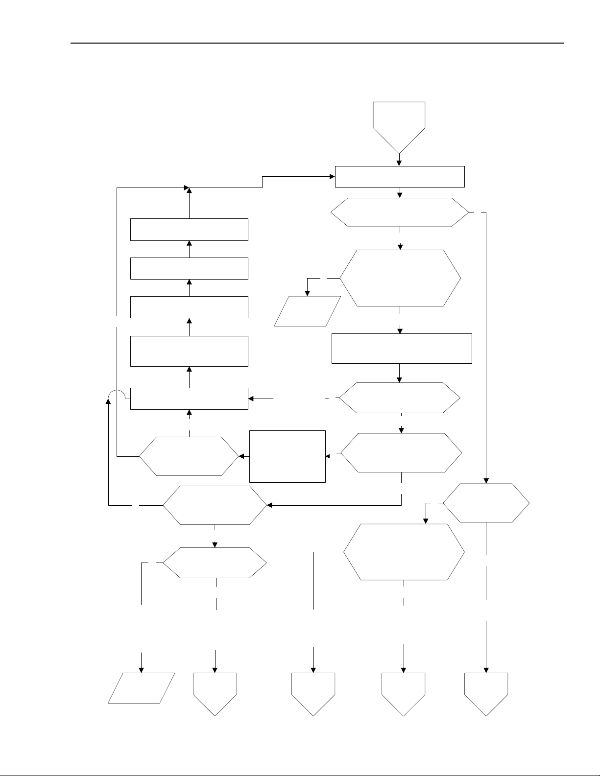
KPCI-3130 Series User’s Manual Advanced Troubleshooting B-5
Figure B-2
Problem isolation Scheme B: installation
From
Scheme A or
new install
Attempt to start the Analog I/O Panel
Reinstall KPCI-3130
Series boards
Reinstall KPCI-3130 DriverLINX
Uninstall KPCI-3130 DriverLINX
Y
Remove all KPCI-3130 Series
boards from the list of devices in
Device Manager
Remove the KPCI-3130 Series
boards from the system
N
Does the board
appear fully
installed and
configured?
Is the board listed
Y
in Device Manager
under ? Other
Devices?
Contact
Keithley
Parts of
DriverLINX
may not be
installed
correctly
Try to configure the
board from the
DriverLINX
Configuration Panel
Does Analog I/O Panel start
and display correctly?
N
Has the board and/or
Y
Y
Y
DriverLINX been re-
installed or
reconfigured?
N
Perform configuration checks in
Device Manager and DriverLINX
Configuration Panel
Does the board appear
fully installed and
configured?
N
Is the board listed in
Device Manager under
DriverLINX but not fully
configured?
N
Y
N
Is this a new
installation?
N
Problem
resolution
is beyond
scope of this
procedure
Contact
Keithley
N
Is this a new
Installation?
Y
System problems
need resolved before
installation can be
completed
Go to
Scheme A
N
Installation
configuration errors
may be eliminated as
problem cause
Go to
Scheme C
Has the board and/or
DriverLINX been re-
installed or
reconfigured?
Y
Corrected Installation/
configuration
seems to have fixed the
problem
Go to
Scheme G
Y
Installation
is OK
Return to
install

B-6 Advanced Troubleshooting KPCI-3130 Series User’s Manual
1. Attempt to start the DriverLINX Analog I/O Panel, as follows:
a. In the Start menu, click Programs.
b. Locate the DriverLINX → Test Panels folder.
c. Click AIO Panel.
2. If the DriverLINX Analog I/O Panel appears:
NOTE The exact layout of the DriverLINX Analog I/O Panel depends on the
number and kind of DriverLINX boards installed in the system.
a. Select the KPCI-3130 Series driver for the KPCI-3130 and KPCI-3132 boards from the
Driver Selection list and the appropriate device number from the Device Selection list
(0 if only one KPCI-3130 Series board is installed).
b. Verify that the Analog I/O Panel specific to the KPCI-3130 or KPCI-3132 is displayed.
NOTE If the appropriate driver is not available from the Driver Selection list,
go to Step 4.
c. Go to Step 12.
3. If the DriverLINX Analog I/O Panel does not start:
a. If this is the first time through this scheme for this specific problem, go to step 4.
b. If this is not the first time through this scheme for this specific problem (i.e., DriverLINX
and the board have be re-installed), the problem lies beyond the scope of this procedure.
Refer to the instructions provided in “Technical support” and contact Keithley for further
assistance.
4. Determine if and how the KPCI-3130 Series board is listed in the Windows Device
Manager, as follows:
a. Right-click the My Computer icon on the desktop to display its shortcut menu.
b. On the shortcut menu, click Properties. The System Properties dialog box opens.
c. In the System Properties dialog box:
• For Windows 2000, click the Hardware tab and the Device Manager ... button.
• For Windows 95/98, click the Device Manager tab.
d. In the Device Manager, with View devices by type selected, locate the DriverLINX
drivers item.
e. Click the + sign to the left of the DriverLINX drivers item. A list of all installed Driver-
LINX boards should appear.
1. If the KPCI-3130 Series board is recognized as a device under DriverLINX and is
configured to work with DriverLINX (i.e., the board is listed without a large exclamation point over it), keep the Device Manager open and go to step 5.
2. If one or more KPCI-3130 Series boards are recognized as a device under DriverLINX but are not configured to work with DriverLINX (i.e., board displayed with a
large exclamation point over it) keep the Device Manager open and go to step 5.
f. If there is a ? Other Devices listed and one or more KPCI-3130 Series boards listed
under ? Other Devices, keep the Device Manager open and go to step 5.
g. If the KPCI-3130 Series board is listed in more than one place in the Device Manager,
go to step 6.
h. If the installed KPCI-3130 Series board is not listed anywhere in the Device Manager:
1. If basic system operation has not been verified using the procedure in scheme A, go to
Scheme A.
2. If basic system operation has been verified using the procedure in Scheme A, the
problem lies beyond the scope of this procedure. Refer to the instructions provided in
“Technical support” and contact Keithley for further assistance.

KPCI-3130 Series User’s Manual Advanced Troubleshooting B-7
5. Determine whether the KPCI-3130 Series board is recognized by and properly configured
for DriverLINX, as follows:
a. In the Start menu, click Programs.
b. Locate the DriverLINX folder and click DriverLINX Configuration Panel. The
DriverLINX Configuration Panel appears.
c. If Keithley KPCI-3130 Series is listed under DriverLINX with a pale grey amplifier
icon and a device number (e.g., Device0 or Device1) is listed under it with a green lamp
icon, the board is recognized as a device under DriverLINX and is properly configured.
The inability to run the Analog I/O Panel may be due to an improperly installed component of DriverLINX. Go to step 8.
d. If Keithley KPCI-3130 Series is listed under DriverLINX with a yellow amplifier icon
and Keithley KPCI-3130 Series Analog Board is listed under it with an unlit lamp icon,
the board is recognized as a device under DriverLINX but not properly configured. Keep
the configuration panel open and go to step 6.
6. Reconfigure each unconfigured board from the DriverLINX configuration panel, as follows:
a. Click on the name of the Keithley KPCI-3130 Series Analog Board to configure.
NOTE Boards that are not properly configured are indicated by an unlit lamp
icon to the left of the board name.
b. Click the Configure button. The Select Logical Device Number dialog box appears as in
Figure B-3.
Figure B-3
Selecting the logical device number

B-8 Advanced Troubleshooting KPCI-3130 Series User’s Manual
1. If only one KPCI-3130 Series board is installed, click OK to select the displayed
default device number of 0. The Configure DriverLINX Device dialog box
(Figure B-4) appears.
2. If more than one KPCI-3130 Series boards are installed and configured and have been
assigned device numbers, enter a device number for the board being configured and
click OK. The Configure DriverLINX Device dialog box (Figure B-4) appears.
NOTE The device number entered should be the next unassigned number in the
numbering sequence.
c. Click OK to close the Configure DriverLINX Device dialog box. A Device Change
message may be displayed, as in Figure B-5.
Figure B-4
Configure DriverLINX Device dialog box example
d. Click OK to close the Device Change message box (Figure B-5).
Figure B-5
Device Change message
e. Repeat steps a through f for each KPCI-3130 Series board that needs reconfigured.
f. Close all programs and reboot the computer.
g. Open the Device Manager (as in Step 4) and verify that all installed KPCI-3130 Series
board(s) are listed under DriverLINX without exclamation marks.
h. Open and check the DriverLINX Configuration panel (as in step 5).
1. If the KPCI-3130 Series board(s) is properly configured, go back to Step 1 and retry
starting the Analog I/O Panel.

KPCI-3130 Series User’s Manual Advanced Troubleshooting B-9
NOTE Properly configured boards are indicated as device numbers with green
lamp icons.
2. If the KPCI-3130 Series board(s) is not properly configured, there may be a problem
with the DriverLINX and KPCI-3130 Series board installation. Go to step 7.
7. Physically uninstall all KPCI-3130 Series boards, as follows.
NOTE Remove all KPCI-3130 Series boards before reinstalling the KPCI-3130
Series version of DriverLINX. If a KPCI-3130 Series board is present,
physically or in the computer list of devices, driver installation may not
be error-free.
a. Turn OFF the computer.
b. Remove the chassis cover.
c. Remove all KPCI-3130 Series boards from their computer expansion slots.
d. Replace the chassis cover.
e. Restart the computer.
CAUTION Wear a grounded wrist strap to avoid electrostatic damage to the
board. Do not touch board components or conductors when handling the board.
8. Remove all KPCI-3130 Series boards from the list of devices in the Device Manager, as
follows:
NOTE KPCI-3130 Series boards may be listed under the DriverLINX drivers
item or the ? Other Devices item.
For Windows 95/98:
a. Open the Device Manager by right clicking the My Computer icon, clicking Properties
on the menu that appears, then clicking the Device Manager tab. A list of installed
devices appears.
b. Locate all KPCI-3130 Series boards in the Device Manager.
c. Select one of the KPCI-3130 Series boards.
d. At the bottom of the list of devices, click Remove. A Confirm Device Removal dialog
box appears.
e. Click OK. The board is removed from the list of devices.
f. If more than one KPCI-3130 Series board was listed in the Device Manager, repeat steps
c, d, and e until all KPCI-3130 Series boards are removed from the Device Manager.
For Windows NT:
a. Run Control Panel and double click on Devices.
b. Stop the DriverLINX for Keithley 3130 Series device driver. If the device driver does
not stop, set the startup type to disabled and reboot the computer.
c. Shut down and restart the computer.
For Windows 2000:
a. From the Add/Remove Hardware Wizard, click Next.
b. Click Uninstall/Unplug a device.
c. Click Uninstall a device.
d. Select the DriverLINX for Keithley 3130 Series.

B-10 Advanced Troubleshooting KPCI-3130 Series User’s Manual
9. Uninstall only the KPCI-3130 Series versions of DriverLINX from the system as follows:
a. In the Start menu of Windows 95/98/NT/2000, click Settings → Control Panel.
b. In the Control Panel, click Add/Remove Programs. A dialog box appears.
c. In the Add/Remove Programs Properties dialog box, select DriverLINX for Keithley
3130 Series.
NOTE Uninstall only DriverLINX for Keithley 3130 Series. If additional
DriverLINX versions are installed, leave them installed.
d. For Windows 95/98/NT, at the bottom of the Add/Remove Programs Properties dialog
box, click Add/Remove and follow the Windows uninstall prompts. For Windows 2000,
click Change/Remove and follow the Windows uninstall prompts.
CAUTION During the uninstall procedure, the system typically asks to delete
files that may be shared by other programs. Always click No. Unin-
stalling files needed by other programs may cause serious problems,
whereas leaving unneeded installed files will not harm the system.
10. Reinstall DriverLINX, using the procedure outlined in Section 3, “Installing DriverLINX.”
11. Reinstall the board(s), as follows:
CAUTION Wear a grounded wrist strap to avoid electrostatic damage to the
board. Do not touch board components or conductors when handling the board.
NOTE If Scheme B is being performed independently as an installation check,
reinstall all boards removed in step 9. If Scheme B is being performed as
part of the systematic problem isolation procedure, reinstall only the
known good board (refer to Scheme A).
a. Shut down and turn OFF the computer.
b. Install the board(s) in its expansion slot(s) using the procedure outlined in Section 3,
“Installing the KPCI-3130 Series boards.”
c. Turn ON and reboot the computer.
d. Configure the board and software using the procedure outlined in Section 3,
“Configuring the software and board.”
e. Return to step 1 and run the installation check again.
12. DriverLINX and the KPCI-3130 Series board(s) are installed correctly.
a. If starting the I/O panel was performed as an installation check, return to Section 4 and
finish installing the data acquisition system, starting with Section 4, “Identifying I/O con-
nector pin assignments for KPCI-3130 Series.”
b. If starting the I/O panel was performed as part of the systematic problem isolation proce-
dure AND the board has been reconfigured and/or DriverLINX has been re-installed, go
to “Problem isolation Scheme G: verification of problem solution.”
c. If starting the I/O panel was performed as part of the systematic problem isolation proce-
dure AND the board and DriverLINX software were not re-configured or re-installed to
allow the test panel to start, then the problem must lie elsewhere. Go to “Problem isola-
tion Scheme C: application software” to check for application software issues.

KPCI-3130 Series User’s Manual Advanced Troubleshooting B-11
Problem isolation Scheme C: application software
Scheme C:
• Checks custom application software source code.
• Checks compatibility and installation of commercial application software.
A flow chart is provided in Figure B-6.
NOTE The known good board installed in Scheme A should still be installed.
This eliminates possible board I/O problems during Scheme C.
NOTE This is not a stand-alone procedure and should only be used when called
for by another procedure.
1. Perform the procedure outlined in the “Analog output software test” found later in this
Appendix.
NOTE If the software appears not to be working properly with the analog out-
puts, go to step 4.
2. Perform the procedure outlined in the “General-purpose digital I/O software test (KPCI-
3130 only)” found later in this Appendix.
NOTE If the software appears not to be working properly with the digital I/O,
go to step 4.
3. If the software appears to be working with both the analog outputs (3130 Series) and the
digital I/O (KPCI-3130 board only), go to “Problem isolation Scheme E: user wiring” and
check the external connections.
4. If the applications program is a proven program (i.e., a commercial program that cannot be
modified), the software may be installed incorrectly or may be incompatible with DriverLINX. Contact the program manufacturer and verify that the current version of the program
is installed, that it is installed correctly, and that it is compatible with DriverLINX.
a. If the program is the current version and is installed correctly and is compatible with
DriverLINX, refer to “Technical support” and contact Keithley.
b. If the program is not the current version or is not installed correctly:
1. Correct program installation as required.
2. Repeat the “Analog output software test” and the “General-purpose digital I/O
software test (KPCI-3130 only)” found later in this Appendix.
3. If the software appears to be working, go to Scheme G to verify the problem solution.
4. If the software still does not work, refer to “Technical support” and contact Keithley.
5. If the applications program is a custom program that can be modified:
a. Check and debug the source code as necessary.
b. Repeat the “Analog output software test” and the “General-purpose digital I/O software
test (KPCI-3130 only)” found later in this Appendix.
1. If the software appears to be working, go to Scheme G to verify the problem solution.
2. If the software still does not work, refer to “Technical support” and contact Keithley.

B-12 Advanced Troubleshooting KPCI-3130 Series User’s Manual
Figure B-6
Problem isolation Scheme C: application software
From
Scheme B
Perform analog output
software test
Do the analog
N
outputs work with
the software?
Y
Perform general-purpose digital
I/O software test
Is the application program a custom
program?
Y
Is the source code available
for debugging?
Y
Has the program
been debugged?
N
Check & debug the custom application
program
Contact
Keithley
N Y
N
Y
Does the digital
I/O work with the
software?
N
Is the application
program
compatible with
DriverLINX?
N
Is the
application
program the
current
version and
installed
correctly?
Reinstall the
application program
modified or
Y
re-installed?
Fixes to
application
software seem
to have solved
the problem
Go to
Scheme G
Has the
software
been
N
Application
software is
eliminated as
the source of
the problem
Go to
Scheme E

KPCI-3130 Series User’s Manual Advanced Troubleshooting B-13
Problem isolation Scheme D: expansion slot connectors
Scheme D checks for expansion slot malfunctions.
Refer to the flow chart in Figure B-7.
NOTE This is not a stand-alone procedure. Use it only when it is called for by
another procedure.
1. Shut down Windows 95/98/NT/2000 and turn OFF power to the host computer.
2. Remove the known good KPCI-3130 Series board from the suspect PCI slot.
3. Determine what PCI devices are recognized by the system, as follows:
a. Insert a blank diskette, or any unbootable diskette, into the A: drive.
b. Turn ON the computer and allow it to start the boot cycle.
c. When the boot cycle stalls, note and record the displayed PCI device listing… (If a
printer is attached to the system, press the PRINT SCREEN key to print a copy of the
screen.)
d. Remove the diskette, press any key, and allow the boot cycle to finish.
4. Shut down Windows 95/98/NT/2000 and turn OFF power to the host computer.
5. Securely reseat the known good board in the suspect slot.
6. Determine if the system recognizes the board as a new PCI device in the suspect slot, as
follows:
a. Insert a blank diskette, or any unbootable diskette, into the A: drive.
b. Turn ON the computer and allow it to start the boot cycle.
c. When the boot cycle stalls, note and record the displayed PCI device listing… (If a
printer is attached to the system, press the PRINT SCREEN key to print a copy of the
screen.)
d. Compare the PCI device listing to that recorded in Step 3.
e. Remove the diskette, press any key, and allow the boot cycle to finish.
7. If the board is found as a new PCI device, replace the known good board with the suspect
board removed in Scheme A and go to Scheme G to verify the solution.
8. If the board is not recognized as a new PCI device and there is another available PCI slot:
a. Shut down Windows 95/98/NT/2000 and turn OFF power to the host computer.
b. Remove the KPCI-3130 Series board from the system.
c. Determine what PCI devices are recognized by the system as in Step 3.
d. Securely seat the known good board in a free PCI slot.
e. Determine if the system recognizes the board as a new PCI device in the appropriate slot,
as in Step 6.
1. If the board is found as a new PCI device, replace the known good board with the suspect board removed in Scheme A and go to Scheme G to verify the solution.
2. If the board is not recognized as a new PCI device, refer to “Technical support” and
contact Keithley for further assistance.

B-14 Advanced Troubleshooting KPCI-3130 Series User’s Manual
Figure B-7
Problem isolation Scheme D: expansion slot connectors
From
Scheme A
properly seated
Replace the known
good board with the
suspect board removed
in Scheme A
Go to
Scheme G
Board was not
Board is now
functional PCI
seated in a
slot
Remove the known good KPCI-3130 Series board
Determine what PCI devices are recognized by the system
Securely reseat the known good board in a suspect slot
Y
Y
Does the system recognize the board as a PCI device?
Is there another available PCI slot? N
Remove the known good KPCI-3130 Series board
Determine what PCI devices are recognized by the system
Securely reseat the known good board in a free slot
Does the system recognize the board as a PCI device?
from the system
N
Y
from the system
N
Service/Replace
the PCI slot
Contact
Keithley
9. If the board is not recognized as a new PCI device and there is not another available PCI slot:
a. Shut down Windows 95/98/NT/2000 and turn OFF power to the host computer.
b. Remove the KPCI-3130 Series board from the system.
c. Service or replace the PCI slot.
d. Securely seat the board in the serviced slot.
e. Determine if the system recognizes the board as a new PCI device in the serviced slot, as
in Step 6.
1. If the board is found as a new PCI device, replace the known good board with the suspect board removed in Scheme A and go to Scheme G to verify the solution.
2. If the board is not recognized as a new PCI device, refer to “Technical support” and
contact Keithley for further assistance.

KPCI-3130 Series User’s Manual Advanced Troubleshooting B-15
Problem isolation Scheme E: user wiring
Scheme E checks external connections.
Refer to the flow chart in Figure B-8.
NOTE This is not a stand-alone procedure. Use it only when it is called for by
another procedure.
Figure B-8
Problem isolation Scheme E: user wiring
From
Scheme C
Check external user connections for short
N
Resolve
external user
connections
Go to
Scheme G
and open circuits
External user
connection ok?
User connections are not the
Y
cause of the problem
Go to
Scheme F
1. Check the I/O connections between each external signal source and the screw terminal
accessory, one at a time, for short circuits and open circuits. If KPCI-3130 Series boards
were installed in more than one PCI slot, check the I/O connections for all boards.
NOTE Do not connect the screw terminal accessory to the board during this
scheme.
2. If any external I/O connections are found to be faulty:
a. Correct the faulty external connections.
b. Go to “Problem isolation Scheme G: verification of problem solution.”
3. If all external I/O connections are found to be normal, the KPCI-3130 Series board(s) originally installed in the computer may be the cause of the problem:
a. If there is only one KPCI-3130 Series board installed in the system or suspected to be
faulty:
1. Replace the faulty board with a known good board.
2. Go to “Problem isolation Scheme G: verification of problem solution.”
b. If there is more than one KPCI-3130 Series board installed in the system, go to Scheme F
to determine which board is faulty.

B-16 Advanced Troubleshooting KPCI-3130 Series User’s Manual
Problem isolation Scheme F: the board
Scheme F determines which KPCI-3130 Series board is faulty (assuming more than one board is
installed in the system).
Refer to Figure B-9 for a flow chart.
NOTE This is not a stand-alone procedure. Use it only when it is called for by
another procedure.
Figure B-9
Problem isolation Scheme F: the board
From
Scheme E
Remove all suspect KPCI-3130
Series boards from the system
Select a suspect KPCI-3130
Series board to test
Determine what PCI devices are
recognized by the system
Replace the
faulty board(s)
Install the board being tested in a
known good PCI slot
Determine and note if the board is
recognized as a PCI device
Have all suspect boards been tested?
Y
Were all boards
N
N
KPCI-3130 board only
N
recognized as a PCI
device?
Select a suspect board
Perform Analog output hardware
test on the board
Does the board pass
the test?
Y
Perform General-purpose digital
I/O hardware test
Y
Does the board pass
Y
the test?
Y
N
Go to
Scheme G
Have all suspect boards
been tested?
Y
Contact
Keithley
N

KPCI-3130 Series User’s Manual Advanced Troubleshooting B-17
1. Shut down Windows 95/98/NT/2000 and turn OFF power to the host computer.
2. Remove all KPCI-3130 Series boards from the system.
3. Determine what PCI resources are already recognized by the system, as follows:
a. Insert a blank diskette, or any unbootable diskette, into the A: drive.
b. Turn ON the computer and allow it to start the boot cycle.
c. When the boot cycle stalls, note and record the displayed PCI device listing… (If a
printer is attached to the system, press the PRINT SCREEN key to print a copy of the
screen.)
d. Remove the diskette, press any key, and allow the boot cycle to finish.
4. Again, shut down Windows 95/98/NT/2000 and turn OFF power to the host computer.
5. Install, in any available known good PCI slot, one of the suspected KPCI-3130 Series
boards.
6. Determine if the system recognizes the board as a new PCI device, as follows:
a. Insert a blank diskette, or any unbootable diskette, into the A: drive.
b. Turn ON the computer and allow it to start the boot cycle.
c. When the boot cycle stalls, note and record the displayed PCI device listing… (If a
printer is attached to the system, press the PRINT SCREEN key to print a copy of the
screen.)
d. Remove the diskette, press any key, and allow the boot cycle to finish.
e. Compare the PCI device listing to that recorded in step 3c.
7. Repeat steps 1 through 6 for each KPCI-3130 Series board in the system, noting which
boards are recognized as PCI devices.
8. If any of the boards tested were not recognized as PCI devices:
a. Replace the faulty board with a known good board.
b. Go to “Problem isolation Scheme G: verification of problem solution.”
9. If all of the boards tested were recognized as PCI devices:
a. Perform the procedure outlined in the “Analog output hardware test” found later in this
Appendix for each board, noting which boards pass the test.
b. Perform the procedure outlined in the “General-purpose digital I/O hardware test
(KPCI-3130 only)” found later in this Appendix, noting which boards pass the test.
10. If any of the boards failed either the Analog output hardware test or the General-purpose
digital I/O hardware test (KPCI-3130 only):
a. Replace the faulty board(s) with a known good board.
b. Go to “Problem isolation Scheme G: verification of problem solution.”
11. If all of the boards passed the Analog output hardware test and the General-purpose digital
I/O hardware test (KPCI-3130 only), refer to “Technical support” and contact Keithley for
further assistance.

B-18 Advanced Troubleshooting KPCI-3130 Series User’s Manual
Problem isolation Scheme G: verification of problem solution
Scheme G verifies that the system problem has been resolved. Refer to Figure B-10 for a flow
chart of the procedure.
NOTE This is not a stand-alone procedure. Use it only when it is called for by
another procedure.
Figure B-10
Problem isolation Scheme G: verification of problem solution
From
Scheme
A,B,C,D,E,
or F
Install all required KPCI-3130 Series boards
Contact
Keithley
in the appropriate slots
Reconnect all external circuits
Start the system and the data
acquisition software
Repeat task(s) being performed when
problems occurred
Is the system operating properly?N
Y
Congratulations!
The problem seems resolved.
1. Shut down Windows and turn OFF power to the computer.
2. Install the required KPCI-3130 Series boards in appropriate slots.
3. Reconnect all external circuits.
NOTE If external circuits were left connected to the screw terminal accessory,
connect the accessory to the board. If the external circuits were disconnected from the screw terminal accessory, reconnect them and the accessory as discussed in Section 3, “Installation.”
4. Turn ON the computer and start the data acquisition software.
5. Repeat the task(s) being performed when problems occurred.
6. Observe system performance.
7. If the system is operating properly, congratulations on resolving the problem.
8. If the system is not operating properly, refer to “Technical support” and contact Keithley for
further instructions.

KPCI-3130 Series User’s Manual Advanced Troubleshooting B-19
Specified hardware I/O tests
The tests in this section check performance of the KPCI-3130 Series board’s analog and also the
KPCI-3130’s digital I/O.
The tests use proven DriverLINX utilities, thereby bypassing any unresolved application software issues.
These tests are intended to be used when specified in the preceding “Systematic problem isola-
tion” procedure. However, they may also be used at any time for general functional checks of the
KPCI-3130 Series board.
NOTE During these tests, disconnect all user circuits from the board, except as
specified in individual test procedures.
Analog output hardware test
The analog output test checks whether the digital-to-analog converters (DACs) of the board are
working correctly. Zero voltages are set at the analog outputs, using the on-screen level control
utility supplied with DriverLINX. The two output voltages are then measured with a digital voltmeter to verify reasonable DAC offsets. Similarly, a mid-range voltage is set for each of the analog outputs and the procedure is repeated to verify proper digital to analog conversion.
NOTE During this test, ensure that no user circuits are connected to the
KPCI-3130 Series board, via the required screw terminal accessory,
except for analog output connections specified for the test.
The analog output test is primarily a functional test, not a calibration
check, although measured outputs from a properly calibrated board
should correspond to DAC settings, within the accuracy specifications of
the board. To check and adjust accuracy, refer to Section 5,
“Calibration.”
Equipment
The following equipment is required to perform the analog output test:
• A Digital Voltmeter (DVM) or a Digital Multimeter (DMM) set to the 10V range.
• An STP-36 screw terminal accessory, to which the DVM/DMM is connected as indicated
in Table B-1.
NOTE If possible, use a screw terminal accessory that is reserved for I/O tests.
Using the screw terminal accessory normally connected to the external
circuits may lead to potential wiring errors involved in disconnecting
and later reconnecting the external circuits.

B-20 Advanced Troubleshooting KPCI-3130 Series User’s Manual
Table B-1
Terminals on accessory for connection during analog output hardware test
To check this
analog output
(local sense)…
Analog output 0 1, 2 shorted 19, 20 shorted
Analog output 1 3, 4 shorted 21, 22 shorted
Analog output 2 5, 6 shorted 23, 24 shorted
Analog output 3 7, 8 shorted 25, 26 shorted
Analog output 4 9, 10 shorted 27, 28 shorted
Analog output 5 11, 12 shorted 29, 30 shorted
Analog output 6 13, 14 shorted 31, 32 shorted
Analog output 7 15, 16 shorted 33, 34 shorted
…connect the DVM or DMM to these terminals:
Analog output and sense
high screw terminals
Analog ground and sense
low screw terminals
Models
KPCI-3130 and
KPCI-3132
KPCI-3130
only
Procedure
1. Turn OFF the host computer.
2. Connect the negative lead of the DVM/DMM to a ground terminal and sense low of the
screw terminal accessory, as indicated in Table B-1.
3. Connect the STP-36 screw terminal accessory to the KPCI-3130 Series “Analog” I/O
connector.
4. Turn ON the host computer and boot Windows 95/98/NT/2000.
5. In the Start menu, click Programs.
6. Locate the DriverLINX → Test Panels folder and click on AIO Panel. A setup screen is
displayed (see Figure B-11).
Figure B-11
Analog I/O Panel setup screen example
KPCI3130

KPCI-3130 Series User’s Manual Advanced Troubleshooting B-21
NOTE Refer to Section 4, “Making two-wire and four-wire mode connections”
for making accurate analog output measurements.
7. Click the Level Control tab. The on-screen analog-output level control appears, similar to
Figure B-12.
Figure B-12
On-screen analog-output level control
8. Enable CH0 by clicking on the rectangular button below the channel voltage reading.
9. Using the mouse, slide the CH0 level control button until the tiny display at the bottom of the
level control reads 0.0 (volts).
10. Repeat Steps 8 and 9 for each analog channel.
11. Measure and compare the analog output voltages as indicated in Table B-2:
a. Measure the voltages with the DVM/DMM at the applicable analog outputs.
• KPCI-3130 → Analog outputs 0 and 7
• KPCI-3132 → Analog outputs 0 and 1
b. Compare the voltages measured in step 11a with the voltages set via the analog-output
level control.
12. Verify overload detection on a specific channel, as follows:
a. Perform a disconnect on a two-wire or four-wire setup at the channel.
b. Open the AIO Test Panel.
c. Click on the DIO tab.
d. On the Input Panel, select Channel 4.
e. Verify a zero in the applicable bit (bit 7 represents channel 7, bit 6 represents channel 6,
etc.).

B-22 Advanced Troubleshooting KPCI-3130 Series User’s Manual
Table B-2
Test connections and readings for zero-voltage analog output connected to upper “Analog” I/O connector
…connect the DVM or DMM to these
terminals on an STP-36 accessory:
To check this
analog output
(local sense)…
Analog output 0 1, 2 shorted 19, 20 shorted 0.0V 0.0V
Analog output 1 3, 4 shorted 21, 22 shorted 0.0V 0.0V
Analog output 2 5, 6 shorted 23, 24 shorted 0.0V 0.0V
Analog output 3 7, 8 shorted 25, 26 shorted 0.0V 0.0V
Analog output 4 9, 10 shorted 27, 28 shorted 0.0V 0.0V
Analog output 5 11, 12 shorted 29, 30 shorted 0.0V 0.0V
Analog output 6 13, 14 shorted 31, 32 shorted 0.0V 0.0V
Analog output 7 15, 16 shorted 33, 34 shorted 0.0V 0.0V
Analog output
and sense high
screw terminals
13. Enable CH0 by clicking on the rectangular button below the channel voltage reading.
14. Using the mouse, slide the CH0 level control button until the tiny display at the bottom of the
level controls read 5.0.
15. Repeat Steps 12 and 14 for each analog output channel.
16. Measure and compare the analog output voltages as indicated in Table B-3:
a. Measure the voltages at analog outputs with the DVM/DMM.
b. Compare the voltages measured in step 15a with the voltages set via the analog-output
level control.
Analog ground
and sense low
screw terminals
If the board works correctly, the
following voltages should agree:
Voltage
Level control
setting
reading at
DVM or DMM
Models
KPCI-3130 and
KPCI-3132
KPCI-3130 only
Table B-3
Test connections and readings for mid-range analog output connected to upper “Analog” I/O connector
…connect the DVM or DMM to these
terminals on an STP-36 accessory:
To check this
analog output
(local sense)…
Analog output 0 1, 2 shorted 19, 20 shorted 5.0V 5.0V
Analog output 1 3, 4 shorted 21, 22 shorted 5.0V 5.0V
Analog output 2 5, 6 shorted 23, 24 shorted 5.0V 5.0V
Analog output 3 7, 8 shorted 25, 26 shorted 5.0V 5.0V
Analog output 4 9, 10 shorted 27, 28 shorted 5.0V 5.0V
Analog output 5 11, 12 shorted 29, 30 shorted 5.0V 5.0V
Analog output 6 13, 14 shorted 31, 32 shorted 5.0V 5.0V
Analog output 7 15, 16 shorted 33, 34 shorted 5.0V 5.0V
Analog output
and sense high
screw terminals
17. Determine whether the board passed or failed the analog output hardware test, as follows:
• If the voltages measured with the DVM/DMM do not agree with the level control set-
tings, the board failed the analog output hardware test.
• If the voltages measured with the DVM/DMM do agree with the level control settings,
the board passed the analog output hardware test.
18. Return to step 10 in “Problem isolation Scheme F: the board.”
Analog ground
and sense low
screw terminals
If the board works correctly, the
following voltages should agree:
Voltage
Level control
setting
reading at
DVM or DMM
KPCI-3130 and
KPCI-3132
KPCI-3130 only
Models

KPCI-3130 Series User’s Manual Advanced Troubleshooting B-23
NOTE If the analog outputs appear to work satisfactorily, but some measured
analog output voltages are outside the accuracy limits specified in
Appendix A, consider calibrating the board after concluding the
“Systematic problem isolation” procedure. For calibration procedures,
refer to Section 5, “Calibration.”
General-purpose digital I/O hardware test (KPCI-3130 only)
This test checks whether the general-purpose digital input and output circuits of the board are
operating properly.
Test summary
• Wire an STP-36 screw terminal accessory in a loop-back configuration. Connect the channel
0 digital I/O terminals, bit-for-bit, to the channel 2 digital I/O terminals. Connect the channel
1 terminals, bit-for-bit, to the channel 3 terminals. See Figure B-13 for the channel and bit
number of each terminal on the screw terminal accessory. See Figure B-14 for the loop-back
wiring schematic. (These are the same connections as made for the general-purpose digital
I/O software test.)
Figure B-13
Channel and bit numbers for an STP-36 screw terminal accessory (KPCI-3130 only)
Channel 2
Channel 3
Bit 16
Bit 17
Bit 18
Bit 19
Bit 20
Bit 21
Bit 22
Bit 23
Bit 24
Bit 25
Bit 26
Bit 27
Bit 28
Bit 29
Bit 30
Bit 31
+5V
+5V
19
2021
2223
24
25
26
27
28
2930
31
3233
34
3536
Bit 0
Bit 1
Bit 2
Bit 3
Bit 4
Bit 5
Bit 6
Bit 7
Bit 8
Bit 9
1012131415161718 11 123546789
Bit 10
Bit 11
Bit 12
Bit 13
Bit 14
Bit 15
Digital Ground
Digital Ground
Channel 0
Channel 1

B-24 Advanced Troubleshooting KPCI-3130 Series User’s Manual
Figure B-14
Loop-back wiring for general-purpose digital I/O hardware and software test
(KPCI-3130 only)
R
R
R
R
R
R
R
R
12354678
19
2021
2223
24
25
26
27
28
2930
31
3233
34
3536
R
R
R
R
1012131415161718 11 9
R
R
R
R
R = 600Ω to 1000Ω

KPCI-3130 Series User’s Manual Advanced Troubleshooting B-25
• Using a DriverLINX graphical interface, configure the channel 0 and 1 bits as outputs and
the channel 2 and 3 bits as inputs.
• Using the same DriverLINX graphical interface, set the channel 0 and 1 outputs in a particu-
lar bit pattern and check channels 2 and 3 inputs for the same bit pattern. Repeat, using a second bit pattern.
The digital I/O of the board is performing satisfactorily if all bits respond appropriately. The
specified bit patterns check both for direct ON/OFF response and for shorts between bits.
Equipment
All I/O is set and read using the DriverLINX Digital Input/Output test panel; no instruments are
required. However, an STP-36 screw terminal accessory must be wired in the loop-back configuration shown in Figure B-14.
NOTE If possible, use a screw terminal accessory that is reserved for I/O tests.
Using the screw terminal accessory normally connected to the external
circuits may lead to potential wiring errors involved in disconnecting
and later reconnecting the external circuit.
Procedure
1. Turn OFF the host computer.
2. If a screw terminal accessory is attached to the upper “Analog” I/O connector of the
KPCI-3130 I/O board, remove it. No circuits should be connected to the “Analog” I/O connector during these tests.
3. Wire an STP-36 screw terminal accessory as described in Figure B-14.
4. Attach the wired screw terminal accessory to the lower “Digital” I/O connector of the
KPCI-3130 board. Refer to Section 4, “Connecting interface accessories.”
5. Turn ON the host computer and boot Windows 95/98/NT/2000.
6. In the Start menu, click Programs.
7. Locate the DriverLINX → Test Panels folder.
8. Click on the AIO Panel entry. The Analog I/O Panel setup screen appears.
9. Click the DIO tab. An on-screen digital I/O controller appears, similar to Figure B-15.
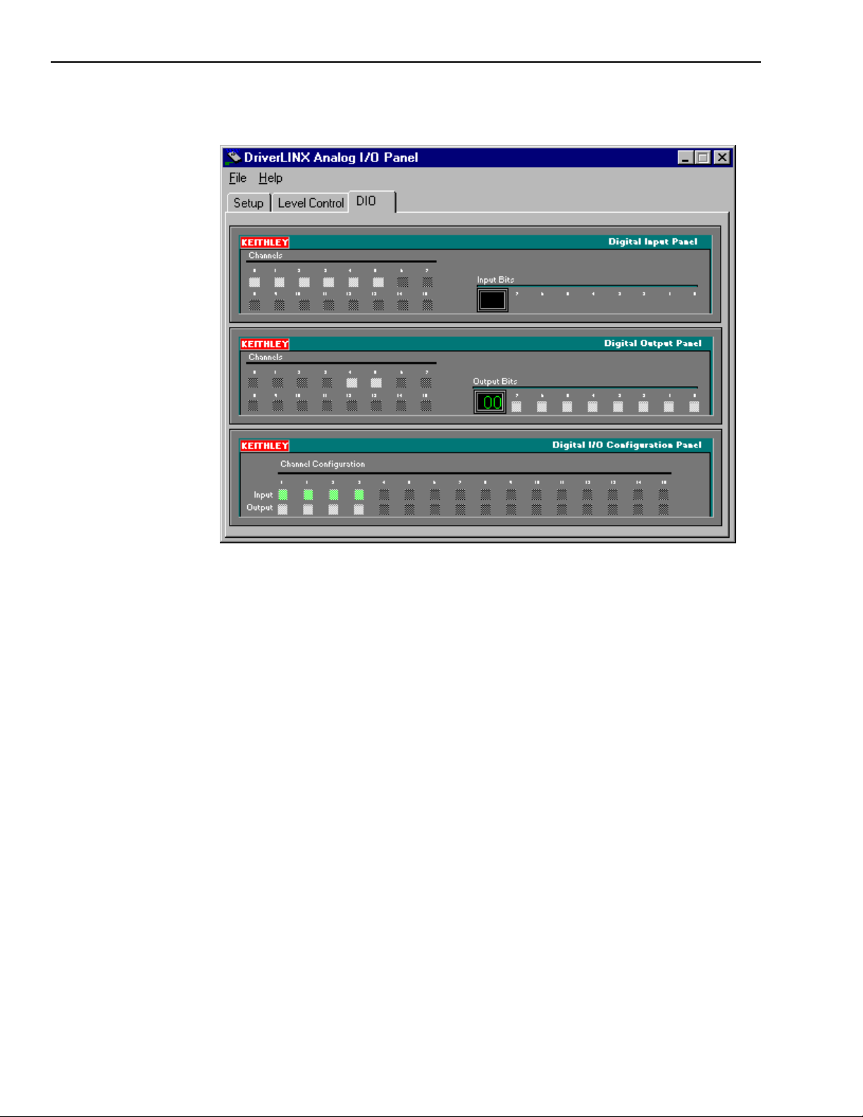
B-26 Advanced Troubleshooting KPCI-3130 Series User’s Manual
Figure B-15
On-screen digital I/O controller

KPCI-3130 Series User’s Manual Advanced Troubleshooting B-27
NOTE The on-screen digital I/O controller works as follows:
• Channel 0 refers to the twelve multi-function digital I/O bits. These
bits may be manipulated with the digital I/O controller only when the
multi-function bits are configured as general-purpose bits.
• Channels 1 to 4 refer to the four 8-bit general-purpose registers in
the KPCI-3130. Bits displayed on the Digital Input Panel and the
Digital Output Panel are numbered 0-7 for every channel—instead
of 0-7 for channel 0, 8-15 for channel 1, 16-23 for channel 2, and
24-31 for channel 3 as for the KPCI-3130 “Digital” I/O connector.
Refer to Table B-4.
• Invalid channels and settings appear as dark gray squares. For
example:
– Non-existent channels always appear as dark gray squares.
– In the Digital I/O Configuration Panel, Channel 0, corresponding to the
twelve multi-function digital I/O bits, appears as dark gray squares. The
configuration of the twelve bits is fixed; six are always inputs and six are
always outputs.
• Valid channels and settings appear as white squares when OFF and
green squares when ON. (When the manual is printed in black and
white, valid channels and settings appear as white squares when
OFF and as light gray squares when ON).
• The two-digit numeric displays under Input Bits and Output Bits
show the hexadecimal values of the adjacent bit patterns.
• To configure a valid channel either for input or output, use the
Digital Channel Configuration Panel. Click on either the Input or
Output square below the channel number.
• To turn ON output-channel bits, use the Digital Output Panel. First
select the channel number of the bits to be turned ON by clicking on
the appropriate square under Channels. Then, turn ON a bit by
clicking the appropriate square under Output Bits. Turn OFF a bit
in the same way.
• To read an input-channel bit, use the Digital Input Panel. First
select the channel number to be checked by clicking the appropriate
square under Channels. Then, read the numbered bit under Input
Bits. OFF input bits appear as black dots and ON input bits appear
as green dots. (When the manual is printed in black and white, OFF
input bits appear as black dots and ON input bits appear as light
gray dots.)

B-28 Advanced Troubleshooting KPCI-3130 Series User’s Manual
Table B-4
Bit numbering on Digital I/O panel vs. “Digital” I/O connector (KPCI-3130 only)
Channel 0 bit numbers Channel 1 bit numbers Channel 2 bit numbers Channel 3 bit numbers
On I/O
panels
0 0 0 08 0 16 0 24
1 1 1 09 1 17 1 25
2 2 2 10 2 18 2 26
3 3 3 11 3 19 3 27
4 4 4 12 4 20 4 28
5 5 5 13 5 21 5 29
6 6 6 14 6 22 6 30
7 7 7 15 7 23 7 31
At “Digital”
connector
10. Under Digital I/O Configuration Panel, configure channels 0 and 1 as outputs.
11. In the Digital Output Panel under Channels, click on channel 1.
12. In the Digital Output Panel under Output Bits, set the bits of channel 1 for a bit pattern of
13. In the Digital Input Panel under Channels, click on channel 1.
14. In the Digital Input Panel under Input bits, observe the bit pattern. The proper response
15. In the Digital Output Panel under Channels, click on channel 0.
16. In the Digital Output Panel under Output Bits, configure channel 0 for a bit pattern of
17. In the Digital Input Panel under Channels, click on channel 0.
18. In the Digital Input Panel under Input bits, observe the bit pattern. The proper response
19. In the Digital Output Panel under Channels, click on channel 1.
20. In the Digital Output Panel under Output Bits, set the bits of channel 1 for a bit pattern of
21. In the Digital Input Panel under Channels, click on channel 1.
22. In the Digital Input Panel under Input bits, observe the bit pattern. The proper response
23. In the Digital Output Panel under Channels, click on channel 0.
24. In the Digital Output Panel under Output Bits, set the bits of channel 0 for a bit pattern of
On I/O
panels
0X55.
should be 0X55.
• If the displayed response is not 0X55, the digital I/O is not functioning properly. Stop
here, and return to the problem isolation step in “Problem isolation Scheme F: the board”
that asked you to perform the General-purpose digital I/O hardware test.
• If the displayed response is 0X55, continue with step 15.
0X55.
should be 0X55.
• If the observed response is not 0X55, the digital I/O is not functioning properly. Stop
here, and return to the problem isolation step in “Problem isolation Scheme F: the board”
that asked you to perform the General-purpose digital I/O hardware test.
• If the observed response is 0X55, continue with step 19.
0XAA.
should be 0XAA.
• If the observed response is not 0XAA, the digital I/O is not functioning properly. Stop
here, and return to the problem isolation step in “Problem isolation Scheme F: the board”
that asked you to perform the General-purpose digital I/O hardware test.
• If the observed response is 0XAA, continue with step 23.
0XAA.
At “Digital”
connector
On I/O
panels
At “Digital”
connector
On I/O
panels
At “Digital”
connector

KPCI-3130 Series User’s Manual Advanced Troubleshooting B-29
25. In the Digital Input Panel under Channels, click on channel 0.
26. In the Digital Input Panel under Input bits, observe the bit pattern. The proper response
should be 0XAA.
• If the observed response is not 0XAA, the digital I/O is not functioning properly.
• If the observed response is 0XAA, the digital I/O is functioning properly.
27. Stop here, and return to the problem isolation step in “Problem isolation Scheme F: the
board” that asked you to perform the General-purpose digital I/O hardware test.
NOTE When the multi-function bits are configured as general-purpose bits, a
similar test of the twelve multi-function digital I/O bits can be performed
with the on-screen digital I/O controller. Wire loop-back connections at
an STP-36 accessory between same-numbered input and output bits. (If
the outputs are always wired only to inputs, no protective series resistors
are required. If two output bits are wired together and both are turned
ON without adequate current limiting, damage will result.) Turn input
bits 0, 2, and 4 ON and look for an identical output bit pattern. Repeat,
turning input bits 1, 3, and 5 ON.
Specified software I/O tests
The tests in this section check whether the application software correctly performs analog and
digital I/O tasks. The I/O are tested using a KPCI-3130 Series board known to work properly,
thereby bypassing potential board problems. These tests are intended to be used when specified
in the preceding “Systematic problem isolation” procedure.
NOTE During these tests, disconnect all user circuits from the board, except for
connections specified in individual test procedures.
Analog output software test
This basic analog output test checks whether the application software correctly sets direct current (DC) analog output voltages. Zero volts is set at the analog outputs, using the application
software. The output voltages are then measured with a digital voltmeter to verify reasonable
DAC offsets. Similarly, a mid-range voltage is set for each of the analog outputs and the procedure is repeated.
NOTE During this test, ensure that no user circuits are connected to the
KPCI-3130 Series board, via the required screw terminal accessory,
except for analog output connections specified for the test.
The analog output software test is a software function test, not a
calibration check. To check and adjust the accuracy, refer to Section 5,
“Calibration.”
The analog output software test is only a basic check of the application
software.

B-30 Advanced Troubleshooting KPCI-3130 Series User’s Manual
Equipment
The following equipment is required to perform the analog output test:
• A Digital Voltmeter (DVM) or a Digital Multimeter (DMM) set to the 10V range.
• An STP-36 screw terminal accessory, to which the DVM/DMM is connected as indicated in
Table B-5.
NOTE If possible, use a screw terminal accessory that is reserved for I/O tests.
Using the screw terminal accessory normally connected to the external
circuits may lead to potential wiring errors involved in disconnecting
and later reconnecting the external circuit.
Table B-5
Connection terminals for analog output software test
To check this
analog output
(local sense)…
Analog output 0 1, 2 shorted 19, 20 shorted
Analog output 1 3, 4 shorted 21, 22 shorted
Analog output 2 5, 6 shorted 23, 24 shorted
Analog output 3 7, 8 shorted 25, 26 shorted
Analog output 4 9, 10 shorted 27, 28 shorted
Analog output 5 11, 12 shorted 29, 30 shorted
Analog output 6 13, 14 shorted 31, 32 shorted
Analog output 7 15, 16 shorted 33, 34 shorted
CAUTION Before powering the computer, connect the DVM/DMM negative
lead to a ground and sense-low screw terminal.
After powering the computer, connect the DVM/DMM positive lead
to each specified analog output and sense high screw terminal by
touching the tip of the lead to the screw head of the screw terminal
(for example, via a probe).
…connect the DVM or DMM to these terminals:
Analog output and sense
high screw terminals
Analog ground and sense
low screw terminals
KPCI-3130 and
KPCI-3132
KPCI-3130
Procedure for the analog output software test
Models
only
1. Turn OFF the host computer.
2. Connect the negative lead of the DVM/DMM to a ground terminal of the screw terminal
accessory, as indicated in Table B-5.
3. Connect the STP-36 screw terminal accessory to the KPCI-3130 Series I/O connector.
4. Turn ON the host computer and boot Windows 95/98/NT/2000.
5. Start DriverLINX and the application software.
6. Set the application software to output 0V at all analog outputs (0 through 7 for KPCI-3130 or
0 through 1 for KPCI-3132).
7. Measure and compare the analog output voltages as indicated in Table B-6:
a. Measure the voltages at analog outputs 0 and 1 with the DVM/DMM.
b. Compare the voltages measured in step 7a with the voltages set via the analog-output
level control.

KPCI-3130 Series User’s Manual Advanced Troubleshooting B-31
Table B-6
Test connections and readings for zero-voltage analog output
…connect the DVM or DMM to these
terminals on an STP-36 accessory:
To check this
analog output
(local sense)…
Analog output 0 1, 2 shorted 19, 20 shorted 0.0V 0.0V
Analog output 1 3, 4 shorted 21, 22 shorted 0.0V 0.0V
Analog output 2 5, 6 shorted 23, 24 shorted 0.0V 0.0V
Analog output 3 7, 8 shorted 25, 26 shorted 0.0V 0.0V
Analog output 4 9, 10 shorted 27, 28 shorted 0.0V 0.0V
Analog output 5 11, 12 shorted 29, 30 shorted 0.0V 0.0V
Analog output 6 13, 14 shorted 31, 32 shorted 0.0V 0.0V
Analog output 7 15, 16 shorted 33, 34 shorted 0.0V 0.0V
Table B-7
Test connections and readings for mid-range analog output
Analog output and
sense high screw
terminals
8. Set the application software to output +5V at analog outputs 0 and 1.
9. Measure and compare the analog output voltages as indicated in Table B-7:
a. Measure the voltages at analog outputs 0 and 1 with the DVM/DMM.
b. Compare the voltages measured in step 9a with the voltages set via the analog-output
level control.
Analog ground and
sense low screw
terminals
If the board works correctly, the
following voltages should agree:
Voltage
Level control
setting
reading at
DVM or DMM
Models
KPCI-3130 and
KPCI-3132
KPCI-3130
only
…connect the DVM or DMM to these
terminals on an STP-36 accessory:
To check this
analog output
(local sense)…
Analog output 0 1, 2 shorted 19, 20 shorted 5.0V 5.0V
Analog output 1 3, 4 shorted 21, 22 shorted 5.0V 5.0V
Analog output 2 5, 6 shorted 23, 24 shorted 5.0V 5.0V
Analog output 3 7, 8 shorted 25, 26 shorted 5.0V 5.0V
Analog output 4 9, 10 shorted 27, 28 shorted 5.0V 5.0V
Analog output 5 11, 12 shorted 29, 30 shorted 5.0V 5.0V
Analog output 6 13, 14 shorted 31, 32 shorted 5.0V 5.0V
Analog output 7 15, 16 shorted 33, 34 shorted 5.0V 5.0V
Analog output
and sense high
screw terminals
10. Determine if the application software is working correctly with the analog output portion of
DriverLINX, as follows:
• If the voltages measured with the DVM/DMM do not agree with the application software
settings, the application software is not working correctly with the analog output portion
of DriverLINX.
• If the voltages measured with the DVM/DMM agree with the application software
settings, then the software is working correctly with the analog output portion of
DriverLINX.
Analog ground
and sense low
screw terminals
If the board works correctly, the
following voltages should agree:
Output voltage
setting
Voltage reading at
DVM or DMM
Models
KPCI-3130 and
KPCI-3132
KPCI-3130
only

B-32 Advanced Troubleshooting KPCI-3130 Series User’s Manual
General-purpose digital I/O software test (KPCI-3130 only)
This test checks whether the application software is working correctly with the general-purpose
digital I/O functions of DriverLINX.
Test summary
This test includes the following steps:
• Wire an STP-36 screw terminal accessory in a loop-back configuration.
• Connect the channel 0 general-purpose digital I/O terminals, bit-for-bit, to the channel 2
general-purpose digital I/O terminals.
• Connect the channel 1 terminals, bit-for-bit, to the channel 3 terminals.
NOTE See Figure B-16 for the channel and bit number of each terminal on the
screw terminal accessory. See Figure B-17 for the loop-back wiring
schematic. (These are the same loop-back connections as made for the
general-purpose digital I/O hardware test.)
Figure B-16
Channel and bit numbers for an STP-36 screw terminal accessory (KPCI-3130 only)
Channel 2
Channel 3
Bit 16
Bit 17
Bit 18
Bit 19
Bit 20
Bit 21
Bit 22
Bit 23
Bit 24
Bit 25
Bit 26
Bit 27
Bit 28
Bit 29
Bit 30
Bit 31
+5V
+5V
19
2021
2223
24
25
26
27
28
2930
31
3233
34
3536
Bit 0
Bit 1
Bit 2
Bit 3
Bit 4
Bit 5
Bit 6
Bit 7
Bit 8
Bit 9
1012131415161718 11 123546789
Bit 10
Bit 11
Bit 12
Bit 13
Bit 14
Bit 15
Digital Ground
Digital Ground
Channel 0
Channel 1

KPCI-3130 Series User’s Manual Advanced Troubleshooting B-33
Figure B-17
Loop-back wiring for general-purpose digital I/O hardware and software test
(KPCI-3130 only)
R
R
R
R
R
R
R
R
12354678
19
2021
2223
24
25
26
27
28
2930
31
3233
34
3536
R
R
R
R
1012131415161718 11 9
R
R
R
R
R = 600Ω to 1000Ω

B-34 Advanced Troubleshooting KPCI-3130 Series User’s Manual
• Using the application software, configure the channel 0 and 1 bits as outputs and the channel
2 and 3 bits as inputs.
• Using the application software, set the channel 0 and 1 outputs in a particular bit pattern and
check channels 2 and 3 inputs for the same bit pattern. Repeat, using a second bit pattern.
The application software is performing general-purpose digital I/O satisfactorily if all bits
respond appropriately.
Equipment
All I/O is set and read using the application software; no instruments are required, with the
exception of an STP-36 screw terminal accessory that must be wired in the loop-back configuration shown in Figure B-17.
NOTE If possible, use a screw terminal accessory that is reserved for I/O tests.
Using the screw terminal accessory normally connected to the external
circuits may lead to potential wiring errors involved in disconnecting
and later reconnecting the external circuit.
Procedure
NOTE The bit patterns described in this procedure are shown graphically as
follows:
• OFF bits appear as white squares
• ON bits appear as green squares when the manual is viewed in color,
or as light gray squares when the manual is viewed in black and
white.
1. Turn OFF the host computer.
2. If a screw terminal accessory is attached to the upper “Analog” I/O connector of the
KPCI-3130 I/O board, remove it. No circuits should be connected to the “Analog” I/O connector during these tests.
3. Wire an STP-36 screw terminal accessory as described in Figure B-17.
4. Attach the wired screw terminal accessory to the lower “Digital” I/O connector of the
KPCI-3130 board. Refer to Section 4, “Connecting interface accessories” of this manual.
5. Turn ON the host computer and boot Windows 95/98/NT/2000.
6. Start DriverLINX and the application software.
7. Set up the application software to configure and monitor general-purpose digital I/O bits.
8. Using the application software, do the following:
a. Configure general-purpose bits 0 to 7 (channel 0) as outputs.
c. Configure general-purpose bits 8 to 15 (channel 1) as outputs.
d. Configure general-purpose bits 16 to 23 (channel 2) as inputs.
e. Configure general-purpose bits 24 to 31 (channel 3) as inputs.
9. Using the application software, configure bits 0 to 7 (channel 0) for a bit pattern of 0X55.
10. Using the application software, observe the channel 0 input bits. The proper response should
be 0X55.
• If the observed channel 0 input bit pattern is not 0X55, the application software is not
performing general-purpose digital I/O functions properly. Stop here, and return to step 5
of Scheme C in the “Systematic problem isolation” procedure.
• If the observed channel 0 input bit pattern is 0X55, continue with step 11.
11. Using the application software, configure channel 1 for a bit pattern of 0X55.

KPCI-3130 Series User’s Manual Advanced Troubleshooting B-35
12. Using the application software, observe the channel 1 input bits. The proper response should
be 0X55.
• If the observed channel 1 input bit pattern is not 0X55, the application software is not
performing general-purpose digital I/O functions properly. Stop here, and return to step 5
of Scheme C in the “Systematic problem isolation” procedure.
• If the observed channel 1 input bit pattern is 0X55, continue with step 13.
13. Using the application software, configure bits 0 to 7 (channel 0) for a bit pattern of 0XAA.
14. Using the application software, observe the channel 0 input bits. The proper response should
be 0XAA.
• If the observed channel 0 input bit pattern is not the same as bit pattern 0XAA, the
application software is not performing general-purpose digital I/O functions properly.
Stop here, and return to step 5 of Scheme C in the “Systematic problem isolation”
procedure.
• If the observed channel 0 input bit pattern is 0XAA, continue with step 15.
15. Using the application software, configure channel 1 for the same bit pattern (0XAA).
16. Using the application software, observe the channel 1 input bits. The proper response should
be 0XAA.
• If the observed channel 1 input bit pattern is not the same as bit pattern 0XAA, the appli-
cation software is not performing general-purpose digital I/O functions properly. Stop
here, and return to step 5 of Scheme C in the “Systematic problem isolation” procedure.
• If the observed channel 1 input bit pattern is the same as bit pattern 0XAA, the applica-
tion software is performing general-purpose digital I/O functions properly. Stop here, and
return to step 5 of Scheme C in the “Systematic problem isolation” procedure.

B-36 Advanced Troubleshooting KPCI-3130 Series User’s Manual
Technical support
Before returning any equipment for repair, call Keithley for technical support at:
1-888-KEITHLEY
Monday - Friday, 8:00 a.m. - 5:00 p.m., Eastern Time
An applications engineer will attempt to diagnose and resolve problems over the telephone.
Before calling, be sure to have a record of any diagnostic tests that have been performed and the
following information available:
KPCI-3130 Series
board configuration
Computer
Operating system
Software package
Model
Serial #
Revision code
Number of channels
Manufacturer
CPU type
Clock speed (MHz)
MB of RAM
Video system
BIOS type
DOS version
Windows version
Name
Serial #
Version
Invoice/Order #
________________________
________________________
________________________
________________________
________________________
________________________
________________________
________________________
________________________
________________________
________________________
________________________
________________________
________________________
________________________
________________________
________________________
Compiler (if applicable)
Accessories
Language
Manufacturer
Version
Type
Type
Type
Type
Type
Type
Type
Type
________________________
________________________
________________________
________________________
________________________
________________________
________________________
________________________
________________________
________________________
________________________

KPCI-3130 Series User’s Manual Advanced Troubleshooting B-37
If a telephone resolution is not possible, the applications engineer will issue a Return Material
Authorization (RMA) number and ask that the equipment be returned. Include the RMA number
with any documentation regarding the equipment.
When returning equipment for repair, include the following information:
• Customer name, address, and telephone number.
• The invoice or order number and date of equipment purchase.
• A description of the problem or its symptoms.
• The RMA number on the outside of the package.
Repackage the equipment, using the original anti-static wrapping, if possible, and handle it with
ground protection. Ship the equipment to:
ATTN: RMA #_______
Repair Department
Keithley Instruments, Inc.
28775 Aurora Road
Cleveland, Ohio 44139
Telephone 1-888-KEITHLEY
FAX (440) 248-6168
NOTE If submitting equipment for repair under warranty, the invoice number
and date of purchase must be included.
To enable Keithley to respond as quickly as possible, be sure the RMA
number is on the outside of the package.

C
Glossary

C-2 Glossary KPCI-3130 Series User’s Manual
Address
1
A number specifying a location in memory where data is stored.
API
See application programming interface.
Application programming interface
1
A set of routines used by an application program to direct the performance of a procedure by the
computer’s operating system.
Bus
An interconnection system that allows each part of a computer to communicate with the other
parts.
Bus mastering
On a microcomputer bus such as the PCI bus, the ability of an expansion board to take control of
the bus and transfer data to memory at high speed, independently of the CPU. Replaces direct
memory access (DMA).
Byte
A group of eight bits.
Contact bounce
The intermittent and undesired opening of relay contacts during closure, or closing of relay
contacts during opening.
Crosstalk
The coupling of a signal from one input to another (or from one channel to another or to the
output) by conduction or radiation. Crosstalk is expressed in decibels at a specified load and up
to a specific frequency.
Darlington
A high gain current amplifier composed of two bipolar transistors, typically integrated in a single
package.
Direct memory access
See DMA mode.
DLL
See Dynamic Link Library.
DMA mode
Direct memory access mode. Mode in which data transfers directly between an I/O device and
computer memory. In the most general sense, PCI bus mastering is a DMA mode. More
commonly, however, DMA mode refers to data transfers across the ISA bus, using a special
circuitry on the computer motherboard. See also bus mastering.
Driver
Software that controls a specific hardware device, such as a data acquisition board.
Dynamic Link Library (DLL)
A software module in Microsoft Windows containing executable code and data that can be called
or used by Windows applications or other DLLs. DLL functions and data are loaded and linked
at run time when they are referenced by a Windows application or other DLLs.
Expansion slot1
A socket in a computer designed to hold expansion boards and connect them to the system bus
(data pathway).

KPCI-3130 Series User’s Manual Glossary C-3
FIFO
First-in/first-out memory buffer. The first data into the buffer is the first data out of the buffer.
Foreground task
An operation, such as a task that occurs in the single or synchronous mode, that cannot take place
while another program or routine is running.
GPIB
Abbreviation for General Purpose Interface Bus. It is a standard for parallel interfaces.
IEEE-488
See GPIB.
Input/Output (I/O)
The process of transferring data to and from a computer-controlled system using its communication channels, operator interface devices, data acquisition devices, or control interfaces.
Input/output port
1
A channel through which data is transferred between an input or output device and the processor.
ISA Bus
Industry Standard Architecture. The 16-bit wide bus architecture used in most MS-DOS and
Windows computers. Sometimes called the AT bus.
1
Map
Any representation of the structure of an object. For example, a memory map describes the layout
of objects in an area of memory, and a symbol map lists the association between symbol names
and memory addresses in a program.
OCX
Abbreviation for OLE Custom Control.
Pass-through operation
See target mode.
PCI
Abbreviation for Peripheral Component Interconnect. It is a standard for a local bus.
Port
See input/output port.
Port group
For digital I/O emulating the I/O of an 8255 programmable peripheral interface chip, a group of
three 8 bit ports, commonly labeled PA, PB, and PC. Digital I/O that emulates multiple 8255
chips is typically divided into multiple port groups.
Port I/O call
A software program statement that assigns bit values to an I/O port or retrieves bit values from an
I/O port. Examples include a C/C++ statement containing an inp or outp function or a Basic
statement containing a peek or poke function.
Register
1
A set of bits of high speed memory within a microprocessor or other electronic device, used to
hold data for a particular purpose.
Shielding
A metal enclosure for the circuit being measured or a metal sleeve surrounding wire conductors
(coax or triax cable) to lessen interference, interaction, or current leakage. The shield is usually
grounded.

C-4 Glossary KPCI-3130 Series User’s Manual
Target mode
A PCI bus mode in which data from a data acquisition board is transferred indirectly to the
computer memory in the foreground, via the host computer CPU, instead of directly, via Bus
mastering. Sometimes referred to as pass-through operation. See also bus mastering and
foreground task.
1
Trap
(verb)
To intercept an action or event before it occurs, usually in order to do something else.
TTL
Abbreviation for transistor-transistor-logic. A popular logic circuit family that uses multipleemitter transistors. A low signal state is defined as a signal 0.8V and below. A high signal state is
defined as a signal +2.0V and above.
1
Microsoft Press Computer Dictionary, Third Edition. Refer to “Sources” below.
Sources:
Keithley Instruments, Inc., Catalog and Reference Guide (full line catalog), glossary, 1998
Microsoft Press® Computer Dictionary, Third Edition (ISBN: 1-57231-446-X) by Microsoft
Press. Reproduced by permission of Microsoft Press. All rights reserved.

Index
A
Address
definition C-2
Analog connector 4-2
Analog I/O
test panels
using 3-5
Analog output hardware test B-19
Analog output software test B-29
Analog outputs
calibration 5-3
hardware test B-19
software test B-29
AND gate, in debounce circuit 4-12
API
definition C-2
Application programming interface
definition C-2
B
Board
returning to Keithley B-36
systematic problem isolation B-16
Bus
definition C-2
Bus mastering
definition C-2
Byte
definition C-2
Checks
troubleshooting
first checks 6-2
Common, digital. See grounding, signal, I/O pin
assignment
Computer requirements. See system requirements
Connections
accessories 4-6
cables 4-6
external circuits 4-7
to external circuits 4-7
using I/O conditioning 4-7
using interface accessories 4-6
using pullups 4-11
Connector
expansion slot, systematic problem isolation B-13
pin assignments
Analog connector 4-2
Connectors, I/O
port group assignments 4-6
Contact bounce
definition C-2
elimination, circuit 4-12
Contacts
bounce elimination 4-12
monitoring closure 4-11
Control panels. See Test panels
Analog I/O Panel (AIO Panel)
Crosstalk
definition C-2
C
Calibration
analog output calibration 5-3
DriverLINX calibration utility
description 3-5
starting 5-3
equipment needed 5-2
potentiometers, absence of 5-2
D
DACs (digital-to-analog converters)
calibrating 5-3
Darlington
definition C-2
Definitions C-2
Delphi
DriverLINX driver for 2-3
Digital common. See grounding, signal, I/O pin
assignment
i-1

Digital I/O
general-purpose digital I/O
hardware test (KPCI-3130 only) B-23
software test (KPCI-3130 only) B-32
Digital-to-analog converter
calibrating 5-3
Direct I/O. See ports, configuration, direct
Direct Memory Access
definition C-2
DMA mode
definition C-2
Driver
definition C-2
for board. See DriverLINX
programming language support. See programming
languages
DriverLINX
description 2-3
DriverLINX software 2-3
Dynamic Link Library (DLL)
definition C-2
H
Help, getting Keithley. See technical support
I
I/O bits
board capacity 2-2
IEEE-488
definition C-3
Input/Output (I/O)
definition C-3
Input/output port
definition C-3
Installation
accessories 4-6
cables 4-6
external circuits 4-7
systematic problem isolation B-4
ISA Bus
definition C-3
E
Expansion Slot
definition C-2
F
FIFO
definition C-3
Flowchart
problem isolation Scheme A B-3
problem isolation Scheme B B-5
problem isolation Scheme C B-11
problem isolation Scheme D B-13
problem isolation Scheme E B-15
problem isolation Scheme F B-16
problem isolation Scheme G B-18
Foreground task
definition C-3
G
Gain
analog outputs
Glossary C-1
GPIB
definition C-3
Grounding
to protect board 3-3
calibrating 5-3
L
LabVIEW software 2-4
M
Map
definition C-3
Mating connector, I/O. See connector, I/O, mating, type
to use
O
OCX
definition C-3
Offset
digital-to-analog converter offset
zeroing 5-3
OS requirements. See operating system, required
Outputs, analog
calibration 5-3
Overload detection 4-10
Overview 2-2
P
PCI
bus. See bus
definition C-3
slot. See expansion slot
i-2

Pin assignments
Analog connector 4-2
Port group
definition C-3
Port I/O call
definition C-3
Port I/O. See ports, configuration, direct
Ports
configuration, PIO Control Panel. See PIO control
panel, using, in bit tests
Power
5VDC for external circuits 4-12
Power, board
circuits, for external 4-12
Precautions
board, power OFF when servicing. See board
handling
board, unwrapping and handling. See board
handling
installation
board 3-3
installing DriverLINX before board 3-2
Problems. See troubleshooting
Programming languages
DriverLINX driver for, compatibility 2-3
Pullup, circuit 4-11
R
Register
definition C-3
Registers
programming. See register level programming
Repairs, board B-37
Returning board to Keithley B-36
S
Shielding
definition C-3
Signal
conditioning, input and output 4-11
Signals, at I/O connectors Analog connector 4-2
Software
included with board 2-3
systematic problem isolation B-11
tests
analog output software test B-29
System requirements 1-2
System, basic
systematic problem isolation for B-2
Systematic problem isolation
for application software B-11
for basic system B-2
for expansion slot B-13
for installation B-4
for the board B-16
for user wiring B-15
Scheme A B-2
Scheme B B-4
Scheme C B-11
Scheme D B-13
Scheme E B-15
Scheme F B-16
Scheme G B-18
specified hardware I/O tests B-19
specified software I/O tests B-29
verification of problem solution B-18
T
Target mode
definition C-4
Technical support B-36
Test panels
calibration utility
description 3-5
using 5-3
TestPoint software 2-4
Tests
analog output hardware test B-19
analog output software test B-29
general-purpose digital I/O hardware test
(KPCI-3130 only) B-23
Trap
definition C-4
Troubleshooting
first basic checks 6-2
systematic problem isolation
specified hardware I/O tests B-19
specified software I/O tests B-29
tests, problem isolation scheme-specified
analog output hardware test B-19
analog output software test B-29
general-purpose digital I/O hardware test B-23
TTL
definition C-4
i-3

V
W
Verification, to conclude systematic problem
isolation B-18
Visual Basic
DriverLINX driver for 2-3
Visual C/C++
DriverLINX driver for 2-3
Wiring
external circuit. See under connections
loop-back connector. See under connections
systematic problem isolation scheme for B-15
Wrist strap, to protect board. See grounding to protect
board
i-4

Specifications are subject to change without notice.
All Keithley trademarks and trade names are the property of Keithley Instruments, Inc. All other
trademarks and trade names are the property of their respective companies.
Keithley Instruments, Inc. 28775 Aurora Road • Cleveland, Ohio 44139 • 440-248-0400 • Fax: 440-248-6168
1-888-KEITHLEY (534-8453) • www.keithley.com
Sales Offices: BELGIUM: Bergensesteenweg 709 • B-1600 Sint-Pieters-Leeuw • 02-363 00 40 • Fax: 02/363 00 64
CHINA: Yuan Chen Xin Building, Room 705 • 12 Yumin Road, Dewai, Madian • Beijing 100029 • 8610-6202-2886 • Fax: 8610-6202-2892
FINLAND: Tietäjäntie 2 • 02130 Espoo • Phone: 09-54 75 08 10 • Fax: 09-25 10 51 00
FRANCE: 3, allée des Garays • 91127 Palaiseau Cédex • 01-64 53 20 20 • Fax: 01-60 11 77 26
GERMANY: Landsberger Strasse 65 • 82110 Germering • 089/84 93 07-40 • Fax: 089/84 93 07-34
GREAT BRITAIN: Unit 2 Commerce Park, Brunel Road • Theale • Berkshire RG7 4AB • 0118 929 7500 • Fax: 0118 929 7519
INDIA: Flat 2B, Willocrissa • 14, Rest House Crescent • Bangalore 560 001 • 91-80-509-1320/21 • Fax: 91-80-509-1322
ITALY: Viale San Gimignano, 38 • 20146 Milano • 02-48 39 16 01 • Fax: 02-48 30 22 74
JAPAN: New Pier Takeshiba North Tower 13F • 11-1, Kaigan 1-chome • Minato-ku, Tokyo 105-0022 • 81-3-5733-7555 • Fax: 81-3-5733-7556
KOREA: 2FL., URI Building • 2-14 Yangjae-Dong • Seocho-Gu, Seoul 137-888 • 82-2-574-7778 • Fax: 82-2-574-7838
NETHERLANDS: Postbus 559 • 4200 AN Gorinchem • 0183-635333 • Fax: 0183-630821
SWEDEN: c/o Regus Business Centre • Frosundaviks Allé 15, 4tr • 169 70 Solna • 08-509 04 679 • Fax: 08-655 26 10
SWITZERLAND: Kriesbachstrasse 4 • 8600 Dübendorf • 01-821 94 44 • Fax: 01-820 30 81
TAIWAN: 1FL., 85 Po Ai Street • Hsinchu, Taiwan, R.O.C. • 886-3-572-9077• Fax: 886-3-572-9031
© Copyright 2001 Keithley Instruments, Inc.
Printed in the U.S.A.
4/02
 Loading...