

Page 1

KPCI-3110 and KPCI-3116
PCI Bus Data Acquisition Boards
User’s Manual
A GREATER MEASURE OF CONFIDENCE
Page 2

WARRANTY
Hardware
Keithley Instruments, Inc. warrants that, for a period of three (3) years from the date of shipment, the Keithley Hardware product will be free from defects
in materials or workmanship. This warranty will be honored provided the defect has not been caused by use of the Keithley Hardware not in accordance
with the instructions for the product. This warranty shall be null and void upon: (1) any modification of Keithley Hardware that is made by other than Keithley and not approved in writing by Keithley or (2) operation of the Keithley Hardware outside of the environmental specifications therefore.
Upon receiving notification of a defect in the Keithley Hardware during the warranty period, Keithley will, at its option, either repair or replace such
Keithley Hardware. During the first ninety days of the warranty period, Keithley will, at its option, supply the necessary on site labor to return the
product to the condition prior to the notification of a defect. Failure to notify Keithley of a defect during the warranty shall relieve Keithley of its obligations and liabilities under this warranty.
Other Hardware
The portion of the product that is not manufactured by Keithley (Other Hardware) shall not be covered by this warranty, and Keithley shall have no
duty of obligation to enforce any manufacturers' warranties on behalf of the customer. On those other manufacturers’ products that Keithley purchases for resale, Keithley shall have no duty of obligation to enforce any manufacturers’ warranties on behalf of the customer.
Software
Keithley warrants that for a period of one (1) year from date of shipment, the Keithley produced portion of the software or firmware (Keithley Software)
will conform in all material respects with the published specifications provided such Keithley Software is used on the product for which it is intended
and otherwise in accordance with the instructions therefore. Keithley does not warrant that operation of the Keithley Software will be uninterrupted or
error-free and/or that the Keithley Software will be adequate for the customer's intended application and/or use. This warranty shall be null and void
upon any modification of the Keithley Software that is made by other than Keithley and not approved in writing by Keithley.
If Keithley receives notification of a Keithley Software nonconformity that is covered by this warranty during the warranty period, Keithley will review
the conditions described in such notice. Such notice must state the published specification(s) to which the Keithley Software fails to conform and the
manner in which the Keithley Software fails to conform to such published specification(s) with sufficient specificity to permit Keithley to correct such
nonconformity. If Keithley determines that the Keithley Software does not conform with the published specifications, Keithley will, at its option, provide
either the programming services necessary to correct such nonconformity or develop a program change to bypass such nonconformity in the Keithley
Software. Failure to notify Keithley of a nonconformity during the warranty shall relieve Keithley of its obligations and liabilities under this warranty.
Other Software
OEM software that is not produced by Keithley (Other Software) shall not be covered by this warranty, and Keithley shall have no duty or obligation
to enforce any OEM's warranties on behalf of the customer.
Other Items
Keithley warrants the following items for 90 days from the date of shipment: probes, cables, rechargeable batteries, diskettes, and documentation.
Items not Covered under Warranty
This warranty does not apply to fuses, non-rechargeable batteries, damage from battery leakage, or problems arising from normal wear or failure to
follow instructions.
Limitation of Warranty
This warranty does not apply to defects resulting from product modification made by Purchaser without Keithley's express written consent, or by
misuse of any product or part.
Disclaimer of Warranties
EXCEPT FOR THE EXPRESS WARRANTIES ABOVE KEITHLEY DISCLAIMS ALL OTHER WARRANTIES, EXPRESS OR IMPLIED,
INCLUDING WITHOUT LIMITATION, ALL IMPLIED WARRANTIES OF MERCHANTABILITY AND FITNESS FOR A PARTICULAR PURPOSE. KEITHLEY DISCLAIMS ALL WARRANTIES WITH RESPECT TO THE OTHER HARDWARE AND OTHER SOFTWARE.
Limitation of Liability
KEITHLEY INSTRUMENTS SHALL IN NO EVENT, REGARDLESS OF CAUSE, ASSUME RESPONSIBILITY FOR OR BE LIABLE FOR:
(1) ECONOMICAL, INCIDENTAL, CONSEQUENTIAL, INDIRECT, SPECIAL, PUNITIVE OR EXEMPLARY DAMAGES, WHETHER
CLAIMED UNDER CONTRACT, TORT OR ANY OTHER LEGAL THEORY, (2) LOSS OF OR DAMAGE TO THE CUSTOMER'S DATA OR
PROGRAMMING, OR (3) PENALTIES OR PENALTY CLAUSES OF ANY DESCRIPTION OR INDEMNIFICATION OF THE CUSTOMER
OR OTHERS FOR COSTS, DAMAGES, OR EXPENSES RELATED TO THE GOODS OR SERVICES PROVIDED UNDER THIS WARRANTY.
Keithley Instruments, Inc. 28775 Aurora Road • Cleveland, Ohio 44139 • 440-248-0400 • Fax: 440-248-6168
1-888-KEITHLEY (534-8453) • www.keithley.com
Sales Offices:BELGIUM: Bergensesteenweg 709 • B-1600 Sint-Pieters-Leeuw • 02-363 00 40 • Fax: 02/363 00 64
CHINA: Yuan Chen Xin Building, Room 705 • 12 Yumin Road, Dewai, Madian • Beijing 100029 • 8610-6202-2886 • Fax: 8610-6202-2892
FINLAND: Tietäjäntie 2 • 02130 Espoo • Phone: 09-54 75 08 10 • Fax: 09-25 10 51 00
FRANCE: 3, allée des Garays • 91127 Palaiseau Cédex • 01-64 53 20 20 • Fax: 01-60 11 77 26
GERMANY: Landsberger Strasse 65 • 82110 Germering • 089/84 93 07-40 • Fax: 089/84 93 07-34
GREAT BRITAIN: Unit 2 Commerce Park, Brunel Road • Theale • Berkshire RG7 4AB • 0118 929 7500 • Fax: 0118 929 7519
INDIA: Flat 2B, Willocrissa • 14, Rest House Crescent • Bangalore 560 001 • 91-80-509-1320/21 • Fax: 91-80-509-1322
ITALY: Viale San Gimignano, 38 • 20146 Milano • 02-48 39 16 01 • Fax: 02-48 30 22 74
JAPAN: New Pier Takeshiba North Tower 13F • 11-1, Kaigan 1-chome • Minato-ku, Tokyo 105-0022 • 81-3-5733-7555 • Fax: 81-3-5733-7556
KOREA: 2FL., URI Building • 2-14 Yangjae-Dong • Seocho-Gu, Seoul 137-888 • 82-2-574-7778 • Fax: 82-2-574-7838
NETHERLANDS: Postbus 559 • 4200 AN Gorinchem • 0183-635333 • Fax: 0183-630821
SWEDEN: c/o Regus Business Centre • Frosundaviks Allé 15, 4tr • 169 70 Solna • 08-509 04 679 • Fax: 08-655 26 10
SWITZERLAND: Kriesbachstrasse 4 • 8600 Dübendorf • 01-821 94 44 • Fax: 01-820 30 81
TAIWAN: 1FL., 85 Po Ai Street • Hsinchu, Taiwan, R.O.C. • 886-3-572-9077• Fax: 886-3-572-9031
4/02
Page 3

KPCI-3110 and KPCI-3116 PCI Bus Data Acquisition Boards
User’s Manual
Windows and WindowsNT are registered trademarks of Microsoft Corporation.
DriverLINX is a registered trademark of Scientific Software Tools, Inc.
©1999, Keithley Instruments, Inc.
All rights reserved.
Cleveland, Ohio, U.S.A.
Third Printing, January 2002
Document Number: 98180 Rev. C
Page 4

Manual Print History
The print history shown below lists the printing dates of all Revisions and Addenda created for this manual. The Revision Level letter increases alphabetically as the manual undergoes subsequent updates. Addenda, which are released
between Revisions, contain important change information that the user should incorporate immediately into the manual.
Addenda are numbered sequentially. When a new Revision is created, all Addenda associated with the previous Revision
of the manual are incorporated into the new Revision of the manual. Each new Revision includes a revised copy of this
print history page.
Revision A (Document Number 98180)..........................................................................................November 1999
Revision B (Document Number 98180) ............................................................................................... August 2000
Revision C (Document Number 98180) .............................................................................................. January 2002
All Keithley product names are trademarks or registered trademarks of Keithley Instruments, Inc.
Other brand and product names are trademarks or registered trademarks of their respective holders.
Page 5

Safety Precautions
The following safety precautions should be observed before using
this product and any associated instrumentation. Although some instruments and accessories would normally be used with non-hazardous voltages, there are situations where hazardous conditions
may be present.
This product is intended for use by qualified personnel who recognize shock hazards and are familiar with the safety precautions required to avoid possible injury. Read and follow all installation,
operation, and maintenance information carefully before using the
product. Refer to the manual for complete product specifications.
If the product is used in a manner not specified, the protection provided by the product may be impaired.
The types of product users are:
Responsible body is the individual or group responsible for the use
and maintenance of equipment, for ensuring that the equipment is
operated within its specifications and operating limits, and for ensuring that operators are adequately trained.
Operators use the product for its intended function. They must be
trained in electrical safety procedures and proper use of the instrument. They must be protected from electric shock and contact with
hazardous live circuits.
Maintenance personnel perform routine procedures on the product
to keep it operating properly, for example, setting the line voltage
or replacing consumable materials. Maintenance procedures are described in the manual. The procedures explicitly state if the operator
may perform them. Otherwise, they should be performed only by
service personnel.
Service personnel are trained to work on live circuits, and perform
safe installations and repairs of products. Only properly trained service personnel may perform installation and service procedures.
Keithley products are designed for use with electrical signals that
are rated Installation Category I and Installation Category II, as described in the International Electrotechnical Commission (IEC)
Standard IEC 60664. Most measurement, control, and data I/O signals are Installation Category I and must not be directly connected
to mains voltage or to voltage sources with high transient over-voltages. Installation Category II connections require protection for
high transient over-voltages often associated with local AC mains
connections. Assume all measurement, control, and data I/O connections are for connection to Category I sources unless otherwise
marked or described in the Manual.
Exercise extreme caution when a shock hazard is present. Lethal
voltage may be present on cable connector jacks or test fixtures. The
American National Standards Institute (ANSI) states that a shock
hazard exists when voltage levels greater than 30V RMS, 42.4V
peak, or 60VDC are present. A good safety practice is to expect
that hazardous voltage is present in any unknown circuit before
measuring.
Operators of this product must be protected from electric shock at
all times. The responsible body must ensure that operators are prevented access and/or insulated from every connection point. In
some cases, connections must be exposed to potential human contact. Product operators in these circumstances must be trained to
protect themselves from the risk of electric shock. If the circuit is
capable of operating at or above 1000 volts, no conductive part of
the circuit may be exposed.
Do not connect switching cards directly to unlimited power circuits.
They are intended to be used with impedance limited sources.
NEVER connect switching cards directly to AC mains. When connecting sources to switching cards, install protective devices to limit fault current and voltage to the card.
Before operating an instrument, make sure the line cord is connected to a properly grounded power receptacle. Inspect the connecting
cables, test leads, and jumpers for possible wear, cracks, or breaks
before each use.
When installing equipment where access to the main power cord is
restricted, such as rack mounting, a separate main input power disconnect device must be provided, in close proximity to the equipment and within easy reach of the operator.
For maximum safety, do not touch the product, test cables, or any
other instruments while power is applied to the circuit under test.
ALWAYS remove power from the entire test system and discharge
any capacitors before: connecting or disconnecting cables or jumpers, installing or removing switching cards, or making internal
changes, such as installing or removing jumpers.
Do not touch any object that could provide a current path to the common side of the circuit under test or power line (earth) ground. Always
make measurements with dry hands while standing on a dry, insulated
surface capable of withstanding the voltage being measured.
The instrument and accessories must be used in accordance with its
specifications and operating instructions or the safety of the equipment may be impaired.
Do not exceed the maximum signal levels of the instruments and accessories, as defined in the specifications and operating information, and as shown on the instrument or test fixture panels, or
switching card.
When fuses are used in a product, replace with same type and rating
for continued protection against fire hazard.
Chassis connections must only be used as shield connections for
measuring circuits, NOT as safety earth ground connections.
If you are using a test fixture, keep the lid closed while power is applied to the device under test. Safe operation requires the use of a
lid interlock.
5/02
Page 6

If or is present, connect it to safety earth ground using the
wire recommended in the user documentation.
!
The symbol on an instrument indicates that the user should refer to the operating instructions located in the manual.
The symbol on an instrument shows that it can source or measure 1000 volts or more, including the combined effect of normal
and common mode voltages. Use standard safety precautions to
avoid personal contact with these voltages.
The WARNING heading in a manual explains dangers that might
result in personal injury or death. Always read the associated information very carefully before performing the indicated procedure.
The CAUTION heading in a manual explains hazards that could
damage the instrument. Such damage may invalidate the warranty.
Instrumentation and accessories shall not be connected to humans.
Before performing any maintenance, disconnect the line cord and
all test cables.
To maintain protection from electric shock and fire, replacement
components in mains circuits, including the power transformer, test
leads, and input jacks, must be purchased from Keithley Instruments. Standard fuses, with applicable national safety approvals,
may be used if the rating and type are the same. Other components
that are not safety related may be purchased from other suppliers as
long as they are equivalent to the original component. (Note that selected parts should be purchased only through Keithley Instruments
to maintain accuracy and functionality of the product.) If you are
unsure about the applicability of a replacement component, call a
Keithley Instruments office for information.
To clean an instrument, use a damp cloth or mild, water based
cleaner. Clean the exterior of the instrument only. Do not apply
cleaner directly to the instrument or allow liquids to enter or spill
on the instrument. Products that consist of a circuit board with no
case or chassis (e.g., data acquisition board for installation into a
computer) should never require cleaning if handled according to instructions. If the board becomes contaminated and operation is affected, the board should be returned to the factory for proper
cleaning/servicing.
Page 7

Table of Contents
Preface
Intended audience................................................................................................................................................... x
What you should learn from this manual ............................................................................................................... x
Viewing the KPCI-3110 and KPCI-3116 documentation online.......................................................................... xi
Conventions used in this manual .......................................................................................................................... xi
Related information.............................................................................................................................................. xii
Where to get help ................................................................................................................................................. xii
1 Overview
Introduction......................................................................................................................................................... 1-2
Features ............................................................................................................................................................... 1-2
DriverLINX software.......................................................................................................................................... 1-3
System requirements........................................................................................................................................... 1-4
Software .............................................................................................................................................................. 1-4
Accessories.......................................................................................................................................................... 1-5
2 Functional Description
Analog input features .......................................................................................................................................... 2-2
Analog input resolution............................................................................................................................... 2-3
Analog input channels................................................................................................................................. 2-3
Input ranges and gains................................................................................................................................. 2-5
A/D sample clock sources........................................................................................................................... 2-6
Analog input conversion modes.................................................................................................................. 2-7
Triggers ..................................................................................................................................................... 2-10
Data format and transfer............................................................................................................................ 2-15
Error conditions......................................................................................................................................... 2-15
Analog output features ...................................................................................................................................... 2-16
Analog output resolution........................................................................................................................... 2-16
Analog output channels............................................................................................................................. 2-16
Output filters ............................................................................................................................................. 2-17
Output ranges and gains............................................................................................................................ 2-17
D/A output clock sources.......................................................................................................................... 2-17
Analog output conversion modes.............................................................................................................. 2-19
Data format and transfer............................................................................................................................ 2-20
Error conditions......................................................................................................................................... 2-20
i
Page 8

Digital I/O features............................................................................................................................................ 2-21
Digital I/O lines ......................................................................................................................................... 2-21
Digital I/O operation modes ...................................................................................................................... 2-22
Counter/timer features....................................................................................................................................... 2-22
Units .......................................................................................................................................................... 2-22
C/T clock sources ...................................................................................................................................... 2-23
Gate types .................................................................................................................................................. 2-24
Pulse output types and duty cycles............................................................................................................ 2-25
Counter/timer operation modes ................................................................................................................. 2-26
Synchronizing A/D and D/A subsystems.................................................................................................. 2-36
Synchronizing the triggers......................................................................................................................... 2-36
Synchronizing the clocks........................................................................................................................... 2-36
3 Installation and Configuration
Unpacking............................................................................................................................................................ 3-2
Installing the software ......................................................................................................................................... 3-2
Software options.......................................................................................................................................... 3-2
Installing DriverLINX................................................................................................................................. 3-4
Installing application software and drivers.................................................................................................. 3-4
Installing the board.............................................................................................................................................. 3-5
Setting up the computer............................................................................................................................... 3-5
Selecting an expansion slot ......................................................................................................................... 3-5
Inserting the board in the computer............................................................................................................. 3-6
Configuring the board to work with DriverLINX ............................................................................................... 3-7
Checking the combined board and DriverLINX installations..................................................................... 3-7
Attaching the STP-3110 screw terminal panel.................................................................................................... 3-8
Size .............................................................................................................................................................. 3-9
Jumper W1 - common ground sense ........................................................................................................... 3-9
Resistors R1 to R16 - bias return.............................................................................................................. 3-10
Resistors R17 to R32 - current shunt......................................................................................................... 3-10
Screw terminals ......................................................................................................................................... 3-10
Wiring signals.................................................................................................................................................... 3-13
Connecting analog input signals................................................................................................................ 3-13
Connecting analog output signals.............................................................................................................. 3-18
Connecting digital I/O signals................................................................................................................... 3-18
Connecting counter/timer signals.............................................................................................................. 3-19
4 Testing the Board
DriverLINX analog I/O panel ............................................................................................................................. 4-2
5 Calibration
Introduction ......................................................................................................................................................... 5-2
Objectives.................................................................................................................................................... 5-2
Calibration summary ................................................................................................................................... 5-2
Equipment.................................................................................................................................................... 5-2
Calibration procedure .......................................................................................................................................... 5-3
Preparing for the calibrations ...................................................................................................................... 5-3
Calibrating the analog inputs....................................................................................................................... 5-3
Calibrating the analog outputs..................................................................................................................... 5-3
ii
Page 9

6 Troubleshooting
General checklist................................................................................................................................................. 6-2
Using the DriverLINX event viewer................................................................................................................... 6-2
Device initialization error messages ........................................................................................................... 6-2
Problem isolation ................................................................................................................................................ 6-3
Troubleshooting table ......................................................................................................................................... 6-4
Testing the board and host computer .................................................................................................................. 6-5
Testing the accessory slot and I/O connections .................................................................................................. 6-5
Technical support................................................................................................................................................ 6-6
Returning equipment to Keithley........................................................................................................................ 6-7
A Specifications
Specifications...................................................................................................................................................... A-1
Supported capabilities........................................................................................................................................ A-9
B Connector Pin Assignments
C Systematic Problem Isolation
Problem isolation schemes................................................................................................................................. C-2
Problem isolation Scheme A: basic system ............................................................................................... C-3
Problem isolation Scheme B: installation .................................................................................................. C-5
Problem isolation Scheme C: application software ................................................................................. C-11
Problem isolation Scheme D: expansion slot connectors ........................................................................ C-13
Problem isolation Scheme E: user wiring................................................................................................ C-13
Problem isolation Scheme F: the board ................................................................................................... C-14
Problem isolation Scheme G: verification of problem solution............................................................... C-14
Specified hardware I/O tests ............................................................................................................................ C-15
Analog input hardware test ...................................................................................................................... C-15
Analog output hardware test .................................................................................................................... C-18
General-purpose digital I/O hardware test ............................................................................................... C-21
Specified software I/O tests ............................................................................................................................. C-21
Analog input software test ....................................................................................................................... C-22
Analog output software test ..................................................................................................................... C-23
General-purpose digital I/O software test ................................................................................................ C-26
D Using Your Own Screw Terminal Panel
Analog inputs ..................................................................................................................................................... D-2
Single-ended inputs.................................................................................................................................... D-2
Pseudo-differential inputs .......................................................................................................................... D-2
Differential inputs ...................................................................................................................................... D-3
Analog outputs ................................................................................................................................................... D-3
Digital inputs and counter/timer inputs.............................................................................................................. D-3
Digital outputs.................................................................................................................................................... D-4
iii
Page 10

List of Illustrations
2 Functional Description
Figure 2-1 Block diagram of the KPCI-3110 and KPCI-3116 boards.......................................................................... 2-2
Figure 2-2 An example using dynamic digital outputs................................................................................................. 2-5
Figure 2-3 Continuous post-trigger mode without triggered scan.............................................................................. 2-11
Figure 2-4 Continuous post-trigger mode with triggered scan ................................................................................... 2-12
Figure 2-5 Continuous pre-trigger mode .................................................................................................................... 2-13
Figure 2-6 Continuous pre-trigger mode with triggered scan..................................................................................... 2-13
Figure 2-7 Continuous about-trigger mode ................................................................................................................ 2-14
Figure 2-8 Continuous about-trigger mode with triggered scan................................................................................. 2-14
Figure 2-9 Counter/timer channel............................................................................................................................... 2-23
Figure 2-10 Example of a low-to-high pulse output type............................................................................................. 2-26
Figure 2-11 Connecting event counting signals (shown for Clock Input 0 and External Gate 0)................................ 2-27
Figure 2-12 Example of event counting ....................................................................................................................... 2-27
Figure 2-13 Connecting frequency measurement signals without an external gate input
(shown for Clock Input 0) .................................................................................................................. 2-28
Figure 2-14 Connecting frequency measurement signals (shown for Clock Input 0 and External Gate 0) ................. 2-29
Figure 2-15 Example of frequency measurement ........................................................................................................ 2-30
Figure 2-16 Connecting rate generation signals (shown for Counter Output 0; a software gate is used) .................... 2-31
Figure 2-17 Example of rate generation mode with a 75% duty cycle......................................................................... 2-31
Figure 2-18 Example of rate generation mode with a 25% duty cycle......................................................................... 2-32
Figure 2-19 Connecting one-shot signals (shown for Counter Output 0 and Gate 0) .................................................. 2-33
Figure 2-20 Example of one-shot mode using a 99.99% duty cycle............................................................................ 2-33
Figure 2-21 Example of one-shot mode using a 50% duty cycle................................................................................. 2-34
Figure 2-22 Example of repetitive one-shot mode using a 99.99% duty cycle............................................................ 2-35
Figure 2-23 Example of repetitive one-shot mode using a 50% duty cycle................................................................. 2-35
3 Installation and Configuration
Figure 3-1 Inserting a KPCI-3110 or KPCI-3116 board in the computer .................................................................... 3-6
Figure 3-2 Attaching the STP-3110 screw terminal panel to the KPCI-3110 or KPCI-3116 board ............................ 3-8
Figure 3-3 Layout of the STP-3110 screw terminal panel............................................................................................ 3-8
Figure 3-4 Removal of Jumper W1 for remote ground sensing ................................................................................... 3-9
Figure 3-5 Connecting single-ended voltage inputs (shown for Channels 0, 1, and 8).............................................. 3-14
Figure 3-6 Connecting pseudo-differential voltage inputs (shown for Channels 0, 1, and 8).................................... 3-15
Figure 3-7 Connecting differential voltage inputs (shown for Channel 0)................................................................. 3-16
Figure 3-8 Connecting differential voltage inputs from a grounded signal source (shown for Channel 0) ............... 3-17
Figure 3-9 Connecting current inputs to the STP-3110 screw terminal panel (shown for Channel 0)....................... 3-17
Figure 3-10 Connecting analog output voltages to the STP-3110 screw terminal panel (shown for Channel 0) ........ 3-18
Figure 3-11 Connecting digital inputs to the STP-3110 screw terminal panel (Lines 0 and 1, Bank A shown).......... 3-18
Figure 3-12 Connecting digital outputs to the STP-3110 screw terminal panel (Line 0, Bank B shown) ................... 3-19
v
Page 11

Figure 3-13 Connecting event counting applications to the STP-3110 screw terminal panel
(shown for Clock Input 0 and External Gate 0)...................................................................................3-20
Figure 3-14 Connecting event counting applications to the STP-3110 screw terminal panel without an
external gate input (shown for Clock Input 0) .................................................................................... 3-21
Figure 3-15 Cascading counters (shown for event counting using Counters 0 and 1 and External Gate 0)................. 3-22
Figure 3-16 Connecting frequency measurement applications to the STP-3110 screw terminal panel
(shown for Clock Input 0 and External Gate 0).................................................................................. 3-23
Figure 3-17 Connecting pulse output applications to the STP-3110 screw terminal panel
(shown for Counter Output 0 and Gate 0) .......................................................................................... 3-24
Figure 3-18 Cascading counters (shown for rate generation using Counters 0 and 1 and External Gate 0) ................ 3-25
Figure 3-19 Cascading counters (shown for one-shot using Counters 0 and 1 and External Gate 1)........................... 3-25
vi
Page 12

List of Tables
1 Overview
Table 1-1 Differences among KPCI-3110 and KPCI-3116 boards............................................................................. 1-2
Table 1-2 System requirements................................................................................................................................... 1-4
2 Functional Description
Table 2-1 Gains and effective ranges.......................................................................................................................... 2-5
Table 2-2 External C/T clock signals........................................................................................................................ 2-24
Table 2-3 Gate input signals...................................................................................................................................... 2-25
Table 2-4 Pulse output signals................................................................................................................................... 2-25
3 Installation and Configuration
Table 3-1 Screw terminal assignments for connector J1on the STP-3110 screw terminal panel ............................. 3-11
Table 3-2 Screw terminal assignments for connector J2 on the STP-3110 screw terminal panel ............................ 3-12
6 Troubleshooting
Table 6-1 Troubleshooting problems .......................................................................................................................... 6-4
A Specifications
Table A-1 A/D subsystem specifications .................................................................................................................... A-2
Table A-2 D/A subsystem specifications .................................................................................................................... A-5
Table A-3 DIN/DOUT subsystem specifications........................................................................................................ A-6
Table A-4 C/T subsystem specifications..................................................................................................................... A-7
Table A-5 Power, physical, and environmental specifications ................................................................................... A-8
Table A-6 Connector specifications............................................................................................................................ A-8
Table A-7 KPCI-3110 and KPCI-3116 supported options ......................................................................................... A-9
B Connector Pin Assignments
Table B-1 Connector J1 pin assignments on the KPCI-3110 and KPCI-3116 boards................................................ B-2
Table B-2 Connector J2 pin assignments on the KPCI-3110 and KPCI-3116 boards................................................ B-3
Table B-3 Pin assignments for connector J1 on the STP-3110................................................................................... B-4
Table B-4 Screw terminal assignments for connector J2 on the STP-3110 screw terminal panel ............................. B-5
vii
Page 13

C Systematic Problem Isolation
Table C-1 Wiring for analog input hardware test using an STP-3110 screw terminal accessory
connected to the analog I/O connections ........................................................................................... C-16
Table C-2 Terminals on STP-3110 screw terminal accessory to which DVM/DMM will be
connected during analog output hardware test................................................................................... C-18
Table C-3 Test connections and correct readings for zero-voltage analog output,
using an STP-3110 screw terminal accessory connected to J1.......................................................... C-20
Table C-4 Test connections and correct readings for mid-range analog output, using an STP-3110 screw
terminal accessory connected to the J1 connector ............................................................................. C-20
Table C-5 Wiring for analog input hardware test using an STP-3110 screw terminal accessory
connected to the Analog I/O connections ........................................................................................... C-22
Table C-6 Terminals on STP-3110 screw terminal accessory to which DVM/DMM will be
connected during analog output hardware test................................................................................... C-24
Table C-7 Test connections and correct readings for zero-voltage analog output, using an
STP-3110 screw terminal accessory connected to J1 ........................................................................ C-25
Table C-8 Test connections and correct readings for mid-range analog output, using an
STP-3110 screw terminal accessory connected to the KPCI-3110 or KPCI-3116 board.................. C-25
viii
Page 14

Preface
Page 15

•
•
•
•
•
•
•
•
•
•
•
x Preface KPCI-3110 and KPCI-3116 User’s Manual
This manual describes the features of the KPCI-3110 and KPCI-3116 boards, the capabilities of
the DriverLINX software, and how to configure the KPCI-3110 and KPCI-3116 board using
DriverLINX. Troubleshooting and calibration information is also provided.
Intended audience
This document is intended for engineers, scientists, technicians, or others responsible for using
and/or programming the KPCI-3110 and KPCI-3116 boards for data acquisition operations in
Microsoft Windows 95, Windows 98, or Windows NT. It is assumed that you have some familiarity with data acquisition principles and that you understand your application.
NOTE
This manual focuses primarily on describing the KPCI-3110 boards and their capabilities, setting up the boards and their associated software, making typical hookups, and troubleshooting.
There are also sections that discuss calibration and summarize characteristics of DriverLINX
test-panel software.
Unless noted otherwise, this manual refers to both models collectively
as KPCI-3110.
What you should learn from this manual
This manual provides detailed information about the features of the KPCI-3110 and KPCI-3116
boards and the capabilities of the KPCI-3110 and KPCI-3116 Device Driver.
Section 1 describes the major features of the board, as well as the supported software and
accessories for the board.
Section 2 describes all of the board’s features and how to use them in your application.
Section 3 describes how to install DriverLINX software, install the KPCI-3110 boards, wire
accessories, and configure the software to work with the boards.
Section 4 describes the use of the DriverLINX Analog I/O Panel for testing board functions.
Section 5 describes how to calibrate the analog I/O circuitry of the board.
Section 6 provides information that you can use to resolve problems with the board, com-
puter, or DriverLINX should they occur.
Appendix A lists the specifications of the board and data acquisition subsystems and the
associated features accessible using DriverLINX for the KPCI-3110 and KPCI-3116 boards.
Appendix B shows the pin assignments for the connectors on the board and for the STP300
screw termination panel.
Appendix C describes how to systematically isolate problems with the board, computer, soft-
ware, and programming.
Appendix D provides information on special considerations when using your own screw ter-
minal panel.
An index completes this manual.
Page 16

•
•
•
•
•
•
•
•
KPCI-3110 and KPCI-3116 User’s Manual Preface xi
Viewing the KPCI-3110 and KPCI-3116 documentation online
The DriverLINX Manuals and this manual have been provided in electronic form (in PDF file
format) on the CD-ROM. To view these documents, you need to install Rev 3.01 or later of
Adobe Acrobat Reader on your hard drive (refer to DriverLINX for installation instructions).
View the KPCI-3110 and KPCI-3116 documentation by clicking the manual title.
Here are a few helpful hints about using Adobe Acrobat Reader:
To navigate to a specific section of the document, click a heading from the table of contents
on the left side of the document.
Within the document, click the text shown in blue to jump to the appropriate reference (the
pointer changes from a hand to an index finger).
To go back to the page from which the jump was made, click the right mouse button and Go
Back, or from the main menu, click View , then Go Back .
To print the document, from the main menu, click File , then Print .
To increase or decrease the size of the displayed document, from the main menu, click View ,
then Zoom .
By default, text and monochrome images are smoothed in Acrobat Reader, resulting in
blurry images. If you wish, you can turn smoothing off by clicking File , then Preferences/
General , and unchecking Smooth Text and Monochrome Images .
Conventions used in this manual
The following conventions are used in this manual:
Notes provide useful information or information that requires special emphasis, cautions
provide information to help you avoid losing data or damaging your equipment, and
warnings provide information to help you avoid catastrophic damage to yourself or your
equipment.
Items that you select or type are shown in bold .
Page 17

•
xii Preface KPCI-3110 and KPCI-3116 User’s Manual
Related information
Refer to the following documents for more information on using the KPCI-3110 and KPCI-3116
boards:
KPCI-3110 and KPCI-3116 Read This First . This “Quick Start Guide” describes how to
install the KPCI-3110 and KPCI-3116 boards and related software.
DriverLINX Installation and Configuration
DriverLINX Appendix: Using DriverLINX with your Hardware: Keithley KPCI-3110 and
KPCI-3116 installation information)
DriverLINX Technical Reference Manual
DriverLINX Analog I/O Programming Guide
DriverLINX Digital I/O Programming Guide
DriverLINX Counter/Timer Programming Guide
PCI Specification: PCI Local Bus Specification, PCI Special Interest Group, Portland, OR.
Microsoft Windows 3.x, Windows 95, Windows 98, and/or Windows NT user manuals.
Other manuals appropriate to your installation.
•
•
•
•
•
•
•
•
•
Where to get help
Should you run into problems installing or using a KPCI-3110 and KPCI-3116 board, our Technical Support Department is available to provide technical assistance. Refer to Section 6 for
more information. If you are outside the U.S. or Canada, call your local distributor, whose number is listed in your Keithley product catalog.
Page 18

1
Overview
Page 19

1-2 Overview KPCI-3110 and KPCI-3116 User’s Manual
Introduction
This manual is provided for persons needing to understand the installation, interface requirements, functions, and operation of the KPCI-3110 and KPCI-3116 boards. These board types
differ in analog I/O resolution, throughput, and D/A filters as shown in Table 1-1.
Features
NOTE
This manual focuses primarily on describing the KPCI-3110 boards and their capabilities, setting up the boards and their associated software, making typical hookups, and troubleshooting.
There are also sections that discuss calibration and summarize characteristics of DriverLINX
test-panel software.
The KPCI-3110 and KPCI-3116 boards are high-speed, multifunction board types for the PCI
bus. These board types differ in analog I/O resolution, throughput, and D/A filters as shown in
Table 1-1.
Table 1-1
Differences among KPCI-3110 and KPCI-3116 boards
Board Type
KPCI-3110 12 bits 4 kSample 1.25 MSamples/s 200 kSamples/s -
KPCI-3116 16 bits 4 kSample 250 kSamples/s 100 kSamples/s 0 and 20kHz
All KPCI-3110 and KPCI-3116 boards share the following major features:
Unless noted otherwise, this manual refers to both models collectively
as KPCI-3110.
Analog I/O
Resolution
Output
FIFO Size
A/D Throughput
(Single Channel)
D/A Throughput
(Full Scale) D/A Filters
•
32 Single-ended or pseudo-differential analog input channels (refer to), or 16 differential
analog input channels.
•
Programmable bipolar (±10V) and unipolar (0 to 10V) input ranges with gains of 1, 2, 4,
and 8.
•
Continuously-paced and triggered scan capability.
•
A 1024-location channel-gain list that supports sampling analog input channels at the same
or different gains in sequential or random order.
•
Up to 256 scans per trigger for a total of 262,144 samples per trigger.
•
PCI bus mastering for data transfers.
•
Pre-, post-, and about-trigger acquisition modes to acquire data relative to an external event
using computer memory.
•
Internal and external clock sources; one external clock input for the analog input subsystem
and one external clock input for the analog output subsystem.
•
Analog threshold triggering using either an external analog input or one of the analog input
channels; a separate DAC sets the trigger level (8-bit resolution, fixed hysteresis).
•
Digital TTL triggering; one external hardware TTL input for the analog input subsystem and
one external hardware TTL input for the analog output subsystem.
• Two analog output channels with a ±10V output range.
• Simultaneous analog input and analog output operations running at full speed.
• Software calibration of the analog input and output subsystems.
Page 20

KPCI-3110 and KPCI-3116 User’s Manual Overview 1-3
• Two 8-bit digital ports programmable as inputs or outputs on a per-port basis; digital inputs
can be included as part of the analog input channel-gain list to correlate the timing of analog
and digital events; digital outputs can drive external solid-state relays.
• Two dynamic, high-speed digital output lines; useful for synchronizing and controlling
external equipment, these dynamic digital output lines are programmable as part of the analog input subsystem.
• Four user counter/timers programmable for event counting, frequency measurement, rate
generation (continuous pulse output), one-shot pulse output, and repetitive one-shot pulse
output.
• Programmable gate types.
• Programmable pulse output polarities (output types) and duty cycles.
• A/D Sample Clock Output and A/D Trigger Output signals, useful for synchronizing and
controlling external equipment.
DriverLINX software
The following software is available for use with the KPCI-3110 or KPCI-3116 board:
• KPCI-3110 and KPCI-3116 standard software package — Shipped with KPCI-3110 and
KPCI-3116 boards. Includes DriverLINX for Microsoft Windows and function libraries for
writing application programs under Windows in a high-level language such as C/C++, Visual
Basic, Delphi, and Test Point; LabVIEW support files; utility programs; and languagespecific example programs.
• DriverLINX — the high-performance real-time data-acquisition device drivers for Windows
application development includes:
• DriverLINX API DLLs and drivers supporting the KPCI-3110 or KPCI-3116 hardware.
• Analog I/O Test Panel — A DriverLINX program that verifies the operation of your
KPCI-3110 or KPCI-3116 board and demonstrates several virtual bench-top instruments.
• Learn DriverLINX — an interactive learning and demonstration program for DriverLINX
that includes a Digital Storage Oscilloscope.
• Source Code — for the sample programs.
• DriverLINX Application Programming Interface files — for the KPCI-3110 or
KPCI-3116 interfaces.
• DriverLINX Calibration Utility — used to calibrate the ADC and DAC functions of the
KPCI-3110 or KPCI-3116 board.
• DriverLINX On-line Help System — provides immediate help as you operate
DriverLINX.
• Supplemental Documentation — on DriverLINX installation and configuration; analog
and digital I/O programming; counter/timer programming; technical reference; and information specific to the KPCI-3110 or KPCI-3116 hardware.
Page 21

1-4 Overview KPCI-3110 and KPCI-3116 User’s Manual
System requirements
The system capabilities required to run the KPCI-3110 or KPCI-3116 board, and to use the
DriverLINX software supplied with the board, are listed in Table 1-2.
Table 1-2
System requirements
CPU Type
Operating system
Memory
Hard disk space
Other
* Any CD-ROM drive that came installed with the required computer should be satisfactory. However, if you have
post-installed an older CD-ROM drive or arrived at your present system by updating the microprocessor or replacing
the motherboard, some early CD-ROM drives may not support the long file names often used in 32-bit Windows
files.
Pentium or higher processor on motherboard with PCI bus version 2.1
Windows 95 or 98
Windows NT version 4.0 or higher
16MB or greater RAM when running Windows 95 or 98
32MB or greater RAM when running Windows NT
4MB for minimum installation
50MB for maximum installation
A CD-ROM drive*
A free PCI-bus expansion slot capable of bus mastering
Enough reserve computer power supply capacity to power the
KPCI-3110 or KPCI-3116 board, which draws 1.5A at 5VDC and 0.12A
at +12VDC.
Software
The user can select a fully integrated data acquisition software package such as TestPoint or
LabVIEW or write a custom program supported by DriverLINX.
DriverLINX is the basic Application Programming Interface (API) for the KPCI-3110 and
KPCI-3116 boards:
• It supports programmers who wish to create custom applications using Visual C/C++, Visual
Basic, or Delphi.
• It accomplishes foreground and background tasks to perform data acquisition.
• It is the needed interface between TestPoint and LabVIEW and a KPCI-3110 or KPCI-3116
board.
DriverLINX software and user’s documentation on a CD-ROM are included with your board.
TestPoint is an optional, fully featured, integrated application package with a graphical dragand-drop interface which can be used to create data acquisition applications without
programming.
LabVIEW is an optional, fully featured graphical programming language used to create virtual
instrumentation.
Refer to Section 3, “Installation and Configuration,” for more information about DriverLINX,
TestPoint, and LabView.
Page 22

KPCI-3110 and KPCI-3116 User’s Manual Overview 1-5
Accessories
The following optional accessories are available for KPCI-3110 and KPCI-3116 boards:
• STP-3110 screw terminal panel — Screw terminal panel with two connectors to accommo-
date the analog I/O, digital I/O, and counter/timer signals provided by the KPCI-3110 and
KPCI-3116 boards.
• CAB-307 cable — A 1-meter, twisted-pair, shielded cable that connects the 50-pin analog
I/O connector (J1) on the KPCI-3110 or KPCI-3116 board to the J1 connector on the
STP-3110 screw terminal panel.
• CAB-308 cable — A 1-meter, twisted-pair, shielded cable that connects the 68-pin digital
I/O connector (J2) on the KPCI-3110 or KPCI-3116 board to the J2 connector on the
STP-3110 screw terminal panel.
Page 23

2
Functional Description
Page 24
•
•
•
•
•
•
•
•
2-2 Functional Description KPCI-3110 and KPCI-3116 User’s Manual
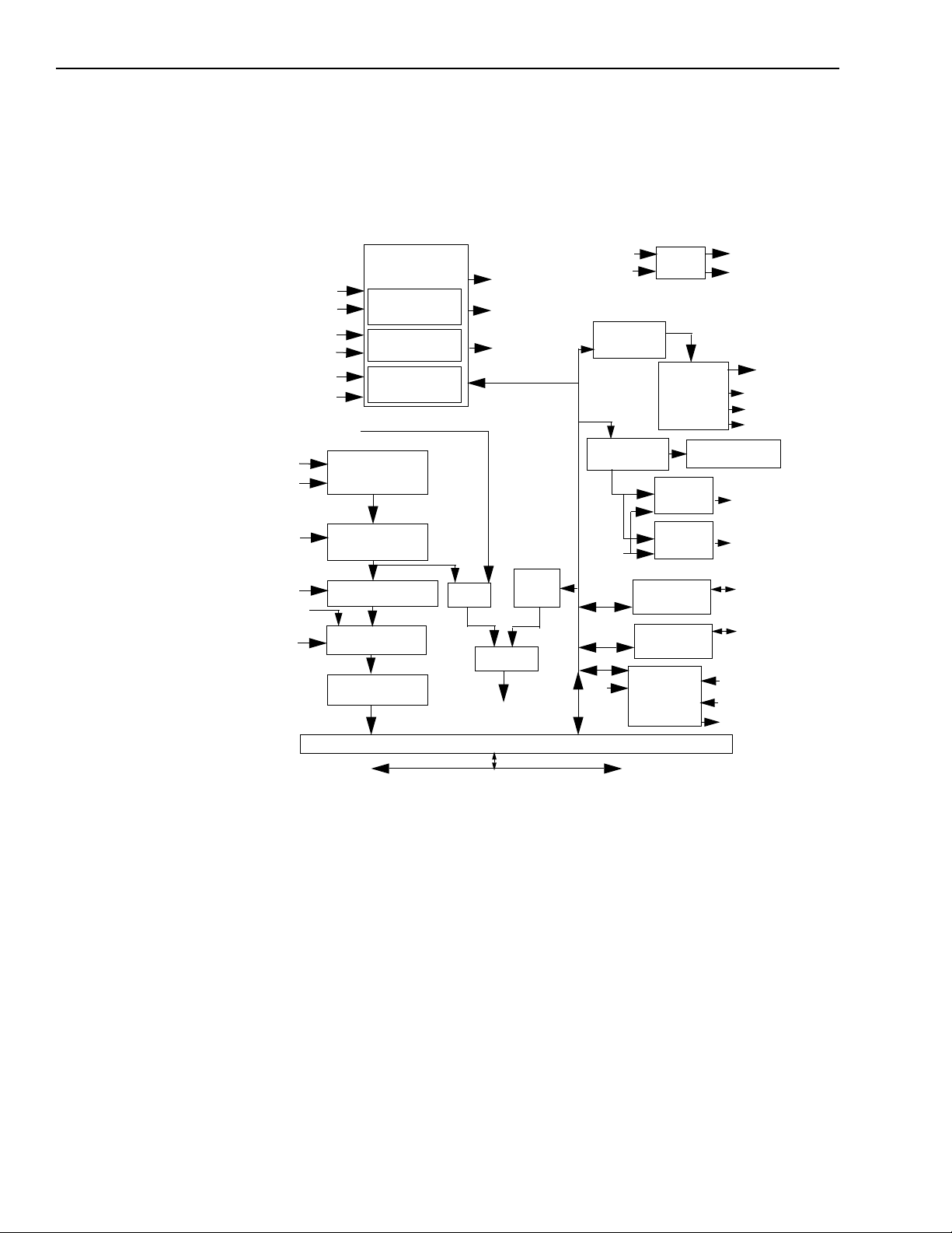
This section describes the analog input, analog output, digital I/O, counter/timer, and synchronous features of the KPCI-3110 and KPCI-3116 boards. To frame the discussions, refer to the
block diagram shown in Figure 2-1. Note that bold entries indicate signals you can access.
Figure 2-1
Block diagram of the KPCI-3110 and KPCI-3116 boards
Ext A/D Clock
Ext A/D TTL Trig
Ext D/A Clock
Ext D/A TTL Trig
Analog Trigger
20MHz Clock
Ext Analog Trigger
Analog In
Ch. Sel
Gain Sel
A/D Clk
DIO Ports
Input Sel
Trigger/Clock
Logic
A/D Counter,
24-bits
D/A Counter
24-bit
TScan Counter
24-bit
32 Channel Mux
Gain Amp
(1, 2, 4, 8)
12- or 16-bit ADC**
Tristate Buffers
1 kSample
Input FIFO
A/D Trig
A/D Clk
D/A Clk
MUX
Analog Trigger
PCI Bus Interface
8-bit
DAC
Compare
A/D Trig
A/D Clk
1 K Entry
CGL FIFO
Output FIFO*
D/A
Clk
4 User
20MHz
Clk
Counter/
Timers,
16-bit ea.
Buffer
CGL Reg.
Channel
Parameter
Reg.
Output FIFO
Counter
12- or 16bit DAC**
12- or 16bit DAC**
Bidirectional
8-bit Latch
Bidirectional
8-bit Latch
A/D Trig Out
A/D Clk Out
Ch. Sel
Gain Sel
Input Sel
Analog Out 1
Analog Out 0
DIO Bank B [7:0]
DIO Bank A [7:0]
User Clk [3:0]
User Gate [3:0]
User Out [3:0]
Analog input features
This section describes the features of the analog input (A/D) subsystem, including the following:
Analog input resolution
Analog input channels
Input ranges and gains
A/D sample clock sources
Analog input conversion modes
Trigger sources and trigger acquisition modes
Data formats and transfer
Error conditions
PCI Bus
*The KPCI-3110 and KPCI-3116 have a 4 kSample Output FIFO;
**Only the KPCI-3116 has a 16-bit ADC and 16-bit DACs.
Page 25

KPCI-3110 and KPCI-3116 User’s Manual Functional Description 2-3
Analog input resolution
The KPCI-3110 board has a fixed analog input resolution of 12 bits. The KPCI-3116 board has a
fixed resolution of 16 bits. The analog input resolution cannot be changed in software.
Analog input channels
KPCI-3110 and KPCI-3116 boards support 32 single-ended or pseudo-differential analog input
channels, or 16 differential analog input channels. Refer to Section 3 for a description of how to
wire these signals. You configure the channel type through DriverLINX software.
NOTE
KPCI-3110 and KPCI-3116 boards can acquire data from a single analog input channel or from
a group of analog input channels. Channels are numbered 0 to 31 for single-ended and pseudodifferential inputs, and 0 to 15 for differential inputs. Refer to “Using DriverLINX with your
hardware: Keithley KPCI-3100 Series” for details of how to specify the channels.
For pseudo-differential inputs, specify single-ended in software; in this
case, how you wire these signals determines the configuration.(Refer to
Section 3 , “ Connecting pseudo-differential voltage inputs .” )
Page 26

2-4 Functional Description KPCI-3110 and KPCI-3116 User’s Manual
Specifying digital input lines in the analog input channel list
In addition to the analog input channels, you can read the two digital I/O channels (16 lines) of
the KPCI-3110 and KPCI-3116 boards using the analog input channel list. This feature is particularly useful when you want to correlate the timing of analog and digital events.
To read these two digital I/O channels, specify channel 0 in the DriverLINX analog input
channel list. Specify the special code (2
13
) in the gain field to indicate that channel 0 is a 16 bit
digital channel. See “Analog Input Termination Modes” in “Using DriverLINX with Your
Hardware.” The hardware-specific gain code is provided in the DriverLINX channel gain list.
You can enter channel 0 anywhere in the list and can enter it more than once, if desired. Refer to
the DriverLINX Analog I/O Programming Guide provided with DriverLINX.
NOTE
If channel 0 is programmed with digital capabilities and is the only
channel in the channel-gain list, the board can read this channel at a
rate of 3 MSamples/s. Refer to the Using DriverLINX with your Hard-
ware:Keithley KPCI-3100 manual provided with DriverLINX .
This channel is treated like any other channel in the analog input channel list; therefore, all the
clocking, triggering, and conversion modes supported for analog input channels are supported
for these digital I/O lines, if you specify them in this manner.
Performing dynamic digital output operations
Using DriverLINX software, you can enable a synchronous dynamic digital output operation for
the A/D subsystem. This feature is particularly useful for synchronizing and controlling external
equipment.
Two dynamic digital output lines are provided: 0 and 1. These lines are set to a value of 0 on
power up; a reset does not affect the values of the dynamic digital output lines. Note that these
lines are provided in addition to the other 16 digital I/O lines. See page 2-21 for more information on the digital I/O features.
To read these two digital I/O lines, specify channel 0 in the DriverLINX analog input channel
list. Specify its digital capabilities in the Digital Capabilities groups of the Logical Device
Descriptor (channel, channel characteristics, and timing and start/stop trigger events). The
hardware-specific gain code is provided in the DriverLINX channel gain list. You can enter
channel 0 anywhere in the list and can enter it more than once, if desired. Refer to the Using
DriverLINX with your Hardware: Keithley KPCI-3100 manual provided with DriverLINX.
NOTE
If channel 0 is programmed with digital capabilities and is the only
channel in the channel-gain list, the board can read this channel at a
rate of 3 MSamples/s. Refer to the Using DriverLINX with your Hard-
ware: Keithley KPCI-3100 manual provided with DriverLINX .
For KPCI-3110 and KPCI-3116 boards, you can specify the following values for the dynamic
digital output lines: 0 (00 in binary format), 1 (01 in binary format), 2 (10 in binary format), or 3
(11 in binary format). Each bit in binary format corresponds to the value to write to the dynamic
digital output line. For example, a value of 1 (01 in binary format) means that a value of 1 is output to dynamic digital output line 0 and value of 0 is output to dynamic output line 1. Similarly,
a value of 2 (10 in binary format) means that a value of 0 is output to dynamic digital output line
0 and value of 1 is output to dynamic output line 1.
For example, assume that the analog input channel list contains channels 5, 6, 7, 8; that dynamic
digital output operations are enabled; and that the values to write to the dynamic digital output
lines are 2, 0, 1, 3. Figure 2-2 shows this configuration.
Page 27
KPCI-3110 and KPCI-3116 User’s Manual Functional Description 2-5
Figure 2-2
An example using dynamic digital outputs
Channel List
5
6
7
8
As analog input channel 5 is read, 1 is output to dynamic digital output line 1, and 0 is output to
dynamic output line 0 (since 2 in binary format is 10). As analog input channel 6 is read, 0 is
output to both dynamic digital output lines. As analog input channel 7 is read, 0 is output to
dynamic digital output line 1, and 1 is output to dynamic output line 0 (since 1 in binary format
is 01). As analog input channel 8 is read, 1 is written to both dynamic digital output lines.
NOTE
Input ranges and gains
Dynamic Digital
Values
2
0
1
3
Dynamic Digital
Outputs
Line 1 Line 0
0
1
0
0
1
0
1
1
Expansion accessories use some of the dynamic digital output signals.
Therefore, you cannot use this feature and an expansion channel in the
same task.
Each channel on the KPCI-3110 or KPCI-3116 board can measure unipolar and bipolar analog
input signals. A unipolar signal is always positive (0 to 10V on KPCI-3110 and KPCI-3116
boards), while a bipolar signal extends between the negative and positive peak values (±10V on
KPCI-3110 and KPCI-3116 boards).
Through DriverLINX software, specify the range as 0 to 10V for unipolar signals or − 10V to
+10V for bipolar signals. Note that the range applies to the entire analog input subsystem, not to
a specific channel.
KPCI-3110 and KPCI-3116 boards also provide gains 1, 2, 4, and 8, which are programmable
per channel. Table 2-1 lists the effective ranges supported by KPCI-3110 and KPCI-3116 boards
using these gains.
Table 2-1
Gains and effective ranges
Gain Unipolar Analog Input Range Bipolar Analog Input Range
1 0 to 10V ±10V
2 0 to 5V ±5V
4 0 to 2.5V ±2.5V
8 0 to 1.25V ±1.25V
For each channel, choose the gain that has the smallest effective range that includes the signal
you want to measure. For example, if the range of your analog input signal is ±1.5V, specify a
range of − 10V to +10V for the board and use a gain of 4 for the channel; the effective input
range for this channel is then ±2.5V, which provides the best sampling accuracy for that channel.
The way you specify gain depends on how you specified the channels, as described in the following subsections.
Page 28

•
•
2-6 Functional Description KPCI-3110 and KPCI-3116 User’s Manual
Specifying the gain for a single channel
The simplest way to specify gain for a single channel is to specify the gain for a single value
analog input operation using software. Refer to page 2-7 for more information on single value
operations.
You can also specify the gain for a single channel using an analog input gain list as described in
the next section.
Specifying the gain for one or more channels
On the KPCI-3110 Series, you can specify the gain for one or more analog input channels using
an analog input gain list. Using software, set up the gain list by specifying the gain for each
entry in the analog input channel-gain list. The gain list parallels the channel list. (The two lists
together are often referred to as the channel-gain list.)
For example, assume the analog input channel list contains three entries: channels 5, 6, and 7;
the gain list might look like this: 2, 4, 1, where a gain of 2 corresponds to channel 5, a gain of 4
corresponds to channel 6, and a gain of 1 corresponds to channel 7.
A/D sample clock sources
KPCI-3110 and KPCI-3116 boards provide two clock sources for pacing analog input operations in continuous mode:
An internal A/D sample clock that uses the 24-bit A/D counter on the board
An external A/D sample clock that you can connect to the screw terminal panel
The A/D sample clock paces the acquisition of each channel in the channel-gain list. This clock
is also called the A/D pacer clock.
NOTE
The following subsections describe the internal and external A/D sample clocks in more detail.
If you specify Digital Capabilities for channel 0 in the channel-gain list,
the A/D sample clock (internal or external) also paces the acquisition of
the 16 digital input lines. Refer to the DriverLINX Analog I/O Program-
ming Guide provided with DriverLINX.
Page 29

•
•
KPCI-3110 and KPCI-3116 User’s Manual Functional Description 2-7
Internal A/D sample clock
The internal A/D sample clock uses a 20MHz time base. Conversions start on the falling edge of
the counter output; the output pulse is active low.
Using software, specify the clock source as internal and the clock frequency at which to pace the
operation. The minimum frequency supported is 1.2Hz (1.2 Samples/s). For the KPCI-3110
boards, the maximum frequency supported is 1.25MHz (1.25 MSamples/s). For the KPCI-3116
board, the maximum frequency supported is 250kHz (250 kSamples/s).
According to sampling theory (Nyquist Theorem), specify a frequency that is at least twice as
fast as the input’s highest frequency component. For example, to accurately sample a 20kHz signal, specify a sampling frequency of at least 40kHz. Doing so avoids an error condition called
aliasing , in which high frequency input components erroneously appear as lower frequencies
after sampling.
NOTE
You can access the output signal from the A/D sample clock using screw
terminal 79 on the STP-3110 screw terminal panel (pin 4 on connector
J2).
External A/D sample clock
The external A/D sample clock is useful when you want to pace acquisitions at rates not available with the internal A/D sample clock or when you want to pace at uneven intervals.
Connect an external A/D sample clock to screw terminal 76 on the STP-3110 screw terminal
panel (pin 7 on connector J2). Conversions start on the falling edge of the external A/D sample
clock input signal.
Using DriverLINX, specify the clock source as external (refer to DriverLINX Analog I/O Pro-
gramming Guide furnished with DriverLINX). For KPCI-3110 and KPCI-3116 boards, the
clock frequency is always equal to the frequency of the external A/D sample clock input signal
that you connect to the board through the screw terminal panel.
Analog input conversion modes
KPCI-3110 and KPCI-3116 boards support the following conversion modes:
Single value polled operations are the simplest to use but offer the least flexibility and effi-
ciency. Use software to specify the range, gain, and analog input channel (among other
parameters); acquire the data from that channel; and convert the result. The data is returned
immediately. For a single value operation, you cannot specify a clock source, trigger source,
trigger acquisition mode, scan mode, or buffer.
Single value operations stop automatically when finished; you cannot stop a single value
operation.
Scan mode takes full advantage of the capabilities of the KPCI-3110 and KPCI-3116
boards. In a scan, you can specify a channel-gain list, clock source, trigger source, trigger
acquisition mode, buffering, and timing. Refer to “Using DriverLINX with Your Hardware:
KPCI-3100 Series” for details on specifying these parameters.
Using DriverLINX software, you can stop a scan when the hardware fills the host buffer you
specified or when your application issues a stop command.
Page 30

2-8 Functional Description KPCI-3110 and KPCI-3116 User’s Manual
Continuously-paced scan mode (rate generation: internal clock)
Use continuously-paced scan mode if you want to accurately control the period between conversions of individual channels in a scan.
When it detects an initial trigger, the board cycles through the channel-gain list, acquiring and
converting the value for each entry in the channel list. This process is defined as the scan. The
board then wraps to the start of the channel-gain list and repeats the process continuously until
either the specified samples are taken or you stop the operation. Refer to page 2-15 for more
information on buffers.
The conversion rate is determined by the frequency of the A/D sample clock. Refer to page 2-6
for more information on the A/D sample clock. The sample rate, which is the rate at which a single entry in the channel-gain list is sampled, is determined by the frequency of the A/D sample
clock divided by the number of entries in the channel-gain list.
NOTE
An A/D Trigger Out signal is provided for your use. This signal is high
when the A/D subsystem is waiting for a trigger and low when a trigger
occurs. In continuously-paced scan mode, this signal goes low when the
trigger occurs and stays low until you stop the operation.
Triggered scan mode
KPCI-3110 and KPCI-3116 boards support two triggered scan (burst) modes: internally-clocked
and externally-clocked. These modes are described in the following subsections.
Internally-retriggered scan mode (internal clock: burst mode)
Use internally-retriggered scan mode if you want to accurately control both the period between
conversions of individual channels in a scan and the period between each scan. This mode is
useful when synchronizing or controlling external equipment, or when acquiring a buffer of data
on each trigger or retrigger. Using this mode, you can acquire up to 262,144 samples per trigger
(256 times per trigger x 1024-location channel-gain list).
When it detects an initial trigger, the board scans the channel-gain list a specified number of
times (up to 256), then waits for an internal retrigger to occur. When the board detects an internal retrigger, the board scans the channel-gain list the specified number of times, then waits for
another internal retrigger to occur. The process repeats continuously until either the specified
samples are taken or you stop the operation.
The sample rate is determined by the frequency of the A/D sample clock divided by the number
of entries in the channel-gain list. Refer to page 2-6 for more information on the A/D sample
clock. The conversion rate of each scan is determined by the frequency of the internal retrigger
clock. The internal retrigger clock is the Triggered Scan Counter, a 24-bit counter with a 20MHz
clock located on the board.
Using DriverLINX software, specify the frequency of the internal retrigger clock. The minimum
retrigger frequency is 1.2Hz. For KPCI-3110 boards, the maximum retrigger frequency is
357.14kHz (357.14 kSamples/s); for KPCI-3116 boards, the maximum retrigger frequency is
166.67kHz (166.666 kSamples/s).
Page 31

•
•
•
•
•
KPCI-3110 and KPCI-3116 User’s Manual Functional Description 2-9
Specify the retrigger frequency as follows:
No. of CGL entries No. of CGLs per trigger×
Min. Retrigger Period
----------------------------------------------------------------------------------------------------------------2µs+
=
A/D sample clock frequency
Max. Retrigger
-------------------------------------------------------------------------------=
Frequency Min. Retrigger Period
1
For example, if you are using 512 channels in the channel-gain list (CGL), scanning the channelgain list 256 times every trigger or retrigger, and using an A/D sample clock with a frequency of
1MHz, set the maximum retrigger frequency to 7.62Hz, since:
7.62Hz
--------------------------------------------------=
-----------------------------2µs+
1
512 256×()
MHz
To select internally-retriggered scan mode, use software to specify the following parameters:
The dataflow as continuous, continuous pre-trigger, or continuous about-trigger.
Triggered scan mode usage as enabled.
The retrigger mode as internal.
The number of times to scan per trigger or retrigger (also called the multiscan count).
The frequency of the retrigger clock.
The initial trigger source depends on the trigger acquisition mode selected. Refer to page 2-10
for more information on the supported trigger acquisition modes and trigger sources.
NOTE
An A/D Trigger Out signal is provided for your use. This signal is high
when the A/D subsystem is waiting for a trigger and low when a trigger
occurs. In internally-retriggered scan mode, this signal stays low until
the desired number of samples have been acquired, then goes high until
the internal retrigger is generated.
Externally-retriggered scan mode (external clock: burst mode)
Use externally-retriggered scan mode if you want to accurately control the period between conversions of individual channels and retrigger the scan based on an external event. Like internally-retriggered scan mode, this mode allows you to acquire 262,144 samples per trigger (256
times per trigger x 1024-location channel-gain list).
NOTE
Use externally-retriggered scan mode with continuous post-trigger
acquisitions only. Refer to page 2-11 for more information on post-trig-
ger acquisitions.
When a KPCI-3110 or KPCI-3116 board detects an initial trigger (post-trigger source only), the
board scans the channel-gain list up to 256 times, then waits for an external retrigger to occur.
Specify any supported post-trigger source as the initial trigger. For the retrigger, specify either
an external digital (TTL) trigger or an external analog threshold trigger.
When the retrigger occurs, the board scans the channel-gain list the specified number of times,
then waits for another external retrigger to occur. The process repeats continuously until either
the allocated buffers are filled or you stop the operation. Refer to page 2-15 for more information on buffers.
Page 32

•
•
•
•
•
•
•
•
•
2-10 Functional Description KPCI-3110 and KPCI-3116 User’s Manual
The conversion rate of each channel is determined by the frequency of the A/D sample clock.
Refer to page 2-6 for more information on the A/D sample clock. The conversion rate of each
scan is determined by the period between external retriggers; therefore, it cannot be accurately
controlled. The board ignores external triggers that occur while it is acquiring data. Only external retrigger events that occur when the board is waiting for a retrigger are detected and acted
on.
To select externally-retriggered scan mode, use software to specify the following parameters:
The dataflow as continuous (post-trigger).
Triggered scan mode as enabled.
The retrigger mode as an external retrigger.
The number of times to scan per trigger or retrigger (also called the multiscan count).
The retrigger source as the external digital (TTL) trigger or an external analog threshold
trigger.
Triggers
A trigger is an event that occurs based on a specified set of conditions. KPCI-3110 and
KPCI-3116 boards support a number of trigger sources and trigger acquisition modes, described
in the following subsections.
Trigger sources
KPCI-3110 and KPCI-3116 boards support the following trigger sources:
Software trigger
External digital (TTL) trigger
Analog threshold trigger
This subsection describes these trigger sources in more detail.
Software trigger
A software trigger event occurs when you start the analog input operation (the computer issues a
write to the board to begin conversions). Specify the software trigger source in software.
External digital (TTL) trigger
For analog input operations, an external digital trigger event occurs when the KPCI-3110 or
KPCI-3116 board detects either a rising or falling edge on the external A/D TTL trigger input
signal connected to screw terminal 77 on the STP-3110 screw terminal panel (pin 6 of connector
J2). The trigger signal is TTL-compatible.
Using software, specify the trigger source as a rising-edge external digital trigger or a fallingedge external digital trigger.
Analog threshold trigger
For analog input operations, an analog trigger event occurs when the KPCI-3110 or KPCI-3116
detects a transition from above a threshold level to below a threshold level (falling edge), or a
transition from below a threshold level to above a threshold level (rising edge). The following
analog threshold trigger sources are available:
External Analog Trigger input signal is connected to screw terminal TB107 (Analog
Trigger) on the STP-3110 screw terminal panel (pin 34 on connector J2). Using software,
Page 33

•
•
KPCI-3110 and KPCI-3116 User’s Manual Functional Description 2-11
perform the following steps to configure a scan triggered by an external analog trigger input
signal:
1. Specify the trigger source as either a rising-edge or falling-edge analog threshold trigger.
2. Specify channel 0 as the trigger channel. To distinguish this channel from analog input channel
0, set the special gain code of &H8000 to indicate the use of the dedicated Analog Trigger line.
When channel 0 is scanned, the analog trigger signal at TB107 is detected to start the acquisition
process.
One of the analog input channels after gain is applied (also called the output of the pro-
grammable gain amplifier (PGA). Using software, specify the trigger source as either a positive threshold trigger or negative threshold trigger.
Using DriverLINX software, specify the analog input channel used as the analog threshold trigger as the first channel in the channel list; refer to page 2-3 for more information.
On KPCI-3110 and KPCI-3116 boards, the threshold level is set using a dedicated 8-bit DAC;
the hysteresis is fixed at 50mV. Using software, program the threshold level by writing a voltage
value to this DAC; this value can range from − 10V to +10V.
•
NOTE
If you are using an analog threshold trigger to trigger both the A/D and
the D/A subsystems, ensure that you use the same analog trigger type for
both subsystems (either external or one of the analog input channels).
Trigger acquisition modes
KPCI-3110 and KPCI-3116 boards can acquire data in post-trigger mode, pre-trigger mode, or
about-trigger mode. These trigger acquisition modes are described in more detail in the following subsections.
Post-trigger acquisition
Use post-trigger acquisition mode (continuous mode) when you want to acquire data when a
post-trigger or retrigger, if using triggered scan mode, occurs.
Using DriverLINX software, specify the following parameters:
The dataflow as continuous.
The trigger source to start the post-trigger acquisition (the post-trigger source) as any of the
supported trigger sources.
Refer to page 2-7 for more information on the supported conversion modes. Refer to page 2-10
for information on the supported trigger sources.
Post-trigger acquisition starts when the board detects the post-trigger event and stops when the
specified number of post-trigger samples has been acquired, or when you stop the operation.
If you are using triggered scan mode, the board continues to acquire post-trigger data using the
specified retrigger source to clock the operation. Refer to page 2-8 for more information on triggered scan mode.
Figure 2-3 illustrates continuous post-trigger mode using a channel-gain list with three entries:
channel 0, channel 1, and channel 2. Triggered scan mode is disabled. In this example, post-trigger
analog input data is acquired on each clock pulse of the A/D sample clock. The board wraps to the
beginning of the channel-gain list and repeats continuously (continuously-paced scan mode).
Figure 2-3
Continuous post-trigger mode without triggered scan
Chan 0
Chan 1
A/D
Sample
Post-trigger Event Occurs
Chan 2
Chan 0
Chan 1
Chan 2
Chan 0
Post-trigger Data Acquired Continuously
Chan 2
Chan 1
Chan 0
Chan 2
Chan 1
Page 34

2-12 Functional Description KPCI-3110 and KPCI-3116 User’s Manual
Figure 2-4 illustrates the same example using triggered scan mode (either internally- or exter-
nally-retriggered). The multiscan count is 2 indicating that the channel-gain list will be scanned
twice per trigger or retrigger. In this example, post-trigger analog input data is acquired on each
clock pulse of the A/D sample clock until the channel-gain list has been scanned twice; then, the
board waits for the retrigger event. When the retrigger event occurs, the board scans the channelgain list twice more, acquiring data on each pulse of the A/D sample clock. The process repeats
continuously with every specified retrigger event.
Figure 2-4
Continuous post-trigger mode with triggered scan
Chan 0
A/D
Sample
Post-trigger event occurs;
post-trigger data acquired for
two scans of the CGL.
Chan 2
Chan 1
Chan 0
Board waits for
retrigger event.
Chan 2
Chan 1
Chan 2
Chan 0
Chan 1
Retrigger event occurs;
post-trigger data acquired for
two scans of the CGL.
Chan 0
Chan 2
Chan 1
Pre-trigger Acquisition
Use pre-trigger acquisition mode (continuous pre-trigger mode) when you want to acquire data
before a specific external event occurs.
Using software, specify the following parameters:
• The dataflow as continuous pre-trigger
• The pre-trigger source as the software trigger
• The post-trigger source as the external digital (TTL) trigger or the external analog threshold
trigger
• If you are using triggered scan mode, the retrigger mode as the internal retrigger
Refer to page 2-7 for more information on the supported conversion modes. Refer to page 2-10
for information on the supported trigger sources.
When using pre-trigger acquisition, you cannot use an external retrigger in triggered scan mode.
Refer to page 2-8 for more information on triggered scan mode.
Pre-trigger acquisition starts when you start the operation and stops when the board detects the
selected post-trigger source, indicating that the first post-trigger sample was acquired (this sample is ignored).
If you are using internally-retriggered scan mode and the post-trigger event has not occurred, the
board continues to acquire pre-trigger data using the internal retrigger clock to clock the operation. When the post-trigger event occurs, the operation stops. Refer to page 2-8 for more information on internally-retriggered scan mode.
Figure 2-5 illustrates continuous pre-trigger mode using a channel-gain list of three entries:
channel 0, channel 1, and channel 2. In this example, pre-trigger analog input data is acquired on
each clock pulse of the A/D sample clock. The board wraps to the beginning of the channel-gain
list and the acquisition repeats continuously until the post-trigger event occurs. When the posttrigger event occurs, acquisition stops.
Page 35

KPCI-3110 and KPCI-3116 User’s Manual Functional Description 2-13
Figure 2-5
Continuous pre-trigger mode
Chan 0
Chan 1
A/D
Sample
Pre-trigger Event Occurs
Chan 2
Pre-trigger Data Acquired
Chan 0
Chan 2
Chan 0
Chan 1
Post-trigger Event Occurs
Acquisition Stops
Figure 2-6 illustrates the same example using internally-retriggered triggered scan mode. The
multiscan count is 2 indicating that the channel-gain list will be scanned twice per trigger or
retrigger. In this example, pre-trigger analog input data is acquired on each clock pulse of the
A/D sample clock until the channel-gain list has been scanned twice; then, the board waits for
the internal retrigger event. When the internal retrigger occurs, the process repeats. The process
stops when the post-trigger event occurs.
Figure 2-6
Continuous pre-trigger mode with triggered scan
Chan 2
Chan 0
A/D
Sample
Chan 0
Chan 1
Chan 2
Chan 0
Chan 1
Chan 2
Chan 0
Chan 1
Pre-trigger event occurs;
pre-trigger data is acquired
for two scans of the CGL.
Board waits for
retrigger event.
Retrigger event occurs;
pre-trigger data is
acquired until post-trigger
event occurs.
Post-trigger event
occurs; acquisition
stops.
About-trigger acquisition
Use about-trigger acquisition mode (continuous about-trigger mode) when you want to acquire
data both before and after a specific external event occurs. This operation is equivalent to doing
both a pre-trigger and a post-trigger acquisition.
Using software, specify the following parameters:
• The dataflow as continuous about-trigger
• The pre-trigger source as the software trigger
• The post-trigger source as the external digital (TTL) trigger or the external analog threshold
trigger
• If you are using triggered scan mode, the retrigger mode as the internal retrigger
Refer to page 2-7 for more information on the supported conversion modes. Refer to page 2-10
for information on the supported trigger sources.
When using about-trigger acquisition, you cannot use an external retrigger in triggered scan
mode. Refer to page 2-8 for more information on triggered scan mode.
Page 36

2-14 Functional Description KPCI-3110 and KPCI-3116 User’s Manual
The about-trigger acquisition starts when you start the operation. When the board detects the
selected post-trigger event, the board stops acquiring pre-trigger data and starts acquiring posttrigger data.
If you are using internally-retriggered scan mode and the post-trigger event has not occurred, the
board continues to acquire pre-trigger data using the internal retrigger clock to clock the operation. If, however, the post-trigger event has occurred, the board continues to acquire post-trigger
data using the internal retrigger clock to clock the operation.
The about-trigger operation stops when the specified number of post-trigger samples has been
acquired, or when you stop the operation. Refer to page 2-8 for more information on internallyretriggered scan mode.
Figure 2-7 illustrates continuous about-trigger mode using a channel list of two entries: channel
0 and channel 1. In this example, pre-trigger analog input data is acquired on each clock pulse of
the A/D sample clock, scanning the channel list continuously, until the post-trigger event occurs.
When the post-trigger event occurs, post-trigger analog input data is acquired continuously on
each clock pulse of the A/D sample clock.
Figure 2-7
Continuous about-trigger mode
Chan 0
Chan 1
A/D
Sample
Pre-trigger Event Occurs
Chan 0
Chan 1
Pre-trigger Data Acquired
Chan 0
Chan 1
Post-trigger Event Occurs
Chan 0
Chan 0
Chan 1
Chan 1
Post-trigger Data Acquired
Chan 0
Chan 1
. . .
Figure 2-8 illustrates the same example using internally-retriggered triggered scan mode. The
multiscan count is 2 indicating that the channel-gain list will be scanned twice per trigger or
retrigger. In this example, pre-trigger analog input data is acquired on each clock pulse of the
A/D sample clock for two scans; then, the board waits for the internal retrigger event. When the
internal retrigger occurs, the board begins acquiring pre-trigger data until the post-trigger event
occurs. Then, the board finishes scanning the channel-gain list the specified number of times, but
acquires the data as post-trigger samples. On all subsequent internal retriggers, post-trigger data
is acquired.
Figure 2-8
Continuous about-trigger mode with triggered scan
Chan 0
Chan 1
A/D
Sample
Chan 0
Chan 1
Chan 0
Chan 1
Chan 0
Chan 1
Chan 0
Chan 1
Pre-trigger event occurs;
pre-trigger data is
acquired for 2 scans of
the CGL.
Re-trigger event
occurs; pre-trigger
data is acquired until
post-trigger occurs.
Post-trigger event occurs;
post-trigger data is
acquired until the end of
the number of scans.
Re-trigger event occurs;
post-trigger data is
acquired for 2 scans of
the CGL.
Page 37

KPCI-3110 and KPCI-3116 User’s Manual Functional Description 2-15
Data format and transfer
KPCI-3110 and KPCI-3116 boards use offset binary data encoding to represent signals. In
DriverLINX software, the analog input value is returned as a code or voltage depending on user
input. DriverLINX provides single-value and buffer methods to convert between voltages and
analog codes. The single-value functions are Volts2Code and Code2Volts. Refer to DriverLINX
manuals provided with DriverLINX for more information.
To represent unipolar signals, KPCI-3110 and KPCI-3116 boards use straight binary data encoding, such as 000 (for 12-bit boards) or 0000 (for 16-bit boards) to represent 0V, and FFFh (for
12-bit boards) or FFFFh (for 16-bit boards) to represent full-scale. To represent bipolar signals,
KPCI-3110 and KPCI-3116 boards use offset binary data encoding, such as 000 (for 12-bit
boards) or 0000 (for 16-bit boards) to represent negative full-scale, and FFFh (for 12-bit boards)
or FFFFh (for 16-bit boards) to represent positive full-scale. Use software to specify the data
encoding as binary.
DriverLINX transfers data to the controlling (your program) application in buffers that the application has allocated. The size and number of buffers that your application should allocate is a
function of Windows’ message processing and the type of stop event you have specified.
Guidance on specifying buffers
If using ‘Stop on terminal count,’ data transfer stops automatically after the specified buffer is
filled. Only a single buffer of adequate length is needed.
If using ‘Stop on trigger’ (analog or digital) or ‘Stop on command,’ the data transfer will continue indefinitely until the stop condition occurs, with buffers being used and reused to keep up
with incoming transfers. In this case, allocate enough buffers for one second’s worth of data,
plus two extras to provide a margin for recycling of used buffers. (The total number of buffers
available should equal [(Sampling Frequency / Buffer Size) + 2].)
A Windows message will be sent each time a buffer is filled. For example, at a rate of 100Hz
and a buffer of 100 samples, a buffer filled message will be sent once per second. A buffer message rate in the range of 1 – 10 per second is recommended to avoid overloading Windows with
too many messages.
Error conditions
KPCI-3110 and KPCI-3116 boards can report the following analog input error conditions to the
host computer:
• A/D Over Sample — Indicates that the A/D sample clock rate is too fast. This error is
reported if a new A/D sample clock pulse occurs while the ADC is busy performing a conversion from the previous A/D sample clock pulse. The host computer can clear this error. To
avoid this error, use a slower sampling rate.
• Input FIFO Overflow — Indicates that the analog input data is not being transferred fast
enough from the Input FIFO across the PCI bus to the host computer. This error is reported
when the Input FIFO becomes full; the board cannot get access to the PCI bus fast enough.
The host computer can clear this error, but the error will continue to be generated if the Input
FIFO is still full. To avoid this error, close other applications that may be running while you
are acquiring data. Also check if bus mastering is evaluated in B105. If this has no effect, try
using a computer with a faster processor or reduce the sampling rate.
• Host Block Overflow — Indicates that the host computer is not handling data from the
board fast enough. This error is reported if the board completes the transfer of a block of
input data to the circular buffer in the host computer before the host computer has finished
reading the last block of data.
If any of these error conditions occurs, the board stops acquiring and transferring data to the host
computer.
NOTE DriverLINX reports any of these errors as a “DATA LOST” message.
Page 38

2-16 Functional Description KPCI-3110 and KPCI-3116 User’s Manual
Analog output features
Two analog output (D/A) subsystems are provided on KPCI-3110 and KPCI-3116 boards. The
first D/A subsystem contains the majority of analog output features. The second is dedicated to
threshold triggering only (refer to page 2-18 for information on analog threshold triggering).
This section describes the following features of the first D/A subsystem:
• Analog output resolution
• Analog output channels
• Output ranges and gains
• Output filters
• D/A output clock sources
• Trigger sources
• Analog output conversion modes
• Data formats and transfer
• Error conditions
Analog output resolution
KPCI-3110 boards have a fixed analog output resolution of 12 bits. The KPCI-3116 boards have
a fixed analog output resolution of 16 bits. The analog output resolution cannot be changed in
software.
Analog output channels
KPCI-3110 and KPCI-3116 boards support two differential analog output channels (DAC0 and
DAC1). Refer to Section 3 for information on how to wire analog output signals to the board
using the screw terminal panel.
Within each DAC, the digital data is double buffered to prevent spurious outputs, then output as
an analog signal. Both DACs power up to a value of 0V ±10mV. Note that resetting the board
does not clear the values in the DACs.
KPCI-3110 and KPCI-3116 boards can output data from a single analog output channel or from
two analog output channels. The following subsections describe how to specify the channels.
Specifying a single channel
The simplest way to output data to a single analog output channel is to specify the channel for a
single value analog output operation using software; refer to page 2-19 for more information on
single value operations.
You can also specify a single analog output channel using an analog output channel list,
described in the next section.
Specifying one or more channels
You can specify one or two analog output channels in the analog output channel list, either starting with DAC 0 or with DAC 1.
Values are output simultaneously to the entries in the channel list.
Page 39

KPCI-3110 and KPCI-3116 User’s Manual Functional Description 2-17
Output filters
On the KPCI-3116 board only, each DAC supports a software-selectable, single-pole, filter of
20kHz. Specifying a 20kHz filter is useful if you want to smooth the output values of the DAC.
On power-up or reset, no filter is used. Refer to DriverLINX manuals for more information on
filters.
Output ranges and gains
Each DAC on the KPCI-3110 or KPCI-3116 board can output bipolar analog output signals in
the range of ±10V.
In DriverLINX software, specify a gain of -1 for bipolar analog output operations. This sets both
range and gain.
If you are using an analog output channel list, the subsystem defaults to a gain of 1 for each
channel; therefore, you do not have to specify the gain.
D/A output clock sources
KPCI-3110 and KPCI-3116 boards provide two clock sources for pacing the output of each
channel in the analog output channel-gain list:
• An internal D/A output clock that uses the 24-bit D/A Counter on the board.
• An external D/A output clock that you can connect to the screw terminal panel
The following subsections describe the internal and external D/A output clocks in more detail.
Internal D/A output clock
The internal D/A output clock uses a 20MHz time base. Conversions start on the falling edge of
the counter output; the output pulse is active low.
Through software, specify the clock source as internal and the clock frequency at which to pace
the analog output operation. The minimum frequency supported is 1.2Hz (1.2 Samples/s). For
KPCI-3110 boards, the maximum frequency supported is 500kHz (500 kSamples/s). For KPCI3116 boards, the maximum frequency supported is 200kHz (200 kSamples/s). See page 2-19 for
more information on these conversion modes.
External D/A output clock
The external D/A output clock is useful when you want to pace analog output operations at rates
not available with the internal D/A output clock, if you want to pace at uneven intervals, or if
you want to start pacing when an external event occurs.
Connect an external D/A output clock to screw terminal 74 on the STP-3110 screw terminal
panel (pin 9 on connector J2). Conversions start on the falling edge of the external D/A output
clock signal.
Using software, specify the clock source as external. For KPCI-3110 and KPCI-3116 boards, the
clock frequency is always equal to the frequency of the external D/A output clock input signal
that you connect to the board through the screw terminal panel.
Page 40

2-18 Functional Description KPCI-3110 and KPCI-3116 User’s Manual
Trigger sources
A trigger is an event that occurs based on a specified set of conditions. KPCI-3110 and
KPCI-3116 boards support the following trigger sources for analog output operations:
• Software trigger
• External digital (TTL) trigger
• Analog threshold trigger
This subsection describes these trigger sources in more detail.
Software trigger
A software trigger event occurs when you start the analog output operation (the computer issues
a write to the board to begin conversions). Specify the software trigger source in software.
External digital (TTL) trigger
For analog output operations, an external digital trigger event occurs when the KPCI-3110 or
KPCI-3116 board detects either a rising or falling edge on the External D/A TTL Trigger input
signal connected to screw terminal 75 on the STP-3110 screw terminal panel (pin 8 on connector
J2). The trigger signal is TTL-compatible.
Using software, specify the trigger source as either a rising-edge external digital trigger or
falling-edge external digital trigger.
Analog threshold trigger
For analog output operations, an analog trigger event occurs when the KPCI-3110 or KPCI-3116
board detects a transition from above a threshold level to below a threshold level (falling edge),
or a transition from below a threshold level to above a threshold level (rising edge). The following analog threshold trigger sources are available:
• External Analog Trigger input signal connected to screw terminal 104 on the STP-3110
screw terminal panel (pin 34 on connector J2). Using software, specify the trigger source as
either a rising-edge or falling-edge analog threshold trigger.
• One of the analog input channels after gain is applied. Using software, specify the trigger
source as either a positive threshold trigger or a negative threshold trigger.
Using software, specify the analog input channel used as the analog threshold trigger as the first
channel in the analog input channel list; refer to page 2-3 for more information.
On KPCI-3110 and KPCI-3116 boards, the threshold level is set using a dedicated 8-bit DAC
(the second analog output subsystem); the hysteresis is fixed at 50mV. Using software, program
the threshold level by writing a voltage value to the DAC of the second analog output subsystem;
this value can range from −10V to +10V.
NOTE If you are using an analog threshold trigger to trigger both the A/D and
the D/A subsystems, ensure that you use the same analog trigger type for
both subsystems (either external or one of the analog input channels).
Page 41

KPCI-3110 and KPCI-3116 User’s Manual Functional Description 2-19
Analog output conversion modes
KPCI-3110 and KPCI-3116 boards support the following conversion modes:
• Single value (polled) operations are the simplest to use but offer the least flexibility and
efficiency. Use software to specify the range, gain, and analog output channel (among other
parameters), and output the data from that channel. For a single value operation, you cannot
specify a clock source, trigger source, or buffer.
Single value operations stop automatically when finished; you cannot stop a single value
operation.
• Continuous analog output operations take full advantage of the capabilities of the
KPCI-3110 and KPCI-3116 boards. In this mode, you can specify an analog output channelgain list, clock source, trigger source, buffer, and buffer wrap mode. Two continuous analog
output operations are supported: continuously-paced and waveform generation mode. These
modes are described in the following subsections.
Using DriverLINX software, you can stop a scan when the hardware fills the host buffer you
specified or when your application issues a stop command.
Continuously-paced analog output
Use continuously-paced analog output mode if you want to accurately control the period
between conversions of individual analog output channels in the analog output channel list.
The host computer transfers digital values to write to the DACs from allocated circular buffers in
computer memory to the Output FIFO on the board. KPCI-3110 and KPCI-3116 boards have a 4
kSample Output FIFO. Use software to allocate the number of buffers and to specify the values.
When it detects a trigger, the board outputs the values in the Output FIFO to the DACs at the
same time. Even samples (0, 2, 4, and so on) are written to entry 0 in the channel list; odd samples (1, 3, 5, and so on) are written to entry 1 in the channel list. The operation repeats continuously until either all the data is output from the buffers (if buffer wrap mode is none) or if you
stop the operation (if buffer wrap mode is multiple). Refer to page 2-20 for more information on
buffers.
Ensure that the host computer transfers data to the Output FIFO fast enough so that the Output
FIFO does not empty completely; otherwise, an Output FIFO Underrun error results. Note that
the Output FIFO Counter increments each time the host loads a value into the Output FIFO and
decrements each time the DAC reads a value from the Output FIFO; the counter is reset to 0
when the Output FIFO is reset. To avoid the Output FIFO Underrun error in continuously-paced
mode, the host computer can read the Output FIFO Counter to determine how many samples
remain in the Output FIFO, and transfer more data before the Output FIFO empties.
The conversion rate is determined by the frequency of the D/A output clock. For KPCI-3110
boards, the maximum throughput rate in this mode is 500 (500 kSamples/s) in 100mV steps. For
KPCI-3116 boards, the maximum throughput rate in this mode is 200kHz (200 kSamples/s) in
100mV steps. Note that rate is system dependent. Refer to page 2-17 for more information on
the D/A output clock.
Page 42

2-20 Functional Description KPCI-3110 and KPCI-3116 User’s Manual
Waveform generation
Use waveform generation mode if you want to output waveforms repetitively.
Before this process can begin, the host computer must transfer the entire waveform pattern to
output to the DACs from computer memory into the Output FIFO on the board.
For the KPCI-3110 and KPCI-3116 boards, if you are using a single DAC, the waveform pattern
can range from 2 to 4,096 samples. If you are using two DACs, the waveform pattern can range
from 2 to 2,048 samples.
When it detects a trigger, the board cycles through the analog output channel-gain list, converting and outputting the specified waveform for the specified DACs. When the Output FIFO empties, the board issues a retransmit pulse to the Output FIFO. This allows the board to output the
same pattern continuously to the DACs without having to reload the Output FIFOs. Refer to
page 2-20 for more information on buffers.
The conversion rate is determined by the frequency of the D/A output clock. For KPCI-3110
boards, the maximum throughput rate in this mode is 500kHz (500 kSamples/s) in 100mV steps.
For the KPCI-3116 boards, the maximum throughput rate in this mode is 200kHz
(200 kSamples/s) in 100mV steps. Refer to page 2-17 for more information on the D/A output
clock.
To select waveform generation mode, refer to the “Using DriverLinx with your hardware:
KPCI-3100 Series” manual.
Data format and transfer
Data from the host computer must use offset binary data encoding for analog output signals.
DriverLINX converts this “native format” to a hardware-independent format so that applications
can use the numeric operations that are intrinsic to most high-level languages. A DriverLINX
Service Request may be used for several types of data conversion (such as VOLTS2CODE conversion that converts analog voltage to D/A code). Because the data values depend on the
selected gain at the time of the data transfer, you should use DriverLINX to convert the data, as
it takes the gain properties of the Service Request into account.
NOTE Refer to the DriverLINX Analog I/O Programming Guide and the
“Using DriverlINX with your Hardware” manuals furnished with
DriverLINX.
Error conditions
KPCI-3110 and KPCI-3116 boards can report an Output FIFO Underflow error to the host computer. This error indicates that the analog output data was not being transferred fast enough
across the PCI bus from the host computer to the Output FIFO on the board.
If the D/A output clock occurs while the Output FIFO is empty, an error is not reported since the
most likely cause is that the host computer has no more data to output. In this case, the last value
received from the host computer is output by the specified DACs continuously until the board is
powered down or new data becomes available. If, however, the host does an additional write to
the Output FIFO (after the D/A output clock occurred while the Output FIFO was empty), the
data is written to the DACs and the Output FIFO Underflow error is reported. This error has no
effect on board operation; the host computer can clear this error.
Page 43

KPCI-3110 and KPCI-3116 User’s Manual Functional Description 2-21
To avoid this error, ensure that the host computer provides data to the Output FIFO faster than
the DACs are converting the data. You can read the value of the Output FIFO Counter to determine how many samples are in the Output FIFO.
If this error condition occurs, the board stops acquiring and transferring data to the host
computer.
NOTE DriverLINX reports this error as a “DATA LOST” message.
Digital I/O features
This section describes the following features of the digital I/O subsystem:
• Digital I/O lines
• Digital I/O resolution
• Digital I/O operation modes
Digital I/O lines
KPCI-3110 and KPCI-3116 boards support 16 digital I/O lines through the digital input (DIN)
and output (DOUT) subsystems; both subsystems use the same digital I/O lines. These lines are
divided into two banks of eight: Bank A, lines 0 to 7; and Bank B, lines 0 to 7. You can use each
bank as either an input port or an output port; all eight lines within a bank have the same configuration. For example, if you use Bank A as an input port (port 0), lines 0 to 7 of Bank A are configured as inputs. Likewise, if you use Bank B as an output port (port 1), lines 0 to 7 of Bank B
are configured as outputs.
Specify the digital I/O line to read or write in a single value digital I/O operation. Refer to
page 2-22 for more information on single value operations.
On power up or reset, no digital data is output from the board.
DriverLINX lets you dynamically reconfigure digital I/O ports at run time using a “Digital Setup
Event.” Refer to DriverLINX Digital I/O Programming Guide for information and limitations of
this function.
Page 44

2-22 Functional Description KPCI-3110 and KPCI-3116 User’s Manual
Digital I/O operation modes
DriverLINX uses the Digital I/O Subsystem for single value outputs. For continuous digital
input, DriverLINX uses the Analog I/O subsystem (see “Specifying digital input lines in the ana-
log input channel list” on page 2-4. Single value operations stop automatically when finished;
you cannot stop a single value operation
• Continuous digital input takes full advantage of the capabilities of the KPCI-3110 or
KPCI-3116 board. Program the digital input lines as Analog Input Channel 0; enter the
inputs through the DriverLINX A/D subsystem. You will assign a special gain code to this
channel to distinguish it as digital. You can specify parameters such as clock source, scan
mode, and trigger source for the digital input operation. Refer to page 2-4 for more
information on specifying digital input lines for a continuous digital input operation. Refer to
DriverLINX Analog I/O Programming Guide and Using DriverLINX with your Hardware
manuals that accompany DriverLINX.
• Dynamic digital output is useful for synchronizing and controlling external equipment and
allows you to output data to two dynamic digital output lines each time an analog input value
is acquired. This mode is programmed through the A/D subsystem; refer to page 2-4 for
more information.
NOTE Expansion accessories use some of the dynamic digital output signals.
Therefore, you cannot use this feature and an expansion channel in the
same task.
Counter/timer features
The counter/timer circuitry on the board provides the clocking circuitry used by the A/D and
D/A subsystems as well as several user counter/timer features. This section describes the following user counter/timer features:
• Units
• C/T clock sources
• Gate types
• Pulse types and duty cycles
• Counter/timer operation modes
Units
KPCI-3110 and KPCI-3116 boards support four user 16-bit counter/timer units (called
counters); counters are numbered 0, 1, 2, and 3.
Each counter accepts a clock input signal and gate input signal and outputs a clock output signal
(also called a pulse output signal), as shown in Figure 2-9.
Page 45

KPCI-3110 and KPCI-3116 User’s Manual Functional Description 2-23
Figure 2-9
Counter/timer channel
Clock Input Signal
(internal, external, or
internally cascaded)
C/T clock sources
The following clock sources are available for the user counters:
• Internal C/T clock
• External C/T clock
• Internally cascaded clock
Refer to the following subsections for more information on these clock sources.
Internal C/T clock
The internal C/T clock uses a 20MHz time base. Counter/timer operations start on the rising
edge of the clock input signal.
Counter
Gate Input Signal
(software or
external input)
Pulse Output
Signal
Through software, specify the clock source as internal and the frequency at which to pace the
counter/timer operation (this is the frequency of the clock output signal). The maximum frequency that you can specify for the clock output signal is 10MHz. The minimum frequency that
you can specify for the clock output signal is 305.18Hz.
External C/T clock
The external C/T clock is useful when you want to pace counter/timer operations at rates not
available with the internal C/T clock or if you want to pace at uneven intervals. The rising edge
of the external C/T clock input signal is the active edge.
Using DriverLINX, specify the clock source as external and the clock divider used to determine
the frequency at which to pace the operation (this is the frequency of the clock output signal).
The minimum clock divider that you can specify is 2.0; the maximum clock divider that you can
specify is 65,536. For example, if you supply an external C/T clock with a frequency of 5MHz
and specify a clock divider of 5, the resulting frequency of the external C/T clock output signal
is 1MHz. The resulting frequency of the external C/T clock output signal must not exceed
2.5MHz.
Page 46

2-24 Functional Description KPCI-3110 and KPCI-3116 User’s Manual
Connect the external C/T clock to the board through the STP-3110 screw terminal panel.
Table 2-2 lists the screw terminals that correspond to the external C/T clock signals of each
counter/timer.
Table 2-2
External C/T clock signals
Screw Terminal on
Counter/Timer
0 TB58 17
1 TB62 15
2 TB66 13
3 TB70 11
STP-3110
Pin on
Connector J2
Internally cascaded clock
You can also internally route the clock output signal from one user counter to the clock input
signal of the next user counter to internally cascade the counters. In this way, you can create a
32-bit counter without externally connecting two counters together. KPCI-3110 and KPCI-3116
boards support software cascading on counters 0 and 1, 1 and 2, and 2 and 3.
Specify internal cascade mode in software. The rising edge of the clock input signal is active.
To specify internal cascading, use DriverLINX software to set the internal cascade mode, then
specify the clock input and gate input for the first counter in the cascaded pair. Specify the clock
source of the second counter as C/T
clock input signal of the second counter. For example, if counters 1 and 2 are cascaded, specify
the clock input and gate input for counter 1.
The maximum frequency that you can specify for the clock output signal is 10MHz. For a 32-bit
cascaded counter, the minimum frequency that you can specify for the clock output signal is
0.00465Hz, which corresponds to a rate of once every 215 seconds.
. The clock output signal from the first counter is the
N-1
Gate types
The active edge or level of the gate input to the counter enables counter/timer operations. The
operation starts when the clock input signal is received. KPCI-3110 and KPCI-3116 boards provide the following gate input types:
• None — A software command enables any specified counter/timer operation immediately
after execution. This gate type is useful for all counter/timer modes.
• Logic-low level external gate input — Enables a counter/timer operation when the external
gate signal is low, and disables the counter/timer operation when the external gate signal is
high. Note that this gate type is used only for event counting, frequency measurement, and
rate generation; refer to page 2-26 for more information on these modes.
• Logic-high level external gate input — Enables a counter/timer operation when the exter-
nal gate signal is high, and disables a counter/timer operation when the external gate signal is
low. Note that this gate type is used only for event counting, frequency measurement, and
rate generation; refer to page 2-26 for more information on these modes.
• Falling-edge external gate input — Enables a counter/timer operation on the transition
from the high level to the low level (falling edge). In software, this is called a low-edge gate
type. Note that this gate type is used only for one-shot and repetitive one-shot mode; refer to
page 2-34 for more information on these modes.
Page 47

KPCI-3110 and KPCI-3116 User’s Manual Functional Description 2-25
• Rising-edge external gate input — Enables a counter/timer operation on the transition from
the low level to the high level (rising edge). In software, this is called a high-edge gate type.
Note that this gate type is used only for one-shot and repetitive one-shot mode; refer to
page 2-34 for more information on these modes.
Specify that gate type in software.
Table 2-3 lists the screw terminals that correspond to the gate input signals of each counter/
timer.
Table 2-3
Gate input signals
Screw Terminal on
Counter/Timer
0 TB60 50
1 TB64 48
2 TB68 46
3 TB72 44
STP-3110
Pulse output types and duty cycles
The KPCI-3110 and KPCI-3116 boards can output pulses from each counter/timer. Table 2-4
lists the screw terminals that correspond to the pulse output signals of each counter/timer.
Table 2-4
Pulse output signals
Screw Terminal on
Counter/Timer
0 TB59 16
1 TB63 14
2 TB67 12
3 TB71 10
STP-3110
Pin on
Connector J2
Pin on
Connector J2
KPCI-3110 and KPCI-3116 boards support the following pulse output types on the clock output
signal:
• High-to-low transitions — The low portion of the total pulse output period is the active por-
tion of the counter/timer clock output signal.
• Low-to-high transitions — The high portion of the total pulse output period is the active
portion of the counter/timer pulse output signal.
You specify the pulse output type in software.
Page 48

2-26 Functional Description KPCI-3110 and KPCI-3116 User’s Manual
The duty cycle (or pulse width) indicates the percentage of the total pulse output period that is
active. A duty cycle of 50, then, indicates that half of the total pulse is low and half of the total
pulse output is high. You specify the duty cycle in software.
Figure 2-10 illustrates a low-to-high pulse with a duty cycle of approximately 30%.
Figure 2-10
Example of a low-to-high pulse output type
Active Pulse Width
High Pulse
Low Pulse
Total Pulse Period
Counter/timer operation modes
KPCI-3110 and KPCI-3116 boards support the following counter/timer operation modes:
• Event counting
• Frequency measurement
• Rate generation
• One-shot
• Repetitive one-shot
The following subsections describe these modes in more detail.
Event counting
Use event counting mode to count events from the counter’s associated clock input source.
If you are using one counter, you can count a maximum of 65,536 events before the counter rolls
over to 0 and starts counting again. If you are using a cascaded 32-bit counter, you can count a
maximum of 4,294,967,296 events before the counter rolls over to 0 and starts counting again.
In event counting mode, use an external C/T clock source; refer to page 2-23 for more information on the external C/T clock source.
Using DriverLINX software, specify the counter/timer mode as event counting (count), the C/T
clock source as external, and the gate type that enables the operation. Refer to page 2-25 for
information on gates.
Ensure that the signals are wired appropriately. Figure 2-11 shows one example of connecting an
event counting application to the STP-3110 screw terminal panel using user counter 0. In this
example, rising clock edges are counted while the gate is active.
Page 49

KPCI-3110 and KPCI-3116 User’s Manual Functional Description 2-27
Figure 2-11
Connecting event counting signals (shown for Clock Input 0 and External Gate 0)
Signal Source
External
Gating
Switch
Digital Ground
User Clock Input 0
TB83
STP-3110 Panel
Gate 0
Digital Ground
Digital Shield
TB58
TB60
TB61
TB108
Figure 2-12 shows an example of an event counting operation. In this example, the gate type is
low level.
Figure 2-12
Example of event counting
High Level Disables
Operation
Gate Input Signal
External C/T Clock
Input Signal
Low Level Enables
Operation
3 Events are counted while
the operation is enabled.
Event Counting
Operation Starts
Event Counting
Operation Stops
Page 50

2-28 Functional Description KPCI-3110 and KPCI-3116 User’s Manual
Frequency measurement
Use frequency measurement mode to measure the frequency of the signal from counter’s associated clock input source over a specified duration. In this mode, use an external C/T clock source;
refer to page 2-23 for more information on the external C/T clock source.
One way to perform a frequency measurement is to use the same wiring as an event counting
application that does not use an external gate signal, as shown in Figure 2-13.
Figure 2-13
Connecting frequency measurement signals without an external gate input
(shown for Clock Input 0)
Signal Source
Digital Ground
User Clock Input 0
TB83
STP-3110 Panel
Digital Shield
TB58
TB60
TB61
TB108
In this configuration, use software to specify the counter/timer mode as frequency measurement
or event counting, and the duration of the Windows timer over which to measure the frequency.
(The Windows timer uses a resolution of 1ms.) In this configuration, frequency is determined
using the following equation:
Frequency Measurement
Number of Events
-----------------------------------------------------------------------------=
Duration of the Windows Timer
Page 51

KPCI-3110 and KPCI-3116 User’s Manual Functional Description 2-29
If you need more accuracy than the Windows timer provides, you can connect a pulse of a
known duration (such as a one-shot output of another user counter) to the external gate input, as
shown in Figure 2-14.
Figure 2-14
Connecting frequency measurement signals (shown for Clock Input 0
and External Gate 0)
Signal Source
Digital Ground
User Clock Input 0
TB83
Gate 0
TB58
TB60
TB61
TB63
STP-3110 Panel
User Counter
Output 1
In this configuration, use software to set up the counter/timers as follows:
1. Set up one of the counter/timers for one-shot mode, specifying the clock source, clock frequency, gate type, type of output pulse (high or low), and pulse width.
2. Set up the counter/timer that will measure the frequency for event counting mode, specifying
the clock source to count, and the gate type (this should match the pulse output type of the
counter/timer set up for one-shot mode).
3. Start both counters (events are not counted until the active period of the one-shot pulse is
generated).
4. Read the number of events counted. (Allow enough time to ensure that the active period of
the one-shot occurred and that events have been counted.)
5. Determine the measurement period using the following equation:
1
Measurement period
----------------------------------------Clock Frequency
""× ActivePulseWidth=
Determine the frequency of the clock input signal using the following equation:
Frequency Measurement
Number of Events
-------------------------------------------------=
Measurement Period
Page 52

2-30 Functional Description KPCI-3110 and KPCI-3116 User’s Manual
Figure 2-15 shows an example of a frequency measurement operation. In this example, three
events are counted during a duration of 300ms. The frequency, then, is 10Hz, since
10Hz = 3/(.3 s).
Figure 2-15
Example of frequency measurement
3 Events Counted
External C/T
Clock
Input Signal
Duration over which the frequency is
measured = 300ms
Frequency Measurement Starts
Frequency Measurement Stops
Rate generation
Use rate generation mode to generate a continuous pulse output signal from the counter. This
mode is sometimes referred to as continuous pulse output or pulse train output. You can use this
pulse output signal as an external clock to pace other operations, such as analog input, analog
output, or other counter/timer operations.
While the pulse output operation is enabled, the counter outputs a pulse of the specified type and
frequency continuously. As soon as the operation is disabled, rate generation stops.
The period of the output pulse is determined by the clock input signal and the external clock
divider. If you are using one counter (not cascaded), you can output pulses using a maximum
frequency of 10MHz (this is the frequency of the clock output signal). In rate generation mode,
either the internal or external C/T clock input source is appropriate depending on your application. Refer to page 2-23 for more information on the C/T clock source.
Using DriverLINX software, specify the counter/timer mode as rate generation (rate), the C/T
clock source as either internal or external, the polarity of the output pulses (high-to-low transitions or low-to-high transitions), the duty cycle of the output pulses, and the gate type that
enables the operation. Refer to page 2-25 for more information on pulse output signals and to
page 2-24 for more information on gate types.
Ensure that the signals are wired appropriately. Figure 2-16 shows one example of connecting a
pulse output operation to the STP-3110 screw terminal panel using user counter 0. In this example, a software gate type is used.
Page 53

KPCI-3110 and KPCI-3116 User’s Manual Functional Description 2-31
Figure 2-16
Connecting rate generation signals (shown for Counter Output 0;
a software gate is used)
User Counter Input 0
Signal Source
Heater
Controller
User Counter Output 0
Digital Ground
Digital Ground
TB83
STP-3110 Screw
Terminal Panel
TB59
TB60
TB61
Figure 2-17 shows an example of an enabled rate generation operation using an external C/T
clock source with an input frequency of 4kHz, a clock divider of 4, a low-to-high pulse type, and
a duty cycle of 75%. (The gate type does not matter for this example.) A 1kHz square wave is
the generated output. Figure 2-18 shows the same example using a duty cycle of 25%.
Figure 2-17
Example of rate generation mode with a 75% duty cycle
Rate Generation
Operation Starts
External C/T
Clock Input
Signal (4kHz)
Pulse
Output
Signal
75% Duty Cycle
Page 54

2-32 Functional Description KPCI-3110 and KPCI-3116 User’s Manual
Figure 2-18
Example of rate generation mode with a 25% duty cycle
Continuous Pulse Output
Operation Starts
External C/T
Clock Input
Signal (4kHz)
Pulse
Output
Signal
25% Duty Cycle
One-shot
Use one-shot mode to generate a single pulse output signal from the counter when the operation
is triggered (determined by the gate input signal). You can use this pulse output signal as an
external digital (TTL) trigger to start other operations, such as analog input or analog output
operations.
When the one-shot operation is triggered, a single pulse is output; then, the one-shot operation
stops. All subsequent clock input signals and gate input signals are ignored.
The period of the output pulse is determined by the clock input signal. In one-shot mode, the
internal C/T clock source is more useful than an external C/T clock source; refer to page 2-23
for more information on the internal C/T clock source.
Using DriverLINX software, specify the counter/timer mode as one-shot, the clock source as
internal, the polarity of the output pulse (high-to-low transition or low-to-high transition), the
duty cycle of the output pulse, and the gate type to trigger the operation. Refer to page 2-25 for
more information on pulse output types and to page 2-24 for more information on gate types.
In the case of a one-shot operation, use a duty cycle as close to 100% as possible to output a
pulse immediately. Using a duty cycle closer to 0% acts as a pulse output delay.
Ensure that the signals are wired appropriately. Figure 2-19 shows one example of connecting a
pulse output operation to the STP-3110 screw terminal panel using user counter 0.
Page 55
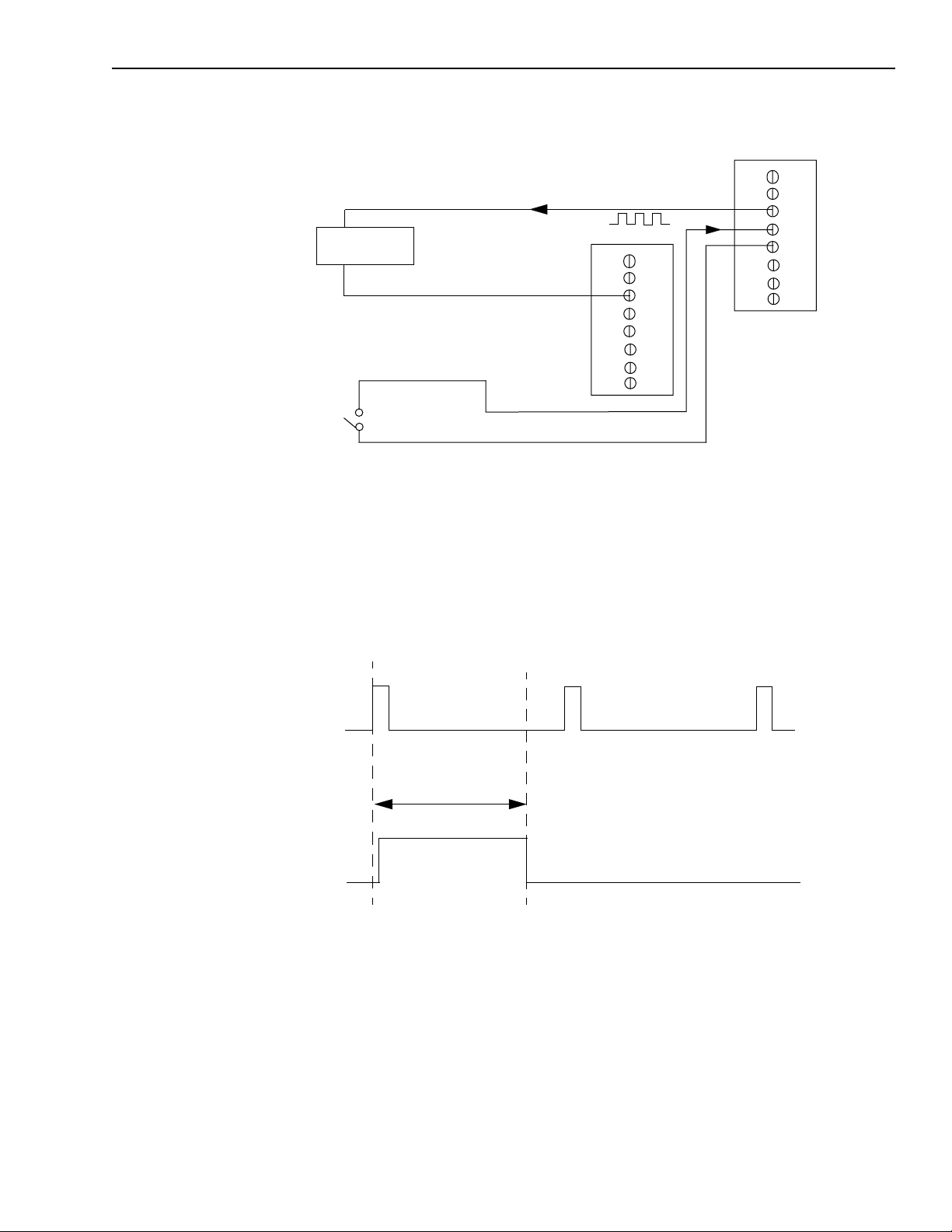
KPCI-3110 and KPCI-3116 User’s Manual Functional Description 2-33
Figure 2-19
Connecting one-shot signals (shown for Counter Output 0 and Gate 0)
Heater
Controller
External
Gating
Switch
Digital Ground
User Counter Output 0
TB83
STP-3110 Screw
Terminal Panel
Gate 0
Digital Ground
TB59
TB60
TB61
Figure 2-20 shows an example of a one-shot operation using an external gate input (rising edge),
a clock output frequency of 1kHz (pulse period of 1ms), a low-to-high pulse type, and a duty
cycle of 99.99%. Figure 2-21 shows the same example using a duty cycle of 50%.
Figure 2-20
Example of one-shot mode using a 99.99% duty cycle
One-Shot Operation Starts
External
Gate
Signal
Pulse
Output
Signal
1ms period
99.99% Duty Cycle
Page 56

2-34 Functional Description KPCI-3110 and KPCI-3116 User’s Manual
Figure 2-21
Example of one-shot mode using a 50% duty cycle
One-Shot Operation Starts
External
Gate
Signal
1ms period
Pulse
Output
Signal
50% Duty Cycle
Repetitive one-shot
Use repetitive one-shot mode to generate a pulse output signal each time the board detects a trigger (determined by the gate input signal). You can use this mode to clean up a poor clock input
signal by changing its pulse width, then outputting it.
In repetitive one-shot mode, the internal C/T clock source is more useful than an external C/T
clock source. Refer to page 2-23 for more information on the internal C/T clock source.
Use DriverLINX software to specify the counter/timer mode as repetitive one-shot, the polarity
of the output pulses (high-to-low transitions or low-to-high transitions), the duty cycle of the
output pulses, the C/T clock source, and the gate type to trigger the operation. Refer to
page 2-25 for more information on pulse output types and to page 2-24 for more information on
gates.
In the case of a one-shot operation, use a duty cycle as close to 100% as possible to output a
pulse immediately. Using a duty cycle closer to 0% acts as a pulse output delay.
When the one-shot operation is triggered (determined by the gate input signal), a pulse is output.
When the board detects the next trigger, another pulse is output. This operation continues until
you stop the operation.
NOTE Triggers that occur while the pulse is being output are not detected by
the board.
Figure 2-22 shows an example of a repetitive one-shot operation using an external gate (rising
edge); a clock output frequency of 1kHz (one pulse every 1ms), a low-to-high pulse type, and a
duty cycle of 99.99%. Figure 2-23 shows the same example using a duty cycle of 50%.
Page 57

KPCI-3110 and KPCI-3116 User’s Manual Functional Description 2-35
Figure 2-22
Example of repetitive one-shot mode using a 99.99% duty cycle
Repetitive One-Shot
Operation Starts
External
Gate
Signal
1ms period
99.99% Duty Cycle
Pulse
Output
Signal
1ms period
99.99% Duty Cycle
Figure 2-23
Example of repetitive one-shot mode using a 50% duty cycle
Repetitive One-Shot
Operation Starts
External
Gate
Signal
1ms period
Pulse
Output
Signal
50% Duty
Cycle
99.99% Duty Cycle
1ms period
50% Duty
Cycle
Page 58

2-36 Functional Description KPCI-3110 and KPCI-3116 User’s Manual
Synchronizing A/D and D/A subsystems
You can synchronize the operation of the A/D and D/A subsystems providing that they are not
performing single value operations. Refer to page 2-7 and page 2-19 for more information on
single value operations.
You can synchronize the A/D and D/A subsystems in two ways: by applying the same external
trigger or by applying the same external clock. This section describes these two methods.
Synchronizing the triggers
You can synchronize the triggers of the A/D and D/A subsystems as follows:
• External digital (TTL) trigger — Using software, specify the trigger source for the A/D
and D/A subsystems as the external digital (TTL) trigger and specify start type as digital trigger. Then, wire an external digital TTL trigger to both the A/D subsystem and the D/A subsystem. When armed, both subsystems are triggered simultaneously when the external
digital event occurs.
Synchronizing the clocks
You can synchronize the clocks of the A/D and D/A subsystems as follows:
• External Sample Clocks — Using software, specify the clock source as the external A/D
sample clock for the A/D subsystem and as the external D/A output clock for the D/A subsystem. When started, both subsystems are clocked simultaneously.
Page 59

3
Installation and
Configuration
Page 60

•
•
•
•
3-2 Installation and Configuration KPCI-3110 and KPCI-3116 User’s Manual
Unpacking
Open the shipping box and remove the wrapped KPCI-3110 or KPCI-3116 board.
CAUTION Keep the board in its protective antistatic bag until you are ready to
install it; this minimizes the likelihood of electro-static damage.
Verify that the following items are present:
KPCI-3110, or KPCI-3116 data acquisition board
KPCI-3110 and KPCI-3116 DriverLINX Software and Documentation CD-ROM
If an item is missing or damaged, call Keithley at:
1-888-KEITHLEY
Monday - Friday, 8:00 a.m. - 5:00 p.m., Eastern Time
An application engineer will guide you through the appropriate steps for replacing missing or
damaged items.
Installing the software
NOTE
Software options
Users of KPCI-3110 and KPCI-3116 boards have the following two software options. In both
cases, the software interfaces with your system via the DriverLINX software provided with your
board:
The user can run a fully integrated data-acquisition software package such as TestPoint or
LabVIEW.
The user can write and run a custom program in Visual C/C++, Visual Basic, or Delphi,
using the programming support provided in the DriverLINX software.
A summary of the pros and cons of using integrated packages or writing custom programs is
provided in the Keithley Full Line Catalog.
The KPCI-3110 or KPCI-3116 board has fully functional driver support for use under
Windows 95/98/NT/2000.
NOTE
Install the DriverLINX software before installing the KPCI-3110 or
KPCI-3116 board. Otherwise, the device drivers will be more difficult to
install.
The DriverLINX Installation and Configuration Guide, explains the
DriverLINX installation process. To display this manual from your
DriverLINX KPCI-3110 and KPCI-3116 CD-ROM, open the Windows
Explorer, then double click on X:\Drvlinx4\Docs\Instconf.pdf, where X =
the letter of the CD-ROM drive. Acrobat Reader must already be
installed on the other system. If necessary, you can first install Acrobat
Reader directly from the CD-ROM by double clicking
X:\Acrobat\setup.exe.
Page 61

•
•
•
•
•
•
•
•
•
•
KPCI-3110 and KPCI-3116 User’s Manual Installation and Configuration 3-3
DriverLINX driver software for Windows 95/98/NT/2000
DriverLINX software, supplied by Keithley with the KPCI-3110 or KPCI-3116 board, provides
convenient interfaces to configure analog and digital I/O modes without register-level
programming.
Most importantly, however, DriverLINX supports those programmers who wish to create custom applications using Visual C/C++, Visual Basic, or Delphi. DriverLINX accomplishes foreground and background tasks to perform data acquisition. The software includes memory and
data buffer management, event triggering, extensive error checking, and context sensitive online help.
DriverLINX provides application developers a standardized interface to over 100 services for
creating foreground and background tasks for the following:
Analog input and output
Digital input and output
Time and frequency measurement
Event counting
Pulse output
Period measurement
In addition to basic I/O support, DriverLINX also provides:
Built-in capabilities to handle memory and data buffer management.
A selection of starting and stopping trigger events, including pre-triggering, mid-point trig-
gering and post-triggering protocols.
Extensive error checking.
Context-sensitive on-line help system DriverLINX is essentially hardware independent,
because its portable APIs (Application Programming Interfaces) work across various operating systems. This capability eliminates unnecessary programming when changing operating
system platforms.
TestPoint
TestPoint is a fully featured, integrated application package that incorporates many commonly
used math, analysis, report generation, and graphics functions. The TestPoint graphical dragand-drop interface can be used to create data acquisition applications, without programming, for
IEEE-488 instruments, data acquisition boards, and RS232-485 instruments and devices.
TestPoint includes features for controlling external devices, responding to events, processing
data, creating report files, and exchanging information with other Windows programs. It provides libraries for controlling most popular GPIB instruments.
TestPoint interfaces with your KPCI-3110 or KPCI-3116 board through DriverLINX, using a
driver that is provided by the manufacturer.
™
Page 62

™
3-4 Installation and Configuration KPCI-3110 and KPCI-3116 User’s Manual
LabVIEW
LabVIEW is a fully featured graphical programming language used to create virtual instrumentation. It consists of an interactive user interface, complete with knobs, slide switches, graphs,
strip charts, and other instrument panel controls. Its data-driven environment uses function
blocks that are virtually wired together and pass data to each other. The function blocks, which
are selected from palette menus, range from arithmetic functions to advanced acquisition, control, and analysis routines. Also included are debugging tools, help windows, execution highlighting, single stepping, probes, and breakpoints to trace and monitor the data flow execution.
LabVIEW can be used to create professional applications with minimal programming.
A Keithley VI palette provides standard virtual instruments (VIs) for LabVIEW that interface
with your KPCI-3110 or KPCI-3116 board through DriverLINX. The needed driver is provided
on your DriverLINX CD-ROM or may be obtained by download at www.keithley.com.
Installing DriverLINX
Refer to the instructions on the Read this first sheet and the manuals on the DriverLINX
CD-ROM, both shipped with your board, for information on installing and using DriverLINX.
Installing application software and drivers
Installing the TestPoint software and driver
The DriverLINX driver for TestPoint is provided as part of the TestPoint software. The driver
therefore installs automatically when you install TestPoint.
You can install TestPoint application software at any time—before or after installing DriverLINX and the KPCI-3110 or KPCI-3116 board. For TestPoint installation instructions, consult
the manual provided by with TestPoint.
NOTE
Installing the LabVIEW software and driver
A DriverLINX driver for LabVIEW is provided on your DriverLINX CD-ROM. The LabVIEW
driver does not install automatically when you install DriverLINX and your board. You must first
install the LabVIEW application program, then install the DriverLINX driver. Access the LabVIEW driver installation routine by starting setup.exe on the DriverLINX CD-ROM, then selecting LabVIEW
Consult the manual provided with LabVIEW for installation instructions.
Before using TestPoint with the KPCI-3110 version of DriverLINX,
check with Keithley to ensure that your version of TestPoint is compatible with DriverLINX.
™
Support from the Install These DriverLINX components screen.
Page 63

•
•
•
•
KPCI-3110 and KPCI-3116 User’s Manual Installation and Configuration 3-5
Installing the board
To install the board, check the system requirements, set up the computer, select an available
32-bit or 64-bit PCI expansion slot, and insert the board into the slot. The following subsections
describe how to perform these steps.
To install the board, perform the following steps:
Check the system requirements, described in Section 1, “Overview.”
Set up the computer, described on page 3-5.
Select an expansion slot, described on page 3-5.
Insert the board into any available 32-bit or 64-bit PCI expansion slot in your computer,
described on page 3-6.
NOTE
The KPCI-3110 and KPCI-3116 boards are factory-calibrated and
require no further adjustment prior to installation. If you decide later to
recalibrate the board, refer to Section 5 , “ Calibration ,” for instructions.
Setting up the computer
CAUTION To prevent electro-static damage that can occur when handling elec-
tronic equipment, use a ground strap or similar device when performing this installation procedure.
1. Turn off the computer.
2. Turn off all peripherals (printer, modem, monitor, and so on) connected to the computer.
3. Unplug the computer and all peripherals.
4. Remove the cover from you computer. Refer to your computer’s user manual for
instructions.
Selecting an expansion slot
1. Select a 32-bit or 64-bit PCI expansion slot.
PCI slots are shorter than ISA or EISA slots and are usually white or ivory. Commonly, three
PCI slots (one of which may be a shared ISA/PCI slot) are available. If an ISA board exists
in the shared slot, you cannot use the slot for a PCI board; likewise if a PCI board exists in
the shared slot, you cannot use the slot for an ISA board.
2. Remove the cover plate from the selected expansion slot. Retain the screw that held it in
place; you will use it later to install the board.
Page 64

3-6 Installation and Configuration KPCI-3110 and KPCI-3116 User’s Manual
Inserting the board in the computer
1. To discharge any static electricity, hold the wrapped board in one hand while placing your
other hand firmly on a metal portion of the computer chassis.
2. Carefully remove the anti-static packing material from the board. (Save the original packing
material in the unlikely event that your board requires servicing in the future.)
3. Hold the board by its edges and do not touch any of the components on the board.
4. Position the board so that the cable connectors are facing the rear of the computer, as shown
in Figure 3-1.
Figure 3-1
Inserting a KPCI-3110 or KPCI-3116 board in the computer
KPCI-3110 or
KPCI-3116 Board
PCI Expansion Slot Bus Connector
Rear of Computer
5. Carefully lower the board into the PCI expansion slot using the card guide to properly align
the board in the slot. When the bottom of the board contacts the bus connector, gently press
down on the board until it clicks into place.
CAUTION
Do not force the board into place. Moving the board from side to side during
installation may damage the bus connector. If you encounter resistance
when inserting the board, remove the board and try again.
6. Secure the board in place at the rear panel of the system unit using the screw removed from
the slot cover.
Page 65

KPCI-3110 and KPCI-3116 User’s Manual Installation and Configuration 3-7
Configuring the board to work with DriverLINX
After physically installing the board, turn on and reboot the computer. The DriverLINX Plug
and Play Wizard screen appears. Run the Wizard immediately by following the progressive
instructions on the screen.
If you do not run the Wizard immediately, it will not appear the next time you reboot. You must
then restart the Wizard from a batch file, as follows:
1. Open the Windows Explorer.
2. Double click on X:\DrvLINX4\Help\kcpi3110.bat, where X = the letter of the drive on
which you installed DriverLINX.
3. The Wizard appears.
NOTE
You can also start this batch file directly from the CD-ROM by double
clicking on Y:\DrvLINX4\Help\kpci3110.bat, where Y = the drive letter
of your CD-ROM drive.
Checking the combined board and DriverLINX installations
Before making any connections to the board, check whether DriverLINX and your board are
installed correctly and working together properly. Refer to Section 4, “Testing the Board” and
the DriverLINX manuals.
Try starting the DriverLINX Analog I/O Panel. Proceed as follows:
1. In the Start menu, click Programs.
2. Find the DriverLINX → Test Panels folder, under which you should find the AIO Panel
entry.
3. Click on the AIO Panel entry.
4. If a KPCI-3110 or KPCI-3116 board is the only board in your computer installed under
DriverLINX or if the DriverLINX Analog I/O Panel lists the KPCI3110 board under Driver
Selection, then DriverLINX and your board are installed properly and are working together.
5. If you cannot initially run the Analog I/O Panel, refer to Section 6, “Troubleshooting.”
After DriverLINX and your board are installed properly and working together, continue with
installation and wiring.
Page 66
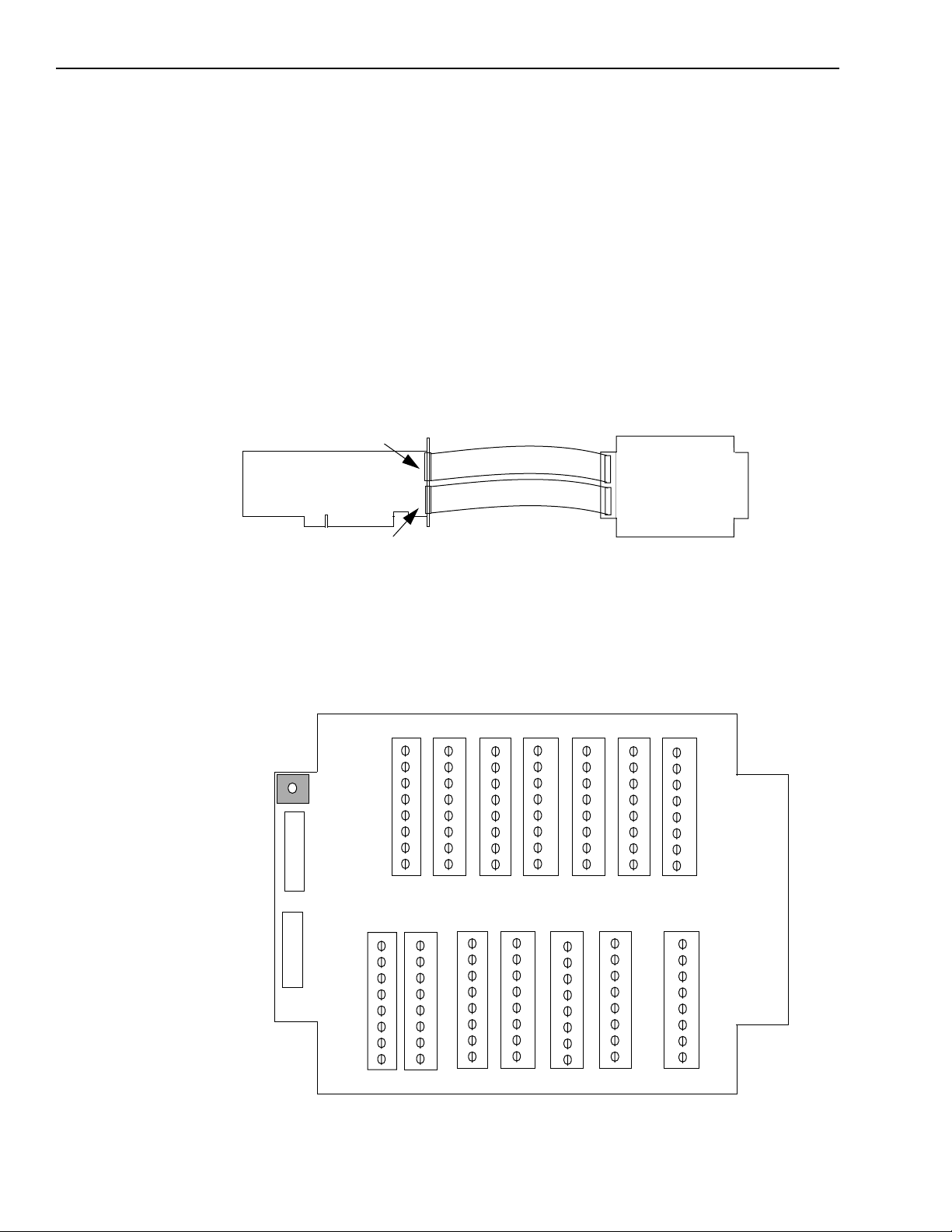
3-8 Installation and Configuration KPCI-3110 and KPCI-3116 User’s Manual
Attaching the STP-3110 screw terminal panel
Before you can wire signals, you first need to attach the STP-3110 screw terminal panel to the
KPCI-3110 or KPCI-3116 board. Connector J1 on the screw terminal panel brings out all of the
analog signals from connector J1 on the KPCI-3110 or KPCI-3116 board; cable CAB-307 connects connector J1 on the screw terminal panel to the KPCI-3110 or KPCI-3116 board. Connector J2 on the screw terminal panel brings out all of the digital and counter/timer signals from
connector J2 on the KPCI-3110 or KPCI-3116 board; cable CAB-308 connects connector J2 on
the screw terminal panel to the KPCI-3110 or KPCI-3116 board.
Figure 3-2 illustrates how to attach the STP-3110 screw terminal panel to the KPCI-3110 or
KPCI-3116 board.
Figure 3-2
Attaching the STP-3110 screw terminal panel to the KPCI-3110 or KPCI-3116 board
Analog I/O
Connector (J1)
KPCI-3110 or
KPCI-3116 Board
CAB-307 Cable
CAB-308 Cable
J1
STP-3110 Screw
Terminal Panel
J2
Digital I/O
Connector (J2)
Figure 3-3 shows the layout of the STP-3110 screw terminal panel.
Figure 3-3
Layout of the STP-3110 screw terminal panel
1
W1
R1 to R16
J1
J2
R17 to R32
Gnd 0
Clk 0
Out 0
Gate 0
Gnd 1
Clk 1
Out 1
Gate 1
CTR
57
64
8
CTR
65
72
9
16
Trig
73
80
17
24
GND
81
88
25
32
DIO
89
96
33
40
41
48
DIO
97
104
49
56
Shield
105
112
Page 67

KPCI-3110 and KPCI-3116 User’s Manual Installation and Configuration 3-9
Size
The STP-3110 panel is designed to fit inside a standard 4-inch wide by 8-inch long plastic enclosure. Note, that the grayed area on the STP-3110, shown in Figure 3-3, indicates where to connect a single ground point for shielded enclosures.
Jumper W1 - common ground sense
When shipped from the factory, jumper W1 connects the low side of the input amplifier (Amp
Low) on the KPCI-3110 or KPCI-3116 board to analog ground.
When using pseudo-differential analog inputs, remove jumper W1 and connect Amp Low to a
remote common-mode voltage to reject offset voltages common to all 32 input channels. Refer
to Figure 3-4 for an example of using jumper W1.
Figure 3-4
Removal of Jumper W1 for remote ground sensing
Signal Source
Vsource 0
Vsource 8
Vsource 1
Signal Source
Vsource 0
Vsource 8
Vsource 1
STP-3110 Panel
+
Analog In 0
Analog In 8
+
+
Analog In 1
+
+
+
Analog Ground
Analog In 0
Analog In 8
Analog In 1
TB1
TB2
TB3
TB1
TB2
TB3
Jumper W1 Installed
(Amp Low)
TB33
TB34
TB33
TB34
W1
STP-3110
Panel
*
V
CM
Remove Jumper W1 to use Amp Low
as a remote ground sense.
Analog Ground
*Make this connection as close to V
Vcm is the common-mode voltage for all 32 analog inputs.
as possible to reduce ground loop errors.
sources
Page 68

3-10 Installation and Configuration KPCI-3110 and KPCI-3116 User’s Manual
Resistors R1 to R16 - bias return
Resistor locations R1 to R16 connect the low side of analog input channels to analog ground.
These resistor locations are typically used when connecting differential inputs to analog input
channels 0 to 15, where R1 corresponds to analog input channel 0, and R16 corresponds to analog input channel 15.
The high side of the corresponding analog input channels returns the source input impedance
through the bias return resistors to the low side of the channels, then to analog ground. Typical
resistor values are 1k Ω to 100k Ω depending on the application. Refer to Figure 3-7 for an example of using bias return resistors.
Resistors R17 to R32 - current shunt
Resistor locations R17 to R32 are typically used to convert current to voltage on channels 0 to
15, where R17 corresponds to analog input channel 0, and R32 corresponds to analog input
channel 15.
These resistor locations connect the high side to the low side of the corresponding channels,
thereby acting as shunts. If, for example, you add a 250 Ω resistor to location R17, and connect a
4 to 20mA current loop input to channel 0, the input range is converted to 1 to 5V. Note that,
depending on your application, you may need to use resistors R1 to R16 with resistors R17 to
R32 for proper operation. Refer to Figure 3-9 for an example of using current shunt resistors.
Screw terminals
Screw terminals TB1 to TB56 correspond to the analog I/O channels from the KPCI-3110 or
KPCI-3116 board. Screw terminals TB57 to TB112 correspond to the digital I/O signals from
the KPCI-3110 or KPCI-3116 board.
Screw terminals TB37 (+15V) and TB39 ( − 15V) are available for low-current signal conditioning applications. The supply on the KPCI-3110 or KPCI-3116 board is current-limited through a
10 Ω resistor and is specified for a maximum load current of ±3mA.
Screw terminal TB49 (+5.0V reference) is also current-limited through a 10 Ω resistor and is
provided for applications that require a reference less than 1mA.
Screw terminal TB112 (+5V output) is current-limited through a series 10 Ω resistor and supports loads up to 100mA. Note that you must take the drop (current [I] multiplied by resistance
[R]) across the series 10 Ω resistor (1V at 100mA) into consideration.
To provide maximum signal integrity, screw terminals TB35, TB36, and TB51 to TB56 have
been reserved for external shield connections from the J1 connector. Screw terminals TB105 and
TB108 have been reserved for external shield connections from the J2 connector. In addition,
multiple ground connections have been allocated for all the digital and clock signals for proper
shielding and current capacity.
NOTE
If you connect a high-speed clock to the STP-3110, it is recommended
that you connect the return to the adjacent ground screw terminal.
Page 69

−
KPCI-3110 and KPCI-3116 User’s Manual Installation and Configuration 3-11
Table 3-1 lists the screw terminal assignments for connector J1 on the STP-3110 screw terminal
panel. Table 3-2 lists the screw terminal assignments for connector J2 on the STP-3110 screw
terminal panel.
Table 3-1
Screw terminal assignments for connector J1on the STP-3110 screw terminal panel
TB # J1 Pin # Description TB # J1 Pin # Description
1 25 Analog In 0/0 2 50 Analog In 8/0 Return
3 24 Analog In 1/1 4 49 Analog In 9/1 Return
5 23 Analog In 2/2 6 48 Analog In 10/2 Return
7 22 Analog In 3/3 8 47 Analog In 11/3 Return
9 21 Analog In 4/4 10 46 Analog In 12/4 Return
11 20 Analog In 5/5 12 45 Analog In 13/5 Return
13 19 Analog In 6/6 14 44 Analog In 14/6 Return
15 18 Analog In 7/7 16 43 Analog In 15/7 Return
17 17 Analog In 16/8 18 42 Analog In 24/8 Return
19 16 Analog In 17/9 20 41 Analog In 25/9 Return
21 15 Analog In 18/10 22 40 Analog In 26/10 Return
23 14 Analog In 19/11 24 39 Analog In 27/11 Return
25 13 Analog In 20/12 26 38 Analog In 28/12 Return
27 12 Analog In 21/13 28 37 Analog In 29/13 Return
29 11 Analog In 22/14 30 36 Analog In 30/14 Return
31 10 Analog In 23/15 32 35 Analog In 31/15 Return
33 9 Amp Low 34 34 Analog Ground
35 8 Analog Shield Ground 36 33 Analog Shield Ground
37 7 +15V Output 38 32 Power Ground
39 6
41 5 Analog Output 0+ 42 30 Analog Output 0 Return
43 4 Analog Output 1+ 44 29 Analog Output 1 Return
45 3 Reserved 46 28 Reserved
47 2 Reserved 48 27 Reserved
49 1 +5V Reference Out 50 26 Analog Ground
51 - Analog Shield Ground 52 - Analog Shield Ground
53 - Analog Shield Ground 54 - Analog Shield Ground
55 - Analog Shield Ground 56 - Analog Shield Ground
15V Output 40 31 Reserved
NOTE
For analog input channels (TB1-32), two values are shown. The value
before the slash is the assignment in single-ended and pseudo-differential
configurations when 32 channels are available. The value after the slash
applies to differential configurations, when 16 channels are available
and each channel has a separate return.
In particular, be aware that when changing to/from differential configuration, the high side of channels 8-15 must be moved to a different terminal.
Page 70

3-12 Installation and Configuration KPCI-3110 and KPCI-3116 User’s Manual
Table 3-2
Screw terminal assignments for connector J2 on the STP-3110 screw terminal panel
TB # J2 Pin # Description TB # J2 Pin # Description
57 51, 52 Digital Ground 58 17 User Clock Input 0
59 16 User Counter Output 0 60 50 External Gate 0
61 49 Digital Ground 62 15 User Clock Input 1
63 14 User Counter Output 1 64 48 External Gate 1
65 47 Digital Ground 66 13 User Clock Input 2
67 12 User Counter Output 2 68 46 External Gate 2
69 45 Digital Ground 70 11 User Clock Input 3
71 10 User Counter Output 3 72 44 External Gate 3
73 43 Digital Ground 74 9 External D/A Sample
Clock In
75 8 External D/A TTL Trigger 76 7 External A/D Sample
Clock In
77 6 External A/D TTL Trigger 78 5 A/D Trigger Out
79 4 A/D Sample Clock Out 80 3 Reserved
81 23, 28, 42Digital Ground 82 39, 41,
57, 62
83 18, 38,
40, 63,
64
85 31 Reserved 86 37 Reserved
87 30 Dynamic Digital Output 0 88 29 Dynamic Digital Output 1
89 27 Digital I/O Bank A 0 90 26 Digital I/O Bank A 1
91 25 Digital I/O Bank A 2 92 24 Digital I/O Bank A 3
93 61 Digital I/O Bank A 4 94 60 Digital I/O Bank A 5
95 59 Digital I/O Bank A 6 96 58 Digital I/O Bank A 7
97 22 Digital I/O Bank B 0 98 21 Digital I/O Bank B 1
99 20 Digital I/O Bank B 2 100 19 Digital I/O Bank B 3
101 56 Digital I/O Bank B 4 102 55 Digital I/O Bank B 5
103 54 Digital I/O Bank B 6 104 53 Digital I/O Bank B 7
105 33 Digital Shield Ground 106 68 Analog Ground
107 34 Analog Trigger 108 67 Digital Shield Ground
109 32 Reserved 110 66 Reserved
111 35, 36 Digital Ground 112 1, 2 +5V Out
Digital Ground 84 65 Reserved
Digital Ground
Page 71

KPCI-3110 and KPCI-3116 User’s Manual Installation and Configuration 3-13
Wiring signals
This section describes how to wire signals to the STP-3110 screw terminal panel.
CAUTION To avoid electrical damage, ensure that power is turned off to the
computer and to any attached devices before wiring signals to the
STP-3110 screw terminal panel.
•
•
•
•
•
TIP
Keep the following recommendations in mind when wiring signals to the STP-3110 screw terminal panel:
Use individually shielded twisted-pair wire (size 14 to 26 AWG) when using the KPCI-3110
or KPCI-3116 board in high electrical noise environments.
Separate power and signal lines by using physically different wiring paths or conduits.
To avoid noise, do not locate the STP-3110 screw terminal panel and cabling next to sources
that produce high electromagnetic fields, such as large electric motors, power lines, solenoids, and electric arcs, unless the signals are enclosed in a metal shield.
Connect the analog shield to screw terminals TB35 and TB36, and to TB51 through TB56 on
the STP-3110 screw terminal panel.
Connect the digital shield to screw terminals TB105 and TB108 on the screw terminal panel.
• Connect the analog and digital shields to one end only (either at the STP-3110 or at the sig-
nal source).
When first installing the board, try wiring a function generator or a
known voltage source to analog input channel 0 (use the differential
configuration), an oscilloscope or voltage meter to analog output channel 0, a digital input to digital I/O Port A, and an external clock or scope
to counter/timer channel 0. Then, run DriverLINX Analog I/O Panel to
verify that the board is operating properly. Once you have determined
that the board is operating properly, wire the signals according to your
application’s requirements.
Connecting analog input signals
The STP-3110 screw terminal panel supports both voltage and current loop inputs. You can connect analog input voltage signals to the STP-3110 in the following configurations:
• Single-ended — Choose this configuration when you want to measure high-level signals,
noise is not significant, the source of the input is close to the STP-3110 screw terminal panel,
and all the input signals are referred to the same common ground. When you choose the
single-ended configuration, all 32 analog input channels are available.
• Pseudo-Differential — Choose this configuration when noise or common-mode voltage
(the difference between the ground potentials of the signal source and the ground of the
STP-3110 screw terminal panel or between the grounds of other signals) exists and the
differential configuration is not suitable for your application. This option provides less noise
rejection than the differential configuration; however, all 32 analog input channels are
available.
• Differential — Choose this configuration when you want to measure low-level signals (less
than 1V), you are using an A/D converter with high resolution (> 12 bits), noise is a significant part of the signal, or common-mode voltage exists. When you choose the differential
configuration, 16 analog input channels are available.
Page 72

3-14 Installation and Configuration KPCI-3110 and KPCI-3116 User’s Manual
NOTE It is recommended that you connect all unused analog input channels to
analog ground.
This section describes how to connect single-ended, pseudo-differential, and differential voltage
inputs, as well as current loop inputs to the STP-3110 screw terminal panel.
Connecting single-ended voltage inputs
Figure 3-5 shows how to connect single-ended voltage inputs (channels 0, 1, and 8, in this case)
to the STP-3110 screw terminal panel.
Figure 3-5
Connecting single-ended voltage inputs (shown for Channels 0, 1, and 8)
Signal Source
-
Vsource 0
-
Vsource 8
Vsource 1
STP-3110 Panel
+
Analog In 0
Analog In 8
+
+
Analog In 1
TB1
TB2
TB3
Analog Ground
Jumper W1 Installed
(Amp Low)
TB33
TB34
W1
Page 73

KPCI-3110 and KPCI-3116 User’s Manual Installation and Configuration 3-15
Connecting pseudo-differential voltage inputs
Figure 3-6 shows how to connect pseudo-differential voltage inputs (channels 0, 1, and 8, in this
case) to the STP-3110 screw terminal panel.
Figure 3-6
Connecting pseudo-differential voltage inputs (shown for Channels 0, 1, and 8)
Signal Source
Vsource 0
Vsource 8
Vsource 1
*
V
CM
+
Analog In 0
Analog In 8
+
+
Remove Jumper W1 to use Amp Low as a
remote ground sense.
Analog In 1
Analog Ground
*Make this connection as close to V
ground loop errors. Vcm is the common-mode voltage for all 32
analog inputs.
TB1
TB2
TB3
TB33
TB34
STP-3110
Panel
as possible to reduce
sources
Page 74

3-16 Installation and Configuration KPCI-3110 and KPCI-3116 User’s Manual
Connecting differential voltage inputs
Figure 3-7A illustrates how to connect a floating signal source to the STP-3110 screw terminal
panel using differential inputs. (A floating signal source is a voltage source that has no connection with earth ground.) For floating signal sources, you need to provide a bias return path by
adding resistors R1 to R16 for channels 0 to 15, respectively.
If the input signal is +10V, then the common-mode voltage could be 1V. Theoretically, the resistor value (Rb) should be 1V divided by the input bias current (20nA) or 50mΩ. However, when
you add noise from external sources to the high impedance, a resistor value of 100Ω to 100kΩ is
more practical.
In Figure 3-7B, the signal source itself provides the bias return path; therefore, you do not need
to use bias return resistors. Rs is the signal source resistance while Rv is the resistance required
to balance the bridge. Note that the negative side of the bridge supply must be returned to analog
ground.
Figure 3-7
Connecting differential voltage inputs (shown for Channel 0)
A)
Floating
Signal
Source
B)
R
v
R
+
R
s
s
DC Supply
Bridge
+
-
-
Analog In 0
Analog In 0
Return
Analog In 0
Analog In 0
Return
R1
Analog Ground
Analog Ground
TB1
TB2
TB2
TB1
TB34
STP-3110
Panel
You can use resistor R1 to
connect the low side of
channel 0 to analog ground.
TB34
STP-3110
Panel
Page 75

KPCI-3110 and KPCI-3116 User’s Manual Installation and Configuration 3-17
Note that since they measure the difference between the signals at the high (+) and low (−)
inputs, differential connections usually cancel any common-mode voltages, leaving only the signal. However, if you are using a grounded signal source and ground loop problems arise, connect
the differential signals to the STP-3110 screw terminal panel as shown in Figure 3-8. In this
case, make sure that the low side of the signal (−) is connected to ground at the signal source, not
at the STP-3110 screw terminal panel, and do not tie the two grounds together.
Figure 3-8
Connecting differential voltage inputs from a grounded signal source
(shown for Channel 0)
STP-3110 Panel
TB1
TB2
TB34
Grounded
Signal
Source
E
s
Signal Source
Ground V
g1
+
-
Analog In 0
Analog In 0
Return
R1
Analog Ground
Resistor R1 should be installed for bias return in
case the external ground is floating.
Connecting current loop inputs
Figure 3-9 shows how to connect a current loop input (channel 0, in this case) to the STP-3110
screw terminal panel.
Figure 3-9
Connecting current inputs to the STP-3110 screw terminal panel (shown for Channel 0)
+V
CC
4 to 20mA
Analog Input 0
+
-
TB1
R17
TB2
STP-3110 Panel
TB50
TB51
Analog Input 0
Return
R1
Analog Ground
Analog Shield
Use current shunt resistor R17 to convert current to voltage; 250Ω for 4 to
20mA = 1 to 5V. The common side of the external loop supply must either
connect to analog ground or, if needed, to a bias return resistor (R1 in this case)
Page 76

3-18 Installation and Configuration KPCI-3110 and KPCI-3116 User’s Manual
Connecting analog output signals
Figure 3-10 shows how to connect analog output voltage signals (channel 0, in this case) to the
STP-3110 screw terminal panel.
Figure 3-10
Connecting analog output voltages to the STP-3110 screw terminal panel
(shown for Channel 0)
Load
Connecting digital I/O signals
Figure 3-11 shows how to connect a digital input signal (lines 0 and 1 of digital Bank A, in this
case) to the STP-3110 screw terminal panel.
Figure 3-11
Connecting digital inputs to the STP-3110 screw terminal panel
(Lines 0 and 1, Bank A shown)
TTL Inputs
Analog Output 0
Analog Output 0
Return
Analog Shield
TB41
TB42
Digital I/O Bank A 0
Digital I/O Bank A 1
TB51
STP-3110
Panel
TB89
TB90
Digital Shield
TB105
STP-3110 Panel
Page 77

KPCI-3110 and KPCI-3116 User’s Manual Installation and Configuration 3-19
Figure 3-12 shows how to connect a digital output signal (line 0 of digital Bank B, in this case)
to the STP-3110 screw terminal panel.
Figure 3-12
Connecting digital outputs to the STP-3110 screw terminal panel (Line 0, Bank B shown)
0 Out = LED On
TB97
5V
+
-
500Ω
Digital Ground
Digital I/O Bank B 0
TB81
STP-3110 Panel
Connecting counter/timer signals
The KPCI-3110 or KPCI-3116 boards with the STP-3110 screw terminal panel provide user
counter/timers that you can use to perform the following operations:
• Event counting
• Frequency measurement
• Pulse output (rate generation, one-shot, and repetitive one-shot)
This section describes how to connect counter/timer signals to perform these operations. Refer
to Section 2, “Functional Description,” for more information on using the counter/timers.
Page 78
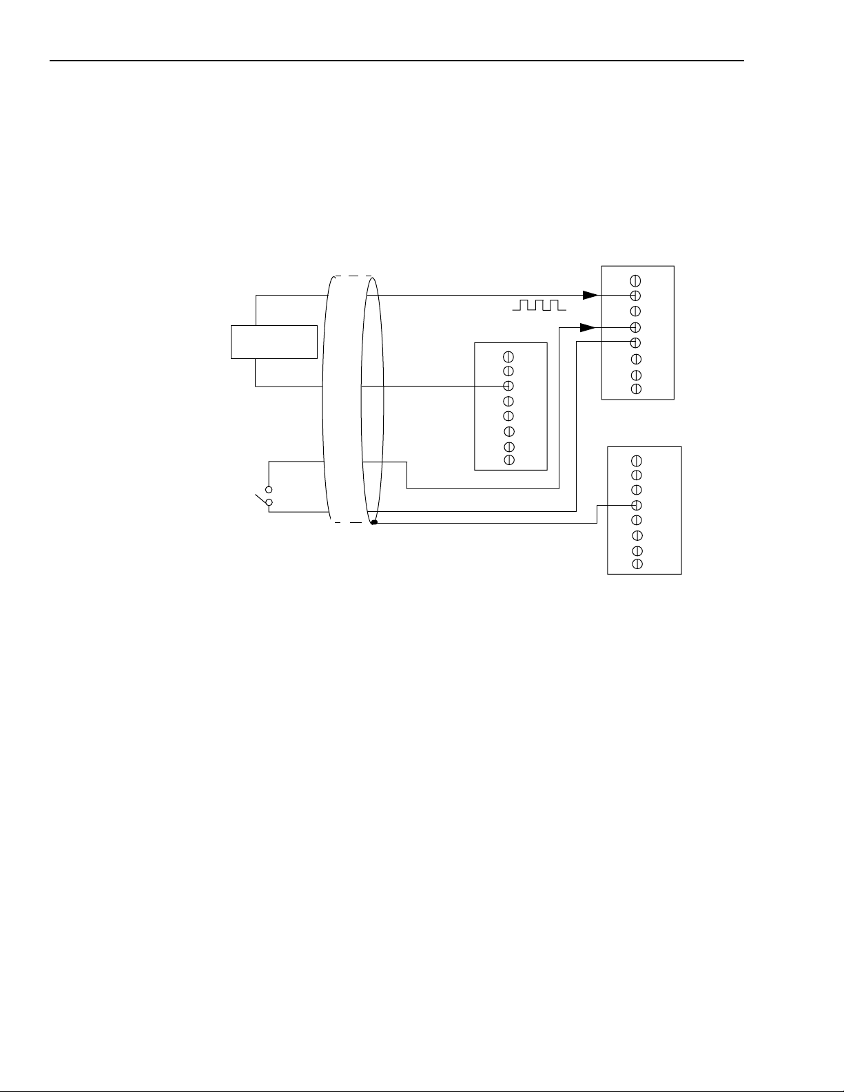
3-20 Installation and Configuration KPCI-3110 and KPCI-3116 User’s Manual
Connecting event counting signals
Figure 3-13 shows one example of connecting event counting signals to the STP-3110 screw ter-
minal panel using user counter 0. In this example, rising clock edges are counted while the gate
is active.
Figure 3-13
Connecting event counting applications to the STP-3110 screw terminal panel
(shown for Clock Input 0 and External Gate 0)
Signal Source
External
Gating
Switch
Digital Ground
User Clock Input 0
TB83
Gate 0
Digital Ground
Digital Shield
TB58
TB60
TB61
STP-3110 Panel
TB108
Page 79

KPCI-3110 and KPCI-3116 User’s Manual Installation and Configuration 3-21
Figure 3-14 shows another example of connecting an event counting application to the
STP-3110 screw terminal panel using user counter 0. In this example, a software gate is used to
start the event counting operation.
Figure 3-14
Connecting event counting applications to the STP-3110 screw terminal panel without
an external gate input (shown for Clock Input 0)
Signal Source
Digital Ground
User Clock Input 0
TB83
Digital Shield
TB58
TB60
TB61
STP-3110 Panel
TB108
Page 80

3-22 Installation and Configuration KPCI-3110 and KPCI-3116 User’s Manual
Figure 3-15 shows an example of how to externally cascade two counters to perform an event
counting operation using user counters 0 and 1. Note that you can also internally cascade
counters using software; if you internally cascade the counters, you do not have to make the
external cascading connections. Note also that this example shows the use of an external gate;
however, this connection is not required.
Figure 3-15
Cascading counters (shown for event counting using Counters 0 and 1
and External Gate 0)
User
Signal Source
Digital Ground
User Clock Input 0
Gate 0
Gate 1
TB83
TB58
TB59
TB60
TB61
TB62
TB64
Counter
Output 0
User Clock
Input 1
External
Gating
Switch
STP-3110 Panel
Digital Ground
TB108
Digital Shield
Page 81
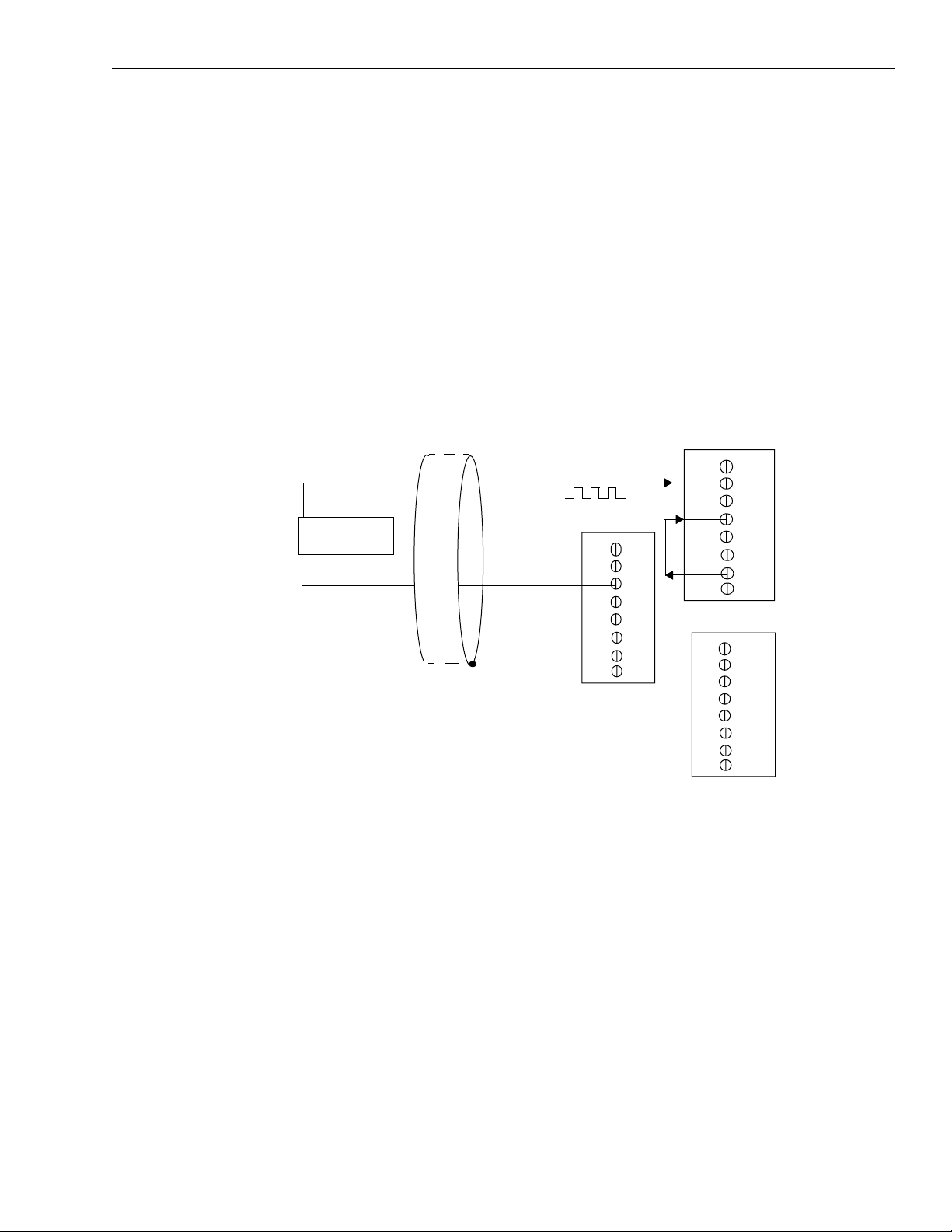
KPCI-3110 and KPCI-3116 User’s Manual Installation and Configuration 3-23
Connecting frequency measurement signals
You can connect a frequency measurement application to the STP-3110 screw terminal panel in
two ways.
The first configuration uses the same wiring as an event counting application that does not use an
external gate signal (see Figure 3-14) the software uses the Windows timer to specify the duration of the frequency measurement. In this configuration, the frequency of the clock input is the
number of counts divided by the duration of the Windows timer.
If you need more accuracy than the Windows timer provides, you can connect a pulse of a
known duration (such as a one-shot output of another user counter) to the external gate input, as
shown in Figure 3-16. In this configuration, the frequency of the clock input is the number of
counts divided by the period of the external gate input.
Figure 3-16
Connecting frequency measurement applications to the STP-3110 screw terminal panel
(shown for Clock Input 0 and External Gate 0)
Signal Source
Digital Ground
Digital Shield
User Clock Input 0
Gate 0
TB83
TB58
TB60
TB61
TB63
STP-3110 Panel
TB108
User Counter
Output 1
Page 82

3-24 Installation and Configuration KPCI-3110 and KPCI-3116 User’s Manual
Connecting pulse output signals
Figure 3-17 shows one example of connecting a pulse output application to the STP-3110 screw
terminal panel using user counter 0. Other combinations of signals can be used.
Figure 3-17
Connecting pulse output applications to the STP-3110 screw terminal panel (shown for
Counter Output 0 and Gate 0)
External
Gating
Switch
Heater
Controller
User Counter Output 0
Digital Ground
TB83
Gate 0
Digital Ground
Digital Shield
TB59
TB60
TB61
STP-3110 Panel
TB108
Figure 3-18 shows an example of how to externally cascade two counters to perform a rate gen-
eration operation using user counters 0 and 1. Note that you can also internally cascade counters
using software; if you internally cascade the counters, you do not have to make the external cascading connections. In this example, counter 1 gate is logic high.
Page 83

KPCI-3110 and KPCI-3116 User’s Manual Installation and Configuration 3-25
Figure 3-18
Cascading counters (shown for rate generation using Counters 0 and 1
and External Gate 0)
User
Counter
Output 0
User Clock
Input 1
Signal Source
External
Gating
Switch
Digital Ground
User Clock Input 0
Gate 0
Digital Ground
Digital Shield
TB57
TB58
TB59
TB60
TB61
TB62
STP-3110 Panel
TB108
Figure 3-19 shows an example of how to externally cascade two counters to perform a one-shot
operation using user counters 0 and 1. Note that you can also internally cascade counters using
software; if you internally cascade the counters, you do not have to make the external cascading
connections. In this example, counter 0 gate is logic high.
Figure 3-19
Cascading counters (shown for one-shot using Counters 0 and 1 and External Gate 1)
Signal Source
One-Shot
Trigger
Digital Ground
User Clock Input 0
Digital Ground
Gate 1
Digital Shield
TB57
TB58
TB64
STP-3110 Panel
TB108
TB59
TB61
TB62
User
Counter
Output 0
User Clock
Input 1
Page 84

4
Testing the Board
Page 85

4-2 Testing the Board KPCI-3110 and KPCI-3116 User’s Manual
The test panels are small applications programs within DriverLINX that allow you to perform
limited data acquisition functions. You can use the panels to do tasks such as:
• Monitor one or two analog input channels on-screen.
• Set the levels of one or two analog output channels.
• Monitor and set digital input and output bits.
Test panels are designed primarily for testing the functions of your board. However, one panel in
particular—the Analog I/O panel—can be useful for limited routine tasks.
This section describes how to use the DriverLINX Analog I/O Panel and DriverLINX Test Panel
utilities to verify the operation of your KPCI-3110 or KPCI-3116 board.
DriverLINX analog I/O panel
The DriverLINX Analog I/O Panel is an application that demonstrates analog input/output using
DriverLINX. With the Analog I/O Panel you can:
• Analyze analog signals using the two-channel Oscilloscope.
• Measure analog voltages using the Digital Volt Meter.
• Generate Sine, Square and Triangle waves using the SST Signal Generator.
• Output DC Level voltages using the Level Control.
• Set and read all digital input and output bits on your board.
The Analog I/O Panel is useful for:
• Testing the KPCI-3110 or KPCI-3116 board DriverLINX installation and configuration.
• Verifying signal inputs to your KPCI-3110 or KPCI-3116 board.
• Sending test signals to external devices.
• Controlling the DC output voltages of two analog output channels.
• Setting and reading all digital input and output bits on your board.
Start the DriverLINX Analog I/O Panel as follows:
1. In the Start menu, click Programs.
2. Find the DriverLINX → Test Panels folder, under which you should find the AIO Panel
entry.
3. Click on the AIO Panel entry. The Analog I/O Panel setup screen appears.
• If a KPCI-3110 or KPCI-3116 board is the only board in your computer installed under
DriverLINX, only one item appears under Driver Selection.
• If more than one type of board is installed in your computer under DriverLINX, the Ana-
log I/O Panel will list multiple drivers under Driver Selection and multiple devices listed
under Device Selection (for example, Device0, Device1, etc.).Your board type and
device number may not be displayed initially. If so, click the scroll buttons next to the
Driver Selection and Device Selection text boxes until your KPCI-3110 board type and
device number are displayed.
4. Select the Logical Device you want to operate by dragging the pointer in the Device Selection section. The Analog I/O Panel displays the Scope, Meter, SST, Level control tabs, and
Digital I/O, depending on the capabilities of your KPCI-3110 board.
5. The Scope uses two analog input channels, referred to as ChA and ChB. Drag the channel
selectors in the AI Channel Mapping section to map them to different channel numbers.
Page 86

KPCI-3110 and KPCI-3116 User’s Manual Testing the Board 4-3
6. The SST Signal Generator uses two analog output channels, referred to as ChA and ChB.
Drag the channel selectors in the AO Channel Mapping section to map them to different
channel numbers.
7. The Analog I/O Level Control determines the DC output voltages of two analog output
channels.
8. The Digital I/O Control allows you to set and read all digital input and output bits on your
board.
You can now select the Scope, Meter, SST, Level Control, and Digital I/O tabs to operate your
KPCI-3110 or KPCI-3116 board.
Page 87

5
Calibration
Page 88

5-2 Calibration KPCI-3110 and KPCI-3116 User’s Manual
Introduction
The KPCI-3110 and KPCI-3116 boards are calibrated at the factory and should not require
calibration for initial use. It is recommended that you check and, if necessary, readjust the
calibration of the analog I/O circuitry on the KPCI-3110 and KPCI-3116 boards every six
months.
NOTE Ensure that you installed the DriverLINX software prior to using the
DriverLINX KPCI-3110 and KPCI-3116 Calibration Utility. Refer to
the DriverLINX Online Documentation for more information.
This section describes how to run the KPCI-3110 and KPCI-3116 DriverLINX Calibration Utility and calibrate the analog I/O circuitry of the KPCI-3110 and KPCI-3116 boards.
Objectives
For analog inputs, the objective of this procedure is to zero the offsets and adjust the combined
gain of the A/D converter and instrumentation amplifier. For analog outputs, the objective is to
independently zero the offset and adjust the gain for each of the digital-to-analog converters
(DACs) on your KPCI-3110 or KPCI-3116 board.
Calibration summary
Analog inputs and outputs are calibrated using a DC calibrator, a DVM/DMM, and the DriverLINX Calibration Utility. (The DriverLINX Calibration Utility was installed on your computer
when you installed the DriverLINX software.) No calibration potentiometers must be adjusted.
No test points on the board are used. Only connections to the I/O connector pins, via a screw terminal accessory, are needed.
Equipment
The following equipment is needed to calibrate your KPCI-3110 or KPCI-3116 board:
• A digital voltmeter (DVM) or digital multimeter (DMM) accurate to 6½ digits, such as a
Keithley Model 2000.
• An STP-3110 screw terminal accessory to make analog connections to the board.
• A Keithley CAB-307 cable to connect the screw terminal accessory to the connector of the
KPCI-3110 board.
• A DC calibrator or precisely adjustable and metered power supply having up to a 10VDC
range and accurate to 6½ digits.
Page 89

KPCI-3110 and KPCI-3116 User’s Manual Calibration 5-3
Calibration procedure
This section describes the steps required to calibrate the analog inputs and outputs of your
KPCI-3110 or KPCI-3116 board.
Preparing for the calibrations
Prepare your system for calibration as follows:
1. Warm up the calibrator and the DVM/DMM.
2. Turn off the host computer.
3. Connect the STP-3110 screw terminal accessory to your KPCI-3110 or KPCI-3116 board,
using the CAB-307 cable. Refer to Section 3, “Installation and Configuration,” for more
information about connecting these accessories.
4. Turn on the host computer.
5. Start the calibration utility as follows:
a. Click on the Windows Start tab.
b. In the Start menu, click Programs.
c. Find the DriverLINX folder and click the Test Panels → KPCI-3110 and KPCI-3116
Calibration Utility entry. The Select DriverLINX Device dialog box appears.
d. In the Select DriverLINX Device dialog box, select your board and click OK. The
KPCI-3110 and KPCI-3116 Calibration Utility dialog box appears.
Calibrating the analog inputs
In this part of the procedure, offset and gain adjustments for the analog input and A/D Converter
(ADC) circuits are made. Do the following:
1. In the KPCI-3110 and KPCI-3116 Calibration Utility dialog box, click the A/D Calibration
tab. The A/D Calibration dialog box appears.
2. To calibrate the analog inputs, follow the on-screen instructions in the The A/D Calibration
dialog box.
3. When finished with the analog input calibration, continue with the next subsection.
Calibrating the analog outputs
The KPCI-3110 and KPCI-3116 boards each have two independent analog outputs, provided by
two digital-to-analog converters (DACs or D/A converters). In this part of the procedure, offset
and gain adjustments for the DACs are made. Do the following:
1. In the KPCI-3110 and KPCI-3116 Calibration Utility dialog box, click the D/A Calibration
tab. The D/A Calibration dialog box appears.
2. To calibrate each DAC, follow the on-screen instructions in the D/A Calibration dialog box.
Page 90

6
Troubleshooting
Page 91

•
•
•
6-2 Troubleshooting KPCI-3110 and KPCI-3116 User’s Manual
General checklist
Should you experience problems using the KPCI-3110 or KPCI-3116 board, please follow these
steps:
1. Read all the appropriate sections of this manual. Make sure that you have added any “Read
This First” information to your manual and that you have used this information.
2. Check your distribution disk for a README file and ensure that you have used the latest
installation and configuration information available.
3. Check that your system meets the requirements stated in this manual.
4. Check that you have installed your hardware properly using the instructions in this manual.
5. Check that you have installed and configured DriverLINX properly using the instructions in
the DriverLINX manuals that come with the DriverLINX software.
If your KPCI-3110 or KPCI-3116 board is not operating properly, use the information in this
section to help you isolate the problem. If the problem appears serious enough to require technical support, refer to page 6-6 for information on how to contact an applications engineer.
If you encounter a problem with a KPCI-3110 or KPCI-3116 board, use the instructions in this
section to isolate the cause of the problem before calling Keithley for technical support.
Using the DriverLINX event viewer
The DriverLINX Event Viewer displays the Windows system event log. Applications and hardware drivers make entries in the system event log to assist in predicting and troubleshooting
hardware and software problems.
DriverLINX uses the event log to report problems during driver loading or unexpected system
errors. The event log can assist in troubleshooting resource conflicts and DriverLINX configuration errors. If you are having trouble configuring or initializing a Logical Device, check the
event log for information from the DriverLINX driver.
Using the DriverLINX Event Viewer, you can view, save and e-mail DriverLINX event log
entries under Windows 95/98 or Windows NT. DriverLINX event log entries can help you or
technical support troubleshoot data-acquisition hardware and software problems.
Device initialization error messages
During device initialization, DriverLINX performs a thorough test of all possible subsystems on
the KPCI-3110 or KPCI-3116 board as well as the computer interface. If DriverLINX detects
any problems or unexpected responses, it reports an error message to help isolate the problem.
The device initialization error messages fall into three basic categories:
“Device not found” — Board address does not match hardware setting or conflicts with
another board. Verify the board’s address settings. Also, don’t confuse hexadecimal with
decimal addresses in the DriverLINX Device Configure dialog box.
“Invalid IRQ level” or “Invalid DMA level” — Selected level does not match hardware
setting, conflicts with another board’s IRQ/DMA levels, or is dedicated to the computer’s
internal functions (COM port, disk drive controller, network adapter, etc.)
“Hardware does not match configuration” — Operating mode/range switch or jumper set-
ting does not match selection(s) made in the DriverLINX Device Configuration dialog box.
Page 92

KPCI-3110 and KPCI-3116 User’s Manual Troubleshooting 6-3
Problem isolation
If you encounter a problem with a KPCI-3110 or KPCI-3116 board, perform the following steps
to determine whether the problem is in the computer, in the KPCI-3110 or KPCI-3116 board, or
in the I/O circuitry:
1. Remove power connections to the host computer.
2. Unplug the accessory connector(s) or cable(s) from the KPCI-3110 or KPCI-3116 board(s),
keeping the connections intact on the accessory or expansion board(s).
3. Remove the KPCI-3110 or KPCI-3116 board(s) from the computer and visually check for
damage. If a board is obviously damaged, refer to page 6-7 for information on returning the
board.
4. With the KPCI-3110 or KPCI-3116 board(s) out of the computer, check the computer for
proper operation. Power up the computer and perform any necessary diagnostics.
5. When you are sure that the computer is operating properly, remove computer power again,
and install a KPCI-3110 or KPCI-3116 board that you know is functional. Do not make any
I/O connections.
6. Apply computer power and check operation with the functional KPCI-3110 or KPCI-3116
board in place. This test checks the computer accessory slot. If you are using more than one
KPCI-3110 or KPCI-3116 board, check the other slots you are using.
7. If the accessory slots are functional, check the I/O hookups. Connect the accessory and
expansion boards, one at a time, and check operation.
8. If operation is normal, the problem is in the KPCI-3110 or KPCI-3116 board(s) originally in
the computer. Try the KPCI-3110 or KPCI-3116 board(s) one at a time in the computer to
determine which is faulty. Use the troubleshooting information in the next section to try to
isolate the problem.
9. If you cannot isolate the problem using the general instructions here, refer to Appendix C,
“Systematic Problem Isolation” for a more detailed problem isolation scheme.
10. If you cannot isolate the problem after further investigation, refer to page 6-6 for instructions
on getting technical support.
Page 93

6-4 Troubleshooting KPCI-3110 and KPCI-3116 User’s Manual
Troubleshooting table
If you still experience problems, try using the information in Table 6-1 to isolate and solve the
problem. If you cannot identify the problem, refer to “Technical support,” starting on page 6-6.
Table 6-1
Troubleshooting problems
Symptom Possible Cause Possible Solution
Board does not
respond.
Intermittent
operation.
Data appears to
be invalid.
Computer does
not boot.
System lockup. Board is not seated
The board configuration
is incorrect.
The board is incorrectly
aligned in a PCI
expansion slot.
The board is damaged. Contact Keithley Instruments.
Loose connections or
vibrations exist.
The board is overheating. Check environmental and ambient temperature;
Electrical noise exists. Check your wiring and either provide better
An open connection
exists.
A transducer is not
connected to the channel
being read.
The board is set up for
differential inputs while
the transducers are wired
as single-ended inputs or
vice versa.
Board is not seated
properly.
The power supply of the
computer is too small to
handle all the system
resources.
properly.
Check the configuration of your device driver to
ensure that the board name and type are correct.
Check that the slot in which your KPCI-3110 or
KPCI-3116 board is located is a PCI slot and
that the board is correctly seated in the slot.
Check your wiring and tighten any loose
connections or cushion vibration sources.
consult the board’s specifications in the
Appendix of this manual and the documentation
provided by your computer manufacturer for
more information.
shielding or reroute unshielded wiring.
Check your wiring and fix any open
connections.
Check the transducer connections.
Check your wiring and ensure that what you
specify in software matches your hardware
configuration.
Check that the slot in which your KPCI-3110 or
KPCI-3116 board is located is a PCI slot, that
the board is correctly seated in the slot, and that
the board is secured in the slot with a screw.
Check the power requirements of your system
resources and, if needed, get a larger power
supply; consult the board’s specifications in the
Appendix of this manual.
Check that the slot in which your KPCI-3110 or
KPCI-3116 board is located is a PCI slot, that
the board is correctly seated in the slot, and that
the board is secured in the slot with a screw. Try
another slot, if available.
Page 94

KPCI-3110 and KPCI-3116 User’s Manual Troubleshooting 6-5
Testing the board and host computer
To isolate the problem to the KPCI-3110 board or to the host computer, use the following steps.
CAUTION Removing a board with the power ON can cause damage to your
board and/or computer.
1. Turn the power to the host computer OFF, and remove power connections to the computer.
2. While keeping connections to accessories intact, unplug the cable to the main I/O connector
of the KPCI-3110 board.
3. Remove the board from the computer and visually check for damage. If a board is obviously
damaged, refer to “Technical support” for information on returning the board.
4. With the KPCI-3110 board out of the computer, check the computer for proper operation.
Power up the computer and perform any necessary diagnostics.
At this point, if you have another KPCI-3110 board that you know is functional, you can test the
slot and I/O connections using the instructions in the next section. If you do not have another
board, call technical support.
Testing the accessory slot and I/O connections
When you are sure that the computer is operating properly, test the computer accessory slot and
I/O connections using another KPCI-3110 board that you know is functional. To test the computer accessory slot and the I/O connections, follow these steps:
1. Remove computer power again, and install a KPCI-3110 board that you know is functional.
Do not make any I/O connections.
2. Turn computer power ON and check operation with the functional board in place. This test
checks the computer accessory slot. If you were using more than one board when the problem occurred, use the functional board to also test the other slot.
3. If the accessory slots are functional, use the functional board to check the I/O connections.
Reconnect and check the operation of the I/O connections, one at a time.
4. If operation fails for an I/O connection, check the individual inputs one at a time for shorts
and opens.
5. If operation remains normal to this point, the problem is in the KPCI-3110 board(s) originally in the computer. If you were using more than one board, try each board one at a time in
the computer to determine which is faulty.
6. If you cannot isolate the problem using the general instructions here, refer to Appendix C,
“Systematic Problem Isolation” for a more detailed problem isolation scheme.
7. If you cannot isolate the problem, refer to the following paragraph for information on obtaining technical support.
Page 95

6-6 Troubleshooting KPCI-3110 and KPCI-3116 User’s Manual
Technical support
Before returning any equipment for repair, call Keithley for technical support at:
1-888-KEITHLEY
Monday - Friday, 8:00 a.m. - 5:00 p.m., Eastern Time
An applications engineer will help you diagnose and resolve your problem over the telephone.
Please make sure you have the following information available before calling the factory for
technical support:
KPCI-3110 Board
Configuration
Computer Manufacturer
Operating System DOS version
Software Package Name
Compiler
(if applicable)
Accessories Type
Model
Serial #
Revision code
Base address setting
Interrupt level setting
Number of channels
CPU type
Clock speed (MHz)
KB of RAM
Video system
BIOS type
Windows version
Windows mode
Serial #
Version
Invoice/Order #
Language
Manufacturer
Version
Type
Type
Type
Type
Type
Type
Type
____________________
____________________
____________________
____________________
____________________
____________________
____________________
____________________
____________________
____________________
____________________
____________________
____________________
____________________
____________________
____________________
____________________
____________________
____________________
____________________
____________________
____________________
____________________
____________________
____________________
____________________
____________________
____________________
____________________
____________________
Page 96

•
•
•
•
KPCI-3110 and KPCI-3116 User’s Manual Troubleshooting 6-7
Returning equipment to Keithley
If a telephone resolution is not possible, the applications engineer will issue you a Return
Material Authorization (RMA) number and ask you to return the equipment. Include the RMA
number with any documentation regarding the equipment.
When returning equipment for repair, include the following information:
Your name, address, and telephone number.
The invoice or order number and date of equipment purchase.
A description of the problem or its symptoms.
The RMA number on the outside of the package.
Repackage the equipment, using the original anti-static wrapping, if possible, and handle it with
ground protection. Ship the equipment to:
ATTN.: RMA# _______
Repair Department
Keithley Instruments, Inc.
28775 Aurora Road
Cleveland, Ohio 44139
Telephone 1-888-KEITHLEY
FAX (440) 248-6168
NOTE
If you are submitting your equipment for repair under warranty, you
must include the invoice number and date of purchase.
To enable Keithley to respond as quickly as possible, you must include
the RMA number on the outside of the package.
Page 97

A
Specifications
Page 98

A-2 Specifications KPCI-3110 and KPCI-3116 User’s Manual
Table A-1 lists the specifications for the A/D subsystem on the KPCI-3110 and KPCI-3116
boards.
Table A-1
A/D subsystem specifications
Feature KPCI-3110 Specifications KPCI-3116 Specifications
Number of analog input channels
Single-ended/
pseudo-differential:
Differential:
Number of gains 4 (1, 2, 4, 8)
Resolution 12 bits 16 bits
Data encoding
Bipolar:
Unipolar:
System accuracy (full-scale)
Gain = 1:
Gain = 2:
Gain = 4:
Gain = 8:
Nonlinearity (integral) ±1.0 LSB ±2.0 LSB
Differential linearity ±0.75 LSB (no missing codes)
Range
Bipolar:
Unipolar:
Drift
Zero:
Gain:
Input impedance
Off:
On:
Input bias current ±20nA
Common mode voltage ±11V maximum (operational)
Maximum input voltage ±20V maximum (protection)
A/D converter noise 0.3 LSB rms 0.5 LSB rms
Amplifier input noise 15.0µV rms + (20µV rms * gain)
Channel-to-channel offset ±40.0µV ±30.0µV
Channel acquisition time 1µs to 0.05% 4µs to 0.01%
A/D conversion time 0.8µs 4.0µs
Effective number of bits @
1kHz sine wave, 2 channels:
10kHz sine wave, 2 channels:
sine wave, 2 channels:
Total Harmonic Distortion @
1kHz input
0.03%
0.04%
0.05%
0.05%
±30µV + (+15µV * Gain)/°C
±30 ppm/°C
100MΩ, 10pF
100MΩ, 200pF
20.0pA rms (current)
11.7 bits typical
(1 MS/s aggregate rate)
11.6 bits typical
(1 MS/s aggregate rate)
11.5 bits typical (1 MS/s aggregate rate
with sine wave of 40kHz)
−71dB typical (at 1.25 MS/s rate) −82dB typical (at 250 kS/s rate)
32
16
Offset binary
Binary
0.01%
0.02%
0.02%
0.03%
±10V
0 to 10V
±20µV + (+10µV * Gain)/°C
±25 ppm/°C
100MΩ, 10pF
100MΩ, 200pF
14.4 bits typical
(at 150 kS/s aggregate rate)
14.2 bits typical
(at 150 kS/s aggregate rate)
13.5 bits typical (at 150 kS/s aggregate rate
with sine wave of 20kHz)
Page 99

KPCI-3110 and KPCI-3116 User’s Manual Specifications A-3
Table A-1
A/D subsystem specifications (cont.)
Feature KPCI-3110 Specifications KPCI-3116 Specifications
Channel crosstalk −80 dB @ 1kHz
Data throughput
Single channel:
Multiple channel (scan):
External A/D sample clock
Input type:
Input load:
High-level input voltage:
Low-level input voltage:
Hysteresis:
High-level input current:
Low-level input current:
Minimum pulse width:
Maximum frequency:
Termination:
External A/D digital (TTL) trigger
Input type:
Input load:
High-level input voltage:
Low-level input voltage:
Hysteresis:
High-level input current:
Low-level input current:
Minimum pulse width:
Termination:
External analog trigger
Input type:
Threshold voltage:
Threshold range:
Threshold resolution:
Hysteresis:
Input impedance:
Maximum input voltage:
Minimum pulse width:
1.25 MSamples/s, 0.03% accuracy
1.0 MSamples/s, 0.05% accuracy
750 kSamples/s, 0.03% accuracy
Schmitt trigger, falling-edge sensitive
1 HCT14 (TTL)
2.0V minimum
0.8V maximum
0.4V (minimum); 1.5V (maximum)
1.0µA
−1.0µA
100ns (high); 150ns (low)
1.25MHz
22kΩ resistor pullup to 5V
Schmitt trigger, falling-edge sensitive
1 HCT14 (TTL)
2.0V minimum
0.8V maximum
0.4V (minimum); 1.5V (maximum)
1.0µA
−1.0µA
100ns (high); 100ns (low)
22kΩ resistor pullup to +5V
Threshold sensitive
Programmable
−10V to +10V (includes TTL)
8 bits/78 mV per LSB
50mV typical
12kΩ/20pF typical
±20V
100ns (high); 100ns (low)
250 kSamples/s, 0.01% accuracy
200 kSamples/s, 0.03% accuracy
150 kSamples/s, 0.01% accuracy
Schmitt trigger, falling-edge sensitive
1 HCT14 (TTL)
2.0V minimum
0.8V maximum
0.4V (minimum); 1.5V (maximum)
1.0µA
−1.0µA
100ns (high); 150ns (low)
250kHz
22kΩ resistor pullup to 5V
Page 100

A-4 Specifications KPCI-3110 and KPCI-3116 User’s Manual
Table A-1
A/D subsystem specifications (cont.)
Feature KPCI-3110 Specifications KPCI-3116 Specifications
A/D sample clock output signal
Output driver:
Output driver high voltage:
ALS244 (TTL)
2.0V minimum (IOH = −15mA);
2.4V minimum (IOH = −3mA)
Output driver low voltage:
0.5V maximum (IOL = 24mA);
0.4V maximum (IOL = 12mA)
Termination:
22Ω series resistor
A/D trigger output signal
Output driver:
Output driver high voltage:
ALS244 (TTL)
2.0V minimum (I
= −15mA);
OH
2.4V minimum (IOH = −3mA)
Output driver low voltage:
0.5V maximum (IOL = 24mA);
0.4V maximum (IOL = 12mA)
Termination:
22Ω series resistor
Dynamic Digital Output Channels
Number of channels:
Output driver:
Output driver high voltage:
2
ALS244 (TTL)
2.0V minimum (IOH = −15mA);
2.4V minimum (IOH = −3mA)
Output driver low voltage:
0.5V maximum (IOL = 24mA);
0.4V maximum (IOL = 12mA)
Termination:
22Ω series resistor
 Loading...