

Page 1

KPCI-3108 Series PCI Bus Data Acquisition Board
User’s Manual
A GREATER MEASURE OF CONFIDENCE
Page 2

WARRANTY
Hardware
Keithley Instruments, Inc. warrants that, for a period of three (3) years from the date of shipment, the Keithley Hardware product will be free from defects
in materials or workmanship. This warranty will be honored provided the defect has not been caused by use of the Keithley Hardware not in accordance
with the instructions for the product. This warranty shall be null and void upon: (1) any modification of Keithley Hardware that is made by other than Keithley and not approved in writing by Keithley or (2) operation of the Keithley Hardware outside of the environmental specifications therefore.
Upon receiving notification of a defect in the Keithley Hardware during the warranty period, Keithley will, at its option, either repair or replace such
Keithley Hardware. During the first ninety days of the warranty period, Keithley will, at its option, supply the necessary on site labor to return the
product to the condition prior to the notification of a defect. Failure to notify Keithley of a defect during the warranty shall relieve Keithley of its obligations and liabilities under this warranty.
Other Hardware
The portion of the product that is not manufactured by Keithley (Other Hardware) shall not be covered by this warranty, and Keithley shall have no
duty of obligation to enforce any manufacturers' warranties on behalf of the customer. On those other manufacturers’ products that Keithley purchases for resale, Keithley shall have no duty of obligation to enforce any manufacturers’ warranties on behalf of the customer.
Software
Keithley warrants that for a period of one (1) year from date of shipment, the Keithley produced portion of the software or firmware (Keithley Software)
will conform in all material respects with the published specifications provided such Keithley Software is used on the product for which it is intended
and otherwise in accordance with the instructions therefore. Keithley does not warrant that operation of the Keithley Software will be uninterrupted or
error-free and/or that the Keithley Software will be adequate for the customer's intended application and/or use. This warranty shall be null and void
upon any modification of the Keithley Software that is made by other than Keithley and not approved in writing by Keithley.
If Keithley receives notification of a Keithley Software nonconformity that is covered by this warranty during the warranty period, Keithley will review
the conditions described in such notice. Such notice must state the published specification(s) to which the Keithley Software fails to conform and the
manner in which the Keithley Software fails to conform to such published specification(s) with sufficient specificity to permit Keithley to correct such
nonconformity. If Keithley determines that the Keithley Software does not conform with the published specifications, Keithley will, at its option, provide
either the programming services necessary to correct such nonconformity or develop a program change to bypass such nonconformity in the Keithley
Software. Failure to notify Keithley of a nonconformity during the warranty shall relieve Keithley of its obligations and liabilities under this warranty.
Other Software
OEM software that is not produced by Keithley (Other Software) shall not be covered by this warranty, and Keithley shall have no duty or obligation
to enforce any OEM's warranties on behalf of the customer.
Other Items
Keithley warrants the following items for 90 days from the date of shipment: probes, cables, rechargeable batteries, diskettes, and documentation.
Items not Covered under Warranty
This warranty does not apply to fuses, non-rechargeable batteries, damage from battery leakage, or problems arising from normal wear or failure to
follow instructions.
Limitation of Warranty
This warranty does not apply to defects resulting from product modification made by Purchaser without Keithley's express written consent, or by
misuse of any product or part.
Disclaimer of Warranties
EXCEPT FOR THE EXPRESS WARRANTIES ABOVE KEITHLEY DISCLAIMS ALL OTHER WARRANTIES, EXPRESS OR IMPLIED,
INCLUDING WITHOUT LIMITATION, ALL IMPLIED WARRANTIES OF MERCHANTABILITY AND FITNESS FOR A PARTICULAR PURPOSE. KEITHLEY DISCLAIMS ALL WARRANTIES WITH RESPECT TO THE OTHER HARDWARE AND OTHER SOFTWARE.
Limitation of Liability
KEITHLEY INSTRUMENTS SHALL IN NO EVENT, REGARDLESS OF CAUSE, ASSUME RESPONSIBILITY FOR OR BE LIABLE FOR:
(1) ECONOMICAL, INCIDENTAL, CONSEQUENTIAL, INDIRECT, SPECIAL, PUNITIVE OR EXEMPLARY DAMAGES, WHETHER
CLAIMED UNDER CONTRACT, TORT OR ANY OTHER LEGAL THEORY, (2) LOSS OF OR DAMAGE TO THE CUSTOMER'S DATA OR
PROGRAMMING, OR (3) PENALTIES OR PENALTY CLAUSES OF ANY DESCRIPTION OR INDEMNIFICATION OF THE CUSTOMER
OR OTHERS FOR COSTS, DAMAGES, OR EXPENSES RELATED TO THE GOODS OR SERVICES PROVIDED UNDER THIS WARRANTY.
Keithley Instruments, Inc. 28775 Aurora Road • Cleveland, Ohio 44139 • 440-248-0400 • Fax: 440-248-6168
1-888-KEITHLEY (534-8453) • www.keithley.com
Sales Offices:BELGIUM: Bergensesteenweg 709 • B-1600 Sint-Pieters-Leeuw • 02-363 00 40 • Fax: 02/363 00 64
CHINA: Yuan Chen Xin Building, Room 705 • 12 Yumin Road, Dewai, Madian • Beijing 100029 • 8610-6202-2886 • Fax: 8610-6202-2892
FINLAND: Tietäjäntie 2 • 02130 Espoo • Phone: 09-54 75 08 10 • Fax: 09-25 10 51 00
FRANCE: 3, allée des Garays • 91127 Palaiseau Cédex • 01-64 53 20 20 • Fax: 01-60 11 77 26
GERMANY: Landsberger Strasse 65 • 82110 Germering • 089/84 93 07-40 • Fax: 089/84 93 07-34
GREAT BRITAIN: Unit 2 Commerce Park, Brunel Road • Theale • Berkshire RG7 4AB • 0118 929 7500 • Fax: 0118 929 7519
INDIA: Flat 2B, Willocrissa • 14, Rest House Crescent • Bangalore 560 001 • 91-80-509-1320/21 • Fax: 91-80-509-1322
ITALY: Viale San Gimignano, 38 • 20146 Milano • 02-48 39 16 01 • Fax: 02-48 30 22 74
JAPAN: New Pier Takeshiba North Tower 13F • 11-1, Kaigan 1-chome • Minato-ku, Tokyo 105-0022 • 81-3-5733-7555 • Fax: 81-3-5733-7556
KOREA: 2FL., URI Building • 2-14 Yangjae-Dong • Seocho-Gu, Seoul 137-888 • 82-2-574-7778 • Fax: 82-2-574-7838
NETHERLANDS: Postbus 559 • 4200 AN Gorinchem • 0183-635333 • Fax: 0183-630821
SWEDEN: c/o Regus Business Centre • Frosundaviks Allé 15, 4tr • 169 70 Solna • 08-509 04 679 • Fax: 08-655 26 10
SWITZERLAND: Kriesbachstrasse 4 • 8600 Dübendorf • 01-821 94 44 • Fax: 01-820 30 81
TAIWAN: 1FL., 85 Po Ai Street • Hsinchu, Taiwan, R.O.C. • 886-3-572-9077• Fax: 886-3-572-9031
4/02
Page 3

KPCI-3108 Series
PCI Bus Data Acquisition Boards
User’s Manual
Windows and WindowsNT are registered trademarks of Microsoft Corporation.
DriverLINX is a registered trademark of Scientific Software Tools, Inc.
©1999, Keithley Instruments, Inc.
All rights reserved.
Cleveland, Ohio, U.S.A.
Fifth Printing, November 2001
Document Number: 98080 Rev. E
Page 4

Manual Print History
The print history shown below lists the printing dates of all Revisions and Addenda created for this manual. The Revision
Level letter increases alphabetically as the manual undergoes subsequent updates. Addenda, which are released between Revisions, contain important change information that the user should incorporate immediately into the manual. Addenda are numbered sequentially. When a new Revision is created, all Addenda associated with the previous Revision of the manual are
incorporated into the new Revision of the manual. Each new Revision includes a revised copy of this print history page.
Revision A (Document Number 98080)....................................................................................................July 1999
Revision B (Document Number 98080) ...............................................................................................August 1999
Revision C (Document Number 98080) ..........................................................................................November 1999
Revision D (Document Number 98080)..............................................................................................October 2000
Revision E (Document Number 98080)...........................................................................................November 2001
All Keithley product names are trademarks or registered trademarks of Keithley Instruments, Inc.
Other brand and product names are trademarks or registered trademarks of their respective holders.
Page 5

Safety Precautions
The following safety precautions should be observed before using
this product and any associated instrumentation. Although some instruments and accessories would normally be used with non-hazardous voltages, there are situations where hazardous conditions
may be present.
This product is intended for use by qualified personnel who recognize shock hazards and are familiar with the safety precautions required to avoid possible injury. Read and follow all installation,
operation, and maintenance information carefully before using the
product. Refer to the manual for complete product specifications.
If the product is used in a manner not specified, the protection provided by the product may be impaired.
The types of product users are:
Responsible body is the individual or group responsible for the use
and maintenance of equipment, for ensuring that the equipment is
operated within its specifications and operating limits, and for ensuring that operators are adequately trained.
Operators use the product for its intended function. They must be
trained in electrical safety procedures and proper use of the instrument. They must be protected from electric shock and contact with
hazardous live circuits.
Maintenance personnel perform routine procedures on the product
to keep it operating properly, for example, setting the line voltage
or replacing consumable materials. Maintenance procedures are described in the manual. The procedures explicitly state if the operator
may perform them. Otherwise, they should be performed only by
service personnel.
Service personnel are trained to work on live circuits, and perform
safe installations and repairs of products. Only properly trained service personnel may perform installation and service procedures.
Keithley products are designed for use with electrical signals that
are rated Installation Category I and Installation Category II, as described in the International Electrotechnical Commission (IEC)
Standard IEC 60664. Most measurement, control, and data I/O signals are Installation Category I and must not be directly connected
to mains voltage or to voltage sources with high transient over-voltages. Installation Category II connections require protection for
high transient over-voltages often associated with local AC mains
connections. Assume all measurement, control, and data I/O connections are for connection to Category I sources unless otherwise
marked or described in the Manual.
Exercise extreme caution when a shock hazard is present. Lethal
voltage may be present on cable connector jacks or test fixtures. The
American National Standards Institute (ANSI) states that a shock
hazard exists when voltage levels greater than 30V RMS, 42.4V
peak, or 60VDC are present. A good safety practice is to expect
that hazardous voltage is present in any unknown circuit before
measuring.
Operators of this product must be protected from electric shock at
all times. The responsible body must ensure that operators are prevented access and/or insulated from every connection point. In
some cases, connections must be exposed to potential human contact. Product operators in these circumstances must be trained to
protect themselves from the risk of electric shock. If the circuit is
capable of operating at or above 1000 volts, no conductive part of
the circuit may be exposed.
Do not connect switching cards directly to unlimited power circuits.
They are intended to be used with impedance limited sources.
NEVER connect switching cards directly to AC mains. When connecting sources to switching cards, install protective devices to limit fault current and voltage to the card.
Before operating an instrument, make sure the line cord is connected to a properly grounded power receptacle. Inspect the connecting
cables, test leads, and jumpers for possible wear, cracks, or breaks
before each use.
When installing equipment where access to the main power cord is
restricted, such as rack mounting, a separate main input power disconnect device must be provided, in close proximity to the equipment and within easy reach of the operator.
For maximum safety, do not touch the product, test cables, or any
other instruments while power is applied to the circuit under test.
ALWAYS remove power from the entire test system and discharge
any capacitors before: connecting or disconnecting cables or jumpers, installing or removing switching cards, or making internal
changes, such as installing or removing jumpers.
Do not touch any object that could provide a current path to the common side of the circuit under test or power line (earth) ground. Always
make measurements with dry hands while standing on a dry, insulated
surface capable of withstanding the voltage being measured.
The instrument and accessories must be used in accordance with its
specifications and operating instructions or the safety of the equipment may be impaired.
Do not exceed the maximum signal levels of the instruments and accessories, as defined in the specifications and operating information, and as shown on the instrument or test fixture panels, or
switching card.
When fuses are used in a product, replace with same type and rating
for continued protection against fire hazard.
Chassis connections must only be used as shield connections for
measuring circuits, NOT as safety earth ground connections.
If you are using a test fixture, keep the lid closed while power is applied to the device under test. Safe operation requires the use of a
lid interlock.
5/02
Page 6

If or is present, connect it to safety earth ground using the
wire recommended in the user documentation.
!
The symbol on an instrument indicates that the user should refer to the operating instructions located in the manual.
The symbol on an instrument shows that it can source or measure 1000 volts or more, including the combined effect of normal
and common mode voltages. Use standard safety precautions to
avoid personal contact with these voltages.
The WARNING heading in a manual explains dangers that might
result in personal injury or death. Always read the associated information very carefully before performing the indicated procedure.
The CAUTION heading in a manual explains hazards that could
damage the instrument. Such damage may invalidate the warranty.
Instrumentation and accessories shall not be connected to humans.
Before performing any maintenance, disconnect the line cord and
all test cables.
To maintain protection from electric shock and fire, replacement
components in mains circuits, including the power transformer, test
leads, and input jacks, must be purchased from Keithley Instruments. Standard fuses, with applicable national safety approvals,
may be used if the rating and type are the same. Other components
that are not safety related may be purchased from other suppliers as
long as they are equivalent to the original component. (Note that selected parts should be purchased only through Keithley Instruments
to maintain accuracy and functionality of the product.) If you are
unsure about the applicability of a replacement component, call a
Keithley Instruments office for information.
To clean an instrument, use a damp cloth or mild, water based
cleaner. Clean the exterior of the instrument only. Do not apply
cleaner directly to the instrument or allow liquids to enter or spill
on the instrument. Products that consist of a circuit board with no
case or chassis (e.g., data acquisition board for installation into a
computer) should never require cleaning if handled according to instructions. If the board becomes contaminated and operation is affected, the board should be returned to the factory for proper
cleaning/servicing.
Page 7

1 Overview
Preface ................................................................................................................................................................ 1-2
How the manual is organized ..................................................................................................................... 1-2
How to distinguish special text items ........................................................................................................ 1-3
How to move around the electronic version of the manual ....................................................................... 1-3
Hardware characteristics .................................................................................................................................... 1-4
Specifications ..................................................................................................................................................... 1-5
System requirements .......................................................................................................................................... 1-6
Software ............................................................................................................................................................. 1-6
Accessories ......................................................................................................................................................... 1-7
Table of Contents
2 Functional Description
Analog input features ......................................................................................................................................... 2-3
Understanding and choosing analog input modes ...................................................................................... 2-3
Throughput ................................................................................................................................................. 2-8
Data conversion modes ............................................................................................................................ 2-12
Clock sources ........................................................................................................................................... 2-13
Triggers .................................................................................................................................................... 2-14
Gates ......................................................................................................................................................... 2-19
Analog output features ..................................................................................................................................... 2-21
Digital input and output features ...................................................................................................................... 2-22
General-purpose digital inputs and outputs .............................................................................................. 2-22
Multi-function digital inputs and outputs ................................................................................................. 2-23
Counter/timer features ...................................................................................................................................... 2-28
Counter/timer general discussion ............................................................................................................. 2-28
Counter/timer operational modes ............................................................................................................. 2-30
Power ............................................................................................................................................................... 2-33
i
Page 8

3 lnstallation
Installing the software ........................................................................................................................................ 3-2
Software options ......................................................................................................................................... 3-2
Installing DriverLINX ................................................................................................................................ 3-4
Installing application software and drivers ................................................................................................. 3-4
Installing and wiring to the KPCI-3108 board ................................................................................................... 3-5
Installing the board ..................................................................................................................................... 3-6
Checking the combined board and DriverLINX installations .................................................................... 3-7
Identifying I/O connector pin assignments for KPCI-3108 ....................................................................... 3-8
Connecting interface accessories to a KPCI-3108 board ......................................................................... 3-12
Wiring analog input signals ...................................................................................................................... 3-28
Wiring analog output signals (KPCI-3108 board only) ........................................................................... 3-34
Wiring digital input and output signals .................................................................................................... 3-35
Synchronizing multiple boards ................................................................................................................. 3-42
Wiring +5V power to external circuits ..................................................................................................... 3-43
4 DriverLINX Test Panels
DriverLINX Analog I/O Panel ........................................................................................................................... 4-2
Starting the Analog I/O Panel ..................................................................................................................... 4-5
Using the Analog I/O panel ........................................................................................................................ 4-6
DriverLINX Calibration Utility .......................................................................................................................... 4-6
5 Calibration
Introduction ........................................................................................................................................................ 5-2
Objectives ................................................................................................................................................... 5-2
Calibration summary .................................................................................................................................. 5-2
Equipment ................................................................................................................................................... 5-2
Calibration procedure ......................................................................................................................................... 5-3
Preparing for the calibrations ..................................................................................................................... 5-3
Calibrating the analog inputs ...................................................................................................................... 5-5
Calibrating the analog outputs .................................................................................................................... 5-6
6 Troubleshooting
Identifying symptoms and possible causes ......................................................................................................... 6-2
Systematic problem isolation ............................................................................................................................. 6-3
Problem isolation Scheme A: basic system ................................................................................................ 6-4
Problem isolation Scheme B: installation ................................................................................................... 6-8
Problem isolation Scheme C: application software .................................................................................. 6-20
Problem isolation Scheme D: expansion slot connectors ......................................................................... 6-23
Problem isolation Scheme E: user wiring ................................................................................................ 6-24
Problem isolation Scheme F: the board .................................................................................................... 6-25
Problem isolation Scheme G: verification of problem solution ............................................................... 6-26
Specified hardware I/O tests ............................................................................................................................. 6-27
Analog input hardware test ....................................................................................................................... 6-27
Analog output hardware test ..................................................................................................................... 6-32
General-purpose digital I/O hardware test ............................................................................................... 6-36
ii
Page 9

Specified software I/O tests ............................................................................................................................. 6-44
Analog input software test ....................................................................................................................... 6-44
Analog output software test ..................................................................................................................... 6-46
General-purpose digital I/O software test ................................................................................................ 6-49
Technical support ............................................................................................................................................. 6-55
A Specifications
Analog inputs .................................................................................................................................................... A-2
Analog outputs .................................................................................................................................................. A-5
Clock/Timer ...................................................................................................................................................... A-6
Digital I/O ......................................................................................................................................................... A-6
Auxiliary High-Current Digital I/O .................................................................................................................. A-7
Power ................................................................................................................................................................ A-7
Environment ...................................................................................................................................................... A-7
Accessories ........................................................................................................................................................ A-8
B Glossary
iii
Page 10

List of Illustrations
2 Functional Description
Figure 2-1 Block diagram of KPCI-3108 board .......................................................................................................... 2-2
Figure 2-2 Multiplexing of 16 input terminals in mixed differential and single-ended termination modes ............... 2-5
Figure 2-3 Channel-gain queue example ..................................................................................................................... 2-8
Figure 2-4 Paced mode and burst mode timing for a queue of channels 4 to 7 ......................................................... 2-12
Figure 2-5 Examples of analog trigger conditions ..................................................................................................... 2-15
Figure 2-6 Enabling conversions with software triggers ........................................................................................... 2-16
Figure 2-7 Enabling conversions with hardware triggers .......................................................................................... 2-17
Figure 2-8 Trigger acquisition modes ........................................................................................................................ 2-19
Figure 2-9 Enabling conversions with gates .............................................................................................................. 2-20
Figure 2-10 Timing for the generation of TGOUT ...................................................................................................... 2-26
Figure 2-11 Counter/timer I/O available on KPCI-3108 boards ................................................................................. 2-28
Figure 2-12 Using counter/timers for internal pacer-clock .......................................................................................... 2-29
Figure 2-13 Pulse-on-terminal-count counter/timer mode .......................................................................................... 2-30
Figure 2-14 Programmable one-shot counter/timer mode ........................................................................................... 2-31
Figure 2-15 Rate-generator counter/timer mode .......................................................................................................... 2-31
Figure 2-16 Square-wave generator counter/timer mode ............................................................................................ 2-32
Figure 2-17 Software-triggered strobe counter/timer mode ........................................................................................ 2-32
Figure 2-18 Hardware-triggered strobe counter/timer mode ....................................................................................... 2-33
3 lnstallation
Figure 3-1 Connectors on the KPCI-3108 board ......................................................................................................... 3-5
Figure 3-2 Pin assignments for KPCI-3108 upper “Analog” I/O connector pin ......................................................... 3-8
Figure 3-3 Pin assignments for KPCI-3108 lower “Digital” I/O connector pins ...................................................... 3-10
Figure 3-4 Connecting STP-36 screw terminal accessories ...................................................................................... 3-14
Figure 3-5 Upper “Analog” screw terminal assignments .......................................................................................... 3-15
Figure 3-6 Lower “Digital” screw terminal assignments .......................................................................................... 3-16
Figure 3-7 Connecting STP-36CJC screw terminal accessories ................................................................................ 3-17
Figure 3-8 Connecting an EXP-1800 channel-expansion accessory and an STA-3108-A1 accessory ..................... 3-18
Figure 3-9 Connecting an MB-01 or MB-05 signal-conditioning accessory and an STA-3108-A2 accessory ........ 3-20
Figure 3-10 Connecting an STA-MB signal-conditioning accessory and an STA-3108-A2 accessory ...................... 3-20
Figure 3-11 Connecting MB-02 signal-conditioning/channel-expansion accessories and
an STA-3108-A3 accessory ............................................................................................................... 3-23
Figure 3-12 Connecting digital I/O accessories and an STA-3108-D1 accessory ....................................................... 3-25
Figure 3-13 Analog and digital ground path ................................................................................................................ 3-28
Figure 3-14 Wiring a signal source to a board configured for single-ended inputs .................................................... 3-29
Figure 3-15 Wiring a floating signal source to differential inputs: three common examples ..................................... 3-30
Figure 3-16 Satisfactory differential input connections that avoid a ground loop with ground-referenced signals .... 3-32
Figure 3-17 Improper differential input connection, which creates a ground loop error ............................................ 3-33
v
Page 11

Figure 3-18 Analog and digital ground path ................................................................................................................ 3-34
Figure 3-19 Analog and digital ground path ................................................................................................................ 3-36
Figure 3-20 Contact de-bounce circuit ......................................................................................................................... 3-36
Figure 3-21 Two connection schemes for synchronizing multiple boards .................................................................. 3-42
Figure 3-22 Analog and digital ground path ................................................................................................................ 3-44
4 DriverLINX Test Panels
Figure 4-1 Analog I/O Panel oscilloscope utility ......................................................................................................... 4-2
Figure 4-2 Analog I/O Panel digital voltmeter utility .................................................................................................. 4-3
Figure 4-3 Analog I/O Panel function generator utility ............................................................................................... 4-3
Figure 4-4 Analog I/O Panel output level control utility ............................................................................................. 4-4
Figure 4-5 The Analog I/O Panel digital I/O utility ..................................................................................................... 4-4
Figure 4-6 Analog I/O Panel setup screen similar to the screen that appears when only a KPCI-3108 board is
installed under DriverLINX ................................................................................................................. 4-5
5 Calibration
Figure 5-1 The Select DriverLINX Device dialog box ................................................................................................ 5-3
Figure 5-2 KPCI-3108 calibration utility ..................................................................................................................... 5-4
Figure 5-3 A/D calibration dialog box ......................................................................................................................... 5-5
Figure 5-4 D/A Calibration dialog box ........................................................................................................................ 5-6
6 Troubleshooting
Figure 6-1 Problem isolation Scheme A: basic system ................................................................................................ 6-5
Figure 6-2 Problem isolation Scheme B: installation ................................................................................................... 6-9
Figure 6-3 Analog I/O Panel setup screen example with only KPCI-3108 boards installed ..................................... 6-10
Figure 6-4 Analog I/O Panel example setup screen with multiple board types installed .......................................... 6-11
Figure 6-5 Listing of improperly configured/installed KPCI-3108 board ................................................................. 6-12
Figure 6-6 Appearance of device manager listing when KPCI-3108 board is properly configured/installed ........... 6-13
Figure 6-7 Example of a DriverLINX Configuration Panel before a KPCI-3108 board is configured ..................... 6-14
Figure 6-8 Example of a DriverLINX Configuration Panel after a KPCI-3108 board is configured ........................ 6-14
Figure 6-9 Selecting the logical device number ......................................................................................................... 6-16
Figure 6-10 Configure DriverLINX Device dialog box example ................................................................................ 6-16
Figure 6-11 Device Change message ........................................................................................................................... 6-17
Figure 6-12 Problem isolation Scheme C: application software .................................................................................. 6-20
Figure 6-13 Problem isolation Scheme D: expansion slot connectors ......................................................................... 6-23
Figure 6-14 Problem isolation Scheme E: user wiring ................................................................................................ 6-24
Figure 6-15 Problem isolation Scheme F: the board .................................................................................................... 6-25
Figure 6-16 Problem isolation Scheme G: verification of problem solution ............................................................... 6-26
Figure 6-17 Analog I/O Panel setup screen example ................................................................................................... 6-29
Figure 6-18 On-screen digital voltmeter display example: channel 0 connected to ground ........................................ 6-30
Figure 6-19 On-screen digital voltmeter display example: channel 1 connected to flashlight battery ........................ 6-31
Figure 6-20 Analog I/O Panel setup screen example when only a KPCI-3108 board is installed
under DriverLINX ............................................................................................................................. 6-33
Figure 6-21 On-screen analog-output level control ..................................................................................................... 6-34
Figure 6-22 Channel and bit numbers for STP-36 screw terminal accessory .............................................................. 6-36
Figure 6-23 Loop-back wiring for general-purpose digital I/O hardware and software test ....................................... 6-37
Figure 6-24 Analog I/O Panel setup screen when only a KPCI-3108 board is installed under DriverLINX .............. 6-39
Figure 6-25 The on-screen digital I/O controller ......................................................................................................... 6-39
Figure 6-26 Configuring the digital I/O channels as inputs and outputs ..................................................................... 6-41
Figure 6-27 Configuring channel 1 for output bit pattern A ........................................................................................ 6-41
Figure 6-28 Proper response of channel 4 input bits when channel 1 output bits are set to bit pattern A ................... 6-41
vi
Page 12

Figure 6-29 Configuring channel 2 for output bit pattern A ........................................................................................ 6-42
Figure 6-30 Proper response of channel 3 input bits when channel 2 output bits are set to bit pattern A ................... 6-42
Figure 6-31 Configuring channel 1 for output bit pattern B ........................................................................................ 6-43
Figure 6-32 Proper response of channel 4 bits when channel 1 output bits are set to bit pattern B ............................ 6-43
Figure 6-33 Configuring channel 2 for output bit pattern B ........................................................................................ 6-43
Figure 6-34 Proper response of channel 3 bits when channel 2 output bits are set to bit pattern B ............................ 6-44
Figure 6-35 Channel and bit numbers for STP-36 screw terminal accessories ........................................................... 6-49
Figure 6-36 Loop-back wiring for general-purpose digital I/O hardware and software test ....................................... 6-50
Figure 6-37 Configuring channel 1 for output bit pattern A ........................................................................................ 6-52
Figure 6-38 Proper response of channel 4 bits when channel 1 output bits are set to bit pattern A ............................ 6-52
Figure 6-39 Configuring channel 2 for output bit pattern A ........................................................................................ 6-52
Figure 6-40 Proper response of channel 3 bits when channel 2 output bits are set to bit pattern A ............................ 6-53
Figure 6-41 Configuring channel 1 for output bit pattern B ........................................................................................ 6-53
Figure 6-42 Proper response of channel 4 bits when channel 1 output bits are set to bit pattern B ............................ 6-53
Figure 6-43 Configuring channel 2 for output bit pattern B ........................................................................................ 6-54
Figure 6-44 Proper response of channel 3 bits when channel 2 output bits are set to bit pattern B ............................ 6-54
vii
Page 13

List of Tables
1 Overview
Table 1-1 System requirements .................................................................................................................................. 1-6
Table 1-2 Channel-expansion, signal conditioning, and digital I/O accessories ........................................................ 1-7
Table 1-3 Screw-terminal accessories and adapter/screw-terminal accessories ........................................................ 1-8
Table 1-4 Cables used to interconnect the accessories ............................................................................................... 1-9
2 Functional Description
Table 2-1 Gains, ranges, and resolutions for a KPCI-3108 board .............................................................................. 2-7
Table 2-2 Maximum throughput for channel-to-channel sampling at fixed gain ..................................................... 2-11
Table 2-3 Analog output ranges and resolutions ...................................................................................................... 2-21
Table 2-4 Specific bit assignments and descriptions for multi-function digital inputs ............................................ 2-23
Table 2-5 Specific bit assignments and descriptions for multi-function digital outputs .......................................... 2-24
3 lnstallation
Table 3-1 Signal descriptions for “Analog” I/O connector pins and screw-terminals ............................................... 3-9
Table 3-2 Signal descriptions for “Digital” I/O connector pins and screw-terminals .............................................. 3-11
Table 3-3 CAB-1284CC Series cables ..................................................................................................................... 3-15
Table 3-4 Connections of EXP-1800 channel-expansion accessory and other accessories
needed to a KPCI-3108 board ........................................................................................................... 3-18
Table 3-5 Pin-to-pin correspondence between upper “Analog” connector and 50-pin accessory ........................... 3-19
Table 3-6 Connections of accessories to a KPCI-3108 board .................................................................................. 3-21
Table 3-7 Pin-to-pin correspondence between upper “Analog” connector and 37-pin connector ........................... 3-22
Table 3-8 Connections of the MB-02 signal-conditioning/channel-expansion accessory
and other accessories needed to a KPCI-3108 board ........................................................................ 3-24
Table 3-9 Digital I/O accessories and required connection accessories ................................................................... 3-26
Table 3-10 Pin-to-pin correspondence between lower “Digital” I/O connector and 50-pin accessory ..................... 3-27
Table 3-11 Screw terminals used to wire analog outputs of KPC-3108 board .......................................................... 3-35
Table 3-12 Screw terminals used to wire general-purpose digital I/O ....................................................................... 3-37
Table 3-13 Assignments and descriptions for multi-function digital I/O accessories ................................................ 3-38
Table 3-14 Bit assignments and descriptions for multi-function digital inputs ......................................................... 3-39
Table 3-15 Bit assignments and descriptions for multi-function digital outputs ....................................................... 3-40
Table 3-16 Power connections at the upper “Analog” I/O connector ........................................................................ 3-44
Table 3-17 Power connections at the lower “Digital” I/O connector ......................................................................... 3-44
ix
Page 14

6 Troubleshooting
Table 6-1 Basic troubleshooting information ............................................................................................................. 6-2
Table 6-2 Wiring for analog input hardware test ...................................................................................................... 6-28
Table 6-3 Terminals on accessory for connection during analog output hardware test ........................................... 6-32
Table 6-4 Test connections and readings for zero-voltage analog output connected to
upper “Analog” I/O connector ........................................................................................................... 6-34
Table 6-5 Test connections and readings for mid-range analog output connected to
upper “Analog” I/O connector ........................................................................................................... 6-35
Table 6-6 Bit numbering on Digital I/O Panel vs. “Digital” I/O connector ............................................................. 6-40
Table 6-7 Wiring for analog input software test ....................................................................................................... 6-45
Table 6-8 Connection terminals for analog output software test .............................................................................. 6-47
Table 6-9 Test connections and readings for zero-voltage analog output ................................................................ 6-48
Table 6-10 Test connections and readings for mid-range analog output .................................................................... 6-48
x
Page 15

1
Overview
Page 16

•
•
•
•
•
•
•
•
•
1-2 Overview KPCI-3108 Series User’s Manual
Preface
This manual is provided for persons needing to understand the installation, interface requirements, functions, and operation of the KPCI-3108 Series boards. The KPCI-3108 provides two
16-bit analog outputs; the KPCI-3107 does not provide analog outputs.
NOTE
This manual focuses primarily on describing the KPCI-3108 Series boards and their capabilities,
setting up the boards and their associated software, making typical hookups, and troubleshooting. There are also sections that discuss calibration and summarize characteristics of DriverLINX test panel software.
To follow the information and instructions contained in this manual, you must be familiar with
the operation of Windows 95, 98, or NT, with basic data-acquisition principles, and with your
application. However, if you find unfamiliar terms in this manual, check the glossary in Appendix B. To locate topics discussed in this manual, search the index.
To use this manual effectively, review the remaining brief topics in this preface:
•
The organization of the manual
•
The special font/typeface conventions used in the manual
•
Moving quickly to cross-referenced parts of the manual (in the electronic [PDF] version).
The remainder of Section 1 summarizes general hardware characteristics of the KPCI-3108
board, computer system requirements to run the board, and software and accessories that can be
used with the board.
Unless noted otherwise—in situations discussing analog outputs—this
manual refers to both models collectively as KPCI-3108.
How the manual is organized
The KPCI-3108 User's Manual is organized as follows:
Section 1 describes general features and system requirements and summarizes supporting
software and accessories for the KPCI-3108 boards.
Section 2 describes operating features of the boards in more detail. This section contains a
block diagram and brief descriptions of the features as they relate to setting up and using the
board.
Section 3 contains software descriptions and installation notes and instructions for the following: inspecting the board, installing the board, checking the board and software installation, installing accessories, and connecting signals.
Section 4 summarizes the test panels that are available in the DriverLINX software.
Section 5 discusses how to calibrate your board using the DriverLINX calibration utility.
Section 6 contains detailed procedures for isolating problems with your data acquisition system. This section also contains instructions for obtaining technical support.
Appendix A contains specifications for the KPCI-3108 boards.
Appendix B is a glossary that includes key terms used in this manual.
A detailed index completes this manual.
Page 17

•
•
KPCI-3108 Series User’s Manual Overview 1-3
•
•
•
•
•
•
•
How to distinguish special text items
Italic, bold, and upper-case letters, the Courier font, and quotation marks distinguish certain text
items from the general text. The following text conventions are used (exclusive of headings):
10 point Times Bold distinguishes the following:
– All Windows 96/98/NT user-interaction items: commands, screen messages, menu
names, menu options, and dialog-box items—including captions, user selections, and
typed user inputs (but not including dialog box names, which are in regular text)
– CAUTION statements
10 point Times Italic distinguishes the following:
– Emphasis in general
– Cross-references to other documents, such as other manuals or books
– NOTE statements
10 POINT TIMES UPPER CASE distinguishes the following
– Switches, such as ON and OFF
– Keyboard keys, such as ENTER
•
10 point Courier
“Double quote marks” distinguish the following:
– Cross references to other manual sections/chapters, such as “Troubleshooting”
– Literals, such as the “Analog” and “Digital” labels on I/O connectors.
distinguishes software code statements
How to move around the electronic version of the manual
When reading the electronic, PDF version of this manual, use Acrobat Reader View and Tools
menu selections to move generally through the manual. Additionally, mouse-click on special
links in the manual to jump directly to the page of a referenced item, as follows:
Mouse-click the top margin of any page to jump to the Table of Contents.
Mouse-click on any Index or Table of Contents (TOC) page number to jump to the page.
Mouse-click on any of these cross references to jump to the cross-referenced figure, table,
section, or step (cross references are not framed in red — in contrast to the Index and Table
of Contents page numbers):
– Figure number headings, such as Figure 2-3
– Table number headings, such as Table 1-2
– Section/chapter headings that are enclosed in quotes, such as “System requirements”
– Step or substep numbers/letters of a specific procedure, such as the “6” in “step 6” or
such as the “g” in “substep g” or “step 6g”
NOTE
To return from the referenced item to what you were reading before you jumped to the referenced item — the Index, TOC, top page margin, or cross reference — do either of the following:
For step numbers, click directly on the number or letter. For example, in
a cross reference to “step 6g,” click on the “g” to go directly to substep
6g. Click on the “6” to go to the beginning of step 6 (for example, to see
the context of substep g).
Hold down the CONTROL key and press the [ - ] key (i.e. press CONTROL + -)
In the Acrobat Reader View menu, click Go Back .
Page 18

•
•
•
•
1-4 Overview KPCI-3108 Series User’s Manual
Hardware characteristics
The KPCI-3108 series boards are high-performance PCI-bus data acquisition boards for PCcompatible computers running Windows 95, 98, or NT. PCI-bus data acquisition boards, such as
the KPCI-3108, have two major advantages over ISA-bus data acquisition boards:
The PCI-bus Plug and Play feature allows a user to install the data acquisition board without
making manual system configurations. Upon system power-up or reset, the PCI-bus Plug and
Play feature automatically configures the board for your system, eliminating the need to set
DIP switches on the board.
Cleaner, faster, direct data transfer to and from memory via bus mastering, bypassing the
CPU.
– Data transfer occurs at speeds up to 132 MB/sec rate for the PCI bus, versus 8.33 MB/sec
maximum for the ISA bus, due to the 32 bit width and 33 MHz clock speed of the PCI
bus.
– Data transfer causes minimal interruptions to normal processing.
Major features of KPCI-3108 boards include the following:
•
•
The following analog input characteristics:
– Software-configurable for 16 single-ended analog input channels, eight differential ana-
log input channels, or an intermediate number of mixed single-ended and differential
analog input channels.
– Software-configurable individual gains for each analog input channel as follows: 1, 2, 4,
8, 10, 20, 40, 80, 100, 200, 400, and 800.
– Analog data conversion speeds up to 100 ksamples/s with 16-bit resolution.
– A 256-location scan queue that supports high-speed sampling of analog input channels in
any desired combination and sequence. The following properties may be specified for
each channel in the queue: any of the available gains, either input polarity (bipolar or unipolar), and either single-ended or differential input.
– A 2048 sample FIFO (First In First Out) data buffer for the A/D converter that ensures
data integrity at high sampling rates.
– The capability to start and stop analog-to-digital data conversions with digital hardware
triggers and gates.
– An analog about-trigger acquisition mode—the capability to stop analog-to-digital con-
versions after a fixed number of scans following an analog trigger.
– Software-selectable edge-polarity detection for hardware trigger and gate signals.
Two analog outputs from two independent 16-bit DACs (Digital-to-Analog Converters).
A total of 32 bits of general-purpose digital I/O having high-current output capabilities. This
digital I/O is divided into four registers. The 8 bits of each register may be configured as all
inputs or all outputs.
A total of 12 bits of multi-function digital I/O, six input bits and six output bits.
The six multi-function input bits are user-configurable for different purposes, including the
following:
– Counter/timer timebase and gate inputs
– External pacer for A/D or D/A conversion
– External digital trigger
– Target-mode digital input
Page 19

•
•
•
•
•
KPCI-3108 Series User’s Manual Overview 1-5
The six multi-function output bits are user-configurable for different purposes, including the
following:
– Counter/timer outputs
– Trigger output
– Pacer-clock output
– Control and/or addressing for EXP-1800 expansion accessories or MB-02 signal condi-
tioning accessories
– Target-mode digital output
Three 16-bit counter/timers, each of which is user-accessible and user-configurable
Optional target-mode (pass-through) data transfer capability in addition to bus mastering.
Both target-mode data transfer, which is sometimes referred to as pass-through operation,
and bus mastering data transfer are software-configurable. To maximize the speed of analog
I/O, the KPCI-3108 boards normally implement the bus mastering mode. The target mode
provides a simple access port to the PCI bus for digital I/O.
Very fast board control via a field-programmable gate array (FPGA) instead of a microprocessor. (Refer to the glossary in Appendix B for more information about FPGAs).
Software-only calibration of analog I/O; no potentiometers to adjust.
Two miniature 36-pin I/O connectors that require only one slot on the rear panel of the PC.
These connect to other equipment via standard, readily available interface cables that are
shielded and transmit signals through twisted pairs.
•
Specifications
For more detailed information on these features, refer to Section 2, “Functional Description.”
General specifications are listed in Appendix A. I/O connections are identified in Section 3 and
Appendix B.
Page 20

1-6 Overview KPCI-3108 Series User’s Manual
System requirements
The system capabilities required to run the KPCI-3108 board, and to use the DriverLINX software supplied with the board, are listed in Table 1-1.
Table 1-1
System requirements
•
•
Software
CPU Type
Operating system
Memory
Hard disk space
Other
*Any CD-ROM drive that came installed with the required computer should be satisfactory. However, if you have
post-installed an older CD-ROM drive or arrived at your present system by updating the microprocessor or replacing
the motherboard, some early CD-ROM drives may not support the long file names often used in 32 bit Windows files.
The user can select a fully integrated data acquisition software package such as TestPoint or
LabVIEW or write a custom program supported by DriverLINX.
Pentium or higher processor on motherboard with PCI bus version 2.1
Windows 95 or 98
Windows NT version 4.0 or higher
16 MB or greater RAM when running Windows 95 or 98
32 MB or greater RAM when running Windows NT
4 MB for minimum installation
50 MB for maximum installation
A CD-ROM drive*
A free PCI-bus expansion slot capable of bus mastering
Enough reserve computer power supply capacity to power the
KPCI-3108 Series board, which draws 0.8A at 5VDC and 0.5A at
+12VDC.
DriverLINX is the basic Application Programming Interface (API) for the KPCI-3108 boards:
It supports programmers who wish to create custom applications using Visual C/C++, Visual
Basic, or Delphi.
It accomplishes foreground and background tasks to perform data acquisition.
•
It is the needed interface between TestPoint and LabVIEW and a KPCI-3108 board.
DriverLINX software and user’s documentation on a CD-ROM are included with your board.
TestPoint is an optional, fully featured, integrated application package with a graphical dragand-drop interface which can be used to create data acquisition applications without
programming.
LabVIEW is an optional, fully featured graphical programming language used to create virtual
instrumentation.
Refer to Section 3, “lnstallation,” for more information about DriverLINX, TestPoint, and
LabView.
Page 21

KPCI-3108 Series User’s Manual Overview 1-7
Accessories
Accessories available to interface your KPCI-3108 board to external circuits are listed in
Table 1-2, Table 1-3, and Table 1-4.
Table 1-2
Channel-expansion, signal conditioning, and digital I/O accessories
Accessory* Description
EXP-1800 Expansion accessory. Expands one KPCI-3108 single-ended analog input
channel into 16 differential analog input channels.
MB-01 Signal-conditioning module rack. Accommodates up to 16 MB Series
modules. Each module is connected to one single-ended analog input channel
of a KPCI-3108 board.
MB-05 Signal-conditioning module rack. Accommodates up to eight MB Series
modules. Each module is connected to one single-ended analog input channel
of a KPCI-3108 board.
STA-MB Signal-conditioning module box/screw-terminal accessory. Accommodates
up to four MB Series modules. Each module is connected to one single-ended
analog input channel of a KPCI-3108 board.
MB-02 Signal-conditioning module/channel-expansion rack. Accommodates up to
16 MB Series modules. All 16 modules are multiplexed to one single-ended
analog input channel of a KPCI-3108 board.
PB-24 Industry-standard relay baseboard. Accommodates 24 standard-size solid-
state relay modules. Each module is connected to one general-purpose digital
output bit of a KPCI-3108 board.
PB-24SM Industry-standard relay baseboard. Accommodates 24 miniature SM Series
solid-state relay modules. Each module is connected to one general-purpose
digital output bit of a KPCI-3108 board.
SSIO-24 Module interface board that holds up to 24 miniature, optically-isolated solid-
state digital I/O modules. Each module is connected to one general-purpose
digital output bit of a KPCI-3108 board.
ERB-24 Relay board with 24 double-pole, double-throw (dual Form C)
electromechanical relays. Each module is connected to one general-purpose
digital output bit of a KPCI-3108 board.
SRA-01 Module interface board, in box, that holds up to eight industry-standard solid-
state digital I/O modules. Each module is connected to one general-purpose
digital output bit of a KPCI-3108 board.
ERA-01 Relay board, in box, with eight single-pole, double-throw (Form C)
electromechanical relays. Each module is connected to one general-purpose
digital output bit of a KPCI-3108 board.
*Connecting one of these accessories to a KPCI-3108 board requires an interface accessory and suitable cables.
Select the required accessories and cables using one of the following figure-table combinations in Section 3:
Figure 3-8 and Table 3-4, Figure 3-9 or Figure 3-10 and Table 3-6, Figure 3-11 and Table 3-8, or Figure 3-12 and
Table 3-9.
Page 22

1-8 Overview KPCI-3108 Series User’s Manual
Table 1-3
Screw-terminal accessories and adapter/screw-terminal accessories
Accessory* Description
STP-36 Screw-terminal accessory. Interfaces either the “Analog” or the “Digital”
KPCI-3108 Series I/O connector to screw-terminals that are numbered
identically to the connector pins.
STP-36CJC Screw terminal accessory. Interfaces the “Analog” KPCI-3108 Series I/O
connector to the screw-terminals that are numbered identically to the
connector pins. CH0 can only be configured for the CJC connection in either
single-ended or differential mode.
STA-3108-A1 Adapter/screw-terminal accessory. Interfaces the “Analog” KPCI-3108 Series
I/O connector to an EXP-1800 channel-expansion accessory, as well as to
screw-terminals that are numbered identically to the “Analog” connector pins.
If needed, one STA-3108 accessory can interface the KPCI-3108 to an entire
daisy chain of EXP-1800 accessories. The daisy chain may contain up to
sixteen EXP-1800 accessories.
STA-3108-A2 Adapter/screw-terminal accessory. Interfaces the “Analog” KPCI-3108 Series
I/O connector to MB-01, MB-05, and STA-MB signal-conditioning
accessories, as well as to screw-terminals that are numbered identically to the
“Analog” connector pins.
STA-3108-A3 Adapter/screw-terminal accessory. Interfaces the “Analog” KPCI-3108 I/O
connector to as many as four MB-02 accessories, as well as to screwterminals that are numbered identically to the “Analog” connector pins. A
daisy-chain of up to four STA-3108-A3 accessories interfaces the “Analog”
KPCI-3108 I/O connector to as many as 16 MB-02 accessories.
STA-3108-D1 Adapter/screw-terminal accessory. Interfaces the “Digital” KPCI-3108 Series
I/O connector to a PB-24, PB-24SM, ERB-24, SSIO-24, SRA-01, or ERA-01
digital I/O accessory, as well as to screw-terminals that are numbered
identically to the “Digital” connector pins.
*Using one of these accessories to interface a KPCI-3108 board to other accessories requires suitable cables. Select
the required cables using one of the following figure-table combinations in Section 3: Figure 3-8 and Table 3-4,
Figure 3-9 or Figure 3-10 and Table 3-6, Figure 3-11 and Table 3-8, or Figure 3-12 and Table 3-9.
Page 23

KPCI-3108 Series User’s Manual Overview 1-9
Table 1-4
Cables used to interconnect the accessories
Accessory Description
CAB-1284CC IEEE 1284 Type C-C shielded mini-Centronics cable, with 18 twisted pairs.
Connects a screw-terminal accessory or an adapter/screw-terminal accessory
to either the “Analog” or “Digital” KPCI-3108 I/O connector, as appropriate.
Also used to connect two STA-3108-A3 accessories together as part of a
daisy-chain.
CAB-50/1 Ribbon cable, 18 inches long, with 50-pin headers on each end. Connects an
EXP-1800 accessory to an STA-3108-A1 accessory. Also used to connect two
EXP-1800 accessories together as part of a daisy-chain.
C-16MB1 Cable with a 37-pin female D-type connector on one end and a 26-pin header
connector on the other end. Connects an MB-01 or MB-05 accessory to an
STA-3108-A2 accessory.
C-1800 Cable with a 37-pin female D-type connector on each end. Connects an STA-
MB accessory to an STA-3108-A2 accessory.
C-2600 Ribbon cable, 18 inch, with a 26-pin header connector at each end (and one in
the middle, not used in KPCI-3108 configurations). Connects one MB-02
accessory to an STA-3108-A3 accessory.
CAB-SSR Ribbon cable, 3 feet. Connects a PB-24 or PB-24SM accessory to an
STA-3108-D1 accessory.
CACC-2000 Ribbon cable, 24 inches with 50-pin female connector on each end. Connects
an ERB-24 or SSIO-24 accessory to an STA-3108-D1 accessory.
ADP-5037 Conversion cable with a 50-pin connector at one end and a small box,
terminating in a 37-pin D-type connector, at the other end. Connects an
ERA-01 or SRA-01 accessory to an STA-3108-D1 accessory.
Page 24

2
Functional Description
Page 25

2-2 Functional Description KPCI-3108 Series User’s Manual
This section describes features of the following KPCI-3108 board sections: the analog inputs,
the analog outputs, the general-purpose digital I/O, the multi-function digital I/O, and the
counter/timers. These descriptions help familiarize you with operating options and enable you to
make the best use of your board.
NOTE
The block diagram in Figure 2-1 represents the KPCI-3108 Series boards.
Figure 2-1
Block diagram of KPCI-3108 board
AMCC S5933
PCI
Interface
PCI BUS
Boot
ROM
Circuitry
Control
Pass-
Through
Data
Pass-
Through
Address
FIFO
Timer
82C54
Decode
Module
PCI/S5933
Handshake
Control
Control
Prescaler
÷2, ÷10, ÷5
Boot
ROM
&
Timing
10MHz
Clock
Features described in this section are typically configured using custom
or commercial application software which interfaces to your
KPCI-3108 board via DriverLINX. For information on how to configure
and apply these features, consult the appropriate manuals. Application
software developers should consult your DriverLINX manuals located
on the DriverLINX CD-ROM shipped with your board. Application software users should consult the manuals provided by the vendor or developer of your software.
Field Programmable
Gate Array
QRAM CALRAM
Analog to
Digital
Control
Digital
T o Analog
Control
Digital I/O
Control
Data
Control
Range
Select
Data
Control
Control
Data
FIFO
FIFO
Data
Control
Buffer
Buffer
DAC0
16 Bits
DAC1
16 Bits
Analog to
Digital
Converter
16 Bits
DO [5...0]
Data In
DI [5...0]
Data Out
Instrumentation
Amplifier
Calibration
Circuit
DAC Out 0
DAC Out 1
Multi-Function
Digital I/O,
Including:
• Counter/Timer I/O
• Expansion Multiplexer
Control
• TGIN and TGOUT
Analog Inputs
8 Differential
or
16 Single-Ended
+
-
Input
Multiplexer
Input
Protection
Latch
Bi-Directional
General Purpose
Digital I/O
[31...0]
Page 26

•
•
•
•
•
•
•
•
•
•
•
•
•
KPCI-3108 Series User’s Manual Functional Description 2-3
Analog input features
This section discusses the following:
Understanding and choosing the software-configurable analog input modes.
Maximum data throughput specifications and tips on optimizing throughput.
Signal conversion modes.
Signal conversion clock sources.
The use of triggers and gates to start and stop signal conversions.
Understanding and choosing analog input modes
Using software, you can select between various analog input options as follows:
The differential termination mode or the single-ended termination mode.
The unipolar input mode or the bipolar input mode.
The input channels to be scanned to the instrumentation amplifier, in any order or
combination.
The instrumentation amplifier gain to be used.
These options may be freely mixed at each of the 256 possible steps in the scan sequence—as
will be discussed in “Specifying channel number, channel gain, polarity mode, and termination
mode for each position in the scan sequence.”
The next four subsections, as well as the subsequent section entitled “Optimizing throughput,”
explain these options and provide guidance for choosing analog input modes.
Understanding the analog inputs
Each KPCI-3108 board provides 16 analog input terminals. The termination modes of these
terminals—single-ended or differential—are configurable by software, as follows:
All configured for single-ended termination mode, providing 16 input channels
All configured for differential termination mode, providing 8 input channels
Some configured for single-ended termination mode and others configured for differential
termination mode, providing an intermediate number of input channels
NOTE
The characteristics of single-ended and differential inputs are as follows:
Hereafter in this manual, an input channel configured for single-ended
termination mode is generally referred to as a single-ended input or
single-ended channel; an input channel configured for differential
termination mode is generally referred to as a differential input or
differential channel.
A single-ended input measures the voltage at one input terminal relative to a common
ground. A single-ended input does not reject noise and other unwanted voltages in a signal
ground and does not reject a common power supply voltage, such as the excitation voltage of
a bridge circuit.
When you configure the input terminals all to be used for single-ended channels, you can
connect each of the 16 input terminals to 16 external signals, maximum.
Page 27

•
•
•
•
2-4 Functional Description KPCI-3108 Series User’s Manual
A differential input measures the difference between the voltages at two input terminals, designated input-high and input-low. Signals at both the input-high and input-low terminals are
referenced to a common ground. Differential inputs reject the common mode voltage, the
voltage that each “sees” in common, except for a small fraction determined by the common
mode rejection ratio (refer to the glossary in Appendix B). Differential inputs are commonly
used to:
– Reject noise and other unwanted voltages in a signal ground.
– Reject a common power supply voltage, such as the excitation voltage of a bridge circuit.
NOTE
When you configure the input terminals all to be used for differential channels, you can connect 8 external signals, maximum, because a pair of input terminals is needed for each differential input.
When you configure the input terminals to be used for a mixture of single-ended and differential channels, the number of available channels is less than 16 but more than 8. For example, the following configuration results in 12 available channels, maximum—4 differential
channels and 8 single-ended channels:
– You configure 4 channels as differential. Each differential channel uses 2 of the 16 input
terminals. Therefore, you use 8 of the 16 input terminals for differential channels: (4 differential channels) x (2 inputs required/ differential channel) = 8 input terminals.
– You configure 8 channels as single-ended. Each single-ended channel uses one of the 16
input terminals. Therefore, you use the other 8 of the 16 input terminals for single-ended
(S.E).channels: (8 S.E. channels) x (1 input required/S.E. channel) = 8 input terminals.
Signals from all 16 input terminals are amplified by one instrumentation amplifier — a type of
high performance differential amplifier — and are digitized by one 16-bit analog-to-digital converter (A/D converter or ADC). This is made possible by multiplexing, a time-sharing arrangement. Inputs are scanned and connected intermittently to the instrumentation amplifier and A/D
converter according to a user-defined sequence. The inputs are connected through a pair of 8channel multiplexers, each of which is effectively a solid-state 8-pole, single-throw switch.
Additional solid-state switches connect one or both multiplexers to the instrumentation amplifier
to determine whether inputs are configured for differential or single-ended termination mode.
Refer to “Wiring analog input signals” in Section 3 for important information about wiring differential inputs.
Figure 2-2 shows how a mixture of single-ended and differential channels are connected, one at
a time, to the instrumentation amplifier and A/D converter. All channels of the KPCI-3108 board
are connected similarly.
NOTE
In Figure 2-2a, the board connects differential channel 00 to the amplifier and A/D converter as
follows:
The multiplexer at left and a solid-state switch connect the high-level voltage of the
channel 00 signal to the input-high terminal of the instrumentation amplifier.
The multiplexer at right and a solid-state switch connect the low-level voltage of the
channel 00 signal to the input-low terminal of the instrumentation amplifier.
The input terminal numbering in Figur e 2-2 results from the need to configure all input terminals in pairs. Each pair of input terminals may be
configured either for one differ ential c hannel (for example, 00 HI and 00
LO) or for two single-ended channels (01 HI and 09 LO). For additional
information about channel and terminal numbering, refer to Figure 3-2,
Table 3-1, Figure 3-3, and Table 3-2 in Section 3 of this manual.
Page 28

KPCI-3108 Series User’s Manual Functional Description 2-5
Figure 2-2
Multiplexing of 16 input terminals in mixed differential and
single-ended termination modes
a. Channel 00 connected to amplifier and A/D converter
Differential Channel 00**
Signal
00 HI
+
-
00 LO/08 HI
Single-Ended Channels 01 and 09
Signal Signal
01 HI
+ +
--
01 LO/09 HI
Differential Channel 07**
Signal
07 HI
-
+
07 LO/15 HI
Multiplexer Multiplexer
b. Channel 01 connected to amplifier and A/D converter
Differential Channel 00**
Signal
00 HI
+
-
Single-Ended Channels 01 and 09
Signal Signal
01 HI
+ +
--
00 LO/08 HI
01 LO/09 HI
To Analog-toDigital (A/D)
Hi
Converter
Instrumentation
Amplifier
Lo
AGND
(Analog
Ground)
To Analog-toDigital (A/D)
Hi
Converter
Instrumentation
Amplifier
Lo
AGND
(Analog
Ground)
Differential Channel 07**
Signal
07 HI
+ -
07 LO/15 HI
Multiplexer Multiplexer
c. Channel 09 connected to amplifier and A/D converter
Differential Channel 00**
Signal
00 HI
+
-
Single-Ended Channels 01 and 09
Signal Signal
01 HI
+ +
Differential Channel 07**
Signal
07 HI
+ -
Multiplexer Multiplexer
** Common-mode ground return connection required
for differential inputs is not shown for simplicity.
--
00 LO/08 HI
01 LO/09 HI
07 LO/15 HI
To Analog-toDigital (A/D)
Hi
Converter
Instrumentation
Amplifier
Lo
AGND
(Analog
Ground)
Page 29

•
•
•
•
•
•
2-6 Functional Description KPCI-3108 Series User’s Manual
In Figure 2-2b, the board connects differential channel 01 to the amplifier and A/D converter as
follows:
The multiplexer at left and a solid-state switch connect the high-level voltage of the
Channel 01 signal to the input-high terminal of the instrumentation amplifier.
Wiring connects the low-level voltage of the Channel 01 signal to the analog ground terminal
(AGND).
A solid-state switch connects the analog ground terminal to the input-low terminal of the
instrumentation amplifier.
In Figure 2-2c, the board connects differential channel 09 to the amplifier and A/D converter as
follows:
The multiplexer at right and a solid-state switch connect the high-level voltage of the
Channel 09 signal to the input-high terminal of the instrumentation amplifier.
Wiring connects the low-level voltage of the Channel 09 signal to the analog ground terminal
(AGND).
A solid-state switch connects the analog ground terminal to the input-low terminal of the
instrumentation amplifier.
In a mode not shown in Figure 2-2, solid state switches short both amplifier inputs to ground.
NOTE
The connection sequence shown in Figure 2-2 was selected for illustration purposes only. Any channel can be connected at any point in the
channel scan sequence. For more information about channel sequencing, refer to “Specifying channel number, channel gain, polarity mode,
and termination mode for each position in the scan sequence” later in
Section 2.
Choosing between the differential and single-ended termination modes
Generally, you should use a differential input for a low-level signal having a significant noise
component and/or for a signal having a non-zero common-mode voltage. You should use a
single-ended input for a high-level signal having a relatively small noise component.
There is no absolute level at which one of these input configurations becomes more effective
than the other. However, you should generally use a differential input for a voltage range of
100mV or below.
Choosing between the unipolar and bipolar input modes
Using software, you can configure any KPCI-3108 input channel to operate in either the unipolar or bipolar input mode. A unipolar signal is always positive (0 to +5V, for example). A bipolar
signal can swing between positive and negative values (±5V maximum, for example). For example, an unbiased sinusoidal AC signal is bipolar.
Use the bipolar mode only if you must measure signals having both positive and negative polarity. A bipolar range provides only half as good resolution as a unipolar range of the same magnitude. If your signal will always be positive (at or above 0.0V), use the unipolar mode for
maximum resolution.
Page 30

•
•
•
•
KPCI-3108 Series User’s Manual Functional Description 2-7
Resolutions for unipolar and bipolar inputs are listed in Table 2-1.
Table 2-1
Gains, ranges, and resolutions for a KPCI-3108 board
Bipolar Unipolar
Gain
1 ±10.0 V 305 µV 0 to +10.0 V 153 µV
2 ±5.0 V 153 µV 0 to +5.0 V 76 µV
4 ±2.5 V 76 µV 0 to +2.5 V 38 µV
8 ±1.25 V 38 µV 0 to +1.25 V 19 µV
10 ±1.0 V 31 µV 0 to +1.0 V 15 µV
20 ±500 mV 15 µV 0 to +500 mV 7.6 µV
40 ±250 mV 7.6 µV 0 to +250 mV 3.8 µV
80 ±125 mV 3.8 µV 0 to +125 mV 1.9 µV
100 ±100 mV 3.1 µV 0 to +100 mV 1.5 µV
200 ±50 mV 1.5 µV 0 to +50 mV 0.8 µV
400 ±25 mV 0.8 µV 0 to +25 mV 0.4 µV
800 ±12.5 mV 0.4 µV 0 to +12.5 mV 0.2 µV
NOTE: Numbers are rounded for readability.
Range Resolution Range Resolution
CAUTION The board does not provide overrange detection. Each range listed
in Table 2-1 represents the measured value that will be reported to
the computer if your input signal voltage equals or exceeds the
range. Therefore, if the range is set at ±2.5V (gain = 4) and your signal voltage is +3.1V, the measured value will be reported at +2.5V.
Specifying channel number, channel gain, polarity mode, and termination mode
for each position in the scan sequence
Using software, you can specify a list of up to 256 channel numbers, in any order or combination, to be measured sequentially each time a scan is initiated. For each position in the scan
sequence you specify the following:
The number of the channel to be measured.
The gain to be used for that measurement.
The polarity mode—bipolar or unipolar—to be used for that measurement.
The termination mode—single-ended or differential—to be used for that measurement.
The entire list of sequential scan specifications is sometimes referred to as a channel gain queue.
However, it specifies more than just channels and gains for a KPCI-3108 board.
Page 31

•
•
•
2-8 Functional Description KPCI-3108 Series User’s Manual
Channel numbers may be skipped or be repeated in the queue if desired. For example, by repeating a channel number in the queue, you can do the following:
Sample some channels more frequently than others.
Provide extra settling time to wash out residual signals between gain changes.
Provide extra samples for averaging.
Figure 2-3 illustrates a possible channel-gain queue.
Figure 2-3
Channel-gain queue example
Position
in queue
Channel
number
Channel
gain
Polarity
Mode*
Termination
Mode**
* Note: ± = bipolar and + = uniploar
** Note: D = differential and SE = single ended
st2nd3rd4th5th6th7th8th9th
1
02 03 11 11 01 05 03 02 07 07 13 14 02
40 2 4 4 40 2 1 20 200 200 2 4 40
++ ±±+ ± ++±± + ±±
D SE SE SE D SE SE D D D SE SE D
All 256 combinations of channel, gain, polarity mode, and termination mode in the channel gain
queue are held in a 256-position RAM. You need not specify combinations for all 256 positions,
however.
Refer to Table 2-1 for available gains and corresponding input ranges.
Optimum selection and sequencing of channel gains may be affected by your required throughput and by noise and other stray signals. Refer to “Optimizing throughput” for general recommendations about channel-gain selection and sequencing. Refer to “Avoiding wiring problems at
high gains” in Section 3 for recommendations to minimize signal errors at high gains.
10
th
254
th
255th256
th
Throughput
Throughput is the maximum rate at which the data acquisition board can perform repetitive
conversions within a specified accuracy. Signal throughput depends on the gain settings for
individual channels and for adjacent channels in the channel-gain queue. This section discusses
general recommendations to optimize throughput and lists KPCI-3108 throughput for specific
conditions.
Optimizing throughput
Though you can change input ranges on a per-channel basis, throughput is likely to drop if you
group channels with varying gains in sequence. This throughput drop occurs for two reasons.
Firstly, channels with low-level inputs (100mV or less) are inherently slower than channels with
high-level inputs signals left by high-level inputs. Secondly, extra settling time is required for
Page 32

•
•
•
•
•
•
KPCI-3108 Series User’s Manual Functional Description 2-9
low-level inputs to wash out residual signals. The best way to maximize throughput is to use a
combination of sensible channel grouping and external signal conditioning. When using the
channel-gain queue, consider the following suggestions:
Put all channels that use the same range in the same group, even if you must arrange the
channels out of sequence.
To acquire low-level signals at high-speeds, preamplify the signal to the maximum input
range of the board using external signal. External amplification increases total system
throughput and reduces noise.
If low-level inputs are relatively slow and high-level inputs are relatively fast, maintain two
channel lists: one for slow inputs and the other for fast inputs.
If some channels are not used, you can provide extra settling time for a channel that is used,
as follows:
– Assign two (or more) consecutive, identical channel-gain entries to this channel.
– Ignore the measurement results from the first channel-gain entry.
This approach allows the input signal measured through the first entry to largely wash out
residuals before the same input signal is measured through the second entry.
You must take special care when directly measuring low-level signals. When using ranges of
±100mV, 0 to 100mV, or smaller, the measurement throughput drops for two reasons:
The amplifier settles more slowly.
Noise in the measurements is higher and therefore requires post-acquisition filtering (averag-
ing) to achieve accurate results.
Because the KPCI-3108 has a very high bandwidth — about 1MHz for low level signals, any
noise is amplified and digitized. Therefore, you must measure low-level signals carefully to minimize noise effects.
Low-level transducers are best used with signal conditioning. Always use the differential termination mode when making measurements with the ±12.5 mV, 0 to 12.5 mV, ±25 mV, 0 to 25 mV,
±100 mV, and 0 to 100 mV ranges.
Page 33

•
•
.
2-10 Functional Description KPCI-3108 Series User’s Manual
Subsequent sections show throughput for various configurations. Note that these throughputs are
based on driving an input with an ideal voltage source. The output impedance and drive capabilities of the source are far more critical when making large gain changes between two channels,
especially when the gains are at opposite extremes of the input range. Consider the following:
Consider the measurement of a signal near -25 mV just after measurement of a signal near
+5 V. You get better performance when driving adjacent channels at the same gain.
The source must be able to drive the input capacitance of the multiplexer and board. The
input effective capacitance of a single channel of a KPCI-3108 board is 200pF, in series with
approximately 1k
Ω
NOTE
The effective input capacitance, which must be charged by your signal
sources, is 200pF. The series impedance between the input terminal and
this capacitance is about 1k
amplifier slew rate, is a primary throughput-limiting factor. Therefore,
advertised throughputs for the KPCI-3108 board are calculated
assuming that the user’s source impedance is substantially less than
1k
Ω
. Consequently, if any of your signal sources have high impedance,
test the throughput for those sources while scanning the inputs. If your
tests indicate reduced throughput, insert extra entries into the channelgain queue for the high-impedance signal sources (refer to the
recommendations earlier in this section). Extra scan queue entries allow
extra settling time.
Ω
. This series RC combination, along with
Page 34

KPCI-3108 Series User’s Manual Functional Description 2-11
Throughput for channel-to-channel sampling at fixed gain
If you are sampling at only one channel at any gain, the maximum throughput is 100 ksamples/s.
If you are sampling multiple channels at a fixed gain, the maximum throughput for channel-tochannel sampling is as listed in Table 2-2. In both cases, a 0.02% maximum error applies,
assuming an ideal voltage source.
Table 2-2
Maximum throughput for channel-to-channel sampling at fixed gain
Gain Bipolar throughput Unipolar throughput
001 100 ksamples/s 100 ksamples/s
002 100 ksamples/s 100 ksamples/s
004 100 ksamples/s 100 ksamples/s
008 100 ksamples/s 100 ksamples/s
010 100 ksamples/s 100 ksamples/s
020 100 ksamples/s 100 ksamples/s
040 100 ksamples/s 100 ksamples/s
080 100 ksamples/s 100 ksamples/s
100 50 ksamples/s 50 ksamples/s
200 50 ksamples/s 50 ksamples/s
400 50 ksamples/s 50 ksamples/s
800 50 ksamples/s 50 ksamples/s
Page 35
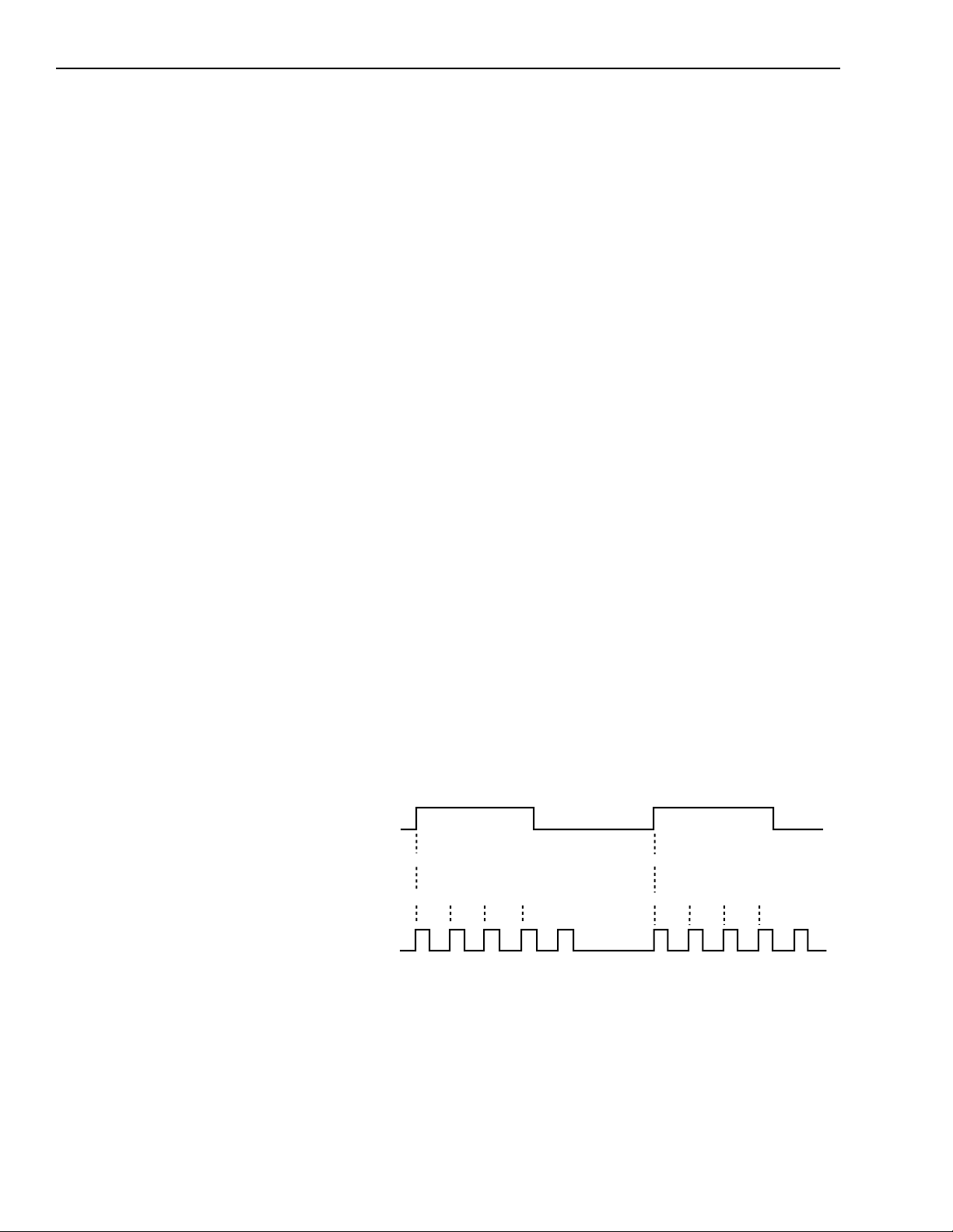
2-12 Functional Description KPCI-3108 Series User’s Manual
Data conversion modes
KPCI-3108 boards support two data-conversion modes: paced mode and burst mode. The conversion rate for each mode is controlled by an independent clock: the pacer clock for paced
mode and the burst clock for burst mode.
Paced conversion mode
The paced mode, which is the default data-conversion mode, is the best mode for continuous,
constant-rate scanning of each channel in a queue of channels. In the paced mode, one channel
in the channel-gain queue is sampled and converted each time the pacer clock emits a pulse. The
entire channel-gain queue is scanned at a rate equal to the pacer clock rate divided by the number of channels in the queue. Therefore, the sample rate — the rate at which an individual channel in the queue is repetitively sampled — is also equal to the pacer clock rate, divided by the
number of channels in the queue. See Figure 2-4. The internal pacer clock is programmable via
DriverLINX.
Burst conversion mode
The burst conversion mode is the best mode to use if you need to complete scans of the entire
channel-gain queue quickly — close to simultaneously — and initiate scans of the entire queue
at a significantly lower rate. For example, you would use the burst mode if you wish to complete
scans of the entire queue at 1000 conversions/sec but initiate scans of the entire queue only every
second.
In the burst mode, each pulse from the pacer clock initiates a burst of pulses from the burst clock
which are emitted at the burst clock rate. Each pulse from the burst clock causes one channel in
the queue to be sampled and converted, and burst clock pulses continue until the entire queue is
scanned. In summary, scans of the channel-gain queue are repetitively initiated at a rate equal to
the pacer clock rate, and scans of the queue are completed at a rate equal to the burst clock rate.
Therefore, the sample rate — the rate at which an individual channel in the queue is repetitively
sampled — is also equal to the pacer clock rate. See Figure 2-4.
Figure 2-4
Paced mode and burst mode timing for a queue of channels 4 to 7
Pacer Clock
Paced Mode Conversions
Burst Mode Conversions
CH4
CH4 CH5 CH6 CH7 CH4 CH5 CH6 CH7
CH5
Burst Clock
Page 36

•
•
•
KPCI-3108 Series User’s Manual Functional Description 2-13
Clock sources
KPCI-3108 boards provide two conversion clocks: a pacer clock and a burst mode clock. The
use of these clocks in the paced and burst conversion modes is described in “Data conversion
modes” and summarized in Figure 2-4. The clock sources themselves are described in the following subsections.
Pacer clock sources
The following clock sources may be used for paced mode conversions on KPCI-3108 boards:
Software clock source
KPCI-3108 boards allow you to acquire single samples under program control. In other
words, conversions are controlled through the Windows interface rather than by hardware
signals. When using a software conversion clock, the host computer issues a command to initiate a conversion. The host polls the board to determine if the conversion is complete. When
the conversion is complete, the host reads the data from the A/D converter and returns the
value.
Software-initiated conversions are suitable for measuring DC voltages. However, in applications where you must accurately control the sampling rate (as when measuring time-varying
signals), using either an internal or external hardware clock source is recommended, as
described below.
Hardware clock source, internal (Internal pacer clock source)
The internal, onboard pacer clock source creates a pacer-clock timing signal using one or
more 82C54 counter/timers and a crystal-controlled time base. (Refer to “Counter/timer features,” near the end of Section 2, for an illustration.) The time base runs at 10MHz and provides divided frequencies of 5 MHz, 1 MHz, and 100 kHz. You can program the internal
pacer clock rate via DriverLINX.
You can use the internal pacer clock source to pace events other than analog-to-digital conversions (digital-to-analog conversions, for example). However, all events timed by the internal pacer clock source are paced at the same rate.
Hardware clock source, external (External pacer clock source)
An external pacer clock source is an externally applied TTL-compatible signal attached to
bit IP0— pin 21 of the upper, “Analog” I/O connector, J1. Bit IP0 is a multi-function digital
input; therefore you must use software to configure it as the external pacer clock (XPCLK)
input. Also use software to select the active edge of the signal to be recognized as a clock
pulse — either a positive, rising edge or a negative, falling edge.
By using an external pacer clock source, you can sample at rates unavailable through the
82C54 counter/timer, at uneven intervals, or in response to external events. An external pacer
clock source also allows you to synchronize multiple boards via a common timing signal.
You can use the external pacer clock source in the paced conversion mode to pace individual
analog-to-digital and/or digital-to-analog conversions. You can use the external pacer clock
source in the burst conversion mode to pace space bursts of conversions. Refer to Figure 2-4.
NOTE
The A/D converter converts samples at a maximum of 100 ksamples/s
(one sample every 10.0µs), and the practical throughput is lower in
some applications. (Refer to the previous section entitled “Throughput”). If you use an external clock, ensure that it does not initiate conversions more frequently than the maximum throughput for your data
acquisition setup.
Page 37

•
•
•
•
2-14 Functional Description KPCI-3108 Series User’s Manual
Triggers
NOTE
NOTE
Keep in mind that the maximum sample rate for an individual channel
equals the maximum throughput divided by the number of channels in
the channel-gain queue.
You cannot simultaneously use an external pacer clock source and the
internal pacer clock source. However, you can simultaneously use a
software trigger source to start analog input conversions while simultaneously using either an internal or external pacer clock sour ce for other
I/O operations.
Burst clock source
In the burst mode, the burst clock sets the rate at which burst pulses are emitted and individual
channels in the channel-gain queue are converted. The burst clock works with the pacer clock,
which sets the rate at which groups of burst pulses are initiated. See Figure 2-4.
Burst clock and pacer clock frequencies are programmable, as follows:
The burst clock rate can be set via DriverLINX. The maximum acceptable burst mode conversion clock rate is gain-sensitive, as explained in “Throughput.”
The pacer clock rate should be set no higher than the burst clock rate divided by the number
of channels in the channel-gain queue.
Triggers are external digital signals or, in some cases, threshold crossings of analog signals.
Triggers act at a single instant in time, in contrast to gates, which start analog input operations
when the gate is turned on and stop the input operations when the gate is turned off. (Refer also
to “Gates” in this section.)
Trigger sources
Trigger sources may be internal or external, as follows:
Internal triggers
An internal trigger is a software command that starts or stops data acquisition.
External digital triggers
An external digital trigger is the rising or falling edge of a TTL-compatible signal that is connected to bit IP1—pin 3 of the upper, “Analog” I/O connector. Bit IP1 is a multi-function
digital input; therefore you must use software to configure it as the trigger-in (TGIN) input.
Also use software to program whether analog input operations start on either positive or negative triggering, which are defined as follows:
– Positive-edge triggering — Triggering occurs on the rising edge of the trigger signal.
– Negative-edge trigger ing — Triggering occurs on the falling edge of the trigger signal.
Page 38

KPCI-3108 Series User’s Manual Functional Description 2-15
•
Analog triggers
An analog trigger is an event that occurs at a rising or falling voltage level on an analog input
signal. Two software-selectable voltages specify where the analog trigger occurs: the trigger
level and the threshold level. As shown in Figure 2-5 , if the threshold level is greater than the
trigger level, triggering occurs on a negative slope. If the threshold level is less than the trigger level, triggering occurs on a positive slope.
In the KPCI-3108, an analog trigger works specifically in the about-trigger acquisition mode.
The acquisition is started by another internal or external trigger and continues after the analog trigger event until a specified number of samples has been acquired. For more information concerning about-trigger acquisition, refer to “Trigger acquisition modes” later in
Section 2.
Refer to your DriverLINX documentation for information about programming and configuring analog triggers.
Figure 2-5
Examples of analog trigger conditions
a. Negative-Slope Triggering b. Positive-Slope Triggering
Threshold level greater
than trigger level
Trigger
Level
+3V
0V
Negative-slope trigger
event occurs
Positive-slope trigger
event occurs
Threshold level less
than trigger level
Page 39
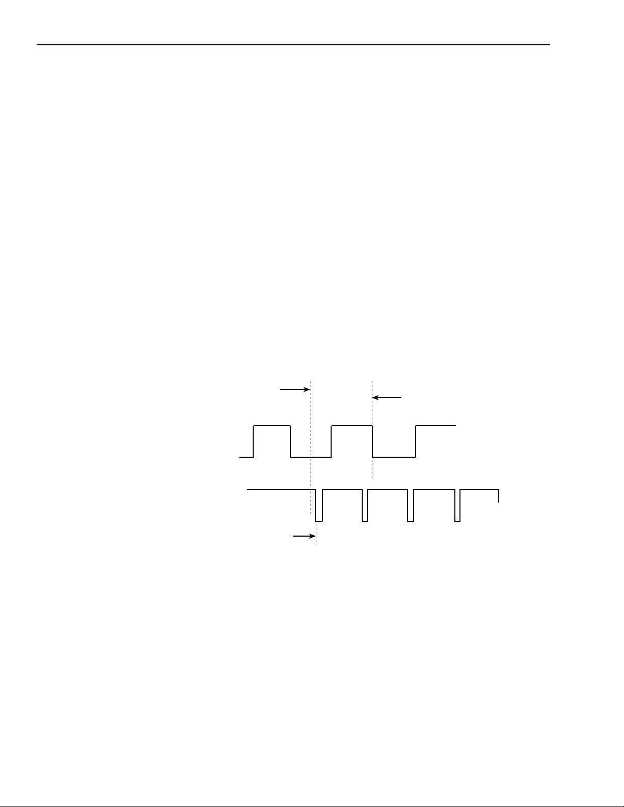
2-16 Functional Description KPCI-3108 Series User’s Manual
Trigger operation and clock source effects
The actual point at which conversions begin depends on whether the clock source is internal or
external, as follows:
• Internal trigger operation with internal clock source
If conversions are triggered with an internal trigger and timed via an internal pacer clock
source, then conversions begin virtually immediately after the trigger, as follows:
1. The 82C54 counter/timer is idle until the internal trigger occurs; after the trigger occurs,
the first conversion begins virtually immediately.
2. Subsequent conversions are synchronized to the internal clock.
See Figure 2-6.
• Internal trigger operation with external clock source
If conversions are triggered with an internal trigger and timed via an external clock source,
then analog input operations are triggered as follows:
1. Conversions are armed when the trigger occurs.
2. Conversions begin with the next active edge of the external clock source.
3. Conversions continue with subsequent active edges of the external clock source.
See Figure 2-6.
Figure 2-6
Enabling conversions with software triggers
Software enables
conversion process
External Clock Source
Internal Clock Source
Idle State
Conversions begin with
internal clock source
Conversions begin with
external source (programmed
for negative edge)
CountCount Count Count
• External trigger operation with internal clock source
If conversions are triggered with an external trigger and timed via an internal pacer clock
source, then analog input operations are triggered as follows:
1. Conversions begin virtually immediately after the internal trigger:
2. The 82C54 counter/timer is idle until the internal trigger occurs. However, after the trigger occurs, the first conversion begins within 400ns.
3. Subsequent conversions are synchronized to the internal clock.
See Figure 2-7.
Page 40
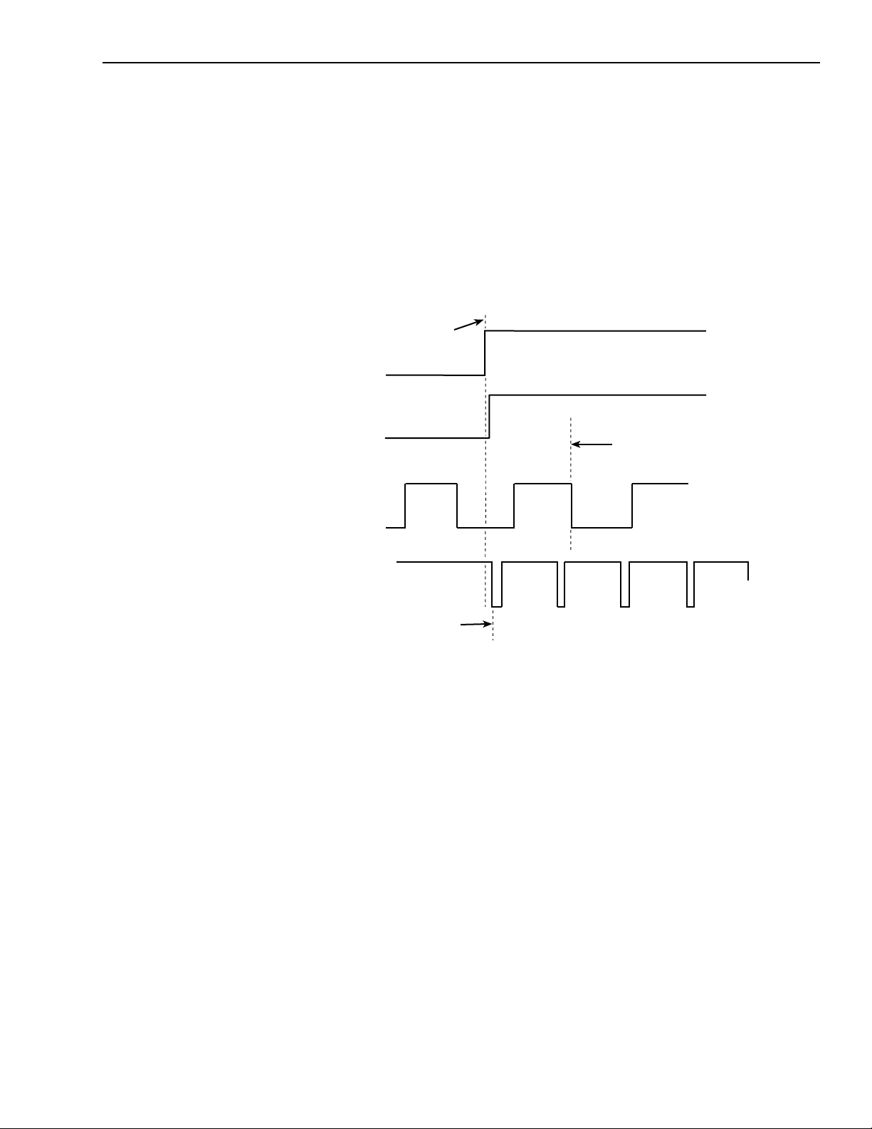
KPCI-3108 Series User’s Manual Functional Description 2-17
• External trigger operation with external clock source
If conversions are triggered with an external trigger and timed via an external clock source,
then analog input operations are triggered as follows:
1. Conversions are armed when the trigger occurs.
2. Conversions begin with the next active edge of the external clock source.
3. Conversions continue with subsequent active edges of the conversion clock.
See Figure 2-7.
Figure 2-7
Enabling conversions with hardware triggers
Trigger occurs (on positive edge)
TGIN Input
TGOUT Output
External Clock Source
Internal Clock Source
Conversions begin with
internal clock source
Idle State
Count Count Count Count
Conversions begin with
external source (programmed
for negative edge)
Figure 2-7 also shows that a pulse is initiated at the trigger out (TGOUT) digital output just following the external trigger pulse at the TGIN trigger input (the IP1 multi-function input configured as TGIN). For more information about TGOUT, refer to the section “The trigger-out
(TGOUT) digital output function.”
Page 41

2-18 Functional Description KPCI-3108 Series User’s Manual
Trigger acquisition modes
Depending on your application, you may wish to use a trigger event to do one of the following:
to start data collection, to halt data collection after a specified amount of additional data is collected, or to halt data collection abruptly. Three trigger modes are available in the KPCI-3108 to
accomplish these objectives.
• Post-trigger acquisition mode
In post-trigger acquisition, the data to be acquired appears after the trigger event. Posttrigger acquisition, starts after an internal or external trigger event and continues until a
specified number of samples has been acquired or until the operation is stopped by software.
See Figure 2-8a. Post-trigger, the most common trigger acquisition mode, has many obvious
applications.
• About-trigger acquisition mode
In about-trigger acquisition, the data to be acquired appears before and after the trigger
event. About-trigger acquisition is started by an internal or external trigger and continues
after an external trigger event until a specified number of samples has been acquired. See
Figure 2-8b. For example, if you were performing a car crash safety test, you might wish to
do the following:
1. Monitor speed and acceleration up to the point of impact.
2. Emit an accelerometer-based trigger pulse at impact.
3. Monitor crash-dummy impact forces and movement for a fixed number of samples after
impact.
• Pre-trigger acquisition mode
In the pre-trigger acquisition mode, the data to be acquired appears before the trigger event.
A pre-trigger acquisition is started by an internal or external trigger and continues until an
external trigger event occurs. See Figure 2-8c. For example, if you were monitoring an
experimental process, you might wish to trigger process data acquisition to stop automatically at completion of the process.
Page 42

KPCI-3108 Series User’s Manual Functional Description 2-19
Figure 2-8
Trigger acquisition modes
a. Post-Trigger Acquisition
Conversions Occurring
Conversions Stopped
Gates
Conversions Occurring
Conversions Stopped
Conversions Occurring
Conversions Stopped
Internal or External Trigger
N Samples Done OR
Software Halt
b. About-Trigger Acquisition
N Samples
External Digital TriggerInternal or External Trigger
c. Pre-Trigger Acquisition
External Digital TriggerInternal or External Trigger
A gate is a digital input that allows conversions to proceed as long as the gate signal is active
(logic high) and causes conversions to be halted as long as the gate signal is inactive (logic low).
In other words, conversions can be started and stopped at will by turning the gate input on and
off. (By contrast, a trigger acts at a single instant in time. Refer also to “Triggers” in this
section.)
The gate input signal is a logic-high or logic-low TTL-compatible signal that is connected to bit
IP1—pin 3 of the upper, “Analog” I/O connector. Bit IP1 is a multi-function digital input bit.
Therefore you must software-configure it for gate input. This same input bit is used as the external trigger-in (TGIN) bit. However, it must be configured differently for the board to recognize
incoming signals as gate signals instead of as trigger signals.
Page 43
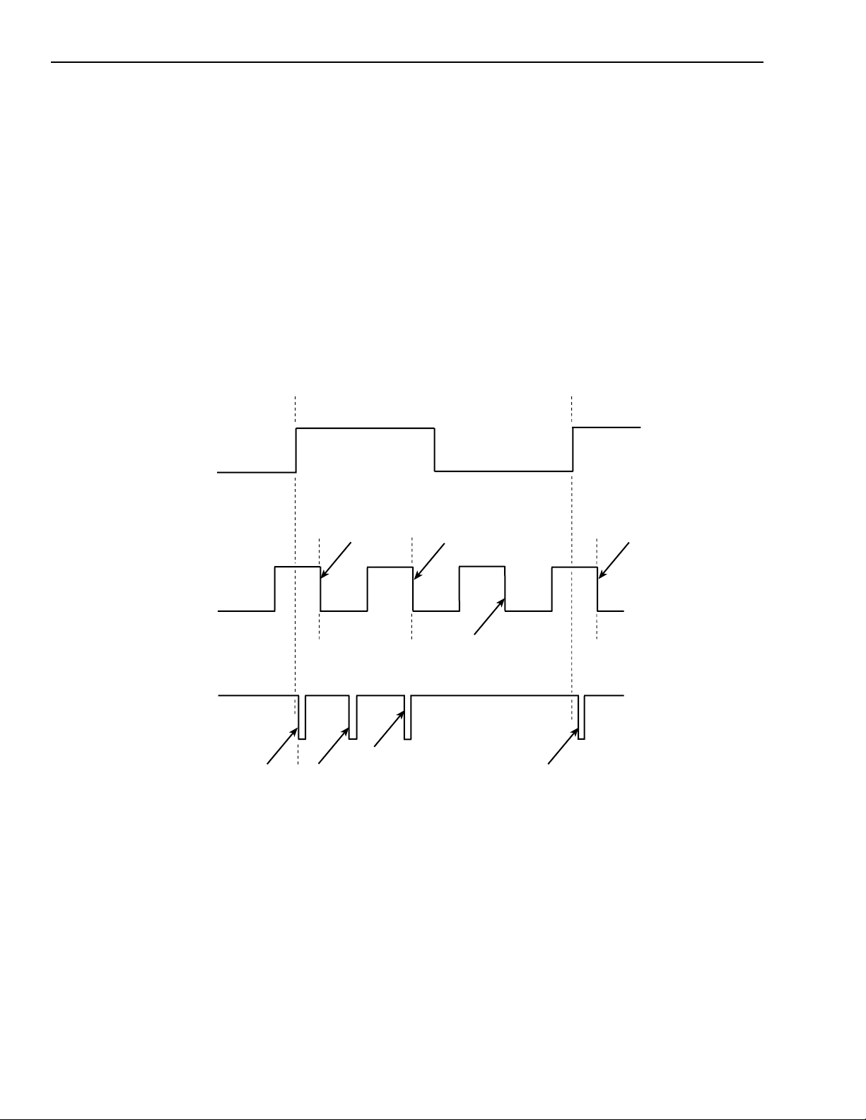
2-20 Functional Description KPCI-3108 Series User’s Manual
The way conversions are synchronized with a gate signal depends on whether you are using an
internal clock or external clock source, as follows:
• Gate operation with internal clock source
When using the gate input with an internal clock, conversions are synchronized with the
internal gate signal. When the gate signal becomes active, the 82C54 counter is loaded (or
reloaded) with an initial count value and starts counting, and data conversion starts (or
resumes). When the gate signal becomes inactive, the 82C54 counter stops and data conversion stops. See Figure 2-9.
• Gate operation with external clock source
When using the gate input with an external clock signal, conversions are synchronized with
the external gate signal. When the gate signal becomes inactive, the signal from the external
clock continues uninterrupted. See Figure 2-9.
Figure 2-9
Enabling conversions with gates
Digital Trigger
and Gate
Source
External Clock
Source
Internal Clock
Source
Gate Active;
Conversions On
3rd Conversion
1st Conversion 2nd Conversion
2nd Conversion1st Conversion
No Conversion
Gate Inactive;
Conversions Off
4th Conversion
Gate Active
3rd Conversion
Page 44

KPCI-3108 Series User’s Manual Functional Description 2-21
Analog output features
The analog output section of a KPCI-3108 board consists of two 16-bit DACs (digital-to-analog
converters). Each DAC has four software-selectable ranges, as listed in Table 2-3.
Table 2-3
Analog output ranges and resolutions
Range Resolution
±10.0 V 305 µV
±5.0 V 153 µV
0 to +10.0 V 153 µV
0 to +5.0 V 76 µV
The two DACs have output current ratings of ±5mA maximum and can drive capacitive loads of
up to 100mF. The DAC output always initiates to 0V at power-up or reset.
The digital-to-analog conversion options resemble the analog-to-digital conversion options. The
range and update sequence for one or both of the analog output channels is specified in a twoposition, maximum, channel-gain queue. Both paced and burst conversion modes are available,
as follows:
• In paced mode, one of the analog outputs specified in the channel gain queue is updated
every time a pacer clock signal occurs. The pacer clock signal can be any of the following:
– An internal hardware clock signal: an output pulse from an 82C54 counter/timer, the
clock input of which is connected to a crystal-controlled time base.
– An external hardware clock signal: the negative (falling) or positive (rising) edge of an
external clock pulse.
– A software update command: a write of an individual voltage value to a DAC by soft-
ware. (This method is sometimes referred to as “level control.”)
• In burst mode, both of the analog outputs specified in the channel-gain queue are sequen-
tially updated every time that a hardware (only) pacer clock signal occurs. A burst clock
determines the rate at which the updates occur. A typical user configures the burst clock rate
to be much higher than the pacer clock rate. However, the burst clock rate must always be at
least as large as the pacer clock rate times the number of positions (entries) in the channel
gain queue. The maximum burst clock rate for digital-to-analog conversions is 500 kHz.
Refer also to the A/D paced and burst mode conversion discussions under “Data conversion
modes” and “Clock sources” earlier in Section 2.
For information about wiring the analog outputs, refer to “Wiring analog output signals (KPCI3108 board only)” in Section 3. For information about configuring and using the analog outputs,
refer to your DriverLINX documentation and application software documentation.
Page 45

2-22 Functional Description KPCI-3108 Series User’s Manual
Digital input and output features
This section discusses the following:
• The 32 general-purpose digital inputs and outputs
• The six multi-function digital inputs and six multi-function digital outputs, including:
– Bit assignment options
– Special functions
KPCI-3108 boards have 32 general-purpose digital inputs and outputs, six multi-function digital
inputs, and six multi-function digital outputs. The general-purpose digital I/O and multi-function
digital I/O are discussed in separate sections below
NOTE For all digital I/O, logic 1 on an I/O line indicates that the input/output
is high (greater than 2.0V); logic 0 on an I/O line indicates that the
input/output is low (less than 0.8V). The digital inputs are compatible
with TTL-level signals. Multi-function digital inputs (IPO-IP5 on the
analog connector) are provided with 10kΩ pull-up resistors connected
to +5V; therefore, multi-function digital inputs appear high (logic 1) if
no signal is connected. The 32 general purpose inputs and outputs on
the digital connector do not include any pull-up resistor.
General-purpose digital inputs and outputs
The lower, “Digital” I/0 connector provides 32 bits of high current I/O (15 mA max. source
current at ≥2.0V, 64 mA max. sink output current at <0.55V). These general-purpose bits (the
twelve multi-function digital I/O bits available at the upper “Analog” I/O connector may also be
configured as general-purpose bits) are software-configurable as either inputs or outputs in
groups of eight—each group of eight bits being handled by one of four eight-bit registers. These
bits may be used for a variety of purposes, similarly to the bits of common digital I/O boards
such as the PIO-24 and KPCI-PIO24. The output current capabilities of these bits are much
higher than available from the industry-standard 8255 digital I/O chip.
Connector pin assignments for general-purpose digital I/O bits are summarized in Figure 3-3 of
Section 3. Wiring of the general-purpose digital I/O is discussed in Section 3, specifically under
“Wiring digital input and output signals” and generally under “Installing and wiring to the
KPCI-3108 board.” The electrical characteristics of the general purpose digital I/O are listed in
Appendix A. Programming/configuring and using the general-purpose digital I/O is discussed in
your DriverLINX documentation and/or your application software documentation.
Page 46

KPCI-3108 Series User’s Manual Functional Description 2-23
Multi-function digital inputs and outputs
The upper “Analog” I/O connector provides twelve multi-function TTL I/O bits. Six of the bits,
IP0 through IP5, are fixed as inputs (CMOS, as well as TTL, compatible). The other six bits,
OP0 through OP5, are fixed as outputs.
Each of the six multi-function input bits may be used as a general-purpose digital input bit, or as
a counter/timer access or acquisition control bit. Refer to Table 2-4.
Table 2-4
Specific bit assignments and descriptions for multi-function digital inputs
Bit assignment Description
IP0 May be used as the following:
• XPCLK, external pacer clock input
• General-purpose input bit, target mode
IP1 May be used as the following:
• TGIN, external trigger or gate input
• General-purpose input bit, target mode
IP2 May be used as the following:
• Counter/timer C/T0 external clock input
• General-purpose input bit, target mode
IP3 May be used as the following:
• Counter/timer C/T1 external clock input
• General-purpose input bit, target mode
IP4 May be used as the following:
• Counter/timer C/T0 external gate input
• General-purpose input bit, target mode
IP5 May be used as the following:
• Counter/timer C/T1 external gate input
• General-purpose input bit, target mode
When a multi-function digital input bit is configured as general-purpose input bits, data is transferred via a DriverLINX target-mode-read service request. However, a multi-function digital
input bit that is being used as a counter/timer access bit or acquisition control bit may also be
read via a target-mode-read, without interfering with the counter/timer access or acquisition
control function.
The functions of the first five multi-function output bits (OP0 through OP4) are configured in
fixed groups rather than individually. Refer to Table 2-5. There are three group configuration
modes: mode 0, mode 1, and mode 2. In any given mode, the bit functions of OP0 through OP4
are fixed; bit functions from the other two modes cannot be interlaced or overlapped.
• Mode 0 is the general-purpose output mode. In mode 0, outputs OP0 through OP4 can be
used as target-mode digital outputs. The bits are set and cleared via a DriverLINX service
request.
• Mode 1 is the counter/timer and acquisition-control output mode. In mode 1, outputs OP0
through OP4 provide access to all three counter/timer outputs and to two key acquisitioncontrol outputs.
• Mode 2 is the multiplexer control mode. In mode 2, outputs OP0 through OP4 control
address and gain selection of external multiplexers, as used in channel-expansion accessories
such as the EXP-1800 and MB-02.
Page 47

2-24 Functional Description KPCI-3108 Series User’s Manual
However, the sixth multi-function output bit (OP5) is configured individually—independently of
mode 0, mode 1, and mode 2—for any of a variety of special functions. This bit gives you access
to TGOUT, an output that tracks the pacer-clock, or the output of one counter/timer, even when
controlling external multiplexers. Refer to Table 2-5.
Table 2-5
Specific bit assignments and descriptions for multi-function digital outputs
Bit
Output
mode
0 OP0 General-purpose output bit, target-mode
assign-
ment Description
OP1 General-purpose output bit, target-mode
OP2 General-purpose output bit, target-mode
OP3 General-purpose output bit, target-mode
OP4 General-purpose output bit, target-mode
OP5 Configurable as one of the following:
• TGOUT (trigger-out output)
• Pacer clock output
• Counter/timer C/T0, CT1, or CT2 output
1 OP0 Frame sync
OP1 Counter/timer C/T0 output
OP2 Counter/timer C/T1 output
OP3 Counter/timer C/T2 output
OP4 Pacer-clock output
OP5 Configurable as one of the following:
• TGOUT (trigger-out) output
• Pacer clock output
• Counter/timer C/T0, CT1, or CT2 output
2 OP0 External address bit 0 for multiplexing of expansion-accessory channels
OP1 External address bit 1 for multiplexing of expansion-accessory channels
OP2 External address bit 2 for multiplexing of expansion-accessory channels
OP3 External address bit 3 for multiplexing of expansion-accessory channels
OP4 External gain bit for some expansion accessories (e.g. EXP-1800)
OP5 Configurable as one of the following:
• TGOUT (trigger-out output)
• Pacer clock output
• Counter/timer C/T0, CT1, or CT2 output
Connector pin assignments for the multi-function digital I/O bits are summarized in Figure 3-2.
Wiring to the multi-function digital I/O is discussed in Section 3 under “Wiring digital input and
output signals.” Electrical characteristics of the multi-function digital I/O are listed in Appendix
A. Configuring/programming and using the multi-function digital I/O is discussed in your
DriverLINX documentation and/or your application software documentation.
Software-configurable special functions for the multi-function digital I/O are discussed briefly in
the subsections that follow.
Page 48

KPCI-3108 Series User’s Manual Functional Description 2-25
The external pacer clock (XPCLK) digital input function
You can configure multi-function bit IP0 as an external pacer-clock input (XPCLK). Then you
can connect this input to an external hardware-clock source to time analog data conversions.
You cannot use the external pacer-clock source and the internal pacer-clock source simultaneously. However, you can simultaneously use the software-clock source to start analog data
conversions while simultaneously using either an internal or external hardware-clock source.
For more information about the use of an external pacer clock, refer to the following headings
earlier in Section 2: “Data conversion modes,” “Clock sources,” and “Analog output features.”
The trigger in (TGIN) digital input function
You can configure multi-function bit IP1as an external digital trigger input (TGIN) or gate input.
Then you can connect this input to an external TTL-compatible trigger or gate signal for starting
and/or stopping analog-to-digital conversions.
For more information about the use of an external trigger signal, refer to “Triggers” and “Gates”
earlier in Section 2.
The counter/timer clock digital input functions
Your board includes an 82C54 circuit that provides three counter/timers. You can configure the
following multi-function digital I/O bits on the upper “Analog” I/O connector as external
counter/timer clock inputs for two of the three 82C54 counter/timers:
• Bit IP2 is the external clock input for counter/timer C/T0.
• Bit IP3 is the external clock input for counter/timer C/T1.
There is no external counter/timer clock input for counter/timer C/T2
You can connect these inputs to external event or time base signals to perform a variety of tasks.
For more information about the use of the 82C54 counter/timers, refer to “Counter/timer features” later in Section 2.
The counter/timer gate digital input functions
Your board includes an 82C54 circuit that provides three counter/timers. You can configure the
following multi-function digital I/O bits on the upper “Analog” I/O connector as external
counter/timer gate inputs for two of the three 82C54 counter/timers.
• Bit IP4 is the external gate input for counter/timer C/T0.
• Bit IP5 is the external gate input for counter/timer C/T1.
There is no external counter/timer gate input for counter/timer C/T2
You can connect the C/T0 and C/T1 gate inputs to external TTL signals to enable or disable
C/T0 and C/T1.
For more information about the use of the 82C54 counter/timers, refer to “Counter/timer features” later in Section 2.
Page 49

2-26 Functional Description KPCI-3108 Series User’s Manual
The trigger-out (TGOUT) digital output function
You can configure bit OP5 as a trigger-out (TGOUT) digital output, which is synchronized with
internal and external trigger and gate signals.
If you use only the internal pacer clock to trigger analog I/O operations, you can use the TGOUT
signal to synchronize analog I/O operations at multiple KPCI-3108 boards. Alternatively, you
can use the TGOUT signal to trigger or gate user-specific events. The TGOUT signal has the following properties:
• TGOUT signal with an external trigger input signal
When you start an analog input operation with an external trigger signal (at bit IP1 configured as the TGIN input), there is a delay of about 200ns between the active edge of the TGIN
signal and the positive, rising edge of the TGOUT signal. See Figure 2-10a.
NOTE TGOUT cannot be used with about-trigger acquisitions.
• TGOUT signal with an external gate input signal
When you start an analog input operation via an external gate signal (at bit IP1 configured as
a gate input), there is a delay of about 200ns between the active edge at IP1 and the positive,
rising edge of TGOUT. See Figure 2-10b.
• TGOUT signal with an internal trigger or gate signal
When you start an analog input operation via an internal trigger/gate, there is a delay of less
than 1µs between the active edge of the internal trigger/gate and the positive, rising edge of
TGOUT. See Figure 2-10c.
You may configure bit OP5 for TGOUT individually, independently of the three output options
that configure the other five multi-function digital output bits (OP0 through OP4). Refer to
Table 2-5.
Figure 2-10
Timing for the generation of TGOUT
IP1, as Trigger
(TGIN)
TGOUT
IP1, as Gate
TGOUT
Software Enables
Conversions
Internal
Trigger/Gate
200ns Typical
a. External Trigger
200ns Typical
b. External Gate
< 1µs
Remains active until
conversions are
disabled by software
Software Disables
Conversions
TGOUT
c. Internal Trigger/Gate
Page 50

KPCI-3108 Series User’s Manual Functional Description 2-27
The pacer-clock output function
The KPCI-3108 boards provides a pacer-clock output that is synchronized with the internal or
external pacer clock, whichever is being used for A/D and/or D/A conversions. The external
pacer-clock output may be used to synchronize A/D and/or D/A conversions with the operation
of external devices connected to the board I/O connectors.
Under multi-function digital output option 0, configure bit OP4 as a pacer-clock output bit. You
may also individually configure bit OP5 as a pacer-clock output bit, independently of the three
output options that configure the other five multi-function digital output bits (OP0 through OP4).
Refer to Table 2-5.
Frame sync digital output signal
Frame sync is a digital output signal that goes low (logic 0) just after completion of a scan of the
channel-gain queue. This may be useful in the future for track and hold applications.
The counter/timer digital output functions
Your board includes an 82C54 circuit that provides three counter/timers. You can configure the
multi-function digital output bits on the upper “Analog” I/O connector as external counter/timer
clock outputs for all three 82C54 counter/timers, as follows:
• Bit OP1 is the external output for counter/timer C/T0.
• Bit OP2 is the external output for counter/timer C/T1.
• Bit OP3 is the external output for counter/timer C/T2.
You can connect these outputs to perform a variety of tasks.
For more information about the use of the 82C54 counter/timers, refer to “Counter/timer features” later in Section 2.
All three counter/timer outputs are simultaneously available when the board is configured for
multi-function digital output option 0. Additionally, you may individually configure bit OP5 as
the output for any of the counter/timers, independently of the three output options that configure
the other five multi-function digital output bits (OP0 through OP4). Refer to Table 2-5.
The expansion-channel digital output functions
When you connect EXP-1800 expansion accessories or MB-02 signal conditioning /expansion
accessories to your KPCI-3108 board, you must configure multi-function output bits as
addresses to sequence the expanded I/O channels. You configure bits OP0, OP1, OP2, and OP3
as expansion channel addresses when you select output option 1.You simultaneously configure
OP4 as an expansion accessory gain bit (required by some expansion accessories) when you
select output option 1.
Table 2-5 summarizes the bit assignments under multi-function digital output option 1.
Page 51

2-28 Functional Description KPCI-3108 Series User’s Manual
Counter/timer features
Each KPCI-3108 board includes an 82C54 circuit that contains three counter/timers:
C/T0, C/T1, and C/T2. This section briefly discusses:
• The purpose and use of the counter/timers in general
• The counter/timer operational modes available with the KPCI-3108 board
Counter/timer general discussion
Each of the three counter/timers may be used to count event pulses or timing pulses, such as
pulses from a precision time base. When the number of pulses it counts at its clock input equals
a preset number—set via software—the counter/timer emits an output signal that may be used
for a variety of purposes. For example, the output may be used as an event trigger, as a dividedfrequency timing signal, or as the clock input for a second, cascaded counter/timer. Counting is
either enabled continuously or is enabled or disabled through a gate input. Figure 2-11 illustrates
the inputs and outputs of the three 82C54 counter/timers as implemented with the KPCI-3108
board.
Figure 2-11
Counter/timer I/O available on KPCI-3108 boards
Clock Input
Gate Input
Clock Input
Gate Input
Clock Input (Internal Only)
Gate Input (Internal Only,
Always Enabled)
C/T0
C/T1
C/T2
Output
Output
Output
The following summarizes the basic functions of the counter/timer inputs and outputs:
• The Clock input receives the event or time-base pulses that are counted.
• The Gate input receives a signal that enables or disables the counting process.
• The Output signals that the specified count has been achieved.
C/T2 accepts only internal clock signals and is enabled only internally and continuously. However, C/T2 may be used to extend the range of CT/0 or CT/1 by cascading—counting output
pulses from CT/0 or CT/1.
A key application that illustrates use of the counter/timers is pacer-clock timing. When scanning
input channels, your board can use pacer-clock timing signals to regularly space individual analog-to-digital and/or digital-to-analog conversions or bursts of conversions. (Refer to “Data conversion modes,” “Clock sources,” and “Analog output features” earlier in Section 2.) Any of the
three counter/timers may be used for pacer-clock timing. Note, however, that 82C54 timer/
counters are not required for the burst-clock, which is generated by a different route. Production
of internally-generated pacer-clock timing pulses is illustrated in Figure 2-12.
Page 52

KPCI-3108 Series User’s Manual Functional Description 2-29
Figure 2-12
Using counter/timers for internal pacer-clock
a. Using one counter/timer for pacer-clock timing
Pulses from internal
crystal-clock time base
Internal Enable
b. Using two counter/timers, cascaded, for pacer-clock timing
Pulses from internal
crystal-clock time base
Internal Enable
C/T0, CT1 or
CT2
C/T0, CT1 or
CT2
Pacer-Clock
Timing Signal
Internal
Enable
C/T0, CT1 or
CT2
Pacer-Clock
Timing Signal
In this application, each counter acts as a frequency divider. For example, if in Figure 2-12a the
crystal-clock time base is configured for 1 MHz (10, 5, 1, and 0.1 MHz are available) and the
counter/timer is set for 100 counts, a pacer-clock timing pulse is emitted only once per 100 timebase pulses. Therefore, the time-base frequency is divided by 100, and the output frequency is
10 KHz. If in Figure 2-12b the crystal-clock time base is configured for 1 MHz, and both
counter/timers are set for 100 counts, the time-base frequency is divided by a factor of
(100 x 100), and the output frequency is 100 Hz.
Four of the multi-function digital input bits at the upper “Analog” I/O connector are indepen-
dently software-configurable as counter/timer inputs for C/T0 and C/T1, as follows:
• The external clock input for counter/timer C/T0 is bit IP2 (pin 20).
• The external clock input for counter/timer C/T1 is bit IP3 (pin 2).
• The external gate input for counter/timer C/T0 is bit IP4 (pin 19).
• The external gate input for counter/timer C/T1 is bit IP5 (pin 1).
You can attach a 0 MHz to100 kHz external clock source to the clock inputs. Pull-up resistors of
10 kΩ are provided at the gate input pins; therefore, the gates appear enabled if no signal is
attached to the gate inputs.
The following three multi-function digital output bits are configured as counter/timer outputs —
together as a group — under output option 0:
• The output bit for counter/timer C/T0 is OP1 (pin 6 at the upper “Analog” I/O connector).
• The output bit for counter/timer C/T1 is OP2 (pin 23 at the upper “Analog” I/O connector).
• The output bit for counter/timer C/T2 is OP3 (pin 5 at the upper “Analog” I/O connector).
Additionally, multi-function digital output bit OP5 is independently configurable as C/T0, C/T1,
or C/T2 (at pin 4 at the upper “Analog” I/O connector).
For more information about multi-function digital output options, refer to the section above,
“Multi-function digital inputs and outputs.” Refer also to “Wiring counter/timer signals” in
Section 3.
Page 53

2-30 Functional Description KPCI-3108 Series User’s Manual
Counter/timer operational modes
The 82C54 counter/timer circuit provides software-configurable operational modes to perform
various functions. The following modes are available from the 82C54 counter/timer. All may not
be available for use with the KPCI-3108 board. Refer to your DriverLINX documentation to
determine which modes are available.
• Pulse on terminal count (Mode 0)
• Programmable one-shot (Mode 1)
• Rate generator (Mode 2)
• Square-wave generator (Mode 3)
• Software-triggered strobe (Mode 4)
• Hardware-triggered strobe (Mode 5)
Each of these modes is explained briefly in the subsections that follow. Refer to the DriverLINX
Counter/Timer Programming Guide for more details.
Pulse on terminal count (counter/timer mode 0)
The pulse-on-terminal-count mode is useful for event counting or for programming a time delay.
Software is used to force the output low. On the next clock pulse after the software writes the initial count value, the counter is loaded. When the counter reaches zero, the output goes high and
remains high until the software writes a new count value. Note that the output does not go high
until n + 1 clock pulses after the initial count is written, where n indicates the loaded count.
A high gate input enables counting; a low gate input disables counting. The gate input has no
effect on the output. Note that an initial count value written while the gate input is low is still
loaded on the next clock pulse.
Figure 2-13 illustrates pulse-on-terminal-count mode.
Figure 2-13
Pulse-on-terminal-count counter/timer mode
Clock Pulse
Software forces
output low
Output
Software writes initial
count value of 3
32 1
Page 54

KPCI-3108 Series User’s Manual Functional Description 2-31
Programmable one-shot (counter/timer mode 1)
The programmable one-shot mode is useful for providing a hardware-triggered delay or oneshot pulse. The output is initially high. A trigger loads the initial count value into the counter. At
the next clock pulse after the trigger, the output goes low and remains low until the counter
reaches zero. (The one-shot pulse is n clock cycles in duration, where n indicates the loaded
count.) After the counter reaches zero, the output goes high and remains high until the clock
pulse after the next trigger; this makes the one-shot pulse retriggerable.
You do not have to reload the count into the counter. The gate input has no effect on the output.
Writing a new count to the counter during a one-shot pulse does not affect the current one-shot
pulse.
Figure 2-14 illustrates programmable one-shot mode.
Figure 2-14
Programmable one-shot counter/timer mode
Clock Pulse
Trigger loads initial
count value of 3
Output
32 1
Rate generator (counter/timer mode 2)
The rate-generator mode is useful for generating a real-time clock interrupt. The output is initially high. A trigger loads the initial count value into the counter. At the next clock pulse after
the trigger, the counter starts counting down. When the counter reaches one, the output goes low
for one clock pulse and then goes high again. The counter is then reloaded with the initial count
value and the process repeats.
A high gate input enables counting; a low gate input disables counting. If the gate goes low during an output pulse, the output is set high immediately; this allows you to use the gate input to
synchronize the counter.
Writing a new count to the counter while counting does not affect the current counting sequence.
In this mode, a count of 1 is illegal.
Figure 2-15 illustrates rate generator mode.
Figure 2-15
Rate-generator counter/timer mode
Clock Pulse
Output
Trigger loads initial
count value of 3
3213 212
Page 55

2-32 Functional Description KPCI-3108 Series User’s Manual
Square-wave generator (counter/timer mode 3)
This mode is useful for square-wave generation. The output is initially high. A trigger loads the
initial count value into the counter. At the next clock pulse after the trigger, the counter starts
counting down. When half the initial count has elapsed, the output goes low for the remainder of
the count. When the total count elapses, the counter is reloaded with the initial count value, the
output goes high again, and the process repeats. If the initial count is odd, the output is high for
(n + 1) / 2 counts and low for (n - 1) / 2 counts, where n indicates the loaded count.
A high gate input enables counting; a low gate input disables counting. If the gate goes low
while the output is low, the output is set high immediately; this allows you to use the gate input
to synchronize the counter.
Figure 2-16 illustrates square-wave generator mode.
Figure 2-16
Square-wave generator counter/timer mode
Clock Pulse
Trigger loads initial
count value of 4
Output
43214321
Software-triggered strobe (counter/timer mode 4)
When the counter/timer is in the software-triggered strobe mode, the output is initially high.
Writing the initial count through software loads the initial count value into the counter at the
next clock pulse, but the counter does not start counting. At the next clock pulse, the counter
starts counting down. When the counter reaches zero, the output goes low for one clock pulse
and then goes high again. Note that the output does not go low until n + 1 clock pulses after the
initial count is written, where n indicates the loaded count.
A high gate input enables counting; a low gate input disables counting. The gate input has no
effect on the output.
Figure 2-17 illustrates software-triggered strobe mode.
Figure 2-17
Software-triggered strobe counter/timer mode
Clock Pulse
Software writes intial
count value of 3
Output
Software loads counter
with initial count
321
Page 56
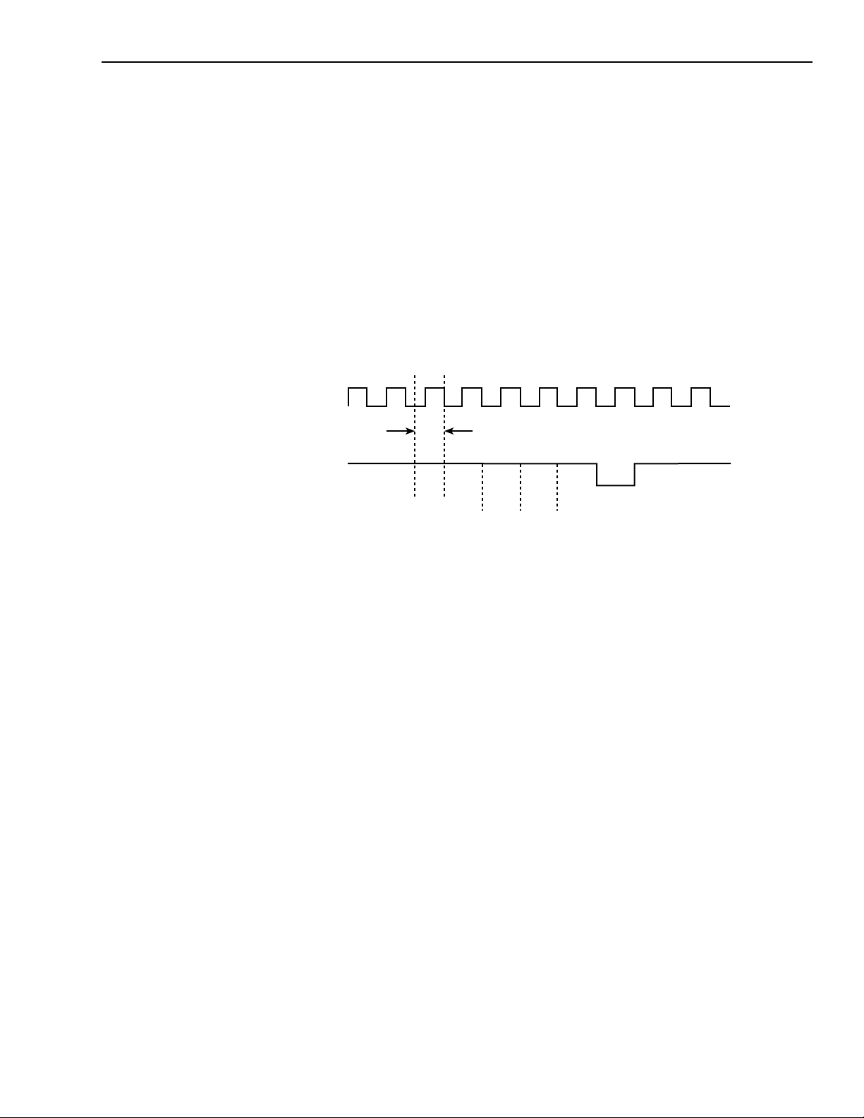
KPCI-3108 Series User’s Manual Functional Description 2-33
Hardware-triggered strobe (counter/timer mode 5)
When the counter/timer is in the software-triggered strobe mode, the output of the counter/timer
is initially high. A rising edge of the gate input acts as a trigger. The counter is loaded with the
initial count value on the next clock pulse after the trigger, but the counter does not start counting. At the next clock pulse, the counter starts counting down. When the counter reaches zero,
the output goes low for one clock pulse and then goes high again. Note that the output does not
go low until n + 1 clock pulses after the trigger event occurs, where n indicates the loaded count.
After the trigger event occurs, the gate input has no effect on the output. Writing a new value
during counting does not affect the counting sequence.
Figure 2-18 illustrates hardware-triggered strobe mode.
Figure 2-18
Hardware-triggered strobe counter/timer mode
Clock Pulse
Power
Rising edge of gate
input acts as trigger
Output
A KPCI-3108 board requires +5V at 0.8A from the host computer power bus and +12V at 0.5A
from this power bus to operate onboard circuits.
Additionally, +5V power for light duty external circuits—at a maximum total current draw of
1A— may be drawn indirectly from the host computer power bus via the board I/O connectors.
The +5V is available at pin 25 of the upper “Analog” I/O connector and pins 35 and 36 of the
lower “Digital” I/O connector.
CAUTION Do not connect the +5V outputs to external power supplies. Con-
necting these outputs to external power supplies may damage the
external supplies, the board, and the computer.
Do not draw more than 1.0A, total, from all +5V outputs combined.
Drawing more than 1.0A, total, may damage the board. Also keep in
mind that the 5V output comes from the computer power bus. Know
the limits of the computer 5V power bus and the current drawn from
it by other boards and devices. Other demands on the 5V power bus
may limit the current drawn from your board to less than 1.0A.
Counter is loaded with
initial count value of 3
32 1
Page 57

3
lnstallation
Page 58

•
•
•
•
3-2 lnstallation KPCI-3108 Series User’s Manual
This section describes system installation, in the following order:
Software options and installation guidelines. (Note: install the software before installing the
hardware.)
Hardware installation, including the following:
– Unwrapping and inspecting the board
– Physically installing the board
– Checking the combined board and DriverLINX installation
– Identifying the I/O connector pins
– Wiring your circuits to the I/O connector pins (via the wiring accessories)
– Synchronizing multiple boards
– Powering your circuits from the board
Installing the software
NOTE
Software options
Users of KPCI-3108 boards have the following two software options. In both cases, the software
interfaces with your system via the DriverLINX software provided with your board:
The user can run a fully integrated data-acquisition software package such as TestPoint or
LabVIEW.
The user can write and run a custom program in Visual C/C++, Visual Basic, or Delphi,
using the programming support provided in the DriverLINX software.
A summary of the pros and cons of using integrated packages or writing custom programs is
provided in the Keithley Full Line Catalog.
The KPCI-3108 has fully functional driver support for use under Windows 95/98/NT.
DriverLINX driver software for Windows 95/98/NT
DriverLINX software, supplied by Keithley with the KPCI-3108 board, provides convenient
interfaces to configure analog and digital I/O modes without register-level programming.
Most importantly, however, DriverLINX supports those programmers who wish to create custom applications using Visual C/C++, Visual Basic, or Delphi. DriverLINX accomplishes foreground and background tasks to perform data acquisition. The software includes memory and
data buffer management, event triggering, extensive error checking, and context sensitive online help.
Install the DriverLINX software befor e installing the KPCI-3108 board.
Otherwise, the device drivers will be more difficult to install.
Page 59

•
•
•
•
•
•
•
•
•
•
KPCI-3108 Series User’s Manual lnstallation 3-3
DriverLINX provides application developers a standardized interface to over 100 services for
creating foreground and background tasks for the following:
Analog input and output
Digital input and output
Time and frequency measurement
Event counting
Pulse output
Period measurement
In addition to basic I/O support, DriverLINX also provides:
Built-in capabilities to handle memory and data buffer management.
A selection of starting and stopping trigger events, including pre-triggering, mid-point trig-
gering and post-triggering protocols.
Extensive error checking.
Context-sensitive on-line help system DriverLINX is essentially hardware independent,
because its portable APIs (Application Programming Interfaces) work across various operating systems. This capability eliminates unnecessary programming when changing operating
system platforms.
TestPoint
TestPoint is a fully featured, integrated application package that incorporates many commonly
used math, analysis, report generation, and graphics functions. The TestPoint graphical dragand-drop interface can be used to create data acquisition applications, without programming, for
IEEE-488 instruments, data acquisition boards, and RS232-485 instruments and devices.
TestPoint includes features for controlling external devices, responding to events, processing
data, creating report files, and exchanging information with other Windows programs. It provides libraries for controlling most popular GPIB instruments. OCX and ActiveX controls plug
directly into TestPoint, allowing additional features from third party suppliers.
TestPoint interfaces with your KPCI-3108 board through DriverLINX, using a driver that is provided by the manufacturer.
LabVIEW
LabVIEW is a fully featured graphical programming language used to create virtual instrumentation. It consists of an interactive user interface, complete with knobs, slide switches, graphs,
strip charts, and other instrument panel controls. Its data-driven environment uses function
blocks that are virtually wired together and pass data to each other. The function blocks, which
are selected from palette menus, range from arithmetic functions to advanced acquisition, control, and analysis routines. Also included are debugging tools, help windows, execution highlighting, single stepping, probes, and breakpoints to trace and monitor the data flow execution.
LabVIEW can be used to create professional applications with minimal programming.
™
™
A Keithley VI palette provides standard virtual instruments (VIs) for LabVIEW that interface
with your KPCI-3108 board through DriverLINX. The needed driver is provided on your DriverLINX CD-ROM.
Page 60

3-4 lnstallation KPCI-3108 Series User’s Manual
Installing DriverLINX
Refer to the instructions on the Read this first sheet and the manuals on the DriverLINX
CD-ROM, both shipped with your board, for information on installing and using DriverLINX.
Installing application software and drivers
Installing the TestPoint software and driver
The DriverLINX driver for TestPoint is provided as part of the TestPoint software. The driver
therefore installs automatically when you install TestPoint.
You can install TestPoint application software, made by Capital Equipment Corporation (CEC),
at any time — before or after installing DriverLINX and the KPCI-3108 board. For TestPoint
installation instructions, consult the manual provided by CEC.
NOTE
Before using TestPoint with the KPCI-3108 version of DriverLINX,
check with CEC to ensure that your version of TestPoint is compatible
with DriverLINX.
Installing the LabVIEW software and driver
A DriverLINX driver for LabVIEW is provided on your DriverLINX CD-ROM. The LabVIEW
driver does not install automatically when you install DriverLINX and your board. You must first
install the LabVIEW application program, then install the DriverLINX driver. Access the LabVIEW driver installation routine by starting setup.exe on the DriverLINX CD-ROM, then selecting LabVIEW
Consult the manual provided by National Instruments for LabVIEW installation instructions.
™
Support from the Install These DriverLINX components screen.
Page 61

KPCI-3108 Series User’s Manual lnstallation 3-5
Installing and wiring to the KPCI-3108 board
The remainder of this section describes physically installing the KPCI-3108 board, connecting
interfaces to the board, and wiring circuits to the interfaces. KPCI-3108 board connectors
involved in these operations are labeled in Figure 3-1.
Figure 3-1
Connectors on the KPCI-3108 board
Connector for
analog I/O and
multi-function
digital I/O
(labeled “Analog”)
KPCI-3108 Board
Connector for
general-purpose
digital I/O
(labeled “Digital”)
PCI-Bus Connector
The remainder of this section is ordered according to the following recommended installation
sequence:
1. Install the board in your computer, as described in “Installing the board.”
2. Check the installation as described in “Checking the combined board and DriverLINX
installations.”
3. Review the I/O connections for each pin on the two 36-pin I/O connectors of your board.
Connector pin assignments for the KPCI-3108 boards are identified and described under
“Identifying I/O connector pin assignments for KPCI-3108.”
4. Connect the appropriate screw terminal and other interface accessory(s) to your board, using
an appropriate cable assembly(s). One or more accessories are required to wire the board to
your circuits. These accessories range from basic screw terminal connectors (STP-36) to signal conditioning and expansion accessories. Use of interface accessories and cables is
described under “Connecting interface accessories to a KPCI-3108 board.”
5. Wire your circuits to the interface accessories that you connected to the board in step 4.
Refer to the sections “Wiring analog input signals,” “Wiring analog output signals (KPCI3108 board only),” “Wiring digital input and output signals,” and “Wiring counter/timer
signals.”
6. If you wish to synchronize multiple KPCI-3108 boards, interconnect the trigger or gate signals as described under “Synchronizing multiple boards.”
7. If you desire to use KPCI-3108 board power for any of your circuits, be sure to read “Wiring
+5V power to external circuits” before proceeding.
Page 62

3-6 lnstallation KPCI-3108 Series User’s Manual
Installing the board
CAUTION Ensure that the computer is turned OFF before installing or remov-
ing a board. Installing or removing a board while power is ON can
damage your computer, the board, or both.
Handle the board in a static-controlled workstation; wear a
grounded wrist strap. Discharge static voltage differences between
the wrapped board and the handling environment before removing
the board from its protective wrapper. Failure to discharge static
electricity before and during handling may damage semiconductor
circuits on the board.
Handle the board using the mounting bracket. Do not touch the circuit traces or connector contacts when handling the board.
Checking resources for the board
Ensure that your computer has sufficient resources, particularly power resources, to run your
KPCI-3108 board. Check the capacity of the computer power supply and the power requirements of your computer and presently installed boards. Adding a KPCI-3108 board requires an
additional 0.8A at +5V, maximum, and an additional 0.5A at +12V, maximum. If necessary, free
resources by uninstalling other boards.
Unwrapping and inspecting the KPCI-3108 board
NOTE
After you remove the wrapped board from its outer shipping carton, unwrap and inspect it as
follows:
1. Your board is packaged at the factory in an anti-static wrapper. Do not remove the anti-static
wrapper until you have discharged any static electricity voltage differences between the
wrapped board and the environment. Wear a grounded wrist strap. A grounded wrist strap
discharges static electricity from the wrapped board as soon as you hold it. Keep the wrist
strap on until you have finished installing the board.
2. Remove the KPCI-3108 board from its anti-static wrapping material. (You may wish to store
the wrapping material for future use.)
3. Inspect the board for damage. If damage is apparent, arrange to return the board to the factory. Refer to Section 6, “Technical support.”
4. Check the remaining contents of your package against the packing list and report any missing items immediately.
5. If the inspection is satisfactory, continue with “Installing the KPCI-3108 board.”
Install the DriverLINX software befor e installing the KPCI-3108 board.
Otherwise, the device drivers will be more difficult to install.
Installing the KPCI-3108 board
WARNING Be sure to reinstall the cover of your computer after installing the
board.
Install a KPCI-3108 board in a PCI expansion slot on your computer as follows:
1. Turn power OFF to the computer and to any external circuits attached to the board.
Page 63

KPCI-3108 Series User’s Manual lnstallation 3-7
2. Remove the computer chassis cover.
3. Select an unoccupied PCI expansion slot in the rear panel, and remove the corresponding
dummy mounting plate.
4. Insert the PCI connector of the board into the selected PCI slot of the computer. Take care
not to interfere with neighboring boards. Ensure that the board is properly seated in the slot.
5. Secure the mounting bracket of the board to the chassis, using the retaining screw that you
removed when you removed the dummy mounting plate.
6. Continue with “Configuring the board to work with DriverLINX.”
Configuring the board to work with DriverLINX
After physically installing the board, do the following:
1. Turn on and reboot the computer. The DriverLINX Plug and Play Wizard screen appears.
2. Run the Wizard immediately by following the progressive instructions on the screen.
3. Continue with “Checking the combined board and DriverLINX installations.”
If you do not run the Wizard immediately, it will not appear the next time you reboot. You must
then start the Wizard from a batch file, as follows:
1. Open the Windows Explorer.
2. Double click on X:\DrvLINX4\Help\kpci3108.bat, where X = the letter of the drive on
which you installed DriverLINX.
The Wizard appears.
NOTE
3. Run the Wizard by following the progressive instructions on the screen.
4. Continue with “Checking the combined board and DriverLINX installations.”
You can also start this batch file directly from the CD-ROM by double
clicking on Y:\DrvLINX4\Help\kpci3108.bat, where Y = the drive letter
of your CD-ROM drive.
Checking the combined board and DriverLINX installations
Before making any connections to the board, check whether DriverLINX and your board are
installed correctly and working together properly. Do this using the first two steps of “Problem
isolation Scheme B: installation” in Section 6. The first two steps evaluate whether the DriverLINX Analog I/O Panel utility starts properly. If the Panel does not start properly at first,
remaining steps lead you through diagnostic and remedial efforts. If necessary, steps lead you to
deinstall, then reinstall DriverLINX and the board.
Do the following:
1. Turn ON your computer and boot Windows 95, 98, or NT.
2. Perform the first two steps of “Problem isolation Scheme B: installation” in Section 6.
3. If you cannot initially run the Analog I/O Panel, perform additional steps of “Problem isolation Scheme B: installation” as directed.
4. After DriverLINX and your board are installed properly and working together, continue with
“Identifying I/O connector pin assignments for KPCI-3108,” and then “Connecting interface
accessories to a KPCI-3108 board.”
Page 64

•
3-8 lnstallation KPCI-3108 Series User’s Manual
Identifying I/O connector pin assignments for KPCI-3108
You connect a KPCI-3108 board to your signals via two IEEE 1284 36-pin mini-D connectors,
located at the rear of the board.
Figure 3-2 and Table 3-1 show and describe pin assignments and signal descriptions for the
upper “Analog” I/O connector, through which analog I/O and multi-function digital I/O
signals are connected. Identically numbered assignments and descriptions apply to the
terminals on either of the following (described in the next section) if it is connected to the
“Analog” I/O connector:
– An STP-36 Series screw-terminal accessory (STP-36)
– An STA-3108-A Series adapter/screw-terminal accessory (STA-3108-A1, STA-3108-A2,
STA-3108-A3)
Figure 3-2
Pin assignments for KPCI-3108 upper “Analog” I/O connector pin
IP5
IP3
IP1
OP5
OP3
OP1
DGND
CH07 LO/CH15 HI
CH06 LO/CH14 HI
CH05 LO/CH13 HI
CH04 LO/CH12 HI
CH03 LO/CH11 HI
CH02 LO/CH10 HI
CH01 LO/CH09 HI
CH00 LO/CH08 HI
No connection
AGND
AGND
10
11
12
13
14
15
16
17
18
IP4
1
2
3
4
5
6
7
8
9
19
IP2
20
IP0
21
OP4
22
OP2
23
OP0
24
+5 V
25
CH07 HI
26
CH06 HI
27
CH05 HI
28
CH04 HI
29
CH03 HI
30
CH02 HI
31
CH01 HI
32
CH00 HI
33
+10 V Reference
34
DAC1 Output
35
DAC0 Output
36
Page 65

•
•
•
•
•
•
•
•
•
•
•
•
•
•
•
•
•
•
•
•
•
•
•
•
•
•
KPCI-3108 Series User’s Manual lnstallation 3-9
Table 3-1
Signal descriptions for “Analog” I/O connector pins and screw-terminals
Pin or
terminal
1
2
3
4
5
6
7 DGND Digital ground.
8
9
10
:
15
16 No connection
17, 18 AGND Analog ground. (Refer to “Wiring analog input signals.”)
19
20
21
22
23
24
25 +5 V + 5 VDC from computer bus. (Refer to “Wiring +5V power to
26
27
28
:
33
34 +10 V Reference Precision +10 VDC reference voltage source, which is designed to
35 DAC1 Output* Analog output from digital-to-analog converter number 1*
36 DAC0 Output* Analog output from digital-to-analog converter number 0*
*This feature is not included with the KPCI-3107.
Assignment Description
IP5
IP3
IP1
OP5
OP3
OP1
CH07 LO/CH15 HI
CH06 LO/CH14 HI
CH05 LO/CH13 HI
:
CH00 LO/CH08 HI
IP4
IP2
IP0
OP4
OP2
OP0
CH07 HI
CH06 HI
CH05 HI
:
CH00 HI
Multi-function digital input bits, user-configurable for:
Counter/timer timebase and/or gate inputs
External pacer for A/D or D/A conversion
External digital trigger
Target-mode digital input
Multi-function digital output bits, user-configurable for:
Counter/timer outputs
Trigger output
Control/addressing for expansion and signal conditioning
accessories
Pacer clock output
Target-mode digital output
Analog inputs, which function
as follows for inputs configured
as differential:
Channel 07 low-level input
Channel 06 low-level input
Channel 05 low-level input
Channel 00 low-level input
Multi-function digital input bits, user-configurable for:
Counter/timer timebase or gate inputs
External pacer for A/D or D/A conversion
External digital trigger
Target-mode digital input
Multi-function digital output bits, user-configurable for:
Counter/timer outputs
Trigger output
Control/addressing for expansion and signal conditioning
accessories
Pacer clock output
Target-mode digital output
external circuits.”)
Channel 07 high-level input
Channel 06 high-level input
Channel 05 high-level input
:
Channel 00 high -level input
be connected to a high-impedance reference input only (supplied
through a 1 K
:
Ω
series resistor).
Analog inputs, which function
as follows for inputs configured
as single-ended:
Channel 15 high-level input
Channel 14 high-level input
Channel 13 high-level input
:
Channel 08 high-level input
Page 66

•
3-10 lnstallation KPCI-3108 Series User’s Manual
Likewise, Figure 3-3 and Table 3-2 show and describe pin assignments and signal descriptions for the lower “Digital” I/O connector, through which 32 bits of general-purpose, highcurrent digital I/O are connected. Identically numbered assignments and descriptions apply
to the terminals on either of the following (described in the next section) if it is connected to
the “Digital” I/O connector:
– An STP-36 screw-terminal accessory (STP-36)
– An STA-3108-D1 Series adapter/screw-terminal accessory
Figure 3-3
Pin assignments for KPCI-3108 lower “Digital” I/O connector pins
Bit 16
Bit 0
Bit 1
Bit 2
Bit 3
Bit 4
Bit 5
Bit 6
Bit 7
Bit 8
Bit 9
Bit 10
Bit 11
Bit 12
Bit 13
Bit 14
Bit 15
DGND
DGND
1
2
3
4
5
6
7
8
9
10
11
12
13
14
15
16
17
18
19
20
21
22
23
24
25
26
27
28
29
30
31
32
33
34
35
36
Bit 17
Bit 18
Bit 19
Bit 20
Bit 21
Bit 22
Bit 23
Bit 24
Bit 25
Bit 26
Bit 27
Bit 28
Bit 29
Bit 30
Bit 31
+5 V
+5 V
Page 67

KPCI-3108 Series User’s Manual lnstallation 3-11
Table 3-2
Signal descriptions for “Digital” I/O connector pins and screw-terminals
“Digital”
connector pin
or STP-36
terminal
1
2
3
:
8
9
10
11
:
16
17, 18 DGND Digital grounds. (Refer to “Wiring general-purpose digital I/O
19
20
21
:
26
27
28
29
:
34
35, 36 +5V + 5 VDC from computer bus. (Refer to “Wiring +5V power to
Bit
assignment Description
Bit 0
Bit 1
Bit 2
:
Bit 7
Bit 8
Bit 9
Bit 10
:
Bit 15
Bit 16
Bit 17
Bit 18
:
Bit 23
Bit 24
Bit 25
Bit 26
:
Bit 31
General-purpose digital I/O bits, channel 0. As a group, these 8
bits are user-configurable as either all inputs or all outputs. (The
8 bits comprise the register of a type 652 chip.)
General-purpose digital I/O bits, channel 1. As a group, these 8
bits are user-configurable as either all inputs or all outputs. (The
8 bits comprise the register of a type 652 chip.)
signals.”)
General-purpose digital I/O bits, channel 2. As a group, these 8
bits are user-configurable as either all inputs or all outputs. (The
8 bits comprise the register of a type 652 chip.)
General-purpose digital I/O bits, channel 3. As a group, these 8
bits are user-configurable as either all inputs or all outputs. (The
8 bits comprise the register of a type 652 chip.)
external circuits.”)
Page 68

•
•
•
•
•
3-12 lnstallation KPCI-3108 Series User’s Manual
Connecting interface accessories to a KPCI-3108 board
CAUTION The two I/O connectors of KPCI-3108 board, labeled “Analog” and
“Digital,” are mechanically identical. Ensure that you connect interface accessories and, indirectly, external circuits to the correct I/O
connector. Connecting interface accessories or external circuits to
the wrong connector may result in damage to the KPCI-3108 board,
the host computer, your external circuits, or all three.
Use combinations of the following interface accessories to wire your circuits to the KPCI-3108
I/O connectors
Basic screw-terminal accessories
Channel-expansion, signal-conditioning, or digital I/O accessories, combined with adapter/
screw-terminal accessories
Interconnection cables
Section 1 summarized the available interface accessories in Table 1-2, Table 1-3, and Table 1-4.
This section describes how to interconnect these accessories, as follows:
The first subsection describes the STP-36 (or STC-36/C) screw-terminal accessory and how
to connect it to your board.
The second subsection through the fifth subsection describe various channel expansion, signal conditioning, and digital I/O accessories and how to connect them to your KPCI-3108
board. Each of these accessories interfaces to your board through a specially-designed
adapter/screw-terminal accessory. The following topics are covered:
– Connecting EXP-1800 channel-expansion accessories to the KPCI-3108 board via an
STA-3108-A1 accessory
– Connecting an MB-01, MB-05, or STA-MB signal conditioning accessory to the KPCI-
3108 board via an STA-3108-A2 accessory
– Connecting an MB-02 signal conditioning/expansion accessory to the KPCI-3108 board
via an STA-3108-A3 accessory
– Connecting digital I/O accessories to the KPCI-3108 board via an STA-3108-D1
accessory
Page 69

•
•
–
–
–
KPCI-3108 Series User’s Manual lnstallation 3-13
NOTE
When using combination adapter/screw-terminal accessories
(STA-3108-A1, STA-3108-A2, STA-3108-A3, or STA-3108-D1) as
recommended in these subsections, wire to the screw terminals with
caution. Be aware of the following:
All of the screw terminals are connected to the same-numbered pins of a
KPCI-3108 “Analog” or “Digital” I/O connector.
When a channel-expansion, signal-conditioning, or digital I/O accessory(s) is
connected to the adapter/screw-terminal accessory, some of KPCI-3108 I/O
signals at these screw terminals are shared. In general, do not wire external
circuits to screw terminals that are shared. However, which screw terminals
are actually shared depends on the configuration of the channel-expansion,
signal-conditioning, or digital I/O accessory configuration. For example:
Each EXP-1800 expansion accessory or MB-02 expansion/signalconditioning accessory is connected to only one single-ended analog input
channel. Therefore, if the number of EXP-1800 or MB-02 accessories
connected to your board is “n,” as many as (16- n) single-ended channels
or (8 -n/2) differential channels, are not shared. Unshared channels may
be wired to external circuits at the screw terminals. However, be aware
that at least four multi-function digital outputs (five for the EXP-1800) are
always used for multiplexing and are therefore always shared.
The MB-01 and MB-05 signal-conditioning accessory and the PB-24, PB24SM, SSI0-24, and ERB-24 digital I/O accessories each accommodate up
to 24 plug-in modules. If you plug in fewer than 24 modules, the analog
I/O channels or digital I/O bits not associated with modules are not shar ed
and may be wired to external circuits at the screw terminals.
Even if filled with plug-in modules, an MB-05 signal-conditioning accessory never shares all analog I/O channels and none of the digital I/O
accessories ever shares all digital I/O bits. The remaining channels/bits
may be wired to external circuits at the screw terminals.
Before wiring external circuits, first review your configuration and the
instructions for your accessories. Also review the pin-to-pin correspondence between the KPCI-3108 I/O connector and the adapter connector
of your adapter/screw-terminal accessory, as it applies to your configuration. Pin-to-pin data is listed in one of the following tables: Table 3-5,
Table 3-7, or Table 3-10.
Page 70

3-14 lnstallation KPCI-3108 Series User’s Manual
Connecting an STP-36 screw terminal accessory to a KPCI-3108 board
The STP-36 accessory provides basic screw terminal wiring to the I/O connector of a
KPCI-3108 board. All of the screw terminals are connected to the same-numbered pins of a
KPCI-3108 “Analog” or “Digital” I/O connector. Figure 3-4 shows how the accessory connects
to the board.
Figure 3-4
Connecting STP-36 screw terminal accessories
Analog I/O and
Multi-Function
Digital I/O
KPCI-3108 Board
General
Purpose
Digital I/O
STP-36
Accessory
STP-36
Accessory
CAB-1284CC
Series Cable
CAB-1284CC
Series Cable
Page 71

KPCI-3108 Series User’s Manual lnstallation 3-15
As shown in Figure 3-4, use a CAB-1284CC Series cable to connect an STP-36 accessory to a
KPCI-3108. Available CAB-1284CC Series cables are listed in Table 3-3.
Table 3-3
CAB-1284CC Series cables
Cable Description
CAB-1284CC-1 IEEE-1284 type C-C round cable with shielded, twisted-pair conductors
and molded, 36-pin mini-Centronics connectors on each end. Length
is1m.
CAB-1284CC-2 Same as CAB-1284CC-1, except length is 2m.
The screw terminal numbers and assignments on an STP-36 accessory are identical to the pin
numbers and assignments on the KPCI-3108 I/O connector to which it is connected. Therefore,
when you connect an STP-36 to the upper “Analog” connector of a KPCI-3108 board, the screw
terminal assignments are as shown in Figure 3-5. When you connect an STP-36 to the lower
“Digital” connector of a KPCI-3108 board, the screw terminal assignments are as shown in
Figure 3-6. For descriptions of these pins and assignments, refer to Table 3-1 and Table 3-2
under “Identifying I/O connector pin assignments for KPCI-3108.”
Figure 3-5
Upper “Analog” screw terminal assignments
IP5
IP4
IP2
IP0
OP4
OP2
OP0
+5 V
CH07 HI
CH06 HI
CH05 HI
CH04 HI
CH03 HI
CH02 HI
CH01 HI
CH00 HI
+10 V Reference
DAC1 Output*
DAC0 Output*
19
2021
2223
24
25
26
27
28
2930
31
3233
34
3536
IP3
IP1
OP5
OP3
OP1
DGND
CH07 LO/CH15 HI
CH06 LO/CH14 HI
CH05 LO/CH13 HI
1012131415161718 11 123546789
CH04 LO/CH12 HI
CH03 LO/CH11 HI
CH02 LO/CH10 HI
CH01 LO/CH09 HI
CH00 LO/CH08 HI
No connection
AGND
AGND
*Not available when connected to KPCI-3107.
Page 72

3-16 lnstallation KPCI-3108 Series User’s Manual
Figure 3-6
Lower “Digital” screw terminal assignments
Channel 3
Channel 4
Bit 16
Bit 17
Bit 18
Bit 19
Bit 20
Bit 21
Bit 22
Bit 23
Bit 24
Bit 25
Bit 26
Bit 27
Bit 28
Bit 29
Bit 30
Bit 31
+5 V
+5 V
19
2021
2223
24
25
26
27
28
2930
31
3233
34
3536
Bit 0
Bit 1
Bit 2
Bit 3
Bit 4
Bit 5
Bit 6
Bit 7
Bit 8
Bit 9
1012131415161718 11 123546789
Bit 10
Bit 11
Bit 12
Bit 13
Bit 14
Bit 15
Digital Ground
Digital Ground
Channel 1
Channel 2
Page 73

KPCI-3108 Series User’s Manual lnstallation 3-17
Connecting an STP-36CJC accessory to a KPCI-3108 board
The STP-36CJC accessory provides basic screw terminal wiring to the I/O connector of a
KPCI-3108 board. All of the screw terminals are connected to the same-numbered pins of a
KPCI-3108 “Analog” connector. Figure 3-7 shows how the accessory connects to the board.
Figure 3-7
Connecting STP-36CJC screw terminal accessories
Analog I/O and
Multi-Function
KPCI-3108 Board
Digital I/O
CAB-1284CC
STP-36CJC
Accessory
Series Cable
As shown in Figure 3-7, use a CAB-1284CC Series cable to connect an STP-36CJC accessory to
a KPCI-3108. Available CAB-1284CC Series cables are listed in Table 3-3.
The screw terminals on the STP-36CJC screw terminal connector let you connect field wiring to
the analog connector on the KPCI-3108/7 board using a CAB-1284CC cable. The screw terminals are labeled from 1 to 36 and correspond directly to the functions of the pins on the main
analog I/O connector on the KPCI-3108/7 board. For example, if pin 24 is assigned to the analog
function OP0, use screw terminal 24 to attach hardware to output 0. Screw terminal assignments
are shown in Figure 3-5. For descriptions of the pins and assignments shown in Figure 3-5, refer
to Table 3-1.
Page 74

3-18 lnstallation KPCI-3108 Series User’s Manual
Connecting EXP-1800 channel-expansion accessories to the KPCI-3108 board via
an STA-3108-A1 accessory
Using one or more EXP-1800 channel expansion accessories—in conjunction with an
STA-3108-A1 adapter/screw-terminal accessory—allows you to connect groups of 16 analog
inputs to each single-ended input of your KPCI-3108 board. Figure 3-8 and Table 3-4 provide
the information you need to interconnect these accessories. Table 3-5 shows the pin-to-pin correspondence between the pins of the KPCI-3108 “Analog” I/O connector and the pins of the
STA-3108-A1 50-pin header.
Figure 3-8
Connecting an EXP-1800 channel-expansion accessory and an STA-3108-A1 accessory
CAB-1284CC
Analog
KPCI-3108
Digital
CAB-50/1
STA-3108-A1
EXP-1800
CAB-50/1
EXP-1800
CAB-50/1
*
Table 3-4
Connections of EXP-1800 channel-expansion accessory and other accessories needed to a KPCI-3108 board
Channel expansion accessory and required adapter/screw
terminal accessory
EXP-1800 Expansion accessory. Expands one KPCI-
3108 single-ended analog input channel into
16 differential analog input channels.
STA-3108-A1 Adapter/screw-terminal accessory. Interfaces
the “Analog” KPCI-3108 Series I/O connector
to an EXP-1800 channel-expansion accessory,
as well as to screw-terminals that are
numbered identically to the “Analog”
connector pins. A daisy-chain interfaces the
“Analog” KPCI-3108 I/O connector to as
many as sixteen EXP-1800 accessories.*
*NOTE: While up to sixteen EXP-1800 may be daisy-chained together, this severely degrades the noise and accuracy specs of these
inputs. A maximum of four EXP-1800 are recommended with one KPCI-3108. For systems requiring larger channel counts
or better accuracy/noise performance, the 2700/2750 data acquisition systems are a preferred solution.
Required cables (in addition to
CAB-1284CC Series)
CAB-50/1 Ribbon cable, 18
inches long, with
50-pin headers on
each end.
CAB-1284CC
Series
IEEE 1284 type
CC cable; 36-pin
mini-Centronics
connectors on
each end
Additional
required
accessoriesAccessory Description Cable Description
STA-3108-A1
accessory
External + 5V
power supply for
multiple EXP-1800s
None
Page 75

KPCI-3108 Series User’s Manual lnstallation 3-19
Table 3-5
Pin-to-pin correspondence between upper “Analog” connector and 50-pin accessory
At “Analog” I/O connector At STA-3108-A1 50-pin header
Pin number Assignment1 Pin number Assignment
1
2
3
4
5
6
IP5
IP3
IP1
OP5
OP3
OP1
Not mapped
Not mapped
Not mapped
Not mapped
45
43
MUX7
MUX5
2
3
3
7 DGND 49 GNDD
8
9
10
11
12
13
14
15
CH07 LO/CH15 HI
CH06 LO/CH14 HI
CH05 LO/CH13 HI
CH04 LO/CH12 HI
CH03 LO/CH11HI
CH02 LO/CH10 HI
CH01 LO/CH09 HI
CH00 LO/CH08 HI
17
15
13
11
9
7
5
3
CH15/CH7 LO
CH14/CH6 LO
CH13/CH5 LO
CH12/CH4 LO
CH11/CH3 LO
CH10/CH2 LO
CH9/CH1 LO
CH8/CH0 LO
16 No connection Not mapped
17 AGND 25 GNDA
18 AGND 26 GNDA
19
20
21
22
23
24
IP4
IP2
IP0
OP4
OP2
OP0
Not mapped
Not mapped
Not mapped
28
46
44
GEXT
MUX6
MUX4
3
3
3
25 +5 V 47 +5V
26
27
28
29
30
31
32
33
CH07 HI
CH06 HI
CH05 HI
CH04 HI
CH03 HI
CH02 HI
CH01 HI
CH00 HI
16
14
12
10
8
6
4
2
CH7
CH6
CH5
CH4
CH3
CH2
CH1
CH0
34 +10V Reference Not mapped
35 DAC1 Output
36 DAC0 Output
1
Refer also to Table 3-1 for I/O descriptions.
2
Assignments are based on signal names at the EXP-1800 50-pin header.
3
The KPCI-3108 board does not output MUX signals from OP0 through OP-4 in all software modes. When using the
EXP-1800, these outputs must be configured for MUX control.
4
This feature is not included with the KPCI-3107 board.
4
4
22 ODAC1
20 ODAC2
Page 76

3-20 lnstallation KPCI-3108 Series User’s Manual
Connecting an MB-01, MB-05, or STA-MB signal conditioning accessory to the
KPCI-3108 board via an STA-3108-A2 accessory
Using an MB-01, MB-05, or STA-MB signal conditioning accessory—in conjunction with an
STA-3108-A2 adapter/screw-terminal accessory—you can interface signals to your analog
inputs through a variety of signal conditioning modules. These modules allow you to connect
thermocouples, RTDs, strain gages, voltage-to-frequency converters, etc. to your KPCI-3108
board. Figure 3-9 and Table 3-6 provide the information you need to interconnect MB-01,
MB-05, or STA-MB accessories. Figure 3-10 provides the information you need for connecting
an STA-MB signal-conditioning accessory and an STA-3108-A2 accessory. Table 3-7 shows the
pin-to-pin correspondence between the pins of the KPCI-3108 “Analog” I/O connector and the
pins of the STA-3108-A2 37-pin connector.
Figure 3-9
Connecting an MB-01 or MB-05 signal-conditioning accessory and
an STA-3108-A2 accessory
CAB-1284CC
Analog
KPCI-3108
Digital
STA-3108-A2
C-16MB1
MB-01 or MB-05
37-pin D-type
DAS-1600
compatible
Figure 3-10
Connecting an STA-MB signal-conditioning accessory and an STA-3108-A2 accessory
CAB-1284CC
Analog
KPCI-3108
Digital
STA-3108-A2
C-1800
37-pin D-type
DAS-1600
compatible
STA-MB
Page 77

KPCI-3108 Series User’s Manual lnstallation 3-21
Table 3-6
Connections of accessories to a KPCI-3108 board
Signal-conditioning accessories and required
adapter/screw-terminal accessory
MB-01 Signal-conditioning module
rack. Accommodates up to
sixteen MB Series modules.
Each module is connected to one
single-ended analog input
channel of a KPCI-3108 board.
MB-05 Signal-conditioning module
rack. Accommodates up to eight
MB Series modules. Each
module is connected to one
single-ended analog input
channel of a KPCI-3108 board.
Signal-conditioning
STA-MB Signal-conditioning module
box/screw-terminal accessory.
Accommodates up to four MB
Series modules. Each module is
connected to one single-ended
analog input channel of a
KPCI-3108 board.
STA-3108-A2 Adapter/screw-terminal
accessory. Interfaces the
“Analog” KPCI-3108 Series I/O
connector to MB-01, MB-05,
and STA-MB signalconditioning accessories, as well
as to screw-terminals that are
numbered identically to the
Adapter/screw-terminal
*Usable with analog input modules only.
“Analog” connector pins.
Required cables (in addition to CAB1284CC Series)
C-16MB1 Cable with a 37-pin
female D-type
connector on one end
and a 26-pin header
connector on the
other end
C-16MB1
C-1800 Ribbon cable, 18 in.
long, with a 37-pin
female D-type
connector on each
end
CAB-1284CC Series IEEE 1284 type CC
cable with 36-pin
mini-Centronics
connectors on each
end
Other required
accessoriesAccessory Description Cable Description
STA-3108-A2
accessory
External + 5V power
supply.
STA-3108-A2
accessory
None
Page 78

3-22 lnstallation KPCI-3108 Series User’s Manual
Table 3-7
Pin-to-pin correspondence between upper “Analog” connector and 37-pin connector
At “Analog” I/O connector At 37-pin connector
Pin number Assignment1 Pin number Assignment
1
2
3
4
5
6
IP5
IP3
IP1
OP5
OP3
OP1
Not mapped
5
6
2
3
4
IP3
IP1/XTRIG
CTR0 OUT
OP3
OP1
2
7 DGND 7 POWER GND
8
9
10
11
12
13
14
15
CH07 LO/CH15 HI
CH06 LO/CH14 HI
CH05 LO/CH13 HI
CH04 LO/CH12 HI
CH03 LO/CH11HI
CH02 LO/CH10 HI
CH01 LO/CH09 HI
CH00 LO/CH08 HI
11
12
13
14
15
16
17
18
CH15/CH7 LO
CH14/CH6 LO
CH13/CH5 LO
CH12/CH4 LO
CH11/CH3 LO
CH10/CH2 LO
CH9/CH1 LO
CH8/CH0 LO
16 No connection Not mapped
17
18
19
20
21
22
23
24
AGND
AGND
IP4
IP2
IP0
OP4
OP2
OP0
19
28, 29
24
21
25
Not mapped
22
23
LL GND
LL GND
IP2/CTR0 GATE
CTR0 CLOCK IN
IP0/EXT CLK
OP2
OP0
25 +5 V 1 +5 PWR
26
27
28
29
30
31
32
33
34 +10 V Reference
35
36
Not mapped 8 VREF (-5)
CH07 HI
CH06 HI
CH05 HI
CH04 HI
CH03 HI
CH02 HI
CH01 HI
CH00 HI
DAC1Output
DAC0 Output
30
31
32
33
34
35
36
37
3
4
4
Not mapped
27
9
CH7
CH6
CH5
CH4
CH3
CH2
CH1
CH0
DAC1 OUT
DAC0 OUT
3
Not mapped 10 DAC0 IN
Not mapped 20 CTR 2 OUT
Not mapped 26 DAC1 IN
1
Refer also to Table 3-1 for I/O descriptions.
2
Assignments, based on DAS-1600 signal names, are not meaningful in some software modes; the KPCI-3108 board
does not necessarily fully emulate a DAS-1600.
3
The 37-pin connector VREF (-5) is not connected to +10V ref., due to voltage differences.
4
This feature is not included with the KPCI-3107 board.
5
A KPCI-3108 board does not use multiplying DACs, so it does not support DAC IN.
5
Page 79

KPCI-3108 Series User’s Manual lnstallation 3-23
Connecting an MB-02 signal conditioning/channel-expansion accessory
to the KPCI-3108 board via an STA-3108-A3 accessory
Using one MB-02 signal conditioning/channel-expansion accessory—in conjunction with an
STA-3108-A3 adapter/screw-terminal accessory—you can do the following:
• Signal-condition up to sixteen analog signals through a variety of signal conditioning
modules. The modules allow you to connect thermocouples, RTDs, strain gages, voltage-tofrequency converters, etc., to your KPCI-3108 board.
• Expand the input capacity of your board. The MB-02 multiplexes the sixteen conditioned
signals to one single-ended input of your KPCI-3108 board.
You can connect up to four MB-02 accessories to each STA-3108-A3 accessory. Further, you
can daisy-chain up to four STA-3108-A3 accessories together. Therefore, it is possible to signal
condition and connect up to 256 analog signals to one KPCI-3108 board.
Figure 3-11 and Table 3-8 provide the information you need to interconnect MB-02 accessories.
Refer to the packing list included with your STA-3108-A3 accessory for pin-to-pin correspondence between the pins of the KPCI-3108 “Analog” I/O connector and the pins of the four STA3108-A3 26-pin headers.
Figure 3-11
Connecting MB-02 signal-conditioning/channel-expansion accessories and an STA-3108-A3 accessory
KPCI-3108
Analog
Digital
CAB-1284CC
MB-02
STA-3108-A3
CAB-1284CC
STA-3108-A3/A2/A1
C-2600
Page 80

3-24 lnstallation KPCI-3108 Series User’s Manual
Table 3-8
Connections of the MB-02 signal-conditioning/channel-expansion accessory
and other accessories needed to a KPCI-3108 board
Signal-conditioning/channel-expansion accessory and required
adapter/screw-terminal accessory
MB-02 Signal-conditioning-module/channel-expansion
rack. Accommodates up to sixteen MB Series
modules. All sixteen modules are multiplexed to
one single-ended analog input channel of a
KPCI-3108 board.
STA-3108-A3 Adapter/screw-terminal accessory. Interfaces
the “Analog” KPCI-3108 I/O connector to as
many as four MB-02 accessories, as well as to
screw-terminals that are numbered identically
to the “Analog” connector pins. A daisy-chain
of up to four STA-3108-A3 accessories
interfaces the “Analog” KPCI-3108 I/O
connector to as many as sixteen MB-02
accessories.
Connecting digital I/O accessories to the KPCI-3108 board via an
STA-3108-D1 accessory
Required cables (in addition to
CAB-1284CC Series)
C-2600
One required for
each MB-02 rack
CAB-1284CC
Series
Ribbon cable, 18
inch, with a 26-pin
header connector
at each end (and
one in the middle,
not used in the
recommended
configuration)
IEEE 1284 type
CC cable; 36-pin
mini-Centronics
connectors on
each end
Additional
required
accessoriesAccessory Description Cable Description
STA-3108-A3
accessory
External + 5V
power supply.
None
Using one of the following digital I/O accessories—in conjunction with an STA-3108-D1
adapter/screw-terminal accessory—you can input and/or output optically-isolated AC and DC
digital signals or output relay contact closures with your KPCI-3108 board.
• PB-24
• PB-24SM
• SSIO-24
• ERB-24
• SRA-01
• ERA-01
• STA-3108-D1
Figure 3-12 and Table 3-9 provide the information you need to connect these accessories to your
board. Table 3-10 shows the pin-to-pin correspondence between the pins of the KPCI-3108
“Digital” I/O connector and the pins of the STA-3108-D1 50-pin header.
Page 81
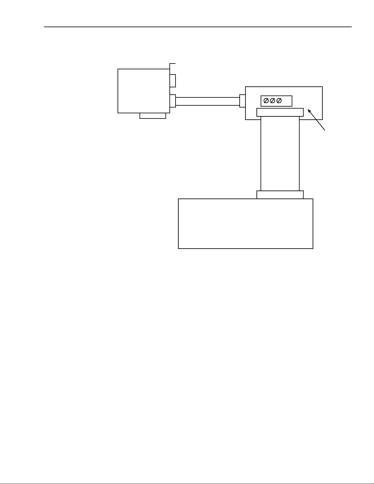
KPCI-3108 Series User’s Manual lnstallation 3-25
Figure 3-12
Connecting digital I/O accessories and an STA-3108-D1 accessory
Analog
KPCI-3108
Digital
CAB-1284CC
CAB-SSR, CACC-2000,
or ADP-5037 cable
(See Table 3-10 for
a correct match.)
PB-24, PB-24SM, ERB-24,
SSIO-24, SRA-01, or ERA-01
STA-3108-D1
50-pin Header
PIO-SSR
compatible
Page 82

3-26 lnstallation KPCI-3108 Series User’s Manual
Table 3-9
Digital I/O accessories and required connection accessories
Digital I/O accessories and required
adapter/screw-terminal accessory
PB-24 Industry-standard baseboard that accom-
modates 24 standard-size solid-state relay
modules.
PB-24SM Industry-standard baseboard that accom-
modates 24 miniature SM Series solid-state
relay modules.
SSIO-24 Module interface board that accommodates
up to 24 miniature, optically-isolated solidstate digital I/O modules
ERB-24 Relay board with 24 double-pole, double-
Digital I/O
SRA-01 Module interface board, in box, that
ERA-01 Relay board, in box, with eight single-pole,
STA-3108-D1 Adapter/screw-terminal accessory.
Adapter/screw-terminal
throw (dual Form C) electromechanical
relays
accommodates up to eight industrystandard solid-state digital I/O modules
double-throw (Form C) electromechanical
relays
Interfaces the “Digital” KPCI-3108 Series
I/O connector to a PB-24, PB-24SM,
ERB-24, SSIO-24, SRA-01, or ERA-01
digital I/O accessory, as well as to screwterminals that are numbered identically to
the “Digital” connector pins.
Required cables (in addition to
CAB-1284CC Series)
CAB-SSR Ribbon cable, 3 ft, that
connects PB-24 or
PB-24SM to a 50-pin
header
CACC-2000 Ribbon cable, 24 in,
with 50-pin female
connector on each end
ADP-5037 Conversion cable with
a 50-pin connector at
one end and a small
box, terminating in a
37-pin D-type
connector, at the other
end
CAB-1284CC
Series
IEEE 1284 type CC
cable; 36-pin miniCentronics connectors
on each end
Additional
required
accessoriesAccessory Description Cable Description
STA-3108-D1
accessory
STA-3108-D1
accessory
STA-3108-D1
accessory
None
Page 83

KPCI-3108 Series User’s Manual lnstallation 3-27
Table 3-10
Pin-to-pin correspondence between lower “Digital” I/O connector
and 50-pin accessory
At KPCI-3108 “Digital” I/O connector At STA-3108-D1 50-pin header
Assignment (Refer
also to Table 3-2 for
Pin number
1
2
3
4
5
6
7
8
9
10
11
12
13
14
15
16
17
18
19
20
21
22
23
24
25
26
27
28
29
30
31
32
33
34
35
36
I/O descriptions) Pin number Assignment
Bit 0
Bit 1
Bit 2
Bit 3
Bit 4
Bit 5
Bit 6
Bit 7
Bit 8
Bit 9
Bit 10
Bit 11
Bit 12
Bit 13
Bit 14
Bit 15
DGND
DGND
Bit 16
Bit 17
Bit 18
Bit 19
Bit 20
Bit 21
Bit 22
Bit 23
Bit 24
Bit 25
Bit 26
Bit 27
Bit 28
Bit 29
Bit 30
Bit 31
+5V
+5V
15
13
11
9
7
5
3
1
47
45
43
41
39
37
35
33
All even- numbered
pins
31
29
27
25
23
21
19
17
49 +5V
PA 0
PA 1
PA 2
PA 3
PA 4
PA 5
PA 6
PA 7
PB0
PB1
PB2
PB3
PB4
PB5
PB6
PB7
Digital common
Digital common
PC0
PC1
PC2
PC3
PC4
PC5
PC6
PC7
Page 84
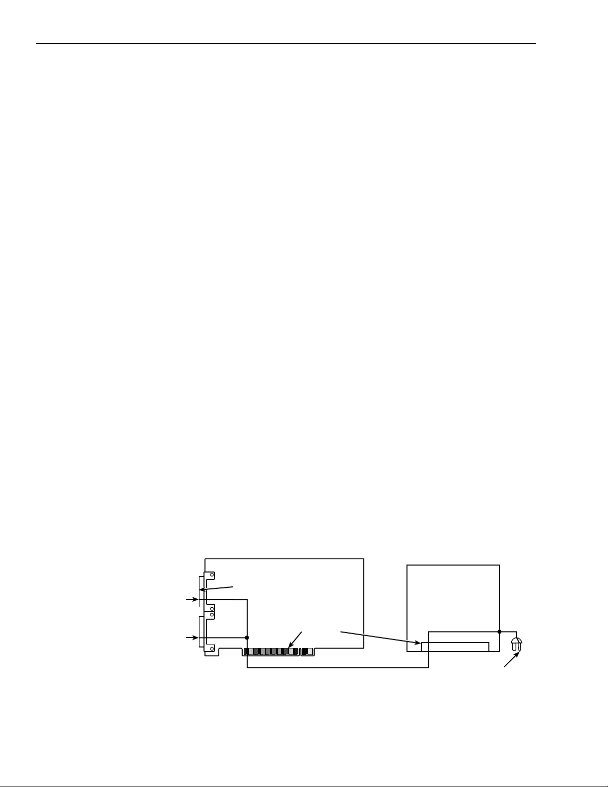
3-28 lnstallation KPCI-3108 Series User’s Manual
Wiring analog input signals
This section provides general guidance on wiring your circuits to single-ended and differential
inputs, as well as special precautions to avoid problems when wiring signals to a KPCI-3108 set
for high gains.
WARNING Do NOT connect data acquisition inputs to the AC line. Keep data
acquisition cables and connections away from any AC line connections. Interconnections or shorting between data and power lines can
result in personal injury or death or extensive damage to your computer. To prevent this problem, do the following:
• Avoid direct connections to the AC line by using safety approved
isolation transformers, isolation amplifiers, or both.
• Ensure that all connections are tight and sound, so that signal
wires are unlikely to come loose and short to hazardous voltages.
CAUTION Ensure that both the computer and the external circuits are turned
OFF before making any connections. Making connections while the
computer and external circuits are powered can damage the computer, the board, and the external circuit.
Ensure that no analog-input signal exceeds ±15V, which is the maximum allowable rating for the board. Exceeding ±15V will damage
the board.
NOTE KPCI-3108 boards contain separate ground connections for analo g and
digital signals. Use the analog ground (AGND) for analog signals and
analog power; use the digital ground (DGND) for digital signals and
other power-supply returns. Do this to avoid interference from digital
switching noise currents on sensitive analog signals. Howe ver, be aware
that both analog and digital grounds are tied together at the board PCI
connector and are ultimately connected to the building system ground
via the mains. See Figure 3-13. I/O connector pin assignments and
descriptions for AGND and DGND are provided in Figure 3-2, Figure
3-3, Table 3-1, and Table 3-2.
Figure 3-13
Analog and digital ground path
KPCI-3108 Board
I/O Connector
AGND
PCI Connector
DGND
Host Computer
To Mains
Page 85

KPCI-3108 Series User’s Manual lnstallation 3-29
NOTE Though the circuit diagrams show direct connections to channel input
pins of the main I/O connector, you must make actual connections
through the corresponding screw terminals of an STP-36 Series accessory or through EXP-1800 or MB Series expansion/signal-conditioning
accessories and unshared terminals of the required STA-3108-A Series
accessory.
The circuit diagrams in this section represent wiring of a single signal source to a single channel
(typically designated as “channel n”). Differential analog circuits can be used with any differential input. Single-ended analog circuits can be used with any single-ended input.
Wiring a signal to a single-ended analog input
NOTE Before wiring your signals to single-ended inputs, ensure that you
understand the limitations of single-ended inputs. Refer to Section 2,
“Choosing between the differential and single-ended termination
modes.”
Figure 3-14 shows the connections between a signal source and one channel of a KPCI-3108
board configured for single-ended input mode.
Figure 3-14
Wiring a signal source to a board configured for single-ended inputs
Signal
Source
+
-
Channel
AGND
n
High
KPCI-3108 Board
Wiring a floating signal source to a differential analog input
NOTE If you are unclear about whether to use differential or single-ended
input mode, refer to Section 2, “Choosing between the differential and
single-ended termination modes.”
Figure 3-15 shows three connection schemes for wiring a signal source to a KPCI-3108 channel
when the board is configured for differential input and the input signal source is floating.
Floating signal sources are ideally either totally ungrounded (a battery, for example) or are otherwise not connected either directly or indirectly to the building ground or analog signal ground.
(Real floating signal sources do have finite, though small, coupling to ground due to finite insulation resistance and other sources of current leakage, such as capacitive coupling in a transformer.) Examples of floating signal sources include devices powered by batteries, devices
powered through isolation transformers, ungrounded thermocouples, and outputs of isolation
amplifiers. Using floating signal source intrinsically avoids ground loops.
Page 86

3-30 lnstallation KPCI-3108 Series User’s Manual
However, when your KPCI-3108 board is used in the differential input mode, a current path
must be connected to the analog ground terminal. When the signal source floats, the lack of a
ground reference point allows instrumentation amplifier bias currents to raise the common-mode
voltage of the signal to high values. Excessive common mode voltages result in excessive signal
errors or, worse, amplifier saturation and unusable data.
NOTE The bias current of the input instrumentation amplifier is a very small
but finite current drawn from an input terminal to the amplifier. The
magnitude of the bias current depends on the amplifier design and may
range from a few femtoamperes to a few microamperes.
The common-mode voltage (Vcm) is a voltage that is common to both
the input-high and input-low terminals of a differential input: it appears
between each terminal and ground.
If your signal source is floating, you must provide the path to the analog ground. Use one or two
bias return resistors, as discussed below and illustrated in Figure 3-15.
Figure 3-15
Wiring a floating signal source to differential inputs: three common examples
R
s
Signal
Source
Signal
Source
+
-
R
Where > 100Ω
R
Where < 100Ω
R
R
+
s
+
-
R
s
R
s
Bridge
-
R
= 10,000 but ≤ 100MΩ
b
= 0Ω to 10,000
b
v
R
s
DC
Supply
Channel
Channel n Low
R
b
s
Channel
Channel
R
b
R
s
Channel
Channel
Where is a variable resistor for
R
v
balancing the bridge
n
High
R
b
AGND
n
High
n
Low
AGND
n
High
n
Low
AGND
KPCI-3108 Board
KPCI-3108 Board
KPCI-3108 Board
Page 87

KPCI-3108 Series User’s Manual lnstallation 3-31
The minimum bias return resistance and the number of bias resistors (one or two) are determined by noise considerations. The maximum bias return resistance (Rb) is limited by the maximum acceptable common-mode voltage that occurs due to the bias current, as follows:
Common-mode voltage due to bias current = (Bias current) * (Bias return resistance, Rb)
The remaining discussions of this section guide you in selecting bias return resistors.
Using a single bias return resistor (middle circuit of Figure 3-15). If the signal source resis-
tance (RS) is low, one bias return resistor connected between the input-low terminal and the analog ground is adequate.
The minimum bias return resistance is determined by the signal source resistance and the susceptibility and exposure of your circuit to noise pickup from the environment. If the source resistance (RS) is low, the bias resistance can generally be low. In some cases, the bias resistance (Rb)
can be zero. That is, you can connect a lead directly between the analog ground and the negative
terminal of the signal source. However, the following then occurs:
• Electrostatically-coupled noise in the negative signal lead is shunted directly to ground and
does not affect the negative signal input.
• Electrostatically-coupled noise in the positive signal lead is not shunted directly to ground
and causes a net noise voltage at the positive signal input.
The net voltage at the positive signal input cannot be rejected by the common-mode rejection
capabilities of the KPCI-3108.
Therefore, depending on the source resistance (R
) and/or the electrostatic noise pickup, it is
S
frequently better to use a larger bias resistance (Rb) to help balance the ground return paths of
the positive and negative signals. The higher resistance makes the ground paths and noise coupling in the positive and negative signals more similar. The noise that is common to both positive
and negative signals can then be rejected as part of the common mode voltage. If the source
resistance is less than 100 ohms, you may select the bias return resistance as follows:
Bias return resistance, R
= 10,000 * (Source resistance, RS) if R
b
< 100Ω
S
Using two bias return resistors (top circuit of Figure 3-15). You can slightly improve noise
rejection by connecting identical bias return resistors to both the positive and negative signals.
This balances the ground return paths. Use the following resistance value:
Bias return resistance, R
= 10,000 * (Source resistance, R
b
), 100MΩ max, if RS > 100Ω
S
However, be aware that the bias return resistor connected to the input-high terminal loads the
signal, causing a proportional error.
Using no bias return resistors with a bridge circuit (bottom circuit of Figure 3-15). In the
lower circuit of Figure 3-15, added bias return resistors are not needed. The bridge resistors at
the signal source inherently provide the bias current return path. The common mode voltage at
the input terminals is the voltage drop across RS of the bridge.
Wiring a ground-referenced signal source to a differential analog input
NOTE If you are unclear about whether to use differential or single-ended
input mode, refer to Section 2, “Choosing between the differential and
single-ended termination modes.”
A ground-referenced signal source is a signal source that is connected directly or indirectly to
the building system ground. The analog signal ground of the KPCI-3108 is ultimately connected
to the building system ground via the power mains, as shown in Figure 3-13. Therefore, the
ground-referenced signal source is also indirectly connected to the analog ground.
Page 88

3-32 lnstallation KPCI-3108 Series User’s Manual
However, the quality of the ground connection between the signal source and analog ground of
the KPCI-3108 may be poor. The signal-source ground and the KPCI-3108 board analog ground
are typically not at the same voltage level. This voltage difference is due to the wiring between
the data acquisition equipment and the building system ground, to which power-using and noisegenerating equipment is typically also connected. The voltage difference is seen at the KPCI3108 differential input terminals as a common-mode voltage (Vcm), so called because it is effectively common to both the input-high and input-low terminals. An ideal, properly connected differential input responds only to the difference in the signals at the input-high and input-low
terminals. The common-mode voltage is rejected, leaving only the desired signal. Practically, the
common-mode voltage always causes an error, typically small, that is limited by the commonmode rejection ratio (CMRR) of the differential input.
Figure 3-16 illustrates how to satisfactorily connect a ground-referenced signal source to a differential input. In the upper circuit of Figure 3-16, a separate ground return line is connected
between the negative-terminal ground of the signal source and the analog ground of the
KPCI-1800HC Series board. Because both the input-high and input-low terminals of the
KPCI-1800HC have high input impedance, effectively all ground currents due to ground voltages flow through the separate ground-return line. Because the separate ground return line is
common to both the input-high and input-low terminals, the voltage drop across it is rejected as
a common-mode voltage.
In the lower circuit of Figure 3-16, the grounding connection for a bridge circuit powered by a
ground-referenced power supply is the same as for a floating bridge. When the bridge has a
ground-referenced power supply, the common mode voltage is the sum of the voltage drop
across the ground line and the voltage drop across RS of the bridge.
Figure 3-16
Satisfactory differential input connections that avoid a ground loop
with ground-referenced signals
R
Signal
Source
Signal Source
V
Ground
g1
R
v
R
s
+
+
-
s
E
s
Bridge
-
V
cm
Channel
Channel
R
V
cm
wire
V
= -
g1
n
High
E
Low
AGND
s
AGND
V
g2
n
Low
n
V
g2
Channel n High
Channel
KPCI-3108 Board
Do not join Low
to AGND at the
computer
KPCI-3108 Board
DC
Supply
(Internally
ground-coupled)
Where is a variable resistor for
R
balancing the bridge
v
Page 89

KPCI-3108 Series User’s Manual lnstallation 3-33
Figure 3-17 illustrates how NOT to connect a differential input. If the analog ground and inputlow terminal of the KPCI-3108 board are joined near the board, a ground loop current flows in
the negative signal lead. The voltage difference across this signal lead is then a component of the
measured signal, not a common-mode voltage. A differential amplifier cannot reject this
unwanted signal component.
Figure 3-17
Improper differential input connection, which creates a ground loop error
R
Signal
Source
Signal Source
Ground
+
-
V
g1
s
E
s
Channel
Channel
V
R
V
cm
wire
cm
n
V
= -
g1
n
High
Low
V
g2
+
E
V
s
AGND
V
g2
cm
KPCI-3108 Board
NOTE
This diagram is included
only to illustrate an
incorrectly wired input; do
not use this configuration.
Avoiding wiring problems at high gains
Operating a KPCI-3108 board at a gain of 200 or more can lead to problems if your application
is unable to cope with noise. If special precautions are not taken, the high gain, high speed, and
large bandwidth of this board allow thermal emfs and noise to easily degrade performance. The
following suggestions are provided to help you to minimize problems at high gain.
• Connect low-level signals to inputs configured as differential inputs. Inputting signals at high
gains in single-ended mode introduces enough ground-loop noise to produce large fluctuations in readings.
• Minimize noise from crosstalk and induced-voltage pickup in cables and screw-terminal
accessories. Use shielded cables for low level signals whenever possible. Induced noise from
radio frequency (RF) and magnetic fields can easily exceed tens of microvolts, even on onefoot or two-foot long cables. Shielded cable helps to avoid this problem.The CAB-1284CC
Series cables (or standard IEEE 1284 Type C-C mini-Centronics cables) that are used to connect accessories directly to KPCI-3108 I/O connectors are shielded, and signals to differential inputs are conducted through twisted pairs. Nonetheless, minimize the length of
CAB-1284CC Series cables to minimize interferences.Connect cable shields to the analog
ground (AGND) and the inner conductors to the input low (LO) and input-high (HI) terminals. Channel LO and AGND should have a common DC return (or connection) at some
point; this return should be as close to the signal source as possible.
• Avoid bimetallic junctions in the input circuitry. For example, the thermal emf of a Kovar-to-
copper junction, such as at the Kovar leads of reed relay, is typically 40µV/˚C. Thermal emfs
at bimetallic junctions, combined with air currents and other sources of temperature variation, can introduce strange random signal variations.
• Consider filtering, which can be accomplished with hardware (resistors, capacitors, and so
on) but is often accomplished more easily with software. Instead of reading the channel
once, read it 10 or more times in quick succession and average the readings. If the noise is
random and Gaussian, it will be reduced by the square root of the number of readings.
Refer also to Section 2, “Optimizing throughput,” for additional precautions about assigning
high gains to channels in the channel-gain queue.
Page 90

3-34 lnstallation KPCI-3108 Series User’s Manual
Wiring analog output signals (KPCI-3108 board only)
This section provides a few guidelines on wiring the analog outputs from the two 16-bit DACs
(digital-to-analog converters) that are available on a KPCI-3108 board. Each DAC can be software-configured to output a range of ±10V, ±5V, 0 to 10V, or 0 to 5V. Performance characteristics and drive capabilities for these DACs are listed in Appendix A.
WARNING Do NOT intersperse data acquisition connections with AC line con-
nections. Keep data acquisition cables and connections away from
any AC line connections. Interconnections or shorting between data
and power lines can result in personal injury or death or extensive
damage to your computer. To prevent this problem, ensure that all
connections are tight and sound, so that signal wires are unlikely to
come loose and short to hazardous voltages.
CAUTION Ensure that both the computer and the external circuit are turned
OFF before making any connections. Making connections while the
computer and external circuits are powered can damage the computer, the board, and the external circuit.
Ensure that connected loads do not draw more than 5 mA, the maximum allowable output current for the board.
NOTE Avoid large capacitive loads at the analog outputs. Capacitive loads
higher than 100µF destabilize the analog outputs and make them susceptible to ringing (transient oscillations).
KPCI-3108 boards contain separate ground connections for analog and
digital signals. Use the analog ground (AGND) for analog signals and
analog power; use the digital ground (DGND) for digital signals and
other power-supply returns. Do this to avoid interference from digital
switching noise currents on sensitive analog signals. Howe ver, be aware
that both analog and digital grounds are tied together at the board PCI
connector and are ultimately connected to the building system ground
via the mains. See Figure 3-18. I/O connector pin assignments and
descriptions for AGND and DGND are provided in Figure 3-2,
Figure 3-3, Table 3-1, and Table 3-2.
Figure 3-18
Analog and digital ground path
KPCI-3108 Board
I/O Connector
AGND
PCI Connector
DGND
Host Computer
To Mains
Page 91

KPCI-3108 Series User’s Manual lnstallation 3-35
You must make all analog output connections to the upper “Analog” I/O connector of the board
through one of the following:
• The screw terminals of an STP-36 screw terminal accessory. To connect an STP-36 acces-
sory to your board, refer to “Connecting an STP-36 screw terminal accessory to a KPCI3108 board” earlier in Section 3.
• Terminals on an MB-02 signal-conditioning/channel-expansion accessory and unshared ter-
minals of the required STA-3108-A Series accessory. Refer to the manual for your MB-02
Series accessory and to “Connecting an MB-02 signal conditioning/channel-expansion
accessory to the KPCI-3108 board via an STA-3108-A3 accessory” earlier in Section 3.
The appropriate STP-36 or STA-3108-A3 screw terminals are identified in
Table 3-11.
Table 3-11
Screw terminals used to wire analog outputs of KPC-3108 board
Screw
terminal Assignment Description
17, 18 AGND Analog ground
35 DAC1 Output Analog output from digital-to-analog converter number 1*
36 DAC0 Output Analog output from digital-to-analog converter number 0*
Wiring digital input and output signals
WARNING Do NOT connect data acquisition inputs to the AC line. Keep data
acquisition cables and connections away from any AC line connections. Interconnections or shorting between data and power lines can
result in personal injury or death or extensive damage to your computer. To prevent this problem, do the following:
• Avoid direct connections to the AC line by using safety approved
isolation transformers, isolation amplifiers, or both.
• Ensure that all connections are tight and sound, so that signal
wires are unlikely to come loose and short to hazardous voltages.
CAUTION Ensure that both the computer and the external circuit are turned
OFF before making any connections. Making connections while the
computer and external circuits are powered can damage the computer, the board, and the external circuit.
NOTE KPCI-3108 boards contain separate ground connections for analo g and
digital signals. Use the analog ground (AGND) for analog signals and
analog power; use the digital ground (DGND) for digital signals and
other power-supply returns. Do this to avoid interference from digital
switching noise currents on sensitive analog signals. Howe ver, be aware
that both analog and digital grounds are tied together at the board PCI
connector and are ultimately connected to the building system ground
via the mains. See Figure 3-19. I/O connector pin assignments and
descriptions for AGND and DGND are provided in Figure 3-2,
Figure 3-3, Table 3-1, and Table 3-2.
Page 92

3-36 lnstallation KPCI-3108 Series User’s Manual
Figure 3-19
Analog and digital ground path
KPCI-3108 Board
I/O Connector
AGND
PCI Connector
DGND
Host Computer
To Mains
A KPCI-3108 board has two types of digital I/O. The lower “Digital” I/O connector provides 32
high current general-purpose bits. The upper “Analog” I/O connector provides twelve multifunction TTL bits. Following “General wiring considerations for digital I/O,” these two types of
digital I/O are discussed separately below.
General wiring considerations for digital I/O
For all digital I/O, logic 1 on an I/O line indicates that the input/output is high (greater than
2.0V); logic 0 on an I/O line indicates that the input/output is low (less than 0.8V). The digital
inputs are compatible with TTL-level signals.
External circuits must properly match the input requirements of the board. Some applications
may require you to eliminate contact bounce at the input. The effects of contact bounce may be
eliminated by programming in your application software. However, it is often desirable to eliminate contact bounce from the signal, using a de-bounce circuit between the contacts and the
KPCI-3108 input. Figure 3-20 shows a typical de-bounce circuit that can be used with Form C
contacts.
Figure 3-20
Contact de-bounce circuit
+5V
10kΩ 10kΩ
Digital
Common
GND
Compatible
AND Gate
To Digital Input of a
KPCI-3108 Board
TTL
Page 93

KPCI-3108 Series User’s Manual lnstallation 3-37
Wiring general-purpose digital I/O signals
The lower “Digital” I/0 connector provides 32 bits of high current I/O (15 mA max. source, 64
mA max. sink output current). These general-purpose bits are software-configurable as either
inputs or outputs in groups of eight—each group of eight bits being handled by one of four
eight-bit registers. These bits may be used for a variety of purposes, as for the bits of common
digital I/O boards such as the Keithley PIO-24 and KPCI-PIO24 boards. The output current
capabilities of these bits are much higher than available from the industry-standard type-8255
digital I/O chip on many commercial digital I/O boards.
NOTE No pull-up resistor is provided on these lines. If used as an input for a
contact closure or similar signal, a pull-up resistor will need to be
included in your circuitry.
Wire a general-purpose digital I/O signal between the appropriate digital I/O pin and a digital
ground pin on your KPCI-3108 board. Make all connections to the lower “Digital” I/O connector of the board through one of the following:
• Connect all I/O through the screw terminals of an STP-36 screw terminal accessory. Refer to
“Connecting an STP-36 screw terminal accessory to a KPC-3108 board.
• Terminals on any of six compatible digital I/O accessories and unshared terminals of the
required STA-3108-D1 accessory. Refer to the manual for your digital I/O accessory and to
“Connecting digital I/O accessories to the KPCI-3108 board via an STA-3108-D1 accessory” earlier in Section 3.
The appropriate STP-36, or STA-3108-D1 screw terminals are identified in
Table 3-12.
Table 3-12
Screw terminals used to wire general-purpose digital I/O
Screw
terminal Assignment Description
1
2
3
:
8
9
10
11
:
16
17, 18 DGND Digital grounds.
19
20
21
:
26
27
28
29
:
34
35, 36 +5V + 5 VDC from computer bus. (Refer to “Wiring +5V power to
Bit 0
Bit 1
Bit 2
:
Bit 7
Bit 8
Bit 9
Bit 10
:
Bit 15
Bit 16
Bit 17
Bit 18
:
Bit 23
Bit 24
Bit 25
Bit 26
:
Bit 31
General-purpose digital I/O bits, channel 0. As a group, these 8 bits
are user-configurable as either all inputs or all outputs. (The 8 bits
comprise the register of a type 652 chip.)
General-purpose digital I/O bits, channel 1. As a group, these 8 bits
are user-configurable as either all inputs or all outputs. (The 8 bits
comprise the register of a type 652 chip.)
General-purpose digital I/O bits, channel 2. As a group, these 8 bits
are user-configurable as either all inputs or all outputs. (The 8 bits
comprise the register of a type 652 chip.)
General-purpose digital I/O bits, channel 3. As a group, these 8 bits
are user-configurable as either all inputs or all outputs. (The 8 bits
comprise the register of a type 652 chip.)
external circuits.”)
Page 94

3-38 lnstallation KPCI-3108 Series User’s Manual
Wiring multi-function digital I/O signals
KPCI-3108 boards provide six digital inputs and six digital outputs at the upper “Analog” I/O
connector. These I/O bits are software-configurable to preform a variety of functions, including
control of external signal conditioning and expansion accessories.
NOTE Inputs IP0-IP5 include a 10kΩ pull-up resistor on the board.
You must wire all multi-function digital I/O connections to the upper “Analog” I/O connector of
the board through one of the following:
• The screw terminals of an STP-36 screw terminal accessory. Wire a multi-function I/O signal
between the appropriate digital I/O terminal and a digital ground terminal. To connect an
STP-36 accessory to your board, refer to “Connecting an STP-36 screw terminal accessory
to a KPCI-3108 board” earlier in Section 3.
• Unshared digital I/O screw terminals of the required STA-3108-A Series accessory, when
using an analog signal-conditioning/expansion accessory. Refer to the manual for your
signal-conditioning/expansion accessory and to one of the following sections earlier in
Section 3:
– “Connecting EXP-1800 channel-expansion accessories to the KPCI-3108 board via an
STA-3108-A1 accessory”
– “Connecting an MB-01, MB-05, or STA-MB signal conditioning accessory to the
KPCI-3108 board via an STA-3108-A2 accessory”
– “Connecting an MB-02 signal conditioning/channel-expansion accessory to the KPCI-3108
board via an STA-3108-A3 accessory”
Table 3-13 summarizes general STP-36 or STA-3108-A Series screw terminals used to wire the
multi-function digital I/O of the KPC-3108 board. The assignments are ordered numerically
according to the identically-numbered pins of a KPCI-3108 upper “Analog” I/O connector.
Table 3-13
Assignments and descriptions for multi-function digital I/O accessories
Screw
terminal Assignment Description
1
2
3
4
5
6
7 DGND Digital ground.
19
20
21
IP5
IP3
IP1
OP5
OP3
OP1
IP4
IP2
IP0
Multi-function digital input bits, user-configurable for:
• Counter/timer timebase or gate inputs
• External pacer input for A/D or D/A conversion
• External digital trigger
• Target-mode digital input
Multi-function digital output bits, user-configurable for:
• Counter/timer outputs
• Trigger output
• Control and/or addressing for EXP-1800 expansion accessories
or MB-02 signal conditioning accessories
• Pacer clock output
• Target-mode digital output
Multi-function digital input bits, user-configurable for:
• Counter/timer timebase or gate inputs
• External pacer for A/D or D/A conversion
• External digital trigger
• Target-mode digital input
Page 95

KPCI-3108 Series User’s Manual lnstallation 3-39
Table 3-13 (cont.)
Assignments and descriptions for multi-function digital I/O accessories
Screw
terminal Assignment Description
22
23
24
25 +5 V +5 VDC from computer bus. (Refer to “Wiring +5V power to
Table 3-14 summarizes specific pin/terminal assignments and descriptions for the multifunctional digital inputs at screw terminals of STP-36 and STA-3108-A Series accessories. The
assignments are ordered numerically according to the assigned bits.
OP4
OP2
OP0
Multi-function digital output bits, user-configurable for:
• Counter/timer outputs
• Trigger output
• Control and/or addressing for EXP-1800 expansion accessories
or MB-02 signal conditioning accessories
• Pacer clock output
• Target-mode digital output
external circuits.”)
Table 3-14
Bit assignments and descriptions for multi-function digital inputs
Bit assignment Screw terminal Description
IP0 21 Configurable as one of the following:
• XPCLK, external pacer clock input
• General-purpose input bit, target mode
IP1 3 Configurable as one of the following:
• TGIN, external trigger or gate input
• General-purpose input bit, target mode
IP2 20 Configurable as one of the following:
• Counter/timer C/T0 external clock input
• General-purpose input bit, target mode
IP3 2 Configurable as one of the following:
• Counter/timer C/T1 external clock input
• General-purpose input bit, target mode
IP4 19 Configurable as one of the following:
• Counter/timer C/T0 external gate input
• General-purpose input bit, target mode
IP5 1 Configurable as one of the following:
• Counter/timer C/T1 external gate input
• General-purpose input bit, target mode
Page 96

3-40 lnstallation KPCI-3108 Series User’s Manual
At the multi-functional digital output terminals, three user-selectable options provide three different combinations of available functions. Table 3-15 summarizes specific bit assignments and
descriptions for multi-function digital outputs at screw terminals of STP-36 and STA-3108-A
Series accessories.
Table 3-15
Bit assignments and descriptions for multi-function digital outputs
Output
mode Bit assignment Screw terminal Description
0 OP0 24 General-purpose output bit, target-mode
OP1 6 General-purpose output bit, target-mode
OP2 23 General-purpose output bit, target-mode
OP3 5 General-purpose output bit, target-mode
OP4 22 General-purpose output bit, target-mode
OP5 4 Configurable as one of the following:
• TGOUT (trigger-out output)
• Pacer clock output
• Counter/timer C/T0, CT1, or CT2 output
1 OP0 24 Frame sync
OP1 6 Counter/timer C/T0 output
OP2 23 Counter/timer C/T1 output
OP3 5 Counter/timer C/T2 output
OP4 22 Pacer-clock output
OP5 4 Configurable as one of the following:
• TGOUT (trigger-out) output
• Pacer clock output
• Counter/timer C/T0, CT1, or CT2 output
2 OP0 24 External address bit 0 for multiplexing of expansion-accessory channels
OP1 6 External address bit 1 for multiplexing of expansion-accessory channels
OP2 23 External address bit 2 for multiplexing of expansion-accessory channels
OP3 5 External address bit 3 for multiplexing of expansion-accessory channels
OP4 22 External gain bit for some expansion accessories (e.g. EXP-1800)
OP5 4 Configurable as one of the following:
• TGOUT (trigger-out output)
• Pacer clock output
• Counter/timer C/T0, CT1, or CT2 output
Page 97

KPCI-3108 Series User’s Manual lnstallation 3-41
More information about the configurable functions of the multi-function digital I/O is available
as follows:
• The external pacer clock input function (XPCLK) is described in Section 2 in the following
sections: “Pacer clock sources,” “The external pacer clock (XPCLK) digital input function,”
and, in context, “Triggers” and “Gates.”
• The external trigger or gate input function is described in Section 2 under “Triggers,”
“Gates,” and “The trigger in (TGIN) digital input function.” Use of a trigger input signal
(TGIN) for multiple-board synchronization is described, in context, in the next section,
“Synchronizing multiple boards.”
• The trigger output function (TGOUT) is described in Section 2 under “The trigger-out
(TGOUT) digital output function” and, in context, in the next section, “Synchronizing multiple boards.”
• The pacer clock output is discussed briefly in Section 2 under “The pacer-clock output
function.”
• Information about the use of address and/or synchronization bits for expansion/signal condi-
tioning-accessories (e.g. for EXP-1800, MB-02) is provided in the instructions that accompany those accessories.
• The nature and use of counter/timer inputs and outputs is discussed in Section 2 under
“Counter/timer features” and “The counter/timer digital output functions.”
• The nature and use of the multi-function digital I/O for target-mode data transfer is discussed
in your DriverLINX documentation.
Wiring counter/timer signals
The multi-function digital I/O bits, after appropriate configuration, are used for all counter/timer
inputs and outputs. For information about wiring to these bits, refer to the subsection preceeding, “Wiring multi-function digital I/O signals.”
Page 98

3-42 lnstallation KPCI-3108 Series User’s Manual
Synchronizing multiple boards
You can synchronize up to three KPCI-3108 boards using trigger and gate signals from the main
I/O connectors. A/D (analog-to-digital) conversions at synchronized boards can be started simultaneously by a single event, regardless of whether the boards have been programmed for the
same conversion rate or for different conversion rates.
The onboard pacer clock of each board is designed to be tightly coupled with trigger or gate
events. Within a short, defined time lag, each synchronized board begins the first analog conversion when the board receives a trigger or gate signal. (Refer to “Triggers” and “Gates” in
Section 2). Each board then continues analog conversions at the rate previously set for that board
via DriverLINX.
Figure 3-21 shows two connection schemes for synchronizing multiple boards. In both schemes,
the conversion rate for each board is timed by the internal pacer clock for that board. When making terminal connections, refer to the preceeding subsection, “Wiring multi-function digital I/O
signals.”
Figure 3-21
Two connection schemes for synchronizing multiple boards
Board 0
Rate a
Board 1
Rate b
Board 2
Rate c
TGIN
TGIN
TGIN
a. Scheme 1
Trigger or
Gate
Board 0
Rate a
Board 1
Rate b
Board 2
Rate c
b. Scheme 2
TGIN
TGOUT
TGIN
TGIN
Trigger or
Gate
(optional)
Board synchronization scheme 1
In Scheme 1, start conversions at synchronized boards with one external trigger/gate signal.
Connect the trigger/gate inputs of the boards together such that each board receives the trigger or
gate input simultaneously.
A/D conversions at each board start 400 ±100ns after the active edge of a trigger or gate input.
Therefore, boards can be synchronized within 100 ±100ns. For example, one board could start
conversions as soon as 300ns after the active edge of the trigger input, while another board could
start conversions as late as 500ns after the active edge of the trigger input.
When using scheme 1, you can time subsequent A/D conversions using either the onboard pacer
clock or an external pacer clock.
Page 99

KPCI-3108 Series User’s Manual lnstallation 3-43
Board synchronization scheme 2
In Scheme 2, start conversions in either of two ways: by an external trigger/gate signal or by
software. The board connections are in a master/slave relationship; board 0 is the master, and the
other boards are the slaves.
If using a hardware trigger for board 0 of scheme 2, board 0 triggers conversions in all boards
immediately. Note that TGOUT is an active, high-going signal. Therefore, you must program the
TGIN input of each slave board to respond to the positive (rising) edge of the TGOUT signal.
If you use software to enable board 0, the following sequence occurs:
1. The board-0 pacer clock first triggers conversions in the slave boards.
2. Then, conversions start in board 0.
Conversions in board 0 are delayed by a protection feature, which is built into the register that
creates software-triggered conversions. This protection feature prevents false conversions.
Wiring +5V power to external circuits
CAUTION Ensure that both the computer and the external circuit are turned
OFF before making any connections. Making connections while the
computer and external circuits are powered can damage the computer, the board, and the external circuit.
Do not connect the +5V output pins to external power supplies.
Connecting the +5V output pins to external power supplies may
damage the external supplies, the board, and the computer.
Do not draw more than 1.0A, total, from all +5V output pins combined. Drawing more than 1.0A, total, may damage the board. Also,
keep in mind that the 5V output comes from the computer power
bus. Know the limits of the computer 5V power bus and the current
drawn from it by other boards and devices. Other demands on the
5V power bus may limit the current drawn from your board to less
than 1.0A.
NOTE KPCI-3108 boards contain separate ground connections for analo g and
digital signals. Use the analog ground (AGND) for analog signals and
analog power; use the digital ground (DGND) for digital signals and
other power-supply returns. Do this to avoid interference from digital
switching noise currents on sensitive analog signals. Howe ver, be aware
that both analog and digital grounds are tied together at the board PCI
connector and are ultimately connected to the building system ground
via the mains. See Figure 3-22. I/O connector pin assignments and
descriptions for AGND and DGND are provided in Figure 3-2,
Figure 3-3, Table 3-1, and Table 3-2.
Page 100
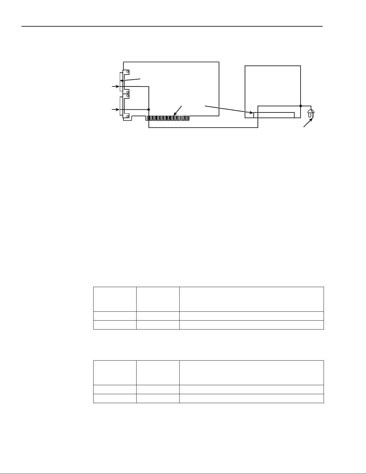
3-44 lnstallation KPCI-3108 Series User’s Manual
Figure 3-22
Analog and digital ground path
KPCI-3108 Board
I/O Connector
AGND
PCI Connector
DGND
Host Computer
To Mains
Power at +5V for light external circuits, such as pull-up resistors, may be drawn indirectly from
the host computer power bus via the KPCI-3108 I/O connectors. If you ensure that the following
conditions are maintained, this power may also be used to energize external accessories:
• The maximum total current drawn from the +5V pins on both I/O connectors combined —
pin 25 on the upper “Analog” connector and pins 35 and 36 on the lower “Digital” I/O
connector—must be less than 1.0A. The total current drawn to power the board and all
external circuits must not overload the computer power bus.
• The total current drawn to power the board and all external circuits must not overload the
computer power bus.
Power connections at the upper “Analog” I/O connector and at screw terminals of STP-36
and STA-3108-A Series accessories connected to it are listed in Table 3-16.
Power connections at the lower “Digital” I/O connector and at screw terminals of STP-36
and STA-3108-D1 accessories connected to it are listed in Table 3-17.
The +5V power is available at screw terminal accessories as listed.
Table 3-16
Power connections at the upper “Analog” I/O connector
Screw terminal
or “Analog”
connector pin Assignment Description
7 DGND Digital ground
25 +5 V +5 VDC from computer bus
Table 3-17
Power connections at the lower “Digital” I/O connector
Screw terminal
or “Digital”
connector pin Assignment Description
17, 18 DGND Digital grounds
35, 36 +5V +5 VDC from computer bus
 Loading...