

Page 1
PROTO Module
The PROTO Module is a prototyping board that enables users to design and interface
their own circuits to the Series 500. All Series 500 slot signals are available on the
PROTO Module including the supply voltages and grounds. The PROTO Module includes interface logic for one TTGcompatible B-bit bidirectional data port. This allows
&bit data transfers to and from the user-designed circuitry on the PROTO Module.
One byte of data can be written to or read from the PROTO Module using the slotdependent CMDA address.
Circuit Design Information
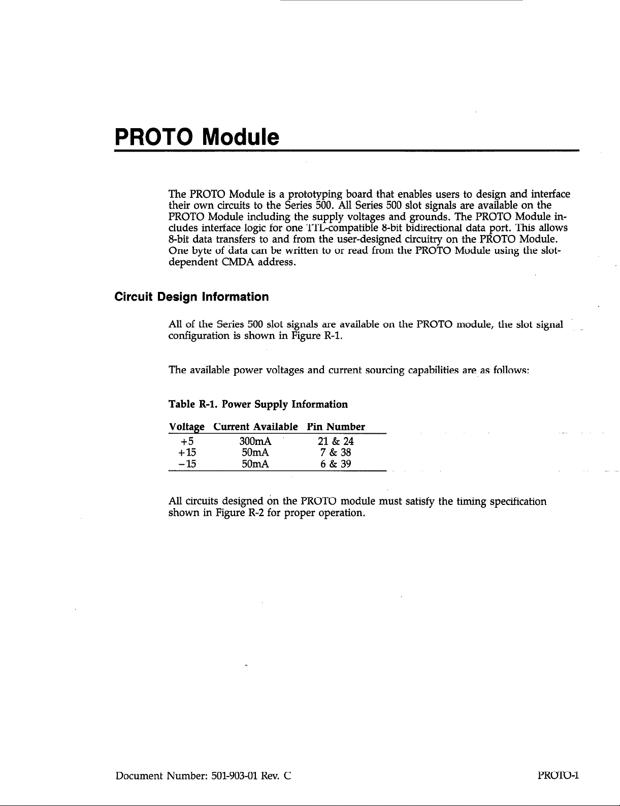
All of the Series 500 slot signals are available on the PROTO module, the slot signal
configuration is shown in Figure R-l.
The available power voltages and current sourcing capabilities are as follows:
Table R-l. Power Supply Information
Voltage Current Available Pin Number
+5 3oomA 21 & 24
+15 5omA 7 & 38
-15 5omA 6 & 39
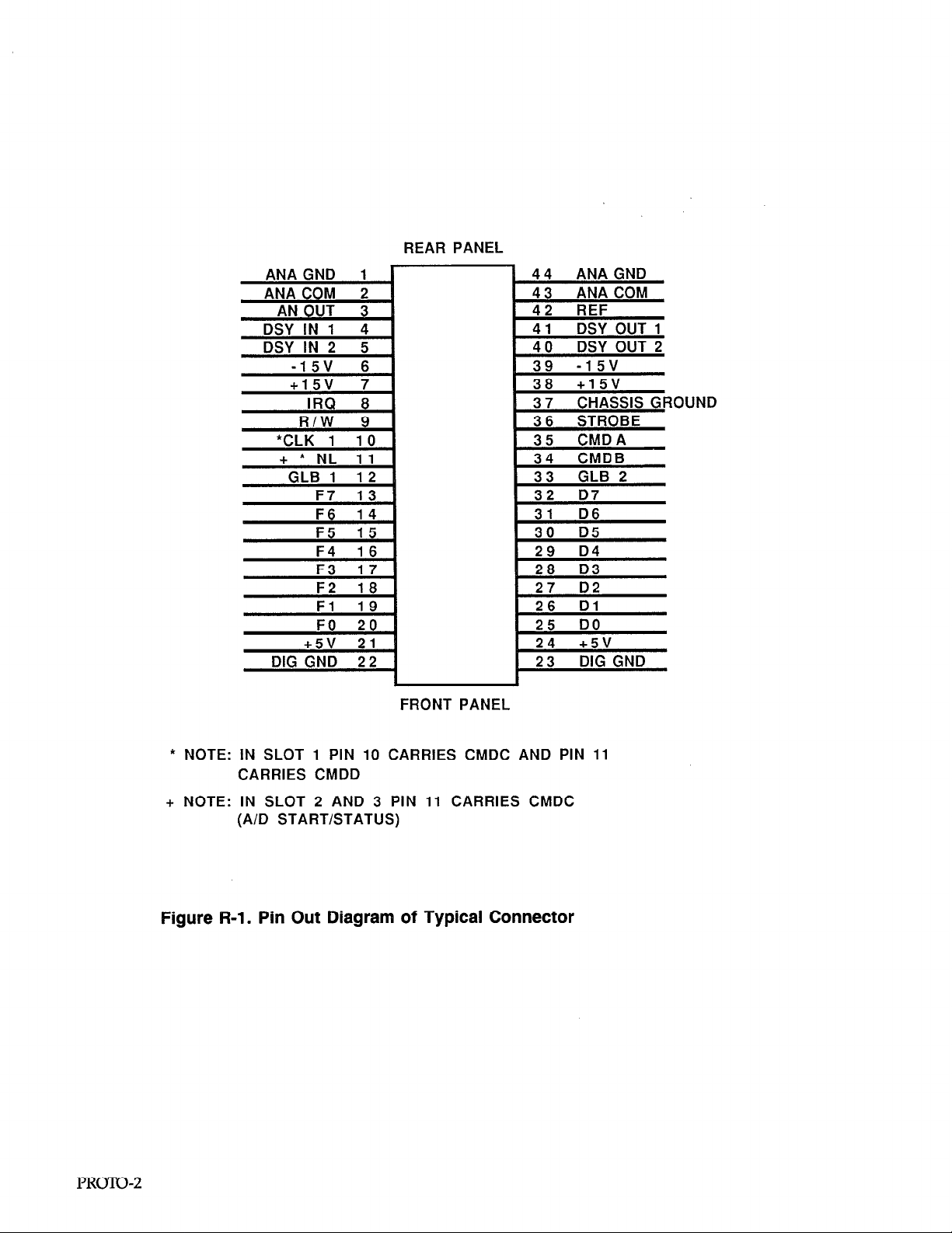
All circuits designed on the PROTO module must satisfy the timing specification
shown in Figure R-2 for proper operation.
Document Number: 501-903-01 Rev. C PROTo-
Page 2
REAR PANEL
ANA GND
ANA f’flllfi
ULC
F7 13 1
1
3
FRONT PANEL
ANA CAM
‘;LB 2
1 32 D7
PROTo-
* NOTE: IN SLOT 1 PIN 10 CARRIES CMDC AND PIN 11
CARRIES CMDD
+ NOTE: IN SLOT 2 AND 3 PIN 11 CARRIES CMDC
(A/D START/STATUS)
Figure R-l. Pin Out Diagram of Typical Connector
Page 3
READ CYCLE
‘CMDA
DATA
‘CMDA
DATA -<
15 w-4
DATA IS VALID FROM PC
b-@lt7
t1
M- t2
DATA MUST BE VALID
t4
-+l++l t3
I++1 16
R/W
* NOTE: THE TIMING FOR THE CMDB SIGNAL IS THE SAME AS CMDA
t1
t2
13
14
15
t6
t7
18
310n.s typ
200nS min
OnS min
310nS typ
5nS min
1OnS min
55nS min
IOnS min
>
l+---4t8
Figure R-2. Read/Write Timing Diagrams
Port Addressing
The read/write port on the PROTO module is accessed through the slot-dependent
CMDA signal. The CMDA addresses are shown in Table R-2.
PRCJTO-3
Page 4

Table R-2. Locations for Slot-Dependent CMDA
Slot IBM Location*
1 CFFSO
2 CFF82
3 CFF84
4 CFF86
CFF88
z
CFF8A
7 CFF8C
CFF8E
;
CFF90
10 CFF92
*Note: First character of address depends on address location of Series 500 card.
Following program examples assume interface is set to address CFF8.
188 DEFSEG=&HCFFB
2@3 CtlDA=&HE32
36161 POKE CMDHY &Htil
480 IIAL=PEEK < CtlI.M>
580 F’RIt4T HEXBCUAL>
Figure R-3. Proto Board Addressing
User Circuit Interfacing
The Series 500 slot includes a second command line, CMDB, which is identical in function to CMDA. If you wish to communicate throu h the CMDB line, you must
duplicate the circuitry already on the PROTO mo f ule for CMDA, and connect its control line to the CMDB pin (pin 34) on the PROTO module card edge connector rather
than the CMDA pin.
All digital circuit ground lines should be connected to DIG GND on the Series 500
slot. All analog circuit ground lines should be connected to ANA GND on the Series
500 slot.
The AN OUT signal line on the Series 500 slot routes an analog signal to slot 1 were it
may be digitized or multiplexed by another module. For example, if an analog signal is
present on a PROTO module which is in slot 5, the analog signal can be attached to
the AN OUT line on the Series 500 slot. With an AIM1 module in slot 1 (for multiplexing the analog signal to the A/D), and an ADMl in slot 2 (to preform the A/D conversion), the following program could be used to measure the voltage on the PROTO
module.
‘SET DATA SEGMENT TO SERIES 500 ADDRESS
‘PROTO BOARD IS IN SLOT 2
‘WRITE A 61 HEX TO THE PROTO BOARD PORT
‘READ A VALUE FROM THE PROTO BOARD PORT
‘PRINT THE VALUE READ IN HEX
PROT.O-4
Page 5

j.00
200
300
400
500
600
700
300
980
Gfi It.j=&H30
COt+JERT=&H98
L-~[.j4+32
HI GH=&H83
P’OKE SLOT 9 5
POKE C;AINr 0
POKE CONVERTI 0
1000
LO=PEEK( LOG1 1
HI=PEEKCHIGH>
1100
120R
HI=HI AND $.:HBF
RES=L#i-H 1~2%
1200
1300
FRI NT RES
CAUTION: THE VOLTAGE THAT IS PRESENTED TO THE ANA OUT LINE ON THE
SERIES 500 SLOT MUST BE WITHIN THE LIMITS OF THE A/D RANGE THAT IS
SET ON THE A/D MODULE BEING USED OR CIRCUIT DAMAGE MAY RESULT.
Figure R-4. Analog Input Example
Proto Module use with Soft500
‘SET DATA SEGMENT TO SERIES 500 ADDRESS
‘SLOT SELECT ADDRESS ON AIM1
‘GLOBAL GAIN ADDRESS ON AIM1
‘START AID-ADDRESS ON ADMl
‘LOW BYTE ADDRESS ON ADMl
‘HIGH BYTE ADDRESS ON ADMl
‘SELECT SLOT OF PROTO MODULE
‘USE A GAIN OF Xl
‘START THE A/D
‘READ THE LOW BYTE
‘READ THE HIGH BYTE
‘MASK OFF UNUSED BITS
‘SCALE HIGH BYTE AND ADD LOW BYTE
‘PRINT THE RESULT
Soft500 can use the PROTO module as if it were a PCM2, Therefore, when filling in
the configuration table, place a PCM2 designator in the slot of the configuration table
where the PROTO module is located. When accessing the PROTO module in Soft500,
use port A only (unless you have added circuitry to access the CMDB signal also).
Read Data
The read data operation reads the S-bit binary value at the D inputs of the 74ALS573
on the PROTO Module (see Figure R-5 for pin-outs and bit-significance).
Write Data
The write data operation is used to write an S-bit binary value to the Q outputs of the
74ALS574 on the PROTO Module. The written value will remain at the Q outputs until
another write data operation occurs. (see Figure R-5 for pin-outs and bit-significance).
Table R-3. Replacement Parts Cross Reference
Schematic Desg. Manf. Desg. Keithley Pa&#
Cl
.lpF CAP.
C-237-. 1
.lfiF CAP. c-237-. 1
E
.lpF CAP.
Ul 74ALS574
c-314-10
IC-529
74ALS573 IC-528
ii:
74LSocl
IC-163
PROTO-
Page 6

SERIES 500 MSB
2: 4
9
+8
INTERFACE l 7
6
74ALS573 + 5
+4
.3
2
13 )
12
14
15 +
74ALS574 16
I
I
17
18
19
LSB
MSB
*
*
+
b
b LSB
READ
WRITE
Page 7

t
!
I(OTE: FOR CONPONENT INFORMATION REFER
TO BILL OF NATERIAL 501-461.
Page 8

n
M
I
I
I
d
Ln
ID
n
CD
f-7
-
I
r1
I
m
-
I
CT
Page 9

 Loading...