

Page 1

KUSB-3102 and KUSB-3108
User’s Manual
KUSB3102/8-900-01 Rev. A / January 2005
www.keithley.com
A GR
EATER MEASURE OF CONFIDENCE
Page 2

WARRANTY
Keithley Instruments, Inc. warrants this product to be free from defects in material and workmanship for a period of 3 years from
date of shipment.
Keithley Instruments, Inc. warrants the following items for 90 days from the date of shipment: probes, cables, rechargeable batteries,
diskettes, and documentation.
During the warranty period, we will, at our option, either repair or replace any product that proves to be defective.
To exercise this warranty, write or call your local Keithley representative, or contact Keithley headquarters in Cleveland, Ohio. You
will be given prompt assistance and return instructions. Send the product, transportation prepaid, to the indicated service facility.
Repairs will be made and the product returned, transportation prepaid. Repaired or replaced products are warranted for the balance
of the original warranty period, or at least 90 days.
LIMITATION OF WARRANTY
This warranty does not apply to defects resulting from product modification without Keithley’s express written consent, or misuse
of any product or part. This warranty also does not apply to fuses, software, non-rechargeable batteries, damage from battery leakage, or problems arising from normal wear or failure to follow instructions.
THIS WARRANTY IS IN LIEU OF ALL OTHER WARRANTIES, EXPRESSED OR IMPLIED, INCLUDING ANY IMPLIED
WARRANTY OF MERCHANTABILITY OR FITNESS FOR A PARTICULAR USE. THE REMEDIES PROVIDED HEREIN
ARE BUYER’S SOLE AND EXCLUSIVE REMEDIES.
NEITHER KEITHLEY INSTRUMENTS, INC. NOR ANY OF ITS EMPLOYEES SHALL BE LIABLE FOR ANY DIRECT,
INDIRECT, SPECIAL, INCIDENTAL OR CONSEQUENTIAL DAMAGES ARISING OUT OF THE USE OF ITS INSTRUMENTS AND SOFTWARE EVEN IF KEITHLEY INSTRUMENTS, INC., HAS BEEN ADVISED IN ADVANCE OF THE
POSSIBILITY OF SUCH DAMAGES. SUCH EXCLUDED DAMAGES SHALL INCLUDE, BUT ARE NOT LIMITED TO:
COSTS OF REMOVAL AND INSTALLATION, LOSSES SUSTAINED AS THE RESULT OF INJURY TO ANY PERSON, OR
DAMAGE TO PROPERTY.
A G R E A T E R M E A S U R E O F C O N F I D E N C E
Keithley Instruments, Inc.
Corporate Headquarters • 28775 Aurora Road • Cleveland, Ohio 44139
440-248-0400 • Fax: 440-248-6168 • 1-888-KEITHLEY (534-8453) • www.keithley.com
12/04
Page 3

KUSB-3102 and KUSB-3108
User’s Manual
©2005, Keithley Instruments, Inc.
All rights reserved.
First Printing, January 2005
Cleveland, Ohio, U.S.A.
Document Number: KUSB3102/8-900-01A Rev. A
Page 4

Manual Print History
The print history shown below lists the printing dates of all Revisions and Addenda created for this manual. The Revision Level letter increases alphabetically as the manual undergoes subsequent updates. Addenda, which are released
between Revisions, contain important change information that the user should incorporate immediately into the manual.
Addenda are numbered sequentially. When a new Revision is created, all Addenda associated with the previous Revision
of the manual are incorporated into the new Revision of the manual. Each new Revision includes a revised copy of this
print history page.
Revision A (Document Number KUSB3102/8-900-01A)................................................................... January 2005
All Keithley product names are trademarks or registered trademarks of Keithley Instruments, Inc.
Other brand and product names are trademarks or registered trademarks of their respective holders.
Page 5

Safety Precautions
The following safety precautions should be observed before using
this product and any associated instrumentation. Although some instruments and accessories would normally be used with non-hazardous voltages, there are situations where hazardous conditions
may be present.
This product is intended for use by qualified personnel who recognize shock hazards and are familiar with the safety precautions required to avoid possible injury. Read and follow all installation,
operation, and maintenance information carefully before using the
product. Refer to the manual for complete product specifications.
If the product is used in a manner not specified, the protection provided by the product may be impaired.
The types of product users are:
Responsible body is the individual or group responsible for the use
and maintenance of equipment, for ensuring that the equipment is
operated within its specifications and operating limits, and for ensuring that operators are adequately trained.
Operators use the product for its intended function. They must be
trained in electrical safety procedures and proper use of the instrument. They must be protected from electric shock and contact with
hazardous live circuits.
Maintenance personnel perform routine procedures on the product to keep it operating properly, for example, setting the line voltage or replacing consumable materials. Maintenance procedures
are described in the manual. The procedures explicitly state if the
operator may perform them. Otherwise, they should be performed
only by service personnel.
Service personnel are trained to work on live circuits, and perform
safe installations and repairs of products. Only properly trained service personnel may perform installation and service procedures.
Keithley products are designed for use with electrical signals that
are rated Measurement Category I and Measurement Category II, as
described in the International Electrotechnical Commission (IEC)
Standard IEC 60664. Most measurement, control, and data I/O signals are Measurement Category I and must not be directly connected to mains voltage or to voltage sources with high transient overvoltages. Measurement Category II connections require protection
for high transient over-voltages often associated with local AC
mains connections. Assume all measurement, control, and data I/O
connections are for connection to Category I sources unless otherwise marked or described in the Manual.
Exercise extreme caution when a shock hazard is present. Lethal
voltage may be present on cable connector jacks or test fixtures.
The American National Standards Institute (ANSI) states that a
shock hazard exists when voltage levels greater than 30V RMS,
42.4V peak, or 60VDC are present. A good safety practice is to ex-
pect that hazardous voltage is present in any unknown circuit
before measuring.
Operators of this product must be protected from electric shock at
all times. The responsible body must ensure that operators are prevented access and/or insulated from every connection point. In
some cases, connections must be exposed to potential human contact. Product operators in these circumstances must be trained to
protect themselves from the risk of electric shock. If the circuit is
capable of operating at or above 1000 volts, no conductive part of
the circuit may be exposed.
Do not connect switching cards directly to unlimited power circuits.
They are intended to be used with impedance limited sources.
NEVER connect switching cards directly to AC mains. When connecting sources to switching cards, install protective devices to limit
fault current and voltage to the card.
Before operating an instrument, make sure the line cord is connected to a properly grounded power receptacle. Inspect the connecting
cables, test leads, and jumpers for possible wear, cracks, or breaks
before each use.
When installing equipment where access to the main power cord is
restricted, such as rack mounting, a separate main input power disconnect device must be provided, in close proximity to the equipment and within easy reach of the operator.
For maximum safety, do not touch the product, test cables, or any
other instruments while power is applied to the circuit under test.
ALWAYS remove power from the entire test system and discharge
any capacitors before: connecting or disconnecting cables or jumpers, installing or removing switching cards, or making internal
changes, such as installing or removing jumpers.
Do not touch any object that could provide a current path to the common side of the circuit under test or power line (earth) ground. Always
make measurements with dry hands while standing on a dry, insulated
surface capable of withstanding the voltage being measured.
The instrument and accessories must be used in accordance with its
specifications and operating instructions or the safety of the equipment may be impaired.
Do not exceed the maximum signal levels of the instruments and accessories, as defined in the specifications and operating information, and as shown on the instrument or test fixture panels, or
switching card.
When fuses are used in a product, replace with same type and rating
for continued protection against fire hazard.
Chassis connections must only be used as shield connections for
measuring circuits, NOT as safety earth ground connections.
If you are using a test fixture, keep the lid closed while power is applied to the device under test. Safe operation requires the use of a
lid interlock.
5/03
Page 6

If a screw is present, connect it to safety earth ground using the
wire recommended in the user documentation.
!
The symbol on an instrument indicates that the user should refer to the operating instructions located in the manual.
The symbol on an instrument shows that it can source or measure 1000 volts or more, including the combined effect of normal
and common mode voltages. Use standard safety precautions to
avoid personal contact with these voltages.
The symbol indicates a connection terminal to the equipment
frame.
The WARNING heading in a manual explains dangers that might
result in personal injury or death. Always read the associated information very carefully before performing the indicated procedure.
The CAUTION heading in a manual explains hazards that could
damage the instrument. Such damage may invalidate the warranty.
Instrumentation and accessories shall not be connected to humans.
Before performing any maintenance, disconnect the line cord and
all test cables.
To maintain protection from electric shock and fire, replacement
components in mains circuits, including the power transformer, test
leads, and input jacks, must be purchased from Keithley Instruments. Standard fuses, with applicable national safety approvals,
may be used if the rating and type are the same. Other components
that are not safety related may be purchased from other suppliers as
long as they are equivalent to the original component. (Note that selected parts should be purchased only through Keithley Instruments
to maintain accuracy and functionality of the product.) If you are
unsure about the applicability of a replacement component, call a
Keithley Instruments office for information.
To clean an instrument, use a damp cloth or mild, water based
cleaner. Clean the exterior of the instrument only. Do not apply
cleaner directly to the instrument or allow liquids to enter or spill on
the instrument. Products that consist of a circuit board with no case
or chassis (e.g., data acquisition board for installation into a computer) should never require cleaning if handled according to instructions. If the board becomes contaminated and operation is affected,
the board should be returned to the factory for proper cleaning/servicing.
Page 7

Table of Contents
About this Manual . . . . . . . . . . . . . . . . . . . . . . . . . . . . . . . . . . xi
Intended Audience. . . . . . . . . . . . . . . . . . . . . . . . . . . . . . . . . . . . . . xi
What You Should Learn from this Manual. . . . . . . . . . . . . . . . . . xi
Conventions Used in this Manual . . . . . . . . . . . . . . . . . . . . . . . . . xii
Related Information . . . . . . . . . . . . . . . . . . . . . . . . . . . . . . . . . . . . xiii
Where To Get Help. . . . . . . . . . . . . . . . . . . . . . . . . . . . . . . . . . . . . xiii
Chapter 1: Overview . . . . . . . . . . . . . . . . . . . . . . . . . . . . . . . . 1
Features . . . . . . . . . . . . . . . . . . . . . . . . . . . . . . . . . . . . . . . . . . . . . . . . 2
Supported Software . . . . . . . . . . . . . . . . . . . . . . . . . . . . . . . . . . . . . . 4
Chapter 2: Principles of Operation . . . . . . . . . . . . . . . . . . . . 5
Analog Input Features. . . . . . . . . . . . . . . . . . . . . . . . . . . . . . . . . . . . 7
Input Resolution . . . . . . . . . . . . . . . . . . . . . . . . . . . . . . . . . . . . . 7
Analog Input Channels . . . . . . . . . . . . . . . . . . . . . . . . . . . . . . . 7
Specifying a Single Channel . . . . . . . . . . . . . . . . . . . . . . . 8
Specifying One or More Channels . . . . . . . . . . . . . . . . . . 9
Specifying Digital Input Lines in the Analog Input
Channel List . . . . . . . . . . . . . . . . . . . . . . . . . . . . . . . . . . . . . 9
Performing Dynamic Digital Output Operations . . . . 10
Input Ranges and Gains. . . . . . . . . . . . . . . . . . . . . . . . . . . . . . 12
Specifying the Gain for a Single Channel . . . . . . . . . . . 13
Specifying the Gain for One or More Channels . . . . . . 13
A/D Sample Clock Sources . . . . . . . . . . . . . . . . . . . . . . . . . . . 14
Internal A/D Sample Clock . . . . . . . . . . . . . . . . . . . . . . . 14
External A/D Sample Clock . . . . . . . . . . . . . . . . . . . . . . 15
Triggers . . . . . . . . . . . . . . . . . . . . . . . . . . . . . . . . . . . . . . . . . . . . 16
vii
Page 8

Contents
Analog Input Conversion Modes . . . . . . . . . . . . . . . . . . . . . . 16
Continuously Paced Scan Mode . . . . . . . . . . . . . . . . . . . 17
Triggered Scan Mode . . . . . . . . . . . . . . . . . . . . . . . . . . . . 19
Internally Retriggered Scan Mode . . . . . . . . . . . . . . 19
Externally Retriggered Scan Mode. . . . . . . . . . . . . . 21
Data Format . . . . . . . . . . . . . . . . . . . . . . . . . . . . . . . . . . . . . . . . 23
Data Transfer . . . . . . . . . . . . . . . . . . . . . . . . . . . . . . . . . . . . . . . 25
Error Conditions . . . . . . . . . . . . . . . . . . . . . . . . . . . . . . . . . . . . 26
Analog Output Features . . . . . . . . . . . . . . . . . . . . . . . . . . . . . . . . . 28
Output Resolution. . . . . . . . . . . . . . . . . . . . . . . . . . . . . . . . . . . 28
Analog Output Channels . . . . . . . . . . . . . . . . . . . . . . . . . . . . . 28
Output Ranges and Gains . . . . . . . . . . . . . . . . . . . . . . . . . . . . 29
Conversion Modes . . . . . . . . . . . . . . . . . . . . . . . . . . . . . . . . . . 30
Data Format . . . . . . . . . . . . . . . . . . . . . . . . . . . . . . . . . . . . . . . . 30
Digital I/O Features. . . . . . . . . . . . . . . . . . . . . . . . . . . . . . . . . . . . . 32
Digital I/O Lines . . . . . . . . . . . . . . . . . . . . . . . . . . . . . . . . . . . . 32
Resolution. . . . . . . . . . . . . . . . . . . . . . . . . . . . . . . . . . . . . . . . . . 32
Operation Modes. . . . . . . . . . . . . . . . . . . . . . . . . . . . . . . . . . . . 33
Counter/Timer Features . . . . . . . . . . . . . . . . . . . . . . . . . . . . . . . . . 34
Units . . . . . . . . . . . . . . . . . . . . . . . . . . . . . . . . . . . . . . . . . . . . . . 34
C/T Clock Sources . . . . . . . . . . . . . . . . . . . . . . . . . . . . . . . . . . 35
Internal C/T Clock . . . . . . . . . . . . . . . . . . . . . . . . . . . . . . 35
External C/T Clock . . . . . . . . . . . . . . . . . . . . . . . . . . . . . . 36
Internally Cascaded Clock . . . . . . . . . . . . . . . . . . . . . . . . 37
Gate Types . . . . . . . . . . . . . . . . . . . . . . . . . . . . . . . . . . . . . . . . . 37
Pulse Output Types and Duty Cycles . . . . . . . . . . . . . . . . . . 39
Counter/Timer Operation Modes . . . . . . . . . . . . . . . . . . . . . 40
Event Counting . . . . . . . . . . . . . . . . . . . . . . . . . . . . . . . . . 41
Frequency Measurement . . . . . . . . . . . . . . . . . . . . . . . . . 42
Rate Generation . . . . . . . . . . . . . . . . . . . . . . . . . . . . . . . . . 44
viii
Page 9

One-Shot . . . . . . . . . . . . . . . . . . . . . . . . . . . . . . . . . . . . . . . 47
Repetitive One-Shot . . . . . . . . . . . . . . . . . . . . . . . . . . . . . 49
Chapter 3: Supported Device Driver Capabilities. . . . . . . . 53
Chapter 4: Programming Flowcharts. . . . . . . . . . . . . . . . . . 65
Single-Value Operations . . . . . . . . . . . . . . . . . . . . . . . . . . . . . . . . . 67
Continuous A/D Operations . . . . . . . . . . . . . . . . . . . . . . . . . . . . . 69
Event Counting Operations . . . . . . . . . . . . . . . . . . . . . . . . . . . . . . 71
Frequency Measurement Operations . . . . . . . . . . . . . . . . . . . . . . 73
Pulse Output Operations. . . . . . . . . . . . . . . . . . . . . . . . . . . . . . . . . 75
Chapter 5: Calibration . . . . . . . . . . . . . . . . . . . . . . . . . . . . . . 89
Running the Calibration Utility . . . . . . . . . . . . . . . . . . . . . . . . . . . 91
Calibrating the Analog Input Subsystem . . . . . . . . . . . . . . . . . . . 92
Configuring for Calibration. . . . . . . . . . . . . . . . . . . . . . . . . . . 92
Calibrating the Analog Input Circuitry . . . . . . . . . . . . . . . . . 93
Using the Auto-Calibration Procedure . . . . . . . . . . . . . 93
Using the Manual Calibration Procedure . . . . . . . . . . . 94
Calibrating the Thermocouple Circuitry . . . . . . . . . . . . . . . . 95
Calibrating the Analog Output Subsystem . . . . . . . . . . . . . . . . . 98
Contents
Chapter 6: Troubleshooting . . . . . . . . . . . . . . . . . . . . . . . . 101
General Checklist . . . . . . . . . . . . . . . . . . . . . . . . . . . . . . . . . . . . . . 102
Service and Support. . . . . . . . . . . . . . . . . . . . . . . . . . . . . . . . . . . . 105
Appendix A: Specifications . . . . . . . . . . . . . . . . . . . . . . . . 107
Appendix B: Connector Pin Assignments . . . . . . . . . . . . 117
Index . . . . . . . . . . . . . . . . . . . . . . . . . . . . . . . . . . . . . . . . . . . . 121
ix
Page 10

Contents
x
Page 11

About this Manual
This manual describes the features of the KUSB-3102 and KUSB-3108
modules, the capabilities of the device driver, and how to program
these modules using DT-Open Layers™ software. Calibration and
troubleshooting information is also provided.
Intended Audience
This document is intended for engineers, scientists, technicians, or
others responsible for using and/or programming the KUSB-3102 or
KUSB-3108 modules for data acquisition operations in Microsoft®
Windows 2000 or Windows XP. It is assumed that you have some
familiarity with data acquisition principles and that you understand
your application.
What You Should Learn from this Manual
This manual provides detailed information about the features of the
KUSB-3102 and KUSB-3108 modules and the capabilities of the
device driver. The manual is organized as follows:
• Chapter 1, “Overview,” describes the major features of the
modules, as well as the supported software and accessories for
the modules.
• Chapter 2, “Principles of Operation,” describes all of the features
of the modules and how to use them in your application.
• Chapter 3, “Supported Device Driver Capabilities,” lists the data
acquisition subsystems and the associated features accessible
using the device driver.
xi
Page 12

About this Manual
Conventions Used in this Manual
• Chapter 4, “Programming Flowcharts,” describes the processes
you must follow to program the subsystems on the KUSB-3102
and KUSB-3108 modules using DT-Open Layers-compliant
software.
• Chapter 5, “Calibration,” describes how to calibrate the analog
I/O circuitry of the modules.
• Chapter 6, “Troubleshooting,” provides information that you can
use to resolve problems with the modules and the device driver,
should they occur.
• Appendix A, “Specifications,” lists the specifications of the
modules.
• Appendix B, “Connector Pin Assignments,” shows the pin
assignments for the connectors and the screw terminal
assignments for the modules.
• An index completes this manual.
xii
The following conventions are used in this manual:
• Notes provide useful information or information that requires
special emphasis, cautions provide information to help you avoid
losing data or damaging your equipment, and warnings provide
information to help you avoid catastrophic damage to yourself or
your equipment.
• Items that you select or type are shown in bold.
Page 13

Related Information
Refer to the following documents for more information on using the
KUSB-3102 or KUSB-3108 module:
• KUSB-3102 and KUSB-3108 User’s Manual provided with the
module. This manual describes the features of the KUSB-3102
and KUSB-3108 modules and device driver.
• DataAcq SDK User’s Manual. For programmers who are
developing their own application programs using the Microsoft
C compiler, this manual describes how to use the DT-Open
TM
Layers
access the capabilities of your module.
• DTx-EZ Getting Started Manual. This manual describes how to use
the ActiveX controls provided in DTx-EZ
capabilities of your module in Microsoft Visual Basic® or Visual
C++®.
• DT-LV Link Getting Started Manual. This manual describes how to
use DT-LV Link
language to access the capabilities of your module.
DataAcq SDKTM in Windows 2000 or Windows XP to
About this Manual
TM
to access the
TM
with the LabVIEW® graphical programming
• Microsoft Windows 2000 or Windows XP documentation.
• USB web site (http://www.usb.org).
• Omega Complete Temperature Measurement Handbook and
Encyclopedia®. This document, published by Omega Engineering,
provides information on how to linearize voltage values into
temperature readings for various thermocouple types.
Where To Get Help
Should you run into problems installing or using your KUSB-3102 or
KUSB-3108 module, please call the Keithley Technical Support
Department.
xiii
Page 14

About this Manual
xiv
Page 15

1
Overview
Features . . . . . . . . . . . . . . . . . . . . . . . . . . . . . . . . . . . . . . . . . . . . . . . . 2
Supported Software . . . . . . . . . . . . . . . . . . . . . . . . . . . . . . . . . . . . . . 4
1
Page 16

Chapter 1
Features
The KUSB-3102 and KUSB-3108 are low-cost, multifunction data
acquisition modules for the Universal Serial Bus (USB). Ta b le 1 lists
their key features.
Module
Analog Inputs
# of
Table 1: Key Features
Sample
Rate
# of Analog
Outputs
# of DIO
Lines
# of
Counter/
Timers
KUSB3102
KUSB3108
16 single-ended/ or
8 differential
16 single-ended/
8 differential/ or
7 thermocouples
and 1 CJC
100 kS/s 2 8 in,
8 out
50 kS/s 2 8 in,
8 out
2
2
The KUSB-3102 provides input gains of 1, 2, 4, and 8. The KUSB-3108
provides input gains of 1, 10, 100, and 500 to support thermocouples
and low-level analog input capability.
Both modules share the following major features:
• USB compatibility;
• Software configurable termination resistance for differential
inputs on a channel-by-channel basis.
• Continuously paced and triggered scan capability;
• A 32-location channel-gain list that supports sampling analog
input channels at the same or different gains in sequential or
random order;
• Internal and external clock sources for the analog input
subsystem;
2
Page 17

• Digital TTL triggering for the analog input subsystem;
Overview
• One 8-bit digital input port and one 8-bit digital output port; the
digital input lines can be included as part of the analog input
channel-gain list to correlate the timing of analog and digital
events; digital outputs can drive external solid-state relays; and
• One dynamic digital output line;
• Two 16-bit user counter/timers programmable for event
counting, frequency measurement, rate generation (continuous
pulse output), one-shot, and repetitive-one shot pulse output
operations.
• Programmable gate types and pulse output types.
• Software calibration for the analog I/O subsystems.
1
1
1
1
1
1
1
1
1
3
Page 18

Chapter 1
Supported Software
The following software is provided with the KUSB-3102 and
KUSB-3108 modules:
• Device Driver − This software must be installed and loaded
before you can use a KUSB-3102 and KUSB-3108 module with
any of the supported software packages or utilities.
• The Quick Data Acq application − This application provides a
quick way to get your module up and running. Using the Quick
Data Acq application, you can verify the features of the module,
display data on the screen, and save data to disk.
• Calibration Utility − This software allows you to calibrate the
analog I/O circuitry of the module. Refer to the KUSB-3102 and
KUSB-3108 User’s Manual for information on using this utility.
• DataAcq SDK − This DT-Open Layers Software Develop Kit
(SDK) allows programmers to develop application programs for
the KUSB-3102 and KUSB-3108 using the Microsoft C compiler in
Windows 2000 or Windows XP.
• DTx-EZ − This software package contains ActiveX controls that
allow Microsoft Visual Basic® or Visual C++® programmers to
access the capabilities of the KUSB-3102 and KUSB-3108
modules.
• DT-LV Link − This software package allows LabVIEW®
programmers to access the capabilities of the KUSB-3102 and
KUSB-3108 modules.
4
Page 19

2
Principles of Operation
Analog Input Features. . . . . . . . . . . . . . . . . . . . . . . . . . . . . . . . . . . . 7
Analog Output Features . . . . . . . . . . . . . . . . . . . . . . . . . . . . . . . . . 28
Digital I/O Features. . . . . . . . . . . . . . . . . . . . . . . . . . . . . . . . . . . . . 32
Counter/Timer Features . . . . . . . . . . . . . . . . . . . . . . . . . . . . . . . . . 34
5
Page 20
Chapter 2
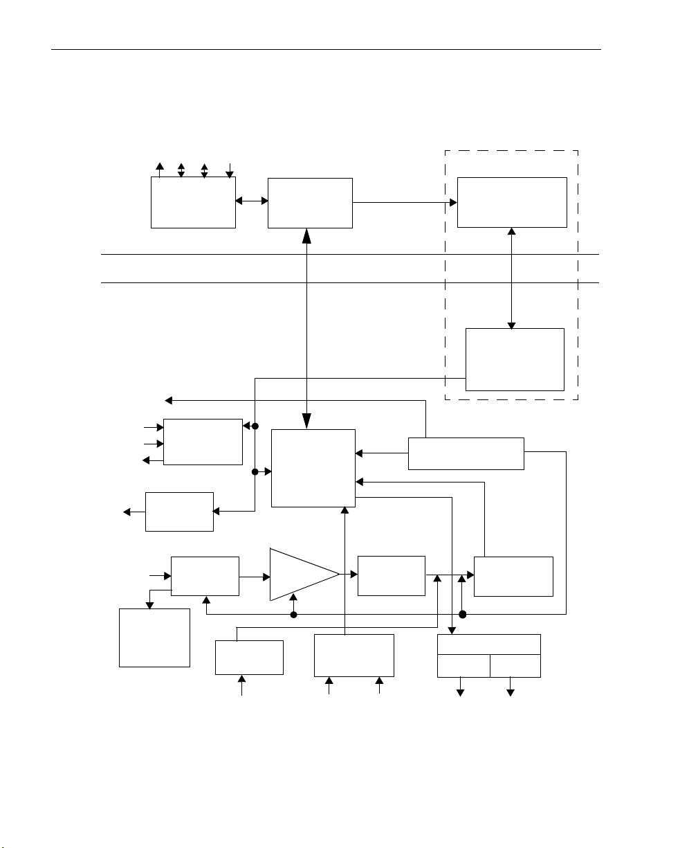
Figure 1 shows a block diagram of the KUSB-3102 and KUSB-3108
modules. Note that bold entries indicate signals you can access.
+5 V
D+
D−
Ground
USB
Interface
500 V Isolation Barrier *
Dynamic
Digital Out
Clock
Gate
Out
16 SE/8 DI
Analog
Inputs
Two 16-bit
User
Counter/Timers
8 Digital
Outputs
Analog Input
MUX
MicroController
High-Speed
Isolated Data Path
Isolated Side
Control Logic*
PGA
12- or 16-Bit
ADC
Isolated DC-DC
and Power Control*
Isolated
Powe r*
Channel Gain List
(32) Entries
Sample FIFO
10 kΩ Bias
Return
Termination
Resistors
8 Digital
Inputs
External
Clock and
Trigger Logic
Tri gger
Clock
12-or 16-Bit D/A
DAC0
DAC1
Figure 1: Block Diagram of the KUSB-3102 and KUSB-3108 Modules
6
Page 21

Analog Input Features
This section describes the features of the analog input (A/D)
subsystem, including the following:
• Input resolution, described on this page;
• Analog input channels, described on page 7;
• Input ranges and gains, described on page 12;
Principles of Operation
2
2
• A/D sample clock sources, described on page 14;
• Analog input conversion modes, described on page 16;
• Triggers, described on page 16;
• Data formats, described on page 23;
• Data transfer, described on page 25; and
• Error conditions, described on page 26.
Input Resolution
The input resolution of the KUSB-3102 is 12-bits, while the input
resolution of the KUSB-3108 module is 16-bits. Note that the
resolution is fixed; it cannot be programmed in software.
Analog Input Channels
Both the KUSB-3102 and KUSB-3108 modules support 16
single-ended or pseudo-differential analog input channels, or eight
differential analog input channels.
2
2
2
2
2
2
In addition, the KUSB-3108 module provides a cold junction
compensation (CJC) circuit on channel 0 at 10 mV/
you can connect seven thermocouple inputs (in differential mode) to
the KUSB-3108 module.
° C. Using the CJC,
2
7
Page 22

Chapter 2
You configure the channel type as single-ended or differential
through software. Using software, you can also select whether to use
10 kΩ termination resistance between the low side of each differential
channel and isolated analog ground. This feature is particularly
useful with floating signal sources. Refer to the KUSB-3102 and
KUSB-3108 Getting Started Manual for more information on wiring to
inputs and configuring the driver to use bias return termination
resistance.
Note: For pseudo-differential inputs, specify single-ended in
software; in this case, how you wire these signals determines the
configuration.
The KUSB-3102 and KUSB-3108 modules can acquire data from a
single analog input channel or from a group of analog input
channels. Channels are numbered 0 to 15 for single-ended and
pseudo-differential inputs, and 0 to 7 for differential inputs. The
following subsections describe how to specify the channels.
Specifying a Single Channel
The simplest way to acquire data from a single channel is to specify
the channel for a single-value analog input operation using software;
refer to page 16 for more information on single-value operations.
You can also specify a single channel using the analog input channel
list, described in the next section.
Note: If you want to perform a single-value digital input operation
while the A/D subsystem is configured, specify channel 16 (which
corresponds to the digital input port) in the A/D single-value
operation.
8
Page 23

Specifying One or More Channels
Principles of Operation
You can read data from one or more analog input channels using an
analog input channel list. You can group the channels in the list
sequentially (starting either with 0 or with any other analog input
channel) or randomly. You can also specify a single channel or the
same channel more than once in the list.
Using software, specify the channels in the order you want to sample
them. You can enter up to 32 entries in the channel list. The channels
are read in order (using continuously paced scan mode or triggered
scan mode) from the first entry to the last entry in the channel list.
Refer to page 16 for more information on the supported conversion
modes.
Specifying Digital Input Lines in the Analog Input Channel List
In addition to the analog input channels, the KUSB-3102 and
KUSB-3108 modules allow you to read eight digital input lines (Port
A, lines 0 to 7) using the analog input channel list. This feature is
particularly useful when you want to correlate the timing of analog
and digital events.
2
2
2
2
2
2
To read these eight digital input lines, specify channel 16 in the
analog input channel list. You can enter channel 16 anywhere in the
list and can enter it more than once, if desired.
Note: If channel 16 is the only channel in the channel-gain list, the
module can read this channel at the maximum A/D sampling rate.
2
2
2
9
Page 24

Chapter 2
The digital channel is treated like any other channel in the analog
input channel list; therefore, all the clocking, triggering, and
conversion modes supported for analog input channels are
supported for these digital input lines, if you specify them this way.
Performing Dynamic Digital Output Operations
Using software, you can enable a synchronous dynamic digital
output operation for the A/D subsystem. This feature is particularly
useful for synchronizing and controlling external equipment.
One dynamic digital output line (0) is provided (screw terminal 46).
This line is set to a value of 0 on power up; a reset does not affect the
values of the dynamic digital output line. Note that this line is
provided in addition to the other eight digital output lines; see page
32 for more information on the digital I/O features.
You specify the value (0 or 1) to write from the dynamic digital
output line using a digital channel list. A value of 0 indicates a
low-level signal; a value of 1 indicates a high-level signal.
10
The digital channel list corresponds to the analog input channel list.
As each entry in the analog input channel list is read, the
corresponding value you specified in the digital channel list is output
to the dynamic digital output line.
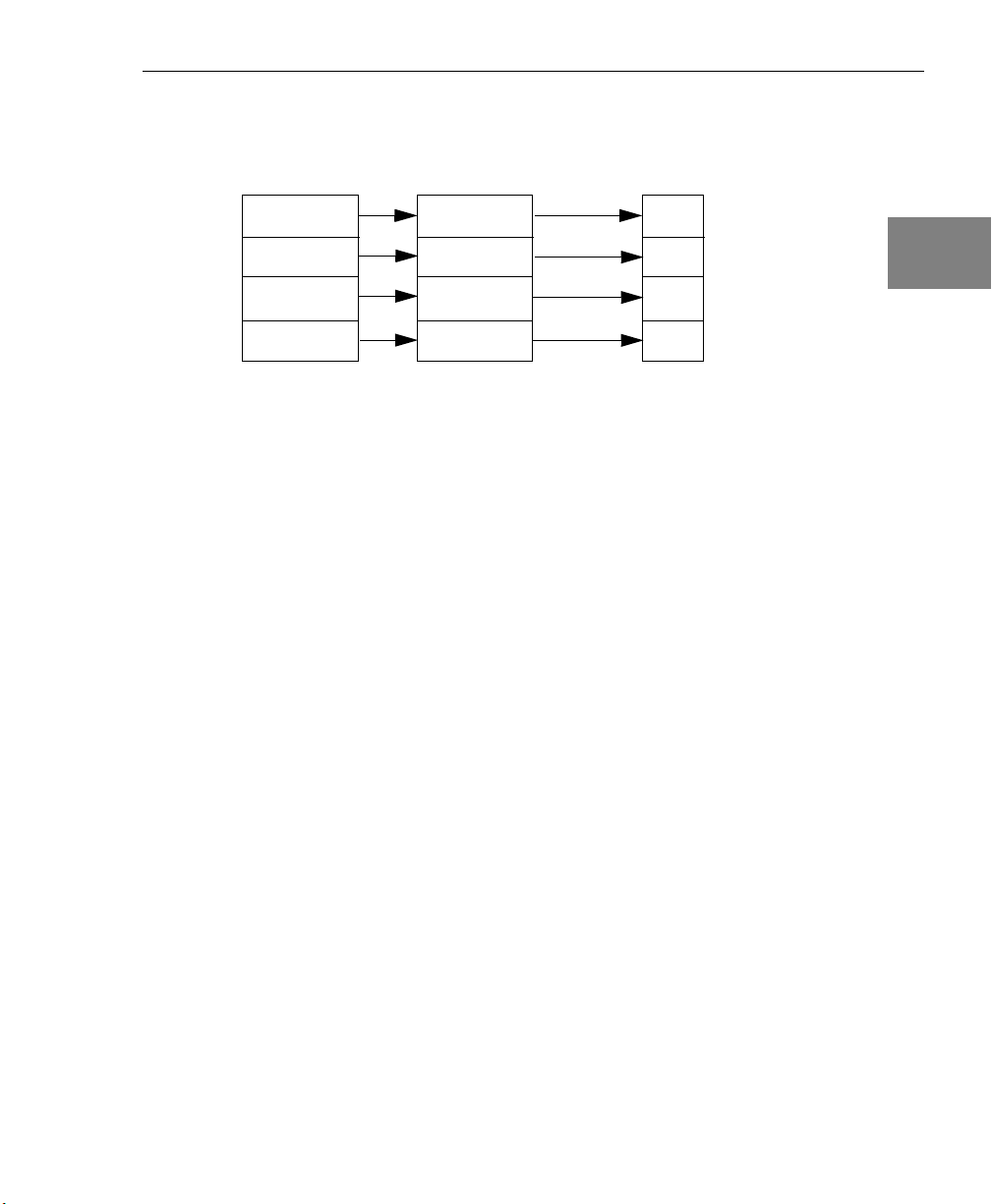
For example, assume that the analog input channel list contains
channels 0, 1, 2, and 3; that dynamic digital output operations are
enabled; and that the values in the digital channel list are 1, 0, 0, 1.
Figure 2 shows this configuration.
Page 25
Principles of Operation
Analog
Channel List
0
1
2
3
Figure 2: An Example Using Dynamic Digital Outputs
As analog input channel 0 is read, a high-level signal is output to the
dynamic digital output line. As analog input channels 1 and 2 are
read, a low-level signal is output to the dynamic digital output line.
As analog input channel 3 is read, a high-level signal is output to the
dynamic digital output line.
On power up, a value of 0 is written to the dynamic digital output
line.
Digital
Channel List
1
0
0
1
Dynamic Digital
Output Line 0
1
0
0
1
2
2
2
2
2
2
2
2
2
11
Page 26

Chapter 2
Input Ranges and Gains
Table 2 lists the supported gains and effective input ranges of the
KUSB-3102 and KUSB-3108 modules.
Table 2: Effective Input Ranges
Unipolar Input
Module Gain
KUSB-3102 1 0 to 10 V ±10 V
2 0 to 5 V ±5 V
4 0 to 2.5 V ±2.5 V
8 0 to 1.25 V ±1.25 V
KUSB-3108 1 − ±10 V
10 − ±1 V
100 − ±0.10 V
500 − ±0.020 V
Range
Bipolar Input
Range
Using software, specify 0 to 10 V for unipolar ranges or −10 V to +10 V
for bipolar ranges. Note that you specify the range for the entire
analog input subsystem, not the range per channel.
For each channel, choose the gain that has the smallest effective range
that includes the signal you want to measure. For example, if you are
using a KUSB-3102 and the range of your analog input signal is
±1.05 V, specify a range of −10 V to +10 V for the module and use a
gain of 8 for the channel; the effective input range for this channel is
then ±1.25 V, which provides the best sampling accuracy for that
channel.
12
The way you specify gain depends on how you specified the
channels, as described in the following subsections.
Page 27

Principles of Operation
Note: For single-value operations, the KUSB-3108 module supports
autoranging, where the module determines the appropriate gain for
your range rather than you having to specify it. Refer to page 16 for
more information on using autoranging.
Specifying the Gain for a Single Channel
The simplest way to specify gain for a single channel is to specify the
gain for a single-value analog input operation using software; refer to
page 16 for more information on single-value operations.
You can also specify the gain for a single channel using an analog
input gain list, described in the next section.
Specifying the Gain for One or More Channels
For the KUSB-3102 and KUSB-3108 modules, you can specify the gain
for one or more analog input channels using an analog input gain list.
Using software, set up the gain list by specifying the gain for each
entry in the channel list. (The two lists together are often referred to
as the channel-gain list.)
2
2
2
2
2
2
For example, assume the analog input channel list contains three
entries: channels 5, 6, and 7; the gain list might look like this: 2, 4, 1,
where a gain of 2 corresponds to channel 5, a gain of 4 corresponds to
channel 6, and a gain of 1 corresponds to channel 7.
Note: For analog input channel 16 (the eight digital input lines) in
the channel list, specify a gain of 1 in the gain list.
2
2
2
13
Page 28

Chapter 2
A/D Sample Clock Sources
The KUSB-3102 and KUSB-3108 modules allow you to use one of two
clock sources for pacing analog input operations in continuous mode:
• The internal A/D sample clock, which uses the 24-bit A/D
Counter on the module, or
• An external A/D sample clock, which you can connect directly to
the screw terminals on the module.
You use an A/D sample clock to pace the acquisition of each channel
in the channel-gain list; this clock is also called the A/D pacer clock.
Note: If you enter digital input channel 16 in the channel-gain list,
the A/D sample clock (internal or external) also paces the
acquisition of the eight digital input lines.
The following subsections describe the internal and external A/D
sample clocks in more detail.
14
Internal A/D Sample Clock
The internal A/D sample clock uses a 12 MHz time base.
Conversions start on the rising edge of the counter output; the output
pulse is active low.
Using software, specify the clock source as internal and the clock
frequency at which to pace the operation. The minimum frequency
supported is 0.75 Hz (0.75 Samples/s).
The maximum frequency of the KUSB-3102 module is
100 kSamples/s.
Page 29

Principles of Operation
For the KUSB-3108 module, the maximum frequency is
50 kSamples/s for a single channel or a channel scan when the gain is
1 or 10. When the gain is 100, the maximum frequency is
10 kSamples/s. When the gain is 500, the maximum frequency is 2
kSamples/s.
2
According to sampling theory (Nyquist Theorem), specify a
frequency that is at least twice as fast as the input’s highest frequency
component. For example, to accurately sample a 20 kHz signal,
specify a sampling frequency of at least 40 kHz. Doing so avoids an
error condition called aliasing, in which high frequency input
components erroneously appear as lower frequencies after sampling.
External A/D Sample Clock
An external A/D sample clock is useful when you want to pace
acquisitions at rates not available with the internal A/D sample clock
or when you want to pace at uneven intervals.
Connect an external A/D sample clock to screw terminal TB25 on the
module (pin 25 on connector J1). Conversions start on the rising edge
of the external A/D sample clock input signal.
Using software, specify the clock source as external. The clock
frequency is always equal to the frequency of the external A/D
sample clock input signal that you connect to the module.
2
2
2
2
2
2
2
2
15
Page 30

Chapter 2
Triggers
A trigger is an event that occurs based on a specified set of
conditions. KUSB-3102 and KUSB-3108 modules support the
following trigger sources:
• Software trigger − A software trigger event occurs when you start
the analog input operation (the computer issues a write to the
module to begin conversions). Using software, specify the trigger
source as a software trigger.
• External trigger − An external digital trigger event occurs when
the module detects a rising edge on the Ext A/D Trigger input
signal connected to screw terminal TB24 on the module (pin 24 of
connector J1). The trigger signal is TTL-compatible. Using
software, specify the trigger source as a external digital trigger
(external for DataAcq SDK users).
Analog Input Conversion Modes
The KUSB-3102 and KUSB-3108 modules support the following
conversion modes:
16
• Single-value operations are the simplest to use. Using software,
you can either specify the range, gain, and analog input channel,
or you can specify the range and analog input channel and have
the software determine the best gain for the range (called
autoranging). The board acquires the data from the specified
channel and returns the data immediately. Data can be returned
as both counts and voltage. For a single-value operation, you
cannot specify a clock source, trigger source, scan mode, or
buffer.
Single-value operations stop automatically when finished; you
cannot stop a single-value operation.
Page 31

Principles of Operation
• Scan mode takes full advantage of the capabilities of the
KUSB-3102 and KUSB-3108 modules. In a scan, you can specify a
channel-gain list, clock source, trigger source, scan mode, buffer,
and buffer wrap mode using software. Two scan modes are
supported: continuously paced scan mode and triggered scan
mode (often called burst mode). These modes are described in
the following subsections.
Using software, you can stop a scan by performing either an
orderly stop or an abrupt stop. In an orderly stop, the module
finishes acquiring the data, stops all subsequent acquisition, and
transfers the acquired data to host memory; all subsequent
triggers or retriggers are ignored.
In an abrupt stop, the module stops acquiring samples
immediately; the acquired data is not transferred to host memory,
and all subsequent triggers or retriggers are ignored.
2
2
2
2
Continuously Paced Scan Mode
Use continuously paced scan mode if you want to accurately control
the period between conversions of individual channels in a scan.
When it detects an initial trigger, the module cycles through the
channel-gain list, acquiring and converting the value for each entry in
the list (this process is defined as the scan). The module then wraps to
the start of the channel-gain list and repeats the process continuously
until either the allocated buffers are filled or until you stop the
operation. Refer to page 25 for more information on buffers.
The conversion rate is determined by the frequency of the A/D
sample clock; refer to page 14 for more information on the A/D
sample clock. The sample rate, which is the rate at which a single
entry in the channel-gain list is sampled, is determined by the
frequency of the A/D sample clock divided by the number of entries
in the channel-gain list.
2
2
2
2
2
17
Page 32

Chapter 2
To select continuously paced scan mode, use software to specify the
dataflow as continuous and to specify a trigger source to start the
operation. Refer to page 16 for more information on the supported
trigger sources.
Figure 3 illustrates continuously paced scan mode using a
channel-gain list with three entries: channel 0, channel 1, and channel
2. In this example, analog input data is acquired on each clock pulse
of the A/D sample clock. When it reaches the end of the channel-gain
list, the module wraps to the beginning of the channel-gain list and
repeats this process. Data is acquired continuously.
Chan 0
Chan 1
A/D
Sample
Clock
Trigger event occurs
Figure 3: Continuously Paced Scan Mode
Chan 2
Chan 0
Data acquired continuously
Chan 2
Chan 1
Chan 0
Chan 1
Chan 2
Chan 0
Chan 1
Chan 2
18
Page 33

Triggered Scan Mode
Principles of Operation
KUSB-3102 and KUSB-3108 modules support two triggered scan
modes: internally retriggered and externally retriggered. These
modes are described in the following subsections.
Internally Retriggered Scan Mode
Use internally retriggered scan mode if you want to accurately
control both the period between conversions of individual channels
in a scan and the period between each scan. This mode is useful when
synchronizing or controlling external equipment or when acquiring a
buffer of data on each trigger or retrigger.
When it detects an initial trigger (either a software trigger or an
external trigger), the module scans the channel-gain list once, then
waits for an internal retrigger to occur. When it detects an internal
retrigger, the board scans the channel-gain list once again, then waits
for another internal retrigger to occur. The process repeats
continuously until either the allocated buffers are filled or until you
stop the operation; refer to page 25 for more information on buffers.
The sample rate is determined by the frequency of the A/D sample
clock divided by the number of entries in the channel-gain list; refer
to page 14 for more information on the A/D sample clock. The
conversion rate of each scan is determined by the frequency of the
internal retrigger clock. The internal retrigger clock is the Triggered
Scan Counter on the board; the Triggered Scan Counter is a 24-bit
counter with a 12 MHz clock.
2
2
2
2
2
2
2
Figure 4 illustrates triggered scan mode. In this example, post-trigger
analog input data is acquired on each clock pulse of the A/D sample
clock until the channel-gain list has been scanned once; then, the
board waits for the retrigger event. When the retrigger event occurs,
the board scans the channel-gain list once again, acquiring data on
each pulse of the A/D sample clock. The process repeats
continuously with every specified retrigger event.
2
2
19
Page 34

Chapter 2
Chan 0
Chan 1
A/D
Sample
Clock
Trigger event occurs;
data acquired for one
scan of the CGL.
Specify the frequency of the internal retrigger clock using software.
The minimum retrigger frequency is 0.75 Hz (0.75 Samples/s).
The maximum retrigger rate of the KUSB-3102 module is 100 kHz.
For the KUSB-3108 module, the maximum retrigger frequency is
50 kHz for a single channel or a channel scan when the gain is 1 or 10.
When the gain is 100, the maximum retrigger frequency is 10 kHz.
When the gain is 500, the maximum retrigger frequency is 2 kHz.
Chan 2
Board waits for
retrigger event.
Chan 0
Retrigger event occurs;
data acquired for one
scan of the CGL.
Figure 4: Triggered Scan Mode
Chan 2
Chan 1
20
The appropriate retrigger frequency depends on a number of factors,
determined by the following equations:
Min. Retrigger = # of CGL entries + 2 µs
Period A/D sample clock frequency
Max. Retrigger = 1
Frequency Min. Retrigger Period
Page 35

Principles of Operation
For example, if you are using 16 channels in the channel-gain list, and
using an A/D sample clock with a frequency of 50 kHz, set the
maximum retrigger frequency to 3.106 kHz, since
3.106 kHz = 1
16 + 2 µs
50 kHz
To select internally retriggered scan mode, use software to specify the
following parameters:
• The dataflow as continuous;
• Triggered scan mode usage as enabled;
2
2
2
• The retrigger mode as internal;
• The number of times to scan per trigger or retrigger (also called
the multiscan count) as 1;
• The frequency of the retrigger clock; and
• The initial trigger source; refer to page 16 for more information
on the supported trigger sources.
Externally Retriggered Scan Mode
Use externally retriggered scan mode if you want to accurately
control the period between conversions of individual channels and
retrigger the scan based on an external event.
When a module detects an initial trigger (either a software trigger or
an external trigger), the module scans the channel-gain list once, then
waits for an external retrigger to occur. The external retrigger occurs
when a rising edge is detected on the Ext A/D Trigger input screw
terminal (TB24) on the module.
2
2
2
2
2
2
21
Page 36

Chapter 2
When the retrigger occurs, the module scans the channel-gain list
once, then waits for another external retrigger to occur. The process
repeats continuously until either the allocated buffers are filled (if
buffer wrap mode is none) or until you stop the operation (if buffer
wrap mode is single or multiple); refer to page 25 for more
information on buffers.
The conversion rate of each channel is determined by the frequency
of the A/D sample clock; refer to page 14 for more information on the
A/D sample clock. The conversion rate of each scan is determined by
the period between external retriggers; therefore, it cannot be
accurately controlled. The module ignores external triggers that occur
while it is acquiring data. Only external retrigger events that occur
when the module is waiting for a retrigger are detected and acted on.
To select externally retriggered scan mode, use software to specify the
following parameters:
• The dataflow as continuous;
• The triggered scan mode usage as enabled;
• The retrigger mode as an external retrigger (retrigger extra for
DataAcq SDK users);
22
• The number of times to scan per trigger or retrigger (also called
the multiscan count) to 1; and
• The retrigger source as the external trigger (external for DataAcq
SDK users).
Note: For DataAcq SDK users, if you want to use the same trigger
source as both the initial trigger and the retrigger source, specify the
external trigger as the initial trigger source and specify the retrigger
mode as scan-per-trigger. In this case, you need not specify the
retrigger source; the module uses the initial trigger source as the
retrigger source.
Page 37

Data Format
Principles of Operation
The KUSB-3102 module uses straight binary data encoding. The
KUSB-3108 module uses offset binary data encoding.
In software, the analog input value is returned as a code. To convert
the code to voltage, use the following formulas:
LSB = FSR
Vin = Code * LSB + Offset
where,
• LSB is the least significant bit.
• FSR is the full-scale range. The full-scale range is 10 for the
• N is the input resolution (12-bits for the KUSB-3102 and 16-bits
• Vin is the analog voltage.
• Code is the raw count used by the software to represent the
N
2
unipolar range or 20 for the bipolar range.
for the KUSB-3108).
voltage.
2
2
2
2
2
2
• Offset is the actual minus full-scale value. The minus full-scale
value is 0.0 V for the unipolar input range and −10 V for the
bipolar input range.
2
2
2
23
Page 38

Chapter 2
For example, assume that you are using a KUSB-3102 with a unipolar
input range. If the software returns a code of 2010 for the analog
input operation, determine the analog input voltage as follows:
LSB = 10 = 0.002441 V + 0.0 V
4096
Vin = 2010 * 0.002441 + 0 V
Vin = 4.906 V
Similarly, assume that you are using a KUSB-3108 module with a
bipolar input range. The actual minus full-scale value is −10.0 V. If
the software returns a code of 2010 for the analog input operation,
determine the analog input voltage as follows:
LSB = 20 = 0.000305 V
65536
Vin = 2010 * 0.000305 + −10.0 V
24
Vin = −9.370 V
Table 3 lists the values that are returned when the KUSB-3102 or
KUSB-3108 module is overrange.
Table 3: Overrange SIgnal Values
Module
Name
KUSB-3102 FFFh
KUSB-3108 FFFFh
Above-Range
Signals
(plus full-scale)
(plus full-scale)
Below-Range
000h
(minus full-scale)
0000h
(minus full-scale)
Signals
Page 39

Data Transfer
Principles of Operation
The module packs two bytes into each transfer to the host computer.
Even samples (corresponding to entries 0, 2, 4, and so on, in the
channel-gain list) are packed into the low bytes; odd samples
(corresponding to entries 1, 3, 5, and so on, in the channel-gain list)
are packed into the high bytes.
Both the KUSB-3102 and KUSB-3108 modules contain a 2048-sample
FIFO. During a continuous analog input operation, the hardware
interrupts the firmware on the module when the FIFO is half full. The
module then transfers 2048 samples to a circular buffer, which is
dedicated to the hardware, in the host computer.
The device driver accesses the hardware circular buffer to fill user
buffers that you allocate in software. Keep the following
recommendations in mind when allocating user buffers for
continuous analog input operations on the module:
• Allocate a minimum of three user buffers.
• Specify a buffer size at least as large as the sampling rate; for
example, if you are using a sampling rate of 100 kSamples/s
(100 kHz), specify a buffer size of 100,000. The minimum buffer
size that you should specify is 256 samples.
2
2
2
2
2
2
Note: If you are using a slow clock data rate, such as .75 Hz, and
a 256 sample user buffer, you will have to wait over 5 minutes for
any data since data is transferred only when 256 samples have
been read.
2
2
2
25
Page 40

Chapter 2
• Specify one of the following buffer wrap modes:
− If the wrap mode is none, data is written to the allocated
buffers until no more empty buffers are available; at that
point, the operation stops.
− If wrap mode is multiple, data is written to the allocated
multiple buffers continuously; when no more empty buffers
are available, the module overwrites the data in the filled
buffers starting with the first location of the first buffer. This
process continues indefinitely until you stop it.
− If wrap mode is single, data is written to a single buffer
continuously; when the buffer is filled, the module overwrites
the data in the buffer starting with the first location of the
buffer. This process continues indefinitely until you stop it.
Error Conditions
The KUSB-3102 and KUSB-3108 modules report an error if one of the
following conditions occurs:
26
• A/D Over Sample error − The A/D sample clock rate is too fast.
This error is reported if a new A/D sample clock pulse occurs
while the ADC is busy performing a conversion from the
previous A/D sample clock pulse. The host computer can clear
this error.
To avoid this error, use a slower sampling rate.
• A/D FIFO Full Flag set to 1 − The data was not read fast enough
by the host computer. The host computer can clear this error.
To avoid this error, ensure that you allocated at least three
buffers, each at least as large as the sampling rate; for example, if
you are using a sampling rate of 100 kSamples/s (100 kHz),
specify a buffer size of 100,000 samples for each buffer.
If one of these error conditions occurs, the module reports the
error but continues to acquire and transfer data to the host
computer.
Page 41

Principles of Operation
Note: The LED on the front panel will not blink green if the
hardware detects an error.
2
2
2
2
2
2
2
2
2
27
Page 42

Chapter 2
Analog Output Features
Both the KUSB-3102 and KUSB-3108 modules contain an analog
output (D/A) subsystem. This section describes the following
features of the D/A subsystem:
• Output resolution, described on this page;
• Analog output channels, described on page 28;
• Output ranges and gains, described on page 29;
• Conversion modes, described on page 30; and
• Data format, described on page 30.
Output Resolution
The KUSB-3102 module provides an output resolution of 12-bits. The
KUSB-3108 module provides an output resolution of 16-bits. Note
that the resolution is fixed; it cannot be programmed in software.
28
Analog Output Channels
Both the KUSB-3102 and KUSB-3108 modules support two DC-level
analog output channels (DAC0 and DAC1). Refer to the KUSB-3102
and KUSB-3108 Getting Started Manual for information on how to wire
analog output signals to the module. You configure the channel type
through software.
Within each DAC, the digital data is double-buffered to prevent
spurious outputs, then output as an analog signal. Both DACs power
up to a value of 0 V ±10 mV. Resetting the module does not clear the
values in the DACs.
Page 43

Principles of Operation
The module can output data from a single analog output channel
only. Specify the channel for a single-value analog output operation
using software; refer to “Conversion Modes,” on page 30 for more
information on single-value operations.
2
Output Ranges and Gains
Table 4 lists the output ranges supported by the KUSB-3102 and
KUSB-3108 modules. The gain is always 1.
Table 4: Output Ranges
Unipolar Output
Module
KUSB-3102 0 to 10 V or
KUSB-3108
Specify the range using software.
Range
0 to 5 V
−
Bipolar Input
Range
±10 V or ±5 V
±10 V
2
2
2
2
2
2
2
2
29
Page 44

Chapter 2
Conversion Modes
KUSB-3102 and KUSB-3108 modules can perform single-value analog
output operations only. Use software to specify the range, gain, and
analog output channel, then output the data from the specified
channel. You cannot specify a clock source, trigger source, or buffer.
Note: You cannot perform a single-value analog output operation
while the A/D subsystem is running.
The settling time for each DAC is 50 µs (20 V steps).
Single-value operations stop automatically when finished; you
cannot stop a single-value operation.
Data Format
30
Data from the host computer must use offset binary data encoding for
analog output signals. Using software, specify the data encoding as
binary.
In software, you need to supply a code that corresponds to the analog
output value you want the module to output. To convert a voltage to
a code, use the following formulas:
LSB = FSR
Code = Vout - offset
N
2
LSB
Page 45

where,
Principles of Operation
• LSB is the least significant bit.
• FSR is the full-scale range (10).
• N is the output resolution (12-bits for the KUSB-3102 module and
16-bits for the KUSB-3108 module).
• Code is the raw count used by the software to represent the
voltage.
• Vout is the analog voltage.
• Offset is the minus full-scale value, or −10 V.
For example, assume that you are using a KUSB-3108 module. If you
want to output a voltage of 4.7 V, determine the code value as
follows:
LSB = 10 V = 0.0001526 V
65536
Code = 4.7 V - (-10 V)
0.0001526 V
Code = 96330 = 1784Ah
2
2
2
2
2
2
2
2
2
31
Page 46

Chapter 2
Digital I/O Features
This section describes the following features of the digital I/O
subsystem:
• Digital I/O lines, described on this page;
• Resolution, described on this page; and
• Operation modes, described on page 33.
Digital I/O Lines
KUSB-3102 and KUSB-3108 modules support eight digital input lines
(Port A, lines 0 to 7) through the DIN subsystem and eight digital
output lines (Port B, lines 0 to 7) through the DOUT subsystem.
For fast, clocked digital input operations, you can enter the digital
input lines from Port A as channel 16 in the analog input channel list;
refer to page 9 for more information.
Both modules also provide a dynamic digital output line that you can
update when an analog input channel is read. Note that the dynamic
digital output line is in addition to the digital output lines in Port B.
Refer to page 10 for more information on dynamic digital output
operations.
32
On power up or module reset, no digital data is output from the
modules. All the outputs include diode protection to the isolated
ground and the isolated +5 V.
Resolution
The resolution of the digital input port is fixed at 8 bits; the resolution
of the digital output port is also fixed at 8 bits.
You cannot program the digital I/O resolution in software.
Page 47

Operation Modes
Principles of Operation
KUSB-3102 and KUSB-3108 modules support the following digital
I/O operation modes:
• Single-value operations are the simplest to use but offer the least
flexibility and efficiency. You use software to specify the digital
I/O port and a gain of 1 (the gain is ignored). Data is then read
from or written to the digital I/O lines. For a single-value
operation, you cannot specify a clock or trigger source.
Single-value operations stop automatically when finished; you
cannot stop a single-value operation.
• Continuous digital input takes full advantage of the capabilities
of the modules. In this mode, enter all eight digital input lines of
Port A as channel 16 of the analog input channel-gain list;
program this mode through the A/D subsystem. Using this
mode, you can specify a clock source, scan mode, trigger source,
buffer, and buffer wrap mode for the digital input operation.
Refer to page 9 for more information on specifying digital input
lines for a continuous digital input operation.
• Dynamic digital output is useful for synchronizing and
controlling external equipment and allows you to output data to
the dynamic digital output line each time an analog input value
is acquired. This mode is programmed through the A/D
subsystem; refer to page 10 for more information.
2
2
2
2
2
2
2
2
2
33
Page 48

Chapter 2
Counter/Timer Features
The counter/timer circuitry on the module provides the clocking
circuitry used by the A/D and D/A subsystems as well as several
user counter/timer features. This section describes the following user
counter/timer features:
• Units, described on this page;
• C/T clock sources, described on page 35;
• Gate types, described on page 37;
• Pulse types and duty cycles, described on page 39; and
• Counter/timer operation modes, described on page 40.
Units
Two 16-bit counter/timers (0 and 1) are supported by the KUSB-3102
and KUSB-3108 modules.
Each counter accepts a clock input signal and gate input signal and
outputs a clock output signal (also called a pulse output signal), as
shown in Figure 5.
34
Clock Input SIgnal
(internal, external,
or internally
cascaded)
Counter
Gate Input Signal
(software or
external input)
Figure 5: Counter/Timer Channel
Pulse Output
Signal
Page 49

Principles of Operation
Each counter corresponds to a counter/timer (C/T) subsystem. To
specify the counter to use in software, specify the appropriate C/T
subsystem. Counter 0 corresponds to C/T subsystem element 0;
counter 1 corresponds to C/T subsystem element 1.
2
C/T Clock Sources
The following clock sources are available for the user counters:
• Internal C/T clock,
• External C/T clock, and
• Internally cascaded clock.
Refer to the following subsections for more information on these
clock sources.
Internal C/T Clock
The internal C/T clock uses a 12 MHz time base. Counter/timer
operations start on the rising edge of the clock input signal.
Through software, specify the clock source as internal and the
frequency at which to pace the counter/timer operation (this is the
frequency of the clock output signal). The maximum frequency that
you can specify for the clock output signal is 750 kHz. The minimum
frequency that you can specify for the clock output signal for each
16-bit counter is 183.1 Hz. The rising edge of the clock is the active
edge.
2
2
2
2
2
2
2
2
35
Page 50

Chapter 2
External C/T Clock
An external C/T clock is useful when you want to pace
counter/timer operations at rates not available with the internal C/T
clock or if you want to pace at uneven intervals. The rising edge of
the external C/T clock input signal is the active edge.
Using software, specify the clock source as external and the clock
divider used to determine the frequency at which to pace the
operation. The minimum clock divider that you can specify is 2.0; the
maximum clock divider that you can specify is 65,536. For example, if
you supply an external C/T clock with a frequency of 700 kHz and
specify a clock divider of 2, the resulting frequency of the external
C/T clock output signal is 350 kHz. The resulting frequency of the
external C/T clock output signal must not exceed 750 kHz.
Table 5 lists the screw terminals of the modules that correspond to
the external C/T clock signals of each counter/timer.
Table 5: External C/T Clock Signals
36
Counter/
Timer
0 TB54 54
1 TB50 50
Screw Terminal
on Module
Number
J1 Pin
Page 51

Internally Cascaded Clock
Principles of Operation
You can also internally route the clock output signal from
counter/timer 0 to the clock input signal of counter/timer 1 to
internally cascade the counters. In this way, you can create a 32-bit
counter without externally connecting two counters together.
Specify internal cascade mode in software. The rising edge of the
clock input signal is active.
Through software, specify the clock source as internal and the
frequency at which to pace the counter/timer operation (this is the
frequency of the clock output signal). The maximum frequency that
you can specify for the clock output signal is 750 kHz. For a 32-bit
cascaded counter, the minimum frequency that you can specify for
the clock output signal is 0.0028 Hz.
Gate Types
The active edge or level of the gate input to the counter enables
counter/timer operations. The operation starts when the clock input
signal is received. Specify the gate type in software.
KUSB-3102 and KUSB-3108 modules provide the following gate
input types:
2
2
2
2
2
2
• None − A software command enables any specified
counter/timer operation immediately after execution. This gate
type is useful for all counter/timer modes; refer to page 40 for
more information on these modes.
• Logic-low level external gate input − Enables a counter/timer
operation when the external gate signal is low, and disables the
counter/timer operation when the external gate signal is high.
Note that this gate type is used only for event counting,
frequency measurement, and rate generation; refer to page 40 for
more information on these modes.
2
2
2
37
Page 52

Chapter 2
• Logic-high level external gate input − Enables a counter/timer
operation when the external gate signal is high, and disables a
counter/timer operation when the external gate signal is low.
Note that this gate type is used only for event counting,
frequency measurement, and rate generation; refer to page 40 for
more information on these modes.
• Falling-edge external gate input − Enables a counter/timer
operation on the transition from the high level to the low level
(falling edge). In software, this is called a low-edge gate type.
Note that this gate type is used only for one-shot and repetitive
one-shot mode; refer to page 40 for more information on these
modes.
• Rising-edge external gate input − Enables a counter/timer
operation on the transition from the low level to the high level
(rising edge). In software, this is called a high-edge gate type.
Note that this gate type is used only for one-shot and repetitive
one-shot mode; refer to page 49 for more information on these
modes.
Table 6 lists the screw terminals and pin numbers on the modules
that correspond to the gate input signals of each counter/timer.
38
Table 6: Gate Input Signals
Counter/
Timer
0 TB52 52
1 TB48 48
Screw Terminal
on Module
Number
J1 Pin
Page 53

Pulse Output Types and Duty Cycles
Principles of Operation
KUSB-3102 and KUSB-3108 modules can output pulses from each
counter/timer. Table 7 lists the screw terminals of the modules that
correspond to the pulse output signals of each counter/timer.
Table 7: Pulse Output Signals
Counter/
Timer
0 TB53 53
1 TB49 49
Both modules support the following pulse output types on the clock
output signal:
• High-to-low transitions − The low portion of the total pulse
output period is the active portion of the counter/timer clock
output signal.
• Low-to-high transitions − The high portion of the total pulse
output period is the active portion of the counter/timer pulse
output signal.
Screw Terminal
on Module
J1 Pin
Number
2
2
2
2
2
2
You specify the pulse output type in software.
The duty cycle (or pulse width) indicates the percentage of the total
pulse output period that is active. A duty cycle of 50, then, indicates
that half of the total pulse is low and half of the total pulse output is
high. You specify the duty cycle in software.
Note: The minimum pulse width must be 650 ns.
2
2
2
39
Page 54

Chapter 2
Figure 6 illustrates a low-to-high pulse with a duty cycle of
approximately 30%.
Active Pulse Width
high pulse
low pulse
Total Pulse Period
Figure 6: Example of a Low-to-High Pulse Output Type
Counter/Timer Operation Modes
KUSB-3102 and KUSB-3108 modules support the following
counter/timer operation modes:
40
• Event counting,
• Frequency measurement,
• Rate generation,
• One-shot, and
• Repetitive one-shot.
The following subsections describe these modes in more detail.
Page 55

Event Counting
Principles of Operation
Use event counting mode to count events (clock pulses) from the
counter’s associated clock input source.
If you are using one counter, you can count a maximum of 65,536
events before the counter rolls over to 0 and starts counting again. If
you are using a cascaded 32-bit counter, you can count a maximum of
4,294,967,296 events before the counter rolls over to 0 and starts
counting again.
In event counting mode, use an external C/T clock source; refer to
page 36 for more information on the external C/T clock source.
Using software, specify the counter/timer mode as event counting
(count), the C/T clock source as external, and the gate type that
enables the operation as logic high. Refer to page 39 for information
on gates.
Ensure that the signals are wired appropriately. Refer to the
KUSB-3102 and KUSB-3108 Getting Started Manual for wiring
examples.
Figure 7 shows an example of an event counting operation using a
logic-high gate type.
2
2
2
2
2
2
2
2
2
41
Page 56

Chapter 2
Gate Input
Signal
External C/T
Clock
Input Signal
high level
enables operation
low level
disables operation
3 events are counted while
the operation is enabled
event counting
operation starts
event counting
operation stops
Figure 7: Example of Event Counting
Frequency Measurement
Use frequency measurement mode to measure the frequency of the
signal from counter’s associated clock input source over a specified
duration. In this mode, use an external C/T clock source; refer to
page 35 for more information on the external C/T clock source.
One way to perform a frequency measurement is to use the same
wiring as an event counting application that does not use an external
gate signal. Refer to the KUSB-3102 and KUSB-3108 Getting Started
Manual for wiring examples.
42
Page 57

Principles of Operation
In this configuration, use software to specify the counter/timer mode
as frequency measurement or event counting (count), and the
duration of the system timer over which to measure the frequency.
(The system timer uses a resolution of 1 ms.) In this configuration,
frequency is determined using the following equation:
2
Frequency Measurement = Number of Events
Duration of the System Timer
If you need more accuracy than the system timer provides, you can
connect a pulse of a known duration (such as a one-shot output of
another user counter) to the external gate input. Refer to the
KUSB-3102 and KUSB-3108 Getting Started Manual for wiring
examples.
In this configuration, use software to set up the counter/timers as
follows:
1. Set up one of the counter/timers for one-shot mode, specifying
the clock source, clock frequency, gate type, type of output pulse
(high or low), and duty cycle.
2. Set up the counter/timer that will measure the frequency for
event counting mode, specifying the clock source to count, and
the gate type (this should match the pulse output type of the
counter/timer set up for one-shot mode).
3. Start both counters (events are not counted until the active period
of the one-shot pulse is generated).
4. Read the number of events counted. (Allow enough time to
ensure that the active period of the one-shot occurred and that
events have been counted.)
5. Determine the measurement period using the following
equation:
2
2
2
2
2
2
2
Measurement period = 1 * Active Pulse Width
Clock Frequency
2
43
Page 58

Chapter 2
External C/T
Clock
Input Signal
6. Determine the frequency of the clock input signal using the
following equation:
Frequency Measurement = Number of Events
Measurement Period
Figure 8 shows an example of a frequency measurement operation. In
this example, three events are counted during a duration of 300 ms.
The frequency, then, is 10 Hz, since 10 Hz = 3/(.3 s).
3 Events Counted
Duration over which the
frequency is measured = 300 ms
frequency measurement
starts
frequency
measurement stops
44
Figure 8: Example of Frequency Measurement
Rate Generation
Use rate generation mode to generate a continuous pulse output
signal from the counter; this mode is sometimes referred to as
continuous pulse output or pulse train output. You can use this pulse
output signal as an external clock to pace other operations, such as
analog input or other counter/timer operations.
While the pulse output operation is enabled, the counter outputs a
pulse of the specified type and frequency continuously. As soon as
the operation is disabled, rate generation stops.
Page 59

Principles of Operation
The period of the output pulse is determined by the clock input
signal and the external clock divider. If you are using one counter
(not cascaded), you can output pulses using a maximum frequency of
1 MHz (this is the frequency of the clock output signal). In rate
generation mode, either the internal or external C/T clock input
source is appropriate depending on your application; refer to page 35
for more information on the C/T clock source.
Using software, specify the counter/timer mode as rate generation
(rate), the C/T clock source as either internal or external, the polarity
of the output pulses (high-to-low transitions or low-to-high
transitions), the duty cycle of the output pulses, and the gate type
that enables the operation as logic-high. Refer to page 39 for more
information on pulse output signals and to page 37 for more
information on gate types.
Ensure that the signals are wired appropriately. Refer to the
KUSB-3102 and KUSB-3108 Getting Started Manual for wiring
examples.
Figure 9 shows an example of an enabled rate generation operation
using a logic-high gate input signal, an external C/T clock source
with an input frequency of 4 kHz, a clock divider of 4, a low-to-high
pulse type, and a duty cycle of 75%. A 1 kHz square wave is the
generated output. Figure 10 shows the same example using a duty
cycle of 25%.
2
2
2
2
2
2
2
2
2
45
Page 60

Chapter 2
Rate Generation
Operation Starts
External C/T
Clock
Input Signal
(4 kHz)
Pulse
Output
Signal
75% duty cycle
Figure 9: Example of Rate Generation Mode with a 75% Duty Cycle
Continuous Pulse
Output Operation Starts
External C/T
Clock
Input Signal
(4 kHz)
Pulse
Output
Signal
25% duty cycle
46
Figure 10: Example of Rate Generation Mode with a 25% Duty Cycle
Page 61

One-Shot
Principles of Operation
Use one-shot mode to generate a single pulse output signal from the
counter when the operation is triggered (determined by the gate
input signal). You can use this pulse output signal as an external
digital (TTL) trigger to start other operations, such as analog input
operations.
When the one-shot operation is triggered, a single pulse is output;
then, the one-shot operation stops. All subsequent clock input signals
and gate input signals are ignored.
The period of the output pulse is determined by the clock input
signal. In one-shot mode, the internal C/T clock source is more useful
than an external C/T clock source; refer to page 35 for more
information on the internal C/T clock source.
Using software, specify the counter/timer mode as one-shot, the
clock source as internal, the polarity of the output pulse (high-to-low
transition or low-to-high transition), the duty cycle of the output
pulse, and the gate type to trigger the operation as rising edge or
falling edge. Refer to page 39 for more information on pulse output
types and to page 37 for more information on gate types.
2
2
2
2
2
2
Note: In the case of a one-shot operation, use a duty cycle as close
to 100% as possible to output a pulse immediately. Using a duty
cycle closer to 0% acts as a pulse output delay.
Ensure that the signals are wired appropriately. Refer to the
KUSB-3102 and KUSB-3108 Getting Started Manual for wiring
examples.
2
2
2
47
Page 62

Chapter 2
Figure 11 shows an example of a one-shot operation using an external
gate input (rising edge), a clock output frequency of 1 kHz (pulse
period of 1 ms), a low-to-high pulse type, and a duty cycle of 99.99%.
Figure 12 shows the same example using a duty cycle of 50%.
One-Shot Operation
Starts
External
Gate
Signal
1 ms period
99.99% duty cycle
Pulse
Output
Signal
48
Figure 11: Example of One-Shot Mode Using a 99.99% Duty Cycle
Page 63

Principles of Operation
One-Shot Operation
Starts
External
Gate
Signal
Pulse
Output
Signal
Figure 12: Example of One-Shot Mode Using a 50% Duty Cycle
Repetitive One-Shot
1 ms period
50% duty cycle
Use repetitive one-shot mode to generate a pulse output signal each
time the module detects a trigger (determined by the gate input
signal). You can use this mode to clean up a poor clock input signal
by changing its pulse width, then outputting it.
2
2
2
2
2
2
2
In repetitive one-shot mode, the internal C/T clock source is more
useful than an external C/T clock source; refer to page 35 for more
information on the internal C/T clock source.
2
2
49
Page 64

Chapter 2
Use software to specify the counter/timer mode as repetitive
one-shot (oneshot-rpt for SDK users), the polarity of the output
pulses (high-to-low transitions or low-to-high transitions), the duty
cycle of the output pulses, the C/T clock source, and the gate type to
trigger the operation as rising edge or falling edge. Refer to page 39
for more information on pulse output types and to page 37 for more
information on gates.
Note: In the case of a one-shot operation, use a duty cycle as close
to 100% as possible to output a pulse immediately. Using a duty
cycle closer to 0% acts as a pulse output delay.
When the one-shot operation is triggered (determined by the gate
input signal), a pulse is output. When the module detects the next
trigger, another pulse is output. This operation continues until you
stop the operation.
50
Note: Triggers that occur while the pulse is being output are not
detected by the module.
Ensure that the signals are wired appropriately. Refer to the
KUSB-3102 and KUSB-3108 Getting Started Manual for wiring
examples.
Figure 13 shows an example of a repetitive one-shot operation using
an external gate (rising edge); a clock output frequency of 1 kHz (one
pulse every 1 ms), a low-to-high pulse type, and a duty cycle of
99.99%. Figure 14 shows the same example using a duty cycle of 50%.
Page 65

Principles of Operation
Repetitive One-Shot
Operation Starts
External
Gate
Signal
1 ms period
Pulse
Output
Signal
Figure 13: Example of Repetitive One-Shot Mode Using a 99.99% Duty Cycle
Repetitive One-Shot
Operation Starts
99.99% duty cycle
1 ms period
99.99% duty cycle
99.99%
duty cycle
2
2
2
2
2
2
External
Gate
Signal
1 ms period
Pulse
Output
Signal
Figure 14: Example of Repetitive One-Shot Mode Using a 50% Duty Cycle
50% duty
cycle
1 ms period
50% duty
cycle
2
2
2
51
Page 66

Chapter 2
52
Page 67

3
Supported Device Driver
Capabilities
53
Page 68

Chapter 3
The device driver for the KUSB-3102 and KUSB-3108 modules
supports A/D, D/A, DIN, DOUT, and C/T subsystems. For
information on how to configure the device driver, refer to the
KUSB-3102 and KUSB-3108 Getting Started Manual.
Table 8 summarizes the features available for use with the DataAcq
SDK and the KUSB-3102 and KUSB-3108 modules. The DataAcq SDK
provides functions that return support information for specified
subsystem capabilities at run-time.
The first row in the table lists the subsystem types. The first column
in the table lists all possible subsystem capabilities. A description of
each capability is followed by the parameter used to describe that
capability in the DataAcq SDK.
Note: Blank fields represent unsupported options.
The DataAcq SDK uses the functions olDaGetSSCaps (for those
queries starting with OLSSC) and olDaGetSSCapsEx (for those
queries starting with OLSSCE) to return the supported subsystem
capabilities for a device.
54
For more information, refer to the description of these functions in
the DataAcq SDK online help. See the DataAcq User’s Manual for
information on launching this help file.
Page 69

Supported Device Driver Capabilities
Table 8: KUSB-3102 and KUSB-3108 Supported Options
KUSB-3102 and KUSB-3108 A/D D/A DIN DOUT SRL C/T
Total Subsystems on Module 1 1 1 1 0 2
Single-Value Operation Support
OLSSC_SUP_SINGLEVALUE Yes Yes Yes
Continuous Operation Support
OLSSC_SUP_CONTINUOUS Yes Yes
Continuous Operation until Trigger Event
Support
OLSSC_SUP_CONTINUOUS_
PRETRIG
Continuous Operation before and after
Trigger Event
OLSSC_SUP_CONTINUOUS_
ABOUTTRIG
Data Flow Mode
DT-Connect Support
OLSSC_SUP_DTCONNECT
Continuous DT-Connect Support
OLSSC_SUP_DTCONNECT_
CONTINUOUS
Burst DT-Connect Support
OLSSC_SUP_DTCONNECT_BURST
Simultaneous Start List Support
OLSSC_SUP_SIMULTANEOUS_START
Sim.
Oper.
Pause Operation Support
OLSSC_SUP_PAUSE
Oper.
Pause
Asynchronous Operation Support
OLSSC_SUP_POSTMESSAGE Yes
Wind.
Mess.
a
Ye s
3
3
3
3
3
3
3
3
3
55
Page 70

Chapter 3
Table 8: KUSB-3102 and KUSB-3108 Supported Options (cont.)
KUSB-3102 and KUSB-3108 A/D D/A DIN DOUT SRL C/T
Total Subsystems on Module 1 1 1 1 0 2
Buffer Support
OLSSC_SUP_BUFFERING Yes
Single Buffer Wrap Mode Support
OLSSC_SUP_WRPSINGLE Yes
Multiple Buffer Wrap Mode Support
Buffering
OLSSC_SUP_WRPMULTIPLE Yes
Inprocess Buffer Flush Support
OLSSC_SUP_INPROCESSFLUSH Yes
Number of DMA Channels
OLSSC_NUMDMACHANS 0 0 0 0 0
Supports Gap Free Data with No DMA
OLSSC_SUP_GAPFREE_NODMA Yes
Supports Gap Free Data with Single
DMA
DMA
OLSSC_SUP_GAPFREE_SINGLEDMA
Supports Gap Free Data with Dual DMA
OLSSC_SUP_GAPFREE_DUALDMA
Triggered Scan Support
OLSSC_SUP_TRIGSCAN Yes
Maximum Number of CGL Scans per
Trigger
OLSSC_MAXMULTISCAN 1 0 0 0 0
Supports Scan per Trigger Event
Triggered Scan
OLSSC_SUP_RETRIGGER_SCAN_
PER_TRIGGER Yes
Triggered Scan Mode
Supports Internal Retriggered Triggered
Scan
OLSSC_SUP_RETRIGGER_INTERNAL Yes
56
Page 71

Supported Device Driver Capabilities
Table 8: KUSB-3102 and KUSB-3108 Supported Options (cont.)
KUSB-3102 and KUSB-3108 A/D D/A DIN DOUT SRL C/T
Total Subsystems on Module 1 1 1 1 0 2
Extra Retrigger Support
OLSSC_SUP_RETRIGGER_EXTRA Yes
Maximum Retrigger Frequency
(cont.)
OLSSCE_MAXRETRIGGER
Minimum Retrigger Frequency
Triggered Scan Mode
OLSSCE_MINRETRIGGER 0.75 Hz
Maximum Channel Gain List Depth
OLSSC_CGLDEPTH 32 0 0 0 0
Sequential Channel Gain List Support
OLSSC_SUP_SEQUENTIAL_CGL Yes
Zero Start Sequential Channel Gain List
Support
OLSSC_SUP_ZEROSEQUENTIAL_
CGL Yes
Random Channel-Gain List Support
OLSSC_SUP_RANDOM_CGL Yes
Channel-Gain List
Simultaneous Sample and Hold Support
OLSSC_SUP_SIMULTANEOUS_SH
Channel List Inhibit Support
OLSSC_SUP_CHANNELLIST_
INHIBIT
Programmable Gain Support
OLSSC_SUP_PROGRAMGAIN Yes
Number of Gains
OLSSC_NUMGAINS 4
Gain
Autoranging
OLSSC_SINGLEVALUE_AUTORANGE Yes
100 kHz,
50 kHz
d
e
b
000 0
c
000 0
111 0
3
3
3
3
3
3
3
3
3
57
Page 72

Chapter 3
Table 8: KUSB-3102 and KUSB-3108 Supported Options (cont.)
KUSB-3102 and KUSB-3108 A/D D/A DIN DOUT SRL C/T
Total Subsystems on Module 1 1 1 1 0 2
Synchronous Digital I/O Support
OLSSC_SUP_SYNCHRONOUS_
DIGITALIO Yes
Maximum Synchronous Digital I/O Value
Digital I/O
Synchronous
OLSSC_MAX_DIGITALIOLIST_VALUE 1 0 0 0 0
Number of Channels
OLSSC_NUMCHANNELS 9 or 17
I/O Channels
SE Support
OLSSC_SUP_SINGLEENDED Yes
SE Channels
OLSSC_MAXSECHANS 16 0 0 0 0
DI Support
OLSSC_SUP_DIFFERENTIAL Yes Yes Yes Yes Yes
Channel Type
DI Channels
OLSSC_MAXDICHANS 8 2 1 1 1
Filter/Channel Support
OLSSC_SUP_FILTERPERCHAN
Number of Filters
Filters
OLSSC_NUMFILTERS 1 1 1 1 0
Number of Voltage Ranges
OLSSC_NUMRANGES 2
Range per Channel Support
Ranges
OLSSC_SUP_RANGEPERCHANNEL
Software Programmable Resolution
OLSSC_SUP_SWRESOLUTION
Number of Resolutions
Resolution
OLSSC_NUMRESOLUTIONS 1 1 1 1 1
f
211 1
g
4
h
00 0
58
Page 73

Supported Device Driver Capabilities
Table 8: KUSB-3102 and KUSB-3108 Supported Options (cont.)
KUSB-3102 and KUSB-3108 A/D D/A DIN DOUT SRL C/T
Total Subsystems on Module 1 1 1 1 0 2
Binary Encoding Support
OLSSC_SUP_BINARY Yes Yes Yes Yes Yes
Data
Twos Complement Support
Encoding
OLSSC_SUP_2SCOMP
Software Trigger Support
OLSSC_SUP_SOFTTRIG Yes Yes Yes Yes Yes
External Trigger Support
OLSSC_SUP_EXTERNTRIG Yes
Positive Threshold Trigger Support
OLSSC_SUP_THRESHTRIGPOS
Negative Threshold Trigger Support
OLSSC_SUP_THRESHTRIGNEG
Analog Event Trigger Support
Triggers
OLSSC_SUP_ANALOGEVENTTRIG
Digital Event Trigger Support
OLSSC_SUP_DIGITALEVENTTRIG
Timer Event Trigger Support
OLSSC_SUP_TIMEREVENTTRIG
Number of Extra Triggers
OLSSC_NUMEXTRATRIGGERS 0 0 0 0 0
i
3
3
3
Ye s
3
3
3
3
3
3
59
Page 74

Chapter 3
Table 8: KUSB-3102 and KUSB-3108 Supported Options (cont.)
KUSB-3102 and KUSB-3108 A/D D/A DIN DOUT SRL C/T
Total Subsystems on Module 1 1 1 1 0 2
Internal Clock Support
OLSSC_SUP_INTCLOCK Yes Yes Yes
External Clock Support
OLSSC_SUP_EXTCLOCK Yes Yes
Number of Extra Clocks
OLSSC_NUMEXTRACLOCKS 0 0 0 0 0
Base Clock Frequency
OLSSCE_BASECLOCK 12 MHz 0 0 0 12 MHz
Maximum External Clock Divider
Clocks
OLSSCE_MAXCLOCKDIVIDER 1.0 1.0 1.0 1.0 65536
Minimum External Clock Divider
OLSSCE_MINCLOCKDIVIDER 1.0 1.0 1.0 1.0 2.0
Maximum Throughput
OLSSCE_MAX_THROUGHPUT 100 kHz
Minimum Throughput
OLSSCE_MIN_THROUGHPUT 0.75 Hz 1.0 0 0 .0028 Hz
Cascading Support
OLSSC_SUP_CASCADING Yes
Event Count Mode Support
OLSC_SUP_CTMODE_COUNT Yes
Generate Rate Mode Support
OLSSC_SUP_CTMODE_RATE Yes
One-Shot Mode Support
OLSSC_SUP_CTMODE_ONESHOT Yes
Counter/Timers
Repetitive One-Shot Mode Support
OLSSC_SUP_CTMODE_ONESHOT_
RPT Ye s
Up/Down Counting Mode Support
OLSC_SUP_CTMODE_UP_DOWN
j
0 0 750 kHz
k
60
Page 75

Supported Device Driver Capabilities
Table 8: KUSB-3102 and KUSB-3108 Supported Options (cont.)
KUSB-3102 and KUSB-3108 A/D D/A DIN DOUT SRL C/T
Total Subsystems on Module 1 1 1 1 0 2
Edge-to-Edge Measurement Mode
Support
OLSC_SUP_CTMODE_MEASURE
High to Low Output Pulse Support
OLSSC_SUP_PLS_HIGH2LOW Yes
Low to High Output Pulse Support
OLSSC_SUP_PLS_LOW2HIGH Yes
None (internal) Gate Type Support
OLSSC_SUP_GATE_NONE Yes
High Level Gate Type Support
OLSSC_SUP_GATE_HIGH_LEVEL Yes
Low Level Gate Type Support
OLSSC_SUP_GATE_LOW_LEVEL Yes
High Edge Gate Type Support
OLSSC_SUP_GATE_HIGH_EDGE Yes
Low Edge Gate Type Support
OLSSC_SUP_GATE_LOW_EDGE Yes
Level Change Gate Type Support
Counter/Timers (cont.)
OLSSC_SUP_GATE_LEVEL
High Level Gate Type with Input
Debounce Support
OLSSC_SUP_GATE_HIGH_LEVEL_
DEBOUNCE
Low Level Gate Type with Input
Debounce Support
OLSSC_SUP_GATE_LOW_LEVEL_
DEBOUNCE
High Edge Gate Type with Input
Debounce Support
OLSSC_SUP_GATE_HIGH_EDGE_
DEBOUNCE
3
3
3
3
l
l
3
l
l
3
3
3
3
61
Page 76

Chapter 3
Table 8: KUSB-3102 and KUSB-3108 Supported Options (cont.)
KUSB-3102 and KUSB-3108 A/D D/A DIN DOUT SRL C/T
Total Subsystems on Module 1 1 1 1 0 2
Low Edge Gate Type with Input
Debounce Support
OLSSC_SUP_GATE_LOW_EDGE_
DEBOUNCE
Level Change Gate Type with Input
Debounce Support
OLSSC_SUP_GATE_LEVEL_
Counter/Timers (cont.)
DEBOUNCE
Interrupt Support
OLSSC_SUP_INTERRUPT
Interrupt
FIFO in Data Path Support
OLSSC_SUP_FIFO
Output FIFO Size
FIFOs
OLSSC_FIFO_SIZE_IN_K
62
Data Processing Capability
OLSSC_SUP_PROCESSOR
Processor
Software Calibration Support
OLSSC_SUP_SWCAL Yes Yes
Software
Calibration
a. While the DIN subsystem itself is incapable of continuous operation, you can perform a
continuous DIN operation by specifying channel 16 in the channel-gain list of the A/D
subsystem and starting the A/D subsystem. All 8 bits of the digital input lines from Port A are
assigned to A/D input channel 16.
b. The maximum retrigger frequency for the KUSB-3102 module is 100 kHz. The KUSB-3108
module supports a maximum retrigger frequency of 50 kHz for a single channel or channel
scan with gains of 1 and 10, 10 kHz for a channel scan with a gain of 100, and 2 kHz for a
channel scan and a gain of 500. The appropriate retrigger frequency to use depends on the
number of samples in the channel-gain list and the A/D sample clock frequency, as follows:
Min. Retrigger = # of CGL entries + 2 µs
Period A/D sample clock frequency
Max. Retrigger = 1
Frequency Min. Retrigger Period
c. The value of 0.75 Hz assumes the minimum number of samples is 1.
Page 77

Supported Device Driver Capabilities
d. The KUSB-3102 module supports gains of 1, 2, 4, and 8; the KUSB-3108 module supports gains
of 1, 10, 100, and 500.
e. Autoranging is supported in single-value mode only for the KUSB-3108. Refer to page 16 for
more information on autoranging.
f. Channels 0 to 15 are provided for single-ended analog inputs; channels 0 to 7 are provided for
differential inputs. Channel 16 reads all 8 bits from the DIN subsystem (Port A).
g. The KUSB-3102 module supports input ranges of 0 to 10 V or ±10 V. The KUSB-3108 module
supports an input range of ±10 V only.
h. The KUSB-3102 module supports an output range of 0 to 10 V, 0 to 5 V, ±10 V, or 0 to 10 V. The
KUSB-3108 module supports an output range of ±10 V only.
i. The external trigger is the rising-edge External A/D Trigger input.
j. The maximum throughput for analog input channels is 100 kHz for the KUSB-3102 module.
The maximum throughput for the KUSB-3108 module is 50 kHz for a single channel or channel
scan with gains of 1 and 10, 10 kHz for a channel scan with a gain of 100, and 2 kHz for a
channel scan and a gain of 500.
k. Counter/timers 0 and 1 can be cascaded. If you are not using cascaded timers, this value is
approximately 183 Hz.
l. High-edge and low-edge are supported for one-shot and repetitive one-shot modes. High-level
and low-level are supported for event counting and rate generation modes.
3
3
3
3
3
3
3
3
3
63
Page 78

Chapter 3
64
Page 79

4
Programming Flowcharts
Single-Value Operations . . . . . . . . . . . . . . . . . . . . . . . . . . . . . . . . . 67
Continuous A/D Operations . . . . . . . . . . . . . . . . . . . . . . . . . . . . . 69
Event Counting Operations . . . . . . . . . . . . . . . . . . . . . . . . . . . . . . 71
Frequency Measurement Operations . . . . . . . . . . . . . . . . . . . . . . 73
Pulse Output Operations. . . . . . . . . . . . . . . . . . . . . . . . . . . . . . . . . 75
65
Page 80

Chapter 4
The following flowcharts show the steps required to perform data
acquisition operations using DT-Open Layers. For illustration
purposes, the DataAcq SDK functions are shown; however, the
concepts apply to all DT-Open Layers software.
Note that many steps represent several substeps; if you are
unfamiliar with the detailed operations involved with any one step,
refer to the indicated page for detailed information. Optional steps
appear in shaded boxes.
66
Page 81

Single-Value Operations
Initialize the device driver and get the
device handle with olDaInitialize.
Programming Flowcharts
4
4
Get a handle to the subsystem with
olDaGetDASS.
Set the data flow to
OL_DF_SINGLEVALUE using
olDaSetDataFlow.
Set the subsystem parameters
(see page 77).
Configure the subsystem using
olDaConfig.
Go to the next page.
1
Specify A/D for an analog input subsystem or for
digital channel 16 (which corresponds to the
digital input port), D/A for an analog output
subsystem, DIN for a digital input subsystem, or
DOUT for a digital output subsystem.
Note that you cannot perform a single-value
analog output operation while the A/D subsystem
is running.
4
4
4
4
4
1
For the DIN subsystem, element 0 corresponds to Port A (lines 0 to 7), for
the DOUT subsystem, element 0 corresponds to Port B (lines 0 to 7).
4
4
67
Page 82

Chapter 4
Single-Value Operations (cont.)
Continued from previous page.
Acquire a single value using
olDaGetSingleValue or
olDaGetSingleValueEx.
Convert the data from counts to
from voltage to counts using
olDaVoltsToCode, if desired.
Acquiring
data?
No
Ye s
voltage using olDaCodeToVolts or
1,2
Output a single value using
olDaPutSingleValue.
Note: To convert a voltage to temperature,
linearize the voltage for the specified
thermocouple type, then subtract the CJC
temperature (10 mV per° C) from the linearized
value. Refer to the Omega Complete
Temperature Measurement Handbook and
Encyclopedia for more information on linearizing
values.
1
Analog input channels range from 0 to 15 for single-ended and
2,3
pseudo-differential configurations or 0 to 7 for the differential configuration
using the specified gain (1, 2, 4, or 8 for the KUSB-3102 and 1, 10, 100, and
500 for the KUSB-3108). If you use olDaGetSingleValueEx, the module can
determine the best gain to use for the range (autorange is True); the value is
returned in both counts and voltage.
2
Eight digital input lines (0 to 7) are available on Port A, and eight digital
output lines (0 to 7) are available on Port B.
3
The value is output to the specified analog output channel (DAC 0 or 1) or to
a digital output line using a gain of 1.
Acquire/
output
Ye s
another
value?
No
Release the subsystem using
olDaReleaseDASS.
Release the driver and terminate the
session using olDaTerminate.
68
Page 83

Continuous A/D Operations
Initialize the device driver and get the
device handle with olDaInitialize.
Get a handle to the subsystem with
olDaGetDASS.
Set the data flow to
OL_DF_CONTINUOUS using
olDaSetDataFlow.
Set the subsystem parameters
(see page 77).
Set up the channel list and channel
parameters (see page 78).
Programming Flowcharts
4
4
4
4
4
Set up the clocks and triggers
(see page 79).
Set up triggered scanning
(see page 80).
Go to the next page.
4
4
4
4
69
Page 84

Chapter 4
Continuous A/D Operations (cont.)
Continued from previous page.
Set up buffering (see page 81).
Configure the subsystem using
olDaConfig.
Start the operation with olDaStart.
Deal with messages and buffers
(see page 83).
Stop the operation (see page 86).
Clean up the operation (see page 87).
Note: To convert a voltage to temperature, linearize the voltage
for the specified thermocouple type, then subtract the CJC
temperature (10 mV per° C) from the linearized value. Refer to
the Omega Complete Temperature Measurement Handbook and
Encyclopedia for more information on linearizing values.
1
70
1
After configuration, if using an internal clock, you can use
olDaGetClockFrequency to get the actual frequency that the internal pacer
clock could achieve; if using internal retrigger mode, you can use
olDaGetRetriggerFrequency to get the actual frequency that the internal
retrigger clock could achieve.
Page 85

Event Counting Operations
Initialize the device driver and get the
device handle with olDaInitialize.
Programming Flowcharts
4
4
Get a handle to the C/T subsystem with
olDaGetDASS.
Set the cascade mode using
olDaSetCascadeMode.
Set up the clocks and gates
(see page 85).
Specify the mode as OL_CTMODE_COUNT
using olDaSetCTMode.
Configure the subsystem using
olDaConfig.
Start the operation using olDaStart.
Go to the next page.
1
4
4
4
4
4
1
Specify the appropriate C/T subsystem/element. The Windows device
driver supports two elements (0 and 1).
4
4
71
Page 86

Chapter 4
Event Counting Operations (cont.)
Continued from previous page.
Read the events counted using
olDaReadEvents.
Get update
of events
total?
No
Stop the operation (see page 86).
Release each subsystem with
olDaReleaseDASS.
Release the device driver and terminate
the session with olDaTerminate.
Ye s
72
Page 87

Programming Flowcharts
Frequency Measurement Operations
Note that this flowchart assumes that you are using the system timer
to generate the period over which the frequency is measured. If you
need more accuracy than the system timer provides, refer to page 42
in this manual and to the DataAcq SDK User’s Manual for more
information.
Initialize the device driver and get the
device handle with olDaInitialize.
4
4
4
Get a handle to the C/T subsystem with
olDaGetDASS.
Set the cascade mode using
olDaSetCascadeMode.
Set up the clocks
(see page 85).
Specify the mode as OL_CTMODE_COUNT
using olDaSetCTMode.
Configure the subsystem
using olDaConfig.
Go to the next page.
1
4
4
4
4
4
1
Specify the appropriate C/T subsystem/element. The Windows device
driver supports two elements (0 and 1).
4
73
Page 88

Chapter 4
Frequency Measurement Operations
(cont.)
Continued from previous page.
Start the frequency measurement
operation using olDaMeasureFrequency.
Message is in the form
Get
measure
done
message?
No
Ye s
OLDA_WM_MEASURE_DONE.
Use the LongtoFreq (IParam) macro to
get the measured frequency value:
float = Freq;
Freq = LongtoFreq (IParam);
Release each subsystem with
olDaReleaseDASS.
74
Release the device driver and terminate
the session with olDaTerminate.
Page 89

Pulse Output Operations
Initialize the device driver and get the
device handle with olDaInitialize.
Get a handle to the C/T subsystem with
olDaGetDASS.
Set the cascade mode using
olDaSetCascadeMode.
Set up the clocks and gates
(see page 85).
Programming Flowcharts
4
4
4
4
Specify the mode using
olDaSetCTMode
Specify the output pulse type using
olDaSetPulseType.
Specify the duty cycle of the output
pulse using olDaSetPulseWidth.
Go to the next page.
1
Specify OL_CTMODE_RATE for rate generation (continuous pulse output),
OL_CTMODE_ONESHOT for single one-shot, or
OL_CTMODE_ONESHOT_RPT for repetitive one-shot.
1
.
4
4
4
4
4
75
Page 90

Chapter 4
e
Pulse Output Operations (cont.)
Continued from previous page.
Configure the subsystem using
olDaConfig.
Start the operation using olDaStart.
Stop the operation (see page 86).
Release each subsystem with
olDaReleaseDASS.
Release the device driver and
terminate the session with
olDaTerminate.
Note that this step is not needed for singl
one-shot operations.
76
Page 91

Set Subsystem Parameters
Specify the channel type using
olDaSetChannelType.
Programming Flowcharts
For A/D operations, specify the channel type as
single-ended (for single-ended or
pseudo-differential channels), or differential. For
all other operations, specify differential (the
default).
4
4
Specify the data encoding using
olDaSetEncoding.
Specify the voltage range
using olDaSetRange.
Specify the data encoding type as binary
(OL_ENC_BINARY). This is the default value.
For the A/D subsystems on the KUSB-3102,
specify the voltage input range as 0 to 10 V or
±10 V (the default).
For the A/D subsystems on the KUSB-3108,
specify the voltage input range as
range and the gain determine the effective input
range. See page 12 for more information.
For D/A subsystems on the KUSB-3102, specify
the voltage output range as 0 to 10 V, 0 to 5 V,
±10 V (the default), or ±5 V. For D/A subsystems
on the KUSB-3108, specify the voltage output
range as ±10 V.
The step is unnecessary for DIN and DOUT
subsystems.
±10 V. The input
4
4
4
4
4
4
4
77
Page 92

Chapter 4
Set Up Channel List and Channel Parameters
Specify the size of the A/D channel
list and gain list using
olDaSetChannelListSize.
Set up the channel-gain list using
olDaSetChannelListEntry.
Specify the gain for each
channel in the channel-gain list
using olDaSetGainListEntry.
For A/D subsystems only, enable or
disable (the default) a synchronous
digital output operation with
olDaSetSynchronousDigitalIOUsage.
The default is 1. The maximum size is 32.
For the single-ended and pseudo-differential
configuration, channels 0 to 15 are available; for
the differential configuration, channels 0 to 7 are
available. To achieve continuous digital input, enter
the digital input channel as channel 16 in the
analog input channel list.
For A/D operations on the KUSB-3102, use a gain
of 1, 2, 4, or 8. For A/D operations on the
KUSB-3108, use a gain of 1, 10, 100, or 500. Use
a gain of 1 (the default) if you use digital channel
16 and for all other operations.
If you want to output data to the dynamic digital
output line, enable synchronous digital output
operation.
78
For A/D subsystems only, specify
the values of the digital channel list
with olDaSetDigitalIOListEntry.
Values range from 0 (the default) to 1. As each
entry of the analog channel list is sampled, the
value of the corresponding entry in the digital list
is output to the dynamic digital output line.
Page 93

Set Clocks and Triggers
Programming Flowcharts
4
Using an
internal
clock?
No
Specify the clock source as
OL_CLK_EXTERNAL using
olDaSetClockSource.
Specify the trigger source
using olDaSetTrigger.
Ye s
Specify the clock source as
OL_CLK_INTERNAL using
olDaSetClockSource.
Specify the frequency of the
internal A/D sample clock using
olDaSetClockFrequency.
The minimum frequency is 0.75 Hz. The
maximum frequency for the KUSB-3102 is
100 kHz. The maximum frequency for the
KUSB-3108 is 50 kHz. The driver sets the
actual frequency as closely as possible to
the number specified.
This trigger source starts acquisition. Specify
OL_TRG_SOFT (the default) for the software
trigger or OL_TRG_EXTERN for the
rising-edge External A/D Trigger input.
4
4
4
4
4
4
4
4
79
Page 94

Chapter 4
Set Up Triggered Scan
Specify TRUE to enable
triggered scan using
olDaSetTriggeredScanUsage.
Specify the retrigger mode using
olDaSetRetriggerMode.
Specify OL_RETRIGGER_INTERNAL for the
internal retrigger clock,
OL_RETRIGGER_SCAN_PER_TRIGGER if the
retrigger source is the same as initial trigger source,
or OL_RETRIGGER_EXTRA for the external
retrigger source.
Ye s
Using internal
retrigger
mode?
No
Using external
retrigger
mode?
No
Specify the frequency of the
retrigger clock using
olDaSetRetriggerFrequency.
maximum frequency for the KUSB-3108 is 50 kHz.
Ye s
Specify the retrigger source
using olDaSetRetrigger.
Specify the multiscan count using
olDaSetMultiscanCount
The minimum frequency
is 0.75 Hz. The
maximum frequency is
100 kHz for the
KUSB-3102. The
Specify
OL_TRG_EXTERN for
the rising-edge External
A/D Trigger input.
Specify a value of 1.
80
Page 95

Set Up A/D Buffering
Specify the window in which to
post the messages using
olDaSetWndHandle.
Programming Flowcharts
4
4
Specify the buffer wrapping
mode using olDaSetWrapMode.
Allocate a buffer using
olDmAllocBuffer,
olDmCallocBuffer, or
olDmMallocBuffer.
Put the buffer on the ready
queue using olDaPutBuffer.
Ye s
Allocate
more
buffers?
Specify OL_WRP_NONE if buffers are not reused,
OL_WRP_MULTIPLE if buffers are continuously
reused when none are found on the ready queue, or
OL_WRP_SINGLE if one buffer is continuously
reused.
Specify a buffer size at least as large as the sampling
rate; for example, if you are using a sampling rate of
100 kSamples/s (100 kHz),
100,000. The minimum buffer size that you should
specify is 256 samples.
A minimum of three buffers is recommended.
specify a buffer size of
4
4
4
4
4
4
4
81
Page 96

Chapter 4
Transfer Data from an In-process Buffer
Determine the number of
buffers on the in-process
queue using
olDaGetQueueSize.
Allocate a buffer of the specified
number of samples with
olDmAllocBuffer,
olDmCallocBuffer, or
olDmMallocBuffer.
Copy the data from the in-process
buffer to the allocated buffer for
immediate processing using
olDaFlushFromBufferInprocess.
Deal with messages and
buffers (see page 83).
At least one must exist.
The buffer into which in-process data was copied
was put onto the done queue by the driver,
resulting in an OLDA_WM_BUFFER_
DONE message.
When the in-process buffer has been filled, it too is
placed on the done queue and an
OLDA_WM_BUFFER_DONE message is posted.
However, the number of valid samples is equal to
the queue’s maximum samples minus what was
copied out.
82
Page 97

Deal with A/D Messages and Buffers
An error
occurred?
No
Ye s
Report the error.
Programming Flowcharts
4
The most likely error messages include
OLDA_WM_OVERRUN and
OLDA_WM_TRIGGERERROR.
4
A buffer
reused
message
occurred?
No
A queue
done
message
occurred?
No
A buffer
done
message
occurred?
No
Ye s
Increment a counter, if
Ye s
Report the condition.
Ye s
Process
data?
No
desired.
The buffer reused message is
OLDA_WM_BUFFER_REUSED.
The queue done messages are
OLDA_WM_QUEUE_DONE and
OLDA_WM_QUEUE_STOPPED. After
reporting that the acquisition has stopped,
you may wish to clean up the operation
(see page 87).
Ye s
Retrieve the buffer from
the done queue using
olDaGetBuffer
Determine the number of
samples in the buffer using
olDmGetValidSamples
4
4
4
4
4
4
Go to the next page.
Go to the next page.
4
83
Page 98

Chapter 4
Deal with A/D Messages and Buffers (cont.)
Continued from previous page
Copy all the samples in the
buffer to a Visual Basic array
using olDmCopyFromBuffer.
Continued from previous page
Ye s
Using
Visual
Basic?
No
Get a pointer to the buffer
using olDmGetBufferPtr.
Process the data/buffer in
your program.
Convert the data from counts to
voltage using olDaCodeToVolts or
from voltage to counts using
olDaVoltsToCode, if desired.
84
Wait for
message?
Ye s
Return to page 83.
1
The buffer done message is OLDA_WM_BUFFER_DONE or
OLDA_WM_PRETRIGGER_BUFFER_DONE.
Put the buffer on the ready
queue using
Recycle the buffer if you want the
subsystem to fill it again when in
OL_WRP_NONE or OL_WRP_
MULTIPLE mode. See page 82 if you
want to transfer data from an in-process
buffer.
Page 99

Programming Flowcharts
Set Clocks and Gates for Counter/Timer Operations
4
Using an
internal clock?
No
Specify the clock source as
OL_CLK_EXTERNAL using
olDaSetClockSource.
Specify the clock divider using
olDaSetExternalClockDivider.
Specify the gate type using
olDaSetGateType.
Ye s
Specify the clock source as
OL_CLK_INTERNAL using
olDaSetClockSource.
Specify the frequency of the
output C/T pulse using
olDaSetClockFrequency.
Specify a clock divider of between 2.0 (the default)
and 65536 to be applied to the externally-supplied
input clock.
Specify one of the following gate types: Software
(internal) (OL_GATE_NONE), High-Level
(OL_GATE_HIGH_LEVEL), Low-Level
(OL_GATE_LOW_LEVEL), High-Edge
(OL_GATE_HIGH_EDGE) or Low-Edge
(OL_GATE_LOW_EDGE).
Internal is the default.
The driver sets the actual
frequency as closely as
possible to the number
specified.
4
4
4
4
4
4
4
4
85
Page 100

Chapter 4
Stop the Operation
Stop in an
Ye s
orderly
way?
No
Ye s
Reinitialize?
No
Stop the operation
immediately using olDaAbort.
Stop the operation in an
orderly way using olDaStop.
in-process buffers are filled or emptied and put on the
done queue. The driver posts at least one buffer done
and queue stopped message.
Stop the operation
immediately and reinitialize the
subsystem using olDaReset.
immediately; the current buffers are not filled or
emptied before they are put on the done queue.
olDaReset also reinitializes the subsystem to a
known state and flushes all buffers to the done queue.
olDaStop stops the
operation on the
subsystem in the
orderly way; the current
olDaAbort and
olDaReset stop the
operation on the
subsystem
86
 Loading...