

Page 1
AOM4
Programmable Excitation Module
The AOM4 Programmable Excitation Module provides four channels of high-speed
anaIog voltage output. Each channel has an independent D/A converter.
The D/A converters offer true X&bit resolution with a maximum nonlinearity of *.0X!%.
A single 0-10.2375V output range has a resolution of 2.5mV and a maximum output current of 4OmA.
Each output stage can be supplied either by the internal +l5V supply, or by an external
supply of +l5 (+2, -0) VDC.
A system strobe feature, supported by two levels of data latching in the D/A converters,
allows any number of D/A channels to be updated simultaneously.
Signals are connected directly to the module via screw terminals mounted on the righthand side of the module board.
The AOM4 module may be placed in any available slot in the system. To install the
module, first turn off power and remove the top cover of the mainframe. Insert the
module in the desired slot with the component side facing the power supply. Generally, analog modules should be placed in the low-numbered slots to isolate them from
power supply thermal and noise effects.
CAUTION: Always turn off the system power before installing or removing modules.
To avoid possible EM1 radiation never operate the system with the top cover removed.
User-Configured Components
All output connections are made to screw terminals located on the module. Two terminals are provided for each channel: signal output and common ground.
Table 1. User-Configured Components on the AOM4
Name
Screw Terminals Jl7’l Output Connection Channels O-3
Jumper 101
Designation Function
Part of Jl.7l External Power Connections
WlOl Select Internal/External Supply
Document Number: 500-932-01 Rev. C
AOM4-1
Page 2
AOM42
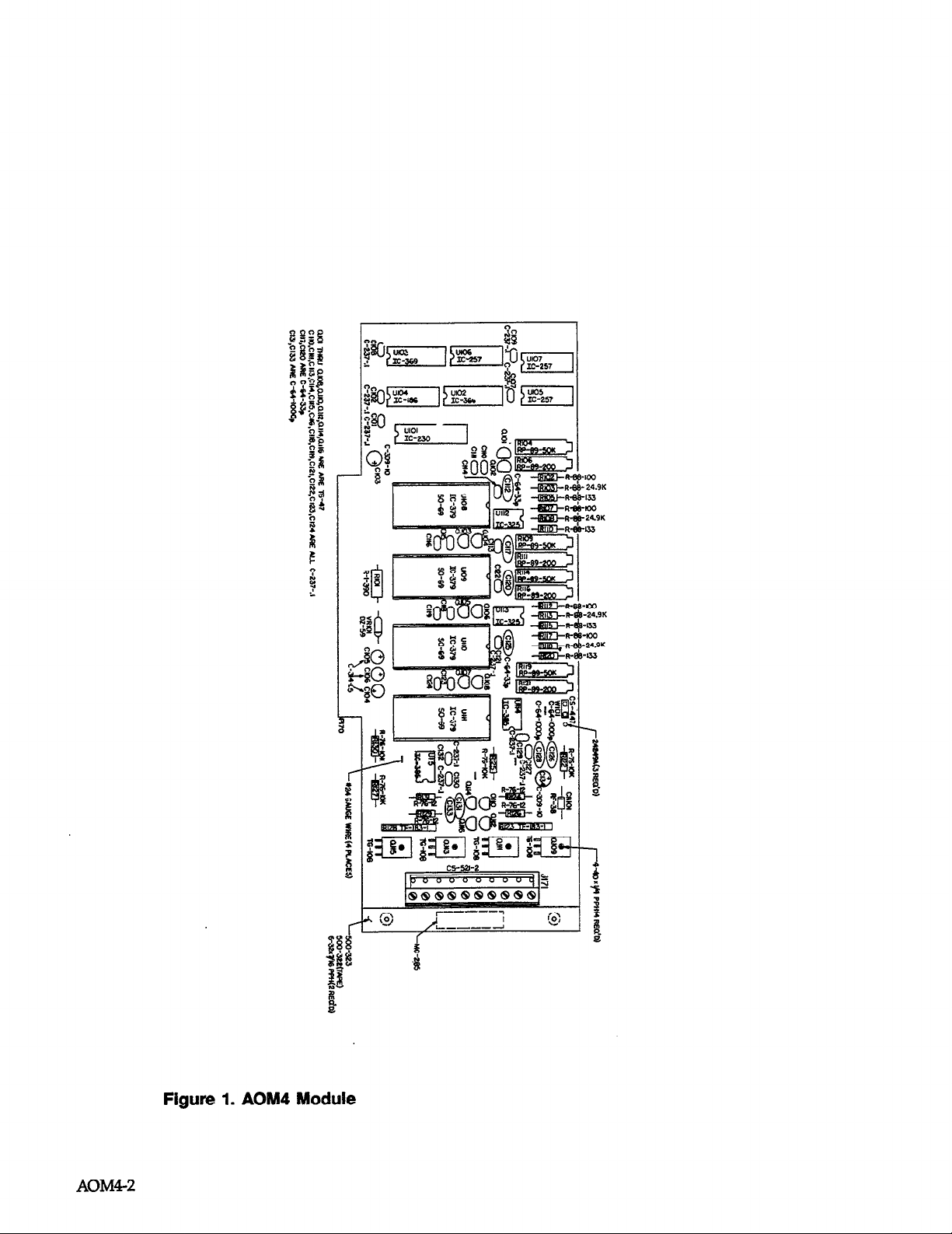
Figure 1. AOM4 Module
Page 3
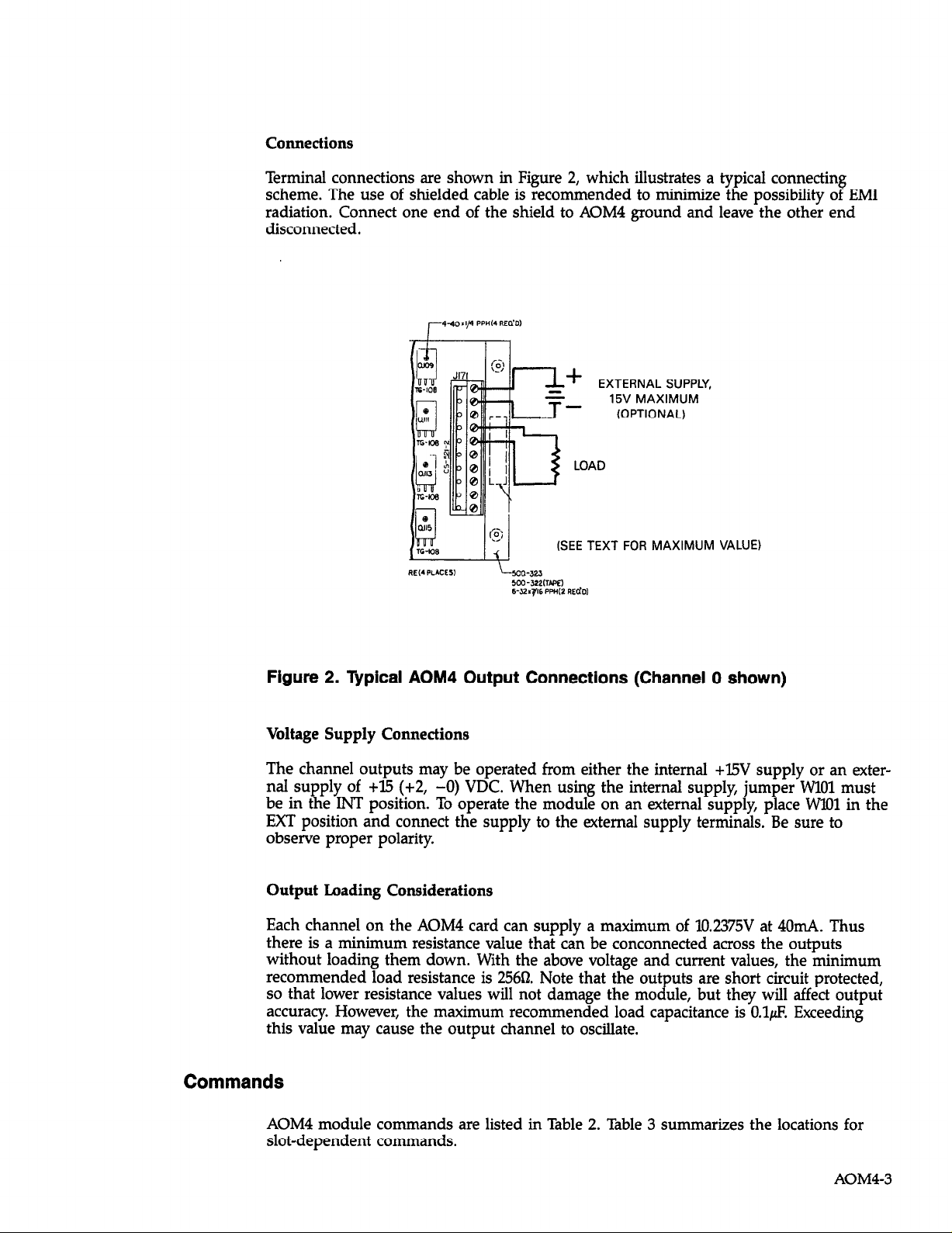
Connections
Terminal connections are shown in Figure 2, which illustrates a typical connecting
scheme. The use of shielded cable is recommended to minimize the possibility of EM1
radiation. Connect one end of the shield to AOM4 ground and leave the other end
disconnected.
IL!8
J---J-+
I“,” I
EXTERNAL SUPPLY,
(SEE TEXT FOR MAXIMUM
VALUE)
Figure 2. Typical AOM4 Output Connections (Channel 0 shown)
Voltage Supply Connections
The channel outputs may be operated from either the internal +l5V supply or an exter-
nal supply of +l5 (+2,
be in the INT position. To operate the module on an external supply, place WlOl in the
EXT position and connect the supply to the external supply terminals. Be sure to
observe proper polarity.
-0) VDC. When using the internal supply, jumper WlOl must
Output Loading Considerations
Each channel on the AOM4 card can supply a maximum of lO.2375V at 40mA. Thus
there is a minimum resistance value that can be conconnected across the outputs
without loading them down. With the above voltage and current values, the minimum
recommended load resistance is 25612. Note that the outputs are short circuit protected,
so that lower resistance values will not damage the module, but they will affect output
accuracy. However, the maximum recommended load capacitance is O.&S. Exceeding
this value may cause the output channel to oscillate.
Commands
AOM4 module commands are listed in Table 2. Table 3 summarizes the locations for
slot-dependent commands.
AOM4-3
Page 4
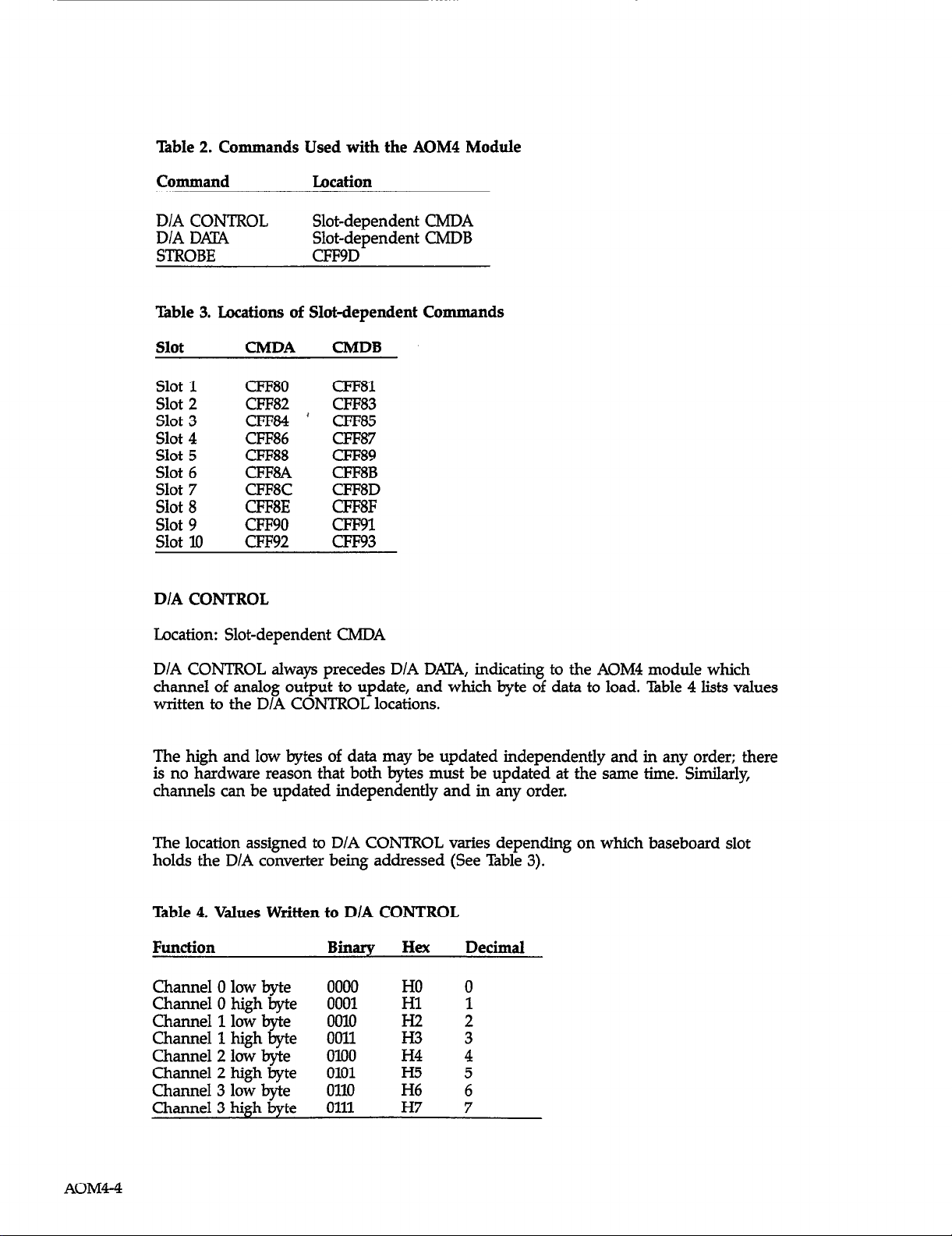
Table 2. Commands Used with the AOM4 Module
Command
D/A CONTROL
D/A DAL4
STROBE
Table 3. Locations of Slot-dependent Commands
Slot CMDA CMDB
Slot 1
Slot 2
Slot 3
Slot 4
Slot 5
Slot 6
Slot 7
Slot 8
Slot 9
Slot lo
D/A CONTROL
CFFSO
CFF82
cFF84
CFF86
CEE88
cFF8A
CFF8C
CFF8E
CFF90
CFF92
Location
Slot-dependent CMDA
Slot-dependent CMDB
CFF9D
Location: Slot-dependent CMDA
D/A CONTROL always precedes D/A DATA, indicating to the AOM4 module which
channe1 of analog output to update, and which byte of data to load. Table 4 lists values
written to the D/A CONTROL locations.
The high and low bytes of data may be updated independently and in any order; there
is no hardware reason that both bytes must be updated at the same time. Similarly,
channels can be updated independently and in any order.
The location assigned to D/A CONTROL varies depending on which baseboard slot
holds the D/A converter being addressed (See Table 3).
Table 4. Values Written to D/A CONTROL
Function Binary Hex
Channel 0 low byte 0000
Channel 0 high byte 0001
Channel 1 low byte 0010
Channel 1 high byte 0011
Channel 2 low byte 0100
Channel 2 high byte 0101
ChanneI 3 low byte 0110
Channel 3 high byte 0111
HO 0
Hl 1
H2 2
H3 3
H4 4
H5 5
iz; 7 6
Decimal
AOM4-4
Page 5

DIA Dp;TA
Location: Slot-dependent CMDB
D/A DATA is used to load data values into the D/A converter. This command should
always be preceded by D/A CONTROL, which selects the channel and the byte to be
loaded. The data must be separated into low and high bytes prior to loading, and each
byte must be prefaced by D/A CONTROL.
When the strobe feature is not enabled, the output of the converter is updated immediately. Thus, when the strobe is not used, the low and high bytes are updated independently. When the strobe is enabled, outputs are not updated until the STROBE
command is issued with the value 1 (to issue data).
To determine the digital value to input for a given voltage, it is necessary to know the
output range of the D/A converter. With a l2-bit digital converteI; there are 4096 possible voltage levels, specified with digital values O-4095. Therefore the actual voltage of
each step equals the range divided by 4095. For an input range of 0 to 10.237V the
voltage of each step is 10237V/4095 or 2.5mV: thus a BASIC formula for each voltage
value can be derived:
Where V is voltage and D is the digital value in counts loaded into the converter.
Similarly, the following BASIC equation determines the digital value to use when a particular voltage is required:
V
D= INT (
2.5 x 10-j
Again, D is the digital value, while V is the voltage.
The digital values may be separated into low byte (LB) and high byte (HB) values with
the following equations:
HB
= INT (D/256)
LB =(D/256-HB) l 256
STROBE
Location: CFF9D
The STROBE command is used to make possible the synchronous updating of two or
more analog output channels. STROBE is issued in three modes: strobe enable, strobe
disable and issue data. The STROBE feature must either be enabled or disabled at the
start of any program, or the D/A converters will not function (see Table 5).
When any strobe feature is disabled, all data given to a D/A converter is immediately
placed in that converter’s primary data latch, and the current output updated. The low
byte and high byte are thus updated asynchronously
AOM4-5
Page 6

When the strobe is enabled, no data is updated until the STROBE command has been
issued in the issue data mode. New data is placed in a secondary data latch within the
D/A converter. When the STROBE command (to issue data) is given, new data is released to the primary data latch, updating the voltage output, and old data in other channels is reissued, leaving the voltage output of these channels unchanged. The strobe is
completely flexible. Any amount of data-from a single byte to any number of channelscan be updated when the strobe is enabled.
To use the strobe, issue the strobe enable command early in the program. Use the D/A
CONTROL and D/A DATA commands to load the secondary latches of the appropriate
converters. This can be done as far in advance as required. To issue the new data, load
STROBE with 1 (to issue data), releasing all data loaded since the last issue data command and leaving unchanged the outputs of other channels.
The STROBE feature is global, affecting all D/A modules installed in the Series 500
simultaneously.
Table 5. Values Written to STROBE
Function BillarV
Strobe Enable 01000000 H40 64
Strobe Disable 10000000 H80 128
Issue Data 00000001 HO1 1
AOM4 Module Calibration
Calibration of the AOM4 module is very similar to the procedure used to calibrate the
AOMl. This module has only a single range, howevel; so the complexity is reduced
considerably. Figure 3 shows calibration adjustment locations for the AOM4 Program 1
lists a calibration program intended for use with this module.
1.
Place the module to calibrated in slot 5 of the system baseboard.
Unless an external voltage source is connected to the module, place the supply
2.
jumper in the internal position.
3.
Connect the DMM high (or current input)lead to the signal output terminal of the
channel being calibrated. Connect the DMM low signal lead to module ground.
4.
Select an appropriate function and range on the DMM. Remember that the AOM4
output signal is a voltage in the range of 0 to +10.2375V.
5.
Enter program 1 into the computer.
Run the program and follow the instructions given. The program will prompt for
6.
module type and output channel, and then display the correct offset and gain adjustment values in that order.
HeX Decimal
AOM46
Page 7

CHAN 0 OFFSET
CHAN 0 GAIN
CHAN 1 OFfWFT
CHAN 1 GAIN
&g-J
,, CHAN 2 GAIN
CHAN 2 OFFSET
CHAN 3 OFFSET
CHAN 3 GAIN
Figure 3. AOM4 Calibration Adjustments
AOM47
Page 8

Program 1. AOM4 Calibration
10 DEF SEG=&HCFFO:CLS
20 CA=&H88:CB=&H89:ST=&H9D
30 POKE ST,64
40 PRINT”1-AOM3”
50 PRINT”2-AOM4’
60 PRINTzINPUT ‘MODULE TYPE (1 OR 2)“;M
70 IF M<l OR M>2 THEN 60
80 IF M=l THEN M$=“AOM3”:R$=“CURRENT”
90 IF M=2 THEN M$=‘AOM4”:R$=“VOLTAGE”
100 PRINT “INSERT”;M$:“INTO SLOT 5”
110 PRINT:INI’UT “CHANNEL (0-3)“;CH
120 IF CH<O OR CH>3 THEN 110
130 PRINTPRINT “CONNECT DMM To CHANNEL’;CH
140 PRINT “SET DMM TO MEASURE”;R$
150 ON M GOSUB 300,320
160 POKE CA,2*CH:POKE C&LB
170 POKE CA,TCH+lzPOKE CB,HB
180 POKE ST,1
190 PRINTPRINT’ADJUST CHANNEL’;CH;“OFFSET FOR”; L$;“READING ON DMM”
200 INPUT “PRESS RETURN To CONTINUE”;A$
210 ON M GOSUB 310,330
220 POKE CA,2*CH:POKE CB,LB
230 POKE CA,2*CH+l:POKE CB,HB
240 POKE ST,1
250 PRINTPRINT’ADJUST CHANNEL”;CH;“GAIN FOR”;H$; ‘READING ON DMM”
260 INWT’TRESS RETURN To CONTINUE”;A!$
270 PRINTzINI’UT’AGAIN”;A!$
280 IF LEFl?§(A!$,1)=“Y” THEN 110
290 END
300 LB=1:HB=O:I$=“5@‘:RETURN
310 LB=255:HB=15:H$=“20.475m.A’:RETURN
320 LB==l:HB=O:I$=“2.5mV”:RETURN
330 LB=255:HB=15:H$=“10238V”:RETURN
Theory of Operation
The AOM4 schematic is located on drawing number 500-416.
The circuitry on the module can be divided into three groups: D/A conversion circuitry
for each of the four channels, command development circuitry, and data buffering
circuitry.
D/A conversion centers around the complete Y&bit D/A converters (AD567JN) one for
each channel of the module. These converter ICs are designated UlO8 through Ulll for
channels 0 to 3 respectively. The converters contain precision voltage references, high
speed analog switches, two levels of data latching, and a precision resistor ladder. Each
D/A converter is supplemented by a high-speed, high accuracy, operational amplifier,
Ull2A and Ull2B for channels 0 and 1, and Ull3A and Ull3B for channels 2 and 3
respectively.
Two potentiometers calibrate the gain and offset for each D/A converter: potentiometers
R106, Rlll and Rl21 calibrate the gain for channels O-3 respectively. Transistors QlO9,
AOM4-8
Page 9

4111, 4113 and 4115 are the output transistors for channels O-3, while QllO, 4112, 4114
and 4116 provide short circuit protection for those channels, Each op amp has a 0
OOluF capacitor in the feedback loop to prevent oscillation with large capacitive loads.
Components U102-U107 comprise the command development circuitry. A quad
transparent data latch, U102 (74LS75) stores the 3 bit command selected data (a number
between 0 and 7). This latch is refreshed by a negative pulse of the D/A CONTROL
command line (CMDA). CMDA is buffered and inverted by a hex inverter segment of
Ul.04 (74LSO4). U103, a binary-to-decimal decoder (74LS42), generates eight separate
command lines based on the 3 bit binary word from UlO2. The eight command lines
are then gated by quad OR gate segments of U105-Ul.07 to control data latching in
U108-Ulll.
The eight data lines are buffered by UlOl, an octal buffer (74LS244). The operation of
UlOl is controlled by the CMDA and CMDB lines through elements of U104 and U105.
UlOl will be enabled if either CMDA or CMDB is low.
AOM4 Specifications
Number of Channels: 4
Range of Output: 0 to 10.2375V
Resolution: 12 bits
Maximum Output Current: 4OmA
The AOM4 consists of 4 voltage-output channels. Each channel has a nominal output
voltage range of 0 to lO2375V with K&bit resolution. This corresponds to 2.5mV per
LSB. The output power supply can be provided either by the internal +l5V supply or
by an external +I!W supply. The output stage is short-circuit protected and can drive a
capacitive load of up to .l$.
AOM4-9
Page 10

I
0.101 THRU QUX~,~IK~,~~IZ,CUI~,QL~ ARE ARE TG-47
C IK).CIII.C~~~.C~~~.C~~~.CIL.C~B.C~~~.C~ZI~.C~~,CIW.C~~~ nRE ALL C-237-d
C117,ClX)ARE‘C-‘ii-33p
CuI,CI33 ARE C-~~-UDC’P
I
n,....
L W24 GA”GE WIRE (4 PLACES)
&QO-323
SDD-322 A
6-32x v2 PPH(2 RED!D)b
Page 11

I
iii
/!//i//l///l/
AOM4 SCHEMATIC DIAGRAM
AOM4-ll/AOM4-12
 Loading...