

Page 1

AOM2
High-Resolution Analog Output Module
The AOM2 High-Resolution Analog Output Module is available in two versions. The
AOM211 has one channel, while the AOM2/2 has two channels of analog output. Each
channel has a separate D/A converter. Unipolar and bipolar ranges are switch-selected
independently for each channel.
The converters provide true X-bit resolution with a maximum nonlinearity of stO.OOl5%
and low temperature coefficients. The AOM2 module also supports the system strobe
feature, which allows any number of output channels to be updated simultaneously.
Signal connections are made directly to screw terminals located on the module itself.
The AOM2 module may be placed in any slot in the baseboard. To install the module,
first turn off power and remove the top cover. Insert the module into the desired slot
with the component side facing the power supply. Place the AOM2 as far away from
the power supply as possible.
the possiblity of EMI radiation, never operate the system with the top cover removed.
User-Configured Components
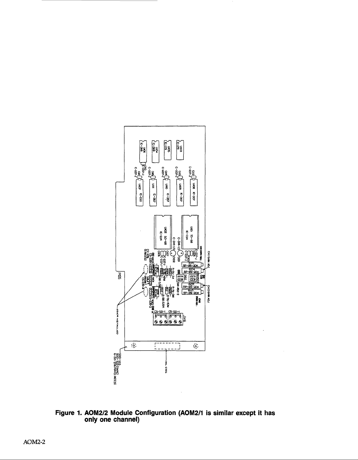
Each channel of the high resolution AOM2 module has a range selection switch, optional filter capacitor location, and screw terminal for signal connection. In addition,
channel 0 or channel 1 may be connected to the AN OUT baseboard path. See Table 1
and Figure 1 for a summary of user-configured components on AOM2.
The range-selection switch sets, Sl.01 and SlO2 (AOM2/2 only), can be set for two output ranges; *lOV and 0 to +lOV. Optional filter capacitors help preserve the converter’s
X-bit accuracy through the reduction of noise.
Screw Terminals for both converters are located on a single bank, with a common terminal for ground connection.
Jumpers select whether channels 0 or 1 are connected to the analog output signal path,
and allow shorting of the output resistor for each channel.
’ CAUTION: Always turn off the power when installing or removing modules. To avoid
Document Number: 500-930-01 Rev. C
AOM2-1
Page 2
r
AOMZ-2
Figure 1. AOM212 Module Configuration (AOMPM is similar except it has
only one channel)
Page 3
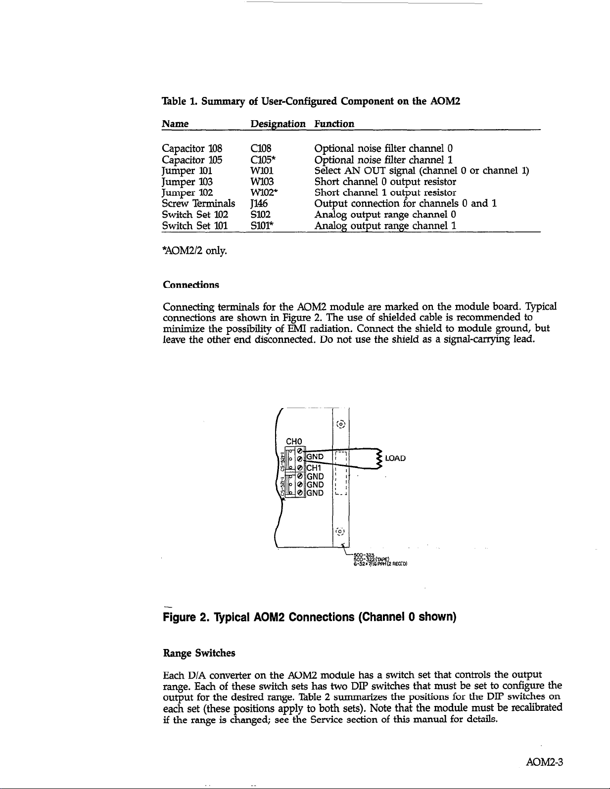
Table 1. Summary of User-Configured Component on the AOM2
Name Designation Function
Capacitor 108 Cl08
Capacitor 105
Jumper Il.01
C105”
WlOl
Jumper 103 wlo3
Jumper 102 wlo2*
Screw Terminals J146
Switch Set 102 slo2
Switch Set 101 s101*
Optional noise filter channel 0
Optional noise
filter
channel 1
Select AN OUT signal (channel 0 or channel 1)
Short channel 0 output resistor
Short channel 1 output resistor
Output connection for channels 0 and 1
Analog output range channel 0
Analog output range channel 1
*AOM2/2 only.
Connections
Connecting terminals for the AOM2 module are marked on the module board. Typical
connections are shown in Figure 2. The use of shielded cable is recommended to
minimize the possibility of EMI radiation. Connect the shield to module ground, but
leave the other end disconnected. Do not use the shield as a signal-carrying lead.
LOAD
Figure 2. Typical AOM2 Connections (Channel 0 shown)
Range Switches
Each D/A converter on the AOM2 module has a switch set that controls the output
range. Each of these switch sets has two DIP switches that must be set to configure the
output for the desired range. Table 2 summarizes the positions for the DIP switches on
each set (these positions apply to both sets). Note that the module must be recalibrated
if the range is changed; see the Service section of this manual for details.
AOM2-3
Page 4
Table 2. DIP Switch settings for Switch Sets SlOl and S102
Outuut Range 1 2
-10 to +lov*
oto +lov
*Factory default settings
Note: Switch settings are the same for both switch sets.
Preserving X-Bit Accuracy
With a &bit D/A converter, the value of a single voltage step is extremely small:
O.OOOl525V when the 0 to +lOV range is used. Electrical noise or temperature drift can
easily obscure such a small voltage change, reducing accuracy dramatically. The following sections suggest measures to maintain the accuracy of the converter.
Noise
Signal changes at the microvolt level are extremely difficult to transmit over wires even
a few inches long. Therefore, good signal connection practices should always be observed. The length of connecting wires should be minimized, and these wires should never
run alongside AC power lines. In addition, shielded cable should always be used, with
the shielding connected to the ground terminal of the module.
If noise remains a problem, output filters for each channel can be installed on the
module itself.
Open
Closed
Closed
Open
Cl08 provides filtering for channel 0, while Cl05 is for channel 1. The required
capacitor value for a given bandwidth can be calculated as follows:
1
=-
C
P?rRf
Where C is in farads, f is in hertz and R is in ohms. Note that large capacitor values,
while providing greater noise rejection, will reduce output bandwidth accordingly. For
example, assume that the bandwidth is to be restricted to 3OHz. The required capacitor
value is (with a channel output resistance of lkn):
1
c=
6283(30)
C = 5pF
Note: Do not install filter capacitors with output resistors jumpered.
Analog output
A direct connection between the output of channel 0 or channel 1 and the AIM1 is
made through the baseboard connector’s AN OD’T signal path. An on-card Berg jumper
AOM2-4
Page 5
(WlOl) is provided, so the connection can be defeated if noise from this source is
experienced. To connect channel 0 to the AN OUT path, place the WlOl jumper on the
middle two pins. To connect channel J, place the jumper on the left two pins. Place the
jumper on the right two pins to leave both channels disconnected.
Temperature Drift
D/A converters, like many electrical components, are sensitive to temperature change.
The AOM2 converters are designed with extremely low temperature coefficients (low
sensitivity to temperature changes); however, an attempt should be made to maintain
the operating environment near room temperature.
The converter has been calibrated to be accurate when operating. Because the
temperature of the device is higher when it is operating than when it is not in use, no
critical operations should be performed until the system has been on for at least five
minutes.
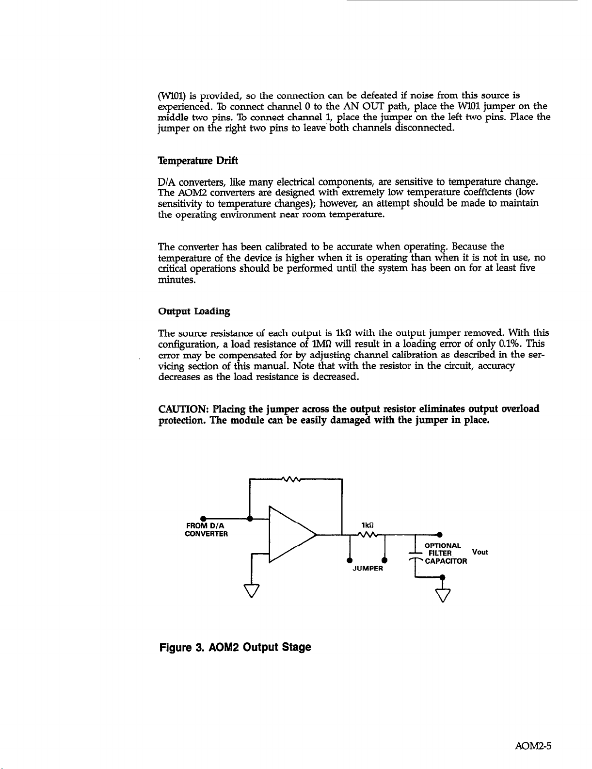
Output Loading
The source resistance of each output is lkQ with the output jumper removed. With this
configuration, a load resistance of IMQ will result in a loading error of only 0.1%. This
error may be compensated for by adjusting channel calibration as described in the ser-
vicing section of this manual. Note that with the resistor in the circuit, accuracy
decreases as the load resistance is decreased.
CAUTION: Placing the jumper across the output resistor eliminates output overload
protection. The module can be easily damaged with the jumper in place.
0
FROM D/A
CONVERTER
A
1ki-l
JUMPER
Figure 3. AOM2 Output Stage
AOM2-5
Page 6

Commands
AOh module commands are listed in Table 3. Table 4 summarizes the locations for
slot-dependent commands.
Table 3. Commands Used with the AOM2 Module
Command Location
D/A CONTROL
D/A DAE4 STROBE
Location: CFF9D
Table 4. Locations for Slot-dependent Commands
SlQt CMDA CMDB
Slot 1
Slot 2
Slot 3
Slot 4
Slot 5
Slot 6
Slot 7
Slot 8
Slot 9
Slot lo
D/A CONTROL
Location: Slot-dependent CMDA
D/A CONTROL always precedes D/A DATA, indicating to the AOM2 module which
channel of analog output to update, and which byte of data to load.
CFFSO
CFF82
cFF84
CFF86
EE
CFFSC
CFFSE
CFF90
CFF92
Slot-dependent CMDA
Slot-dependent CMDB
CFF81
CT%83
CFF85
CFF87
CFF89
CFF8B
CFFSD
CFFSF
cFF91
CFF93
AOM2-6
The high and low bytes may be updated independently and in any order; there is no
hardware reason that both bytes must be updated at the same time. Similarly, channels
can be updated independently and in any order.
Note that the byte/channel selection is retained by the module; if a single byte/channel
will be updated several times in succession, the D/A CONTROL command need not be
reissued.
Table 5. Values Written to the D/A Control Location
Function
Channel 0 Low Byte
Channel 0 High Byte
Channel 1 Low Byte
Channel 1 High Byte
Note: AOM211 has channel 0 only.
Binary Hex Decimal
0000
0001
0010
0011
HO 0
Hl 1
H2 2
H3 3
Page 7

D/A DATA
Location: Slot-dependent CMDB
D/A DAYI?4 is used when loading actual data values into the D/A converter. This com-
mand should always be preceded by D/A CONTROL, which selects the channel and
the byte to be loaded. The data must be separated into low and high bytes prior to
loading, and each byte must be prefaced by D/A CONTROL. If a byte/channel will be
updated repeatedly, D/A CONTROL need not be reissued.
When the strobe feature is disabled, the output of the converter is updated immediately. This implies that the low and high bytes are updated independently. When the
strobe is enabled, no outputs are updated until the STROBE command is issued in the
issue data mode.
The digital value loaded into the converter varies according to the output range selected
via switch sets SlOlSlB2. To determine the digital value to input for a given voltage, the
output range must be known. With l&bit conversion, there are 65,536 possible voltage
levels, specified with digital values O-65,535. The voltage of each step equals the range
divided by 65,535. For an input range of 0 to lov, for example, the voltage of each step
is 10/65,535, or 0.0002525. A formula for each voltage range is provided below.
Table 6. Digital Value to Volts
Output Range Voltage
0 to +lov V = D * 0.0001525
-10 to +lov
v= -lo + (D * 0.0003050)
Where V is volts, and D is the digital value loaded into the converter. Similarly, the
following equations determine the digital value to use when a particular voltage is
required:
Table 7. Volts to Digital Value
Output Range
oto
+lov
-10 to +lov
Digital Value
D = INT(V/O.OOOl525)
D = INT(V10.0003050) + 32768
STROBE
Location: CFF9D
The STROBE co
mmand is used to make possible the synchronous updating of two or
more analog output channels. STROBE is issued in three modes: strobe enable, strobe
disable, and issue data. The STROBE feature must either be enabled or disabled at the
start of any program, or the D/A converters will not function.
AOh42-7
Page 8
When the strobe feature is disabled, all data given to a D/A converter is immediately
placed in that converter’s primary data latch, and the voltage output updated. The low
byte and high byte are thus updated asynchronously.
When the strobe is enabled, no data is updated until the STROBE command has been
issued in the issue data mode. Instead, new data is placed in a secondary data latch
within the D/A converter. When the STROBE command (to issue data) is given, the
new data is released to the primary latch, updating the voltage output, and old data in
other channels is reissued, leaving the voltage output of these channels unchanged.
The strobe is completely flexible. Any amount of data - from a single byte to any
number of channels - can be updated when the strobe is enabled.
To use the strobe, issue the strobe enable command early in the program. Use the D/A
CONTROL and D/A DATA commands to load the secondary latches of the appropriate
converters. This can be done as far in advance as required. To issue the new data, load
STROBE with 1 (to issue data), releasing alI data loaded since the last issue data com-
mand and leaving unchanged the outputs of other channels. See ‘Iable 8 for a summary
of values written to the STROBE location.
The STROBE feature is global, affecting all D/A modules installed in the Series 500.
Table 8. Values Written to STROBE
Function Binary HeX
Strobe Enable 01000000 H40 64
Strobe Disable 10000000 HSO 128
Issue Data 00000001 HO1 1
AOM2 Module Calibration
The AOM modules should be calibrated whenever the range is changed. Because a considerable amount of programming is necessary, a program is presented in this manual
as an aid in calibrating these modules. Program 1 is intended for the AOM2. Use the
following procedure when calibrating this module.
1. Place the AOM module to be calibrated in slot 5. Set the output range as indicated in
Table 9.
2. Enter the program into the computer.
3. Connect the DMM high input lead to the signal terminal of the channel being
calibrated. Connect the DMM low lead to module ground. For maximum accuracy,
connect
4. Run the program and follow its instructions. Refer to Figure 4 for adjustment locations. Make sure the output range of the module is set correctly. The program will
prompt with the correct range switch settings.
5. Repeat the procedure as necessary with the remaining channels.
the usual load resistance between the signal terminal and ground.
Decimal
AOM2-8
Page 9

CJXEl10kldNfl
m..... ^ .I.. _^ ^
SklOli3VdV3 kEllllzl
Page 10

Table 9. AOM2 Output Range
Range
oto +lov
-10 to +lov
Note: 0 = Open, C = Closed
SlOl = Channel 1
S102 = Channel 0
Program 1. AOM2 Calibration
10 DEF SEG = &HCFFO: CLS
20 CA = &H88: CB = &H89: ST= &H9D
30 POKE ST, 64
40 HUNT "INSERT AOM2 INTO SLOT 5"
50 PRINT: JNnJT%oM2 CHANNEL (o-y; CH
60IFCH<OORCH>lTHEN50
70 PlUNT PRINT "CONNECT DMM TO CHANNEK'; CH
80 PRINT: l3UNT "RANGE SWITCH POSITIONS"
9OpRINT"lY
loo PRlNT "10 To +lov c 0"
llOl?RmY2-1om +1ovoc
120 PRlNT: INPUT"RANGE (l-2)"; R
l30PRlNTzIFR< lORR>2THENl20
140 ON R GOSUB 280, 300
150 POKE CA, 2*CH: POKE CB, LB
IL60 POKE CA, 2*CH + 1: POKE CB, HB
170 POKE ST, 1
180 MUNTz PRINT'ADJLJST
ON DMM"
190 INPUT 'TRESS RETURN To CONTINUE"; A$
200 ON R GOSUB
210 POKE CA, 2*CH: POKE CB, LB
220 POKE CA, 2*CH + 1:POKE CB, HB
230 POKE ST, 1
240 PRINT: PRINT'ADJUST
DMIW
250 INPUT'TRESS RETURN TO CONTINUE"; A!$
260 PRINT: INF'UT'AGAIN"; A$
270 IF LEF'I!$ (A!$,l)
275 END
280 LB = 0: H-B = 0: r$ ="0.000":RETuRN
290 LB = 255: HB
300 LB = 0: HB =
310 LB =0: HB =0: H$ ="-10.000": RETURN
slcl1
1 2
E :
290, 310
= 255: H$ E"9.999": RETURN
328: L$ ="O.OOO": RETURN
slo2
CHANNEJZ'; CH;"OFFSET FOR "; L$;"VOTII' READING
CHANNEL!'; CH;"GAIN FOR"; H$" VOLT READING ON
="Y" THEN 50
AOM2-10
Page 11
Theory of Operation
For the following description, refer to schematic number 500-226.
The circuitry on the AOM2 falls into three functional groups: the components providing
D/A conversion and data-latching capabilities for each channel, the components for
command development, and a single IC which buffers the data lines.
A hybrid, 16-bit D/A converter is provided for each channel on the AOM2 module.
These converters, designated UlOl and U102 on the schematic diagram, are complete,
containing precision voltage references, output amplifiers, and data latches. Four S-bit
transparent data latches, Ul.O8-Ulll (74LS373), provide a secondary level of data latching, supporting the system strobe feature. The enable line for each of these latches is
driven by one of the four commands set up by U104.
Potentiometers RlOl, RlO4, RlO7 and RllO calibrate the gain and offset for the D/A converters (RlO4 and RlO’7 calibrate the gain, RlOl and Rll.0 the offset). DIP switches SlOl
and S102 set the output ranges independently for the two converters.
W102 and WI03 allow control of output protection. For added output protection, place
the jumper in the PROT position. WlOl is used to select the channel (0 or 1) to be
routed to the AN OUT signal path. A third position is intended to hold the jumper
when neither channel is to be routed.
Commands are decoded by components U103U106. UlO6 is a quad transparent data
latch (74LS75) which stores the 4 bit command select data. U106 is refreshed by the
negative transition of command line A (CMDA, D/A CONTROL). A NOR gate segment
of U103 (74LSO2) buffers and inverts CMDA before it reaches U106.
UlO4 is a one-of-ten binary to decimal decoder (74LS42) that generates four separate
command lines based on the 4 bit command word stored in U106. These four command
lines enable the secondary data latches of the D/A converters, and are gated by CMDB
(D/A-l6 DAL4) in quad NOR gate segments of UlO5 (74LSO2). Buffering of the eight data
lines is accomplished by U107 (74LS245), configured as a buffer.
AOh&II
Page 12

AOM2 Specifications
Output channels: 2 (1 on the AOM.211)
Output ranges: *lW, 0 to +lUV, switch selectable for each channel
Resolution: 16 bits, 1 part in 65,536
Nonlinearity: f0.003% of ES. (*l lsb)
Output impedance: 0.1
Load characteristics: 2khl min, lOOOpf max short-circuit protected
Slew rate: 0.2Vlflec
Settling time: 2Opsec to 0.006% of ES. transition
Temperatuw coefficient: ’
Gain:
0.0007%/°C of ES., 0 to +lUV range
0.0009%/°C of F S *
offset:
O.O009%/“C of ES., 0 to +lOV range
O.OOll%l°C of ES: -10 to +lUV range
*Full scale for bipolar ranges is defined as -V, to +V,
-10 to +lOV range
* *I
AOMZ-12
Page 13

UK@ c-357
CH I GAIN ADJ< CH 0 GAIN ADJ
Jl46
I
:-76-M
R-76-3M
\ \
USER INS’J-ALLEO
Page 14

Di.
E
D4
E2
-07
PI26 1 WV23 1
RI!3 I
-- *‘* ’
A
I
I I
I
B - I
I
I
c
,. ‘:
,: *
I
A
I
-
E
I
F I
AOM2 SCHEMATIC DIAGRAM
.G
AOMZ-l51AoM2-16
 Loading...