

Page 1
IBIN-A, IBIN-LP PC Interfaces
The IBIN-Ainterface plugs into any slot in an IBM I’C/XT/AT/386/486 Personal System/2 Models 25,
30, or compatible, and serves as an interface between the computer and the Series 500. In addition, the
interface card hosts other functions ccmmon to the Series 500 system: the programmable interval timer,
and the switch selectable wait state generator.
The IBIN-LP is a low-power version of the standard IBIN-A interface which was designed for use in
lap-tops or other computers which cannot supply enough current in their expansion slots to power the
standard IBIN-A. The IBIN-Ll’ achieves its reduced power requirement through the use of low-power
components. Physically, the IBIN-A and IBJN-Ll’ are identical, and share the same component layout
and designations. Instructions for installation and use are also the same for both cards.
The programmable interval timer can be used to time events, create software delays, and generate periodic interrupts in the PC. The timer consists of three independent 16-bit counters with a resolution of
one microsecond. The three counters can be cascaded to create longer timing intervals.
The wait state generator provides compatibility with many computers which use non-standard bus
timing or processor speeds.
Configuring the IBIN-A Interface Card
User configurable features of the IBIN-A interface include an address mapping switch, a PC bus wait
state generator switch, and a removable cable for connecting the interface card to the Series 500 system.
In addition, there are several jumpers that can be used in special applications to achieve additional flexibility
Switch Sl selects the address range of the interface in the system memory map. This switch is normally
set for a starting location of hex CFFSO (the factory default), but can be configured over the full one
megabyte addressing range of the PC. The switch setting determines the most significant 8 bits of the
Series 500’s address region, which is 4K in size. The upper 128 bytes of memory in this 4K area contain
the active memory locations used to communicate with the Series 500.
Functionally, switch set Sl consists of two groups of four switches. Switches l-4 control which 64K segment of memory the IBIN-A resides in. For any 64K segment, the second address digit can be set from
0 through F (hex). The last three digits of the address are hard-wired to “F80”. This permits the interface
address to be set to the top 127 bytes of consecutive 4K blocks of memory within any 64K segment.
Document Number: 501-910-01 Rev. D
IBIN-
Page 2
Table 1. IBIN-A Address Switch Setting Information
64K
Segment 1 2
Fxxxx off off off off xFF80
Exxxx off off
Dxxxx off off on
cxxxx off
BXXXX
Axxxx off on
9xxxx off on on off x9F80 off on on
8xxxx off on on on
As an example, to set the interface to respond at address CFF80 you would set the switches 1 through
8 as follows:
1 2 3 4 5 6 7 8
off off on on
An address range which is almost universally available regardless of computer is CAF80 through
CFFSO. Note that many of the possible addresses will conflict with other hardware, RAM, or ROM al-
ready in the computer, so the practical range of addresses is fewer than the switches provided for. However, there will normally be many more addresses available than are actually needed.
off on off off xBF80 off on
off on on XCFSO off off on on
3
off on xEF80 off off off on
off on XAFSO off on off on
4
off xDF80 off off on off
off off off off
4K
Region 5 6 7
off off off off
off off
XSFSO off on on on
8
off
Hardware options for the PC or AT, such as fixed disks, enhanced graphics adapters, and expanded
memory occupy portions of the PC memory map, and preclude using the same addresses for the
IBIN-Ainterface. Memory conflicts occur when the computer attempts to read an address occupied by
more than one piece of hardware. These problems can be manifest as error messages at boot-up, or failure of the computer or data acquisition system to operate properly. If this occurs, examine the memory
usage of all hardware in your computer, and make changes where necessary. Usually, changing the address of the IBIN-A interface is all that is required.
The following is a map of common memory usage in a standard AT or 386:
FOOOO-FF’FFI? Universally used for ROM BI05. Interface should generally not be addressed to this
block.
EOOOO-EFFFF: Used by some 16 bit VGA cards. May be used by Lotus-Intel-Microsoft “EMS” expansion
memory. Also reserved for system use in AT-class computers. If no functions or hardware use all these
addresses, area may be used for IBIN-A interface.
DOOOO-DFFFF: May be used by Lotus-Intel-Microsoft “EMS” expansion memory. This page is often the
location of a LAN card. If no functions or hardware use all these addresses, area may be used for
IBIN-A interface.
IBIN-
Page 3
COOOO-CFFFF: Lower portion of this page typically occupied by Fixed disk ROM B105 and Video BI05
ROM. Interface can be set to use CAFSO through CFFSO for most systems.
AOOOO-BFFFF: Universally used by VGA, EGA, or CGA. Interface cannot be set to this block. This area
not normally available for interface.
00000-9FFlP RAM space from OK to 640K. This area should not be used for interface.
You should have no technical difficulty finding usable addresses, although you may have to do some
research to find out what addresses are free in your computer. Normally, CFFSO will be compatible with
any computer and installed hardware.
Memory Conflicts
In very rare cases, a system may be loaded with options which use addresses in the COOO, DOOO, and
EOOO address blocks. Increasingly, hardware and software options such as EMS memory, “shadowed
ROM BIOS”, and VGA cards are being added by computer manufacturers or end users. These options
can monopolize the one or two complete pages of memory. If the COOO, DOOO, and EOOO pages are all
used, the process of integrating the computer and IBIN-A becomes much more complex. Finding a free
address in such computers can require trial and error testing, a search through the computer documentation, or a call to the computer manufacturer. The IBIN-A installation may ultimately result in a sacrifice of some of the computer’s speed, enhancements, or overall performance. Examples include:
1. I6-BIT VGA VIDEO ADAPTERS -Some VGA adapters feature 16-bit addressing, and use addresses up to E000:O. These cards can be identified by the presence of a second AT-type card edge
connector behind the main card-edge connector. Memory usage will vary as the adapter enters and
leaves its various display modes. When the card permits, the solution is to reconfigure the VGAfor
&bit operation by setting switches or running utility software. This may cause a reduction in video
update speed or loss of some unique resolution modes or enhancements designed in by the VGA
manufacturer.
2. EMS MEMORY - Expanded memory is also called “paged” memory. EMS was originally designed to provide PC/XT computers with up to eight or more megabytes of RAM, even though the
8088kP can address only 1 Mbyte of memory. EMS can also be used in 286- and 386.based computers. Most EMS boards require a free, contiguous 64k address space which acts as a window into all
the EMS memory. The solution is to install the EMS software to specifically exclude the space that
the IBIN-A requires. Instructions for excluding a particular range of segment addresses for an EMS
page are given below for three popular 386 expanded memory manager packages. Add the exclude
statement to the CONFIG.SYS declaration which corresponds to the memory manager you are using.
IBIN-
Page 4
386 Expanded
MeIlKlly Minimum
Manager Exclude Statement CONFIGSYS Declaration Exclusion
DOS 5.0’s X = CFOO-WOO
EMM386
Qualita’s
386 MAX
Quarterdeck’s EXCLUDE = CFOO-CFFF DEVICE = QEMMSYS 4K
EXCLUDE = CCOO-DO00 DEVICE = 386MAX.SYS 16K
DEVICE = EMM386.EXE
4K
QEW
Each of the above examples assumed that the IBIN-A address switch is set to the default CFFS hex.
Note: an exclude statement is required because the IBIN-A cannot be detected by a memory manager. A memory manager is likely to take all unexcluded memory blocks for its own use.
3. “SHADOWING” -This technique copies system ROM BIOS or VGA BIOS information stored in
relatively slow system ROM chips to faster-reading RAM, usually in the DO00 or EOOO pages. Once
in RAM, the information can be read more quickly by the computer’s pP, resulting in a faster system. By itself, shadowing does not necessarily consume all the available high memory addresses.
However; a system which combines shadowing, 16-bit VGA, and EMS memory may leave no ad-
dresses vacant for the IBIN-A. Consult your computer documentation for instructions on disabling
the shadow RAM.
Any of these problems require a careful study of the documentation for the affected hardware to determine how memory is allocated in a specific computer, and what steps may be available to solve the
problem. Keithley can offer specific suggestions on setting up the IBIN interface, but users may have to
contact vendors of the other equipment to find a complete solution.
IBIN-
Page 5
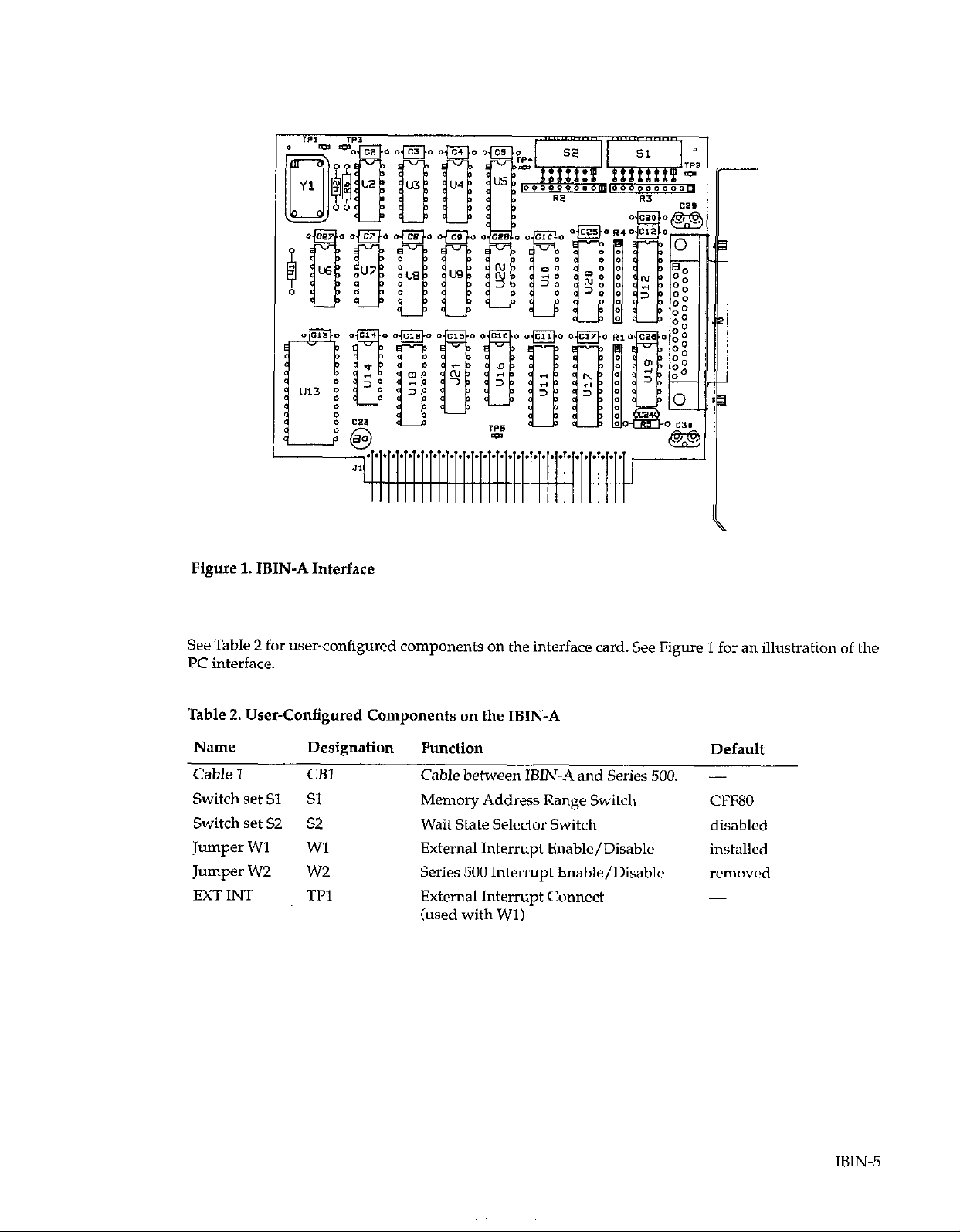
Figure 1. IBIN-A Interface
See Table 2 for user-configured components on the interface card. See Figure 1 for an illustration of the
PC interface.
Table 2. User-Configured Components on the IBIN-A
NiXme Designation
Cable 1 CBl
Switch set Sl Sl
Switch set 52 S2
Jumper Wl Wl
Jumper W2 W2
EXT lNT
TPl
Function
Cable between IBIN-A and Series 500.
Memory Address Range Switch
Wait State Selector Switch
External Interrupt Enable/Disable
Series 500 Interrupt Enable/Disable
External Interrupt Connect
(used with Wl)
Default
CFFSO
disabled
installed
removed
IBIN-
Page 6

Installing the IBIN-A Interface Card
CAUTION: Turn off the power before installing or removing the interface card in the computer.
The IBIN-Ainterface is installed into expansion slots inside the PC system unit. It may be installed into
any vacant slot of the computer.
Install the IBIN-A into an expansion slot as follows: Make sure the PC is turned off, and unplug the
power cord. Consult the computer manufacturer’s documentation for instructions on opening the computer. Remove the outer case and any other covers to gain access to the computer’s expansion slots.
A rear panel opening is provided at the end of each expansion slot for mounting I/O connectors. If a
slot is unused, then this opening will be covered by a metal plate held in place by a screw on top of the
plate. Remove the retaining screw and cover plate from the desired expansion slot. Be very careful not
to drop the retaining screw into the computer, it may be difficult to retrieve.
Carefully insert the IBlN-A into the expansion slot, fitting the DB25 connector through the rear panel
operating so that the mounting bracket is in the correct position to be fastened securely by the retaining
screw removed earlier. Insert the card edge into the mother board card edge receptacle. With the board
firmly in place, install and tighten the retaining screw. Finally, attach the interfacing cable to the connector (JZ) on the interface card at the rear of the computer. The cable connecting the PC to the Series 500
is a shielded 23-contact cable. The cable should be attached to the baseboard of the Series 500 unit. Never strain the connection between cable and connector. The outer end of the cable should be plugged into
the connector (Jll7) on the rear panel of the Series 500 base unit. This connection should be made with
power to the Series 500 turned off. Avoid entangling the interface cable in 60 cycle AC power lines.
Software Installation and Wait States
Switch SW2 enables and disables the wait state generator. For most computers, this feature can be left
disabled (all wait state switches set to OFF). The need to change the wait state switches will become evident for a given computer if certain problems arise during installation or operation of software. For instance, some PC compatibles running at rates higher than 8MHz will not work properly with the Series
500. One indication would be if the INSTALL program supplied with KDAC500 aborts or issues error
messages such as “Interface not found” or “Can’t trigger interrupts”. Another indication would be if
KDAC500 installs correctly, but later yields incorrect data during acquisition.
If you are running a compatible computer which uses non-standard bus or processor speeds, you
should try installing KDAC500 even if you are planning to use a software package other than
KDAC500. If any timing problems exist, you may then add wait states to see if the problem can be COTrected.
To change the number of wait states, see Figure 1 to locate switch 52. There are seven switches on the
52 switch set. In order to add one wait state to the bus you would set switch 1 to on. Reinstall the
Keithley software, and then re-run your test. If the system still does not function, try setting both 1 and
2 on. Continue in this manner until all switches are on. Run the INSTALL software supplied with the
Keithley software each time you make a change.
IBIN-
Page 7

If you are using a third-party software package, consult its documentation for installation details.
Interrupt Selection
The interrupt levels, in order of priority, are shown in the following chart. Interrupt usage is controlled
through software;
PC or XT (8088 or 8086)
CLOCK CLOCK
LEV2
LEV3 LEV3
LEV5
See the installation section of the KDACSOO software manual for complete instructions on running INSTALL with command modifiers which select other interrupts.
Jumper Settings for Selection of Interrupt Source
Method of Interrupt
Generation
On board timer 8254 (Default)
External interrupt applied to
TPl
Interrupt generated by a Series
500 option module
AT (80286) or 80386
LEV9
LEV5
Jumper Wl Jumper W?. Note:
Installed
Removed Removed Allows synchronization to an
Removed
Removed
Installed 500.TRGl is currently the only
Default
external time base.
module which can generate an
interrupt.
Hardware installation is completed, Reassemble the computer in reverse order of disassembly, being
careful that no screws or other hardware have dropped into the system. Plug the computer’s power
cord back in.
Interrupt Conflicts
The IBIN-A interface can use the NM1 (Non-Maskable Interrupt), CLOCK, INT2, INT3, or lNT5 for interrupt-driven data acquisition under Keithley’s KDAC500 software. The selection is made during the
installation of the software, with NM1 being the default. The interrupts are activated by the CALL INTON command. Third-party software packages can have their own interrupt strategies, but quite often
use CLOCK.
Keithley recommends using the NM1 because the NM1 takes priority over all other system interrupts
and events, and gives the most precisely-timed acquisition. The NM1 was originally designed for use
with memory parity checking. However, some hardware accessories also use the NM1 for other tasks.
Among these are “auto-switching” EGA cards and the dynamic RAM refresh of some Zenith comput-
IBIN-
Page 8

em Such systems will operate properly until the user runs a data acquisition program including a
CALL INTON command, at which point a “Parity Check” or other error results.
There are two solutions to making the IBIN-A work in systems which use the NM1 for other functions.
One is to disable the other hardware’s use of the NMI. Some EGA cards have a switch or programmable
register to disable use of the NMI. This is not possible with all hardware, and the second solution is to
simply install the Keithley software to use another of the available IBIN-A interrupts.
Interrupt Usage in PCs and ATs
Keithley’s KDAC500 can be installed to use the NMI, CLOCK, INT2, INT3, or INT5 interrupts. The actual choice of interrupt depends on other hardware which may be in the system.
The following table summarizes inteirupt usage in XT-type computers:
INT
Application
0 Timer
1
Keyboard
2 Reserved
3
Secondary asynch adapter (COM2)
4
Primary asynch adapter (COMI)
5 1 Iard disk controller
6
Floppy disk controller
7
Printer (not used in most machines)
The following rules can be defined for XT computers:
1. Use NMl for the most precisely timed data acquisition.
2. If NM1 causes problems in the system, consider INT2, INT3, or lNT5 in that order.
3. If the XT contains a hard disk, lNT5 cannot be used.
4. If the system contains COMl and COM2, INT3 cannot be used. A serial mouse and an available
COM port probably eliminate lNT3. A bus mouse and one COM port may leave lNT3 available. A
LAN adapter probably uses INT3.
5. If there are no other adapter boards in the computer, lNT2 is probably available, although some
multi-function I/O boards may use INT2.
6. Use CLOCK as a last alternative.
IBIN-
Page 9
The following table summarizes interrupt usage in PC/AT computers:
INT Application
Timer
Keyboard
Orred summary of INTB-INT15
Secondary asynch adapter (COM2J
Primary asynch adapter (COMl)
Parallel port 2 (LPT2)
Floppy disk controller
Parallel port 1 (LPTl)
This table provides these guidelines for AT computers:
1. Use NMl for the most precisely timed data acquisition.
2. If using NM1 causes problems in the computer, consider INT2,lNT3, or INT5 in that order.
3. On a true AT compatible, INT2 is not available. However, many AT compatibles do not use INT2 as
the original IBM PC/AT did. In this case, INT2 may be usable.
4. If the computer contains COMl and COM2, INT3 cannot be used. A serial mouse and a COM port
probably make lNT3 unavailable. A bus mouse and a single COM port probably mean INT3 is
available. A LAN adapter probably uses INT3.
5. If the computer contains no other adapter boards, then INT5 is probably available.
6. While lNT5 is assigned for printer use, there seem to be few printer adapters that really use interrupts. In fact, the DOS print spooler does not support it. Therefore, lNT5 is usually a workable alternative (provided something else doesn’t use it).
7. Use CLOCK as a last alternative.
In summary, use NM1 if possible. To use INT2,lNT3, or INT5, first determine what other options may
be using these interrupts and choose accordingly. The ultimate confirmation of whether a given interrupt is suitable may require trying it. The usual symptoms of interrupt conflicts are POST error messages, bad data, or a locked-up computer. Since INT2,lNT3, and INT5 are used by various hardware
options, problems with serial ports, fixed disks, or printer ports may also occur, although they have
been rare. These symptoms will usually appear immediately when the system is turned on, or soon af-
terward. Use CLOCK as a last alternative.
Programmer Model for the Memory Map
A summary of memory locations used with the interface card is given in Table 3. These addresses correspond to the “Command A” and “Command I%” functions which are associated with each module in
the Series 500 module library. Note that some modules also use “Command C” and “Command D” ad-
IBIN-
Page 10
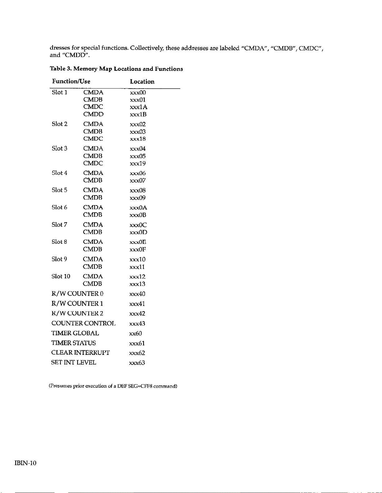
dresses for special functions. Collectively, these addresses are labeled “CMDA”, “CMDB”, CMDC”,
and “CMDD”.
Table 3. Memory Map Locations and Functions
Function/Use Location
Slot 1
CMDA
CMDB
CMDC
CMDD
Slot 2
CMDA
CMDB
CMDC
Slot 3
CMDA
CMDB
CMDC
Slot 4
CMDA
CMDB
Slot 5
CMDA
CMDB
Slot 6
CMDA
CMDB
Slot 7
CMDA
CMDB
Slot 8
CMDA
CMDB
Slot 9
CMDA
CMDB
Slot 10
CMDA
CMDB
R/W COUNTER 0
R/W COUNTER 1
R/W COUNTER 2
COUNTER CONTROL
TIMER GLOBAL
TIMER STATUS
CLEAR INTERRUPT
SET IN-I’ LEVEL
xxx00
XXX01
XXXlA
xxxlB
xxx02
xxx03
XXX18
xxx04
xxx05
xxx19
xxx06
xxx07
XXX08
xxx09
xxxOA
xxxOB
xxxoc
xxxOD
xxxOE
xxxOF
xxx10
XXX11
XXX12
xxx13
xxx40
xxx41
xxx42
xxx43
xx60
xxx61
xxx62
xxx63
IBIN-
(Presumes prior execution of a DEF SEG=CFT* command)
Page 11

CLEAR INTERRUPT
/
(WRITE)
16
16
16
-
c
8
+ NMI
+ INT2
+ INT3
m-, INT5
SET INTERRUPT
LEVEL
(WRITE)
Figure 2. Functional Block Diagram of IBIN-A Timer Circuit
R/W COUNTER 0
Location: xxx40
This location is used to load counter 0 with the interval count, as well as to read the interval from that
counter. Data to this location is always sent as two bytes in succession. The first WRITE (or READ) is
the low byte of the count, and the second WRITE (or READ) the high byte. The read or write must be
issued twice for the counter to function. The counter automatically makes the low byte register available first; and then responds to the second R/W command by making the high byte register available.
A write to COUNTER CONTROL (see discussion below) must always precede any R/W COUNTER
commands.
IBIN-
Page 12

R/W COUNTER 1
Location: xxx41
This location is used in the same way as R/W counter 0, except it applies to counter 1
R/W COUNTER 2
Location: xxx42
This location is used in the same way as R/W COUNTER 0, except it applies to counter 2.
COUNTER CONTROL
Location: xxx43
An access to the COUNTER CONTROL location always prefaces the R/W COUNTER commands discussed above, indicating to the timer which of the three counters is to be addressed, and in what mode
that counter will be used. COUNTER CONTROL should always be followed by two successive R/W
COUNTER commands for the specified counter.
The counters can be used in three modes: interrupt generator, carry generator, and latch mode. Counter
0 cannot be used as a carry generator, and counters 1 and 2 cannot generate interrupts. This functionality 1s due to the TIMER GLOBAL circuitry discussed below.
The interrupt mode allows counter 0 to produce periodic interrupts. When two or three counters are
linked, the carry generator mode causes the terminal count of one counter to trigger the count in another counter (see Table 4). The counters can be used simply for timing events and creating software delays
by masking off the interrupts using the TIMER GLOBAL location.
Table 4. Values Written to COUNTER CONTROL
Mode
Interrupt
Generator
CanY
Generator
Latch
Counter 0
00110100
Hex 34
52
Not used
00000000
Hex 00
0
Counter 1
Not used
01110100
Hex 74
116
01000000
Hex 40
64
counter 2
Not used
10110100
Hex 84
180
10000000
Hex 80
128
IBIN-
Page 13

In general, the count is always carried from counter 2 to counter 1 to counter 0. When linked, counter 0
is always the carrier of counts generated by higher numbered counters, and should be set to interrupt
mode. The higher numbered counters should be set to carry generator mode. When only counters 2 and
1 are linked, counter I should be set to interrupt mode, and counter 2 to carry generator mode.
The latch mode is used to read the counters. The latch transfers the count into an intermediate register,
allowing a stable reading without distributing the count in progress. Table 5 describes the bit configuration of values written to the COUNTER CONTROL location.
Table 5. Bit Configuration of Values Written to COUNTER CONTROL
D7
(--__ SC ____) (__.. W/L-)
Explanation:
SC wect Counter) Counter 0 00
W/L (Write/Latch) Latch = 00
TIMER GLOBAL
Locationxxx60
This location is used to set mode of the timer circuitry This command should be issued prior to the
COUNTER CONTROL and R/W COUNTER commands. If it is not issued, all interrupt and carry func-
tions will remain in their previous state.
The lower three bits of this location determine whether the interrupt circuitry of the timer is enabled,
and whether any of the counters will be linked with the carry generator.
D6 D5 D4 D3
0 1 0 0
counter 1 = 01
Counter 2 = 10
write = 11
D2 Dl DO
When the computer is first turned on or when the system is rebooted, interrupts are initialized to off
and there are no cascaded counters.
Table 6 provides a summary of values written to the TIMER GLOBAL location. Table 7 describes the bit
configuration of these values.
IBIN-
Page 14

Table 6. Values Written to TIMER GLOBAL
Mode
Counter 0
interrupt HO0
off.
Counter 0
interrupt HO4
on.
Table 7. Bit Configuration of Values Written to TIMER GLOBAL
D7 D6 D5 D4 D3
INT
Explanation:
x Not used
INT Interrupt ON/OFF (OFF = 9, ON =I)
2-l Gamy Counter 2 - Counter 1 (OFF=O,ON=l)
1-o Carry Counter 1 - Counter 0 (OFF = 0, ON =l)
TIMER STATUS
No Cany carry 1-o carry 2-1 Carry 2-1-o
0000 0010
0 1
0100 0101
4 5
X
X X X
HOI HO2
HO5 HO6
0001 0011
HO3
2 3
0110
0111
HO7
6
D2
c2
7
Dl
Cl
DO
co
Location: xxx61
The TIMER STATUS location can be read to provide the output status of the interrupt circuitry and the
three counters of the 8254 counter/timer. The status of the interrupt latch is assigned to bit 7, and the
status of counters 0,l and 2 are assigned to bits 0,l and 2, respectively (see Table 8).
Table 8. Bit Co&guration of Values Read from TIMER STATUS
D7 D6
Iivl- X
D5
D4
X X X
D3
D2
c2
Dl
Cl
DO
co
Explanation:
x
NT Interrupt status
c2 Counter 2 status
Not used
1 = Active interrupt
0 = No interrupt
1 = Gutput line high
0 = Output line low
1= Output line high
0 = Output line low
I= Output line high
0 = Output line low
IBIN-
Page 15

If there is more than one device generating interrupts in the system, the interrupt processing routine
must determine whether the interrupt received was generated by the Series 500 unit. Each time the Series 500 generates an interrupt, bit 7 of the TIMER STATUS location is set to 1. This bit is cleared to 0
when the CLEAR INT command is issued.
The other bits in this location are used in software delay routines. Each of these bits is set independently,
and can be read separately. When a counter is first loaded, the bit is set to 1. Halfway through the count,
the bit is set to 0, and at the terminal count, the bit is reset to 1. A delay routine waiting for the terminal
count should first check for 0, and when 0 has been read, check for 1.
CLEAR INTERRUPT
Location: xxx62
This location is used to clear the interrupt status bit of the timer status location to 0, and is used in interrupt processing routines to allow the generation of subsequent interrupts. It should be issued after
saving the registers and assessing the source of the interrupt (see TIMER STATUS) but before other actions in the interrupt processing routine. If this command is not issued, no further interrupts will be
generated by the Series 500 circuitry.
Writing any number to this location will clear the interrupt circuitry (0 is often used to convenience, but
is not required).
SET INT LEVEL
Location: xxx63
This location is used to select the type of interrupt generated by Timer 0 when the interrupt mode is
enabled. It should be issued as part of the set-up sequence for interrupt generation. The SET INT LEVEL
location only needs to be setup once prior to interrupts being enabled.
For correct operation, only one interrupt level should be selected. To select a level, a 0 is placed in he
corresponding bit position and a 1 placed in all other locations (see Table 9). Selecting more than one
interrupt level will cause unpredictable results in interrupt processing. For more information on interrupt processing from the 8088 or 80286 processor, consult your PC and Intel technical publications.
Table 9. Bit Configuration of Values Written to SET INT LEVEL
D7 D6 D5 D4
X X X X
There are four types of interrupts which can be selected. “NMI” causes a non-maskable interrupt, and
“L2”, “L3”, and “L5” refer to maskable interrupts with priority levels 2,3, and 5 respectively.
D3 D2 Dl DO
NM1 w L3 L2
IBIN-
Page 16

Theory of Operation
The interface to the Series 500 is provided through connector J2. Control of the Series 500 is accomplished through address lines MBAO-MBA4, as well as MBR/W, and MBSEL. The connector also contains an eight bit data bus, MBW-MBD7, a mother board interrupt request line, MBIRQ, and 5 lines for
power, +5V, and ground.
Address Decoding Circuitry
The interface is memory-mapped to the host computer and responds to READ and WRITE memory ac-
tivity and not to IN and OUT peripheral commands, used by most peripheral devices.
Memory-mapped Input/Output supports higher-speed data transfer with a wider range of processor
in&u&ions. The interface maps into a 12%byte region of memory which may be positioned by the user
over the entire l-megabyte range of system memory. The block always falls, however, at the top of a 4K
region. Switch Set Sl, containing eight switches, is used to select the mapped region.
The address set on Sl is compared to system address bits A19-A12 by Ull, an 8 bit comparator which
is gated with AEN to exclude memory addressed during DMA (direct memory access) cycles. AEN is
active high during a DMA sequence. When Ull decodes a valid address, pin 19 goes high and is input
to U16, an eight input nand. If address bits All-A7 are also logic high U16 will enable half of U9
(74LS139 dual 2-4 decoder) to decode address bits A6 and A5 to enable a part of the SERIES 500 memory
map. The 128-byte memory map is decoded to support the motherboard (IO EN), the interval timers
(TIMER), and timer/interrupt support (INTSTUP).
IO EN is an enable signal (active low) which becomes active when the processor is addressing the Series
500 mother board. IO EN is generated through the Ull, U16 and U9 address decoding. When doing a
write to the mother board, a mono-stable multivibrator (U19) is used to produce a fied time delay capproximately 25Ons) on the WR line. IO EN is used to produce IOSEL when either RD or the fixed delay
WR become active low. IOSEL is then inverted and buffered by U12, an octal line driver, to produce MBSEL. MBSEL is an active low signal which is the enable and strobe of the SERIES 500 mother board.
TIMER is an enable signal (active low) which is used to program U13, the programmable interval timer.
Details are found in a following section labeled Timer Circuitry
INTSTUP is an enable signal (active low) that is gated with RD or WR to produce the enable signal to
the second half of U9, which is used to decode the four lines used for timer support. These lines are TMR
GLOBAL, TMR STATUS, CLR INT, and SET INT.
Timer Circuitry
The programmable interval timer U13 is an Intel 8254 timer containing three programmable 16 bit
counters. Each counter is a down-counter with a resolution of one microsecond. The timebase is derived
from Ul, a 1MHz crystal oscillator.
IBIN-
Page 17

Each counter can be used independently to count intervals as long as 65,535 microseconds. The
counters can be linked, or cascaded (carried), through external circuitry under software control, permitting the measurement of longer intervals. Two linked counters can measure intervals as long as 71 minutes, and three linked counters have a capacity of approximately nine years).
The programmable interval timer also functions as a precision interrupt generator when this mode is
selected by software. The TMR GLOBAL location sets an interrupt on/off bit (bit Z), and the cascade
on/off bits (bits DO and Dl) in U5 (74LS175 quad D F/F).
U3 is a D-type flip-flop that stores the status of the interrupt. The stahw is set by latch U5 which contains
the interrupt on/off bit. When Counter 0 reaches terminal count (when it counts down to O), the output
line from this counter goes active low. If the interrupt bit is set, U3 will turn on at the Q output, issuing
the interrupt selected in U21.
U21 (74LS175 QUAD D F/F) contains the interrupt level selected from software by the SET INT LEVEL
Command.
U5 and U3 are reset by the RESET line when the computer is first turned on.
Support Circuitry
U17 and U20 are 74LS645 octal bus transceivers that buffer the processor, interface, and motherboard
data busses when the upper address lies A19-A7 decode an access to the SERIES 500. Both are configured to enter a t&state (high impedance) mode when the processor is addressing a location outside the
SERIES 500 memory map.
U18 is a 74LS244 octal buffer which buffers address bits A4-AO, MEMW, and MEMR, from the processor
bus.
Wait State Generator
Switch 52 and UlO (74LS165 8 bit shift register) make up a wait state generator which should only be
used on computers which do not insert wait states on their system bus. The wait state generator adds
an increment of one system clock period to a read or write cycle for each switch closed. With all switches
in the off position there are no wait states inserted. Closing switch position 1 adds one wait period, closing position 1 and 2 adds two wait periods and so on, up to a maximum of seven wait periods. UlO does
a parallel load of the switch setting when the motherboard is not addressed by the computer. When the
motherboard is addressed (MBSEL active) by the computer and Read or Write are asserted UlO leaves
the load mode and enters the serial shift mode. The loaded data is shifted, at a clock rate determined by
the host computers system clock, to the processors wait state request line IO CHRDY.
The NM1 line is a @i-stated line and is enabled to produce an interrupt by U21. The NM1 is active only
during an interrupt. INT 2,3, and 5 are activated by U21 and their outputs are controlled by U3, Pin 5
directly.
IBIN-
Page 18

IBIN-A Specifications
Computers Supported: IBM PC/XT/AT and 100% compatibles IBM l’s/2 Model 25,30, and 100% compatibles.
Power Consumption: IBIN-A: 500mA, 5V DC; IBIN-LF: 15OmA, 5V DC
Address Range: OOFSO-FFFSO; Switch selectable over range of upper 8 bits (4K byte regions), 128 bytes
used. (See manual for valid address table)
Timers: Three 16-bit counters, programmable, cascadable
Resolution: lpsec
Maximum Count: 89 years
Interrupt Levels: NMI, IRQ2, IRQ3, and IRQ5
Wait States: Switch selectable insertion of wait states.
IBIN-
Page 19

Example Program
The following QuickBASIC program demonstrates how to load and control the counters on the
IBIN-A so that the module may be programmed for a desired time interval. This information is useful
for those wishing to write their own low-level drivers for the IBIN-A or IBIWLP. Programmers who are
using KDAC500 or a third party software package need not concern themselves with this example.
,********************************************************************************
‘* Interval Timing Test for IBIN-A
,***********************************************************~*~**~***********
CLS
DEF SEG = &IHCFFO
start:
GOSUB gettimc
highzcro = lNT(counlcr.zcro / 256)
low.zero = countcr.zcro (256 * highzero)
high.onc = INT(coontcr.one / 256)
low.one = countcr.onc (256 * highonc)
high.two = INT(counlcr.two / 256)
low.two = countcr.two (256 * high.two)
POKE SrHEO, timcr.global
POKE &HC3,52
POKE kHC0, low.zero
POKE SrHCO, highzero
POKE &HC3,11~6
POKE &HCI, low.onc
POKE &HCl, high.onc
POKE &HC3,180
POKE SrHC2, low.two
POKE &HC2, hightwo
‘** Rend inlcrval timer
IBIN-
Page 20

WHILE INKEY$ = “”
POKE SrHC3,O
low.zero = PEEK(&HCO)
highzero = PEEK(&HCO)
counterxro = low.zero + (highzero * 256)
POKE &HC3,64
low.one = PEEK(&HCl)
high.one = PEEK(&HCl)
countcr.one = low.one t (high.one * 256)
POKE &HC3,128
low&o = PEEK(&HCZ)
high.two = PEEK(&HCZ)
counter.two = low.two + (high.two * 256)
LOCATE 15,1
PRINT USING “counter 2 : ######“; counter.two
PRINT USING “counter 1: ######“: counter.one
PRINT USING “counter 0 : ######“; counter.zero
WEND
CL8
GOT0 start
,******************************I**********************************************
‘* Subroutine to calculate counts needed for desired interval
,************************************************************************~****
gettime:
INPUT “Enter interval lime in seconds ( To 6 decimal places ) = > “; sec#
IF scc# < = .065535 THEN
timer.global = 0
Interval = sec# / .000001
counter.zcro = Interval
END IF
IF scc# > .065535 AND sec# < = 4294 THEN
timer.global = 1
cnt = 65535
DO
tim# = scc# / .OOOOOl
remainder# = tim# MOD cnt
IF remainder# < > 0 THEN cnt = cnt - 1
LOOP UNTIL remaindcr# = 0
counter.onc = cnt: counterzcro = tim# \ cnt
END IF
IF sec# > 4294 THEN
timer.global = 3
IBIN-
Page 21

IBIN-A PARTS LIST
Circuit
Desig.
C2C5, C7C18,CZO CAPACITORS, lBF, 20%, 5OV, CERAMIC
C23
c24
C29, C30
J2
Rl-R4
R5
R6
Sl
s2
TI’l, TI’3
UlO
Ull
u12
u13
u14
U16
U18
u19
U2
u20, u17
u3
u4, u22
u5, u21
U6
LJ7
US
u9
Description
SOCKET, SPRING
BRACKET
CONNECTOR
CONNECTOR
CAPACITOR, lo)@ -20 +lOO%, 25v, ALUM ELEC
CAPACITOR, lOOpE, lo%, lOOOV, CERAMIC
CAPACITOR, 270pR 20%, lOOV, CERAMIC/FERRITE
CONNECTOR, FEMALE 25 PIN
THICK FILM (10 PIN, 4.7K)
RESISTOR, 3.01K, l%, 1/8W, METAL FILM
RESISTOR, 4.7K, 5%, 1/4W, COMPOSITION OR FILM
SWITCH, SLIDE
VERTICAL MOUNT DIP SWITCH, SPST
CONNECTOR, TEST POINT
INT. CIRCUIT 74LS165
INT. CIRCUIT 74LS688
INT. CIRCUIT 74LS240
INT. CIRCUIT 8254-2
INT. CIRCUIT 74LSO4
INT. CIRCUIT 7430
INT. CIRCUIT 74LS244
INT. CIRCUIT 74LS121
INT. CIRCUIT 74LSO8
INT. CIRCUIT 74LS645
INT. CIRCUIT 74LSO8
INT. CIRCUIT 72LS74
INT. CIRCUIT 74LS175
INT. CIRCUIT 74LSO2
INT. CIRCUIT 74LSO5
INT. CIRCUIT 74LS367
INT. CIRCUIT 74LS139
Keithley
Part No.
50-83-l
500-317
cs-490
CS-492
C-365-.1
c-314-10
C-64-100~
C-386-270~
CS-628
TF-114-l
R-88-3.01K
R-76.4.7K
sw-449.8
sw449-7
cs-553
IC-237
IC424
IC-259
IC-358
IC-186
IC-126
IC-230
IC-118
IC-215
IC-307
IC-144
IC-384
IC-157
IC-179
IC-141
IC-161
IC-190
Wl, w2
Yl
JUMPER, CIRCUIT
1MHz CRYSTAL OSC
J-3
CR-23
Page 22

Page 23

-E
1
Q
REVISION ENG.
RELEASED
REVISED 3-l%Ga
REVISED 55-89
REVISED
F
DATE
12-3-w
ad 7-10-90
NOTE :
FOR COMPONENT INFORMRTION
REFER TO BILL OF MFITERIRL,
(501-969).
E 1:1
TITLE
---I
I
500 1
MODEL INEXT fwmsLY~aTY
USED ON
COMPONENT LFIYOUT,
IBIN+ BoFlRD
I
1 1
Page 24

Page 25

Page 26

I ._ 17
I
I, ! I
Page 27

Page 28

IBIN-LP PARTS LIST
Circuit
Desig.
c2
C23
C24
c29,30
C3..5,7..18,
20,25..28
J2
RI..4
R5
R6
Sl
52
TPl,TI’3
Description
BRACKET IBM XT
CONNECTOR
CONNECTOR
SOCKET, COMPONENT LEAD
CAp l~F,20%,5Ov,CERAMIC
CAP,lOpF,-20+100%, 25V,ALUM ELEC
CAP, lOOI’F,lO%,lOOOV,CERAMIC
CAE270PF,20%,1OOV,CER4MIC/FERRITE
CAI$l~F,20%,50V,CERAMIC
CONNFEMALE 25 PIN
RES NET,4/7K,Z%,l.SW
RES,3,OlK,l%,l/8W,METAL FILM
RES,47K,5%,1/4W,COMI’OSITION OR FILM
SWITCH,HORIZONTAL MOUNT, DIP, SPST
HORIZONTAL MOUNT DIP SWITCH, SPST
CONN,TEST POINT
Keithley
Part No.
-
500-317
cs-490
cs-492
50-83-l
C-365-.1
c-314-10
C-64-1OOP
C-386-27OP
C-365-.1
CS-628
TF-114-l
R-88-3.01K
R-76.4.7K
SW-449-8
SW-449-7
cs-553
UlO
Ull
u12
u13
u14
U16
u17
U18
u19
u2
u20
u3
u4,22
U5,21
U6
u7
US
u9
WI,2
Yl
IC,S-BIT PARALLEL TO SERIAL,74HCT165
IC, 8 BIT MAGNITUDE COMPARATOR
IC,INVERTING OCTAL BUFFER,74LS240
IC, CMOS PROG
IC, HEX INVBRTER, 74HCT04
IC, 8 INPUT NAND GATE
IC, OCTAL BUS TRANSCEIVER W 3 STATE O/P
IC, OCT BFR/LINE DRIVER/REC,74HCT
IC, MONOSTABLE MULTMBRATOR, 74LS
IC,QUAD 2 INPUT AND GATE,74HCTOS
IC,OCTAL BUS TRANSCEIVER,74LS645
IC,DUAL D FLIP FLOP W/SET & RESE,74HCT74
IC,QUAD 3 STATE BUFFER
IC,QUAD D-TYPE FLIP FLOP WITH RESET
IC,QUAD 2 INPUT NOR GATE
IC,HEX WVERTER W/OPEN DRAIN
IC,HEX BUFFER/LINE DRIVER, 3 STATE O/P
IC,DUAL 2 TO 4 LINE DECODER,74HCT139
JUMPER,CIRCUIT
OSCILLATOR, 1MHZ
RAMMABLE INTERVAL TIMER
IC-548
IC-762
IC-259
IC-764
IC-444
IC-761
IC-763
IC-483
K-118
IC-550
IC-307
K-515
IC-756
IC-757
IC-758
IC-759
IC-760
IC-722
J-3
CR-23
Page 29

Page 30
w N
n
I
Ii i
Page 31

Page 32

FI
I
3LF?--LOS8 .DNi
1 -1
I3
c
u
LTR. EC0 NO.
900808 RELERSED RJS 8-E-9
R
14559 DELETED cz9 8. c3* RND RDDED R7.
B
t
I
REUISION
t
ENG. DFlTE
10
&3 9-11-5 31
"
3
3
cs-490
POLFlRItING KEY
cs-490
POLFlRItING
cs-492
2
NOTE :
FOR COMPONENT INFORMI=~TION
REFER TO SOO-IBIN-LP
PRODUCT STRUCTURE.
3
4
L
mTP2,TP4,TPS,W2 & 630 NOT INSTQLLED.
I I
500 1 1 1
MODEL 1 NEXT ASSEMBLY IQT’ 1.
USED ON
DO NOT SCFlLE THIS DRRWING
pTmHEq
n
KEITHLEY INGTR”“ENTG INC. xxx~+~oos
CLEVELAND, DHIO 44139
D*nENSIDNAL TOLERRNCEG
“NLEGS OTHERUIGE SPECIFIED
xx-+.015 ,m~.-tP DRN. QJS
FRAC.-+1/m MRTERIRL
SURFACE MRX. w
I
DflTE B-8-90 SCALE I:1
ENG
Inwi. TML
FINISH
/ I
TITLE
COMPONENT LQYOUT,
IBIN-LP BOQRD
No. 501-270
B
i 4
I
 Loading...