

Page 1

Technical Reference
Fully Buffered DIMM (FB-DIMM)
Methods of Implementation (MOI)
071-2042-00
www.tektronix.com
Page 2

Copyright © Tektronix. All rights reserved. Licensed software products are owned by Tektronix or its suppliers
and are protected by United States copyright laws and international treaty provisions.
Tektronix products are covered by U.S. and foreign patents, issued and pending. Information in this publication
supercedes that in all previously published material. Specifications and price change privileges reserved.
TEKTRONIX, TEK and RT-Eye are registered trademarks of Tektronix, Inc.
Contacting Tektronix
Tektronix, Inc.
14200 SW Karl Braun Drive or P.O. Box 500
Beaverton, OR 97077 USA
For product information, sales, service, and technical support:
In North America, call 1-800-833-9200.
Worldwide, visit www.tektronix.com to find contacts in your area.
Page 3

Table of Contents
1 Introduction to RT-Eye FB-DIMM Compliance Module......................1
2 FB-DIMM Compliance Measurements ...................................................1
2.1 Common Specifications between Transmitter and Receiver.................1
2.2 Differential Transmitter (TX) Output Specifications.............................2
2.3 Differential Transmitter (TX) Compliance Eye Diagrams....................4
2.4 Differential Receiver (RX) Input Specifications.....................................5
2.5 Receiver Compliance Eye Diagrams........................................................7
2.6 Reference Clock Specifications.................................................................8
3 Preparing to Take Measurements..........................................................11
3.1 Required Equipment...............................................................................11
3.2 Probing Options for Transmitter testing...............................................11
3.2.1 SMA Connection ...........................................................................11
Table of Contents
3.2.2 AMB Ball connection....................................................................13
3.3 Initial Oscilloscope Setup........................................................................14
3.4 Running the RT-Eye Software ...............................................................14
3.5 Clock Recovery........................................................................................15
4 FB-DIMM Receiver (RX) Compliance Testing.....................................15
4.1 Probing the Link for RX Compliance....................................................16
4.2 Running a Complete RX Compliance Test ...........................................16
4.2.1 RX Differential Pk-Pk Input Voltage MOI.................................20
4.2.2 Minimum RX Eye Width MOI....................................................21
4.2.3 RX AC Common Mode Input Voltage MOI...............................22
4.2.4 RX DC Common Mode Input Voltage MOI...............................22
4.2.5 RX Waveform Eye Diagram Mask Test MOI............................23
4.2.6 RX Input Rise/Fall Time test MOI..............................................24
4.2.7 RX Tj Test MOI............................................................................25
4.2.8 RX Dj Test MOI (Using Dual-Dirac Method) ............................27
5 FB-DIMM Transmitter (TX) Compliance Testing...............................28
5.1 Probing the Link for TX Compliance....................................................28
5.1.1 TX Compliance Test Load............................................................28
5.2 Running a TX Compliance Test.............................................................29
5.2.1 TX Differential Pk-Pk Output Voltage MOI..............................34
Fully Buffered DIMM (FB-DIMM) i
Page 4

Table of Contents
6 FB-DIMM Reference Clock Compliance Testing.................................46
6.1 Probing the Link for Reference Clock Compliance .............................46
6.2 Running a Complete Reference clock Compliance Test ......................46
5.2.2 TX De-Emphasized Differential Output Voltage
(Ratio) MOI..............................................................................................37
5.2.3 Minimum TX Eye Width MOI ....................................................39
5.2.4 TX Output Rise/Fall Time MOI..................................................40
5.2.5 TX AC Common Mode Output Voltage MOI............................42
5.2.6 TX DC Common Mode Voltage MOI .........................................43
5.2.7 TX Waveform Eye Diagram Mask Test MOI............................44
5.2.8 TX Dj Dual-Dirac MOI ................................................................45
6.2.1 Reference Clock Frequency Measurement Test MOI ...............48
6.2.2 Reference Clock Differential Voltage Hi and Lo Test MOI......50
6.2.3 Reference Clock Differential rise and fall edge rates test MOI 51
6.2.4 Reference clock Duty cycle test MOI...........................................52
6.2.5 Reference Clock Jitter RMS Test MOI.......................................52
7 Giving a Device an ID..............................................................................53
8 Creating a Compliance Report...............................................................53
ii Fully Buffered DIMM (FB-DIMM)
Page 5
Methods of Implementation
1 Introduction to RT-Eye FB-DIMM Compliance Module
This document provides the procedures for making FB-DIMM compliance measurements with Tektronix
TDS6604B/DPO70604/DSA70604 or TDS6804B/DPO70804/DSA70804 or TDS7704B or TDS6124C or
TDS6154C oscilloscopes. The FB-DIMM Compliance Module (Opt. FBD) is an optional software plug-in
to the RT-Eye Serial Data Compliance and Analysis application (Opt. RTE-Version 2.0). The FB-DIMM
Compliance Module provides amplitude, timing, and jitter measurements described in Section 3 of Revision
0.85 of the FB-DIMM Draft Specification dated Dec 15, 2005. (For Compliance testing of FB-DIMM
signals (3.2 Gb/s, 4.0 Gb/s and 4.8 Gb/s) a minimum oscilloscope BW of 12 GHz is required. Using an
8 GHz BW oscilloscope, you can test the 3.2 GB/s FB-DIMM signals for compliance).
All references to the Draft Specification are to Revision 0.85 of the FB-DIMM Draft Specification. In the
subsequent sections, step-by-step procedures are described to help you perform FB-DIMM measurements.
Each measurement is described as a Method of Implementation (MOI). For further information, refer the
Compliance checklists offered to JEDEC members at
www.jedec.org.
2 FB-DIMM Compliance Measurements
Electrical Specifications for FB-DIMM are provided in Section 3 of the Draft Specification. Most of the
measurements are available in the FB-DIMM Compliance Module.
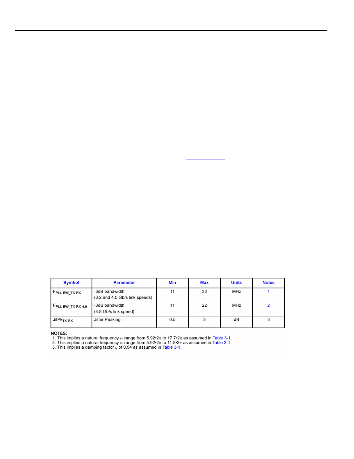
2.1 Common Specifications between Transmitter and Receiver
The TX and RX PLLs shall obey the bandwidth and jitter peaking specifications in the following table for
continuous transmission operation.
Table 1: PLL Specification for TX and RX
Fully Buffered DIMM (FB-DIMM) 1
Page 6

Methods of Implementation
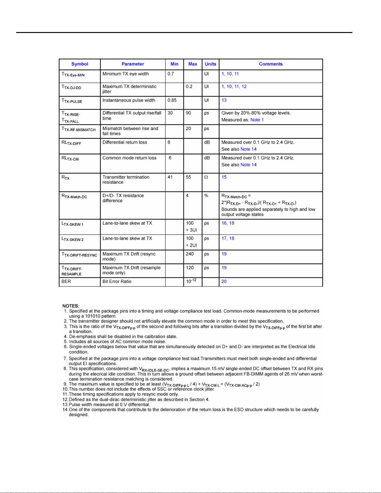
2.2 Differential Transmitter (TX) Output Specifications
See the Draft Specification for additional notes and a test definition.
Table 2: Summary of Differential Transmitter Outp ut Specifications (Sheet 1 of 2)
2 Fully Buffered DIMM (FB-DIMM)
Page 7
Methods of Implementation
Table 2: Summary of Differential Transmitter Outp ut Specifications (Sheet 2 of 2)
Fully Buffered DIMM (FB-DIMM) 3
Page 8

Methods of Implementation
2.3 Differential Transmitter (TX) Compliance Eye Diagrams
Refer Section 3.3.1 of the Draft Specification for eye diagram definition.
Figure 1: Transmitter output eye specifications, with a nd without de-emphasis
4 Fully Buffered DIMM (FB-DIMM)
Page 9
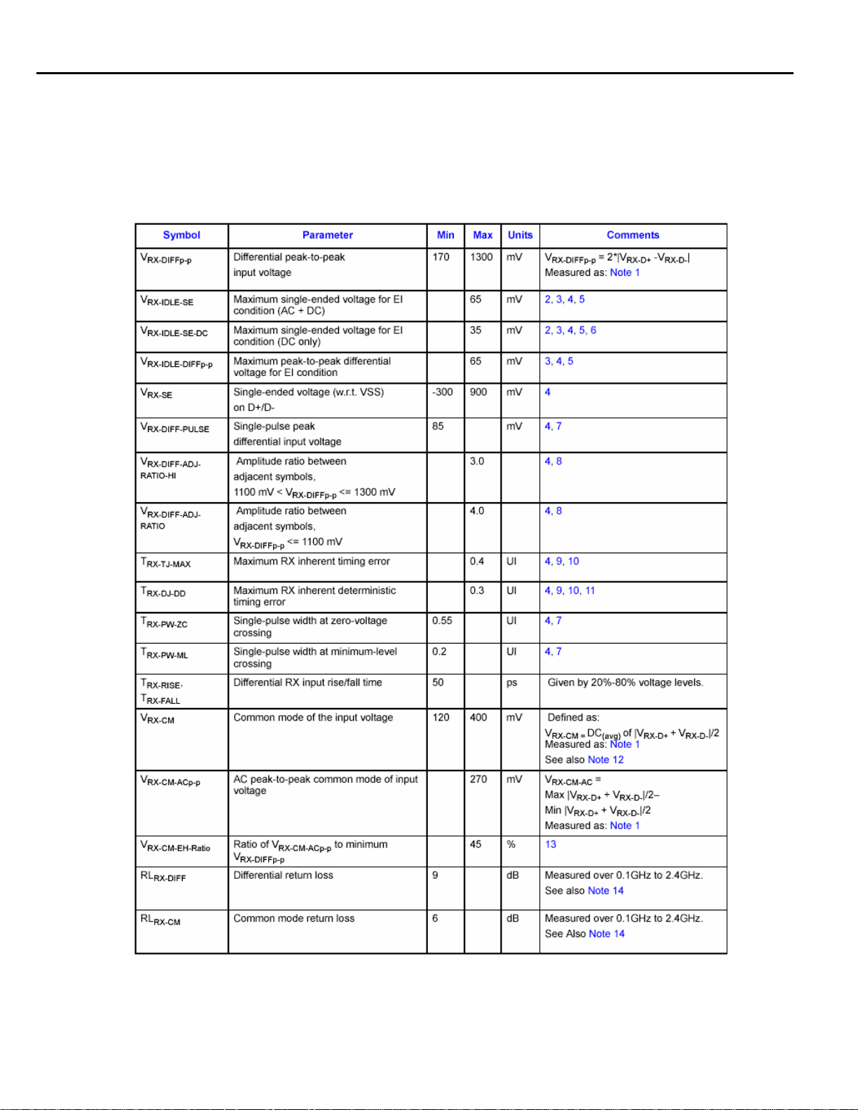
2.4 Differential Receiver (RX) Input Specifications
See the Draft Specification for additional notes and test definitions.
Table 3: Summary of Differential Receiver Input Specification (Sheet 1 of 2)
Methods of Implementation
Fully Buffered DIMM (FB-DIMM) 5
Page 10
Methods of Implementation
Table 3: Summary of Differential Receiver Input Specification (Sheet 2 of 2)
6 Fully Buffered DIMM (FB-DIMM)
Page 11
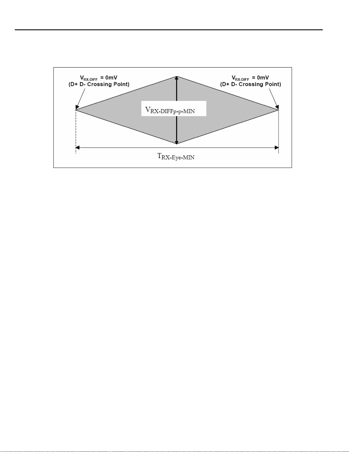
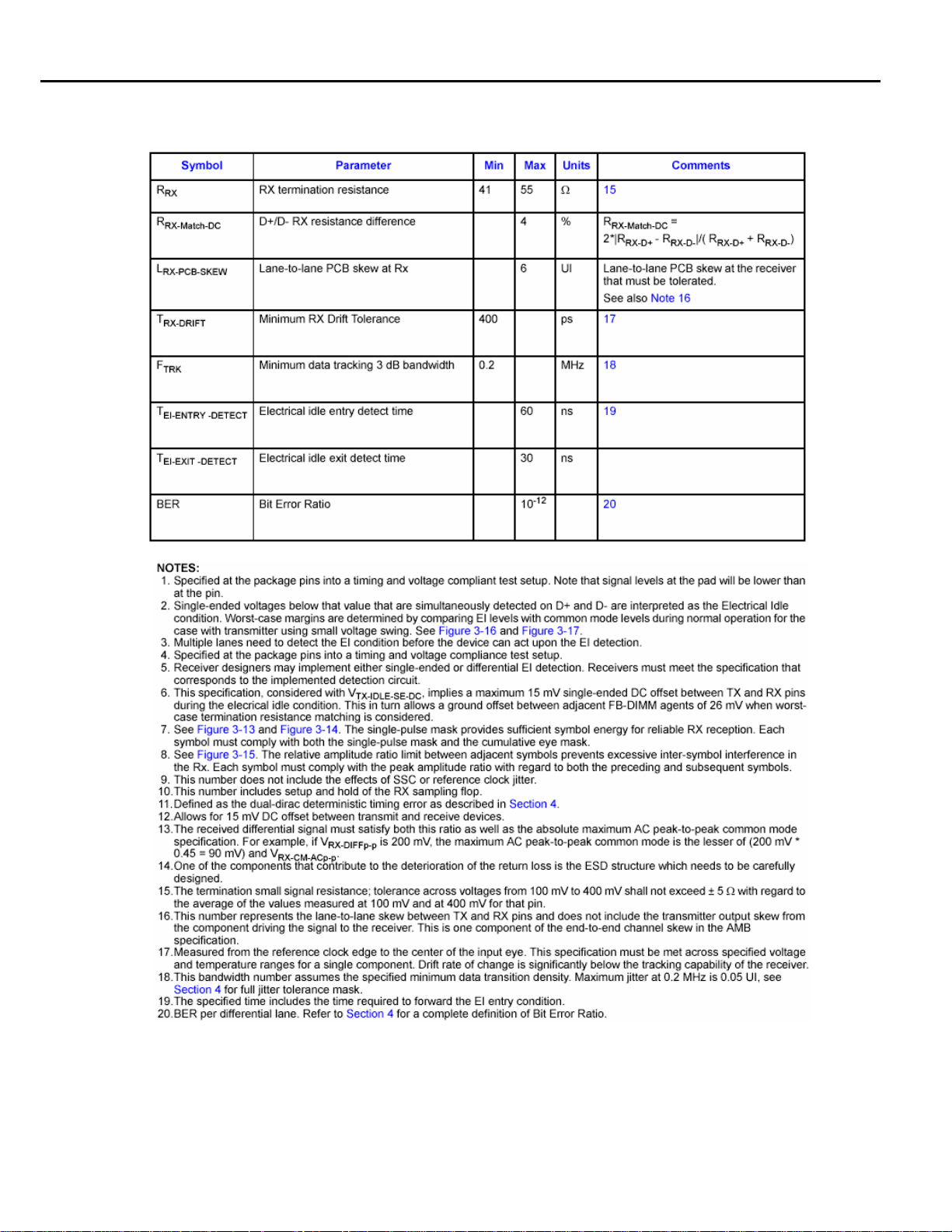
2.5 Receiver Compliance Eye Diagrams
See Section 3.4.1 of the Draft Specification for eye diagram definition.
Figure 2: Receiver input eye voltage and timing specifications
Methods of Implementation
Fully Buffered DIMM (FB-DIMM) 7
Page 12
Methods of Implementation
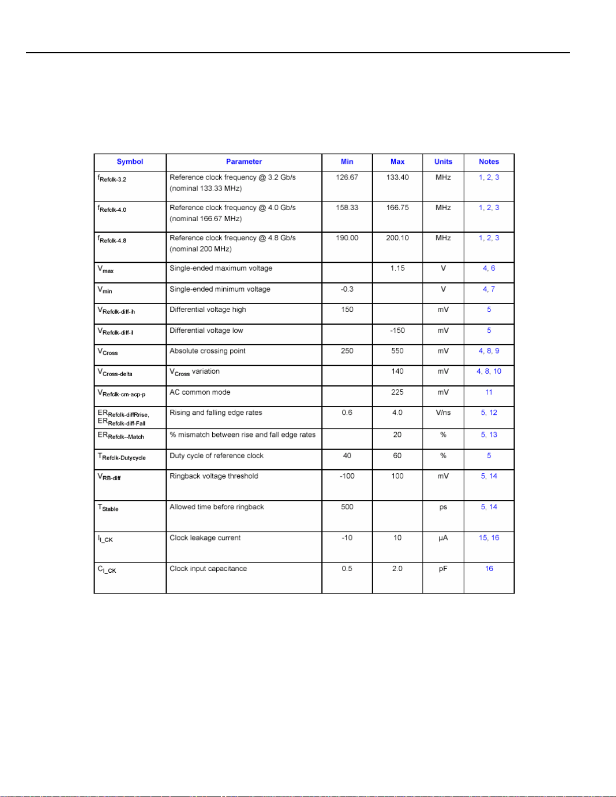
2.6 Reference Clock Specifications
See the Draft Specification for additional notes and test definitions.
Table 4: Summary of Reference Clock Input Specifications (Sheet 1of 2)
8 Fully Buffered DIMM (FB-DIMM)
Page 13
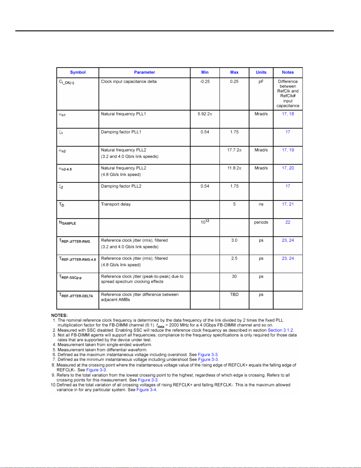
Table 4: Summary of Reference Clock Input Specifications (Sheet 2 of 2)
Methods of Implementation
Fully Buffered DIMM (FB-DIMM) 9
Page 14
Methods of Implementation
10 Fully Buffered DIMM (FB-DIMM)
Page 15

Methods of Implementation
3 Preparing to Take Measurements
3.1 Required Equipment
The following equipment is required to take measurements:
• TDS6604B/DPO70604/DSA70604 or TDS6804B/DPO70804/DSA70804 or TDS7704B or
TDS6124C or TDS6154C oscilloscope with the RT-Eye software (Opt. RTE- version 2.0) and FB-
DIMM Compliance Module (FBD) installed.
• Probes – probing configuration is MOI specific. Refer to each MOI for correct probe configuration.
• Test fixture −
1. NEX-TDSFBDP -Tektronix differential probing fixture. To access details, click the URL
http://www.busboards.com/products/scopeAccessories/tdsfbdp/index.html
2. TDSN4238B – Slot Parametric fixture is available through Tektronix.
3. New Intel DLB fixture – Contact Intel
3.2 Probing Options for Transmitter testing
The first step is to probe the link. Currently, the FB-DIMM specifications have defined the ball of the
AMB as the test point.
Note: Work is underway in the JEDEC standards committee to define CEM specifications. Tektronix
provided FBD module masks and test points are as per JEDEC standards. We also have added new masks
and new test points to be used with TDSN4238B and Intel’s DLB fixture (based on Intel’s FBD SIG test
masks). As and when the CEM specifications are defined by JEDEC, we will update our masks and test
points in our FBDIMM module.
3.2.1 SMA Connection
1. Two TCA-SMA inputs using
SMA cables (Ch1) and (Ch3)
The differential signal is created by
the RT-Eye software from the math
waveform Ch1-Ch3. The Common
mode AC measurement is also
available in this configuration from
the common mode waveform
(Ch1+Ch3)/2. This probing
technique requires breaking the
link and terminating into a
50 Ω/side termination of the
oscilloscope. While in this mode,
the FB-DIMM Serdes will transmit
the compliance test pattern (IBIST
Pattern) to maximize data
Probe Configuration A
SMA Psuedo-differential
Fully Buffered DIMM (FB-DIMM) 11
Page 16

Methods of Implementation
dependent jitter. Ch-Ch de-skew is
required as two channels are used.
This configuration does not
compensate for cable loss in the
SMA cables. The measurement
reference plane is at the input of
the TCA-SMA connectors on the
oscilloscope. Any cable loss should
be measured and entered into the
vertical attenuation menu for
accurate measurements at the SMA
Cable attachment point.
2. One P7380SMA differential
active probe (Ch1). (Only useful
for 3.2 Gb/s data rate)
The differential signal is measured
across the termination resistors
inside the P7380SMA probe. This
probing technique requires
breaking the link. While in this
mode, the FB-DIMM Serdes will
transmit the compliance test
pattern to maximize data
dependent jitter. Matched cables
are provided with the P7380 probe
to avoid introducing de-skew into
the system. Only one channel of
the oscilloscope is used. The
P7380SMA provides a calibrated
system at the Test Fixture
attachment point, eliminating the
need of compensating for cable
loss associated with the probe
configuration A.
Probe Configuration B
SMA Input Differential Probe
12 Fully Buffered DIMM (FB-DIMM)
Page 17

3.2.2 AMB Ball connection
3. Two active probes (Ch1) and
(Ch3)
The differential signal is
created by the RT-Eye
software from the math
waveform Ch1-Ch3. The
Common mode AC
measurement is also available
in this configuration from the
common mode waveform
(Ch1+Ch3)/2. This probing
technique can be used for
either a live link that is
transmitting data, or a link that
is terminated into a “dummy
load.” In both the cases, the
single-ended signals should be
probed as close as possible to
the termination resistors on
both sides with the shortest
ground connection possible.
Ch-Ch de-skew is required
because two channels are used.
4. One P7380 (3.2 Gb/s data
rate only)/P7313 Differential
probe (Ch1)
The differential signal is
measured directly across the
termination resistors. This
probing technique can be used
for either a live link that is
transmitting data, or a link
terminated into a “dummy
load.” In both cases, the
signals should be probed as
close as possible to the
termination resistors. De-skew
is not necessary as a single
channel is used.
Methods of Implementation
Probe Configuration C
Two Single-ended Active Probes
Probe Configuration D
One Differential Active Probe
Fully Buffered DIMM (FB-DIMM) 13
Page 18
Methods of Implementation
3.3 Initial Oscilloscope Setup
After connecting the Device Under Test (DUT), follow the proper probing configuration for the test. Click
the DEFAULT setup button and the AUTOSET to display the serial data bit stream.
3.4 Running the RT-Eye Software
1. Go to File> Run Application> RT-Eye Serial Compliance and Analysis. For B and C series
oscilloscopes, select App>RT-Eye …. Please refer to the OLH.
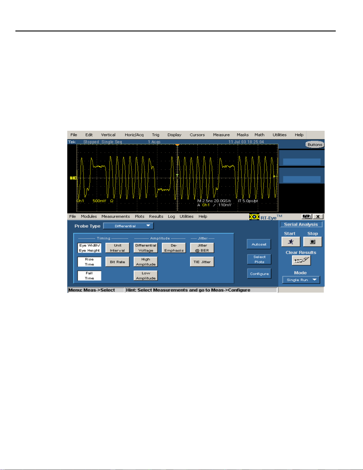
Figure 3: Default menu of the RT-Eye software
Figure 3 shows the oscilloscope display. The default mode of the software is the Serial Analysis module
(Opt. RTE-Version 2.0). This software is intended for generalized Serial Data analysis on 8B/10B encoded
copper links.
14 Fully Buffered DIMM (FB-DIMM)
Page 19
Methods of Implementation
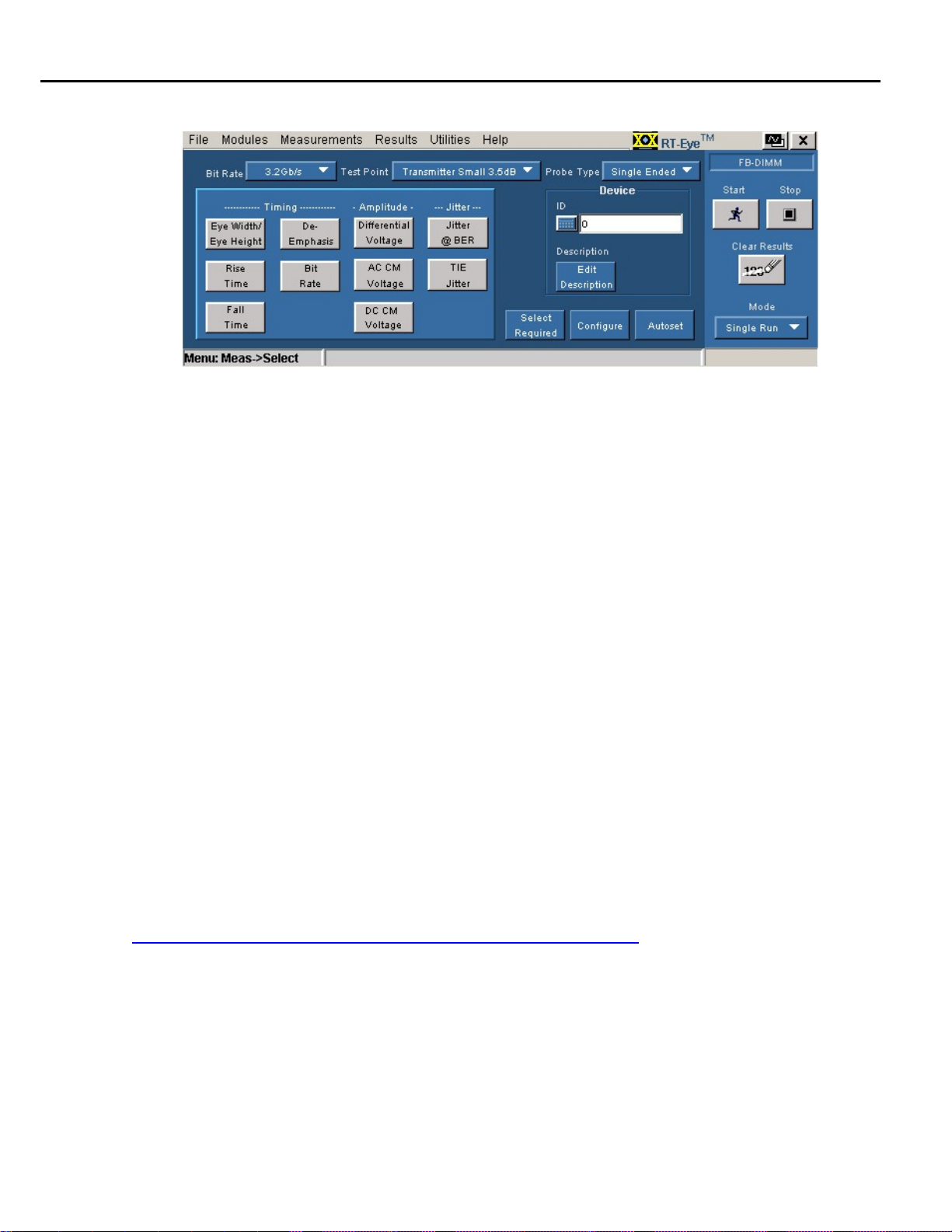
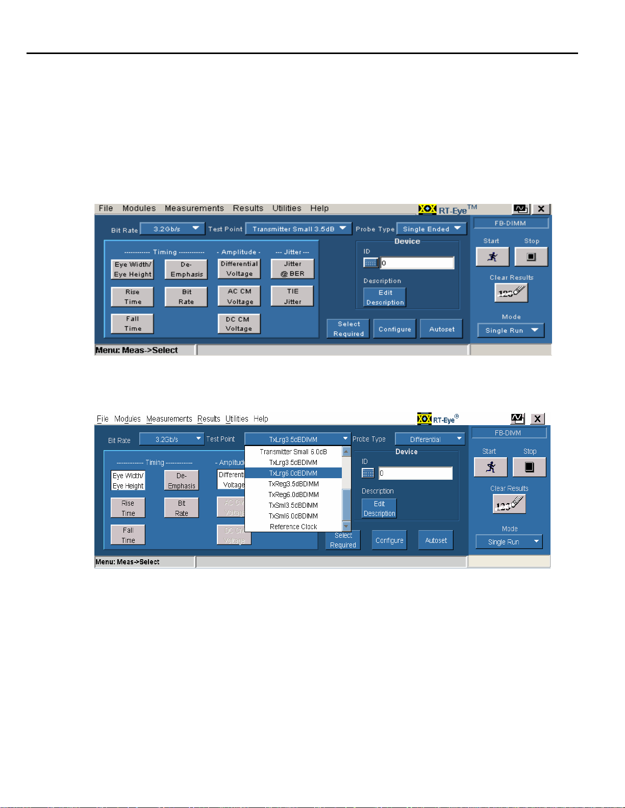
2. Select the FB-DIMM Compliance Module from the Modules pull-down list.
Figure 4: Choosing FB-DIMM Compliance Module
Note: If FB-DIMM does not appear in the list, the FB-DIMM Compliance Module (Opt. FBD) has not
been installed.
The rest of this MOI document details use of the FB-DIMM Compliance Module to perform electrical
compliance measurements.
For additional information about the FB-DIMM Compliance Module, refer to the online help, which is
available in the Help Menu for the RT-Eye software.
3.5 Clock Recovery
Second-order PLL is used. Refer to section 2.X of Common Specifications between TX and RX in the
Draft Specifications. Also refer to Table 1 of this MOI. (Serial analysis has several CDRs. You can
configure the CDR in the SA module to be exactly the same as that in FB-DIMM.)
4 FB-DIMM Receiver (RX) Compliance Testing
This section provides the Methods of Implementation (MOIs) for Receiver tests using a Tektronix real-time
oscilloscope, probes, the RT-Eye compliance software solution (version 2.0), and with the Tektronix test
fixture - NEX-TDSFBDP / TDSN4238B Slot parametric test fixture/Intel’s new DLB fixture
To order FBD scope probe kit, click
http://www.busboards.com/products/scopeAccessories/tdsfbdp/index.html
The TDSN4238B is available with Tektronix and the Intel’s new DLB fixture is available with Intel.
Fully Buffered DIMM (FB-DIMM) 15
Page 20
Methods of Implementation
4.1 Probing the Link for RX Compliance
Use probing configuration (B or D) to probe the link differentially at a point close to the pins of the
receiver device.
This method (using the Tektronix NEX-TDSFBDP FBD scope probe kit and P7313 probes) of probing at
the ball of the RX AMB:
• Is the only direct method of testing the eye opening at the receiver.
• Includes all segments of the transmission channel: TX board loss, Connector Loss (both TX and RX
side), and RX board loss.
• Both Common Mode and Differential Mode measurements can be made directly. This method
indirectly assures Slot Connector Compliance if a compliant standard blank DIMM Module is used as
the test vehicle.
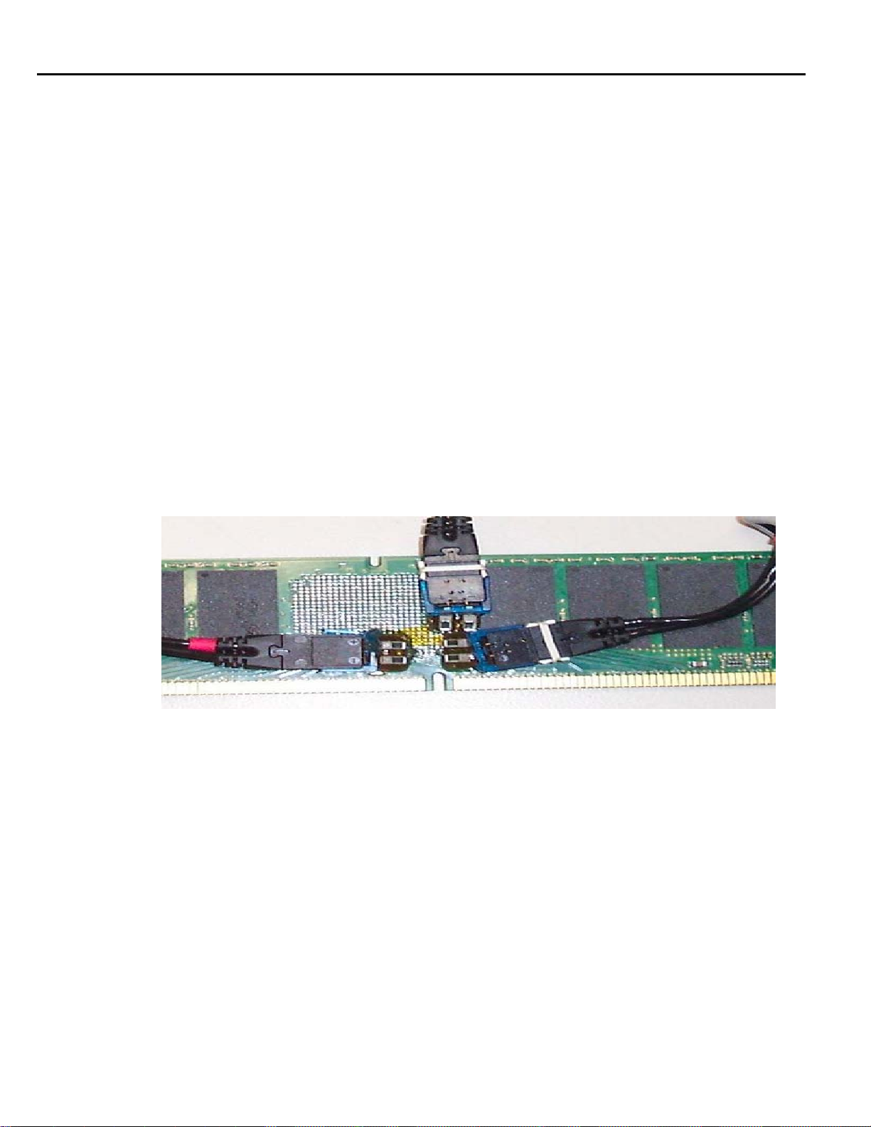
• The NEX-TDSFBDP test fixtures provide the flexibility to perform Differential and Common Mode
measurements. This test fixture consists of four blank DIMMs with ten probe tip clip connectors and
termination resistors. The user can solder up to three probe tip clip connectors to the relevant South
Bound Receiver lanes on one blank DIMM and test a maximum of three FB-DIMM South Bound
lines. The user can also configure the NEX-TDSFBDP test fixture to test the remaining seven South
Bound lanes or Reference Clock.
Figure 5: NEX-TDSFBDP test fixture
Alternatively, use probing configuration A or C using Ch1 and Ch3 inputs of an oscilloscope (using either
TDSN4238B/Intel’s DLB fixture) that has 40 GS/s sample rate available on two channels (only
TDS6124C and TDS6154C series).
4.2 Running a Complete RX Compliance Test
The MOIs for each RX test are documented in the following sections. All RX measurements can be
selected and run simultaneously with the same acquisition. To perform a compliance test of all receiver
measurements:
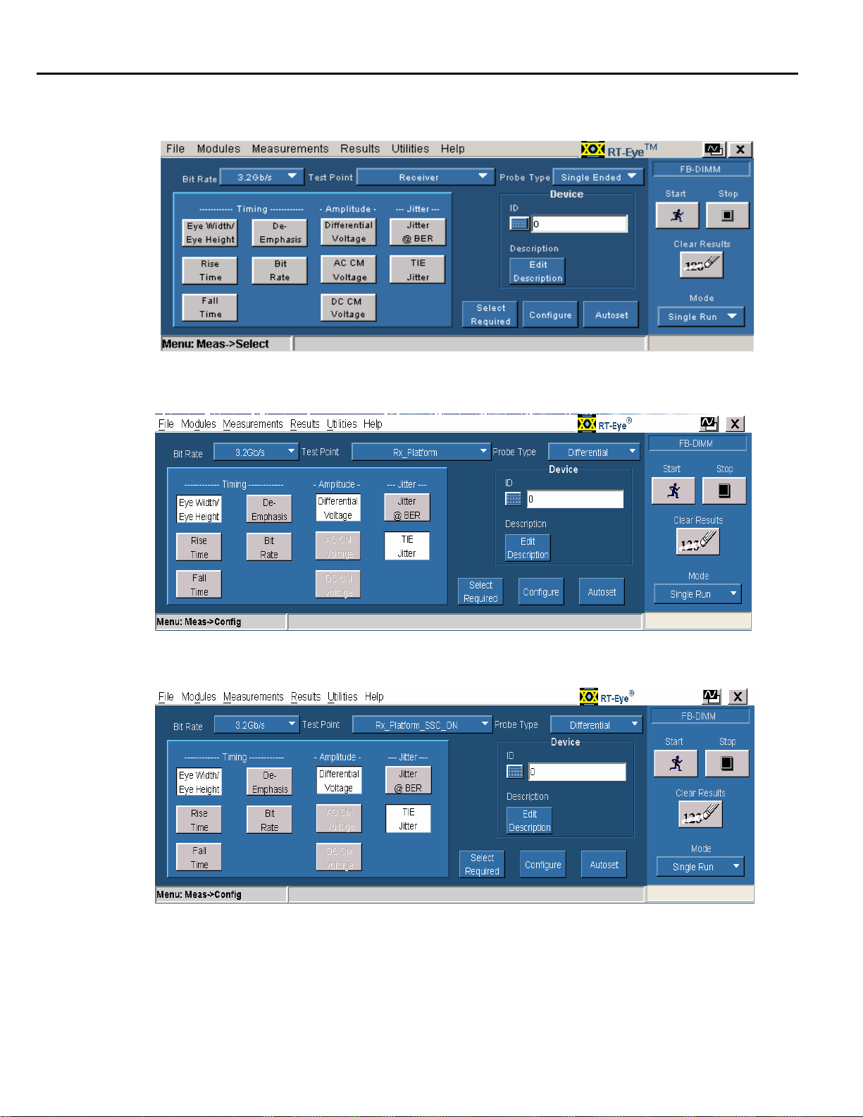
1. In the FBDIMM module, set the Bit Rate to 3.2 Gb/s, 4.0 Gb/s or 4.8 Gb/s.
2. Select Receiver or Receiver Platform (SSC on/off) from the Test Point pull-down list.
Note: The Receiver Platform (SSC on/off) selection is not available for the 4.8 Gb data rate.
16 Fully Buffered DIMM (FB-DIMM)
Page 21
Methods of Implementation
3. When you select Receiver Platform test point, the masks and limits are based on SIG Test 2.2 version
and not as per FBDIMM standards.
Figure 6a: Measurements select menu setup for Receiver test point as per FBDIMM spec
Figure 6b: Measurements select menu setup for Receiver Platform test point with SSC off when tested using the
TDSN4238B/Intel’s DLB fixture
Figure 6c: Measurements select menu setup for Receiver Platform test point with SSC on when tested using the
TDSN4238B/Intel’s DLB fixture
Fully Buffered DIMM (FB-DIMM) 17
Page 22

Methods of Implementation
4. Select Differential or Single-Ended as the Probe Type depending on your probe configuration.
5. Click Select Required to ensure that tests which have limits in FBDIMM spec or SIG Test 2.2 are
selected.
Table 5: Measurement Select/Result Cross Reference (Receiver Test Points)
Parameter
Differential peak-peak
input Voltage
Maximum RX Inherent
timing error
Maximum RX Inherent
deterministic timing error
Symbol(s)
Measurement > Select
VRX-DIFFp-p Differential voltage Diff peak Volt (max)
TRX-TJ-MAX
TRX-DJ-DD Jitter@BER Jitter Determ (Dj) max
Jitter@BER
Selection in
Menu
Results in
Measurement Results
Summary
Jitter Total (Tj) max
Differential Rx input
Rise/Fall Time
Common Mode of Input
Voltage
AC peak to peak
common Mode of input
Voltage
TRX-RISE,
TRX-FALL
VRX-CM
VRX-CM-ACp-p
Rise Time
Fall Time
DC CM Voltage
AC CM Voltage
Rise Time (min)
Fall Time (min)
CM Volt (max)
AC CM Volt(max)
6. Click Configure to access the Configuration menus and to set up Signal Source.
7. Click Autoset to auto set signal and reference levels.
8. Click Start and choose between single run or continue run.
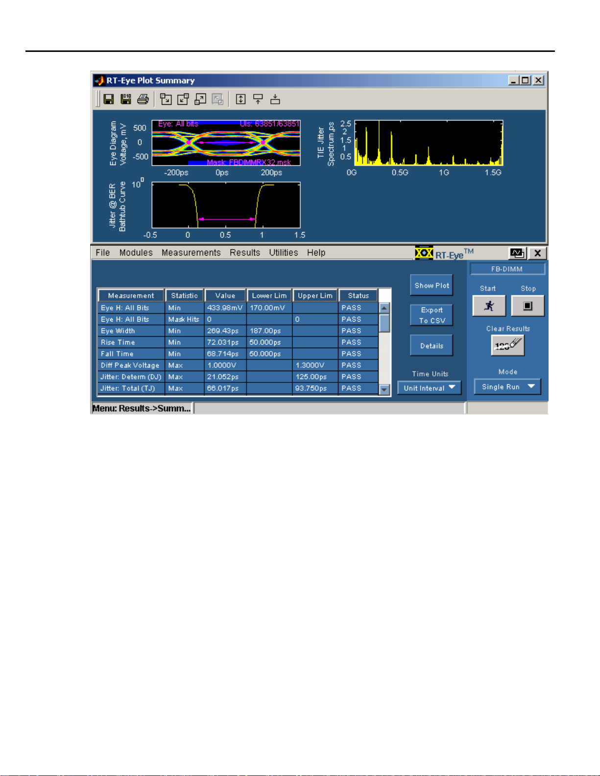
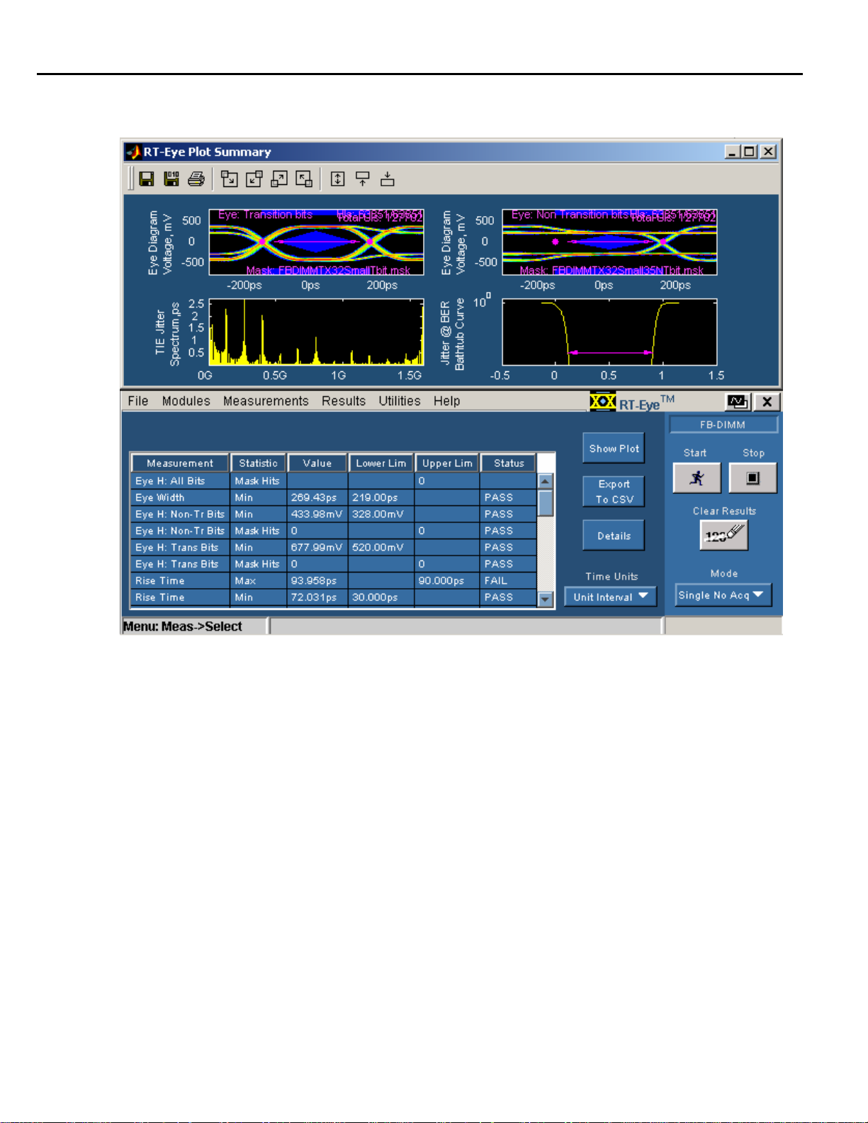
Figure 7a shows the result of a Receiver Compliance test on a signal that passes all receiver tests as per
FBDIMM specs. Note: A combined eye is rendered as per FBDIMM specs.
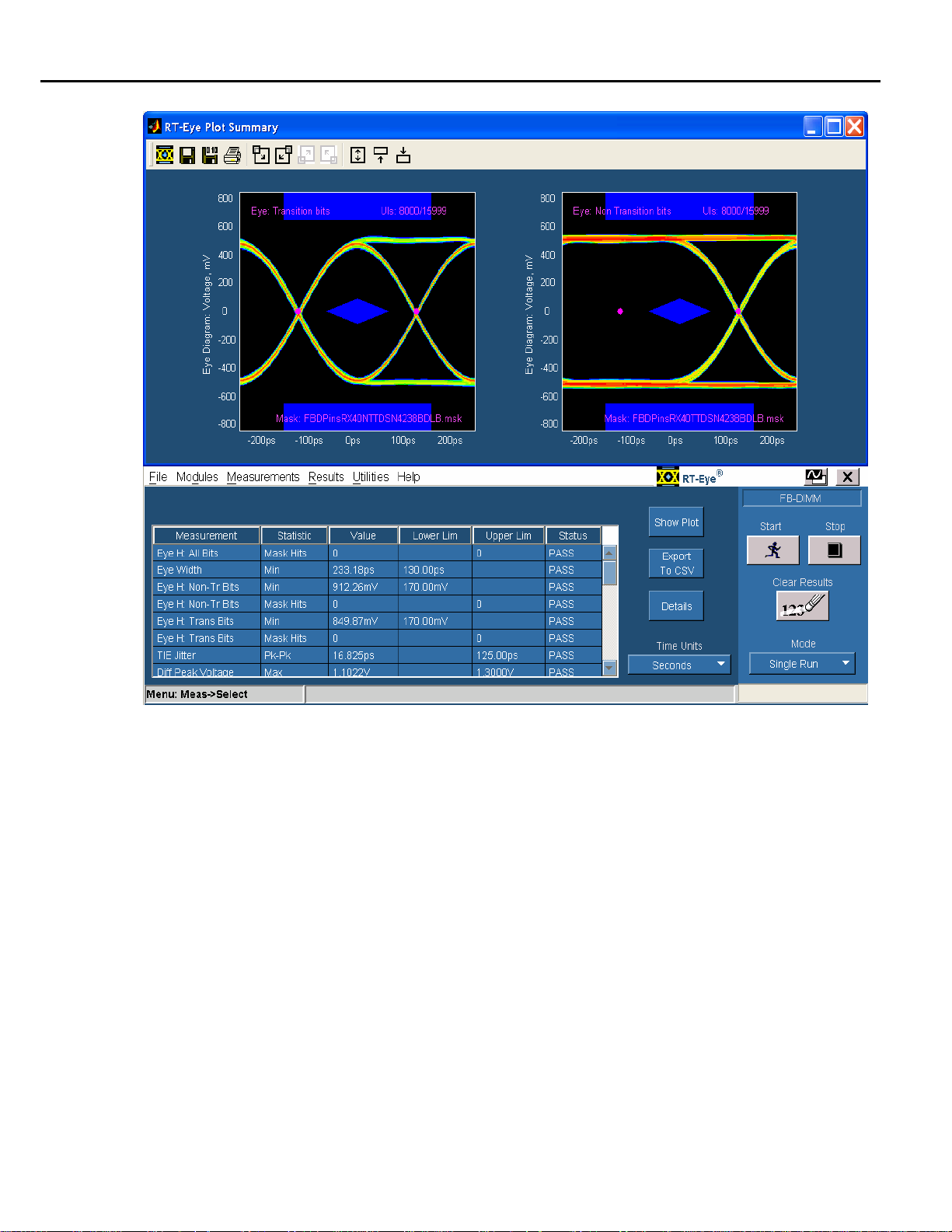
Figure 7b shows the result of a Receiver Compliance test ( SSC On/Off) on a signal that passes all receiver
tests when tested using the TDSN4238B/Intel’s DLB fixture. Note: A transition eye and Non-Transition
eye are rendered as per SIG Test 2.2.
18 Fully Buffered DIMM (FB-DIMM)
Page 23
Methods of Implementation
Figure 7a: Result of completed receiver compliance test as per FBDIMM spec
Fully Buffered DIMM (FB-DIMM) 19
Page 24
Methods of Implementation
Figure 7b: Result of completed receiver platform compliance test (SSC On/Off) when tested using TDSN4238B/Intel’s DLB
fixture
4.2.1 RX Differential Pk-Pk Input Voltage MOI
Test Definition Notes from the draft FBDIMM Specification:
-
|2
−∗=
VVV
- Specified at the measurement point and measured over the entire data. The test load in Figure 1-1 (Draft
Specification) should be used as the RX device while taking measurements. Also refer to the receiver
compliance eye diagram shown in Figure 3-12 (Draft Specification).
V
pDIFFpRX
−−
(Differential Input Pk-Pk Voltage) is defined in Table 3-4 (Draft Specification). Differential
Pk-Pk Voltage characteristics are: Maximum = 1.3 V and Minimum = 0.170 V. This measurement is
solved by two measurements: Differential Peak Voltage and Eye Height measurement.
20 Fully Buffered DIMM (FB-DIMM)
|
−−+−−−
DRXDRXpDIFFpRX
Page 25

Methods of Implementation
Test Procedure:
Follow the procedure in Section 5.3.1 (of this MOI), ensuring that Differential Voltage is selected in the
Measurements> Select menu.
PASS Condition:
V
pDIFFpRX
−−
< 1.3 V and 170 mV < Eye Height
Measurement Algorithm:
Refer to section 5.3.1 of this MOI document for Differential Voltage measurement and Eye Height
measurement algorithms.
Note: For receiver testing, Eye Height is measured on all UIs. There is no separate Eye Height for
Transition bits measurement and Non-Transition bits measurement
4.2.2 Minimum RX Eye Width MOI
Test Definition Notes from the draft FBDIMM Specification:
- The maximum interconnect media and transmitter jitter that can be tolerated by the receiver can be
derived as
from it to get T_RX-EYE.
- Specified at the measurement point and measured over the entire data. The test load in Figure 1-1 (Draft
Specification) should be used as the RX device while taking measurements. Also refer to the receiver
compliance eye diagram shown in Figure 3-12 (Draft Specification).
- A TJ = 0.4 UI provides for a total sum of deterministic and random jitter budget for the transmitter and
interconnect.
UITT
6.1=−=
EYERXJITTERMAXRX
−−−
. T_RX-TJ_MAX in Table 3-4 is 0.4 UI. You can derive
Test Procedure:
Follow the procedure in Section 4.3 (Draft Specification), ensuring that Eye Width/Eye Height is
selected in the Measurements> Select menu.
Measurement Algorithm:
Refer to section 3.4.1 and 4.8 of the Draft Specification for Eye Width measurement algorithm.
Note: When you select the Receiver platform (SSC on/off) test point, the minimum Eye width limit is
based on the SIG Test 2.2 version and is different from the FBDIMM specification.
Fully Buffered DIMM (FB-DIMM) 21
Page 26

Methods of Implementation
4.2.3 RX AC Common Mode Input Voltage MOI
Test Definition Notes from the draft FBDIMM Specification:
=−−
++
ACCMVRX
- Specified at the measurement point and measured over entire data. The test load in Figure 1-1 (Draft
Specification) should be used as the RX device when taking measurements. Also refer to the receiver
compliance eye diagram shown in Figure 3-12 (Draft Specification). (AC Peak Common
Mode Input Voltage) is defined in Table 3-4 (Draft Specification).
Limits:
Maximum = 270 mV and the pass condition is 270 mV >
Test Procedure:
Follow the procedure in Section 4.3 (Draft Specification), ensuring that AC CM Voltage is selected in
the Measurements> Select menu.
Note: AC CM voltage is available only when you select Single-ended probe type.
Measurement Algorithms:
This measurement is made over the entire data defined in Section 3.4 (Draft Specification).
-D-VRXD-X −−++−
−
DVRXDVRXMinVRMax
22
ACpCMRXV−−
ACpCMRXV−−
AC CM Pk Voltage Measurement:
The AC Common Mode Pk Voltage measurement returns the peak-to-peak value of common mode
(Peak-to-peak value is not affected by DC).
4.2.4 RX DC Common Mode Input Voltage MOI
Test Definition Notes from the Specification:
VR
=−
)(
ofavgDCCMVRX
++
2
- Specified at the package pins into a timing and voltage compliant test load. Note that the signal levels at
the pad will be lower than at the pin.
Limits:
Maximum = 400mV and Minimum = 120mV
-D-VRXD-X
22 Fully Buffered DIMM (FB-DIMM)
Page 27

Test Procedure:
Methods of Implementation
Follow the procedure in Section 4.3 (Draft Specification), ensuring that DC CM Voltage
the Measurements> Select menu (Note: DC CM Voltage is only available when you select Single-
Ended probe type.)
Measurement Algorithms:
This measurement is made over the entire data defined in Section 3.4 (Draft Specification).
The DC Common Mode measurement:
The DC Common Mode measurement returns the DC Average of the Common Mode Voltage waveform.
4.2.5 RX Waveform Eye Diagram Mask Test MOI
Test Definition Notes from the Specification:
- The RX eye diagram in Figure 3-12 (Draft Specification) is specified using the passive compliance/test
measurement load (see Figure 1-1, Draft Specification) in place of any real FB-DIMM RX component.
Note: In general, the minimum Receiver eye diagram measured with the compliance/test measurement
load (see Figure 1-1, Draft Specification) will be larger than the minimum Receiver eye diagram
measured over a range of systems at the input receiver of any real FB-DIMM component. The degraded
eye diagram at the input receiver is due to traces internal to the package as well as silicon parasitic
characteristics, which cause the real FB-DIMM component to vary in impedance from the
compliance/test measurement load. The input receiver eye diagram is implementation specific and is not
specified. The RX component designer should provide additional margin to adequately compensate for
the degraded minimum receiver eye diagram (shown in Figure 3-12, Draft Specification) expected at the
input receiver based on some adequate combination of system simulations and the return loss measured
looking into the RX package and silicon.
is selected in
- The RX Eye diagram must be aligned in time using the jitter median to locate the center of the eye
diagram.
- The Eye diagram must be valid for the entire data.
Test Procedure:
Follow the procedure in Section 4.3 (Draft Specification), ensuring that Eye Width /Eye Height
selected in the Measurements> Select menu.
Fully Buffered DIMM (FB-DIMM) 23
is
Page 28

Methods of Implementation
Measurement Algorithm:
This measurement is made over the entire data defined in Section 3.4 (Draft Specification).
The acquisition points are compared to the mask geometry (defined in Figure 4.24, Draft Specification)
and mask collisions are reported as Mask Hits in the Measurement Results area.
If Mask Hits > 0, then a failure is indicated in the Measurement Results table.
Note: When you select Receiver Platform (SSC on/Off) test point, the Eye mask coordinates are as per
SIG Test 2.2 version and are different from the FBDIMM Receiver mask coordinates.
4.2.6 RX Input Rise/Fall Time test MOI
Test Definition Notes from the Specification:
- Specified at the measurement point into a timing and voltage compliance test load as shown in Figure
1.1 (Draft Specification) and measured over the entire data. Also refer to the Receiver compliance (Draft
Specification).
- Measured between 20-80% at Receiver pins into a test load as shown in Figure 1.1 (Draft Specification)
for both and
V
,
RISERXT−
V
+−DRX
(D+/D- RX output Rise/Fall Time) is defined in Table 3-3 (Draft Specification).
FALLRXT−
−−DRX
Limits (specified only at Receiver pins compliance point):
Minimum = 50ps.
Test Procedure:
Follow the procedure in Section 4.3 (Draft Specification), ensuring that Rise Time and Fall Time are
selected in the Measurements> Select menu.
Measurement Algorithm:
This measurement is made over the entire duration of RX test pattern defined in Section 4 (Draft
Specification).
Rise/Fall time is limited to rising or falling edges of consecutive transitions for transmitter
measurements. (Even for single-ended, the differential waveform is computed and then the rise/fall
measurement performed.)
Note: Change the following descriptions to differential waveform only.
24 Fully Buffered DIMM (FB-DIMM)
Page 29

Methods of Implementation
−
Rise Time: The Rise Time measurement is the time difference between when the V
is crossed and the V
reference level is crossed on the rising edge of the waveform.
REF-LO
−=
)()()( jtitnt
LOHIRISE ++
Where:
t is a Rise Time measurement
RISE
t
is a set of only for rising edges
+HI
t is a set of only for rising edges
+LO
i and j are indexes for nearest adjacent pairs of and
t
HI
t
LO
t
t
+LO
+HI
n is a the index of rising edges in the waveform
Fall Time: The Fall Time measurement is the time difference between when the V
crossed and the V
=
reference level is crossed on the falling edge of the waveform.
REF-LO
)()()( jtitnt
HILOFALL −−
reference level
REF-HI
reference level is
REF-HI
Where:
t
is a Fall Time measurement
FALL
t
is set of t
HI–
t
is set of t
LO–
only for falling edge
HI
LO
i and j are indexes for nearest adjacent pairs of t
n-is the index to falling edges in the waveform
4.2.7 RX Tj Test MOI
Test Definition Notes from the Specification:
Trx-Tj-Max Maximum receiver inherent timing error (Jitter)
Specified at the package pins into a timing and voltage compliance test load.
This value does not include the effects of SSC or ref clk jitter.
This includes the setup and hold of receiving sampling clock.
only for falling edge
LO–
and t
HI–
.
Limits:
Maximum = 0.4 UI
Fully Buffered DIMM (FB-DIMM) 25
Page 30

Methods of Implementation
Test Procedure:
Follow the procedure in Section 4.3 (Draft Specification), ensuring that Jitter@BER is selected in the
Measurements> Select menu.
Measurement Algorithm:
Total jitter is usually comprised of both random and deterministic components. In general, the DJ
component has its own PDF (Probability Distribution function), and the combined total jitter PDF is a
convolution of the DJ and RJ PDF’s. The Rx-Tj is estimated by equivalently deriving the CDF
(Cumulative Distribution Function) at measured points and extrapolating to a BER < 10
device exceeding the TJ specification is identified with a 99.7% confidence interval.
Note: When you select Receiver Platform (SSC on/off) test point, TIE pk-pk jitter value is calculated
based on the SIG Test 2.2 version and is different from the FBDIMM Receiver specifications for Jitter.
-9
, such that a
26 Fully Buffered DIMM (FB-DIMM)
Page 31

4.2.8 RX Dj Test MOI (Using Dual-Dirac Method)
Test Definition Notes from the Specification:
-This is the Maximum inherent deterministic timing error (Jitter) specified at the package pins into a
timing and voltage compliance test load.
-This value does not include the effects of SSC or ref clk jitter.
-This includes the setup and hold of receiving sampling clock.
-Defined as the Dual-Dirac timing error.
Limits:
Maximum = 0.3 UI
Test Procedure:
Follow the procedure in Section 4.3 (Draft Specification), ensuring that Jitter@BER is selected in the
Measurements> Select menu.
Measurement Algorithm:
Methods of Implementation
The DJ PDF is defined as a pair of Dirac delta functions (Dual-Dirac). The Dual-Dirac model is assumed
for system. The Dual-Dirac description is merely the linearization of the CDF (Cumulative Distribution
Function) at a particular BER. Since the CDF has two sides, this linearization is performed twice, and the
result is then combined. The Rx-Dj is estimated by equivalently deriving the CDF at measured points and
extrapolating to a BER < 10
-9
, such that a device exceeding the DJ specification is identified with a
99.7% confidence interval.
Fully Buffered DIMM (FB-DIMM) 27
Page 32
Methods of Implementation
5 FB-DIMM Transmitter (TX) Compliance Testing
This section provides the Methods of Implementation (MOIs) for Transmitter tests using a Tektronix realtime oscilloscope, probes, and the RT-Eye compliance software with FB-DIMM (FBD) Module.
5.1 Probing the Link for TX Compliance
Use probing configuration (B or D) to probe the link differentially at a point close to the pins of the
receiver device.
Alternatively, use probing configuration (A or C) using the Ch1 and Ch3 inputs of an oscilloscope that has
a 40 GS/s sample rate available on two channels along with an SMA break-out fixture or
TDSN4238B/Intel’s DLB test fixture (TDS6124C and TDS6154C Series).
Since probing at the ball of the TX AMB is not practical, you can use an SMA break-out fixture or a
JEDEC approved parametric fixture (TDSN4238B ) or the new Intel DLB test fixture to test the TX points.
However use care about the following when you use an SMA break-out fixture or a JEDEC approved
parametric fixture:
• Compensation of all the losses: a.) Transmission channel; TX board loss, b.) Connector Loss (both TX
and RX side), and c.) RX board losses are taken into consideration.
• Pseudo-differential measurements should be performed carefully and channel deskew plays an
important role.
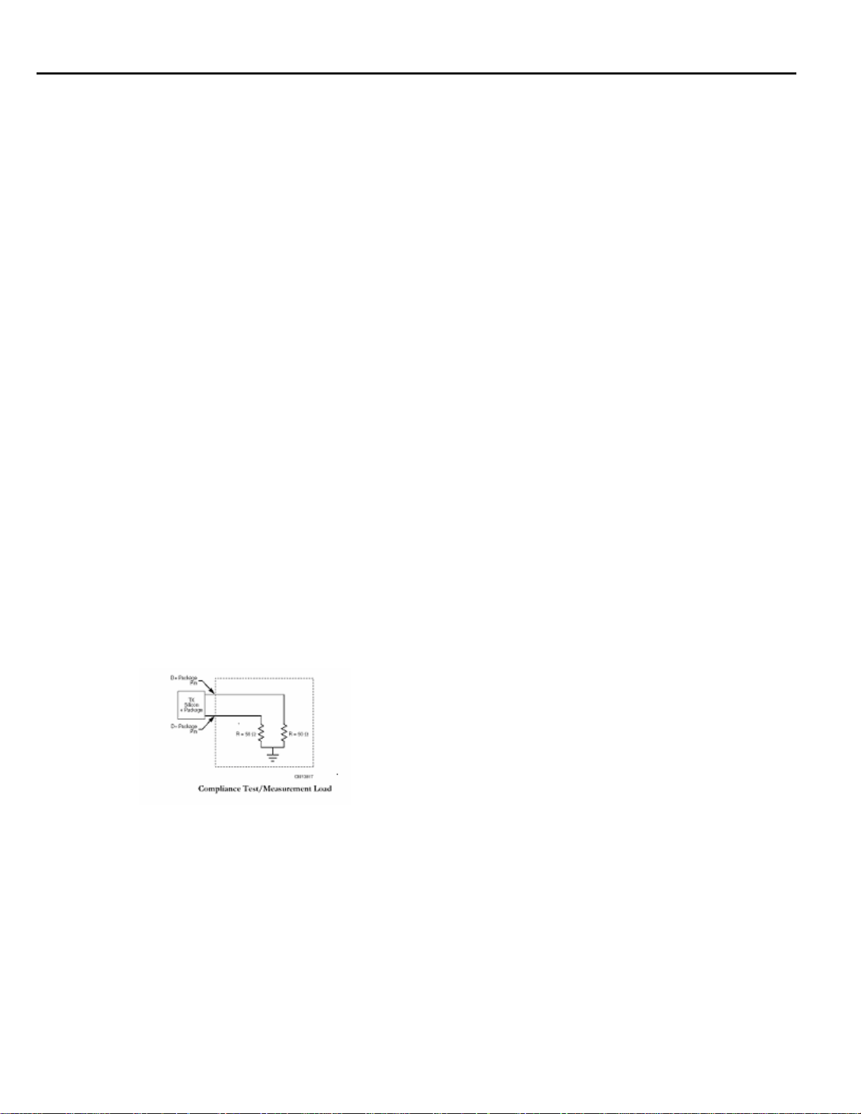
5.1.1 TX Compliance Test Load
The compliance test load for Transmitter compliance is shown in Figure 8.
Figure 8: Transmitter Compliance Test Load
28 Fully Buffered DIMM (FB-DIMM)
Page 33

Methods of Implementation
5.2 Running a TX Compliance Test
The only test point defined in the FB-DIMM specifications, for the TX Compliance Test is the TX pins on
the ball of the AMB. You can use the SMA break-out test fixture or the JEDEC test fixture (measures at
the connector and not at the ball of the AMB) if it is available. Care should be taken to ensure that the test
fixture does not add losses to the FB-DIMM signals. The test point that will be defined by the transmitter
test in the FB-DIMM Compliance Module is defined at installation of Version 2.0 of the RT-Eye software.
Version 2.0 supports only the Transmitter Pins Compliance point. Refer to section 3.2 for more
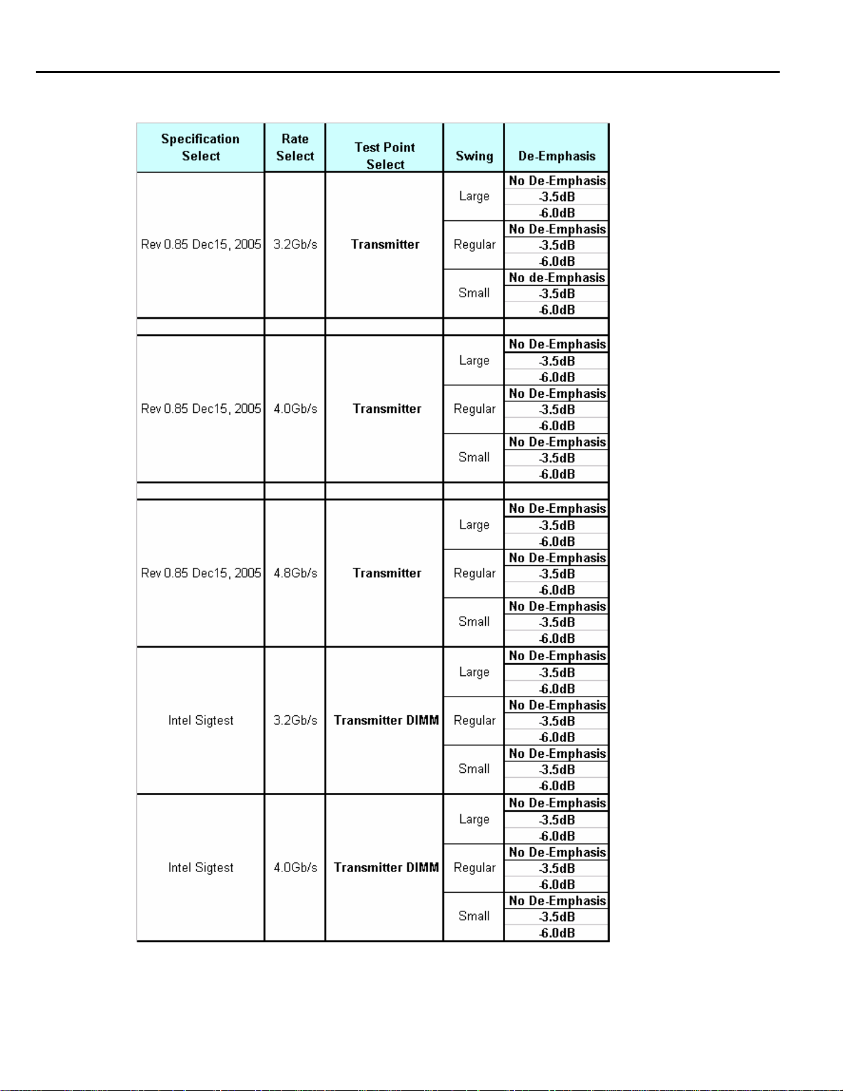
information on installing the proper test point. The transmitter data rates can be 3.2 GB/s, 4.0 Gb/s, or 4.8
Gb/s. Each of these rates can have three voltage swing settings and in each voltage swing setting you can
have three de-emphasis levels. The following table provides the details:
Fully Buffered DIMM (FB-DIMM) 29
Page 34
Methods of Implementation
Table 6: Transmitter test point details
30 Fully Buffered DIMM (FB-DIMM)
Page 35
Methods of Implementation
The MOI for each of the Transmitter tests is documented in the following sections. All Transmitter
measurements can be selected and run simultaneously with the same acquisition. To perform a compliance
test of all transmitter measurements:
1. In the Measurements> Select menu (Figure 9a), select Bit rate (3.2/4.0/4.8 Gb/s).
2. Click Transmitter (small/regular/large) or Transmitter DIMM from the Test Point pull-down list.
Note: Transmitter DIMM selection is not available for 4.8 Gb data rate.
Figure 9a: Measurements select menu setup for Transmitter small/regular/large 3.5db or 6dB de-emphasis levels as per
FBDIMM specifications
Figure 9b: Measurements select menu setup for Transmitter DIMM small/regular/large 3.5db or 6dB de-emphasis levels as
per FBDIMM specifications
3. Select Single-Ended (probe configurations A & C defined in Section 3) or Differential (Probe
configurations B & D defined in Section 3) as the Probe Type depending on your probe configuration.
4. Click Configure to access the Configuration menus and set up the Signal Source. Click Select to
return to the Measurements> Select menu.
Fully Buffered DIMM (FB-DIMM) 31
Page 36

Methods of Implementation
5. Click the desired measurements or click Select Required. Note: When you select Transmitter DIMM
Test Point and when “select required” is clicked only Eye width/Eye height, Differential voltage and
TIE Jitter tests are selected.
Table 7: Measurement Select/Result Cross Reference (Transmitter Test Points)
Parameter to
measure
Differential p-p TX
voltage swing
VTX-DIFFp-p_S Differential Voltage
Symbol(s)
Selection in
Measurement > Select
Menu
Results in
Measurement Results
Summary
Diff Peak Volt (Max)
De-emphasized output
voltage ratio
Max SE Voltage in EI
condition
Max SE Voltage in EI
condition DC only
Minimum TX Eye
width
Instantaneous Pulse
width
Max Tx Deterministic
jitter
Differential TX output
rise/fall Time
AC p-p common mode
output voltage
DC common mode
output voltage
VTX-DE-3.5-Ratio
VTX-DE-6.0-Ratio
VTX-IDLE-SE Not supported in RT-Eye
VTX-IDLE-SE-DC
TTX-Eye-MIN
TTX-PULSE
T
TX-DJ-DD
TTX-RISE,
TTX-FALL
VTX-CM-ACp-p L
De-Emphasis
FBDIMM module
Not supported in RT-Eye
FBDIMM module
Eye Width Eye Width (Min)
Jitter@BER Jitter determ(Dj) Max
For Gen1: TIE Jitter
For Gen2: Not Specified
Rise Time
Fall Time
AC CM Voltage
VTX-CM-ACp-p R
VTX-CM-ACp-p S
VTX-CM_L
VTX-CM_S
DC CM Voltage
De-Emphasis (Mean)
-
-
Gen1: TIE Jitter (Min) or
TIE Jitter (Max); whichever
value has the maximum
deviation from the Median.
Rise Time (Max,Min)
Fall Time (Max,Min)
AC CM Voltage (Max)
CM Voltage(Max)
6. Click Autoset to auto set signal and reference levels.
7. Click Start.
32 Fully Buffered DIMM (FB-DIMM)
Page 37
Methods of Implementation
Figure 10 shows the result of a Transmitter Compliance test on a signal that passes the transmitter tests at
TX compliance test points.
Figure 10a: Result of a completed compliance test at the transmitter pins as per FBDIMM specifications
Fully Buffered DIMM (FB-DIMM) 33
Page 38

Methods of Implementation
Figure 10b: Result of a completed compliance test on selecting transmitter DIMM test point while using the
TDSN4238B/Intel DLB fixture
5.2.1 TX Differential Pk-Pk Output Voltage MOI
Test Definition Notes from the Specification:
-
−∗=
VVV
- Specified at the measurement point into a timing and voltage compliance test load as shown in Figure 11 (Draft Specification) and measured over entire TX test pattern as specified in section 4 of the draft
specification. Also refer to the transmitter compliance eye diagram shown in Figure 3-9 (Draft
Specification).
V
pDIFFpTX
−−
(Differential Output Pk-Pk Voltage) is defined in Table 3-3 (Draft Specification).
Differential Pk-Pk Voltage characteristics are:
Maximum = 1.3 V and
||2
−−+−−−
DTXDTXpDIFFpTX
34 Fully Buffered DIMM (FB-DIMM)
Page 39

Methods of Implementation
Minimum = 0.90 V (large swing).
or
Minimum = 0.80V (medium swing).
or
Minimum = 0.520V (small swing).
This measurement is solved by two measurements - Differential Peak Voltage measurement and Eye
Height: Transition bits measurement. Select Differential Voltage and Eye Width/Eye Height, to get five
measurements: Eye Height, Eye Height: Transition bits, Eye Height: Non-Transition bits, Eye Width and
Differential Peak Voltage.
Test Procedure:
Follow the procedure in Section 4.4 (Draft Specification), ensuring that Differential Voltage and Eye
Width/Eye Height are selected in the Measurements> Select menu.
Pass Condition:
Transmitter Pins Compliance Test Point:
Large Voltage Swing:
Transition Bit: < 1.3 V and 0.900 V < Eye Height (No de-emphasis).
Non-Transition Bit: < 1.3 V and 0.567 V < Eye Height (-3.5 dB de-emphasis).
Non-Transition Bit: < 1.3 V and 0.402 V < Eye Height (-6.0 dB de-emphasis).
V
V
V
pDIFFpTX
−−
pDIFFpTX
−−
pDIFFpTX
−−
Regular Voltage Swing:
Transition Bit: < 1.3 V (Not in the table 3-3 in spec) and 0.800 V < Eye Height (No
V
pDIFFpTX
−−
de-emphasis).
Non-Transition Bit: < 1.3 V and 0.504 V < Eye Height (-3.5 dB de-emphasis).
Non-Transition Bit: < 1.3 V and 0.357 V < Eye Height (-6.0 dB de-emphasis).
V
V
pDIFFpTX
−−
pDIFFpTX
−−
Small Voltage Swing:
Transition Bit: < 1.3 V and 0.520 V < Eye Height (No de-emphasis).
Non-Transition Bit: < 1.3 V and 0.328 V < Eye Height (-3.5 dB de-emphasis).
Non-Transition Bit: < 1.3 V and 0.232 V < Eye Height (-6.0 dB de-emphasis).
V
V
V
pDIFFpTX
−−
pDIFFpTX
−−
pDIFFpTX
−−
Fully Buffered DIMM (FB-DIMM) 35
Page 40

Methods of Implementation
−
−
=
Measurement Algorithm:
These measurements are made over the entire TX test pattern defined in Section 4 (Draft Specification).
Differential Peak Voltage Measurement: The Differential Peak Voltage measurement returns two times
the larger of the Min or Max statistic of the differential voltage waveform.
Where:
i is the index of all waveform values.
v
DIFF
is the Differential voltage signal.
Eye Height Measurement:
The measured minimum vertical eye opening at the UI center as shown in the plot of the eye diagram.
There are three types of Eye Height values:
Eye Height – Transition:
=
VVV
Where:
V
V
MINTRANHIEYE
−−−
is the minimum of the high transition bit eye voltage at mid UI.
MAXTRANLOEYE
−−−
is the maximum of the low transition bit eye voltage at mid UI.
Eye Height – Non-Transition:( -3.5 dB and -6 dB)
VVV
Where:
V
V
MINNTRANHIEYE
−−−
is the minimum of the high non-transition bit eye voltage at mid UI.
MAXNTRANLOEYE
−−−
is the maximum of the low non-transition bit eye voltage at mid UI.
MAXTRANLOEYEMINTRANHIEYETRANHEIGHTEYE
−−−−−−−−
MAXNTRANLOEYEMINNTRANHIEYENTRANHEIGHTEYE
−−−−−−−−
36 Fully Buffered DIMM (FB-DIMM)
Page 41

5.2.2 TX De-Emphasized Differential Output Voltage (Ratio) MOI
Test Definition Notes from the Specification:
Methods of Implementation
- This is the ratio of of the second and following bits after a transition divided by
the of the first bit after a transition.
V
pDIFFpTX
−−
V
pDIFFpTX
−−
- Specified at the measurement point into a timing and voltage compliance test load as shown in Figure 311 (Draft Specification. Also refer to the transmitter compliance eye diagram shown in Figure 3-9 (Draft
Specification).
(De-Emphasized Differential Output Voltage (Ratio)) is defined in Table 3-3 (Draft
RATIODETXV−−
Specification).
Limits (specified only at transmitter pins compliance test point):
Maximum = -4.0 dB and Minimum = -3.0 dB, and the Pass Condition is
-3.0 dB < < -4.0 dB
RATIODETXV−−
Limits (specified only at transmitter pins compliance test point):
Maximum = -7.0 dB and Minimum = -5.0 dB, and the Pass Condition is
-5.0 dB < < -7.0 dB
RATIODETXV−−
Test Procedure:
Follow the procedure in Section 4.4 (Draft Specification), ensuring that De-Emphasis is selected in the
Measurements> Select menu.
Fully Buffered DIMM (FB-DIMM) 37
Page 42

Methods of Implementation
Measurement Algorithm:
This measurement is made over the entire data defined in Section 3.4 (Draft Specification). The DeEmphasis measurement calculates the ratio of any non-transition eye voltage (2
succeeding an edge) to its nearest preceding transition eye voltage (1
st
eye voltage following an edge). In
nd
, 3rd, etc. eye voltage
Figure 11, it is the ratio of the black voltages over the blue voltages. The results are given in dB.
Figure 11: De-emphasis measurement
⎛
⎜
=
)(
dBmDEEM
⎜
⎝
−−
NTRANHIEYE
−−
TRANHIEYE
⎞
)(
mv
⎟
⎟
)(
nv
⎠
or
⎛
⎜
=
)(
dBmDEEM
⎜
⎝
−−
NTRANLOEYE
−−
TRANLOEYE
⎞
)(
mv
⎟
⎟
)(
nv
⎠
Where:
TRANHIEYEv−−
is the high voltage at mid UI following a positive transition.
TRANLOEYEv−−
is the low voltage at mid UI following a negative transition.
NTRANHIEYEv−−
is the high voltage at mid UI following a positive transition bit.
NTRANLOEYEv−−
is the low voltage at mid UI following a negative transition bit.
m is the index for all non-transition Uis.
n is the index for the nearest transition UI preceding the UI specified by m.
38 Fully Buffered DIMM (FB-DIMM)
Page 43

5.2.3 Minimum TX Eye Width MOI
Test Definition Notes from the Specification:
(Minimum TX Eye Width) is defined in Table 3-3 (Draft Specification).
EYETXT−
Limits:
Methods of Implementation
Transmitter pins compliance test point: 0.70 UI (218.75ps) < for 3.2Gb/s rate.
Transmitter pins compliance test point: 0.70 UI (175.00ps) < for 4.0Gb/s rate.
Transmitter Pins compliance test point: 0.70 UI (154.0ps) < for 4.8 GB/s rate.
EYETXT−
EYETXT−
EYETXT−
Test Procedure:
Follow the procedure in Section 4.4 (Draft Specification), ensuring that eye width/eye height is selected
in the Measurements> Select menu.
Measurement Algorithm:
This measurement is made over the entire TX test pattern defined in Section 4 (Draft Specification).
The measured minimum horizontal eye opening at the zero reference level is:
TIEUIT
−=
PkPkAVGWIDTHEYE
−−
Where:
UI is the average UI.
AVG
TIE
is the Peak-Peak TIE.
PkPk
−
Note: When you select the Transmitter DIMM Test Point (available only for 3.2 and 4.0GBps speeds), the Eye-
width is as per SIG Test 2.2 version and is different from the FBDIMM specifications.
Fully Buffered DIMM (FB-DIMM) 39
Page 44

Methods of Implementation
5.2.4 TX Output Rise/Fall Time MOI
Test Definition Notes from the Specification:
- Specified at the measurement point into a timing and voltage compliance test load as shown in Figure
1.1 (Draft Specification) and measured over entire data. Also refer to the Transmitter compliance (Draft
Specification).
- Measured between 20-80% at Transmitter package pins into a test load as shown in Figure 1.1 (Draft
Specification) for both and .
V
V
+−DTX
−−DTX
,
RISETXT−
(D+/D- TX Output Rise/Fall Time) is defined in Table 3-3 (Draft Specification).
FALLTXT−
Limits (specified only at transmitter pins compliance point):
Minimum = 30ps.
Maximum = 90ps.
Test Procedure:
Follow the procedure in Section 4.4 (Draft Specification), ensuring that Rise Time and Fall Time are
selected in the Measurements> Select menu.
Measurement Algorithm:
This measurement is made over the entire TX test pattern defined in Section 4 (Draft Specification).
Rise/Fall time is limited to only rising or falling edges of consecutive transitions for transmitter
measurements. (This test is made on differential or pseudo differential waveforms only). Differential
signals Rise/Fall Time show up when you select Differential probe type.
Rise Time: The Rise Time measurement is the time difference between when the V
is crossed and the V
reference level is crossed on the rising edge of the waveform.
REF-LO
−=
)()()( jtitnt
LOHIRISE ++
reference level
REF-HI
Where:
t is a Rise Time measurement.
RISE
t
is a set of only for rising edges.
+HI
t is a set of only for rising edges.
+LO
i and j are indexes for nearest adjacent pairs of and .
t
HI
t
LO
t
t
+LO
+HI
n is a the index of rising edges in the waveform.
40 Fully Buffered DIMM (FB-DIMM)
Page 45

Methods of Implementation
−
Fall Time: The Fall Time measurement is the time difference between when the V
crossed and the V
=
reference level is crossed on the falling edge of the waveform.
REF-LO
)()()( jtitnt
HILOFALL −−
Where:
t
is a Fall Time measurement.
FALL
t
is set of t
HI–
t
is set of t
LO–
i and j are indexes for nearest adjacent pairs of t
only for falling edge.
HI
only for falling edge.
LO
LO–
and t
HI–
.
n is the index to falling edges in the waveform.
reference level is
REF-HI
Fully Buffered DIMM (FB-DIMM) 41
Page 46

Methods of Implementation
5.2.5 TX AC Common Mode Output Voltage MOI
Test Definition Notes from the Specification:
++
=−−
ACCMVTX
−
−−++−
DVTXDVTXMin-D-VTXD-XVMax
22
-Specified at the measurement point into a timing and voltage compliance test load as shown in Figure 425 (Draft Specification) and common mode measurements to be performed using a 101010 pattern.
Limits (specified only at transmitter pins compliance point):
VTX-CM-ACp-p L Maximum = 90 mV.
VTX-CM-ACp-p R Maximum = 80 mV.
VTX-CM-ACp-p S Maximum = 70 mV.
Test Procedure:
Follow the procedure in Section 4.4 (Draft Specification), ensuring that AC CM Voltage is selected in
the Measurements> Select menu.
Note: AC CM voltage is available only when Single-Ended probe type is selected.
Measurement Algorithm:
This measurement is made over the entire data defined in Section 3.4 (Draft Specification).
AC CM Voltage:
The AC Common Mode RMS Voltage measurement calculates the RMS statistic of the Common Mode
voltage waveform with the DC Value removed. (After DC is removed, the RMS on what is left equals
STD)
=
))(()( ivRMSiv
MACCMRMSAC −−−
Where:
i is the index of all waveform values.
is the RMS of the AC Common Mode voltage signal.
CMRMSACv−−
is the AC Common Mode voltage signal.
MACv−
42 Fully Buffered DIMM (FB-DIMM)
Page 47

5.2.6 TX DC Common Mode Voltage MOI
Test Definition Notes from the Specification:
Methods of Implementation
Defined as:
V
=−
)(
ofavgDCCMVTX
++
-D-VTXD-X
2
- Specified at the measurement point into a timing and voltage compliance test load as shown in Figure 425 (Draft Specification) and common-mode measurements to be performed using a 101010 pattern
measured over the entire data. Also refer to the transmitter compliance eye diagram shown in Figure 4-24
(Draft Specification).
Limits (specified only at transmitter pins compliance point):
VTX-CM_L Maximum = 375 mV
VTX-CM_S Maximum = 280 mV and VTX-CM_S Minimum = 135 mV.
Test Procedure:
Follow the procedure in Section 4.4 (Draft Specification), ensuring that DC Common Mode Voltage is
selected in the Measurements> Select menu.
Note: DC CM voltage available only when you select Single-Ended probe type.
Measurement Algorithm:
This measurement is made over the entire data defined in Section 3.4 (Draft Specification).
The DC Common Mode measurement:
The DC Common Mode measurement returns the average of absolute value of common mode waveform.
Fully Buffered DIMM (FB-DIMM) 43
Page 48

Methods of Implementation
5.2.7 TX Waveform Eye Diagram Mask Test MOI
Test Definition Notes from the Specification:
- The TX eye diagram in Figure 3-9 (Draft Specification) is specified using the passive compliance/test
measurement load in place of any real FB-DIMM interconnect + RX component.
- Twenty-seven eye diagrams must be met for the Transmitter. The eye diagrams must be aligned in time
using the jitter median to locate the center of the eye diagram. The different eye diagrams will differ in
voltage depending whether it is a transition bit or a de-emphasized bit. The exact reduced voltage level of
the de-emphasized bit will always be relative to the transition bit.
- The eye diagram must be valid for entire TX test pattern as defined in the section 4 of the draft
specifications.
For Transmitter Pins Mask Geometries from the Draft Specification, refer to the Figure 1 of this MOI.
Note: When the Transmitter DIMM test point is selected, the eye mask co-ordinates are based on the SIG
Test 2.2 version and are different from the mask co-ordinates in FBDIMM specifications.
44 Fully Buffered DIMM (FB-DIMM)
Page 49

5.2.8 TX Dj Dual-Dirac MOI
Test Definition Notes from the Specification:
-Specified at the package pins into a timing and voltage compliance test load. This number does not
include the effects of Spread Spectrum Clock (SSC) or reference clock jitter. Defined is the Dual-Dirac
deterministic jitter as described in Section 4 of the Draft Specification.
Limits (specified only at transmitter pins compliance point):
Maximum = 0.2 UI.
Test Procedure:
Follow the procedure in Section 4.4 (Draft Specification), ensuring that Jitter@BER is selected in the
Measurements> Select menu.
Measurement Algorithm: (refer to the same section in RX)
The DJ PDF is composed only of a pair of Dirac delta functions (Dual-Dirac). The Dual-Dirac model is
assumed for system, allowing rms RJ Gaussian components to be added with DJ
Dual-Dirac component linearly. The Dual-Dirac description is merely the linearization of the CDF
(Cumulative Distribution Function) at a particular BER. Since the CDF has two sides, this linearization is
performed twice, and the result is then combined. The Tx-Dj is estimated by equivalently deriving the
CDF at points where BER < 10
DJ specification is identified with a 99.7% confidence interval.
Methods of Implementation
-9
and Extrapolating φ to a BER < 10-9, such that a device exceeding the
Note: When the Transmitter DIMM test point is selected, the TIE Jitter values are calculated as per SIG
Test 2.2 version and are different from FBDIMM specifications.
Fully Buffered DIMM (FB-DIMM) 45
Page 50

Methods of Implementation
6 FB-DIMM Reference Clock Compliance Testing
This section provides the Methods of Implementation (MOIs) for Reference clock tests using a Tektronix
real-time oscilloscope, probes, the RT-Eye compliance software solution (version 2.0), and with the
Tektronix NEX-TDSFBDP test fixture / JEDEC parametric test fixture.
• To reduce jitter and allow for future silicon fabrication process changes, HCSL (High-speed Current
Steering Logic) clocks are used, as illustrated in Figure 3-1(Draft Specifications). The nominal single-
ended swing for each clock is 0 to 0.7 V. The same system clock shall be transmitted to the two
components at the ends of the link, if necessary, through connector(s).
• The reference clock frequency is 1/24 of the link data rate, for example: 166.67 MHz for a data rate of
4.0 Gb/s. The reference clock pair is routed point-to-point to each device from the system board.
• The FB-DIMM channel uses mesochronous clocking; the phase relationship between TX reference
clock and RX reference clock is unspecified. However, in order to limit the jitter difference between TX
and RX there is an upper limit for the phase difference between the data and reference clock at the RX
(also known as the transport delay, specified in Table 3-1).
SSC (Spread Spectrum Clock) with up to -0.5% down spread in frequency shall be supported. The frequency
of the clock and bit rate can be modulated from 0% to -0.5% of the nominal data rate/frequency, at a
modulation rate between 30 kHz and 33 kHz. The modulation profile of SSC shall be able to provide
optimal or close to optimal EMI reduction. Typical profiles include triangular or “Hershey kiss” profile.
6.1 Probing the Link for Reference Clock Compliance
Use probing configuration (B or D) to probe the link differentially at a point close to the pins of the
reference clock. Alternatively, use probing configuration (A or C) using the Ch1 and Ch3 inputs of an
oscilloscope that has 40 GS/s sample rate available on two channels (TDS6124C and TDS6154C series
only).
6.2 Running a Complete Reference Clock Compliance Test
The MOIs for each Reference clock test are documented in the following sections. All Ref clock
measurements can be selected and run simultaneously with the same acquisition. To perform a compliance
test of all receiver measurements:
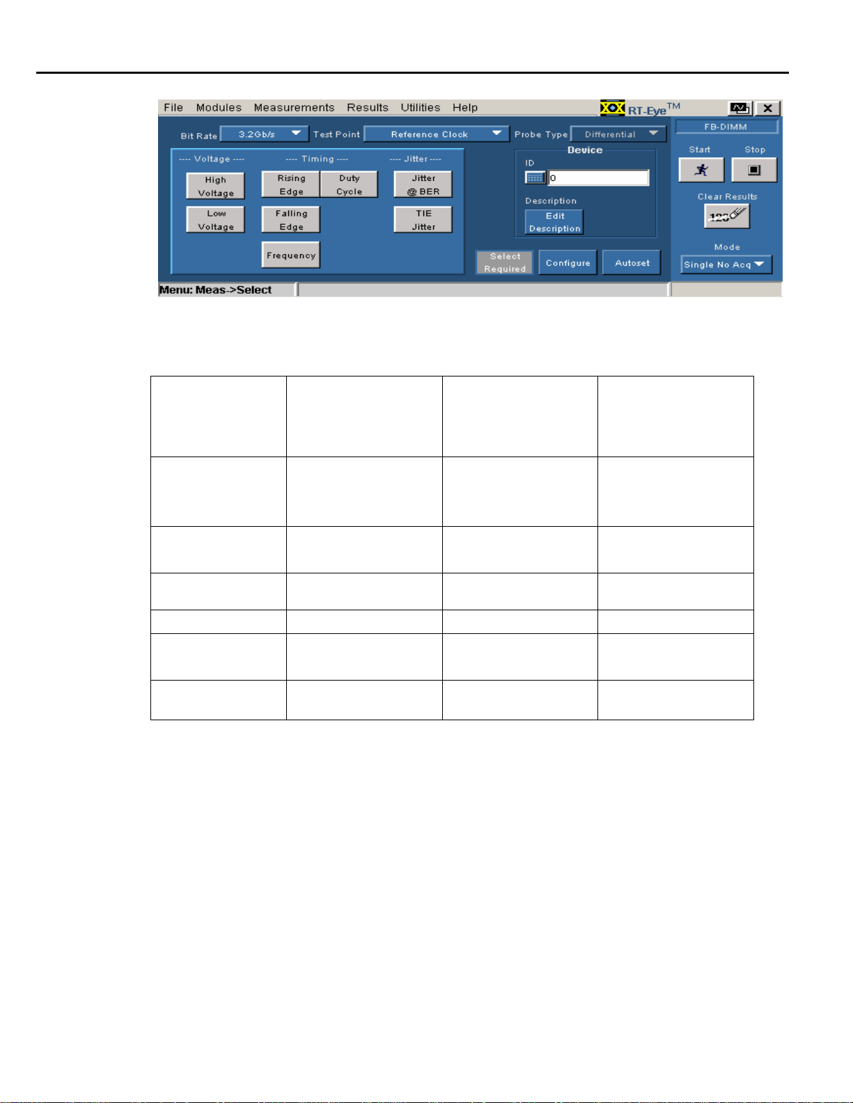
1. Select Measurements> Select.
2. Select Bit Rate.
3. Select Reference clock from the Test Point pull-down list.
4. Select Differential (or Single-Ended) as the Probe Type, depending on your probe configuration.
46 Fully Buffered DIMM (FB-DIMM)
Page 51
Methods of Implementation
Figure 12: Measurements Select menu setup
5. Click the Select Required.
Table 8: Measurement Select/Result Cross Reference (Reference clock Test Point)
Parameter to measure
Reference Clock
frequency @ 3.2Gb/s
or 4.0Gb/s or 4.8Gb/s
Rising and Falling
Edge rates
Differential Voltagehigh
Differential Voltage-low
Duty Cycle Of
reference Clock
Reference clock Jitter
(rms) filtered
fRefclk-3.2
fRefclk-4.0
fRefclk-4.8
ERRefclk-diffRrise,
ERRefclk-diff-Fall
VRefclk-diff-ih High Voltage High Voltage(min)
VRefclk-diff-il
TRefclk-Dutycycle
TREF-JITTER-RMS
Symbol(s)
Selection in
Measurement > Select
Menu
Frequency Frequency (Max,Min)
Rising Edge
Falling edge
Low Voltage
Duty Cycle
Jitter@BER
Measurement Results
Rising Edge (Max,Min)
Falling edge (max,Min)
Low Voltage (Max)
Duty Cycle (Max,Min)
Jitter Random (Rj)
6. Click Configure to access the Configuration menus and set up Signal Source.
Results in
Summary
7. Click Autoset to auto set signal and reference levels.
8. Click Start.
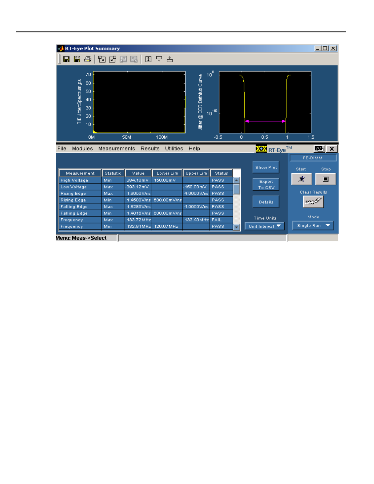
Figure 13 shows the result of a reference clock compliance test on a signal that passes the Reference Clock
tests.
Fully Buffered DIMM (FB-DIMM) 47
Page 52
Methods of Implementation
Figure 13: Result of a completed compliance test at the reference clock pins
6.2.1 Reference Clock Frequency Measurement Test MOI
Test Definition Notes from the Specification:
Reference clock frequency is measured for each data rate of operation.
-This is measured with SSC disabled. Enabling SSC will reduce reference clock frequency.
-Compliance to frequency specification is only required for those data rates supported by the DUT.
Limits:
fRefclk-3.2 : Min = 126.67 MHz ; Max = 133.40 MHz ; Nominal = 133.33 MHz
fRefclk-4.0 : Min = 158.33 MHz ; Max = 166.75 MHz ; Nominal = 166.67 MHz
fRefclk-4.8 : Min = 190.00 MHz ; Max = 200.10 MHz ; Nominal = 200.00 MHz
Test Procedure:
Follow the procedure in Section 4.7 (Draft Specification), ensuring that reference clock frequency
selected in the Measurements> Select menu.
is
48 Fully Buffered DIMM (FB-DIMM)
Page 53

Methods of Implementation
Measurement Algorithm:
The reference clock waveform period is calculated and the frequency is derived from the period
measurement.
Freq = 1/T period
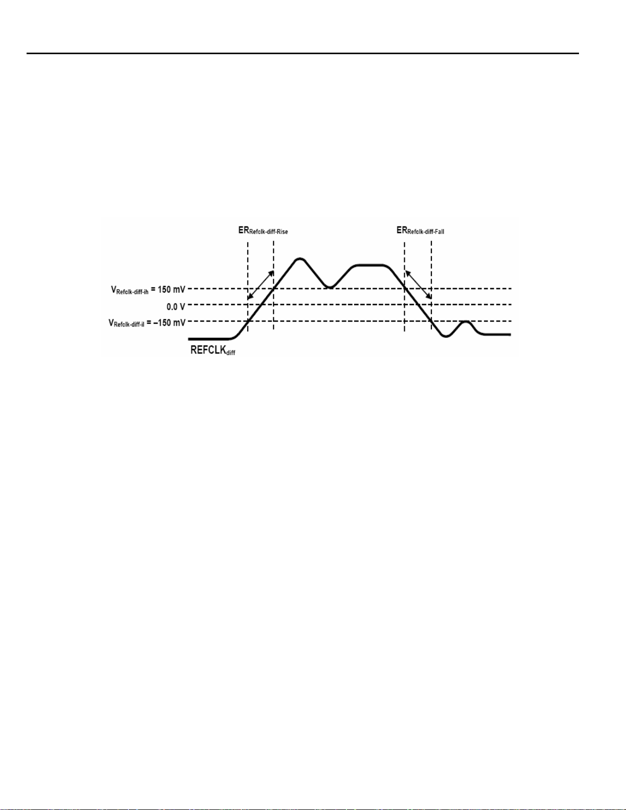
Figure 14: Reference Clock
Fully Buffered DIMM (FB-DIMM) 49
Page 54

Methods of Implementation
6.2.2 Reference Clock Differential Voltage Hi and Lo Test MOI
Test Definition Notes from the Specification:
Differential Voltage Hi and Differential Voltage Lo measurements are taken from differential
waveforms.
Limits:
Vref clk- Diff -Hi Minimum = +150 mV.
Vref clk – Diff-Lo Maximum = -150 mV.
Test Procedure:
Follow the procedure in Section 4.7 (Draft Specification), ensuring that Reference clock differential
voltage Hi/Lo is selected in the Measurements> Select menu.
Measurement Algorithm:
Hi voltage < 150 mV = Fail
Lo Voltage > -150 mV = Fail
50 Fully Buffered DIMM (FB-DIMM)
Page 55
6.2.3 Reference Clock Differential rise and fall edge rates Test MOI
Test Definition Notes from the Specification:
The rising and falling edge rates measurements are taken from differential waveforms.
- Measured from -150 mV to +150 mV on the differential waveform. The signal must be
monotonic through the measurement region for rise and fall time. The 300 mV measurement
Window is centered on the differential 0 V crossing.
Methods of Implementation
Figure 15: Reference clock rise/fall time calculation
Limits:
Minimum = 0.6 V/ns
Maximum = 4 V/ns.
Test Procedure:
Follow the procedure in Section 4.7 (Draft Specification), ensuring that Rise Time/Fall Time
in the Measurements> Select menu.
is selected
Measurement Algorithm:
The rising edge and falling edge are calculated over the 300 mV window, which is centered at differential
0 V. The rising/falling edge rate V/ns = 300 mV/Rise/Fall Time.
Fully Buffered DIMM (FB-DIMM) 51
Page 56

Methods of Implementation
6.2.4 Reference clock Duty cycle Test MOI
Test Definition Notes from the Specification:
The duty cycle measurement of reference clock is taken from differential waveform.
Limits:
Minimum = 40%
Maximum = 60%
Test Procedure:
Follow the procedure in Section 4.7 (Draft Specification), ensuring that duty cycle
Measurements> Select menu.
Measurement Algorithm:
Duty Cycle = positive pulse width / clock period
This is measured at differential 0 V reference voltage level.
6.2.5 Reference Clock Jitter RMS Test MOI
Test Definition Notes from the Specification:
Different devices may have different phase jitter1 tracking behaviors due to variation of the jitter transfer
function of their PLLs, transport delays between transmitter and receiver, differences in the propagation
delays in the devices and the phase tracking bandwidth of the clock phase recovery circuitry.
For the FB-DIMM channel to function properly when the transmitter and receiver use devices with
different phase jitter tracking behavior, a specification of the reference clock jitter spectrum is necessary.
To measure jitter on the reference clock and translate this directly into a data eye closure at the receiver,
the reference clock phase jitter is filtered by a phase jitter transfer function that represents the worst case
mismatch between transmitter and receiver’s phase tracking. After convolving this frequency domain
filter with the reference clock phase jitter spectrum, the peak-peak jitter is measured in the time domain.
As this is a total jitter specification that includes both deterministic and random jitter components, the
sample size is also specified to meet the link’s BER goal.
is selected in the
• Measured with SSC enabled on reference clock generator
• Measured after phase Jitter filter
Limits:
Maximum = 3 ps (3.2Gbps and 4.0Gbps)
Maximum = 2.5ps(4.8Gbps).
52 Fully Buffered DIMM (FB-DIMM)
Page 57

Test Procedure:
Methods of Implementation
Follow the procedure in Section 4.7 (Draft Specification), ensuring that Jitter@BER
Measurements> Select menu.
Measurement Algorithm:
Refer to Specifications section 3.1.3.A second-order PLL transfer function is used as an approximation
for transmitter and receiver. Actual PLLs used in typical CMOS processes are often third order or higher
order. However, all can be approximated as a second-order transfer function. The transfer function
assuming second-order PLLs with PI control loops is defined by the following s domain equation:
In this equation, ζ1/2 are the damping factors for PLL 1 and 2, and ωn1, n2 are the natural frequencies for
the PLLs 1 and 2. This function is not meant as a requirement for an implementation. It is used as a
bounding function for modeling purposes to establish the limits for f_3 dB frequency and maximum
peaking.
7 Giving a Device an ID
is selected in the
The FB-DIMM Compliance Module provides a graphical user interface (See Figure 4) for entering a Device
ID and Description. Data entered here will appear on the compliance report and is recommended for device
tracking.
8 Creating a Compliance Report
To create a compliance report, select Utilities> Reports. The Report Generator utility can create a complete
report of the compliance test.
Fully Buffered DIMM (FB-DIMM) 53
Page 58

Methods of Implementation
54 Fully Buffered DIMM (FB-DIMM)
 Loading...