

Page 1
'
?-
ά
Page 2
COMM
ITTED
TOEXCE
LLENCE
Tektronix,
P.O.
Box
B
υ
erton,
ea
070-2655-00
P
ro
d
uct
Group 75
Inc
500
Oregon
PL
EAS
ECH
AT
THE
INSTRUCTION
.
97077
R
E
E
C
K
A
ROFTH
F
O
RCHAN
IS
SerialNum
MA
G
NUAL
M
ber
EIN
FORM
*
A
NU
F
irstPrintingNOV
R
evised
MAY
ATIO
A
1982
N
L
1979
Page 3
Copy
r ight
Conte
n tsofthis
formwit
ProductsofTe
by
T
istered
Prin
arereserved
Copyrigh
L
meque ce
Τουτ
les
d
I
caractέr
logiques
houtthewr
U.S.
andforeignpatentsand/orpending p
EKTRON
econ te
έροsβα
mprim!
IX,
tra
demarksofTe
te
dinU
t©1979TEK
nu decemanuelnopoutέt r
soit
lesprodu
logotypes
.
αυχ LISA.T
istiquesetprixcla
.
1979
®
.S
Tektron
pub
licationm
ittenpermissionof
n
ix,
ktro
ΤΕΚ,SCO
.A.Specification
.
sansΙ'acco
its
TEK
Inc
rddeTektronix
TEK
T RONIXτοητbrevet
T RON
EKTRONIXserβ
ix,
Inc.Allrights
ay n
otbereproducedin
and
itssubsid
.
BILE,
PE-M
O
ktron
ix,
Inc
andpricechangeprivileges
TRONIXINC.
IX,
n s lecadr
ereproduitsousquelquefor -
ΤΕΚSCOPEMOBI
e
k
Te
ia r
ies
and
.
Τουτdroitsrβ serv6s
Inc
.
έsUSetEtrangeret
serveledr
de dέ
velo
reserved.
t ron
ix,
Inc
.
covered
are
atents
.
a
r
ereg-
LE,
T&
oitdemodifie
ppements
techno-
any
τοητ
Copyright©1979
h
alten.DerInh
νοηTektronix,
P
ro
sinddur
P
atenteabge
TE
W
Ge
b
leibenvorbeh
.
©1979
r
durchTektron
altdieserPublik
Inc
.nicht
dukteνοη
KTRON
arenzeichenνοηTek
drucktin
TEKT
ιάτη
~
kρι
~h`~
Tektronix,
chUS-
undAuslandspatenteund/oderschwebe
deckt.
IX,
ΤΕΚ,SCO
U.S.A
alten.
X
κΓαtUhIfτ~ΗQ
RONIX,
=
τεΠ
η ~
ΤΕΚ
ΗΑ=~τ~i~s
τ
i
N
9 I
ix,
atio
weiteιgegebenwerden.
Inc.und
PE-MOB
tronix,
.
Spezifikations-
,
SCO
τ
1
#IR
ndartohneGe
seinenTochtergesellsch
I
LEand
Inc
.
PE-MOBI
;Έ ~Cι~ι~#
ι
t<
MP
#
Inc
.
AlleRechtevoι
si
nd geschotzte
undPreisAnde
TIόI'fλε
V,
LE,
τ
~~
ο
χ
Tt
neh
3τ4
be-
mig
ung
afte
nde
rungen
n
Page 4
L
ISTOFILLUSTR
ATIONS
TA
. . . . . .
BLE
. . . . . . . . . .
P
O
age
ii
F
CO
Section 3
N
T
EN
T
HEORYOFOPER
TS
F
G
ATIO
504
(SNΒ
N
. . . . . . . .
040000
P
&
age
3-1
UP)
ISTOFTABLES. . . . . .
L
Section1SPECIF
Section2OPER
En
FrenchVer
GermanVer
J
THEFOLLOWINGS
AREFORUSEBY
ONLY.TOAV
NOT
PERFORM
THAN
INSTRUCTIONS
QUALIFIED
ICATION... . . . . . . . . . . . .
ATINGINSTRUCTIONS
glishVer
sio
apaneseVersio
OID
THAT
CONTAINED
TO
DO
. . . . . . . .
sio
n
n
sion
n
W
ARNING
ERV
IC
QUALIFIED
PERSONA
ANY
S
UNLE
SO
.
. . . . . . . . .
E1N
STRUCTIO
PERSONNEL
LINJURY,DO
ERV
ICINGOT
IN
OPER
SS
YO
. . . . . .
HER
ATI
ARE
U
N
NG
iii
1-1
2-1
S
Section 4
Section5MAINTENANCE.
Section
Section7
Section8
Section9
CALIBRATIONPROCEDURE
P
erforma
AdjustmentProcedure
6OP
TIONS
REPL
DIAGRAMSANDILLUSTR
REPL
nceC
. . . . . . . . . . .
ACEA
BLE
ACEA
BLE
heck
. . . . . . . . . . . .
ELECTR
MECHANICALPARTS9-1
. . . . . .
. . . . . .
ICALPARTS
. . . . .
. . . . .
. . . . . .
ATIONS
. . . .
. . .
. . .
. .
4-1
4-3
4-8
5-1
6-1
7-1
8-1
REV
ΜΑΥ
1981
Page 5
F
G
504(SNΒ
F
ig
.
No
.
2-1
2-2
2-3
2-4
2-5 Trigger SignalAmplitudeRequirements
2-6
2-7
2-8
2-9
2-10
2-11
2-12
2-13
2-14
2-15
2-16
2-17
040000&UP)
L
IST
FG504
FG504In
FRONTPanel
SweptFrequencyRanges
SweptFrequencyRange
toVC
andTriggeringPoints. . . . . .
Ph
W
B
SineWaveforms..
R
V
L
L
N
Gated
Triggered
Ph
Ph
AmplitudeModu
FunctionGen
stallation
F1Ν
connector. . . . . . . .
aseRelations
aveformsandTRIGOUT
asic
Functions.Square,
amps
andPulses
ariableRiseandFall
i
near
Sweep.. . . . . . . . . . .
ogarithmic
arrowBand
aseCon
ase
Sweep. . . . ...
Sweep
Operation
Operation. . . . . . . . . . . . . . .
trolOp
LockedLoop
erator
andRemoval.. . .
Controls
h
ips
betweenOutput
. . . . . . . . . . . .
. . . . . . . . .
Times
. .
. .
. . . . . .
eration
Operation
lation
. . . . .
. . . . . . . .
andConn
.
. . . . .
wit
h 10
W
Tria
. . . . . . . . . . . . .
. . .
O
FILLU
ectors.2-3
. . . . .
Vapp
. . . . . ..2-4
. . . . . . ..2-8
aveform
n
gle,
and
. . ..2-8
. . . . . . .
. . . . . .
. . . . . . . .
. . . . . . . . .
. . . . . . . . .
. . . . . . . . .
. . . . . . . .
. . . . . . . . .
. .
. .
lied
. .
. . .
P
age
2-1
2-6
2-8
2-8
2-9
2-9
2-9
2-9
2-10
2-10
2-10
2-10
2-11
viii
ST
F
ig
No
2-18
2-19
2-20
2-21
2-22
2-23
2-24
4-1
5-1
5-2
8-1
8-2
8-3
8-4
8-5
8-6
8-7
R
ATIO
.
.
Supp
ressed
L
owFreque
Delayed
ToneBurst
L
inear
L
ogarithmic
P
ulseSh
Amplitu
SemiconductorBasi
R
ear
Thefollowingillustratio
d
iagram
SemiconductorBasing
A
dju
Α
3LoopBoa
Α1M
(FRONT)
Α1MainBoard
(BACK)
Α
2 Fu
Α
4 F
L
ocations
Operation.. . . . . . .
Sweepof
apingCapabilities
deF
Interface
pull-out
stment
ain
B
oard
nctionBoardCom
loatingInterfaceBoard
N
S
CarrierOp
ncyHoldO
Testing
Sweepof
latnessCheck
Connector
eration... . . . . .
p
eration. . . . . . .
. . . . . . .
F
ilters
. . . . . . . . . . . . .
F
ilters.. . . . . . . .
. . . . . . . . . . .
ng
. . . . . . . . . . . . .
Assignments..
ns are
section
.
. . .
. . . . . . .
. . . . . .
locatedint
Locations
rdComponentLocatio
ComponentLocations
Compo
nen
tLocations
ponen
Componen
t
. . . . .
. . . .
ns
L
ocations
t
. .
he
P
age
2-11
2-11
2-11
2-12
2-12
2-12
2-24
4-11
5-4
5-5
Α
REV
ΜΑΥ
1981
Page 6
Table
1-1
1-2
1-3
4-1
5-1
5-2
L
IST
No
E
r
icalCh
lect
E
nvironmentalCharacteristics
Ph
ysicalCh
TestEquipmentRequ
R
elative
Damage.. . . . .
M
aintena
®
F
aracteristics
aracteristics
ired
SusceptibilitytoStatic
. . . . . . . . . . . . . ...
nceAids
. . . . . . . . . . . . . . . . . .
TA
BLE
. . . . . . . .
. . .
. . . ...
. . . . . . . . .
. . . . . . . . . . . .
. . . . .
. .
. .
. .
. . .
. .
Discharge
. . . ...
. .
F
G
504(SNΒ040000&UP)
S
P
age
1-1
1-7
1-7
.
4-1
5-3
5-9
Page 7
O
T
h
n eral
but
life
may
.
safety
or other
statements
onE
e
ge
p
ersonnel.Specific
apply,
InThisManual
TIONstatements
CA
U
equipment
W
ARNING
loss
of
AsMarked
PER
not
quipment
ATO
informationinthispartofthe
warnings
appearinthis
identify
property
identifyconditions
R
S
SA
and
cautions
summary
conditionsorpracticesth at
.
FE
TY
summary
willbefoun
.
T
ERM
orpracticesth at
S
d
S
UMM
is
for bothoperati
t
h
roughoutth e
could
couldresultin
ARY
result
FG504(SNΒ040000
ng and
manualwh
indamage
personalinj
servicing
ereth
tothe
ury
& UP)
ey
or
CAUTIONindicates
mar
k ing,orαhazard
DANGERindicatesαpersonalinj
h
In
T
is
Manual
This
found
AsMarked onEquipment
DA
Ο
P
rotective
ΑΤΤΕΝΤΙΟΝ
symbol
.
NGER
α p
ersonalinj
property
to
indicateswh
-Highvoltage
grou
n d
-
refertomanual
uryhazard
includingtheequ
uryhazard
h)terminal
(eart
immediately
SY
MBO
ere
applicable
.
.
n ot
immediately
ipment
accessible
LS
cautionaryorot herinformationisto
.
accessibleasone
itself
.
as one
readsthemar
reads
k
t
h
ing
be
e
.
P
ower
Source
T
h
isproductisintendedtooperatefrom
rms
between
p
rotective
essential for
the
ground
safe
supply
operation
conductors
connection
by
.
α
power
betweeneither
or
way
ofthegrounding
sourcethatwill
supply
conductorinthe
not
apply
conductor
morethan
andground.
power
cord
250volts
Α
is
Page 8
F
G
504(SNΒ
040000&UP)
GroundingtheProduct
T
hisproductisgrounded
electrical
pro
conductor
Danger
Up
kn
obs
U
seth
U
se
U
se
For detailed
Refer
shock,
ductinputor
inth
ArisingFrom
n
lossoft
o
andcon
e P
roperPower
t
he p
only
only
αpower
information
cord
and
plug
output
e p
heprotective-ground
trolsthatmay
ower
cord
connector
throug
t
he p
ower
terminals.Αprotective
ower
cord
L
ossofGrou
Cord
cordand
thatisin
on
htheground ing
cor
d
is
essential
appear
conn
good
power
ch
anges
conductorofthepower
i
n
to α
properly
for
n
d
connectio
be
insulating)
to
ector
specified
condition
cords
and
toqualifiedservicepersonnel
wiredrece
groun
safe
operation
n
,
accessible
all
for
.
connectors,
connection
d
can
render
your
see
ptacle
.
product
cord.To
before
by
conductiveparts
an
.
t
hepower
.
connectingtot
wayofthe
electric
module
shoc
avoid
grounding
(including
k
.
manual
he
.
U
setheProperFuse
avoid
fire
To
sp
ecifiedinthe parts
R
efer
fuse
Do
Not
Το
ανο
~d
sp
ecifically
DoNot
To
avoidpersonalinj
applypower
hazard,
rep
lacement
OperateinExp
explosion,donot
certifie
OperateWit
to
d for
the
use
onlythefuseofcorrect
for
list
to
q
losive
operateth
suc
h
out
Covers
ury,donot
plug-in
yourproduct
ualified
Atmospheres
h
via α plug-in
o
p
eration
operate
servicepersonnel
isproductίη
.
.
t
h
is
extender
roduct
p
type,
anex
without
.
voltage
.
p
losive
rating
atmosphere
covers
orpanels
andcurrent
unless
installed.Donot
ratingas
ithas
been
Vi
REV
ΑAPR1980
Page 9

S
ERV
ICI
N
G
SA
FE
TY
S
UMM
ARY
FG504(SNΒ040000
& UP)
F
O
DoNotService
not
Do
rendering
U
Dangerous
touchexposed
Disconnectpower
P
T
rms
protective
essen
perform
se
Care
ower
Source
h
isproductisinte
betweenthesupply
tial
first
Wh
en
voltages
ground
for
safe
internal
aid
RQU
Alone
ServicingWithP
connectionsandcomponentswh
ALIFIED
R
efer
also
serviceoradj
resuscitation
an
d
exist
before
n
d
edto
conductors
connection
operation
to
severalpointsinthisproduct.To
at
removing
operatefromαpower
.
S
ERV
IC
the
preceding Operators
ustmentofthisproduct
ispresent
ower
On
protective
or
between
by
way
of
grounding
the
.
panels,
E
PER
SO
Safety
ilepowerison
soldering,orreplacing
sourcet
either su
h at
pp
conductorint
NNEL
Summary
un
less
avoidpersonalinj
.
will
not
ly
con
ONLY
another
apply
d
uctor
h e
.
person ca
ury,
com
morethan
andground.
power
cordis
p
able
not
do
p
onents
250volts
Α
of
.
Page 10

Page 11
Page 12
Page 13
Page 14
Page 15
Page 16

The
FG
504 Function
Generator
.
Page 17

Introduction
T
sine,sq
frequencies
user-definable
The
open
an
load.Theoutput
swept
wit
h αlinearorlogarit
ph
ase
he outputwaveform
T
triggeringwaveform.T
form
output
bu
tto
Α
the
output
selectedfrequen
onthepolarity
selectedoutput
amplit
nal
504FunctionGenerator
heFG
uare,
triangle,
from0.001
custom
outputamp
circuit
betwee
locked
may
maybeheld
labeledHOLD
n
voltage-controlled
output
fre
ud
source
litudeis10
and 5
im pe
nthe
gated,ortriggered
,
alsobe
frequency
quency
e modulatingthesin
.
varied.Forthe
cy,toα
an damp
freque
STARTand
at
can
SPECIFICATION
provides
ram
Hz
freque
mVto15Vpeak-to-
da nceis50Ω.
h
mic
may
he
any
.
frequency(VCF)input
fromanexternal
ncy.P
pulsewaveformsoverthe
p,and
to40MHzinten d
ncy
range
30Vpeak-to-peakinto
mVto
STO
sweep.The
forsin
be shifte
symmetry
slower
level
by push
be
maximum
litudeoftheVCFinputand
t
swe
p
rovisionis
ewave
also
is
peak
The F
P
FREQdial
outputmay
gle
d
±80°
ofthe
fre
ingth
voltage
above
1000
of
also
output
low
G
or
fromanexter-
d istortio
ecades
available
intoα50
may
504
settings
cycle
output.
fromthe
output
wave-
uencies,the
q
n
t
pan
efro
controls
source.T
belowthe
:1,
depending
madefor
.
be
be
he
the
n
fromtheFG504
Α
applications
.
sponse,
gen
Ω
triggeredorph
for
source
poses
Performance
el
FG504
+20°C
temperature
noted.
above
p
erforming
varietyofsweptand
Th
e
as
distortion,
eration,
variousram
Th
as α
ase-locked
p orpulse
amplitude
for
.
Co
e
followi
ng
calibratedatan
is
and
+30°Cand
between
d
Force
+40°C.Allow
air
verificationtests
Section1-FG
modulate
ma
testingamplifierorservo-system
and
beat
S
PE
nd
itions
electricalcharacteristics
circulationisrequiredat
esp
ke
it
stability
frequency
logicin
waveforms.Itisalso
modulatedsignals
CIFICATIO
ambient
is
0°C
and+50°C,
α one-h
our
.
(SN8040000&
504
signals
d
ecially
operatedat
useful
Itisuseful
.
oscillator,
terface,oras α source
N
temperature
unless
warm-up
as α gated
for
various
are
an
tem
period
for
useful as
valid
ot
p
available
b
ambient
herwise
eratures
UP)
suc
re-
for
pur-
ifthe
etween
before
h
fm
α
F
reque
ncy
R
ange
Si
ne-wave, sq
and
R
amps,
waveformsreq
variable
.5Χ10'
MUL
selectedtiming
acteristic
C
ha
r
uare-wave,
triangle
pulses,orwaveforms
uiring
MME
osition
TRYcon
of
cap
acitor)
SY
Duty
Cycle
p
TIPLIERswitch(User
use
of
trol
ELECTR
.001Hzto40MHz
in10
ICA
LCHAR
P
erformanceRequirement
overlapping
Table
calibrated
ste
1-1
ACTERISTICS
ps
SupplementalInfor
.001
Hz to
n
ominally
_<7
ο/οto>93ο/οbelow1MH
<20°/οto
=400
capacitorprovidesαfull-scale
frequencyof-=400Hz.The
factory-installe
α 20Hzto
.5Χ10'position
theMULTIPLIER
>80
ο / ο
above
kHzmaximum.Α5μF
capacitor
d
20 kHzra
of
switch.
4
MHz
1MHz
nge
mation
.
z
gives
forthe
Page 18

Specification-FG
504
(SN
Β
040000&UP)
Table
1-1
(cont)
haracteristic
C
F
requency
R
esolution
(cont)
Stability
Time
Temperature
Dial
Calibration
Dial
Accuracy
FREQUENCY
d
ial
STOP
FREQuencydial
M
aximumFrequencyRanges
Dial,
Sweep
Voltage
F
requency
Frequency,
Controlled
(VCF)Modes
H
z
(START)
and
for
P
erformanceRequirement
<-0
.05
ο/ο
for10minutes
for
/ο
for
scale
(START)
1hour
24 hours
full
MHz
from4MHz
the
the
start
plus
dial
scale
from
.Within6ο/οof
40
MHz
to
difference
and
stop
the
FREQUENCY
error
.
M
aximum
<-0.1ο/ο
-<0.5ο
W
ithin3ο/οof
0
.001Hzto4
full
W
ithin5ο/οof
b
etween
frequencies
Hz
MULTIPLIER MinimumFreq-
Setting
106
5
-10
10
10
10
1
1 ,1,10-1,10-
-s
1
encyRatios
500
->1000
->100
40
:1
:1
:1
:1
Supplemental
1
partin10"offull-scale
setting
usingthe
control,asmeasured
frequency
counter
Information
FREQUENCY
with
.
VERNIER
α
Appliestocalibrated portionofthe
Hz
dial
only
FREQUENCY
The
instrument
constant
b
etween
c
hecked
See
Dial
mustbeatα
ambient
0°C
temperature
and
+50°C
afterα1-hour
Accuracy
.
and
warmup
.
1to40Hz(ΧMULTIPLIER
setting)
(ΧMULTIPLIER
M
temperature
.
after
STOP
uncalibrated
MULTIPLIER
calibrated;0.1to
easurements
between
1hour
warmup
FREQuencydial
setting)
madeatan
the106
on
range
.
1
uncalibrated
+15o
CC
.
is
Hz
ambient
and
.
+35'C
to
Internal
Sweep
Accuracy
Sweep
Stop F
requency
Swept
Stop
F
requencyError
LINear
Duration
SWEEP
to
0Vto
+10
L
inear
orLogarithmic
L
imitedbyStart
F
requency
external
greater
Specifications
frequency
accuracyisrequired
100sto0.1msin
(selectedbySWEEP
V
ARiable
W
ithin2ο/ο
sweep
W
ithin
control
from
duration
/ο
from1msto0.1ms
10
ο
sweepduration
V
.
Output
impedance1kΩ.
.
and
Stop
;use
counter
six
decades
URATION
D
overlaps
100sto1ms
.
.
if
.
switch)
decades
.
.
Page 19

Table
1-1
(con
t)
Specification-117G
504(SNΒ040000
&
UP)
Internal
Sweep
TPUTAmp
OU
Accuracy
WEEP
S
V
oltage-controlled
Freq
N
TR
Input
L
M
n
se
evel
aximumInp
uencyInp
ominalSen
(Hz/volt)
M
aximumFrequency
M
inimumFrequency
(cont)
litude
IGgerINPU
sitivity
ut
(VCF)
ut
sitivity
1
hin5ο/οfrom
W
it
W
ithin10ο/ο
from
100 s
msto0.1ms
1
to
ms,
.
T
=4ΧMULTIPLIER
volt.Α
i
ncreases
M
range
for
V
M
ositive-going
p
frequency
aximum
frequencydividedbyVC
(seeMaximumFrequency
Dial,
SweepFreq
oltage
Controlled
odes)
.
setting
per
voltage
.
uency,
F
and
requency(VC
R
anges
F
F)
R
ate
Slew
Input
Impedance
OUTPUTSignal
F
latness
Sine-wave
0
.001Hzto
kHzto40MHz
40
Triangle
0
.001Hzto
40kHzto40
u
S
q
are-wave
0
.001Hzto20MHz
20MHzto40
Si
ne-wave,
an d
S
M
atc
h
Amplitude
40kHz
Triangle,
uare-wave
q
40 kH
MHz.
MH
Amplitude
At
least30Vρ-ρi
circuit,
W
ithin±0.5dB
W
ithin±2dB
to40MH
least15Vinto50Ω.
at
z
.
.
from
nto
40
an
kH
open
z
Typically
z
40
.Referenceat10kHz
MH
hin±0.5dBto
wit
.
z
z
R
eferenceat10
R
z
eferenceat10kHz
kH
.
.
Page 20
Sp
ecification-FG
504(SNΒ040000&UP)
h
aracteristic
C
Table
1-1
(cont)
P
erformanceRequirement
S
upp
lementalInfor
mation
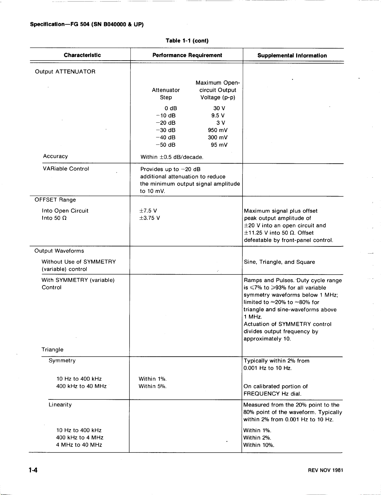
Output
ATT
ENUATO
Accuracy
VA
Riab
leCon
OFFSETRange
Into
O
pen
Circuit
I
n
Ω
to
50
OutputWaveforms
W
it
h
outUseofSY
(variable)
control
trol
R
MME
TRY
Atte
nu
ator
Ste
p V
0
dB
-10
dB 9.5V
-20dB
-30dB
-40
dΒ
-50
dB
W
ithin±0.5dB
P
rovides
add
itional
t
he mi nimumoutput
/decade
-20dB
up
to
attenuation
to10mV.
±7.5V
±3
.75
V
M
aximumOpen
circuit
Out
oltage
(p-p)
30
V
3
V
950mV
300mV
95mV
.
to re
duce
signalamp
p
ut
litude
-
M
aximum
peakoutputamplit
±20
±11
d
efeatablebyfront-panelcontrol
Sine,
Vin
signalplus
toanope
offset
ude
of
n
circuitand
.25Vinto50Ω.Offset
Triangle,and
Square
.
W
ithSY
MMETRY
Control
Tria
ngle
Symmetry
10Hzto
400kHzto40
L
inearity
10
Hz
400kHz to4MHz
4
MH
400kHz
400kHz
to
zto40
(variable)
MHz
MHz
W
ithin1ο/ο
W
ithin5ο/ο
Ramp
s a
nd Pu
is
<_7
ο/οto>93
symmetry
limitedto
triangle
1
MHz
waveforms
-20%
andsin
.
Actuationof
d
ivides
output
lses.Duty
ο/ο
for
to
e-waveforms
SYMME
frequencyby
cycleran
all
variable
below1MHz;
~80%
for
TRY
control
ge
above
approximately10.
Typically
0
.001
Hz to
withi
10Hz.
n 2
ο/ο
from
.
.
On
calibratedportion
FREQUEN
M
easured
80ο/ο
within2ο/ο
W
ithin1
W
ithin2ο/ο
W
ithin10ο/ο
CY
fromthe 20
p
n
toft
oi
from0.001Hzto 10Hz.
ο/ο
.
.
.
of
Hzdial
.
ο / ο
pointtot
h
e
waveform.Typically
he
REVNOV1981
Page 21

haracteristic P
C
OutputWaveforms
Sine-Wave
TotalHarmonic
Distortion
20Hzto40kHz
40kHzto1
1
MHz
Sq
uare-wave
ANDFALL
RISE
F
IXED
Aberrations
VARiable
(cont)
MHz
to40MHz
TIMES
Table
1-1
(cont)
erformanceRequirement
<-0.5ο / ο
.
h
Greatest
30
dBdown
Greatestharmonic
20d8down
_-6
measured
_-5%ρ-ρplus
10nsto
M
easuredbetween
90%pointsofAmplitude;accuracy
within
10Χrange
armonic
.
.
ns 10nsto100
from
100
30%.VARiable
.
10%to90%
mV
30
in
7
ms
at
least
at
least
msin7
into50Ω
steps
the
10%
controlhas
steps
load
.
and
Specification-FG
Supplemental
Typically
20Hz,
measured
conditions:Temperature
+35°C
into50Ω;zero
attenuation,
FREQUENCY
between
Applies
.
ambient
P
eriodof
combinedrise
by
%20
ο/ο
504
(SNΒ040000& UP)
_<1
ο/ο
from0.001Hz
un
terminated
offset;<_30
and
with
H
z
(START)dial
4and40.
topulse
.
waveforms
waveformmust
and
Information
der the
+10°C
dB
exceed
fall
times
to
following
to
set
also
.
AM
INPUT
Dc
4
MHz
Input
E
xternal
ΦLOCK
Input
Sensitivity
M
aximum
TRIG
to 4
MHz
to40MHz
Impedance
TRIG/GATE/
Input
Impedance
LEVEL
M
inimumPerio
Input
Amplitude
d
5Vρ-ρ
modulationofα
with
modulation
~10
modulation
_<1Vp-P.
-1Vto
signal
<_5%
οdistortionat70ο/
.
/οdistortion
ο
.
+10V.
prod
sine-wave
at65ο/ο
uces
100ο/ο
carrier
ο
When
driven
imped
ance
<_600Ω.
M
odulating
to20kHz
bandwi
dulating
mo
_<10kΩ
modulation
put
amplitude
_>1ΜΩ.
>_10kΩ
+20V
F
or
triggeringαsingle
of
generator
75ns.
frequencies
.Modulation
dth
isdoto
source
ensures
.
.
fromαsource
100
im
proper
an
d d
ivides
by2.
waveform
from
frequency
kHz.Α
pedance
the
cycle
.
20Hz
of
out-
REVNOV
1981
1-5
Page 22

Specification-FG
504
N
8040000& UP)
(S
Table
1-1
(cont)
C
E
xternalTR
ΦLOCKInput
GAT
ΦLOC
IG/GATE/
M
aximum
F
requency
E
Minim u
M
aximum
Frequency
K
h
aracteristic
(cont)
Trigger
mPerio
Gate
n
P
erforma
_>20MHz
d
ceRequirement
.
75ns
Su
.
lemental
pp
Information
d
+20
MHz.
100Hzto40MHz
range
Hz
to4MHz.
±80°
Adjust
0
100
.
from
For
gating
of
generator
Capture
sions
range:±10ma
from
majordial
40
MHz
(40
but
will
trac
multiple-cycle
waveform
100Hzto
ivisions
d
from 4
MHzmaynot
k
.)
burst
.
or
dial divi-
j
4MHz;±8
MHz
cap
ture,
to
4MHzto40MHz
LockR
ange
PHASE
Ph
aseAdj
MAN
TRIGOU
H
OLD
TPUT
Drift
R
ange
ustmentRange
±8majordial
+2Vfrom50Ω
0Vto
0
.001Hzto400Hz.
divisions
.
will
Generator
external
lockto
signal,
thePHASEcontrol,
majordial
4MHz andwithin±1MH
to
divisions
from4MHzto40MHz
from0.001Hzto4MHz.
±80°
Manual
pus
Trigger/Gate
h
button
.
wit
hout
α ch
angi
rea
dju
within
±10
from
100Hz
z
.
front-panel
ng
sting
.
ρ-ρ
output
10ο/ο
of
amplitude/hour
.
REV
NOV
1981
Page 23
Table
1-2
S
pecification-FG
504
(SNΒ040000&UP)
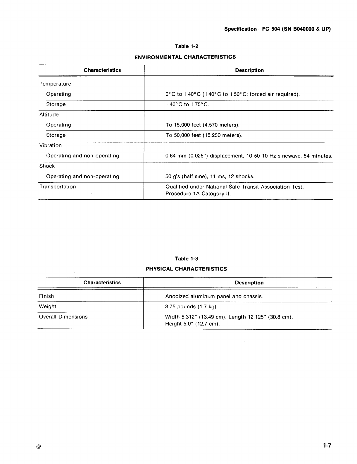
Temperature
Operating
Storage
Altitu
de
Operating
Storage
V
ibration
Operating
Shock
O
perating
Transportation
C
haracteristics
andnon-operating
and
non-operating
ENVIRONMENTAL
C
HARACTERISTICS
0°Cto+40°C
-40
1
Cto+750C
To
15,000
To
50,000
0
.64
mm
50
g's
(half sine),11ms,12shocks
Qualified
P
rocedure1Α
(+40°Cto+50°C;forced
.
(4,570
feet
feet
(15,250
(0.025")displacement,
underNational
CategoryΙΙ.
meters)
meters)
Safe
Description
air
required)
.
.
10-50-10Hz sinewave,54minutes
.
Transit
Association
.
Test,
.
F
inish
W
eight
Overall
Dimensions
C
haracteristics
PHYSICAL
Table
C
HARACTERISTICS
A
nodized
3
.75
pounds(1.7
W
idth5.312"
H
eight
1-3
aluminum
5
.0"
kg)
(13
.49
(12.7cm)
Description
panel
and
chassis
.
cm),Length12.125"
.
.
(30.8cm),
Page 24

Section
2-FG
504(SNΒ
040000
UP)
&
I
N
STA
LL
I
T
he FG504
received.It
ΤΜ
500
series
ower
t
he
p
requirements
coolingisrequired
degrees
ce
Turnthe
removing
herear
at
t
useful
lifeofthe
donetothe
is
eratesinany
o
p
power
module
and p
n
tigrade
power
t
h
e F
interface
plug-in
O
PER
ATIO
N
G
NANDREM
ST
RU
CTIO
calibrated
modules
instruction
ower
mo
for
eration
o
p
.
ule
mo
d
;oth
504
connectors
erwise,
connectors.Arcing
circuitry
ATI
NS
and ready
two
compartments
except
manual for
d
ule
operation.
off
before
arcing
and
.
N
OVA
to
theTM501
line
between
inserting
may
reduces
damage
G
L
use
of
.Refer
voltage
Forced
40 and
occur
t
may
INST
w
h
en
t
he
to
air
50
or
h
e
be
RU
heck
C
t
he p
of
t
here are
outsin
i
ndicate
may
anothertypeof
thishas
Whentheunits
wit
hthe up perand
selected
partment
interconnectingjacks.ThePO
luminate
To removetheFG504,
locatedonthe
edge
connectors
ks.TheFG504
j
ac
CTIO
for
plastic
barriersont
ower
modulein
barrierspresent
heFG504
t
special
instrument.Donot
been
verifie
arep
compartments.InserttheFG
andpress firmly to
henthepower
d
w
lower
disconnect
will
heselected
t
andthey
circuit
board
rearin
d
byqualified
roperly
lower guides
module
pullthe
left
corner,
now
slide
N
S
interconnectingjack
he
compartments.If
donot
edge
connectors,
terface
matched,
seat
WER
fromthe p
out
connections
insertthe
servicepersonnel
aligntheFG504
(seeFig.2-1)ofthe
504
thecircuit
lightsh
switchis
release
untilthe
t
hepower
of
matc
h
the
plug-in
the
into
boardsinthe
latch,which
circuit
ower
com-
ouldbe
turnedon
boar
mo
module
s
cut-
they
for
until
.
il-
.
is
d
d
ule
.
REV
ΜΑΥ
1981
Fig.
2-1.F
G
504
Installatio n
and
R
emoval
.
En
glish2-
1
Page 25

Operating
Output
The output
50Ωvoltage
frequencies,anunterminated
output
waveform
less
E
termination,
(especially
waveformpurity,
1
tors
Instructions-FG
O
PER
ATI
Connections
of
source
will
cause
(see
ImpedanceMatching d
than 50Ωwill
xcessive
.Use
.
distortionoraberrations,
are
with
good
N
G
CONSIDERATIONS
the
F
G
504
working
excessive
reduce
less
noticeableatthe
sine
and
triangle
observe
quality50Ω
the
the
504
(SNΒ040000&UP)
isdesignedtooperateasα
into
α50Ω
or
improperly terminated
aberrationsonthe output
waveform
waveforms).To
following
coaxial
load.Athigher
iscussion)
amplitude
duetoimproper
lower
frequencies
precautions
cables
and
.Loads
.
ensure
:
connec-
=10:L
FRED
k
nob
ispulledout
RUN:(Button
H
OLD:(Button
providesanoutputdolevel
signal
frequency
V
output
FREQUENCY
variations
CF
when
INPUT:E
frequency
ampindicates
out)
in)
t
he
ranges
xternally
.
VERNIER
.
.
for
Disables
button
only
normal
.)
when
SYMMETRY
operation
the
generator
equaltothe
waspushed.(5
applied
:
Forfine
levelofthe
voltage
.
and
lower
varies
frequency
2
.Make
all
connections
3
.
Use
goodquality
reduce
avoid
adequatepowerhandling
waveform
coupling
constantofthe coupling
enough
waveform
4
.
Use
terminations
reflections
5.E
nsure
.
If
thereisα do
to
IftheFG
SeriesPowerModules,
form
can
r
esults
fromPowerModule
is
incompatible
p
r
oblemiseasily
personnel
when
that
capacitorinseries withthe
maintain
504isusedinearlymodelsoftheTM500
be
excessiveinsome
for
checking
attenuators
amplitude
or
impedance-matching
using long cable(6feet
attenuators,
voltage
capacitor
p
ulse flatness
NO
withFG
cured.R
tight
and
as
shortaspossible
if itisnecessary
applied
capabilities
across the
ΤΕ
rippleontheoutput
504
transformerph
to
sensitive
terminations,
for
the output
output
and
.
cases
transformerphasingthat
operation;however,the
efer to
qualified
load.The
load
mustbe
.
Th
asing
load,
e
circuits
devices
or
more)
etc.,h
use
time
long
wave-
ripple
service
.
ave
to
to
.
.
.
α
MULTIPLIER
d
ial
.
ί
~
9
Ο
INPUT:E
AM
sine
wave
L
ATCH:Pulltoremove
INPUT:A
locking
MAN
:
or
manual
output
LEVEL:Selects
INPUT
locked
ΦLOCK
cy
to signal
GATE
:Buttonincauses
waveform
tor
.
:Determines
xternally
output
.
pply
external
signalstothis
P
rovidesαmanual
gateinGATEoperationtocontrol
waveform
waveform
operation
:Buttoninlocks
.
the
for
.
appliedtoINPUT
during
αhigh
rangeofFREQUENCY
applied
the
gating,
connector
triggerinTRIG
beginning
triggered,
output
levelatthe
signal
p
lug-in
triggering,
.
voltage
gated,or
waveform
connector
generatortoproduce
.
INPUT
modulates
or
phase-
operation
the
level
on
phase-
frequen-
.
connec-
α
CONTROLS
English
FREQUENCY
tion,orlowest
STOP
FREQUENCY
cyinsweep
2-2
AND
(Hz):Selects
frequency
(Hz)
mode
.
CONNECTORS
frequencyofopera-
in
sweep
mode
:
Selectshighest
.
frequen-
T
RIG
:Buttonincauses
cycleofoutput
INPUT
16
FREE
waveform
waveform
signal
.
RUN
:Buttonincauses
.
generatortoproduce
for
each
positive-going
continuous
REV
ΜΑΥ
one
output
1981
Page 26
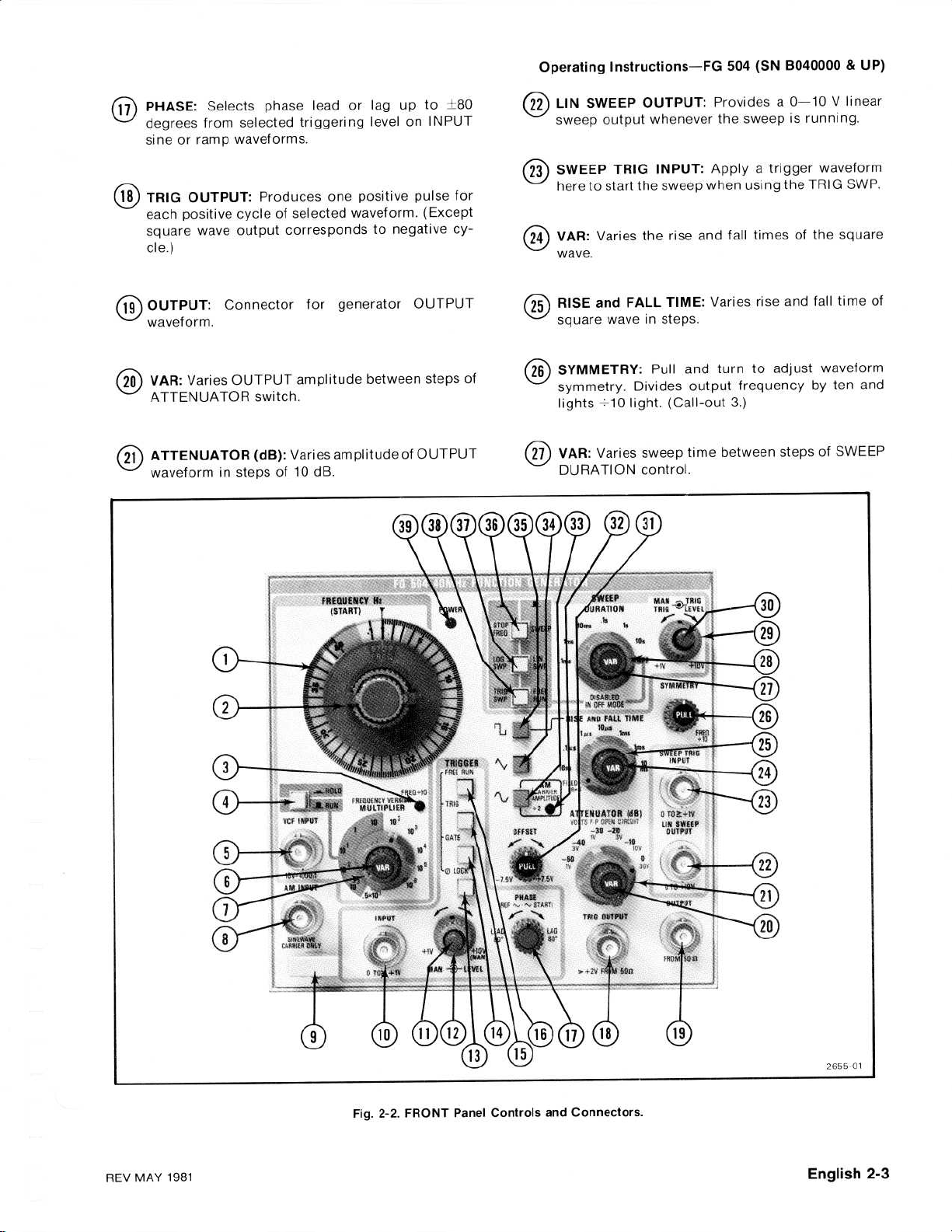
PHASE:
degrees
Selectsphase
from
sineorramp
T
RIGOUTPUT:P
eac
h p
ositive
uare
s
cle
wave
q
.)
selecte
d
waveforms
roduces
of
cycle
output
selectedwaveform
corresponds
lead or
lag
up
triggeringlevelonI
.
one
positive
pulse
. (
to
negative
to
E
=+-80
NPU
xcept
for
cy-
504
(S
N Β
Operating
L
T
sweep
SWEEPTRIGI
h
VAR:V
wave
Instructions-FG
INSWEEP
output
ereto
start
ariesthe
.
O
U
TPUT:P
whenever
NPUT:
t
heswee
rise
rovides
the
sweepisrunning
Apply
p
w
hen usingtheTRIG
fall
and
040000
α
0-10Vlinear
α
trigger
timesofthe square
&UP)
.
waveform
W
S
P
.
TPUT:Connector
OU
waveform
V
AR:Varies
ATTENU
ATTENU
.
TPUT
OU
ATORswitch.
ATOR(dB) :Varies
waveforminstepsof
generatorOUTPUT
for
amplitu
d e
betweenste
amplitudeofOUTPUT
10dB
.
R
IS
E an
d FA
LL
square
s
of
p
SYMME
symmetry.Divides
lights
V
VAR
:
ATIONcontrol
DUR
in
wave
TRY:Pull
=10
light.(Call-out3.)
aries
sweeptime
TIME
steps
:Varies
.
and
output
.
rise
turn toadj
frequency
between
stepsofS
and
ust
fall
time
waveform
by
ten
WEEP
of
and
REV
ΜΑΥ
1981
F
ig.2-2
.FRO
NTP
anelContr
olsandConnectors
.
En
glish2-3
Page 27

O
p
erating
Ζ
6
Instructions-FG
S
WEEP
D
UR
sweeping
ramp.
ATION:
504
(S
N8040000
Selectsdurationoffrequency
&
UP)
For
first
time
operation,
B
lue
section
:
preset
thecontrolsasfollows
:
T
RIGLEVEL
that
MAN
when presse
OFFSET:Pull
31
waveform
AM
CARRI
impedanceatAM
(SINEWA
33
(T
RIANGLE
wave
(SQUA
35
Ο
output
starts
sweep
P
TRIG
:
from
ERAMPLITUDE
VE):B
output
.
RE
WAVE)
.
:
Selects
rovides
d
W
levelonS
ramp.
manual
i
n
.
and
rotate to
0Vat
I
NPU
uttoninselects
A
VE)
:
B
utton
:
theOU
T
<_10 kΩ.
B
utton
in
=2
WEEPTR
sweepwaveform
offset
TPUT
:Lamplights
sine
in
selects sq
IG
theOU
connector
wave
selects
uare
INPUT
start
TPUT
.
when
output
triangle
wave
FREQUEN
(Main
STOP
MULTIPLIER
H
O
LD/
R
V
A
Green
FREE
Orange
S
WEEPDUR
U
nmar
.
SineWave
R
IS
ATT
V
A
R
Connectα50Ω
vertical
V
ertical
Horizontal
Dial)
RUN
section:
RUN
section
ked
section:
Ean
d F
ENU
ATO
i
nput
CYHz
:
N
ATIO
ALLTIME
R
bnc
oscilloscope.Set
of
an
time
base
cable
10
40
10
1
RUN
(out)
ully
F
cw
In
O
FF
In
FIX
D
E
-10
F
ully
cw
terminated
the
oscillosco
1V/Div
1
DC
millisecond/Div
in50Ωtot
pe to
coupled
he
:
STO
P
FRE
highest
frequency
Q
UEN
CY
L
OG
g1
sweep
T
start
free
P
T
heCon
of
t
he front p
determining
functioncontrols
internal
orange
SWP/LI
logarithmic
.
R
IG
SWP/
withtrigger
run.
O
WER
:
F
G
504
.
F
IRST
trols
anel
controls
swee
pfu
on
t
he F
B
uttoninsto psfrequency
D
:
(STOP)
dial
Indicates
and
controlsand
n
G
frequency
from
STARTtoSTO
.
N
SWP:
sweep
.Button
FREE
RUN:B
.Button out
whenpower
TIME
Connectorspages
andinputs
ction
504
O
are outlinedin
are
controlsand
front
panel
PER
connectors.Thefrequency
sweep
.Button
out
P settingsonFRE-
B
utton
outproducesαlinear
utton
outlinedίη
.
inprod
i
n
causes
causes
is
ATIO
inputsare
N
give
blue,
green,and
sweep
thesweep
applied
α d
escri
the
outlined
sweep
uces
ption
trigger
t
he
at
s
to
to
to
in
A
djust
theoscillosco
cyclesofthe
wave,
sine
unmarked
R
otate
theATT
t
he out p
cond
t
he c
OFFSETk
F
sq
switc
to
c h
wave,
push
p
osition,
N
fre
L
OG
slowatfirst
butto
fre
k
nobon
ut
itions.Pull
h
ange
P
ress
thesquare
A
LL
TIME
uare
wave
h tothe
its
outpositionand
ange
of
and
ed
in.Retur
W
it
hthethree
switc
ote
that
quencytoα h
SWPbuttonin
n and
quency
the
sinewave.Now
wave,
and
the
section
amplitude
nobtothe
andobserve
ENU
ATO
changes.R
out
theOFFSETknob
indolevelofthe
i
n position
wave
switc
hth
roughits
sha pe.Return
PRE
SETposition.
rotate
waveshape
t
h
e
sine
for
wave
ntheSYMME
buttons
htheSWEEP
the
output
ig
her
frequency
and
and
then
more
note
that
thesweep
of
the
sweep
maindial
i
ntheblue
pe to display
alter
nately
tria
ngle
t
he
R
andVAR
eturn
output
.
button
in the
frequency
note
range.R
i
range
t
he
Pull
it throughits
the
square
with
t
he
TRYknobtoits
orange
D
UR
onceαsecond
that
thefrequency
rapid.Press
secitonoft
at
least
five
pushί
η
t
he sq
uare
wave
buttonsint
d
ifferent
controlstoverify
waveform
n
.
R
.Note
R
IS
theSY
approp
ATIONswitc hto1s.
changes
stops
otate
waveshapes
that
themtothepreset
and
rotate
otate
Eand
range
wave,
sectionintheout
the
theSTO
it
.Retur
R
t
he
t
he ch
FALL
MME
TRYknob
.
the
riate
inposition.
from
.
P
changeis
STO
at
t
hehigh
he panel
.
N
otice
nthe
ISEan
ange
TIME
Note
triangle
buttons
α
low
ress
P
FRE
P
FRE
.
Note
full
he
of
t
he
t
he
Q
est
Q
.
d
En
glish2-
4
REV
ΜΑΥ
1981
Page 28

t
h
at
theSTO
R
elease
theSTO
button.Note
theMAN
h
anges
c
OFFposition
once.R
FRE
P
Q
is
P
FRE
Q
button
that
thefrequencynolonger
TR
button
IG
eturn
t
heS
.
by
set
and
andnote
WEEPDUR
theSTO
press
that
ATIO
P
FREQd
the
TRIG
S
n
ges
N
k
nobtothe
.Press
cha
thefrequency
WP
ial
.
pedan
loss.Signal
can
pulse.It
shortaspractical
OperatingInstructio
ce,
velocity
loss
is
attenuatehighfrequency
is thereforeimp
ns-F
of
pro
p
relate
dtofrequency.Α
.
ortant
G
agation,
informatio
504
to k
N
Β
(S
and
amou
fewfeetofcable
nin α
eep
these
040000
n
tofsignal
cables
&
UP)
fast-rise
as
P
ress
theTRIGbutton
in
.Note
that
the
OU
buttoninthe
p
lete
com
p
ressed
button
t
h
e
MAN
again
for
T
he out p
V
ary
the
output
Kn
ob
selects
d
ial.Switc
t
he sign
pus
hthe
to
see
waveformand
buttonisreleased
This
ment
.
R
isetime
If
the
the
riseorfalltimeofα d
ch
aracteristics
risetimeofthedeviceundertestisatleast
than
thecombined
monitoring
introduced
ignored
than
ten
testing
determined.
compone
e
q uals
individual
O
n
ce
of
t
he d
preceding
The
transmitting
gree
output
.Press
.Note
buttonispressed.
continuous
cycle
theGATEbutton
theoutput
that
ut
frequency
FREQUEN
frequency
al
H
that
completes
andFalltime
output
.When
timesaslongasthe
system,
n
thesquare
risetimes,or:
therisetimeofthesystemisk
evice
physical
.
thefrequency
hthe
MULTIPLIER
amplitudeslowly
O
LD/
RUN
oscillator
the
then
.
pulse
of
oscilloscopeand
will
not
theriseorfalltimeofthetest
t
he actual
T
h is is
t
ma
king
R,
under
method
and
cable
in thegreen
TPUT
signal
n
section
inand
for
eachtime
waveformiscontinuous
Press
output
.
controls
CY
controltosee
T
h
output
e
rangecoveredby
varies
buttonin
stops
begi nsatthesame
thefirst
t
h
e
exceed1ο/ο.
root of
_(
.
time
from
t
he F
evice,
associated
risetimes
associated
risetimeofthe
nd
from
fou
thesystem.The
up
thesum
R
ι
) Ζ
test
canbe
electricalcharacteristicsofthe
determine
section
stops
note
theMAN
i
n
.
Now
the
FREE
are
fre
quency
k
nobtothe
on
and
release
at
operation
G
504isuse
consider
equip
of
t
he
This
error
combinedrisetimesoft
the
of
R
~
z ) Ζ
+
foundby
thecharacteristic
.
Press
that
thereiso
pressthe
RUN
outline
theeffect
MULTIPLIER
10
- Ζ
the
oscilloscope,
it
several
one
point
poi ntwhen
of
d to
therisetime
ment
ten
times
F
G
504
cables,
can
generally
deviceisless
system
risetime
total
t
he s
q
uaresoft
+
. . .
nown,
t
he pan
of
theMAN
switchis
MAN
while
button
d
i
n
blue
t
on
main
the
range.As
times
on
t
t
theinstru-
measure
used.
If t
longer
plus
the
the
error
must
of
eac
risetime
the risetime
using
t
pulse
im-
ne
he
he
he
he
be
he
be
he
he
When signal
el
in
d
ifference
the
identical
Impedance
Asαpulse
en
countersαmismatch(or
thatofthe
sent
.
p
olarityofthereflectionsare
pedance
matchis
reflectionwillbeof
Ifitisαlower
willbeof
If
it
addstoor
distorts
If
ΜΩ
1
itance) of
transmission
an
dth
t
he input
prop
F
reeRunningOutput
Select
by
UA
SQ
P
h
us
D
UR
d
esired
Q
UEN
controlpermits
load
buttonis
desiredpeak-to-peakoutput
k
nob
Thewaveforms
offset
for
thedesiredoffset.Ifαsquare-wave
adjust
values
determi
d
evice
test
loss
transmission
k
along
bac
mismatc
α
opposite
t
he reflected sign
the
t
he F
G
input
t
heverticalinp
en
theoscilloscopeinput.The
capacitance
erly
terminated
t
he d
pus hingthe a
REWAVE,
h
th
e
FREE
ATIONswitc
frequency
CYHz
t
h
to
e
out.Set
vary
to
thewaveforms,
theR
T
h
.
eVA
compariso
n
ations
should
and
time
M
atching
travelsdownαtransmissionline,
theli
ne tothe
h
en
h ig
her
value
the
value
tha
polarity
subtracts
pulseshapeand
504
impedance
line
isdriving
to α50Ω
esired
TR
from
.
waveform
IANGLE,
RUN
h
is
wit
(START)dials.T
finefrequency
OUTPUT
theATT
t
he
amplitudebetween
with
ISEan
d F
R
k
nob
n
measurements
are
made,
the
two
signals
travel
throughcoaxial
delaycharacteristics
an im
pedance
line),αreflectionisgeneratedand
source.Theamplitude an
determinedby
countered.Iftheimpedance
t
h
am
am
e
before
p
p
litu
(s
q uare,
or
FF p
line
edance,
litu
d
button
SI
NEWAVE
than
same
polarityast
nthe
lineimp
.
al
returns
the
αhighimped
(paralleled
uttoanoscilloscope,
attenuator,50Ω
t
h
of
e device,and
pp
ropriate
button.Make certain
in
theO
.
d
ifferent than
impedance,
he a p
pliedsignal
thereflectio
t
he pulse
d
t
he pu
e of
e
.
ance
byαstated
termination,
attenuator
t
heF
triangle,
mar
t
osition.Select
h theMULTIPLIERandFRE-
he
FREQUEN
adjustments.Connect
terminal
out
pulland
ALLTIMEcontrol
offset
varies
.Make
ENU
ATO
amplitude
center
rotate
these
CY
certain
R co
n
trol
.Use
the
steps
around0V.To
theOFFSET
out putis
for
thedesire
times
between
or
cables
eachtime
theim-
is
ended
lse.This
suchas
capac-
connectt
isolates
504
G
or
sine)
ked
symbols
he S
WEEP
VERNIER
t
he
H
for
theV
.
control
selected,
time
from
with
mis-
t
t
wit
t
t
OLD
t
A
t
he
he
h
he
he
he
he
it
d
.
n
,
e
is
h
.
R
d
REV
ΜΑΥ
1981
E
nglish2-
5
Page 29

Β
Operati
control
selectedwaveform,
co
t
waveform
button.The
outputs
sinewaveform
feature
output
variesthe
Pull
any
Triggered
ngInstructions-FG
steps.Αtrigger
nn
ector
.
usingthesineor triangle
Wh
en
heMULTIPLIER
output
waveform
αdovoltage
reac
not
does
Whenpulled
frequency
based
time
controland
this
thet
of
W
hree
or
Gated
it
hthe FG504
is
inthe
may
equaltot
hed
erateonthesquare
o
p
out,the
(FRE
symmetry
turn
basic
Operatio
set for
describedintheprevious
or
gating
signal
outputwaveformper
of
the
TRIG button
triggeringwaveform
begin.Ifmore
desired,
now
pressthe
beginsatthe
waveformatthei
inglevel.T
gating
waveform
proximated
ap
periodofthe FG504
of
operation,
theterminationofthe
If,
at
app
roximately
ditional
variesthe
±80°
p
control
as
cycleiscom
in
triggeredor
startoft
T
h
.
is
ointontheoutput
Toman
ually
fully
d
desire
.IntheTRIGmode,
triggersone
mode,the
the
MAN
butto
V
oltage
α
ControlledFrequency
T
he output frequencyofthe
frequency
MULTIPLIER
theI
to
and
setth
at
t
han
one
GATEpushbutton
triggeri
nputcon
he output
durationisnowthe d u
.
The
bydividing
outputfrequency
t
he FG504
270°
of
p
gated
triangleorsine
he
h
asechangeis
p
waveform
trigger
k
wise
cloc
cycleoft
selectedoutput
n
ispressedin
range
setting,by applying
504(SN
signal,
one
availableatthe
slowest
b
e
stopped by push
generator
he
w
henthebutton
MMETRYcontroldividesthe
SY
Q
=10ind
ofthe
forthe
waveforms
free
paragraphs,apply
NPUTconnector.If
trigger
LEVEL
e
whic
control
hthe output
cycleofthe
ng
level
nector
numberofcyclesper
gating
the
always
gati
thelast
leted.
eratio
op
measure
.
or
gatetheFG
andpus
he outp
htheTRIG
ut
waveform
.
1000
of
040000&UP)
for
eac
h cycle
TRIGOUTPUT
waveform
output
fivepositions,th
ingthe HOL
t
stopsa
nd
he FG504
voltagethetriangle or
waspushed
.
n,and
waveform
icator
selected
desired
waveform
lit)byte
symmetryusi
.
n
running
operation
the
only
isdesired,
forthe
levelonthe
triggering
e
οη
pus
waveform
output
waveform
.TheFG
504
output
an d continues un
drops
belowthe
trigger-
ration of
b
urst
may
signal
duration
. 1
ηthegate
completes
ng
waveform,
d
thelast
lessthan
cycle remains,an
nthePHASEcontrol
output
waveform
d
504,
hingtheMAN
pus
fromth
e 0V,0°
nthe
tur
GATEbutton
or
waveforms.Inthe
continuesaslo
Operation
FG504
:1,
α 0Vto
ca n be
depe
swept
nding on
10Vsignal
t
he
of
wit
This
.
ng
as
cycle
hthe
is
to
he
til
t
t
he
be
he
byt
mode
cycle
ad-
LEVEL
button
GAT
ngas
over
the
by
D
is
h
e
to
t
heVC
imum
necessarytovarythe
obtai
nthe
frequency
10
6
10
5
ί7
Ζ
10
°
f-
ω
.
10'
ω
l7
10
2
Ζ
α
σ
σ
ω
J
α
10-' ~
J
Σ
10
-2
10
-
'-
Fig.
2-3.Graphsh
MULTIPLIER
appliedtoth
The p
d irectio
.
E
setbytheMULTIPL
cy
an d
FREQUEN
voltage
voltage
symmetrically
symmetrically
thefrequency
Sincethe
linear
d
mine
Hzd
ialposition
setting
maximum
n
ominal
setting.Forexample,
two-voltchangeatt
frequency8kH
Custom
This
frequency
T
FINPU
vcfrangefor
connector.SeeFigure
eachMULTIPLIER
FRE
:1
full
desire
ustom
C
swept rangeorthelowest
1000
d
.
positionwithfactoryin
UEN
Q
CY
4kHz
400 Hz
40
Hz
20
Hz_
4 Hz
4
0
0
0
0.4Hz
.04
.004
.001
10-'
setting
eVC
Hz
:
Hz
Hz0.4Hz
0
.04
Hz
Hz
10-210-'
owing
that
FINPUT.
4
11010210'
can be
4
0 Hz
Ητ
Frequency
r
ange
swept
400
of
olarityofthevcfinputsignal
ntheoutput
CYVERN
thefre
raises
frequency
I
ER,
IERcontrols.Αpositive-going
quency
swept
is
FREQUEN
while
lowersthe frequency.
V
about
about
controls
inputamp
vcf
sweeps theoutput
0
the cen
ter frequencydetermi
(seeFigure
litude
relationship,thefrequency
fromthe
timesthe
(40)
V
CFinput
sensitivity(H
Timing
feature
vcf
.
VC
z
.
permitsthe user
amplitudeandthe
input
Fsen
sitivityistheh
MULTIPLIER
voltage
z p
er
V)
wit
h α
heVC
FINPUTwillchanget
Ran
ge
V
(10
.
4timestheMULTIPLIER
of
10'
to
range.The.5Χ10'
2-3
setti
VERNIER
themax-
for
ng.Itmay
control
swept
dcap
stalle
80kHz
acitor.
40
4
MHz
MHz
400kHz
4
0kHz
20
kHz
4 kHz
Hz
10410510610'108
Hz
2028-03
frequenciesforeach
sig
wit
h α0to10V
n
determinesthe
fromthe
CYHz
α n
Α
voltagethatvaries
fre
quen
R
(STA
egative-goi
freque
T),
ncy
ned by
2-3)
.
output
ighest
ra
nge d
frequencyisα
maybe
FRE
Q
deter-
UEN
CY
possibledial
ividedbyt
versus
).Inthe FG504,thisisa
MULTIPLIER
setting,
heoutput
installαcustom
position ofthe
swept
MUL-
be
to
al
-
ng
he
α
En
glish2-6
REV
ΜΑΥ
1981
Page 30

OperatingIn
structions-FG
504(SNΒ040000&UP)
Τ1PLIER
installed
MULTIPLIER
20kHz
Ph
ch
switchis
capacitor
.
aseLocke
Th
e
frequencyoft
ronized
used
(C248)
switchprovides
dOp
eratio
wit
h an
externally-applied
forthe
custom
forth
α
n
he outp utwaveform
swept
range.The
isposition
range
reference
from
may
factory-
ofthe
20Hzto
be
syn-
signal
Th
e
output
frequencyoft
±10maj
applied
division).Connectthe
connector
control
respecttothereference
controladju
waveform
.
ordialdivisionsofthe
signal(the
andpus
variesthe ph
.
heFG
504mustbe
frequencyofthe
"1"onthedialisthelowestmajordial
ststhe
reference
hth
e
ΦLOC
aseofthe
triggeri
signal
signaltotheI
K
pushbutton.ThePHASE
output
waveform±80°
waveform.TheLEVEL
ng pointonthe
settowithin
externally
NPU
wit
reference
T
h
Fig.
P
roperadj
easier
FREE
t
hanthe
I
NPUTconnector,andthen
LEVELcon
t
he
an
oscilloscope)adj
FG504untilitisnearlythe
signal
controlat12
pressΦLOCK
to
obtainαstable
controlrange
Αjumper
modulatinginputw
REV
ΜΑΥ
ustmentoftheLEVELandPHASEco n
ifthey are adjustedfirst
RUN
frequencyoftheFG
frequencyoftherefere
trol
for
stable
ustth
appliedtotheI
o'clock
.
R
decreases
allowsth
1981
NPUTconnector.SetthePHAS
(for0°withsine
dj
ustthePHASE
ea
output atthe desired ph ase.ThePHAS
eVC
henthe FG504isoperatedinthe
2-4.Sweptfr
intheTRIG
504
nce
signal
selecttheTRIG
triggeri
e output
sameasthefre
above4MHz.
FINPUTto
ngand(if
control,ifnecessary,
equencyrange
mode.Setthe
somewhathigher
ap p
mode.A
frequency
quencyofthe
wave
selected)
functionasα phase
trols
liedtot
viewing
ofthe
with10Vsignalap
he
dju
on
an d
is
st
E
E
plied
toVCFIN
PHASELOCKmode.Thephase
limits
are±2.5
Whenp
the
Amplitude
themod
t
dial
AmplitudeModulatingInputspecification
mation
h
outputphase
To
amplitude
heSI
NEWAVE
for
aboutthismode
loc
ase
M
ulating
t
h
e
V,
odulating
signaltotheAMINPUTconnector.Push
d
esiredcarrier
conn
ector.
modulatingi
wit
h anup
ked,thephase
by approximately
modulatetheoutput
pushbuttonand
per
Input
of
operation.
frequency
modulating
setthe
frequency
5°/V.
waveform,
FREQUEN
nput
limit of1kH
voltage
connect
R
efer toth
.
for
morein
En
glish2-
voltage
z
varies
Hz
CY
for-
.
e
7
Page 31

&
r
ating
Ope
Internal
WEEPDUR
S
sweeptimes
(STA
desired
linear
SWP
U
se
frequency
t
he "1"
Sweep
Select
R
T),
swept
swee
pus
t
he
FREQUEN
calibration figureonthe
desired,pus
trigger
Adjust
desired
o
sig
t
erationis
p
he
levelont
Instructions-
Operatio
thetime
ATIONcontrol
STO
p
hb
utton.R
when
htheTR
n
altotheS
LEVEL
d
for
between
FRE
P
frequencies.Select
rate
bypus
elease
CY
sweepi
IG
control
triggeringwaveform
he
esired,
F
G
504
n
one
.Use
steps.Set
an
d
Q,
hing or
theSTO
VERNIER
from
ng
S
WP
WEEP
release
(SNΒ040000
complete
theV
t
TIPLI
MUL
eitherαlogarit
releasi
control
frequencies
dial.if
pushb
utto
T
R
IG
so
t
he
TRIG
t
he
sweep
R
A
FREQUEN
he
ER
ngthe
P
FRE
to set
atriggered
n
andconnect
I
NPU
sweep
.Iffree
SWPpus
UP)
with
k
nobtoobtain
CY
for
d
ials
h
mic
L
OG/
Q
button
pus
h
h
e
STA
t
lower
sweep
T connector
at
starts
running
h
button
t
he
H
the
LIN
RT
than
t
t
or
he
he
z
.
is
.
.
The
swee
p
any
time
at
li
near
swee
connector
E
xternal
L
k
,andSwee
oc
E
xternal
1Vρ-ρ
(+1Vto
mi
+0
amplitudeis
must
signals
n
imum,
.5
Vand+1
beatleast
around
areasshown
may
be
stopped
hin
g
Signals
TrigModes
p
signals
thedo
.For
V
3Vρ-ρ
theSTO
htheLEVEL
signal
example,
i
n F
bypus
voltageisavailable
p
.
Input
input
+10V).Wit
theexternal
.5
symmetrical
and
t
he
P
for
Trigger,
h
ese
for
t
voltage
setbythe
must,
about
(+1
.5Vto-1.5V).
igure
2-5
output
fre
FRE
Q
pushbutton
at
theS
WEEP
Gate,
modes
must
control
at least,
externalsig
an
0V(suchas
.
quency
LEVEL
pass
α
Typical
h
.The
OUTPU
Ph
ase
beatleast
control
at or
near
h
roug
t
n
al
whose
sine
wave)
input
eld
T
h
F
ig
.
points
+1.5Υ
(min
.)
+0.5V
O
V
+1
.SV-
(min
.)
O
V
+10
V
(+1.5V
min.)
O
V
2-5.Trigge
.
~
r
Signalamp
--------
___-____
-
-
litu
d
erequir
LEVEL
+1VtO+10V
LEVEL
+1V
LEVEL
_
+1V
ements
(mi
to
ndtriggeri
a
TRIG
W
aveform
n
+10
.)
OUT
V
2028-38
PU
ng
T'
2-7
Fig
.
waveforms
.BASIC
selectedby
FUN
CTIONS.Squ
fro
n
tpanelpushbutto
are,trian
ns.
gle,and
sine
'Dutycycle
d
uty
*Alsoram
F
ig.2-6.Ph
th
eTRIG
E
nglis
cycle
h
oftheTRIG
of
sorpu
p
ase
T
O
U
2-
8
theOUT
relationships
waveform
lses
PU
u
.
TPUT
OU
T
waveform
singtheSY
betwee
waveform
.
MME
TRYco
nOUTPUT
gle
Tria
n
W
aveform*
Sinewave
uarewave*
Sq
t
follows
he
2028-39
n
t rol
.
waveformsand
Fig
b
asic
.
2-8
waveforms
R
AMPSAND
.
by
usi
SES.Thesear
PUL
ngtheSYMME
TRY
eob
cont
tai
nedfrom
rol
REV
t
he
.
ΜΑΥ
1981
Page 32

Fig.2-9
andfall
formed
.VARIA
BLE
timesinthesquare
.
RISEAN
DFALLTIMES.By
wave
mode
r
va
ryingthe
va
ious
pulseshapes are
rise
Operating
F
ig.2-11
2-10.Selectth
logarithmic
available
.LOGARITHMIC
rate.T
.
Instructions-FG
WEEP
logarithmicramp.
e
S
he logarithmicrampvoltage
504
.Use
The
NΒ040000&UP)
(S
t hesame
frequencyisswept at α
setupasinFig.
isnot
exte
rn
ally
F
ig.2-10
andtheinternallinearrampforα
sto
REV
.LINEARSWEEP.Select
i
pfr
equencies
ΜΑΥ
nthe
1981
selected
thestart
swept
time
.
and
stopfrequen
output fro
mthe
start
cies
to
2-12
F
tria
9
u
sweepi
.
ig
.
n
gle
waveform
.52kHzandt
seful
fornar
ng
NARR
ramp
OWB
AND S
sweptbyαlinearr
he stop
row
.
band
frequency
sweep
WEEP.The to
amp.The
10
is
testing.Thebottom
ptraceshowsthe
startfreq
.52kHz.This functionis
t r
En
glish2-
uency
aceist
is
he
9
Page 33

O
p
erating
F
ig.2-13.GATEDOPER
output
appliedtothetr
pushb
thewaveforms
Instructions-FG
waveforms
utto
n p
ressedin
are gate
504(SNΒ040000&UP)
ATION.Theto
t
h
and
e
iggerINPUTconn
.Notethe
dof f
bottom
.
tr
aceisthegatingwaveform
additional
pthreetracesar
ectorwit
hthe
cycle
completedafter
e various
GAT
E
F
ig.2-15.PHASECONTROLO
illustratesPHAS
super-impose
T
h is
cont
trace
isthe
dtr
rolprovi
triggering
E control
aces
illustratetheeff
desapp
wavefo
usageinthetriggered
roximately
PER
ATION.Thisphotograph
ectoftheph
rm
±80°ofshift.Th
.
mode.Thefive
asecontrol
ebottom
.
F
ig.2-14.T
various
outputt r
r
m
wavefo
de
selected
mo
is
completed.
E
nglish2-10
RIGGEREDOPER
aces
selected.Th
ap
thetriggerINPUTconnector
pliedto
.Notethatonly one
ATION.Thetopthree
e b
ottom
trace
cycleoftheoutput
t
r
t
hetr
is
wit
arethe
aces
iggering
hthe TRIG
waveforms
F
ig.2-16.PHASE LOCKEDLOOP.Thebotto
ap
pliedtotheINPUTconnectorinthe
operation.Themiddletraceisthe
i
nputsignal.Thetoptracesshowtheeffect of
outputphase lockedtot
mtr
aceisthesignal
ΦLOCKmode
t hePHASEcont
REV
ΜΑΥ
of
he
rol
1981
.
Page 34

F
ig.2-17.A
100ο/οmod
signal.±2
d 0 V)
arou
n
~
~
Ϊι
MPLITUDE
ulatede
voltsmodu
.5
.
! ι
λιιι
Ι
ilj
!il,~~
l
Ι
~
Ι
1~
ΊΊΊΊΙ
MODULATION.Thetop
nvelope andthe
latestheoutp
bottom
ut
t r
aceshowsthe
themodulati
trace
100
ο / ο.(5VΡ-Ρcentered
ng
eratingInstructions-FG
O
p
ig.2-19
F
thelowest
pushingthe
obtainedin
.LOWFREQUEN
five
MUL
LDbutton.The
HO
hismanner
t
CYHOLD.The
TIPLIERsetti
steps
.
ngs
504
can
onth
N Β
(S
output
h
be
time exp
is
eldat
040000&UP)
t
he FG504
of
any
level
osure
were
in
by
UPPRE
Fig
.
2-18.S
shows
e
α
n
velopewhilethebottom
waveform.T
andthe
modulati
suppr
bottom
ng
essed carrie
SSEDCARRIERM
d
ouble
sidebandsu
he upper
peak
waveformmust
roperation.
pp
t r
ace
kofthemodulating
pea
isat-10
be ca
UL
ATION.Th
OD
ressed carriermodulation
displaysthe
V
overall
.
The
u
llyadj
r
ef
etopt r
mo
waveform
levelο1 t
ustedfortru
d
ulating
is at0V
ace
he
e
ig.2-20.DELAYED
F
reavailablebyusing
a
generator.T
1
οtheS
O
UTcon
I
NPU
amount
settingoftheTR
asαdelay
hemi
TRIGI
WEEP
r.Thisrampisapp
necto
Tcon
nector.Thetop
ofdelayispropo
IG
generato
NEEMEMmi
mmli
MENEEME
.
.ν
.
.~,
.*..-~..
.~~
PER
ATION.Αwiderangeof
O
theinternal
dle
t r
aceistheunder
d
NPUT.Th
traceisthe
tionaltotheswee
r
LEVELcontrol
rtosetthe
sweepge
ebottom
liedtothe
.Be sure
STO
P
neratorasα
i
n
put
laye
d
trace
is attheLI
external
delayedoutp
p d
uratio
hen
usingtheswee
w
FRE
d
ial
Q
delay
signalapp
pulse.T
ut
nand
fully
εεω
,
2028-18
times
delay
lied
WP
NS
trigger
t h
.
he
e
p
REV
ΜΑΥ
1981
En
glish 2-11
Page 35

Operating
I
n
structions-FG
504(SNΒ040000&UP)
ToneBurst
The F
usedfor
TEKTR
thetriggerINPU
operation.Setthe
pulsed
sweep
fre
quencies.T
oftone
Testing
G
504,
toneburst
ONIXPG501
uration
andrepetitionrates.Now
time
forthe FG504.Selectthe
he
burstsasshowninFigure
wit
h an
external
testing.Connectth
(or
T
connector.SelecttheGATEmodeof
external
output ofthe FG504
p
ulse
equivalent)
pulse
generator
2-21
generator,
e
output
pulse generato
forthedesire
selectth
will
.
start
ηοω
e
an
be α
may
of
d
esired
d
stop
series
be
α
r
to
d
F
ig.2-22.L
frequencies
inear
sweepshowing skewe
.
d sp
acingof
filteroutput
F
ig.2-21.TONE
ramp
f r
omthe LINSWEEP
F
ilter
Testing
Th
e
swept
q
uite
suitable
FG504inthisapp
Mode.F
using
logarithmic
igures
BURSTTE
frequency
for
2-22and2-23
STING.
OUTPUT
capabilitiesoft
sweep
lication,
sweeps
Thelowertraceisthelinea
terminal
testing
.
filters.Wh
it
is
besttousethe LOGS
illustratethe
.
he FG504makeit
en usingthe
advantages
WP
of
r
Fig.
2-23.L
outputfrequen
oga
rithmic
cies
.
swee
pshowing
eve
nsp
acingsof
filte
r
En
glish2-
1
2
REV
ΜΑΥ
1981
Page 36

P
ulseShap
Theexternal
pulseshaping.Connectthep
triggerINPU
square-wave
wit
htheTRIG
levels,
changedasdesired.Figure
tion
.
ing
triggering
Tconn
mode.Thetriggering
LEVEL
andsymmetry
featureoftheFG
ector
n
a
control.Theriseand
ofthe
504a
ulsetobe shapedtot
d place
clean
2-24
theFG
level
outputpulse
illustratesthisapplica-
504inthe
maybeselected
fall
dap
may
tsfor
he
times,
be
O
p
erating
REP
IftheTek
Tektronix
howi ng:owner
s
individualatyour
complete
the
servicereq
Save
and
wasshipped.Ifthe
n
ot
available,repack
Surrou
protectthefinishoftheinstrument.Obtainαcarton
corrugated cardboardofthecorrect
andhaving
morethanthe instrumentdimensions.Cushio
instrumentbytightly
or urethanefoam
si
des
.
stapler
.
Instructions-FG
ACKAGI
tronix
Service Center
instrument
uired
re-usethe
ndtheinstrument
inside
NGFO
instrumentisto
(wit
hadd
firmthatcanbe
serial
.
packageinwhichyour instrume
original
agetheinstrumentasfollows
dimensionsofηο
pack
betweencarto
Seal
carton
wit
504(SNΒ040000&UP)
RSHIPMEN
besh
ipped
for
service
an dthe
ress)
number
packagingisun
withpolyethylenesheeti
ingthree
n
an d
hsh
ipping
air,
or re
p
attachαtag
name
contacted.Inclu
an d αdescriptionof
fit
carton
less
thansiχ
inc
hesofdunnage
instrument,
tape
or
industrial
for
strengt
T
to
of
use
:
ngto
inches
nthe
on
all
α
an
de
n t
or
of
h
Fig.
2-24.PULSESHAPINGCA
the
triggering
signal
n
T
PABIL
.
ITIES.T
helowe
rtr
ace
is
p
ounds
he carton
.
test
strengthfor
your
instrume
tis200
REV
ΜΑΥ
1981
En
glish2-13
Page 37

Page 38

Page 39

Page 40

Page 41

Page 42

Page 43

Page 44

Page 45

Page 46

Page 47

Page 48

Page 49

Page 50

Page 51

Page 52

Page 53

Page 54

Page 55

Page 56

Page 57

Page 58

Page 59

Page 60

Page 61

Page 62

Page 63

Page 64

Page 65

Page 66

Page 67

Page 68

Page 69

Page 70

Page 71

Page 72

Page 73

Page 74

Page 75

Page 76

Page 77

Section
3-FG
504(SNΒ040000
&
UP)
Introduction
The
followingisα
in
theFG
schematic diagrams
the
manual
Triangle
T
his
capacitors,positive
semiconductor
triangle
The
QUENCY
sweep,
The
(START)dial
potentiometer
(106),
linearityofthe
frequency
U
30A
mode,
t
hrough
control
input
in
the
frequency
voltage,
FREQdial,
amplifier
and
are
summed
3
of
and
from
controlspositive
504.R
aidinthe
to
Generator
circuitry
switchesnecessarytogenerate
waveform
current
Hz
when
calibration
R
128isswitchedinto the
control
.
When
the
sweep
STOPFREQ
sets
ofU25B
swept
an
U
the voltage
U45
and
decreases
155isfedtothe
U
.
sources
(START)
operating
suppliedvia
is
R
145.On
FREQUENCY
theFG
ramp
maximum
the
.
Thisaction
frequency
input
d
t
he
sweep
summed
are
30B
servesasα
from
atpins3of
U155
foranincreaseinfrequency
current
T
HE
description
efer
to
on
the
understanding
orMainLoop
consists
n
egative
and
and
inthe
voltage
thehighest
voltageisfedinto
504
operatesinthe
isfed
controlR5
voltage,
ram
the
45
U
increases
baseofQ165
source
of
the block
foldoutpages
of
α
current
controlledby the
are
STOP
swept
for
the
operational
Hz
operational
to
ramp
setsthemaximum
mode.The
phase
p
voltage,
atpin6ofU25B
level
FREQUENCY
andU155.The
for
α d
transistor
R
Y
O
the
electrical
diagram
this
of
(Diagram
d
iode
bridge,
sources,
controls,aswell as
frequency
FREQUENCY
amplifier
MULTIPLIER
circuittoim p
(START)dial
operational
swept
amplifierU25B
an
d
b
ufferU5A
voltage
voltage
lock loop
throughthe
shifter.These
Hz
ecrease
The
output
.
O
circuits
and
the
back
at
description
1)
timing
and
the
mode
U513
setting
rove
.
amplifier
frequency
lied
ap
voltage
Q55
to the
p
or
upperlimit
controlled
correction
Operational
.
voltages
(START)
at
frequency
in
The
output
.
fromU45
.
the
the
asic
b
FRE-
and
This
.
This
STOP
pins
F
of
the
.
Hz
the
ial
d
PER
O
To un
derstand
loop,
assume
off.Current flows
090
is
throughCR180.Diodes
biased
.
withnocurrent
C
R190.Current
throughdiodes
capacitors.In
tings,
α cap
cap
acitors;switches
opens
Q230,
W
currentdivides
andthe
C210.One-tenth
R204
R
the
ten.The
resistances
d
voltage
the
through
Q255A
constant
Q255A
amplifiers.Transistors
Q285
the
input
the
the
currents
U
This
.
Q225
ith
switches
remaining
charge
to
200
and
effect
iscussion,
betweenpins
action
positive-going
The
.
The
drivesαset
and
emitters
The
ramp
comparator
of
positive
emitterofQ310
375
.
ATIO
operationofthe
the
that
switch
from
CR188
the
slowest
acitance
S240-3
capacitance
and
their
associated
S240-5,
.Most
of
current
of
the
C210
because
R204istentimes
multiplying
of
multiplying
are
added
the voltage
2
ofU215,
R202
otherhalfofthe
current
Q295
of
is
input
forhigh fre
Q225,
to
remain
Q255A.Therampat
to
of
the
other.The
Q280
and
also
fedtothe
amplifierU375
ofU375
uency
q
N
triangle
driver
Q100
the
from
flowing.No
thepositive
an
multiplier
6,
and7closed,
the
current
the
factorisincrease
in
at
and3ofU215
constant
rampisapplied
two
Q270
servestocompensate
negative
CR182
d
C
R186,
five
MULTIPLIER
and9close
multiplier
resistors
current
flows
through
flows
the
the
resistanceofR
valueofC210by
series
pin3ofU215
an d
Q230
buffer,
fet
complementary
and
ramp
Q295
.
base
through
componentsatthe
conducting
is
and
CR184
current
current
charging
replaces
consists
thepositive
flows
R200,
through
combinedresistance
with
remainsatzero
causes
.
to
Q255B,
Q280compose
output
Q310to
of
through
R336.The
generator
an
current
and
through
d
C210.Forthis
rampsup.
the gateoffet
source
back-
are
flows
through
source
and
as
the
flows
the
timing
switch
timing
the
S240-16
of
U
capacitors
timing
R202,
R
204,
R200
202.Thishas
α
factor
additional
the
current
supplies
source
Darlington
one
taken
is
thenegative
R322,
and
waveform
the
inputs
set-
215,
and
and
of
of
The
and
set
from
drive
d
.
of
;
to
at
of
The
SYMMETRY
between
collectorofQ165
mirrorisformedby
matchedpair
emitter-to-base
rents
0165
the
are
equal.This
exactly
positive
of
voltages.Therefore,
matches
control
negative
and
connects
transistors,
to
transistors
ensures
the
collector
adjusts
that
the
current
the
baseofQ175.Α
Q170A,Β,
0170
Α
the
currentofQ175
current
sources.The
and
and
Β
,
their
collector
collector
balance
current
Q175.The
h
ave
equal
current
.
cur-
of
W
iththe
voltage
the
voltage
ramp
positive
baseofswitching
base
direction,
ramp
atpin3ofU375isabout
atpin9.
in
andpin
Q80.As
Q80
the
rises
of
risinginthe
This
makesU375
positive
7negative.Pin7ofU375
transistor
the
decreases
direction,pin6of
ramp
conduction
0.4V
Q65
and
continues
positive
d
irection,
more
positive
inoperative.As
U
connectstothe
connectstothe
pin
6
inthe
and
Q65
the
than
the
375
goes
positive
increases
Page 78

T
heoryof
Operation-FG
504(SNΒ
040000
&
UP)
conductionuntilthepair
from
about-2.8Vto
-2
.8
V
.
This
actiondisablesthe
U
375
anden
conduction,
condution.Curre
an
dthepositive
CR188
throug
hCR
cu
rrent
C
R
184.This
n
egative
output.Astheramp
p
i
n 14
negative.Wh
goes
ficiently
tion,thepositivecurrent
cap
acitors,
Thebases
nn
ectedtothenon-invertingou
co
outp
uts
common
generatethe
S
q
uareWave
Switchingtransistor
Wh
en
collectorofQ65isinits
p
assedtothe
baseofQ456.TheemitterofQ456
When0456isconducti
hCR
wit
andt
he square
the
switching
co n
dution,
movesinth
as
Q470isnotconducting
V
ariableRise
Th
is
sources,
an output
currentsourcewh
source.The
curren
t throug
changingthevalues
T
he
cap
acitors,
R
536,R538,R584,
0540
andQ580
theVAR
co n
trolisi
grou
n
de
current throug
source
integratingcapacitors
waveforms
ablestheupp
Q90
comesintoconductionan
n
andCR
source
gradually
negative,
fromth
the
470bac
circuitry
current
d
transistors.An
186
180asQ100isoff.Current
now
actio
direction,
goes
andth
of
emitter
ese
emitter
T
R
IGOU
Generator
rampis
baseof0450
k-biased.Current
wave
waveform
back-biasingCR
n
egativedirectionby
e
andFall
consists
α currentswitchwit
.
buffer
rise
and
hthe constant
C592throug h C598,isvaried
asnecessary.Thecur
controlth
nthecalibrated
endofthe con
htheemitter resistancesofthecurrent
.
switches.Pin3ofU375
about-3.2Vand
erpair.Wh
t
flowsth
now
ntsource,
curre
are
back-biased.
flowsth
n chargesthe
causingαnegative-going
goesnegative,
p
entherampreaches α voltage su
Q65
turns
epreviously
emitter
amplifiers
Tand sync hron
risingint
ng,Q462isoff;Q470isconducting
movesinthepositivedirectio
Transistor
ile
Q580
fall
of
available
andR
roug hU530
increasein ch
reducesthe
roug
ositive.Pin13ofU375
off,
sourceisconnectedtothe
followers
followersdrivethe
065
generates
most
negative
T
heemitterofQ450drivesthe
.
ch an
ges
462
.
Circuitry
of variablepositive
hin
Q540
servesast
times
arechan
theintegrating
to chargetheintegrati
586intothe
position,the
.Thisactio
trol
now
pin9goestoabout
lowerpairof
roug h Q90,
Q55
h d
timi
t
h
Q80
describedcycle
Q410
tputs
Q415
hepositive
d
rives
flowsth
state,
T
h
.
currentthroughCR470
(Diagram
tegrati
serves asthepositive
curre
and
Q530.Whent
arging
rise
transistorsin
en
Q80
d
Q100
diodeCR
.Bridge
No
current
from
the
iodesCR
ng cap
acitorsinthe
ramp
utp
ut
e
o
comesintoco nduc-
and
izing
state.This
e
square
ng
henegativecurrent
gedbyvaryi
n t
capacitors
rentisalso
andfalltimesoft
of
gradually
and
Q395
ofU375.T
Q406,
signals
t
he square
direction, t
Q462
and
roug hCR
Q462comesin
wave
2)
andnegative
capacitors,
sources
switching
by
emitter
circuit
wiperisat
nin
creasesth
curren
goes
ceases
ceases
190,
dio
des
flows
negative
182
an
t
at
U
375
timi
repeats
are
bases
whic
.
wave
signal is
Q470
462
n.Wh
en
now
and
ngt
and
.
varied
heVA
the
tfort
he
ng
he
he
to
he
by
ng
by
he
he
at
of
f-
of
The
connecte
Q495, Q500,and
circuit
Wh
en
withrespecttoground,
n
egative
the
andVR570tothe
are
back-biased,pr
d
capacitors.Tran
positivecon
the
diodesCR
integrating
at
α con
ositionoft
p
switc
t
h
roughswitchS590-7.FetQ600
.
with0610supp
drives
withQ620.Clippingtakes place
cuitry.Α
h
theoutput
process
SineShape
(Diagram
.
T
hiscircuitry
triangle
Thesine
.
circuitry
this
amplifier
Thesi
R
748,CR
C
These
-15Vsupplies
cathodes
and
resista
fromtheotherbridges.This
n
egative
d ifferent
bridges.As
progressively
non-linearch
transitionsatthe b
astheinp
from
resultisα closeapp
T
h
transconductance
R
amplitude
multiplieristaken
e
modulating
sets
the
sothatthe
andnegative
respecttogroundisaccomplished
ntswitc
curre
d
tothe
forthesq
t
he square-wave
currentsource p
558
cap
trolled
heRISEandFALLTIME
h andthein
the b
aseofQ615,which
differentially
signalthe
.
r,
3)
waveform
waveisalso
.
ne shaper
750-CR753,CR
bridgesareconn
nce
values
break
amplitude
ut tria
t
h
d
e
bri
utfromthesineshaperisfed
e
outp
modulatethesinewave.The outputfrom
signal
wave
sine
sine
h determineswhich
integratingcapacitors.Transistors
Q510
formαclip
wave
uare
+15Vsupply.Dio
eventi
sistor
stant
andCR
acitor,
i
nthepositivedirection.IntheFIXED
rate
tegratingcap
lying
B
uffer,andMod
generatesthe
by
and
buffered
co
T
hevoltages
.
of
eac
for
points
voltage
the
triangle
exceedsthe
aracteristicsofthe
rea
n
gledrivesto-1
ges
are
multiplier.This
inputs
gainforU770,andR870sh
waveismodulatedeq
directions.
comi
drivingthiscircuitry
0570isconducti
assesth
n
g
curre
Q550
is off,
curre
n t
source
560
.Thiscurre
causing
consta
driven
means
amplitudemodulated,ifdesired,
n
h bridge
eachbridge
k
summed
roximationof
atpins
thegateoffet
ntcu
amplifier,
amplitudelostinthe
sine
α
of
fordeliverytothe
sistsoffour
755-CR758,andCR
ectedb
fromthecommon
causes
for
anind
brea
voltage
breakpointof
points.Theopposite
atthe
8 a nd 9
atpi
n 12.Gainadju
Centeringofthesine
currentsource
ingand
p
ng fromth
roug
des
C
ntflowtotheintegrating
causi
topassth
switch,the
acitors
serves
rrent.thesourceofQ600
formsαdifferential
i
nthisdifferential
Q640,
ulatingCircuitry
wave
four
ste
diode
nthe
etwee
are equalin value
are,
however,
eq u
ividual
kpoints
rises
diodes
V
.
Theoutput
input
α pu
re
multiplierisused
uallyin
withoffset
speed-up
eMai
n L
oop
isnegative
f
Q570,
566,
t f r
roug
move
current
ypasse
follower
restores
clippi
basic
outp
+15Va
anodes
.
different
ositive
rid
ge,
ifferent
+1
V,
idge.T
occurs
currents
and
.
levels
wave
dju
stment
a
r
wit
ng.Current
hCR
R
562andCR
ng curren
ntchargesthe
Q600to
are b
as α
fet
fromthe
p a pp
roximation.
bridges,CR745-
762-CR765
p
al
b
forthe d
to
hbr
eac
reventshar
p
action
toU770,
sinewave
intoU770,
t
heamplitude
;
stmentR855
iftsdo
bothpositive
564
pair
T
and
is
om
om
h
d
cir-
to
ng
by
ut
nd
h
but
he
t
he
to
the
.
.
e
it
p
α
h
3-
2
Page 79

R
790.The
totheinput
amplifier.This
differentialtosingle-ended
operatio
t
hebaseofoutputemitter
Q805,
transistor
baseofemitter
ta
kes placethroug hR822.Thesingle-ended
tothefunction
Amplitude
Theamplitudemod
of
operational
thetransconductance
Thistr
modulating
about
about
voltagereac
Output
This
inputstage,drive
co n
com
suc
torsofQ930and
U
nderthesamecon
Q1040
differentially
and01052
stage.The
collectorofQ952,
collector
above
direction.
an
d R
R
1015 adjuststhedo
The
followers
Q1080.Thefeedbackpathisthroug hR1090 and
thebasesofQ930
Output
The
attenuator
(R1
rid
b
approximately 20dB.Thick
R
1112,andR1114provide
attenuation.These
dividers
differentialou
transistors
outputamplifierprovi
nalamplifier.ThecollectorofQ825
withlevelshifting,drivesthebaseofQ840
provi
des ph
followeroutput
switch.
M
d
o
am
ansistordrivestheAMind
signal,the
+15V.Theindicator
+10Vand100%
hes about+5V
Amplifier
circuitryisan
sists
ofpairsofdiffere
p
lementedbyQ1030and
hthatforαpositive-going
Q1030
both
move
drive
respectively.V
outputfrompair
Q1052
of
mentioned
Compon
965
providehighfreque
collectorofQ952
Q970
and
Attenuator
signal
from
circuitry.Thevariableamp
100A
an
d Β
),
gedΤattenuator
.
tput
fromthemultiplierisapplied
Q825
an d
0805oft
output
follower
inversion.Its
ase
transistor
ulatingInputCircuitry
n
ulating
p
lifierU710.T
multiplier
voltageatthe output
modulation
(Diagram
invertingoperational
n by
emitter
n
both
ditions,
inαpositive
transistor
oltage
for
and
.
F
αnegative-goinginputsignal,the
or
collectorsbothmove
entsR950,
balance
drivesthebaseofoutput
while
Q980
and
Q1030
t
he output
withresistorsR1102
wit
attenuators
al is
sig
he output atpin
andthe
lamplightswhenthe
.
4)
followers
tialamp
Q1040.Theconfiguration
input
moveinαn
t
hecollectorsofQ940and
pai
r s
gain
0950
an
pair
Q1050
C950,
ncy
forthe en
Q1052
.
amplifierisfedtot h
maximum
h α
film atte
α
totalof50 dBof
are
he output
des
gain
n
version.Thisisan
co
Q830.Thecollector
collector drivest
Q835
applied
icator
occurswhenthe
Q906
lifiers
Q930and
waveform,
egative
direction.These
Q950,
takes
d
Q952ista
and
C1050,R1050,
compensationand
tire
drives
andR
nu
atorchipsR
compensated
directly
output
baseofQ720
lamp.Withno
amplifier.The
Q952,
placeinth
Q1052att
in
amplifier
litudecontrol
1104,
attenuation
buffe
well
as
drives
T
.
.
Feedback
goes
toth
einput
6drives
710
of
U
voltage
Q914,
and
Q940
the
collec-
directio
pairs
Q1050,
kenatt
αpositive
C965
.
emitter
Q1070and
C1090
eoutput
form
1110,
additional
resistive
h
as
he
he
he
of
to
Offset Circuitry
r
control.Shoul
OFFSETco
causestheoutput
direction.Throug
is
basesofQ1160
This
positivedirection,in
T
he do
p
assed
L
1120
Gatingand
.
receiver
flip
is
Thisplaces
is
lowers
red
Q1260on.Nocurrentflowsth
C
GATEmode
connectedtothe
h
igh,thecircuit
Q1262offand
run.Wh
is
pulse
theQ
n
.
t
h
t
he sync pulseatthebaseofQ1245
thetriangle
cycle
is
from
theoutput ofthe
input ofU1215A
terminaltogo
to
gen
signal,which
Q
sync
conductandtu
downun
d
etermine
determinesthe
cathodeofCR1285
U
transfersthe highontheDinput
the
α
of
Ph
tothe
triggering
voltage-controlled
Oper
Theory
O
u
tput
causes
.
Inthiscirc
flo
p U
t
u
ces
R
1286.The
atpin6(clock)
terminaltogo
n
ext
e
With
.
operatingthroug
of
offsetisa
d additional
n
trolismovedint
their
offset
generatedby
to
the
TriggeringCircuitry
u
. Ι
ηthe
1215Aisconnected to
h
α
h
e
com
conduction
triangle
of
Q1260on,
entheinputgate
trigger
ramp.Thisactio
Q1262
h
t
heQinput.IftheQoutput
eratorrunsun
occurs
output
1225Bca
trianglegen
aseLockedLoop
This
low
hron
izingsignal
tilCR1286
d by
usespi
circuitryprovides
differe
signaland α synchron
ation-FG
dju
ofU1145
h the
action
d
Q1180
an
commoncollector
creasingcu
TPUT
OU
itry,U1225
FREE
RUN
ig
hont
heQoutputatpin2.Thisactio
b
ined
collectorsofQ1245
in
ge n
operation,
outputofU
functionsasi
from
.Thisactionresetsth
low
.However,
on,thetrianglegen
hCR
trigger
.The
triggering
igh.Thistransfersthe
til
αpositive-going
thestartoftheupramp,
at
Atthe
.
goes
rns
Q1260
comes
t
hesettingoftheph
voltageatthe
Thenext
.
n 9
erator
to
Circuitry
nce
in
frequency
oscillator
504(SNΒ040000&UP)
ste
d byR1130,theOFF
positive
moveinαnegativedirection.
the
terminalth
Bop
mode,thesetinput(pin5)for
Q1254,
eratorisnow
all
owing
goes
thetrianglegen
Q1262
n
shaperisconnectedtothe
startofthedown
low,which
off
intocon
ofU1215A
beginthe
αdo
offsetbedesired,the
henegative
to
move
Q1150and
of
rrent
increased
eratesasanECLline
+5
turningQ1262
roughdiodesCR
t
heset
1225B.Wh
nth
the
t
low,
doesnot
goes
allows
1286.In
signal
ishigh(Q
.Th
e
u
tput
o
positive-goingtrigger
totheQoutp
output
.
direction
i
n the
Q1170,the
circuittomoveinα
flowth
roug
current
roughR
(Diagram
Vth
roug
hCR
and
Q1250
free to run.Int
input
ofU1215A
en thei
nput gate
enormal
triangle
henext
completionofthelast
eratorisprevented
the
levelattheDinput
triangle
duction.Thispoint
ase
ofU25Aandatthe
to
next
voltage
betweenan
izingsignal
mode
generator
positive-going
eratorcauses
eflipflopfor
conduct
lowatthe
triggeredmode,
causesthecloc
low),
the
synchronizi
causes
now
control,which
gopositive.This
ut,allowi
cycle
.
proportional
negative
hR1122
1120 and
5)
1285
forcest
ramp,th
Q1262
fromthe
SET
.Th
is
flow
is
D
1235
n
and
off
and
and
he
is
is
wit
to
un
til
peakof
cloc
triangle
ng
he
to
ramps
is
from
ng
external
.
.
h
k
k
e
Page 80

T
heor
y
ofOp
T
h
e
triggerin
integrated
operateasαSch
Thein
flip
(U1295A)
oscillator
connectedto
going
thetriggering
are
theinput of
T
he lows
U
1225A,whichisconnectedtotheresetinp
flops.Thisactionresets
ready
T
composedofR1324,R1320,and
U
1340.Ifthe
highert
differe
U
1340togo
terminal
is
lowerthanthe
voltageatthein
frequency
The
ofthe
fre
quency.This
SweepCircuitry
circuit
vertedoutputisfedtotheinputofoneoftwo
flops(U
transferred
h
1295B) .TheCinputoftheotherD
is
.BothD
transitionof
ontheQ
to repeatth
eQoutputs
hanthe
nceattheinput ofU1340
p ositive)
are
voltageatthe
voltage
n-F
eratio
put
mitt
connectedtothe sync
+5
signal
to
U1225A,
fre
triggeringsignal,the
negative.This
put
withinthe
controlledoscillatortothetriggering
voltage
G
504(SNΒ
signal
isfedintoinverterU1225B.This
is
Vth
theQoutputs.TheQoutputscon
e
are
q uency
ifthefre
sync
outp
(Diagram
L
anEC
either,the sync
previously
line
trigger
for
inputs
forU1295B,th
terminals
ofU1340sothat
are
roug
hCR
whichis
both
conn
ecte
ofthe
q
uencyofthe
signal.T
capture
ut
ofU1340adj
swings
actionis
6)
040000&UP)
receiver.ltisconnectedto
triggershapingpurposes
alwayshigh.Theyare
1312
signal
ehighsοηtheDinputs
also
anECLlinereceiver
create
flipflops.T
described
dthroug hαlow
C1322totheinput of
synchronizing
causesthe output
he ph
asecon
rangeofthe
between
flipflo
signal
.
On
αhighonpi
resulting curren
reverse
triggeringsignal
wide
usts
fromthe
t
h
epositive-
forU1295A
ut ofbothfli
hey are
cycle
.
pass
signal
d (+
trol
setsthe
differencesin
circuitry
the
frequency
±12V.
D
type
nect
n 3
filter
i
nput
now
or
to
of
of
pin2,duringthe
thepositive
.
switc
hes
runningi
p
differentiatedbyC1394,
circuit
repeatsatthenext
w
hen
an dthe
L
ogarit
.
p
collector
p
recisely
temperature
amplifierU1480isusedasan
is
siderably
t
R
T1456
compensate
U
1495A.TransistorsU1495Aand Β
substrate sothattheir
constant
currents.Theop
.
un
t
han
actually
temperaturecharacteristicsofthe
troducingsignificant
conversion
nthe
composed
pin6ofU1470
free
h
mic
In
the
bipolar
logarithmic
The
linear
decreases
derstoodifitis
returned
co nnectedtot
sweepfall,CR
feedbac
immediatelytoabout-13V.Ifthe
triggeredmode,th
of
trigger
running
Converter
transistor,the
currenta
ram
p
compensating
lessthanone)and as an
invalue
thedecreasing
for
withtemperature,
erationofthiscircuit
assumed pin3
t
h
to
e out
.
1470 turns οη.This
k loop
Q1400and
goesnegative,
cyclerep
ndthe
over α wide
is
forU1470
w
hich
resets
pulse
. 1ηt
eats
relationshi
emitter-to-base
fedtopin2
resistorRT1456.Operational
attenuator
wit
hin
creasingtemperature
gainwithtemperature
base-to-emitter
assumi
ofU1490isgrou nd
pu
t
1480
of
U
he output
errorinthelineartologarithmic
ofU1480toimprovethe
andtheoutput
isnegative
theSch
Q1410.Thecyclethen
hefreerunning
Q1430isturned
.
p b
currentrange.
ofU1480th
inverter.R
areonα
voltages
ng eq
can
.Pin3
circuit
closes
sweep
transition
mitt
trigger
mode,
etweenthe
voltage
(gainiscon
esistor
commo
remain
ual
collector
be
U1490
of
without
is
is
off
is
roug
to
of
easily
rather
is
in-
h
-
n
The
sweeptriggerisapplie
TR
IG
LEVEL
U
1225C, an ECLlinereceiver
andCR
voltage
about+3.5Vto
d
ifferentiate
TR
MAN
of
Q1400.)Transistors
Schmitt
t
h
e
base
TRIGS
Q1420
integrator
componentstorampup.The slopeofthepositive-going
rampis
resista
ncein
capacitor
Asthe
rises.Wh
U
1470,theoutput
p
ositive
dischargingthetiming
thestarting
to
co n
trol
adj
1372 are
atpi
IG
trigger.ThebaseofQ1400
of
WEEP
off.This
formed
determin
connected
ramprises,thevoltageatpin3ofU1470
enthisvoltage
stepatthe out putofU1470
also
n 13
reaches
about+4.0V.Thispositive-going
d
t
h
roughC1392tot
button
also
Q1410
togonegative
mode,thecollectorofQ1410
actionturnsfet
byU1445,
edbythesettingoftheVARco n
series
withitswip
from
immediately
capacitorsan d
level.Whenpi
d to
pin13ofU1225C.The
uststhe do
.Protective
connected
about+3.5
creates
Q1400
Q1450,
pin2totheemitterofQ1450
reachesthe
n 3
level
atpin13of
diodesCR
topin13.Whenthe
V,pin15goes
he baseofQ1400.(T
α p
ositive
stepat
and
Q1410
goes
.Whe
Q1430
andth
er,
andthevalueoft
switc
turnsfet
returningthe
1470
of
U
compose
positive,
n
op
eratinginthe
rises,
off,
allowingthe
eir
associated
voltage
hespositive.T
atpi
goes
step
the base
cau
turni
trol,the
n 2
Q1430
sweep
lower
1370
from
sing
ng
also
on,
t
han
is
he
he
of
he
Asthe
linearly,the
t
heaction
R
1496.Thelinear
emitter
the
become
to
verted
α
LOGL
T
heoutput
op
eratingin theSTOPFREQmode,the
connects
simple
stopfre
is
outputted.
P
.
owerSupplies
T
here are
-15V,+25
supplies
obtainsits
i
nth
epower
byU1690whichcon
providesshort
750mA
rampvoltageatthebase
emitter
ofU1490to
of
logarithmic.This
to α
voltagechangebyU1500
I
NSWP
to 10Vp
voltage
quencypoten
five
V,and
refere
unregulatedvoltage
module.The+5Vsupplyisseries
.
voltage
emitter
1495B,
U
switchtothe
pch
ram
rovidedby
divider
tiometer
regulatedpower
-25V.
ncetothe+15Vsupply.The+5Vsupp
tains
circuit
ofU1495A
maintai
.
n α
constant
voltage
causingt
anges
T
h
currentlimitingatapproximately
he currentdrive
logarithmic
frequencycon
from0V
1495Dan
U
isprovides
and onlythe
T
h
e
-15V,+25V,and-25
from
its
own
ofU1495A
changesth
currentthroug
changeofU1495Αdrives
and
fe
to
sweep
dCo
fixedvoltagetot
α
su pp
lies:+5V,+15
the
+11.5Vacsupply
internal
chan
roug
for
U1500
currentisco
d
t
h
roug
hthe
trol
circuitry
10V.Whe
output
erating
p
sto
p frequency
regulate
refere
nce and
ges
n -
line
as a
he
V,
V
ly
d
h
h
.
n
3-4
Page 81

T
heoryof
Operation-
F
G
504(SNΒ
040000&UP)
+15VSupply
r
efere
ncedtoα 6.2Vzen
Q1610.P
R
esistor
path.Shoul
voltageatthe
thebase
conduction.Thebase
n
egative,thusin
tra
n
sistor
more
current
t
hepreset
throughrear
operationofthissupply.T
circ
u
itoftheseries
overloadcurrent.Wh
resistortotur
transistorisreduced.This
amountofcurrent that
the+15Vsupplyisraise
reason,anscr
boardsh
+15Vsu pply.
differential
c
hangeof
backto
tra
remainsat
capability.T
R
1726.Wh
h
ig
pass
sup
d
uetoovervoltage,
supplies
supply
utsdownall
-15VSupply
Q1710.Tran
n
sistorthroughQ1720and
h
enoughto
tra
n
sistorint
ply
becomes
-33.5Vdothroughcontacts8Α
.
.
Th
+15
e
otentiometerR1605adj
R
1602providesαvoltage
dth
e
loadonthe
base
of
Q1610will
of
Q1620
locatedinthepower
for
level.T
interfacecon
nonQ1621,
amplifier
output
-15
he currentsensi
enthevoltage
to
creasing
the
+15VΙ
h
epower
pass
enen
can
d
crowbar
.Th
Transistors
voltage
V
turnon
currentlimited.Sh
circuitont
supplies
e
-15Vsupplyisrefere
forth
level,
sistor
over
its
Q1721,
hepower
occursat-18
Vsupplyisseries
ercon
nectedinthe
uststhe
+15Vsupplyin
drop
go
slightly
of
Q1622
co nd
uctioninth
module.Thissupp
oadandrestores!h
modulesupp
tacts12Α
he 0
.75Ωresistorint
t r
ansistorisfor
oug
hcurrentflowsth
base
drivetotheseries
sets
anupperlimit
bedrawn fromthissupply.If
beyondabout
except the+5
Q1710
is
series
regulating
dueto
Q1710
drivesth
Q1722
range
ofcurrenthandling
ng
resistor
acrossth
is
base
moduleisreducedand
utdownofthesupply
.7
V
regulatedan
emitter
+15
Vou
correction
slightly.This
positive,
now
and 12Βforthe
h
e
floating
an d
α shiftin
sothatt
forthissupply is
resistorbecomes
drivetot
.
T
he p
crease,the
goes
e
seriespass
evoltage
lies
+33.5V
sensing
+19
.5V,for
V
ncedtot
Q1715
su pply.
load,
e
seriespass
he supply
owermod
and
8Βforth
fee
reducing
h
e
roug
interface
.
h
causes
slightly
emitter
tothe
form
e
series
tput
d
bac
hth
pass
Any
isfe
lies
to
do
an
any
he
the
ule
is
d
of
.
k
is
α
d
+25VSupply
acwindin
rectifiers.The
provide approximatelyplusan
outp
ut
powersthe
circuitry.Transistors
d
iffere
n
tialamp
reference
feedbackfor
tothe
baseofQ1642.Theseries
by
Q1642th
sensing
resistor
seriespass
occurs.Ifthe
belowthe
current.T
supplyoutput
crowbar
p
ositivesupp
d
ifferential
sense
byR1742.Thebasesofthedifferential
α
amplifiedtodrive
power
s
upply
voltage
beyond
series
approximately 27
on
overloadprotection.
approximately
circuit
fromth
regulator
750mA.
resistor
ishig
circuit
-25VSupply.
dth
roughR1744and
zero
voltage
module
regulation.
drop acrossR1763.Asthe curren
safe
pass
Q1752,
disables
+5VSupply
epowermod
also
.The
two25V
g
are
eachconn
rectifier
+25Vand
lifier
forthe+25
isapp
liedtothe baseofQ1640.T
voltagesen
roughQ1650and
isR1663.Wh
h en
oughto
transistor
output voltage
rawsupp
h
isisα
amplifier
limitingthe
ly,VR1652
foldbackoverload
voltage
Q1677,
lies
exceptthe+5
Transistors
forthe
level.C
01750and
seriespass
Current
limits,
Q1752
transistor.Ifthe
V
abovetherawsupply,VR1752
Over
-31.5Vwhenactuationofth
allnegative
.
The
+5Vdoissupplie
ulethroug h
p
rovidesshort
ac windings
ected to
out
putsare
Q1640and
singis
con
Q1660.The
enthe
turnonQ1652,
is
reduce
dropsapp
tur
movesin
activates
V
Q1742
-25Vsupply.The
referencedtothe
han
gesinthe
Q1760which
transistor.Thisprovides
limiti
tur
ns
on,
output voltage
current.
voltage
supplies
circuit
full
connectedin
d mi nus 40
-25
V
series
Q1642
V
sup
p
necte
dthroughR1644
pass
transistor
voltage
base
d an d
n
αpositivedirection,th
at
.
ng
This
current
roximately27V
sοηQ1652,
safety
+31.5V
and
amplifierop
output
isach
re
d
ucing d
provides
cond
itions
.
d
from
reg
u
lator
limit atapp
Q1740
andth
e17.5
wave
b
ridge
series to
V
.
Thisdo
regulator
makeupthe
ly
.
The+15
h
e
+25
isdrive
currentlimit
acrossth
drive
tot
limiting
limitingthe
action.Ift
disablingall
form
-25
V
+15Vsupply
erateat
level
controlth
-25
ievedbythe
t
i
ncreases
rivetot
rises
turns
foldbac
occurat
e
crowba
+11.5Vd
U1690
.Th
roximately
h
he
are
he
to
is
V
V
V
n
is
e
e
α
is
e
V
k
r
o
Page 82

Section4-FG504(SNΒ
040000
&
UP)
CA
PERF
Introductio
T
he performancecheck p
tricalperformancerequ
tionsectioninthismanual
p
rocedureiftheinstrument
recalibratio
sh
ootingisind
determine
inspectionfacility
Forconvenience,many
t
h
e
p
erformanceofthis
specified
for
various
d
.
ure
liste
d
operatingin.
n
n d
acceptability of
performa
temperature
When
p
erformingt
t
h
for
e
ambient
irements
oes
not
correctthe d
icated.Thisprocedure
.
instrumentatonly
nceran
ranges
heproced
temperaturethatthe
LIBR
O
RM
rocedurechecksthe
liste
.
Perform
failstomeetth
performance
stepsinth
ge
.Performance
are
A
dinth
the Adjustme
iscre
pan
maybeused
i
eprocedurecheck
onevalueinth
liste
dinth
ure,use on
ATIO
N
E
C
elec-
e
Specifica-
ese checks.If
cy,
trouble-
n anin
comi
requirements
is
proce-
lythe
limits
instrument
to
ng
N
PR
HE
C
n
t
e
is
C
K
CalibrationInterval
To
ensure instrumen
every
2000hours
monthsif
Services
Tektronix
adjustmentatlocal
service
representative
TestEquipmentReq
T
h
e
suggested
mentProcedure
OC
PR
use
Available
center.Contact
following
toperformtheP
E
OC
ofoperation
d
i
n
frequently
Inc.provides
fieldservice
forfurtherinformation.
test
.
D
URE
EDURE
t
accuracy,checkthe
oratα
minimumofevery
.
complete
your
uired
equipment
erforma
localTek
instrument
centersandatthe
nceCheck
calibratio
repaira
tronixfield
orequivalent
officeor
and
six
nd
factory
Adju
st-
n
is
Description
Frequency
Oscilloscope
P
owerModule
FunctionGen
DigitalVoltmeter
P
owerSupply
Distortion
Counter
System
erator
A
n
alyzer
Pe
r
formanceRequir
150Hzto40MHz
Acc
uracy
onepartin 10
200
MHzband
1mV
/divat60
5mV
/div to5V/div
Triangle,
wave
10Vρ-ρ
R
an
Accuracy
0-10
20Hzto40kH
Sine,
output.100
into50Ω
ges
±25Vdc
±1°/
V
ο
TESTEQUI
ements
5
pass
(vertical)
Hz
andSquare
H
zto10MHz;ph
z 10
MHz
Table
4-1
PMENTREQUIRE
Frequ
ency
ments
.
W
avesh
amplitude
ments
All
tests
Trigger
ase
loc
P
owersupp
measurements
Sweepran
Sine
wave
modulatio
ch
ecks
D
Applications
measure-
apeand
measure-
signalan
k
n d
d
ly
ge
and
istortion
E
xam
p
le
TEKTRONIXDC504'
TEKT
RON
IX
7704
TEKTRONIX7
TEKT
RONIX7Α13
T
EKTRONIX7Β80"
Compartments
FG504
500-Seriesequipme
TM
usedinth
TEKTRONIXFG502'
TEKTRONIXDM502'
TEKT
RON
HEWLE
M
odel
334
(2)
andoth
is
proce
IX
TT
PACKARD
Α
Α16Α
PS
for
501-1
b
6
t
h
e
er
n
t
d
ure
.
-
REV
Α
A
PR
1980
Page 83

b
rationProced
Cali
P
erformance
Check
Description
u
re-FG
504(SN
P
erforma
Β
040000&UP)
nceR
equi
Table
ements
r
4-1
(con
t)
A
licatio
pp
ns
xample
E
Spectrum
(Optional)
10
Χprobe
1Χprobes
50ΩTermination
50
Cable
Adapter
xte
E
Cables
αRequ
υ
R
Analyzer
Ω
Attenuator
(3)
nder
(2)
i r
esαTM
uiresα
eq
(2)
TEK
500-Series
IX
TRO
N
MHz
1-40
To matchoscilloscope
input
.
matc
nn
bnc
female
oscilloscope
h
ectors
connectors
,
to
h
powermod
504
.
nfr
To
i
n
put
Bncco
10Χ,
42",50Ω
bncconnectors
B
nc
To matc
Ι
andFG
owermodule
p
7000-SeriesMai
bnc
female
connectors
ame
.
ule
waveharmonic
Sine
heck
c
Ι
TEKTRON
M
odel
TEKTRO
P
artNo.
T
EK
artNo.
P
TektronixPartNo.
011-0049-01
k
Te
011-0059-02
Tektronix
012-0057-01
TektronixPartNo.
103-0028-00
Tektro
Ι
067-0645-02
IX
71-12
IXΡ6106
N
010-6106-01
TRONIXΡ
010-6101-01
tronix
PartNo.
P
nixP
artNo.
.
6101
.
.
.
.
.
artNo.
.
Page 84

&
UP)
Chec
inputofα
k
Ω
r
Pr
elimina
1
.
has
d
mo
selecte
Installatio
yProcedure
Ensurethatthecorrect
installedontheline
been
ulein
terface
dinclud
es
n
sectionofthe
nominal
selector pinsonthepower
board,
dthatthe
an
theappliedline
powermodule
lineselector
regulating
voltage
.
manual
R
efertot
.
bloc
r
ange
he
P
Calibratio
rocedure-FG
n
b.ConnecttheOUTPUTco
coaxial
k
frequency
c.C
measure
and50Ωterminationtothe
cable
counter
hec
d by
.
kthattheFG
counteris40MHz±6ο/ο
the
504(SNΒ
P
erformance
nn
ectorthroug h α 50
504
output
040000
fre
quencyas
.
2.En
sure
dline
equi
voltage
stall
pmentp
applie
3
. Installthe FG504
applicable,in
the
test
4.Connectthe
equipment
equip
stabilize
1.Dial
Fre
quen
α.Set
H
FREQUEN
STO
MUL
ntand
me
.
Alignment,
cy
the
O
LD/
(STAR
Pd
TIPLI
to
R
F
RUN
T)dial
ial
FREQUEN
(VAR)
TRIGG
ER-FREE
pushbutton
LEVEL
S
WEEP
control
pushbuttons
Square-wave
FFSETcontrol
O
PHASEcontrol
S
WEEPDUR
rotary
switch
VA
R
iable
R
ISEand FALL
switc
h
VARiable
ATT
ENUATOR(dB) 0
VA
R
iable
TRIGLEVEL
SY
MMETRY
that
α
suitable
allow
ange
G
504
pushb
CY
Hz
ER
CY
VERN
p
ATIO
testequip
all
.
i
ntoth
-the
TM
500-Series
ower
module
pmentunder
equi
line
voltage
leastanh
at
PR
OCED
URE
Accuracy,
controlsasfollows
utton
I
Out
40
40
10
ER
Fu
RUN
Ι
M
Out
us h
button
In
Pu
M
N
O
F
TIME
FIXED
F
Mid
ment
is
epower
testequ
.
testand
source
forthe eq
our
R
esolution,
6
lly
εω
η
idrange
hedinand
s
midran
idrange
FF
ully
ccw
ully
ccw
F
ully
εω
range
P
ushedina
ptedtot
ada
module
ipmentin
.Turnonall
uipment
and
:
ge
midrange
nd
a
nd,
hetest
t
he
to
to
if
d
.
Setthe
t
hatthe
e.Chec
frequency
r
emainingpositionsofthe
fullscε
M
Hz)
40
f.Setthe
output
e,-
.ified
sp
MULTIPLIER
counterreads4MHz
k thattheFREQUEN
is
withinthe sp
.le,
.001Hzto
4MHz;t6°/οof
.
FREQUEN
frequencyas
accuracy
indicatedonthecou
on
TIPLIERswitch.
g.Setthe
output
sp
ecifiedaccuracy
FREQUEN
frequencyasin
dicatedon
on
ΤΙPLIERswitch.
2.Stability
α.SettheFG
H
OLD/
FREQUEN
RUN
504
pushbu
CY
controls
Hz
(START)dial
STOPd
ial
MULTIPLIER
FREQUEN
CYVERNIER
(VAR)
TRIGG
ER/FREE
pushbutto
LEVEL
S
W
OFFSET
PHASE
S
R
co n
WEEP
pushbutto
aveshapepushbutto
control
co
WEEPDUR
switc
h
V
ARiable
ISEandFALL
trol
n
trol
n
ATIO
RUN
ns
N
TIME
switch
VA
Riab
le
switchto
ecified
MULTIPLIER
CYHzdialto20 and
eachrange
CY
Hz
hrangesettingoftheMUL-
eac
tton
105settingand chec
±3%
.
CYHzdial
setti
accuracy
switch(f3°/οof
full
scale,4MHz
n
teriswithinthe
settingofthe
1
dial
as
Out
and
to
the
counteriswithinth
follows
:
at
c
check thatthe
40
40
10
3
F
ully
cw
RUN
FREE
M
idrange
Out
ns
In
In
M
idran
ge
Off
F
ully
cw
FIXED
F
ully
cw
ngvsoutput
eachofthe
heckth
att
MUL-
k
to
he
e
REV
ΑAPR
1980
43
Page 85

Out
Calibratio
P
erformanceCh
cableandα50Ω
counter.C
does
morethan 0.1ο/ο
3.STOPFRE
andα50Ωtermination
C
heckthatt
ofth
p
lus
4
.Maximum
M
odes
α.Setthe FG504con
H
FREQUEN
STO
n Pr
ocedure-FG
eck
ATTENU
TRIGLEVEL
SY
b.Connectthe FG504
not
α.SettheFG
H
OLD/
FREQUEN
(START)dial
STO
Pdial
MULTIPLIER
FREQUEN
(VAR)
TR
IGGER/
pus
hbutton
LEVEL
WEEP
S
W
aveshape
OFFSET
PHASEcontrol
WEEP
S
switc
V
ARiable
R
IS
E an d FALL
switc
VAR
ATT
ENU
VAR
TRIGLEVEL
SY
MME
b.Connectthe FG504OUTPUTth
ediffere
FRE
the
O
LD/
(START)dial
Pd
ATOR(dB)
A
R
V
iable
MME
TR
Y Midran
terminationtotheinputofαfrequency
heckthatt
vary
morethan0
foronehour
Quency
504
RUNpushbutto
CY
Hz
CY
VERNIER
FREE
RUN
control
pushbuttons
pushbuttons
control
DURATIO
h
TIME
h
iable
ATOR(dB)
iable
TRY
he output
nce b
etweenthe
Q
UEN
CY
R
anges
RUN
pushbutto
CY
Hz
ial
504(SNΒ
outputth
he outputfrequencyoftheFG
.05
.
Dial
Accuracy
con
trolsasfollows
n
N
totheinp
frequencyofthe FG504iswith
Hz
(STA
for
Swee
trolsasfollows
nRUN
040000&UP)
O
dB
ully
F
cw
Mid
range
ge
roug
h α 50Ωcoaxial
ο/οinten
20
40
10
F
ully
FREE
M
idrange
STO
SineWavein
Pushedin
M
idrange
lo
F
ully
FIXED
F
ully
0
F
ully
M
idrange
P
ushedinandmidrange
ut of
startand
R
T)
p Freq
40
40
minutes
:
3
cw
RUN
FRE
P
s
ccw
ccw
εω
roug
afre
quen
stop
dial
error
uencyandVC
:
Qin
h α50Ω
cycounter
frequen
.
504
andnot
cable
in5%
cies
F
and
V
t
he outputof
α n
to
-9
frequency
U
cy
seconds,
t
he output
.
5
.LINearSWEEP
MULTIPLIER
UEN
FRE
Q
(VAR)
TR
IGGER/
push
LEVELcon
S
WEEPpushbutto
W
aveshape pushbutton
OFFSETcontrol
PHASE
S
WEEPDUR
switc
V
ARiable
R
ISEand
switc
V
ARiable
ATT
ENU
VARiable
TRIG
LEVEL
SY
MMETRY
b.ConnecttheOUTPUTthroug hα50Ωcoaxial
α 50Ωtermi
erifythatt
egative
lessthan0
.9
V
.
Disconnectthepower
c.Setthe
ngtheFREQUENCYVERNIER,
si
below0.004MHz.SettheSWEEPDUR
pressthe
verifythe exact
To
swept
frequency
s
p
ectrum
α.Setthe FG504con
H
O
LD/
RUN
FREQUEN
(START)
STO
Pdial
MULTIPLIER
FREQUEN
R)
(V
A
TR
IGGER/
pushbutto
VERNIER
CY
FREE
RUN
button
trol
ns
control
ATIO
N
h
FALL
TIME
h
B
ATOR(d
he outputfrequencyisover 40
t
h
e
voltage
.08MHz
FREQUEN
end
fre
quencyiseq ualto or
analyzer
CY
dial
CYVERNIER
FREE
)
nationtotheinp
supplytot
power
.Verifythatthe
beforetheapp
CYHz
the d
of
push
n
ial.Setthe
STOPFREQbuttoninandverify
start
mode,itwillbenecessarytouse
.
O
UTPU
butto
Hz
RUN
10
6
Fu
lly
cw
FREE
RUN
M
idrange
Out
s
SineWave
M
idrange
M
idrange
Off
F
ully
ccw
FIXE
D
F
ully
ccw
0dB
F
ully
cw
Mid
range
M
idrange
ut ofafrequency
heVC
output
liedvoltage
.
supply
(START)
MULTIPLIER
settheoutput
over4.0
ΝΟΤΕ
and
stop
frequenciesint
T
Amplitude
trolsasfollows
nRUN
1
.0
40
10
°
F
ully
cw
FREE
RUN
In
MHz.
Finput andapply
frequencygoes
dialtothelowest
ATIONto
MHz
Accuracy
:
cable
counter
Connect
reaches
to 105.
frequen-
10
that
.
he
α
.
4-4
REV
ΜΑΥ
198
1
Page 86

0
LEVEL
S
W
OFFSET
PHASEcon
S
R
ATTENU
TRIG
SY
control
WEEP
pushbutto
ns
aveshapepushbuttonsSq
control
trol
WEEPDUR
switc
V
ARiable
ISEan
switc
V
ARiable
h
d FALL
h
ATIO
N
TIME
ATOR(dB)
V
ARiable
LEVEL
MME
TRY
b.Connectanunterminated
WEEP
S
V
from
eac
sine
S
1Vρ-p
O
erifythatt
100
Pr
essthe
c
.
h timethe
wave
WEEP
TRIGI
.Verifythatt
triggeredonthis
Tjac
UTPU
he outputsignal
seco
ndsto1msand
TRIGSWPb
MAN
buttonispressed.Connect
signal
from
NPUTj
waveform
ktothe
he FG504
knob.
6.Output
Amplitude,Flatness,
AttenuatorAccuracy
α.Set
theFG
H
O
LD/
FREQUEN
(START)
STOPd
504con
RUNpushbu
CY
Hz
dial
ial
MULTIPLIER
FREQUEN
CY
VERN
(VAR)
TRIGGER/
FREE
pushbutton
LEVELcon
S
WEEP
W
aveshapepushbuttons
OFFSET
PHASE
S
WEEPDUR
switc
VAR
RISEand FALL
switc
V
trol
pushbutto
con
trol
control
ATIO
h
iable
TIME
h FIXE
ARiable
M
idrange
FREE
RUN
uare
wave
M
idrange
M
idrange
.1
ms
Fu
lly
ccw
FIXE
D
F
ully
ccw
O
dB
F
ully
cw
Midran
ge
M
idrange
coaxial
oscilloscopevertical
varies
±10ο/ο
utto
nin.C
cable
fromtheLI
input
from
0Vto10Vf5°/
from1msto0.1ms
heck
for
oneswee
α 100
thefun
ctiongenerator
to
ackand adjusttheoutputsignal
sweepgenerator
byadj
ustingtheTRIG
trolsasfollows
tto
n
RUN
Offset,
:
can
LEVEL
and
10
40
10
5
I
ER
F
ully
cw
RUN
FREE
RUN
M
idrange
ns
Out
SquareWave
M
idrange
M
idrange
N
FF
O
F
ully
ccw
D
F
ully
ccw
NΒ
CalibrationProcedure-FG
ATTENU
TRIG
SY
b
.
ATOR(dB)
VA
Riab
LEVEL
MMETR
nn
ectthe outputoft
Co
verticalinputofthe
minatedcable.C
all
MULTIPLIER
VAR
iable
co
R
etur
ntheVAR
terminationatthe
V
erifythattheoutput
ranges
am
(±1
for
allth
p
lit
varies
u
de
dB).Verifythatthethree
amplitudes,±0.5
N
eachstepand
.
within±0.5dBperdecade
ο
.
p
tion.Wit
OFFSETcon
other
-7.5V
h the
V
erifythatt
.
wit
h the output
504
0
F
le
Y
ully
M
idrange
M
idrange
he FG504tothedo
oscilloscopethroughα 50Ωunter-
heckthatt
ranges
n
t
willreducethe outputto3.0Vρ-p.
r
ol
iable
scope
ree
lessthan
heoutput
.Verifythatthe
co n
troltofullycw.
endofthe50Ω
amplitude
wave
shapes
varies
V
.
±11ο/οfrom40kHzto40MHz
wavesh
dBat
verify
kHz.
10
t
heaccuracyateachstepis
that
Set
the
.Removethe
ATTENU
trol
andvaryitfrom
ATORat
-50dB, pull
one
he output chan
unterminated
040000&UP)
(S
P
erforma
nceCheck
cw
coupled
is at
least30Vρ-ρ
ATT
ENU
on
ATO
Connectα50
output
lessthan±6
cable
ο/οon
all
erifythattheoutput
apeshave
ATTENU
the
same
ATORto
550Ωtermina-
out
the
rotation
end
of
ges
from+7.5Vto
tot
he
.
R
Ω
.
Hz
t
h
to
7.Out
e
W
be
utWaveforms
p
ave
Distortion,Sq
α.SettheFG
H
O
LD/
RUN
FREQUEN
(START)
STO
Pd
ial
504
push
CY
dial
MULTIPLIER
UEN
FRE
Q
CY
(VAR)
TRIGGER/
FREE
pushbutton
LEVEL
S
W
OFFSET
PH
S
R
ATT
T
SY
b.Setthe
thewaveform
control
WEEP
pushb
avesh
ape
con
n
ASEco
trol
WEEPDUR
switc
h
VARiable
IS
EandFALL
h
switc
VA
R
iable
ENUATOR(dB)
VA
R
iable
RIGLEVEL
MME
TR
Y
oscilloscope
pushbutto
trol
ATIO
acrossthe
uareWave
con
butto
Hz
VERNIER
RUN
u
ttons
N
TIME
(Triangle
Symmetry,
Rise
trolsasfollows
n
RUN
10
40
10"
F
ully
cw
RUN
FREE
M
idrange
Out
ns
Triangle
M
idrange
M
idrange
O
FF
F
ully
cw
FIXE
D
F
ully
ccw
O
dB
F
ully
cw
Midrange
M
idrange
controlstodisplay
graticule
.Usingthe
andFall
:
In
two
Sine
Time)
cycles
delayed
of
45
Page 87

CalibrationProcedure-FG
P
erforma
sweep,measure
peakan
measure
an
throughα50Ω
wave
tionis0.5ο/οor
move
inputofthespectrumanalyzer.Set
and
down
cable
and
t
he
trolsasrequired
sq
V
ariable
waveform.)V
n
ot
switchto
ten to
8.AM
nceCheck
d the
the
dth
nextpositive
e
c
.Pus
hin thesine
distortio
t
he
cable
verify
from
d
.
Press
from
co
nnect
MULTIPLIER
uare
wave.(Accuracy
control
exceed
10 ns
one
M
o
α
.
t
he F
Set
H
OLD/
RUN
FREQUEN
(STAR
STOPdial
MULTIPLIER
FREQUEN
thetime
next negative
time
difference
cable
n an
alyzer.V
less.R
from
that
thegreatest h
thefundamental
the
square
the
spectrum
ittothe
switc
and
fully
erify
t
hatthe ab
5%
+30
mV.
and
verify
range
(10nsto100
d
ulation
504
G
p
us h
button
CY
Hz
T) dial
CY
VERNIER
504
difference
pea
between
k
(±1
p
ea
wave
andα50Ω
emove
thescope
vertical
h to
verify
within±30%
ccw,
and
controlsasfollows
ο/ο).
button.Connect
erify
the50Ωtermination
input
armonicisat
.
wavebuttonin.
analyzer,
inputoft
104.
therise
10%
errationsonthewaveformdo
C
hangetheRISEan
that
theVARiable
ns)
Distortion
(VAR)
TRIGGER/
push
LEVEL
S
WEEP
W
aveshape
OFFSET
PHASE
S
WEEP
switc
V
R
ISEandFALLTIME
switc
V
ATT
VAR
TRIG
SY
MME
b.Connect
generator
FREE
RUN
button
control
pushbutto
control
control
DUR
ns
pushbuttons
ATIO
N
h
ARiable F
h
ARiable F
ENU
ATO
R(d
B)
iable F
LEVEL
TRY
α
1kHz,
5 Vρ-ρsinewave
throughα50Ω
cable
(SNΒ040000&
betwee
k ofth
e
thenegative
terminationtot
that
the
sine
andconnect
the
MULTIPLIER
M
addα50Ωtermination,
he
oscilloscope.Set
Set
theoscilloscope
and
fall
of
indicated
to
90%
of
.
:
UP)
n α p
waveform
theoutput
wave
ittot
least
ove
the
timesoft
time
thedisplayed
dFALLTIME
controlhas
ositive
.
he
distor-
30dB
output
RUN
20
40
10
1
F
ully
cw
RUN
FREE
M
idrange
Out
SineWave
M
idrange
M
idrange
Off
ully
FIX
E
ully
0
dB
ully
M
idran
M
idrange
termi n atedin50Ωtot
D
ccw
ccw
cw
In
ge
from
a
function
Next
pea
sine
an
h
to105
con-
he
wit
he
F
G
modulation.Connect
k
thedistortio
9.TR
α.Set
d
e
H
FREQUEN
STO
MULTIPLIER
FREQUEN
TRIGGER/
h
LEVEL
S
W
α
OFFS
PHASE
S
R
ATT
TRIG
SY
b.Connect
50Ωcoaxial
Connect
section
α
triggeredoutput
LEVEL
that
ΜΑΝυαΙ
c
out α
pushed.R
t
he F
rate
d
Q
UEN
k
nob
1Vρ-p.Set
LEVEL
504
AM
I
NPU
T
.Reducet
theFG
n an
alyzer.
The
distortionshoul
IGgered,
OLD/
(START) d
P
theFG
RUN
d
ial
GATEd,
504
push
CY
Hz
ial
CY
VERNIER
andPHAS
n
trolsasfollows
co
butto
n
(VAR)
FREE
RUN
pus h
button
control
WEEP
pushbuttons
aveshape
WEEPDUR
switc
VARiable F
ISEandFALLTIME
switc
A
V
ENU
VAR
pushbuttons
ET
control
control
ATIO
N
h
h F
R
iable
ATOR(dB)
iable
LEVEL
MME
TRY
theO
UT
PU
cabletothevertical
1
α
V
ρ-ρ
200Hz
I
NPU
control
theFG
buttonis
.
Press
continuous
G
504
.
.
Press
CY
to 10'.Set
control
ToftheFG
clockwisetothe
504puts
theGAT
otate
t
he
output
thePHAS
Hz
STA
the external
t
he
PHASEcon
for
504.Adjust
from
t
he
out
onecycle
pressed.
E
b
uttonin.Verifythatt
signal
LEVEL
signal is
control
E LOCK
RT
kn
ob
α ph
ase
he
F
G
504
outputto70%
504ou
tputtothe
d b
e
E
LOCK
:
RUN
20
40
10
2
F
ully
cw
TR
IGG
ER
In
Adjust
operation
Out
Sinewave
M
i
dran
M
idran
Off
ully
IX
F
ully
0
dB
F
ully
M
idrange
M
idrange
T
from
t
inputoftheoscilloscope.
sine
wave
F
G
504.R
ΜΑΝυαΙ
of signal
for
ge
ge
cw
ED
ccw
cw
he F
the
Triggered
G
504
t
h
to
LEVELcon
otate
p
osition.V
eachtime
he
w
h
t
h
ΜΑΝυαΙ
e
cou
ntercloc k
onand
buttonin.
lockedsignal.V
offatthe200
Set
Set
t
he
MULTIPLIER
generatorto20
range
an
gated
to20.
signal
trol
en
to mi d
AM
input
5°/οorless
Operation
throug
TRIGG
e
trol
t
he F
G
F
G
504
button
wise
t
he
kH
da
dj
ust
ary
h α
ER
for
504
erify
t
puts
u n
FRE-
z
t
t
of
.
he
is
til
Hz
at
he
he
4-6
REV
ΜΑΥ
198
2
Page 88

Off
incomi ng
signalfromt
theentirerange.
10.TRIGgerOUTPUT
α.Setthe FG504con
H
FREQUEN
STOPdial
MULTIPLIER
FREQUEN
TRIGGER/
LEVELcon
S
W
OFFSET
PHASE
S
signal
heFG504
O
LD/RUNpush
CY
(START)
CYVERNIER
(VAR)
FREE
p
ushbutto
trol
WEEP
pushbutto
aveshap
WEEPDUR
epushbuttons
control
control
Hz
dial
n
ATIO
from
butto
RUN
ns
N
10to30kHz andverify
vvjthth
locks
andHO
trolsasfollows
n
eincoming
L
D
RUN
10
40
10
2
F
ully
cw
FREE
RUN
M
idra
nge
Out
Sinewave
M
idrange
M
idrange
Operatio
:
that
signal
n
t
h
over
Cali br
atio
nProcedure-FG
switc
e
RISEandFALLTIME
ATTENU
TRIGLEVEL
SY
b.ConnecttheTRIGgerOUTPUTthroug
mi n
V
erifyth
c.Disconnectthe 50Ωcable
PUT
MULTIPLIER
reachesαmaximumpositiveornegative
H
OLD
p
oint
t
h
e
h
VA
R
iable
switc
h
V
ARiable
ATOR(dB)
V
A
R
iable
MME
TR
Y
ate
d cabletotheverticalinputoftheoscilloscope
atthe
signal
varies
a
nd connectittotheOUTPUT
buttonand n
.Verifythatt
"sto
pped"
switch
to10-2.Whenthe
otethattheoutput
he output
voltageamp
504(SN
F
ully
FIXE
F
ully
O
dB
F
ully
M
idrange
M
idrange
from0Vto2.0Vormore
fromtheTR
voltagedrifts
litudeinonehour.
8040000&UP)
P
erformanceCheck
ccw
D
ccw
cw
h an
IGgerOU
connector.Setth
output
signal
waveform
k
,
p
p
ea
ushint
stopsatthat
lessthan 10
unter-
.
T-
he
ο/ο
of
.
e
Page 89

Calibration
Adjustment
Procedure-FG
Procedure
504
AD
(SN
Β
JU
040000
ST
&
UP)
MEN
T
PR
OC
E
D
URE
Introduction
Use
this
AdjustmentProceduretorestore
original
Procedure
failstomeet
electrical
tion,orif
completed
repairs,
p
rocedure
P
erformanceReq
TestEquipmentRequired
required
given
for
be
specifications
mayneedtobe
e q
P
reparation
source
through
module
mustbe
topofthe FG504 andthe
toward
operate the FG504
performance
not
need
characteristics
thePerformance
satisfactorily
the
AdjustmentProcedureisrecommended
Satisfactory
ensures
Thetest
accurate
If
uipment
Disconnect
One
circuitrytop
FG504iso
equipment
for
adjustment
for
the
test
adjustment.All
correctly calibrated
other
test
used.
AD
JU
.For
accesstoα11a
extender
(TM503orlarger)
oriented withthe
thetop
endofR14shouldbe
be
thePerformanceRequirements
completionofall
that
uirements
equipment
.
equipmentissubstituted,
alteredtomeet
ST
MENTPR
t
h
P
owerModule
e
cables
the
of
with
revent/ίtter at
perate
d
requirements
p
erformed
.Ifthe instrumenthas
(or
power
only
with
theFG
.
This
Adjustment
unless
the instrument
listedinthe
Check
the
instrument
.
equivalent)
of
the FG504.Specifications
are the
test
and
djustments,
toαTM
.Extender
topofone
top
module
one
NO
ΤΕ
disconnectedfromth
low
extender
Specification
procedure
adjustment
listedinTable4-1
minimum
equipmentisassumed
operating
the
requirementsofthe
OCED
from
connect
500-Series
cable
connectortowardthe
the
of
(do not
extender
frequencies
cables
cannot
undergone
stepsinthis
will
meet
necessary
calibration
URE
the p
ower
the FG504
connectors
other
connector
attempt
cable)
whenth
.
504to
of
the
sec-
.
the
within
setup
input
power
.
e
e
be
to
to
is
I
nstall
all
required
p
ower
modules.Connectpower
powered
source
;
before
mustbemadeatan
and
+30°C.
AdjustmentLocations
R
efertoadjustment
location
mentionedinthisprocedure.Adjustable
locatedatthe top andboth
Preliminary
FREQUENCY
STOPFREQ
H
OLD/RUN
MULTIPLIER
FREQUENCY
T
RIGGER
FREE
T
GATE
(Pιοc
MAN
equipment
test
turnthemonand
starting
RIG
of
the
all
Control
RUN
κ
LEVEL
STO
P
FRE
Q/S
L
OG
SWP/LI
T
R
IG
SWP/
FREE
S
q
uare
wavepushbutto
Triangle
Sine
OFFSET
PHASE
S
WEEPDURATION
RISE
ATTENUATOR
MANTRIG
TRIG
SYMMETRY
VAR
V
V
AR
AR
wave
ANDF
p ushbutton
pushbutton
(PULL)
ALL
LEVEL
TM
500-Series
modules
toanappropriatepower
allowatleast30minutes
adjustmentprocedure.All
ambient
adjustable
Hz
(START)
VERNIER
WEEP
NSWP
TIME
(dB)
(PULL)
temperaturebetween
locations
componentsand
sides
Settings
RUN
n
pulloutinthis
the
of
1
40
H
OLD
10
F
ully
cw
Out
Out
Out
Out
Out
M
i
dran
SWEEP
L
I
NSWP
T
RIGSWP(ou
Off
(out)
Off
(out)
Off
(out)
Off
(in)
M
idrange
OFF
Fully
εεω
F
IXED
Fully
ccw
0
dB
Fully
εω
Out
M
idrange
P
ushed
at
mid
equipment
test
adjustments
components
FG504
(in)
ge
(out)
(out)
n
s
56
in,
variable
range
and
warmup
manual
test
.
t)
in
other
input
+20°C
for
points
are
4-8
Page 90

P
d
ure
roce
In
thefollowing
vertical
Differential
system
1
mentio
5
14)
1.Set
Setthedigital
low
level
board.Connectthehig
p
ointontheΑ1
±30mV.If
for
correct
If
R
adjustment,the
be
input
providing
mVldίν
ne
mVto
5
.
+15
V
test
outside
reading.
1605
(ste
performed
sensitivity
d
V
lea
proce
requirements
o
r j
ust
,
useα60
ίν
sensitivity
/d
Supply(R
voltmeterrangeto 20Vdc.Connectth
d
t
he
to
MAIN
of tolerance,
1)
p
orR1705
entire
.
ΤΕ
NO
du
r
e,
pu
t
.
In
Differential
differential
.When α
MHz
(or
(200
1605)
ground
hinputtest
board.C
testpointontheAlMAIN
heck
adju st
NO
ΤΕ
(step2)
adjustment
the
test
oscilloscope
willbeidentified as
indicates
operation
test
greater)
MHz
lea
for
withatleast
oscilloscopeis
system
for
steps12and
dtothe+15
αreadingof
R1605
(+15VAdj)
settings
require
wit
V
+15
proceduremu
test
st
CalibrationProcedure-FG504(SNΒ
AdjustmentProcedure
S
upp
ly
+15
V
-15
V
+25
V
-25
V
+5
a
Disconnectth
V
e probes
Lessthan500μVρL
t
ess
Lesstha n 5
Lessthan 5
Lessthan
.
Tolerance
ha n
500μVρ-
100mVρ-
040000&UP)
ρ
ρ
mVρ-
ρ
mVρ-
ρ
ρ
h
5.AdjustTrian
Setthe
volts/divto20mV,
baseto0.5ms/div,
modeto
e
verticalinp
ground
board.Connect
V
TRIGOUTPUTtothe
nn
ector
co
p
ush
buttonsin.ReleasetheHOLD/
(out)
and
cilloscope
Setthe
p
ositio
Setthe
(TriangledoLevel)ontheΑ3LOOPboardfor
p
ea
ks equallysp
Disconnect
andtheprobe
oscilloscope
n th
verticalinputcouplingtodoa
gle
DCLevel(R
oscilloscope
variable
trigger
auto.Connect
ut,th
eprobe
tiptoΤΡ1onthe FG504Α3LOO
α 50Ωcoaxial
oscilloscope
Push
t
.
e trace
heTRIGG
setthe
foranexternally
t
verticallytot
ace
h
Χ
e 10
MULTIPLIER
verticalinput
d aboveand
p
robe
360)
verticalinputcouplingtodc,
volts/divasrequired,
sourcetoexternal,
α 10Χprobetothe
ground
.
toth
clip
cable
external
ER
FREE
RUNbuttontoRUN
to
10'.A
triggered6-d
couplingtogroundand
h
e
exact
below
an d
trigge
oscilloscope
eFG
504
chassis
fromtheFG
triggerin
RUNan
d
tria
djusttheos-
ivisio
n disp
graticule
nd adjustR360
graticule
center
triangle
center
time
504
put
ngle
lay
r
P
.
.
.
2.Set
theΑ
t
readingisout
3.CheckPowerSupplyVoltages
MAIN
necessarywh
listedtolera
4.CheckP
ticalInputCouplingtoac,andVerticalSen
required
Connectthe-(mi
chassis
appropriate testpoi
ripple
-15
VSu
pply(R
M
ovethehig
1
MAIN
he ab
solute
M
oveth
boardandsetth
SettheDifferential
.Conn
grou
and
hinputtest
board.Check
valueofthe+15Vsupply
of tolerance,adj
ehig
hinpu
ile
measuringthe
nce
limits
Supply
+25
V
-25
V
+5
V
ower
ectα1Χprobetoeachd
n
d.Connectthe+input
noise
accordingtothefollowing
1705)
leadtothe-15Vtestpoint
forαreading
ustR1705 (-15
t
test
leadtothe
e
voltmeterrange
:
SupplyRipple
oscilloscope
n
us)
inputprobe
n
ts
on
t
h
eΑ1
within
readingin
testpointsοηtheΑ1
followi
ng su
Tolerance
±0.5V
+0.5V,-1.5
±0.2V
an
d Noise
Trigger
MAIN
to
ifferentialinput.
tiptoth
probetiptot
board.C
table
±10mV
step1.If
VA
dj)
switch
p
p
lies
V
L
i
n
e,Ve
sitivity
eFG
heck
.
on
.
for
as
504
he
as
of
r-
Adjust
6
.
Connectα50Ωcoaxial
PUTterminaltoα 50Ωterminatio
oscilloscope
control
settheFREQUEN
square
display;set
Internal;levelasrequired)sot
cycleoft
h
to-whileadj
L
eq
oscilloscope
7.AdjustMinimum
setti
and
theoscilloscopesweepspeedsothepositivehalfofthe
waveform
t
R
h
only
setti
wave).Setthe
orizontally.Switc
OOPboardsot
ual
intime
h
C
ange
ngtoαpositio
1ont
he
oscilloscope
155(MinDial
alvesofthe
affectsthenegativehalfofthewaveform)
DialWaveform
Top
verticalinput.Cha ngethefollowingFG
ngs:Pu
he sq uare
theFG
hedial
cyclejust
sh thesquare
CY
time/div,
hthe
usti
ng R52
he h
(R52 only
trigger
504
napp
and
fillsthe
trigger
Sym
square
Hz
oscilloscopever
variable,and
wave
oscilloscope
alvesofthesquare
affectsthepositivehalf).Setth
slopeto+
DialWaveform
FREQUEN
roximatelyhalf
t
set
slopefrom+to-wh
Cal)ontheΑ
wave
Symmetry
ca blefromth
wave
(START)
henegative-goi
j
fillsth
ust
(Top
Dial
.
heMULTIPL
graticulehorizontally.Switc
are
exactlyequalin time(R
eFG
nconn
pushbuttonina
dialto40
tical
triggering
e
graticule
trigger
Sym
Cal)ontheΑ3
wave
Symmetry(R
CY
Hz
(START)
waybetweenα.1
I
ERto10°.Adj
3
L
OOPboard
(1152)
504OU
ected
for
α 5V/div
(source
slope
are
ileadj
.
T-
t
h
to
504
nd
(40kHz
nghalf-
area
from
exactly
155)
dial
ust
usting
t
h
so
155
e
to
+
e
h
e
Page 91

Calibration
Adjustment
8.AdjustLow
Set the FG504
t
he
coupled
trigger
h
orizontally.AdjustR215
boardso
equalintime.Disconnect
from
9.Check
echanical
M
α.Connect
coaxial
counter
FREQUENCY
R
115
150Hzto
(START)dialto40
board
QUENCY
be1.0
proceed
Themechanicaldialadj
performedwiththeinstrument
cautiontoavoid
wrenchor
b
.Mechanical
wrench
the
potentiometer
FREQUENCY
t
he
coupling
Procedure-FG
Procedure
DialWaveform
FREQUENCY
MULTIPLIER
normal
levelsoone
that
the FG504and
Dial
cabletoα 50Ωterminationatthe
input.Set the FG504
(Min
Dial
200Hzon
forαcounter
Hz
kHz.If
to partc;
loosen
to
front
panel
set
to 10.Set
triggering
waveform
thehalvesofthe
oscilloscope
Calibration
Alignment
theFG
(START)
pliers
shaft
screws
504
(START)dial
Hz
Cal)onΑ
the
counter.Setthe
andadjustR145
d
isplay of40.0
d
ialto1;the
the readingiscorrect,
ifnot
correct,
shorting
.
adjustment
dial
set
screws
.
Use long
until
the
H
z
(START)
.
504
(SNΒ040000&UP)
Symmetry
Hz
(START)dialto1
the
oscilloscope
andadjust
cycle
just
(LF
Sym
Cal)
square
the 500cables
.
(R115,R145)
TRIG
OUTPUT
MULTIPLIER
to
.1
3LOOP
boardfor
(Χ40
kHz.Set the
counter
performpartb.
ustmentinp
ope
out
circuitry
:Useα1/16"
on the
dial
nosepliers
dial
reads1.00
setto1,
counter
r
(R215)
sweep
speed
fills
the
graticule
theΑ3LOOP
on
wave
are
exactly
and
termination
and
Adjust
through
frequency
to 10
3and
(fully
cw).Adjust
α reading
FREQUENCY
Cal)onΑ
ski
artbmust
ating
coupling
to rotateR125
3LOOP
display
p p
art
.Exercise
with
Allen
kHz
tighten
and
fordo
and
α 50
t
H
FRE-
should
b a
be
Allen
behind
.With
the
he
nd
f.Repeat
correct
termination
10.Adjust
Set the FG504
frontpanel
FG504
cabletoeither
voltmeter
MAINboard
oscilloscopeor
Ω
11.Adjust
of
z
Set theFG
position.AdjustR1015
board
for
voltmeter
12.Adjust
P
ushtheFG
TRIGGER
to 105and
Connect
withαfemale-to-female
series
endtotheFG
oscilloscope
sensitivity,
tical
to
speed
approximately
(Output
reflected
the
square
FG504
step
9,parts
d
ial
calibration.Disconnect
from
the FG504and
R
esidual Offset
ATTENUATOR
pushbuttonstothe
OUTPUT
input.AdjustR1140
a readingof0
Disconnect
.
FREE
two
displayatleast
Impedance)
aberration
OUTPUT
through
the
oscilloscope
for
α readingofzero
voltmeter
Zero
Input
504
ATTENUATOR
V±100
the 50Ωcable
Output
the
wave.Disconnect
Impedance
504
square-wavepushbutton
ushbuttonin.SettheMULTIPLIER
RUN
p
FREQUENCY
unterminated
504
OUTPUT
vertical
input.Adjust the
triggering
6-divisions
on
the
behin
oscilloscope
and
αthroughe,as
the50Ω
counter
(R1140)
(dB)to-50dB.
OUTposition.Connectthe
α 50Ωunterminated
vertical
(OffsetBalance)onΑ
.
Offset
(Input
one
(R1015)
Offset)onthe
mV
(C1092)
Hz
42-inch 50Ωcoaxial
bnc
and
(Mode
complete
amplitude.
in
Α
1
MAIN
d
t
he
rising
the 50Ωcables
inputordigital
volts
±100
(dB)
the
oscilloscope
on
.
(START)
adapter
the
other
oscilloscope
to Auto)
square
board
and
falling
vertical
necessary
cable
.
mV
the0dB
to
Al
dialto40
cables
connect
;
endtothe
and
wave
Adjust
for
minimum
edges
from
input
Set
coaxial
on
MAIN
and
one
ver-
swee
cycle
C1092
.
for
and
all
1
the
or
the
.
in
p
of
the
Set the
ε
.
checkthat
withthe
panel.If
correct,perform
d
k
nob
tiometer
FREQknob
mark.Tighten
e.Set
stops
of40on
410
STOP
index
alignmentiscorrect,proceed
.
Use α 0
.050" Allen
set
screws, thenremove
shafttothe
so index
the
STOP
with
its
the
FREQUENCY
FREQUENCY
FREQdial
mark
part
markisaligned
the
set
FREQ
index
mark
H
z
(START)
will
rotate
aligned
d
withthe
.
wrenchtoloosenthe
the k
ccw
endand
screws
.
ial
fully
d
withinapproximately5degrees
Hz
(START)dial
dialto30
fully
index
toparte;
Turn
nob
.
re-install
with
front
ccw
and
ccw
markon
STOP
panel index
checkthat
.
and
and
stop
the
if
not
FREQ
thepoten-
the
STOP
Adjust
13
.
(R630,R641)
Connect
cabletoα 50Ωterminationatthe
input.Set the
vertical
at
least
amplitude.AdjustR630 (Sq
MAIN
15
.9
ground
i
nput
on
theΑ1
it
n
egativepeaks
graticule
tion
from
SquareWave
the FG504
MULTIPLIER
sensitivity,
one
cycleofthesquare
board
for
V
.
Set
the
oscilloscope
and
center
couplingtodc,
MAIN
equally
.
center
the FG504
triggering,
αpeak-to-peak amplitude
the
and
board
Disconnect
Amplitude
OUTPUT
to
trace
adjustR641
for
spaced
and
oscilloscope
and
DCLevel
through
102
A
djust
.
and
sweepspeedtodisplay
waveatα
Wave
vertical
vertically.R
square
above
the 50Ωcable
α 50Ωcoaxial
oscilloscope
the
oscilloscope
calibrated2W
Ampl
Adj)ontheΑ1
input
coupling
eturn
(SqWave
positive
wave
and
and
.
vertical
div
of15V
vertical
Offset Adj)
and
below
the
termina-
to
to
Page 92

A
d
j
14
.
R
950,R1050)
Connect
cable
oscilloscope
Set
cilloscope
oneormore
6-divisions
leading edgeofthepositive-going slo
Co
mp
s
q
uarecorner
edges
MAIN
less
edges.Ad
MAIN
corner,
the
leading
on
t
square corner,
nsfrom
20
time
R
epeat
rations (eq
ualorless
e
q
Output
u
st
theFG
to α50Ω
t
he F
vertical
L
ongTerm)on
.
Adjust
boardfor
t
ha
n
5
ο / ο
ustR950
j
boardforminimum
andminimum
edge.AdjustR1050
h e
Α1MAIN
the
of
the
step14 asnecessary
ual
AmplifierResponse
504
OUT
P
U
T
throug
termination
.
G
504
MU
n
sitivity
se
complete
amplitude.
i
nthe
first
C1090
over
trailing
square
or
than6ns
(SqComp
optimum
thefirst20ns
(SqCom
aberrations
boar
andminimumaberrations over
wave
less
at t
LTIPLIER
and
cycles of
Ad
j
u
st
theΑ1MAIN
100nsfro
squarecorner
p
rise
d for
m
inimum
edge.Chec
isequal
to
than5ο/ο
.
he
to
swee
the
triggeri
m
Short
fro
m
L
eadingEdge)ontheΑ
time,
overthefirst20nsfrom
(Sq
k
ac
+30
(C922,
h α
vertical
105.
Adjust
pspeed
sq
u are
w
n
g
e.Adjust
p
board
t
he
rising
Term)
withaberrations
t
h
e
rising
timum
o
p
p
Trailing E
Com
fall
time, optimum
th
at rise
less
to or
hieve
minimum
mV)
and
C1090,
Ω
coaxial
50
inputofthe
the
to
display
aveatabout
to
view
C922
for
optimu
falling
an
d
t
h
on
e
andfalling
square
dge)
the
first
timean
d
than6ns
aber-
rise
time
os-
the
(S
Α
fall
of
the
UP)
&
t
he
he
C325
best
t
he
F
G504
(SNΒ
Calibratio
h
t
rig
sideof
graticule.Ad
Α
3 L
OOPboardso
x
appro
graticule
igure
F
and
C340.R
symmetry
pea
k
am
and 7
.5divisionsatall
504
F
G
q
m
1
1
.
n
P
rocedure-
theenvelopeis
j
u
st
C325
that
imately
4-1.)Considerable
symmetrical
line
withm
ea
d
j
andamplitude
plitude of
S
WEEP
D
inimum
ust
as
h
e
t
U
R
ATIONto
Adjust
also
vertically
andC340
interaction
flatness.C
envelopeisbetween4.5divisions
p
ointsonthe
(HF
the
restoft
aroun
d
amplitudeinthecenter.(See
necessary
off
.
040000
entProcedure
m
centeredon
L
oopComp)ont
h e
waveformis
t
he
centerhorizontal
exists
between
obtain
to
heckth
at
thepeak-to-
waveform.Set
15.Ad
j
u
st
Amplit
Set F
1
S
Triangle
F
STO
504
G
WEEPDUR
R
VA
pushbutton
REQUE
NCYH
PFRE
MULTIPLIER
FREQUEN
R
IS
Eand
VAR
ATT
E
NU
ATO
VAR
TR
IGG
ER
F
REE
All
ot
her
Con
n ect α
S
WEEPOUT
input.Set
and
waveform.
6-divisio
Adjust
envelopeisvisible
V
erticallycenter
(HF
thetime
trigger externally
A
n
disp
t
h
S
e
L
DC
oo
p
ud
e F
latness
controlsasfollows
ATIO
N
R
z
(STA
Q
CY
VE
RNIER
F
ALLTIME
R
(dB)
R
UN
buttons
50Ωcoaxial
t
PU
d
j
ust
lay
WEEPDU
Le
h
T
to
e
base
sweepspeed
on
the
oscilloscope
.
t
he F
Set
RATIO
across
left
the
v
el)ontheΑ3LOOPboardso
d
si
ms
F
ully
In
T)
1
40
10'
F
u
IXED
F
F
ully
0 d
cw
η
Ι
Out
cablefrom
oscilloscope
the n
G
504
N VARIABLE
t
he e
n
tire
eofthis
(8365,
:
cc
w
lly
c
w
ns
<_6
ccw
B
t
he F
external
to0.2m
egative
vertical
MULTIPLIER
horizo
envelope.A
C340)
C325,
G
504LINEA
trigger
sperdivision
e
p
of
to10ή
graticule
d
j
ustR365
that
t
one
the
slo
sensitivityfora
so only
n
tal
he
16.A
Q
Flatness)
sine-wave
termination
17.Ad
QU
O
α frequency
R
LOOP
(±1
chec
.
18.Ad
.
Cal)ontheΑ3 L
three
dju
Pusht
UEN
Set
N
E
T
P
U
.2
k
C
h
ange
functio
Fig.
4-1.Amplitude flatness
F
st
he sine-
CYHz
on
amplitude.Disconnect
.
j
u
st
t
he F
Hz
CY
T
throughα
U
board
kHz)
.
for α
j
u
st
the
latness
Sine
w
R
(STA
t
h
Α
2
e
Top
Dial
G
counter.A
C
readingof400
106
n
M
504
(START)
coaxial
for α reading
hange
R
ange
MU
LTIPLIER
OOPboardforαreadoutof_>40
s-square,
(C857)
ave
pushbutton
T) d
ialto40.Adjust
FUN
CTIONboardfor
Calibration
LTIPLI
U
dialtoexactly40.
the
ER
cable
and50Ωtermination
d
j
ustR145(Χ40Cal)
of
M
TIPLI
UL
k
H
zwithin±3ο/ο
Timing
triangle,
to
(C195)
10`.A
c
hec
k
.
in.
the50Ωcables
(R145)
10'.Set
to
40kHz
E
R
setting to
d
j
ust
and
sine
t
Set
C857
α 5.5division
the F
Connect
on
within±3ο/
(±12
C195
MHzin
wave
heFRE-
(Sine
and
RE-
TRIG
the Α
10"
and
k
Hz)
(40MHz
.
to
3
ο
.
all
4-
1
1
Page 93

CalibrationProcedure-FG
AdjustmentProcedure
19.Ad
C
ust
j
10
hangethe
5Range
FG504
Timi
MULTIPLIER
C242(4MHzCal)ontheΑ
4MHz
within3%ο
(±120
kHz)
504(SNΒ040000
ng
(C242)
setting
3 LOOP
board
.
&
UP)
to 105.Adj
forareadout
ust
of
LIN
SWP/
R
1475(LogP
button
i
n
to
eak
)οηtheΑ2FUN
theLOG
SWPmode,
CTIO
N
boardso
andadju
t
hepeak
ofthelogarithmic rampisatthesameamplitudeast
originally
recorded
voltage.SetSWEEP
DURATIONto
OFF.
st
he
20.Adjust20MHz
SettheFREQUEN
Timing(R
CY
Hz
(START)
SettheMULTIPLIERto106.Adj
t
heΑ3LOOPboard
specificationlimits
functions-square,
20
MHz
Cal
willin
21.Chec
(R128,
is
kan
dAdj
C195,
heckthatt
C
h
withinspecification
waveforms.If
limits,itmay
(20
MHz
Cal),
C195(40
L
Comp)toach
oo
p
tracking
a
dju
amplit
line.
within
through21
22.Adjust
FREQ/S
S
WEEP
will
stments
udeflatness
Rep
eat
specification
W
it
hthe FG504
WEEP
DURATIONto
resultifC325
areperformedso
step15andch
.
StopFrequency
(START)dialto1
in
dex
mar
kpointsto40ontheFREQUEN
dial.C
hangethe
R
10
(Stop Freq
z
of40kH
q
uency
.
Disconnect
counterandFG
forαfre
(17
.6
MHz
triangle,andsin
teract
wit
h 40
ustHighFrequency
C325,
C340)
utp
ut
e
o
frequency
limits
dial
trackingisnot withinspecificatio
be
necessary
Cal),
MH
z
ieveproper
and
aroundthegraticule
eckthatamplitude
limits.Ifnecessary,
MULTIPLIERat106,
butto
nin
to
10sand
.Rotatethe
MUL
STOPFREQdialsothatthe
TIPLIERsettingto10'
Cal)ontheΑ3LOOPboard
terminatio
504
.
128)
dialtoexactly20.
ustR128
quencyof20
to
22
.4
(20MHz
MHz)
MHz
for
all
ewave).NOTE
MHz
Cal
.
Dial
Tracki
4MHzto40
from
for
allthreefunctio
to
slightly
and
dial
C340
as to
readj
ustR128
C325
and
C340
accuracy.Optimum
(HFLoop
maintain
symmetrical
vertical
flat
repeat
steps
DialRange(R
pus
10)
hthe
STOPFREQmode.
FREQUEN
CY
CYHz(START)
andadju
for
afrequency
n and
cable
from
Cal)
on
wit
hin
t
hree
ng
MH
ΗF
(
Comp)
center
ness
15
STO
Set
Hz
fre-
24.Adj
ustRiseandF
ConnecttheFG504OUTPUTthroughα50Ω
an d α50Ω
terminationtotheoscilloscopevertical
Pushthe squarewave
10°,
FALL
FREQUEN
TIME
to.1μs,andVA
fullycw.
cycle centered
to
:
control
complete
graticule.AdjustR610(Riseand
boardsothatthetopand
equalin
duration.
z
n
n
25.Adjust
AMBalance(R
Connectα1kHz
-2.5V(5Vρ-p)amplitude(p
st
externaltot
I
fromthe
is
generator tothe
and
FG504
(START)
display
the
controlsfor
P
1
amplitude
waveform
R
andnegative
fromthe
50Ωcables
test
NPUTconnector
set
external
ms/divisionmodulation
870
oscilloscope
he FG504)th
trigger
t
h
e
oscillosco
sine
wave
dialto30.Adjustthe
several
cyclesofthemodulatio
triangle
α disp
withno
envelope
(AM
ΒαΙ)ontheΑ2FUN
peaksoft
valleysofthewaveform
fromthetria
oscilloscopeforin
all
Time
Symmetry(R
pushbuttonin.SettheΜULTIPLI
CY
(START) dialto10,RIS
Hz
R RISEANDFALL
Obtainαwaveformdisplayofo
h
vertically
F
orizontallyont
and
all
Sym)ontheAl
bottomofthewaveform
870)
triangle
waveform
roduced
of+2.5Vand
from
α generato
roug h α 50ΩcabletotheAM
ontheFG504.Connect
outputconnector
external
triggerinputonthe
e
external
p
for
pushbuttonin.
t r
SettheFREQUEN
α 50Ωcable
onthetriangle
oscillosco
iggering.Pushthe
oscilloscope time b
n en
velope.Adj
gen
eratordo
lay with100
rate,
clipping
ofpeaks
valleystograticulecen
offset
ο/οmodu
and
about10to16Vρ-
V
erticallycen
.
CTIONboard
andamp
lationlevel,
ter.Adjust
sothe
he envelo pe are equallyspace
envelope.Disconnectth
external
ternal
ngle gen
triggering
trigger
eratortotheFG
inputconn
ector.Setth
.
610)
cable
input
ER
EAN
TIME
MAIN
are
CY
ase
ust
litude
terth
positive
504
and
.
D
ne
he
r
pe
Hz
to
ρ
e
d
e
e
23.AdjustLinear
(
R
1460,
R
1475)
Settheoscilloscope
trigger
sourcetointernal,
an
d
L
ogarithmic
timebase
andthe
.2V/divisionsensitivity.Connect
oscilloscopever
FG504chassis,and
R
ampontheΑ2
S
WEEPDUR
level
displayed
STOPFREQ/S
adjustR1460
for
αdisplay
thepreviously
ticalinp
ut,the p
connectthe
FUN
CTIONboard.ChangetheFG504
ATIONsettingto10ms
theoscilloscope
on
WEEP
button outto
R
amp
(
voltage
Peak)ontheΑ2
levelatt
recorded
he peakofthe
voltage.P
4-12
Swee
vertical
α 10
robe ground
probetiptoΡ
.Record
Amplitude
p
2
ms/division,
for
fordocoupled
Χprobe
clipto
1500pin1
t
hevoltage
.ReleasetheFG504
theS
WEEPmode,
FUN
CTIONboard
ramp
equal
ushthe FG504LOG
to
the
t
and
26.AdjustSine
Setthe FG504
Hz
(START)dialto10.Pu
e
Adjustth
e
h
proximately
base
sweepspeedfor
Setthe
cen
oscilloscope
terthe
trace
doposition.Pushthe
R
790
(Sine
to
wave
(cen
peaks are
ter)
oscilloscopegraticuleline.
Offset(R
MULTIPLIERto10',
oscilloscope
790)
shthe
trianglepushbutto
vertical
andFREQUEN
sensitivity
8divisionsofdisplay,and adjustt
about5cyclesoftriangle
vertical
vertically.R
Offset)ontheΑ2FUN
symmetricalab
input
eturnthein
sine
couplingto
putcouplingtothe
wave
pushbuttonin.Adjust
CTIONboard
oveand
belowthe 0
nin
for
hetime
waveform
grou nd an
soth
esine
CY
.
ap-
.
d
V
Page 94

27.Adjust
AdjustR855
so
the
sine
waveform
wave
and
Adj
28
.
R
360,R215)
Push
UEN
CY
Q
OUTPUTconnectorth
terminationatthedistortion
female-to-bananapl
neGain(R
Si
(Si
ne Gain) on
wave
amplitude
amplitudewh
triangle
ust
Sine
t
hesine
Hz
pushbutto
Drive
(START)dialto40.Connect
855)
exactly
ile
alternatelypressing
(Distortion) (R740,R155,R52,
wave
pushbuttonin.Set
roug
ug adapter
theΑ2FUN
ns.Disconnect
h α 50Ωcable to
analyzer
ifnecessary).Setthe
CTIONboar
matchesthetriangle
all
theFG
input
(use
t
hesi
cables
the
α50Ω
α
FRE-
504
bnc
.
ne
CalibrationPr
distortio
theΑ2
d
benecessarytoslig
in
α
Changethe
an
Drive)andR
tion
minimumdistortion
anddistortionalayzer
Cal)
R
mentand
circuitconnection
n an
alyzerto40kHz.AdjustR740
FUN
CTIONboard
d
R
ste
p 6 an
mi n
imum
dthedistortionanalyzer
reading.Repeatthisste
dju
a
emovepower
360
distortion
FREQUEN
155
stmentinstep8for
extender cables
dure-F
oce
h
tly
(Triangle
readingonthedistortion
MinDial
(
reading.Set
fromtheFG
.
G504(SNΒ
formin
re-adjustR52
DCLevel)in
CY
Hz
(START)dial
4kHz.Touc
to
Sym
Cal)
p as
to40Hz
.
leastdistortion
504
R
e-con
.
040000&UP)
Adjustment
imum
(Top
for
necessarytoac
the
MULTIPLIERto10
TouchupR215
isconnect
;
d
nectR14toitsor
Pr
(Sine
distortion.Itmay
Dial
step
5to
settingto4
h upR740
minimumdistor-
(0 .5
ocedure
Drive)
on
Sym
Cal)
achieve
n
alyzer
a
(Sine
h
ieve
(LF
Sym
ο/οorless)
testequip-
iginal
.
.
Page 95

Section
5-FG
504(SNΒ040000&UP)
M
PREVEN
P
reventive
b
asis
willimp
checks
malfunctio
te
ming
a
djustment.
Cleaning
n
ance
preventive
Do
not use
carbon
alcohol,
F
reon
clean
ofthe
AI
N
T
EN
TI
VE
MAINTENANCE
mai
ntenance
rovethe
semiconductorsinthe
n arenot
measures.Therecommended
maintena
acetone,
tetrachloride,
met
hylene chloride,
compounds
water andα mil
steps
reliability
recommended
nceisj
ΜΕΚ,ΜΙΒΚ,benzene,
trichloroet
for
cleaningthe
ddetergent
A
performed
t
he FG504
of
aspreventive
ust
sulphuric
.
N
C
I
NF
on
.However,
absence
time
forperfor-
beforeinstr
toluene,
h
ylene,
acid,or
F
G
504.U
E
O
α
regular
of
main-
ument
methyl
se only
A
RM
α
N
D
ATIO
T
d
.
conjun
Diagrams
cated
circuit d
e
p
andreference
waveforms
INT
N
T
ROUBLESH
h
eoryofOperation
Sectio
n 3ofthismanualexplainscircuitop
etail.The
Α
d
circuit
ageofthe
ctionwit
blockd
on
fol
iagrams
refere
sectionisα
h
iagramanddetailed
dout
nce
Diagrams
design
voltages
and
ERF
ACI
OOTING
troubleshootingaid
the
circuit
diagra
p
ages
inthe
thecomponent
show
numbersofeachcomponent.Thefirst
sectiondefines
ators
dinthe
use
areshown
N
G
AIDS
eratio
w
hen usedin
ms.
circuitdiagrams
Diagrams
withi
section.
valuesand
circuit
the
manual.Important
nthe d
assign-
symbols
iagrams
are
nin
lo-
The
.
E
xterior
.Loose
or
dry
brush
h
owever,
p
recede
thesettingsofcalibrationadj
com
dirt
swab,
d
etergent
Adjustment
d
escribe
withi
more
instrument
L
ubrication
abrasive
I
n
terior.
adjustmentsincethecleaningprocess
presse
d
can be
α
clothdam
or
.
After
cleaningorrepairs,dotheperformance
din
n sp
ecification,noad
ofthespecifications
Nolu
bricationisreq
dust
.Water
Cleaning
air
removed
Sectio
asdirectedin
and
clea
ners should never be
t
toblow
wit
penedinα
n 4ofthisman
may
milddetergent
α
heinterioroftheunitsh
off
accumulate
h α
soft
ustment
j
Sectio
d
uire
removed
be
nts.
ustme
ddust
dry brush,cotton
solutionofwater
.Ifall
ual
isnee
are not
i
nthe FG504
met,
n4.
withα
soft clot
may
be
used
co
Use
low-velocity
.Hardened
a
check
functionsare
ded
.Ifoneor
calibrateth
.
used;
.
uld
-tippe
nd
h
oul
d
alter
d
mild
as
e
Switc
hCh
Cam
switchesshownonthediagrams
Cam
hartstolocatethecamnumberoftheswitc
c
t
he
complete
k
nobend,toward
indicate
CircuitBoar
shooting,
the
diagrams.Com
data are
Component
n
standards.Compone
information
followsthe
withα
To
identify
turntothe P
back
ofαfoldout
givenintheReplaceable
Coloredstripes ordotsonelectrical
ify
electrical
arts
ly,
switchassem
t
herearoftheswitch.Thech
soliddotwhen
d
Illustrations
electrical
ponentvalues,
Wir
and
values,
printedonthebody.Some
same
ΕΙΑ
b
L
arts
p
ageattheleftoftherelated
ing
ColorCodes
tolerances,
ntsnot
standards
ntingfromth
cou
eachcontactisclosed.
components
ocation
Gridthatis
descriptions,andorde
E
etc.,accordingto
color
.
lectricalParts
compo
co
ded
are
codedon
n
h co
efront,
arts
when
trouble-
locatedon
nents
usuallyhave
wiring
coding
tactin
or
also
circuit
ing
r
list
.
sig-
ΕΙΑ
Page 96

M
aintenance-FG
504
(SNΒ040000&UP)
TestingEquipment
Generally,
capacitance
to
perform
purposes.The
nostic
testequipmentnecessarytoad
instrument
T
RO
T
his
troubleshooting
that
checksthe
ceedingtoextensive
Control
I
ncorrect
mentproblem.If
functionoroperationofany
instructionsinSection 2
α
probe,
waveform
basic
.
UBLESH
simple
Settings
control
thereisany
wide-band
α multimeter are
and
and
calibrationprocedure
OOTING
p
rocedureisarrangedinan
trouble
troubleshooting
settings
can
.
oscilloscope,
all
thatisn
voltage
equately
checks
check
TECHN
possibilities
.
appeartobean
questionabout
control,
see
α
low-
eeded
fordiag-
lists
specific
out
the
IQ
UE
S
order
beforepro-
equip-
the
correct
the operating
T
his
instrument
are
susceptibletod
Table
5-1
for
semiconductors.Static
common
Observe
1
.Minimizehandlingofstatic-sensitive
2.Transport
assemblies
conductive
on
static-sensitive
3.Discharge
wearingαwrist
Servicing
should
q
ualified
4
.
charge
unprotected
in
the
intheir
static-sensitive
be p
erformed
service
Nothing
should be
contains
amage
relative
capableofgenerating
susceptibilityofvarious
following
and
store
original
foam
.Label
assembliesorcomponents
the
static
strapwhile
only
personnel
allowedonthe
electrical
from
voltagesof1kVto
environments
precautionstoavoid
static-sensitive
containers,onα
any
package
voltage
handling
assemblies
atαstatic-free
.
components
static
.
from your
these
or
work
station
that
discharge.See
classes
30kV
damage
components
components
rail,
metal
contains
that
.
body
components
or
components
workstation
h
oldingαstatic
surface
of
are
:
.
or
or
by
.
by
.
If
theFG
system
other
connections
modules.Checkthatthe
that
d
efective.Checkthe p
If
anotherFG
If
the
to
other
the
if
common
V
isual
R
broken
d
amage
overheating
heating
new
Static-Sensitive
Staticdischarge
componentinth
test
or
instruments
interconnecting
the
ower
the
p
trouble
compartments
troubleisconfined
to
Check
emove
wires,
the
to
before
p
onent
com
operating as
504
is
setup,
inthe
between
module
504known
persists
allofthem
the covers
loose
circuit
board.If
are
found,determine
replacing
may
Components
candamage
is
partofan
also
check
control
setup.Check
the
signal
cables
ower
tobegoodintothe
after
inthe p
.
from
or
alsobe
i
nstr
module
p
ower
is
properly
and
signal
source
.
is
suspected,
substitution,
ower
module
one
theFG
any
.
compartment
the
to
unsoldered
componentsdamaged
the
component;otherwise,
damaged.
ument
interconnected
settingsofthe
for
proper
andtheplug-in
connected
source
try
power
move
to
504
and
connections,
cause
semiconductor
inter-
are
substituting
module
theFG
determine
or
look
of
over-
and
not
504
for
from
the
or
ever possible
.
or
charge
is
g
d
Test
urements
be
equipmentdoes
be
5.K
eep
the
component
.
6.Pickup
7
.Donotslide
8.Avoid
work
9
.
round
10
.
esoldering tools
B
efore
certain
tested
components
handling
surface
.
Use α
soldering
.
Use only
Equipment
using
static-sensitive
on
that
.
special
any
leads
bythebody,
the
components
componentsinareas
covering
.
any
not
capableofgenerating
ironthatisconnected
antistatic
test
equipment
components
voltageorcurrent
exceed
the
shorted
never
over
any
suction
limitsofthe
typeorwick
to
supplied
together
thathaveafloor
or
component
when-
the
leads
by
surface
α
static
earth
to
make
meas-
assemblies,
by
the
.
type
test
to
.
5-
2
Page 97

M
REL
STATIC
Semiconductor
M
OS
orCMOSmicrocircuits
orlinear
MOSi
ECL
Schottkysignal
SchottkyTTL
H
igh-fre
JFE
L
inear
L
ow-
TT
'Voltage
microcircuits
np
uts
quencybipolar
Ts
microcircuits
p
owerSchottkyTT
L
equ
ivalentfor
ATI
VE
diodes
Table
5-1
SUSCEPTIBILITY
DISCHA
levels
RGEDAM
Classes
or d
wit
h
(Most
transistors
L 8
(
L
eastSen
:
AG
iscretes,
Sensitive)
sitive)
TO
E
R
elative
Susceptibility
L
evels'
1
2
3
4
5
6
7
9
aintenan
ComponentChecking
Ifαcomponent
theeffectsoft
w
hen
evaluatingthemeasurement
transistors
be un
sol
T
ransistors
p
ower
semiconductor.
Α
goodc
ma
nce u nd
effectivelybechecked by substituting
forit(oronewhich has
ever,besurethatcircuit
replacementtr
stitute
tra
Static-type
chec
kop
an
tistatic
An
remove
ment
proce
he
an
d
i
n
dered andliftedatone
andIn
switchoff
SeeFig.5-1
heckoftransistor
er
operatingconditions.Α
ansistormight
n
sistors
testersare
eratio
n un
suction-typedesoldering
soldered-in
dure
fordetails
ce-
FG504(SN
cannotbedisconnectedfrom
associated
tegratedcir
before
a
r
e
der
transistors;see
circuitry
.Except
cuits,
end
fromthe
tegratedCircuits (IC)
removing
for
semiconductor
operationis
bee
n checked p
conditio
not
available,use α
n
ot
recommended
simulated operatingcon
.
ns arenot
alsobedamaged.Ifsub
Β
mustbe
for
most
components
or replacing
transistor
α
new
reviously)
dynamic
sincethey donot
toolcanbeused
compo
040000&UP)
its
circuit,
consid
ered
soldered-in
ca n
circuit
board.
.Tur
nthe
any
basing.
actual
perfor-
can
most
componen
.
How-
suc
hthatα
tester.
ditions
nent
replace-
t
-
.
to
1=100to500 V4=500
2
=
200to500
3=250
(Voltagedischar
of
100ohms.)
Circuit
N
otethe
whic
hthetrouble
ap
pearin
circuitsbymaking
Incorrect
inp
owersupp
correct
according
cedures
power
instruments
thesein
co
nnectedfrom
time
tonarrowthe search
V
oltagesandWaveforms
Oftendefective
waveform
the
circuitdiagram
waveforms
will
vary
V5=400to600 V
V
Isolatio
voltagesoftheindividual
T
.
modules.Defective
stances,
betwee
6=600to800
gedfromα
n
symptom.It
is
morethanone
waveformand
operatingofall
lies
.Usingαmultimeter,check
tothe
and
circuit
hench
andvoltage
ec
can appear aspower
suspected
apparen
componentscan be
voltagein
orinthe a
n
instruments
V
100pFcapacito
ofte
located.Wh
circuit,ch
circuits
diagrams
ktheunregulated
compo
tly
badpowersuppliesoneatα
.
dicationsw
dju
labels
aretyp
.
7=400to1000V(est
8=900
V
9=
n
i
d
entifiesthecircuitin
en
voltage
often
andadju
nentselsew
supp
circuitsshould
hentheya
stmentprocedures.Suc
ical
V
1200
V
rthroughαr
trouble
regulate
symptoms
eckthe
measurements
m
eanstrouble
d
stment
suppliesoft
hereinthe
ly
p
roblems.In
locate
d by
indicationsand
esistance
affecte
first
supplies
pro-
be
dis-
using
pp
ear
for
he
on
.)
d
h
Integrated
test
oscilloscope,
sta
ndingofthecircuitdescriptionisessen
sh
ootingcircuitscon
ati
ng
waveforms,
mationfortheintegrate
descriptio
and
waveforms
adjacent
meansofclippi
integratedcircu
T
.
h
is
device
R
eplacement
typeorαdirect replacement.F
configurationofthe
ment
system.Wh
anantistatic
solder
tenanceAids
An
extracting
16-pinintegratedcircuits
Thistool
Aids.Ifanextractingtool
damagingthe p
theintegratedcircuit.Try
integrated
otherend
circuitscan
ninformation
lea
ds arenotshortedtogether.Α
ng α
alsodoubles
suctio
fromtheholesinthe
.
isavailablefromTek
ins.Pull
circuit d
.
be checkedwit
orbydirectsubstitutio
tainingin
logic
levels,
d
.
Use
aroundthe
testprobetothe
itsiswit
semico
enremoving
toolshouldbeusedtoremoveth
h anintegratedcir
ndu
semiconductors
n-type
slowly
isengage
tegrated
andotheroperatingin
u
its
circ
as an
de-solderi
to preven
isnot
to avoi
are
carewhench
integrate
extractiontool
ctorsshoul
igure
soldered-in
circuit
tdamagetot
tronix,Inc.SeeMai
available,
and
evenlyonboth ends
d h
fromth
h α
n.Α
goo
tialtot
circuits.Oper-
giveninthe
eckingvoltages
d
circuitssothat
14-and
ng
avingoneendoft
16-pin
cuit
dbeoft
5-1sh
owsthe
usedinthisin
transistors,
tooltoremoveth
board.SeeMain-
usecaretoavoid
e
socket
voltmeter,
d und
er-
r
ouble-
for-
circuit
conve
nien
in-li
test
clip.
.
he original
lead
stru-
use
e
14-and
h
e
pins
ntenan
beforethe
n
ce
he
t
e
e
.
of
Page 98

ι
M
ai
ntenan
ce-FG
Β
D
504(SN
P
lastic-Case
W0000
LE
ADCO
VARY
d Tra
D
UE
sistors
n
UP)
&
NFIGUR
ATIONSAND
VENDORCHANGESOR
TO
Β
NOTE
CAS
STYLES
E
I
NSTRUMEN
ARETYPICAL,BUT
TMODIFICATIONS
MAY
.
Β
D
R
egulato
P
Ι
FE
T
owerTransistors
R
SC
r
5-
d
Integrate
ig.5-1.SemiconductorBasing.
F
CircuitsMounti
4
ng
REV
2655-03
ΜΑΥ
Α
1981
Page 99

M
aintenance-FG
504
(S
NΒ
040000&UP)
Diodes.Donot
internalcurrent
t
heRX1000
use
Ordinary
sh
ortedco
terminals
resistancesh
lowwhen
R
esistors
tolerances
list
.Resistorsdonot
the
measure
Capacitors.Α
d
etectedby
h
ighest
voltage
should
o
pencap
tester,
signal
nd
itionbymeasuringthe
.Wit
htheoh
ouldbe
h
t
e
.Check
are givenint
d
value
chec
scale
.
ratingoft
behighafterin
acitor
or by chec
use an oh
.Highcurrents
scaleontheohmmeter
diodes
mmeter
veryhig
ds are reversed
lea
resistors
normally
varies
leaky
kingresistance
Use an
ohmmeterwhich
he capacitor.The
itialchargeoft
can
bestbedetecte
kingwhetheritpassesacsignals
mmeter
maydam
may
be
settotheR
h
i
n
.
wit
h anoh
heReplaceable
n
eedtoberep
widelyfromthe
h
ortedcapacitor
or
s
wit
thathas αhig
ageth
.
checked
resistancebetwee
X1000
d
irectionand
one
mmeter
E
specifiedvalue
h an oh
willnot
resistance
he capacitor.An
d
wit
ediode,
foranopeno
lectricalParts
lacedun
mmeteront
exceed
h α
so
t
he
scale,
very
.Resistor
less
can
be
he
t
h
reading
capacitor
.
h
r
n
.
e
3.R
emove
circuit
4.To
block,
removethe
ofthe
switchand
block.
Be
5.To
instructions
6.To
procedure
Incand
mountedon
nsolde
U
fromthe
CircuitBoardR
the
board)which h
removethe
carefulnot to
replace
giveninthe
re-installthe
.
escentBulbs
the
rthelead
rear ofthesub-panel
screws
retaining
slide
defective
sub-panel
wiresand
emoval
(fromth
oldthe
cam
drum
ringfromthesh
thecamdrum
losethe
switchrepairkit
h
switc
M
ostofthese
.
using p
NO
e opposite
camdrumtot
fromthe
small
switchcontacts,
assembly,
lastic
pull
the
.
ΤΕ
front
aftonthefront
outoft
detent
.
reversethe above
lightbulbs
sleeve
b outofthe
bul
sideofthe
he boar
d
support
he support
.
roller
followthe
stand-off
sleeve
.
are
s
.
Cam
Switches
un
derta
ken only by
h
Switc
b
Forassistance,
orrep
alignment
carefully
e
resentative
Α
cam-type
tools,
instructions,
available
Aids
.
The
cam-typeswitchescon
whic
h areturnedbyfront-panelknobs,
leaf
contacts
contacts
switc
hes canbe
air,orreplacementasfollows
re
p
1.R
emove
the
cover.T
2.To
pull
.
first
lingatthe
p
the
cleaning
board,
t
hecou
and
.Repairofcam-ty
experienced
andspringtensionoft
maintained
con
tact
.
switc
h r
from
Te
mounted
are actuated
disassem
screws
switchis
he
completely
remove
any
potentiometeratthe
long sh
aft
for
your
NO
epairkit
andrep
tronix,
k
on
by
fromtheswitc
remove
kn
outoftheswitchassem
switc
pe
maintenancepersonnel
he co n
properop
ΤΕ
adjacent
lobes
bledfor i
now
obsorshaft
erationoftheswitch.
localTek
Inc.See
sist
α
tronix
including
lacement
rotati
of
and
circuit
thecams.These
on
nspection,cleaning,
:
h
cover
openfor
switchfromthe
extensions.Loose
M
rearoftheswitc
hesshould be
tactsmu
F
ieldOffice
necessary
contacts
aintena
ng ca
sets of
inspectionor
is
nce
m
d
rums,
spring-
boards.The
and
remove
circuit
bly.
st
ofαΙ1
leads
and
plugs
Tag
or
noteth
e
.
n
h
,
reassembly
To
removetheMainboard
the
six
screwsholdingthe
frame
.Removeth
N
DUR
(dB)knobs.Disconnect
b
oard.R
p
lug-inframeand
backwar
h
oles
To
remove
t
he fo
t
he b
tons
To
cable
k
nob.Un
thefront
attachingthe
boardtotherear oftheplug-i
button
plug-in
Toremove
the
six
,RISEandFALLTIME
ATIO
emovethefourscrews
untilthe
ds
.
removeth
all
cable plugs
urscrews
oardtothe
clearthefro
remove
connectionstotheboard
solderthe wire
paneltothe board.Next
clearsthe
.
retainingscrews
locations
reference
attachingthe
rear ofthein
t
heLoopboard
L
oop
theF
.
kpanel.RemovetheSWEEP
ebac
allcab
removetheboardby
switc
h sh
unctionboard
eF
attached totheboard.T
n
tpanel
board
front
and
from
totheρΙυ
pan
el
loatingIn
onthebac
(right
bac
boardtothe
strume
removethe board
(left
.Removet
the
nunituntil
.Remove
terface
deboard),remove
si
k panel toth
and
ATTENUATOR
leplugs
attachingthe
afts
co
slidingth
clearthe
(centerboard),first
ntuntilthepushbut-
sideboard),d
he
I
NPUTcon
AM
removethefourscrews
g-inframeand
t
h
the
board,
k panel
nnectedtoth
spacers
MULTIPLIER
e
boardfromth
for
e instrumen
boardtot
eboard
frontpanel
henremove
.
Slide
.
nn
isco
nectoron
sli
dethe
H
OLDpush
first
remove
.Removeth
t
e
he
ect
-
e
e
REV
ΑAPR1980
5-5
Page 100

M
aintenance-FG
504(SNΒ040000&UP)
an d
cable p
i
nstrument.Itwillbenecessarytoremovethescrews
h
board
C
SeriesPowerModules,rippleonthe outputwaveform
be
M
FG504
p
M
(do not
exten
p
M
instrument).Usinganac
from
voltage
thephasingisincorrect.Correctthe
tercha
M
grou nd and
1
P
M
complete
switchcontacts,
R
lugs
fromthe
oldingtheretaining
fromthebac
heck
ing
Transformer
IftheFG
excessivein
odule
To
laceth
ake
Turn
ullo
u
ain
pin
od
ule
Αand1Βifindicated.Check
owerMod
aintenance
R
efer to
epairKit.
504isusedinearly
some
transformer
operatio
determineif
eFG
certain
attem
dercable)
toth
tattherear ofthissection
board(left
13Atochassis
is
ngingth
.Measurethevoltage
n
504in op
bothexte
pttoop
.
eRear
about35V
e wires to
interc
ule
for
the
TM
mainte
nancein
Seeth
board
clips
if it
k panel
;however,th
yourPowerMod
boardwhenviewingthe
hangeth
proper ph
500-SeriesPowerModuleman
order High Freq
eMaintenance
.
Ph
asing
cases.The
asingthatisin
ph
erationontwo
nder
cables
eratetheFG
Interface
voltmeter,
grou nd(pin9Αοr9Β).Thenormal
rms.Ifthe
pins
ePowerModule
asing.
formation.Whenre
remove
isnecessarytoremove
modelsofthe
ripple
eproblemiseasily
uleisproperlyphased,
are
504
Connector
.Locate
measure
voltageisabout 15Vrms,
13
Αand13
frompin1Β
all
compartmentsofthe
uency
Aids
it
resultsfrom
compatible
n
dercab
exte
firmly
con
wit
h only
Assignments
pin13Αonthe
rear
the
hasing byin-
p
Βinth
tochassis
wires
lacing
p
Cam
.
fromthe
TM
500-
P
ower
wit
cured
nected
ofthe
voltage
ePower
to pins
uals
cam
Switc
the
ca
les
one
for
parts,itis
an
an
replacements
n
entwillnot
n
by
are
h
M
.
.
h
ostofthemechanicalparts
beenma
p
arts
represe
from
im uminformation
circuit
receivi
an
P
roduct
im p
ortant to
dshapeof
instrument.Allreplacement
Sp
ecialParts.Some
Tektronix,Inc.,to
manufacturedforTektronix,
the
compo
unlessitisknown
adversely
rememberthatthephysical
nentmay
affecttheinstrumentperformance
p
arts
aremanu
satisfyparticularreq
Inc.,to
u
nufactured byTek
directly
n
Orderi
Te
1
. Instrument
2
. Instrument
Αdescriptionoft
3
.
number)
4.Tektronix
Please
ng d
Α
listingofTektronixFieldOffices,
d Re
from
tative
.
n
g Proce
k
tronix,
p
resentatives
Catalog
Inc
type(FG
serialnumber
.
partnumber
do
not
irections
:
returnany
andSup
the
d
ure
.,pleasein
fromTek
tronix,
TektronixFieldOffice
local
Whenordering
.
cludethe
.
504)
(for
hepart
.
instruments
tronix,Inc
can
be
found
plements
affect
its
performanceiη
partsshoul
that
facturedorselected
sedinthis
Inc
example,Β040251)
(if
electrical,
.
dbe
d ifferent
α
uirements,
specifications
our
systemhave
Order
.
replacement
following
orparts
.
Service
i
ntheTek
size
direct
compo-
or
allsp
ecial
or
parts
min-
includethe
before
Centers,
tronix
.
.
.
not
Do
8ΟΤΗp
P
Orderi
StandardParts.All
ment
F
ieldOffice
standard
inless
Inc
.
checktheReplaceable P
rating,anddescri
5-6
attempt
lugincardsarecon
ARTS
ng
parts
canbeo
electronic
thanisrequired
time
B
eforepurch
to
o
ORDERING
electricaland
b
tainedth
representative
or
components
asingor
tion.When
p
ΤΕ
NO
p
eratethe
to orderthemfromTektro
orderingrep
arts
instrument
tothemainframe
necte
d
AND
mechanical
roug
hthe
.However,
can be
lists
for
selectingrep
REPL
localTek
many
obtai
laceme
value,
unless
ACING
replace-
tronix
ofthe
ned
locally
n
tparts,
tolerance,
lacement
.
n
ix,
STOMIZING
C
U
Customizi
I
n
rearofthefloating
F
igure
assignments
Αpower
availa
whichΙ/Ο
to
Alsopossible
otherplug-inmo
frames
ngtheInterface
putand
output
accesstot
interfaceand
5-2
identifiesthecontactsand
.
module
blethatprovidesαrear-panel,
lines
are inter-com
.
mainframe
canbehard-wiredfor
d
ulesinmultiple-compartment
he FG504isavailableatthe
uitboards
respectiveΙ/
n (Option
external
conn
ections
REVΑAPR
2)
connector
access
wit
main-
1980
p
artment
maincirc
their
optio
multi-pin
.
Ο
is
.
h
 Loading...