

Page 1

TM 9-6625-474-14&P-2
TECHNICAL MANUAL
OPERATOR, ORGANIZATIONAL,
DIRECT SUPPORT, AND GENERAL SUPPORT
MAINTENANCE MANUAL
(INCLUDING REPAIR PARTS)
FOR
FUNCTION GENERATOR
TEKTRONIX, MODEL FG 501A
(6625-01-106-9873)
DEPARTMENT OF THE ARMY
27
DECEMBER 1984
Page 2

TM 9-6625-474-14&P-2
WARNING
RA PD 404264
DANGEROUS VOLTAGE
is used in the operation of this equipment
DEATH ON CONTACT
may result if personnel fail to observe safety precautions
Never work on electronic equipment unless there is another person nearby who is familiar with the
operation and hazards of the equipment and who is competent in administering first aid. When the
technician is aided by operators, he must warn them about dangerous areas.
Whenever possible, the power supply to the equipment must be shut off before beginning work on the
equipment. Take particular care to ground every capacitor likely to hold a dangerous potential. When
working inside the equipment, after the power has been turned off, always ground every part before
touching it.
Be careful not to contact high-voltage connections when installing or operating this equipment.
Whenever the nature of the operation permits, keep one hand away from the equipment to reduce the
hazard of current flowing through vital organs of the body.
WARNING
Do not be misled by the term “low voltage.”
conditions.
COMMON and probe ground straps are electrically connected. Herefore, an elevated reference applied to
any is present on each - as indicated by the yellow warning bands under the probe retractable hook tips.
For Artificial Respiration, refer to FM 21-11,
Potentials as low as 50 volts may cause death under adverse
Power Source
This product is intended to operate in a power module connected to a power source that will not apply more
than 250 volts rms between the supply conductors or between either supply conductor and ground. A
protective ground connection by way of the grounding conductor in the power cord is essential for safe
operation.
a/(b blank)
Page 3
TECHNICAL MANUAL
No. 9-6625-474-14&P-2
You can help improve this manual. If you find any mistakes or if you know of a way
to improve the procedures, please let us know. Mail your letter or DA Form 2028
(Recommended Changes to Publications and Blank Forms), direct to: Command-
er, US Army Missile Command, ATTN: DRSMI-SNPM, Redstone Arsenal, AL
35898-5238. A reply will be furnished to you.
TM 9-6625-474-14&P-2
Copyright 1980 Tektronix, Inc. All rights reserved
Reproduced by permission of copyright owner.
HEADQUARTERS
DEPARTMENT OF THE ARMY
Washington, D.C., 27 December 1984
OPERATOR, ORGANIZATIONAL, DIRECT SUPPORT,
AND GENERAL SUPPORT MAINTENANCE MANUAL
(INCLUDING REPAIR PARTS)
FOR
FUNCTION GENERATOR
TEKTRONIX, MODEL FG 501A
(6625-01-106-9873)
REPORTING OF ERRORS
LIST OF ILLUSTRATIONS
LIST OF TABLES
SECTION 0.
SECTION 1.
SECTION 2.
SECTION 3.
SECTION 4.
SECTION 5.
TABLE OF CONTENTS
Page
iii
iv
0-1
0-1
0-1
0-1
0-1
0-1
0-1
1-1
2-1
2-1
2-2
2-4
2-5
2-6
2-9
3-1
4-1
4-1
4-8
5-1
5-1
5-4
This manual is, in part, authenticated manufacturer’s commercial literature. Recommended Spare Parts List has been added to supplement the commercial
literature, The format of this manual has not been structured to consider levels of maintenance.
i
Page 4

TM 9-6625-474-14&P-2
SECTION 6.
SECTION 7.
SECTION 8.
SECTION 9.
APPENDIX A.
APPENDIX B.
APPENDIX C.
APPENDIX D.
OPTIONS . . . . . . . . . . . . . . . . . . . . . . . . . . . . . . . . . . . . . . . . . . . . . . . . . . . . . . . . . . . . . . . .
REPLACEABLE ELECTRICAL PARTS, . . . . . . . . . . . . . . .
DIAGRAMS AND CIRCUIT BOARD ILLUSTRATIONS . . . . . . .
REPLACEABLE MECHANICAL PARTS . . . . . . . . . . .
REFERENCES . . . . . . . . . . . . . . . . . . . . . . . . . . . . . . .
MAINTENANCE ALLOCATION CHART (MAC) . . . . . .
RECOMMENDED SPARE PARTS LIST..... . . . . . . . . . . . . . . . . . . .
MANUAL CHANGE INFORMATION. . . . . . . . . . . . . . . . . . . . . .. . . . . . . . . . . . . . . . . . . . . . . . . .. . . . . . . . . . .
TABLE OF CONTENTS (CONT)
Page
6-1
7-1
8-1
9-1
A-1
B-1
C-1
D-1
ii
Page 5

LIST OF ILLUSTRATIONS
TM 9-6625-474-14&P-2
Fig. No.
0-1
2-1
2-2
2-3
2-4
2-5
2-6
2-7
2-8
2-9
2-10
2-11
2-12
4-1
4-2
4-3
4-4
4-5
5-1
5-2
5-3
5-4
Title
FG 501A 2 MHz Function Generator . . . . . . . . . . . . . . . . . . . . . . . . . . . . . . . . . . . . .
Installation and Removal . . . . . . . . . . . . . . . . . . . . . . . . . . . . . . . . . . . . . . . . . . . . . . .
Controls and Connectors . . . . . . . . . . . . . . . . . . . . . . . . . . . . . . . . . . . . . . . . . . . . . . . .
Swept Frequency Range (VCF) . . . . . . . . . . . . . . . . . . . . . . . . . . . . . . . . . . . . . . . . . . .
Basic Functions (Waveforms) . . . . . . . . . . . . . . . . . . . . . . . . . . . . . . . . . . . . . . . . . . . .
Ramps and Pulses . . . . . . . . . . . . . . . . . . . . . . . . . . . . . . . . . . . . . . . . . . . . . . . . . . . . .
Phase Relationships (Output and Trig) . . . . . . . . . . . . . . . . . . . . . . . . . . . . . . . . . . .
Trigger Signal Amplitude Requirements . . . . . . . . . . . . . . . . . . . . . . . . . . . . . . . . . .
Gated Operation (Waveforms) . . . . . . . . . . . . . . . . . . . . . . . . . . . . . . . . . . . . . . . . . . .
Triggered Operation (Waveforms) . . . . . . . . . . . . . . . . . . . . . . . . . . . . . . . . . . . . . . . .
Phase Control (Waveforms) . . . . . . . . . . . . . . . . . . . . . . . . . . . . . . . . . . . . . . . . . . . . .
Analyzing Circuit or System Response . . . . . . . . . . . . . . . . . . . . . . . . . . . . . . . . . . .
Tone Burst Generation . . . . . . . . . . . . . . . . . . . . . . . . . . . . . . . . . . . . . . . . . . . . . . . . . .
Test Setup for Dial Alignment and Offset Adjustment . . . . . . . . . . . . . . . . . . . . .
Test Setup for Sine Distortion Adjustment . . . . . . . . . . . . . . . . . . . . . . . . . . . . . . . .
Test Setup for Offset and Sine/SquareAmplitude
Adjustment . . . . . . . . . . . . . . . . . . . . . . . . . . . . . . . . . . . . . . . . . . . . . . . . . . . . . . . . . .
Test Setup for Squarewave Comp/Rise and Falltime
Adjustment . . . . . . . . . . . . . . . . . . . . . . . . . . . . . . . . . . . . . . . . . . . . . . . . . . . . . . . . . .
Test Setup for Dial Cal and Loop Delay Adjustment . . . . . . . . . . . . . . . . . . . . . . .
Coaxial End Lead Connector Assembly . . . . . . . . . . . . . . . . . . . . . . . . . . . . . . . . . . .
Orientation and Disassembly of Multipin Connectors . . . . . . . . . . . . . . . . . . . . . .
Extension Shaft and Pushbutton Removal . . . . . . . . . . . . . . . . . . . . . . . . . . . . . . . .
Rear Interface Connector Assignments . . . . . . . . . . . . . . . . . . . . . . . . . . . . . . . . . . .
0-2
2-1
2-3
2-6
2-7
2-7
2-7
2-7
2-8
2-8
2-8
2-9
2-10
4-9
4-11
4-12
4-13
4-14
5-3
5-3
5-4
5-5
iii
Page 6

TM 9-6625-474-14&P-2
LIST OF TABLES
Table No.
1-1
1-2
1-3
Electrical Characteristics . . . . . . . . . . . . . . . . . . . . . . . . . . . . . . . . . . . . . . . . . . . . . . . . 1-2
Miscellaneous . . . . . . . . . . . . . . . . . . . . . . . . . . . . . . . . . . . . . . . . . . . . . . . . . . . . . . . . .
Environmental . . . . . . . . . . . . . . . . . . . . . . . . . . . . . . . . . . . . . . . . . . . . . . . . . . . . . . . . .
Title Page
1-4 Physical Characteristics . . . . . . . . . . . . . . . . . . . . . . . . . . . . . . . . . . . . . . . . . . . . . . . . .
4-1
5-1
Test Equipment Required . . . . . . . . . . . . . . . . . . . . . . . . . . . . . . . . . . . . . . . . . . . . . . .
Relative Susceptibility to Static Discharge . . . . . . . . . . . . . . . . . . . . . . . . . . . . .
1-4
1-4
1-5
4-1
5-1
iv
Page 7

SECTION 0
GENERAL INFORMATION
TM 9-6625-474-14&P-2
0-1. Scope. This manual contains instructions for
the operator, organizational, direct support, and general support maintenance of and calibration procedures for Tektronix Function Generator, Model FG
501A. Throughout this manual, Tektronix Function
Generator, Model FG 501A is referred to as the FG
501A.
0-2. Indexes of publications. a. DA Pam 310-4.
Refer to the latest issue of DA Pam 310-4 to determine whether there are new editions, changes, or
additional publications pertaining to Tektronix Function Generator, Model FG 501A.
b. DA Pam 310-7. Refer to the latest issue of DA
Pam 310-7 to determine whether there are modification work orders (MWO’S) pertaining to Tektronix
Function Generator, Model FG 501A.
0-3. Forms, Records, and Reports. Department of
Army forms and procedures used for equipment maintenance and calibration are those prescribed by TM
38-750, The Army Maintenance Management System.
Accidents involving injury to personnel or damage to
materiel will be reported on DA Form 285,
Report, in accordance with AR 385-40.
Accident
0-4. Reporting Equipment Improvement Recommendations (EIR). If your FG 501A needs im-
provement, let us know. Send us an EIR. You, the
user, are the only one who can tell us what you don’t
like about your equipment. Let us know why you don’t
like the design. Tell us why a procedure is hard to
perform. Put it on an SF 368 (Quality Deficiency
Report). Mail it to Commander, U.S. Army Missile
Command, ATTN: DRSM1-CIMD, Redstone Arsenal,
AL 35898-5290. We’ll send you a reply.
0-5. Administrative Storage. To prepare the Tektronix Function Generator, Model FG 501A for placement into and removal from administrative storage,
refer to Section 3, Chapter 4, AR 750-25-1, Maintenance of Equipment and Supplies. Temporary storage
should be accomplished in accordance with TB 75025-1, Section 2, Maintenance of Supplies and
Equipment.
0-6.
Materiel. Destruction of Tektronix Function
Generator, Model FG 501A to prevent enemy use shall
be in accordance with TM 750-244-2.
Destruction
of Army Electronics
0-1
Page 8
TM 9-6625-474-14&P-2
.
0-2
FIG.0-1. FG 501A 2MHz FUNCTION GENERATOR
Page 9

SECTION 1
SPECIFICATION
TM 9-6625-474-14&P-2
INTRODUCTION
This section of the manual contains a general description of the FG 501A and complete electrical, environmental, and physical specifications. Standard accessories are
also listed. Instrument option information is located in the
back of this manual in a separate section.
INSTRUMENT DESCRIPTION
The FG 501A Function Generator provides low distortion sine, square, triangle, ramp, and pulse waveforms
over the frequency range 0.002 Hz to 2 MHz in eight
decade steps. Dc offset up to ±13 V is available. Waveform
triggering and gating functions, in addition to being slope
(+ or –) selectable, are provided with variable phase
control capable of up to ±90° phase shift. The symmetry
of the output waveform may also be varied from 5 to 95%.
Step attenuators provide up to 60 dB of attenuation in
20 dB steps. A variable amplitude control provides an
additional 20 dB attenuation.
A voltage-controlled frequency (VCF) input is provided
to control the output frequency from an external voltage
source. The output frequency can be swept above and
below the selected frequency to a maximum of 1000:1
depending on the polarity and amplitude of the VCF input
signal and the selected output frequency.
ACCESSORIES
The only accessory shipped with the FG 501A is the
Instruction Manual.
PERFORMANCE CONDITIONS
The electrical characteristics are valid with the follow-
ing conditions:
1. The instrument must have been adjusted at an
ambient temperature between +20° C and +30° C and
operating at an ambient temperature between 0° C and
+50° C.
The instrument must be in a non-condensing en-
2.
vironment whose limits are described under Environmen-
tal.
3. Allow twenty minutes warm-up time for operation to
specified accuracy; sixty minutes after exposure to or
storage in high humidity (condensing) environment.
Items listed in the Performance Requirements column
of the Electrical Characteristics are verified by completing
the Performance Check in this manual. Items listed in the
Supplemental Information column may not be verified in
this manual; they are either explanatory notes or performance characteristics for which no limits are specified.
1-1
Page 10
TM 9-6625-474-14&P-2
Table 1-1
ELECTRICAL CHARACTERISTICS
Characteristics
Frequency
Range
Sine-wave, square-wave,
and triangle
Ramp and Pulse
Variable Symmetry
Duty Cycle
Output Amplitude
Output Impedance
Performance Requirements
.002 Hz to 2 MHz
.002 Hz to 200 kHz ± 10% calibrated
portion of dial.
At least
30 V P-P into an open
circuit, at least 15 V p-p into
50
Cl,
(Front panel only.)
Supplemental Information
Provided in eight decade steps plus
variable, with overlap on all
ranges.
Calibrated portion of dial extends
from 20 to 2. Portion of dial from
2 to .2 is uncalibrated
.0002 Hz to .002 Hz uncalibrated
portion of dial.
Measured at 50% duty cycle.
.0002 Hz to .002 Hz uncalibrated
portion of dial.
Activation of Symmetry control
divides output frequency by
=10.
Offset control off.
Front panel z
= 50 (2 ±10%
o
ATTEN in 0 dB position.
Offset Range
Frequency Resolution
Stability (Frequency)
Time
Temperature
At least ±13 V into open circuit,
at least ±6.5 V into 50
Q.
Maximum peak signal plus offset
cannot exceed ±15 V into an
open circuit, or ±7.5 into 50
Q.
(Front panel only,) Offset reduced
by attenuators.
Rear interface z
1 part in 10
= 600 Cl –10%.
O
4
of full scale with
frequency vernier control.
Within 2% from .2 Hz to 2 MHz, and
within 10% from .002 Hz to .2 Hz. The
FREQUENCY Hz dial must be on the
calibrated portion. The instrument
must be in a temperature between
0° C and +50° C and checked
after a 1 hour warmup. VAR SYMM
control disabled,
1-2
Page 11
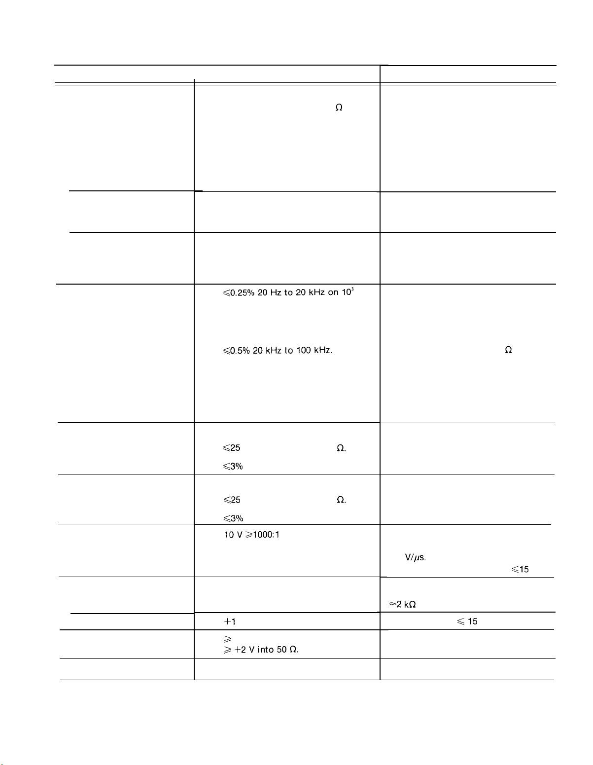
Table 1-1 (cont)
TM 9-6625-474-14&P-2
Characteristics
Amplitude Flatness
Sinewave
(10 kHz Sinewave Ref)
Squarewave
(10 kHz Squarewave Ref)
Triangle
(10 kHz Triangle Ref)
Sinewave Distortion
Performance Requirements
Measured with 0 dB ATTEN button
“IN” and output driving 50
(Front panel only.)
±0.1 dB 20 Hz to 20 kHz
±0.5 dB 20 kHz to 1 MHz
±1 dB 1 MHz to 2 MHz
Peak to peak amplitude within
±0.5 dB of squarewave reference
amplitude 20 Hz to 2 MHz.
Peak to peak amplitude within
±0.5 dB of triangle wave reference amplitude 20 Hz to 200 kHz.
Within 2 dB 200 kHz to 2 MHz.
range and below.
Cl
load.
Supplemental Information
Typically ±.5 dB .002 Hz to 20 Hz
Typically within ±.5 dB .002 Hz
to 20 Hz.
Typically within ±.5 dB .002 Hz
to 20 Hz.
20° to 30° C. Measured with
with average responding THD meter.
Measurement bandwidth limited to
approximately 300 kHz.
Q
Verified at 15 V p-p into 50
Must be on calibrated portion of
dial. VAR SYMM control off, Offset
control off.
load.
Squarewave Output
Risetime and Falltime
Aberrations (p-p)
Pulse Output
Risetime and Falltime
Aberrations (p-p)
VCF Input
Ext Trig/Gate Input
Impedance
Threshold Level
Trigger Output
Variable Phase Range
All harmonics at least 30 dB below
fundamental from 100 kHz to 2 MHz
Step ATTEN in 0 dB position.
<25 ns at 15 V p-p into 50
s30/o (Front panel only. )
Step ATTEN in 0 dB position.
<25 ns at 15 V p-p into 50
<30/o (Front panel only.)
+1
V ±20%.
>
+4 V into open circuit
>+2Vinto50f2.
At Ieast ±90°
Q
Q,
Trig output driving open circuit.
Positive going voltage increases
frequency. Maximum Slew Rate =
0.5
V/Ps.
VCF must not exceed
range limits, Maximum input
=2
kf2
Maximum input
Sine and Triangle only.
<15
V pk.
<15 V pk.
1-3
Page 12

TM 9-6625-474-14&P-2
Table 1-1 (cont)
Characteristics
Attenuators
Accuracy
Dial Accuracy
Triangle
Linearity
Time Symmetry
Characteristics
Power Consumption
Performance Requirements
±1 dB.
Within 3% of full scale 20 to 2.
Better than 1% 20 Hz to 200 kHz.
5% 200 kHz to 2 MHz (calibrated).
Table 1-2
MISCELLANEOUS
12 W or less. (plug-in only)
Supplemental Information
60 dB in 20 dB steps. >20 dB
additional attenuation with amplitude
control.
Verified at 20 kHz.
2 to .2 Uncal.
Greater than or equal to 99% 20 Hz to
200 kHz. 97% 200 kHz to 2 MHz (calibrated). Measured from 10% to
90% of waveform.
Description
Recommended Adjustment
Interval
Warm-up Time
Characteristics
Temperature
Operating
Non-operating
Humidity
Altitude
Operating
Non-operating
Vibration
1000 hours or 6 months, whichever occurs first.
20 minutes.
Table 1-3
ENVIRONMENTAL’
Description
Meets MlL-T-28800B, class 5.
0° C to +50° C
–55° C to +75° C
95% RH, 0° C to 30° C
Exceeds MlL-T-28800B, class 5.
75% RH to 40° C
45% RH to 50° C
Exceeds MIL-T-28800B, class 5.
4.6 Km (15,000 ft)
15 Km (50,000 ft)
0.38 mm (0.015") peak to peak,
5 Hz to 55 Hz, 75 minutes.
Exceeds MlL-T-28800B, class 5,
when installed in qualified
power modules.
b
1-4
Page 13

Table 1-3 (cont)
TM 9-6625-474-14&P-2
Characteristics
Shock
Bench Handling
Transportation
C
c
EMC
Electrical Discharge
a
With power module.
b
Refer to TM 500 power module specifications.
c
Without power module.
Description
30 G’s (1/2 sine), 11 ms duration, 3 shocks in each direction along 3 major axes, 18
Meets MlL-T-28800B, class 5,
when installed in qualified
power modules.
b
total shocks.
12 drops from 45°, 4“ or
Meets MlL-T-28800B, class 5.
equilibrium, whichever occurs
first.
Qualified under National Safe Transit Association Preshipment Test
Procedures 1A-B-1, and 1A-B-2.
Within limits of MIL-461A, and F.C.C. Regulations, Part 15, Subpart J,
Class A.
20 kV maximum charge applied to instrument case.
Table 1-4
Characteristics
Finish
Net Weight
Overall Dimensions
PHYSICAL CHARACTERISTICS
Description
Plastic/aluminum laminate front panel. Anodized aluminum chassis.
1.88 Ibs (.85 kg)
Height 5 in (126mm)
Width 2.6 in (67mm)
Length 11.9 in (303mm)
1-5/(1-6 blank)
Page 14
TM 9-6625-474-14&P-2
SECTION 2
OPERATING INSTRUCTIONS
INTRODUCTION
This section of the manual provides operating information required to obtain the most effective performance
from the FG 501A. Included are installation and removal
instructions, a functional description of the front panel
controls, and a general description of the operating
modes. Some basic applications of the instrument are also
briefly discussed.
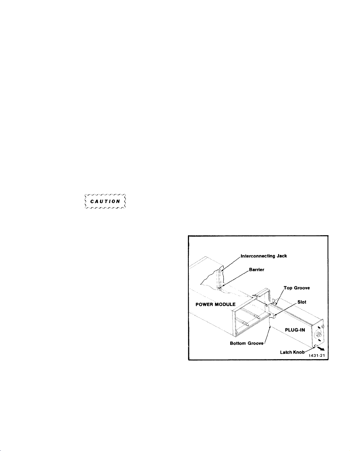
INSTALLATION AND REMOVAL
The FG 501A is calibrated and ready to use when
received. It operates in one compartment of any TM 500series power module. Refer to the power module instruc-
tion manual for line voltage requirements and power
module operation.
CAUTION
To prevent damage to the FG 501A, turn the power
module off before installation or removal of the
instrument from the mainframe. Do not use excessive force to install or remove.
showing: owner (with address) and the name of an
individual at your firm that can be contacted. Include
complete instrument serial number and a description of
the service required.
If the original package is not fit for use or not available,
repackage the instrument as follows:
Surround the instrument with polyethylene sheeting, or
other suitable material, to protect the exterior finish.
Obtain a carton of corrugated cardboard of adequate
strength and having inside dimensions no less than six
inches more than the instrument dimensions. Cushion
the instrument by tightly packing dunnage or urethane
foam between the carton and the instrument, on all
sides. Seal the carton with shipping tape or an industrial stapler.
The carton test strength for your instrument is 200
pounds.
Check to see that the plastic barriers on the interconnecting jack of the selected power module compartment match the cutouts in the FG 501 A circuit board edge
connector. If they do not match, do not insert the
instrument until the reason is found. When the units are
properly matched, align the FG 501A chassis with the
upper and lower guides of the selected compartment (see
Fig. 2-1). Insert the FG 501A into the compartment and
press firmly to seat the circuit board edge connector in the
power module interconnecting jack. Apply power to the
FG 501A by operating the power switch on the power
module.
To remove the FG 501A from the power module, pull
the release latch (located in the lower left corner) until the
interconnecting jack disengages. The FG 501A will now
slide straight out.
REPACKAGING FOR SHIPMENT
If the Tektronix instrument is to be shipped to a
Tektronix Service Center for service or repair, attach a tag
Fig. 2-1. Plug-in installation and removal.
2-1
Page 15
TM 9-6625-474-14&P-2
CONTROLS AND CONNECTORS
Although the FG 501A is calibrated and ready to use,
the functions and actions of the controls and connectors
should be reviewed before attempting to use it. All
controls necessary for operation of the instrument are
located on the front panel. A brief description of these
controls follows. Refer to Fig. 2-2.
2-2
Fig. 2-2. Controls and connectors.
Page 16
TM 9-6625-474-14&P-2
POWER - llluminated when power is applied to the
FG 501A.
FREQUENCY CONTROL AND FUNCTION
SELECTION
FREQUENCY Hz - Selects the frequency of the
output waveform
MULTIPLIER control.
FREQ + 10 - Illuminated when the variable symmetry function is activated.
FUNCTION BUTTONS - Select square, triangle,
and sine waveforms.
VAR SYMM - (push to enable) adjusts time-based
symmetry of the selected output waveform. Reduces
the frequency of the output waveform by a factor
= 10 and illuminates the FREQ + 10 indicator.
FREQUENCY VERNIER - For fine adjustment of
output frequency to at least 1 part in 10
MULTIPLIER - Selects the output frequency in eight
decade steps in conjunction with the FREQUENCY
Hz control.
in
conjunction with the
4
of full scale.
TRIGGER AND GATE CONTROLS
GATE - When pressed causes continuous output of
the selected waveform for the duration of the gating
pulse.
SLOPE - Button selects, in TRIG mode, the slope of
the input signal which will trigger the selected
output waveform. In GATE mode, whether output
gating will occur when the level of the input signal is
above or below the threshold level of +1 V.
TRIG/GATE lN - Bnc connector used to apply the
external trigger or gating signal.
VCF lNPUT - Bnc connector for applying an exter-
nal voltage for controlling the output frequency of
the generator.
TRIGGER OUTPUT - Bnc connector which outputs
one positive pulse for each cycle of the selected
output waveform.
OUTPUT CONTROLS
ATTENUATOR BUTTONS - Attenuate the ampli-
tude of the selected output waveform in 20 dB steps
to a maximum of 60 dB when pressed.
AMPL - Varies the amplitude of the selected output
waveform, between steps of the attenuator buttons.
VAR
0
relative to input trigger or gate waveform.
FREE RUN - When pressed causes continuous
waveform output.
TRIG - When pressed causes output of one cycle of
selected waveform for each trigger pulse applied to
the TRIG/GATE IN connector.
- Selects phase lead or lag, up to ±90°,
OFFSET - Pull and turn control, concentric with the
AMPL control, provides up to ±13 V dc offset of the
output waveform.
OUTPUT - Bnc connector for output of the selected
waveform.
RELEASE LATCH - Pull to disengage the FG 501A
from the power module.
2-3
Page 17

TM 9-6625-474-14&P-2
OPERATING CONSIDERATIONS
OUTPUT CONNECTIONS
The output of the FG 501A is designed to operate as a
50
fl
voltage source working into a 50 Q load. At higher
frequencies, an unterminated or improperly terminated
output will cause aberrations on the output waveform.
Loads less than 50
Excessive distortion or aberrations, due to improper
termination, are less noticeable at the lower frequencies
(especially with sine and square waveforms). To ensure
waveform purity, observe the following precautions:
1. Use good quality 50
tors.
2. Make all connections tight and as short as possible.
3. Use good quality attenuators if it is necessary to
reduce waveform amplitude applied to sensitive circuits.
4. Use terminations orimpedance matching devices to
avoid reflections when using long cables (6 feet or more).
~
will reduce the waveform amplitude.
Q
coaxial cables and connec-
capacitance) of the vertical input of an oscilloscope,
Q
connect the transmission line to a 50
termination, and then to the oscilloscope input. The
attenuator isolates the input capacitance of the device,
and the FG 501A is properly terminated.
attenuator, 50
FIRST TIME OPERATION
The Controls and Connectors pages give a description
of the front panel controls and connectors, The waveform
selection and frequency determining control sareoutlined
in blue, the trigger function controls and inputs are
outlined in green, and the output controls are outlined in
black.
The following exercise will familiarize the operator with
most functions of the FG 501A.
NOTE
If any discrepancies are encountered during the
exercise, refer the condition to qualified service
personnel,
Q
5. Ensure that attenuators, terminations, etc. have
adequate power handling capabilities for the output
waveform.
If there is a dc voltage across the output load, use a
coupling capacitor in series with the load. The time
constant of the coupling capacitor and load must be long
enough to maintain pulse flatness.
RISETIME AND FALLTIME
If the FG 501A is used to measure the rise or falltime of
a device, the riestime characteristics of associated equipment should be considered. If the risetime of the device
under test is at least 10 times greater than the combined
risetimes of the FG 501A and associated equipment, the
error introduced will not exceed
ignored. When the rise or falltime of the test device is less
than 10 times as long as the combined risetimes of the
testing system, the actual risetime of the system must be
calculated. The risetime of the device under test can be
determined once the risetime of the system is known.
1%, and generally can be
IMPEDANCE MATCHING
If the FG 501A is driving a high impedance such as the
1
MQ
input impedance (paralleled by a stated
Preset the controls as follows:
Blue section:
FREQUENCY Hz
MULTIPLIER
FREQUENCY VERNIER
WAVEFORM—SINE
VAR SYMM
Green section:
FREE RUN
Black section:
ATTENUATOR
AMPL (variable)
OFFSET
Connect a 50
the vertical input of an oscilloscope. Set the oscilloscope
controls to:
Vertical
Horizontal (Time Base)
The oscilloscope should display 1 complete cycle per
division of the sine waveform ( approximately 10 cycles
across the graticule),
Q
bnc coaxial cable terminated in 50 f2to
10
10
Fully CW
in
off
in
-20 dB
Centered
off
1 V/Div DC Coupled
1 ms/Div
2-4
Page 18

TM 9-6625-474-14&P-2
1. Alternately press the square, triangle and sine
buttons and observe the different waveshapes. Return to
the preset condition.
2. Alternately press the four attenuator buttons and
rotate the AMPL (variable) control to verify that the
waveform amplitude changes. Return these controls to the
preset condition.
3. Pull the OFFSET knob out and rotate it. Notice the
change in dc level of the displayed waveform. Return the
OFFSET knob to the in position.
OPERATING MODES
FREE-RUNNING OUTPUT
The following procedure will provide a free-running
output with variable frequency and amplitude.
1. Select the desired waveform.
4. Push the VAR SYMM button to release it to the out
position. Observe that the FREQ
luminated and only one cycle of the output waveform is
displayed. Rotate the VAR SYMM control through its
range and notice the change in shape of the square,
triangle, and sine waveforms (with the appropriate buttons
pushed in). Return the controls to the preset condition.
5. Rotate the FREQUENCY control and the
MULTIPLIER switch while observing the change in frequency of the displayed
to the preset condition,
If more than one cycle of the output waveform is
desired, push the GATE button. The output will now be
continuous for the duration of the gating waveform. The
number of cycles per burst can be approximated by
dividing the gating signal duration by the period of
FG 501A output frequency,
waveform, Return these controls
+
10 indicator is il-
2. Set the AMPL control fully counterclockwise. Check
that the VAR SYMM and OFFSET controls are in the off
(in) position.
3. Select the desired frequency with the FREQUENCY
Hz dial and MULTIPLIER switch. Frequency equals dial
setting times multiplier setting.
4. Connect the load to the FG 501A output connector
and adjust the AMPL control for the desired output
amplitude.
TRIGGERED OR GATED (BURST)
OPERATION
With the FG 501A set for free-running operation, as
described in previous paragraphs, apply the triggering or
gating signal to the TRIG/GATE IN connector.
If only one cycle of the output waveform per trigger is
desired, push the TRIG button and select + or – slope.
One output cycle will now be generated for each input
trigger cycle.
In triggered or gated operation the PHASE control
varies the start of the output waveform by ±90°. This
phase change is measured from the 0 V, 0° point on the
output waveform.
VOLTAGE CONTROLLED FREQUENCY
(VCF) OPERATION
The output frequency of any selected waveform can be
swept within a range of 1000:1 by applying an external
voltage to the VCF INPUT connector. The polarity of the
VCF input signal determines which direction the output
frequency sweeps from the selected frequency, A positive
(+) going signal increases the frequency while a negative
(–) going signal decreases the frequency. The amplitude
and polarity of the input voltage can be selected within a
range of ±10 V depending on the FREQUENCY Hz dial
setting.
The maximum swept frequency range of 1000:1 encom-
passes the uncalibrated portion of the FREQUENCY Hz
dial (<.2 to 2). To ensure that the frequency does sweep at
least a range of 1000:1, it is recommended that the
FREQUENCY Hz dial be set at .2 and a 0 to +10 V signal be
applied to the VCF INPUT connector. It may be necessary
2-5
Page 19
TM 9-6625-474-14&P-2
to vary the FREQUENCY VERNIER control to obtain the
full 1000:1 swept range or the lowest swept frequency
desired.
Since the VCF input amplitude is a linear relationship,
the frequency output range can be determined from the pulse is generated for each negative cycle of the output
VCF input amplitude.
A +4 V square wave is available from the TRIG
OUTPUT connector. The frequency of the trigger output
is determined by the frequency of the selected output
waveform. One trigger pulse is generated for each positive
cycle of the output signal except when square waves are
selected. When generating square waves, one trigger
signal. Trigger output impedance is
TRIGGER OUTPUT
50’(2.
BASIC WAVEFORM CAPABILITIES
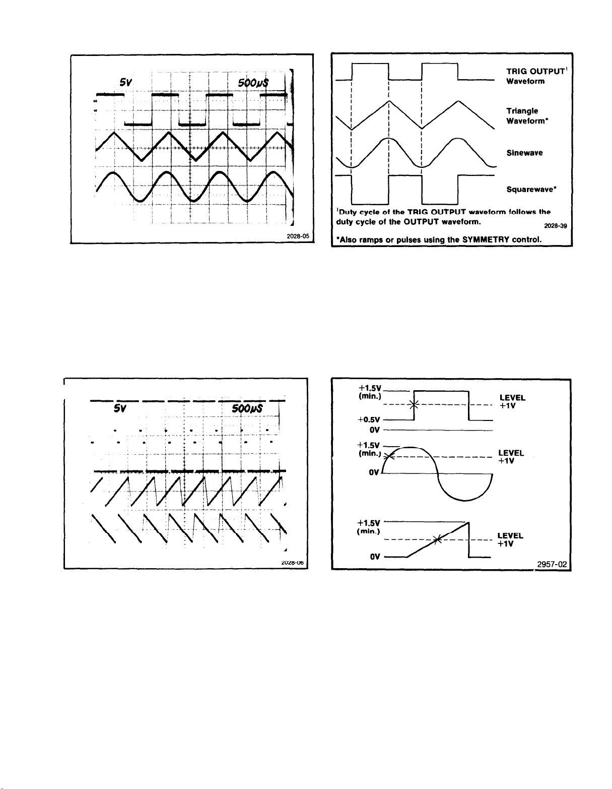
The following photographs illustrate the basic waveform capabilities of the FG 501A.
2-6
Fig. 2-3. Swept Frequency range with 10 V signals applied to VCF IN connector.
Page 20
TM 9-6625-474-14&P-2
Fig. 2-4. BASIC FUNCTIONS. Square, triangle, and sine
waveforms selected by front panel pushbuttons.
Fig. 2-6. Phase relationships between OUTPUT waveforms and
the TRIG OUT waveform.
Fig. 2-5. RAMPS AND PULSES. These are obtained from the Fig. 2-7. Trigger Signal amplitude requirements and triggering
basic waveforms by using the SYMMETRY control.
points.
2-7
Page 21

TM 9-6625-474-14&P-2
Fig. 2-8. GATED OPERATION. The top three traces are various
output waveforms and the bottom trace is the gating waveform
applied to the trigger INPUT connector with the GATE
pushbutton pressed in. Note the additional cycle completed after
the waveforms are gated off.
Fig. 2-10. PHASE CONTROL OPERATION. This photograph
illustrates PHASE control usage in the triggered mode. The five
super-imposed traces illustrate the effect of the phase control.
This control provides ±90° of shift. The bottom trace is the
triggering waveform.
Fig. 2-9. TRIGGERED OPERATION. The top three traces are the
various out put traces selected. The bottom trace is the triggering
waveform applied to the trigger INPUT connector with the TRIG
mode selected. Note that only one cycle of the output waveforms
is completed.
2-8
Page 22

APPLICATIONS
TM 9-6625-474-14&P-2
RESPONSE ANALYSIS
The FG 501A is particularly suited for determining
resIponse characteristics of circuits or systems. This
application utilizes the VCF input of the FG 501 Ato sweep
the generator over a range of frequencies. Refer to the
Voltage Controlled Frequency (VCF) Operation discussion under Operating Modes for additional information.
1. Connect the equipment as shown in Fig. 2-11.
5. Observe the response characteristics on the
monitoring oscilloscope.
The frequency at which a displayed response
characteristic occurs can be determined by first removing
the VCF input waveform, then manually adjusting the
FREQUENCY Hz dial to again obtain the particular
characteristic observed in the swept display and reading
that frequency on the FREQUENCY Hz dial.
TONE-BURST GENERATION OR
2. Set the MULTIPLIER selector and FREQUENCY Hz
dial for the desired upper or lower frequency limit
(depending on the direction you wish to sweep).
The FG 501A can be used as atone-burst generator or
frequency multiplier for checking tone-controlled
3. Apply the desired waveform to the VCF INPUT
connector. (A positive-going waveform will increase the
frequency while a negative-going waveform will decrease
it. )
4. Adjust the amplitude of the VCF input waveform for
the desired output frequency range. obtaining a tone-burst or frequency multiplied output
devices. This application utilizes a ramp generator, such
as the TEKTRONIX RG 501, as a VCF signal source and a
pulse generator, such as the TEKTRONIX PG 501, as a
gating signal source.
The following procedure describes a technique for
STEPPED FREQUENCY
MULTIPLICATION
Fig. 2-11. Analyzing circuit or system response.
2-9
Page 23
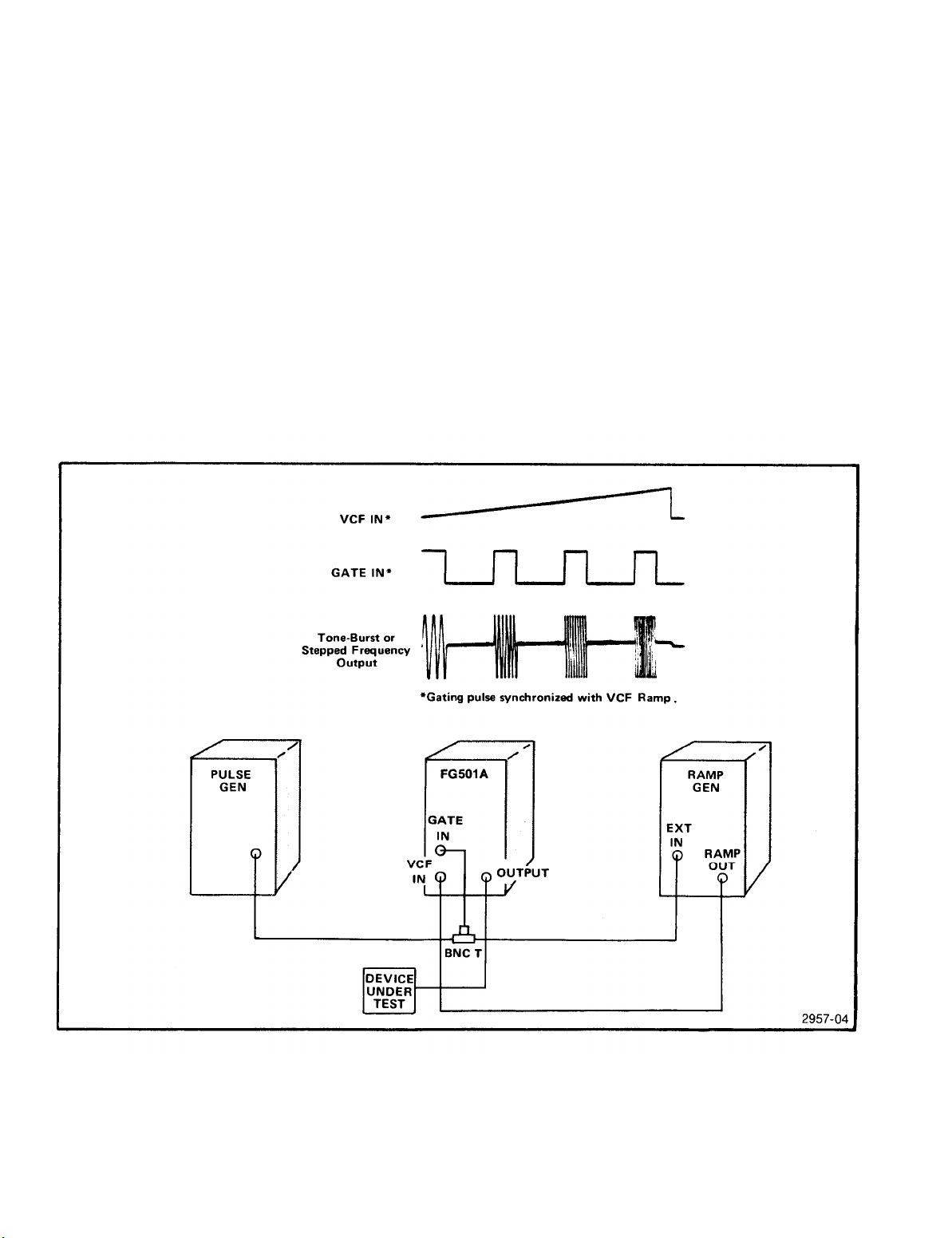
TM 9-6625-474-14&P-2
from the FG 501A. Refer to the Gated (burst) Output and
Variable Phase and the Voltage-controlled Frequency
(VCF) Output discussions under Operation for additional
information.
1. Connect the equipment as shown in Fig. 2-12.
2. Push the GATE button in and set the PHASE control
to the desired phase.
3. Set the ramp generator for the desired ramp dura-
tion and polarity.
4. Adjust the pulse generator period for the desired
number of bursts within the selected ramp duration. input waveforms, i.e., triangle, sine, square, etc.
Adjust the pulse generator duration for the desired burst
width.
5. Select the sweep frequency range by adjusting the
FREQUENCY Hz dial for one end of the sweep range
(upper or lower limit depending on the polarity of the
ramp). Then, adjust the ramp generator amplitude for the
other swept frequency limit.
Various other tone-burst or frequency multiplied
characteristics can be obtained by using different gating
2-10
Fig. 2-12. Tone-burst generation or stepped frequency multiplication.
Page 24

TM 9-6625-474-14&P-2
SECTION 3
THEORY OF OPERATION
INTRODUCTION
This section of the manual contains a description of the
electrical circuits in the FG 501A. Refer to the block throughout this section refer to the schematic diagram on
diagram and schematic diagrams on the fold out pages in which the circuit being discussed is located.
the back of the manual to aid in understanding this
LOOP
FREQUENCY CONTROL AND SUMMING
AMPLIFIER
The voltage developed across the frequency control
divider string, R1429, R1321, R500 and R510, is applied to
pin 5 of operational amplifier U1540B. This voltage is
buffered by the amplifier and. a current is developed
through R1551. This current is applied top in 2 of summing
amplifier U1540A where it is summed with any currents
developed by a voltage applied tothe VCF inputs. The VCF
inputs are J510 (front panel) through R1553, and pin 21B
(rear interface) through R1103. These summed currents
are buffered by Q1445 and flow through R1543. The
voltage developed across R1543 is proportional to the
frequency.
CURRENT SOURCES AND SWITCH
The voltage developed across R1543 is buffered by
U1440 and Q1541 which form the negative current source
for the main Ioop timing circuitry. This same voltage is also
buffered by U1540C and Q1543 which form a current
source identical to U1440 and Q1541. The output current
from Q1543 flows through Q1527, Q1525, and Q1421,
which form a current mirror that inverts this current to
provide the positive current source for the main loop
timing circuitry. The current through R1521 is the timing
capacitor charging current; the current through R1536 is
the discharging current. The Top Dial Symmetry Cal,
R1421, adjusts the balance between these two currents so
they are equal in magnitude.
description. Diamond enclosed numbers appearing
@
positive and negative current sources. In this manner the
symmetry of the waveform generated by the loop is varied.
These currents are switched into the junction of CR1531
and CR1533 where they alternately charge and discharge
the timing capacitor, producing a triangle waveform, The
current switch is formed by Q1531, CR1531, Q1433 and
CR1533.
TIMING CAPACITORS AND
@
@
5
(C1631)
0
down to
CAPACITANCE MULTIPLIER
The timing capacitors provide for triangle generation in
the five fastest MULTIPLIER ranges. They are switched
into and out of the circuit in decade stepsfrom 10
down to 10
For the four lower MULTIPLIER ranges, 10
10-’,
C1741 is switched into the feedback loop of U1930
forming an integrator. Current from the current switch is
applied to operational amplifier U1940. A voltage is
developed at the output of this amplifier that is propor-
tional to the applied current times the value of R1941
(1
kfl).
resistors, to the input of U1930. These resistors, R1831,
R1841, R1842, and R1843, are switched into and out of the
circuit in decade steps with the MULTIPLIER switch
S1731. This arrangement provides very large values of
effective capacitance. The output of U1930 is now the
triangle that is applied to the buffer stage.
1
(C1741).
This voltage is applied, across one of four
TRIANGLE BUFFER
In the normal mode of operation (fixed symmetry) R520
and R540 are in the emitter circuit of Q1541 and Q1543. In
this condition, equal amounts of current will flow in both
the positive and negative current sources. When S500,
VAR SYMM, is activated, R530 is switched into the current
source emitter circuits. As R530 is varied from one end to
the other, unequal amounts of current flow through the
The voltage developed by the timing capacitor or
multiplier (U1930) is applied to the triangle buffer. Q1725
and Q1723 form the differential input stage of this circuit.
Q1821 serves as a constant current source for the input
differential pair. Q1721 and Q1712 complete the feedback
for the amplifier such that the voltage at the emitter of
Q1712 is equal to the voltage at the Gate of Q1725.
3-1
Page 25

TM 9-6625-474-14&P-2
Loop delay compensation is provided by a network
comprised of R1712, R1812, C1712, and C1714. The
buffered timing capacitor voltage is applied through this
network to the level comparators.
(~)
low and pin 8
to the current switch, Q1531 will be turned off and Q1433
turned on. This allows the timing capacitor to charge in the
positive direction.
to go high. Taking this high at pin 8 back
LEVEL COMPARATORS
The level comparators detect upper and lower
threshold levels. U1700A is the upper level detector and
U1700B the lower. The reference level for these comparators is supplied by U1400B and C. As the threshold
levels are detected, the respective comparator triggers
U1600B.
REFERENCE VOLTAGES
The reference voltage supplies are composed of
U1400B (–) and U1400C (+) and associated components.
The upper (positive) level threshold voltage is established
by adjusting R1412. This resistor is in a voltage divider
string from zener diode VR1413. The voltage developed
across R1412 is buffered by U1400C and set to approximately +400 mV at the output. This voltage is applied
to pin 5 of U1700A as the upper threshold level reference.
This same voltage is also applied to pin 9 of inverter
U1400B. R1511 is used to adjust the gain of this stage so
that the output is nominally –400 mV. This voltage is
applied to pin 13 of U1700B as the lower threshold level
reference.
LOOP LOGIC
When a rising voltage at pin 6 of U1700A passes
through the threshold level set at pin 5, the output (pin 8)
goes low pulling pin 10 of U1600Blow. This action sets the
flip-flop causing pin 9 (Q) to go high and pin 8 (Q) to go
low. Pin 8 of U1600B is tied back, through R1403, to the
junction of CR1431 and VR1532. VR1532 serves as a level
shifter to change the TTL output gate to the correct level to
drive the current switch (Q1531, CR1531, Q1433,
CR1533).
As the voltage at the junction of R1532 and R1534
drops, it pulls the bases of Q1531 and Q1433 low. Q1531 is
turned on and Q1433 is turned off. Any current from the
positive current source, through R1521, now flows
through Q1531 and is shunted to the –15 V supply. With
Q1433 turned off, any current flow through the negative
current source must come from the positively charged
timing capacitor through CR1533.
The falling voltage on the timing capacitor is buffered
through the triangle buffer and applied to the level
comparators U1700A and U1700B. As the voltage at pin 12
of U1700B falls through the threshold level set at pin 13,
the output (pin 1) goes low pulling pin 13 of U1600Blow.
This action resets the flip-flop causing pin 9
(Q) tonowgo
The action just described generates one entire cycle of
a triangle wave.
TRIGGER GENERATOR
The square wave output at pin 8
drives the trigger output amplifier. This circuit is composed of emitter follower Q1431 and associated components. Q1440, in conjunction with R1440, serves as
output short circuit protection. The output of this circuit
(at J2043) is a square wave 180° out of phase with the main
loop signal. The output amplitude is greater than +4 V into
an open circuit, and at least +2 V into a 50
(~)
of U1600B also
f2
load.
SQUARE WAVE GENERATOR
The output at pin 9 (Q) of U1600B is a square wave, but
180° out of phase with that at pin 8. This signal is used to
drive the square wave generator composed of differential
pair Q1801, Q1901, and associated components. The base
of Q1901 is held at a constant voltage by divider network
R1815 and R1818. R1728 and R1816 form a constant
current source for the differential pair. The square wave
from U1600B alternately switches this constant current to
ground through Q1801 or through R1819 and Q1901. In
this manner, a square wave voltage is developed with dc
levels sufficient to drive the output amplifier for the square
wave function.
PHASE CLAMP THRESHOLD DETECTOR
The output of the triangle buffer, in addition to possibly
being fed to the Output Amplifier through S1901B, is
connected to the base of Q1711. Q1711 and Q1611 form a
differential amplifier. Q1621 and associated components
provide a constant current source for the differential pair.
This amplifier senses the level of the triangle waveform
and compares it to the output voltage of U1400A. The
output voltage of U1400A is determined by the setting of
the VAR 0 control, R550. The voltage range of R550 is
established by reference voltage supplies U1400B (–) and
U1400C (+). These are the same reference voltages
supplied to the Level Comparators. This arrangement
permits comparison of the triangle voltage with the
maximum possible positive and negative levels, and all
levels between.
When the triangle voltage exceeds the reference
voltage set by the VAR 0 control, Q1711 turns off. Any
current flowing through Q1621 now flows through Q1611.
3-2
Page 26

TM 9-6625-474-14&P-2
CURRENT AMPLIFIER
Current flowing through Q1611 also flows through
R1622 and is amplified by Q1521. Temperature compensation for this amplifier is provided by CR1621. Differential
pair Q1511 and Q1523 serve as a current switch. With
Q1511 turned off, any current amplified by Q1521 passes
through Q1523 to the junction of CR1531 and CR1533.
When the timing capacitor voltage rises to the threshold
TRIG/GATE AMP AND SINE SHAPER
TRIG/GATE AMP AND LOGIC
The input trigger amplifier consists of an emitter
coupled differential pair (Q1320 and Q1322), current
amplifier Q1324, and the required logic circuitry to control
the operation of the main loop phase clamp. Input circuit
protection is provided by R1203, R1204, CR1220 and
CR1221. Triggering signals are applied either through
front panel connector J520 or interface connections on
the rear edge of the Main circuit board.
The differential pair, Q1320-Q1322, responds to the
input signal when the voltage rises above (+ SLOPE) the
reference voltage at the base of Q1320. This reference
voltage is established by divider network R1312 and
R1314, The position of S1400D, SLOPE switch, determines whether a positive or negative going input will
cause the amplifier Q1324 to conduct. When the threshold
level is exceeded and conduction starts, current flow
through the circuit causes a voltage to be developed
across R1322. This voltage is applied to the base of Q1324.
The output at the collector of Q1324 is a TTL compatible
waveform to drive the logic circuit, U1310. CR1320
provides temperature compensation for Q1324.
level set by the VAR 0 control, R550, it is clamped. Q1523
now draws exactly the amount of current that the positive
current source supplies. Because the square wave at pin 5
(Q) of U1600A drives the base of Q1511, the clamping
action only happens during the positive edge of the
triangle wave. On the negative transition, Q1523 is shut
off, and Q1511 is on. In this manner, the timing capacitor
voltage can be clamped at any desired positive level.
@
as long as this condition exists. As soon as the level at the
input connector drops below the threshold, the output
voltage of U1310A rises. This high level causes the
generator to again stop running when the phase clamp
reaches its threshold level at the end of the last complete
cycle.
In the FREE RUN mode, S1400A is positioned such that
pin 4 of U1600A is held low. The generator now outputs
continuous waveforms.
SINE SHAPER
The Sine Shaper is composed of three separate circuit
functions: a Transconductance Amplifier, the Shaper
Circuitry, and an Output Buffer.
Transconductance Amplifier. Emitter coupled tran-
sistors Q1210 and Q1212 along with current source Q1200
form the Transconductance Amplifier. The amplifier con-
verts the triangle voltage at the base of Q1212 to a
differential current. This current flows through two sets of
diode wired transistors, U1120C, U1120D, U1220C, and
U1220D, to the input of the shaper.
Three modes of operation are selectable with S1400;
Triggered, Gated, and Free Running.
In the TRIG mode, S1400A and S1400C are positioned
such that the output, pin 6, of U1310B is connected to pin
4, set input, of U1600A. In this mode, a very narrow,
negative going voltage pulse is developed by U1310B each
time the input waveform passes through the trigger
threshold. This low sets U1600A, which deactivates the
phase clamp until the triangle generator again starts in the
positive direction, and allows the generator to complete
one full cycle.
In the GATE mode, S1400A and S1400C are positioned
such that the output, pin 3, of U1310A is connected to pin
4, set input, of U1600A. In this mode, a low level is
produced whenever the input waveform exceeds the
threshold if + SLOPE is selected. The generator free runs
Shaper. The active portion of the Shaper is formed by
two sets of emitter coupled transistors U1220A, U1220B,
U1120A and U1120B. These devices have their inputs
wired in series and their outputs cross coupled. U1120E
and U1220E are current sources for these devices. The
circuit operates by generating a power series approximation to the sine function. The devices in U1120 generate
the first order term while those in U1220 generate the
second order term in the approximation.
Output Buffer. The Output Buffer is an operational
amplifier that converts the differential current from Q1010
and U1020D to a single ended voltage that is applied,
through the function switch, to the output amplifier.
U1020E is a current source for the emitter coupled
differential input pair U1020A and U1020B. Q1012 serves
as a current mirror for U1020A and as an active load for
U1020B. U1020C is the output emitter follower and R1020
is the feedback resistor.
3-3
Page 27

TM 9-6625-474-14&P-2
OUTPUT AMPLIFIER & ATTENUATORS
The output amplifier is basically a noninverting
operational amplifier whose plus input is the base of
Q2101 and minus input is the base of Q2113.
The three basic waveforms are selected by S1901 and
applied across R560B and R2335 to the input stage of the
amplifier. R560B varies the amplitude of the selected
waveform. The feedback network consists of R2011 and
R2012, connected from the output to the minus input of
the amplifier. C2011 provides high frequency compensation for the feedback, and is used to adjust the squarewave
front corner. The input pair, Q2101 and Q2113, amplify the
difference between the input waveform and the fedback
waveform.
An offset current is also summed with the feedback
signal at the base of Q2113 when S510A is closed. This
allows R560A to control the dc offset of the output signal.
POWER SUPPLY
The FG 501A receives its power from the power module
via interface connections on the rear edge of the Main
circuit board. The power module supplies plus (+) and
minus (–) 33.5 Vdc (unregulated) from which the following regulated voltages are generated.
+20 V SUPPLY
The +33.5 V from the power module is filtered and
applied to voltage regulator U1210 (pins 11 and 12). This
regulator contains its own reference, operational
amplifier, and current Iimiting elements. The output of the
regulator is applied to Q1231 which serves as a driver the
the series pass transistor located in the power module.
The +20 V output is applied across voltage divider R1201,
R1301, and R1315. The output level of the supply is set by
R1301 (+15 V Adj) which compares the supply output to
the internal reference level of the regulator. This supply is
current limited through the action of R1121 and the
current limiting element in the regulator. When excessive
amounts of current are drawn from the supply, the voltage
developed across R1121 turns on the current limiting
element in the regulator (U1210). This action reduces the
base drive, through Q1231, to the series pass transistor
causing the supply to reduce output, This supply is the
reference for other supplies in the FG 501A.
@
The output of Q2101 is applied directly to Q2111 which
is cascoded with Q2011. The output of Q2113 passes
through an inverting amplifier, Q2211, before passing to
Q2213 cascoded with Q2311. CR2111 provides temperature compensation for Q2211. The two cascodes form
drivers for the amplifier output stage.
The output stage consists of Q2013 and Q2123 in
parallel with Q2121 for amplification of positive going
signals. Q2321 and Q2323 in parallel with Q2325 form the
amplifier for negative going signals. The output is taken at
the junction of R2026 and R2228. The 50
impedance is determined by parallel 100
R2033 and R2131. C2121 in this network provides high
frequency compensation for the output impedance, The
attenuator circuit is a constant impedance resistive divider
network, switch selectable in 20 dB steps.
f2
output
Q
resistors
@
+20 V supply. Since this supply is sourced from the +20 V,
it is inherently current limited by the +20 V supply.
+5 V SUPPLY
The +5 V supply consists of U1230C and Q1331.
U1230C serves as an error amplifier which compares the
+5 V output to a +5 V reference developed by divider
network R1231, R1232 and R1233 from the +20 V supply.
Since this supply is sourced from the +15 V and referenced
to the +20 V supply, it is inherently current limited under
the same conditions that limit those supplies.
–20 V SUPPLY
The –20 V supply is derived from –33.5 V supplied by
the power module. The output of operational amplifier
U1230A is applied, through Q1245, to the base of Q1241,
which serves as a driver for the series pass transistor
located in the power module. This supply is also referenced to the +20 V. The supply is current limited through the
action of R1141 and Q1243. When excessive amounts of
current are drawn through R1141, a voltage sufficient to
turn Q1243 on develops across R1141. This action reduces
the base drive to the series pass transistor causing the
supply to reduce output.
–15 V SUPPLY
+15 V SUPPLY
The +15 V supply consists of U1230D and Q1221.
U1230D serves as an error amplifier which compares the
F15 Voutput of the supply to a +15 Preference developed
by divider network R1231, R1232 and R1233 from the
3-4
The –15 V supply consists of operational amplifier
(U1230B) and a series pass feedback regulator (Q1345),
The output of the supply is fed back through divider
network R1247, R1341, and R1245. The output level is
adjusted by R1341. Because this supply is sourced from
the –20 V supply, it is current limited by the –20 V supply.
Page 28

SECTION 4
CALIBRATION
PERFORMANCE CHECK
TM 9-6625-474-14&P-2
INTRODUCTION
This procedure checks the Electrical Performance
Requirements as listed in the Specification section in this
manual. Perform the internal adjustment procedure if the
instrument fails to meet these checks. If recalibration does
not correct the discrepancy, circuit troubleshooting is
indicated. Also, use this procedure to determine acceptability of performance in an incoming inspection facility, The test equipment, or equivalent, listed in Table 4-1 is
For convenience, many steps in this procedure check the
performance of this instrument at only one value in the
Table 4-1
TEST EQUIPMENT REQUIRED
Minimum Application
Item Description Specifications
1
Power Module Five compartments or more.
2
Oscilloscope System
3
Differential Comparator Minimum Vertical deflection
Amplifier
Minimum Vertical deflection
Sweep Rate .5
factor .1 V/div
PS.
specified performance range. Any value within the
specified range, within appropriate limits, may be substituted.
TEST EQUIPMENT REQUIRED
suggested to perform the performance check and the
adjust ment procedure.
Perf Adj
Check
X X
X X
X X
Proc
TEKTRONIX TM 515 or
TM 506
TEKTRONIX 7704/4/
7A16A/7B50
TEKTRONIX 7A13
Example
4
Sampling System
5
Spectrum Analyzer
Distortion Analyzer Frequency range from 20 Hz
6
to at least 300 kHz. Distortion
resolution <0.25%
7
Frequency Counter Frequency range 0.002 Hz
to above 2 MHz. Accuracy within
one part in 10
8
Digital Multi meter
Pulse Generator 0 to 2 V square wave
9
10
Power Supply
Range to ±30 V 5 1/2 digits
Accuracy 0.1%.
output into 50
Period 2
0 to 10 V range
Accuracy ±10%
,US;
Duration .1
4
±1 count.
f2
load.
ps
X
X
X
X X
X
X
X
Tektronix 7704/7S11/
7T11/S-1
TEKTRONIX 7L12
X
TEKTRONIX AA 501
X
TEKTRONIX DC 504
TEKTRONIX DM 501
TEKTRONIX PG 501
TEKTRONIX PS 501-1
4-1
Page 29

TM 9-6625-474-14&P-2
Minimum
Item Description Specifications
11
Flexible Extender Compatible with TM 500-
Series Power Modules
Black
12
Cable
Meter Lead
Table 4-1 (cont)
Application
Perf Adj
Check
X
Proc
X
X
Example
Tektronix Part No,
067-0645-02
Tektronix Part No.
012-0462-00
13
Meter Lead
14
Oscilloscope Probe
15
Coaxial Cable 50 !2 BNC Connectors
16
Termination 50 Cl BNC Connectors
X10 Attenuator
17
X5 Attenuator
18
19
Adapter BNC Female to Dual Banana
Red
X10 10
50
Cl
(20 dB) BNC
50
~
(14 dB) BNC
Mf2
1. Check Frequency Range
a. Connect the OUTPUT connector of the FG 501 to the
counter input.
b. Press the FEE RUN and 0 dB pushbuttons.
X X
Tektronix Part No.
012-0462-01
X X
Tektronix Part No.
010-6053-13
X X
Tektronix Part No.
012-0057-01
X
X
Tektronix Part No.
011-0049-01
X
Tektronix Part No.
011-0059-02
X
Tektronix Part No.
011-0060-02
X X
Tektronix Part No.
103-0090-00
i. Adjust the VAR SYMM control for a 50% duty cycle
pulse waveform.
j. CHECK - that the counter reads from 180 kHz to
220 kHz.
c. Press either the
W , ~ or N pushbuttons.
d. Make certain the VAR SYMM and OFFSET controls
are off.
e. Set the FREQUENCY Hz dial to 20 and the
MULTIPLIER control to the 10
5
position.
f. Adjust the AMPLITUDE control for a stable counter
display.
g. CHECK - that the counter reads
>2
MHz.
h. Activate the VAR SYMM control.
4-2
k. Change the MULTPLIER to 10-3.
l. CHECK - for an output frequency of between 0.0019
Hz and 0.0021 Hz.
m
Disable the VAR SYMM control.
n.
Change the FREQUENCY Hz dial to 2.
CHECK - that the FREQUENCY Hz dial can be ad-
o.
justed to obtain 0.0002 Hz.
p. Disconnect the counter for the next step
Page 30

2. Check Variable Symmetry Duty Cycle
Press the FREE RUN, 0 dB and ~ pushbuttons.
a.
d. Adjust the VAR
dmm.
TM 9-6625-474-14&P-2
0
control for a 0 V reading on the
Release the VAR SYMM pushbutton.
b.
Connect the OUTPUT connector through a 50
c.
coaxial cable to the oscilloscope vertical input:
d. Adjust the START, MULTIPLIER, AMPLITUDE, and
oscilloscope controls to display a squarewave that occupys exactly 10 major divisions for one cycle.
e. Rotate the VAR SYMM control from fully cw to fully
CCW.
f. CHECK - that the oscilloscope display varies each
squarewave half cycle from
<1/2
major division to >9.5
major divisions.
g. Leave these connections for the next step.
3.
Check Output Amplitude
a. Using the same setup as in the previous step, turn
the AMPLITUDE control fully
CW.
e. Pull and turn the OFFSET control fully cw to fully
CCW.
Q
f. CHECK - that the dmm reads
propriate stops for the OFFSET control.
g. Remove the coaxial cable from the dmm and insert a
50
f)
termination.
h. CHECK - that the dmm reads at least ±6.5 V at the
appropriate stops of the OFFSET control.
i. Remove the connections from the dmm for the next
step.
5. Check Amplitude Flatness
a. Press the FREE RUN, 0 dB and \ pushbuttons.
b. Make certain the OFFSET is off.
>+13
V at the ap-
b. CHECK - that the waveform on the oscilloscope
display is
>30 V peak to peak.
c. Remove the coaxial cable from the oscilloscope
vertical input and connect a 50
f2termination in series with
the cable.
d. CHECK - that the oscilloscope display is
peak to peak.
e. Disconnect the 50
f)
cable and remove the 50
termination from the oscilloscope for the next step.
4.
Check Offset Range
Press the TRIG 0 dB, and N pushbuttons.
a.
Make certain the VAR SYMM pushbutton is in.
b.
Connect a dmm set to read ±15 V to the output
c.
connector.
>15 V
c. Set the FREQUENCY Hz dial to 10 and the
MULTIPLIER to 10
d. Connect the OUTPUT connector through a 50
3
.
Q
cable and 50 Cl termination to the vertical input of the
differential oscilloscope plug-in.
e. Adjust the AMPLITUDE control and the gain of the
vertial amplifier for an 8 major division peak to peak
display.
f)
f. Increase the vertical amplifier gain by a factor of 10.
g. Adjust the vertical amplifier plug-in offset voltage so
that the waveform peaks are on the oscilloscope graticule
center line.
h. Change the output to any frequency from 20 Hz to
20 kHz.
i. CHECK - that the display is within 0.46 major
divisions from graticule center.
4-3
Page 31

TM 9-6625-474-14&P-2
j. Change the output to any frequency from 20 kHz to
1 MHz.
k. CHECK - that the display is within 2.37 major
divisions from graticule center.
l. Decrease the vertical gain of the oscilloscope by a
factor of 10 and adjust the offset voltage to 0.
m. Adjust the output frequency to 10 kHz.
n. Adjust the oscilloscope vertical gain and the
AMPLITUDE control for a 6 major division peak to peak
display.
o. Change the output to any frequency from 1 MHz to
2 MHz.
p. CHECK - that the peak to peak display amplitude is
from 5.36 to 6.73 major divisions.
aa. Adjust the vertical plug-in offset voltage to 0.
bb. Adjust the AMPLITUDE control and the vertical
plug-in gain for an 8 major division oscilloscope display of
the triangle waveform.
cc. Increase the plug-in gain by a factor of 10.
dd. Adjust the offset voltage so that the positive peak
of the triangle waveform is at graticule center.
ee. Change the output to any frequency from 20 Hz to
200 kHz.
ff. CHECK - that the positive peak of the triangle
waveform is 2.37 major divisions or Iess from the graticule
center.
gg. Decrease the vertical amplifier gain by a factor of
10.
.
q. Press
r. Set the output frequency to 10 kHz.
s. Adjust the AMPLITUDE control and the vertical
comparator oscilloscope plug-in for an 8 major division
peak to peak display.
t. Increase the oscilloscope vertical plug-in gain by a
factor of 10.
u. Adjust the vertical plug-in offset voltage so that the
positive peaks of the squarewaves are at graticule center.
v. Change the output to any frequency from 20 Hz to
2 MHz.
w. CHECK—that the positive squarewave peaks are
within ±2.37 major divisions from graticule center.
x.
y.
the\
pushbutton.
Press the N pushbutton.
Change the output frequency to 10 kHz.
hh. Remove the comparison voltage from the vertical
plug-in.
ii. Adjust the AMPLITUDE control and the vertical
plug-in gain for a peak to peak triangle waveform display
of 6 major divisions.
jj. Change the output to any frequency from 200 kHz
to 2 MHz.
kk. CHECK - that the peak to peak display reads from
4.4 major divisions to 7.6 major divisions in amplitude.
ll. Disconnect the oscilloscope for the next step.
6. Check Sinewave Distortion
a. Press the FREE RUN, 0 dB, and
The VAR SYMM, and OFFSET controls must be off (in).
b. Connect the OUTPUT connector through a 50
coaxial cable and 50 Q termination to the distortion
anal yzer.
I
pushbuttons.
Q
z.
Decrease the oscilloscope vertical plug-in gain by a
factor of 10.
4-4
c. Set the distortion analyzer to measure total har-
monic distortion plus noise with average response.
Page 32

TM 9-6625-474-14&P-2
d. Make certain the function generator is in an ambient
temperature from 20° C to 30° C.
e. Select any frequency from 20 Hz to 20 kHz with the
FREQUENCY Hz and MULTIPLIER controls. The FREQUENCY Hz control must be on the calibrated portion of
the dial and the MULTIPLIER control must be on the 10
range or below.
f. Adjust the AMPLITUDE control for a 15 V peak to
peak signal at the input of the distortion analyzer.
g. CHECK - that the distortion is
<0.25°/0.
h. Select any frequency from 20 kHz to 100 kHz. The
FREQUENCY Hz control must be on the calibrated portion
of the dial.
i. CHECK - that the distortion is
<0.5%.
j. Disconnect the distortion analyzer and the 50
termination from the coaxial cable.
k. Connect the coaxial cable to the input of the
spectrum analyzer.
b. Set the FREQUENCY Hz dial and the MULTIPLIER
control for any calibrated frequency. (For ease, the
FREQUENCY Hz dial at 20 and the MULTIPLIER at 10
recommended. )
3
c. Turn the AMPLITUDE control fully cw.
d. Connect the OUTPUT connector through a 50
coaxial cable and the necessary attenuators to obtain a 5
division display to the 50
fl
vertical input of the sampling
oscilloscope.
e. Connect the TRIG OUTPUT connector through a
50
Q
coaxial cable and the necessary attenuators to the
external trigger input on the sampling oscilloscope.
f. Obtain a stable rise and fall time display on the
oscilloscope.
g. CHECK - that the rise time and fall time is
from the 10% to the 90% amplitude points.
S2
h. CHECK - that the peak to peak amplitude of the
front corner ringing does not exceed 3% of the total
squarewave amplitude. (If the squarewave amplitude is 8
major divisions, maximum aberrations allowed are 0.24
major divisions. )
5
are
<25 ns
Q
l. Set the FREQUENCY Hz dial at 10 and the
MULTIPLIER at 10
4
.
m. Adjust the AMPLITUDE control and the spectrum
analyzer controls so that amplitudes 30 dB or greater
below the fundamental amplitude are easily viewed on the
spectrum analyzer.
n. Rotate the FREQUENCY Hz dial to 20, change the
MULTIPLER to 10
5
, and rotate the FREQUENCY Hz dial
from 20 to 2.
o. CHECK - that all harmonics from 100 kHz to 2 MHz
are at least 30 dB below the fundamental amplitude.
p. Remove the connections to the spectrum analyzer
for the next step.
7. Check Squarewave and Pulse Output
a. Press the FREE RUN, 0 dB and
~
pushbuttons. All
other pushbuttons out.
Release the VAR SYMM pushbutton.
i.
Adjust the VAR SYMM control for a pulse waveform.
j.
Repeat steps f and g.
k.
l. Remove all connections for the next step.
8. Check VCF Input
a. Press the FREE RUN, 0 dB and
~
pushbuttons. The
VAR SYMM and OFFSET pushbuttons should be in. Set
the FREQUENCY Hz dial to 20 and the MULTPLlER to 10
b. Connect the OUTPUT connector through a 50
coaxial cable to the input of the frequency counter.
c. Obtain a stable counter display.
d. Apply -10 Vdc to the VCF INPUT connector.
5
.
Q
4-5
Page 33

TM 9-6625-474-14&P-2
CHECK - that the frequency decreases by a factor
of
>1000.
f. Remove all connections for the next step.
9.
Check External Trigger/Gate Input
a. Press the TRIG, 0 dB, and I pushbuttons.
b. Connect the OUTPUT connector to the vertical
input of the oscilloscope.
c. Connect the pulse generator through a 50 Q coaxial
cable and 50
f
termination to the TRIG/GATE IN connec-
tor.
d. Set the pulse generator for a 0 to 1.2 V positive
going
50% duty cycle pulse at 1/2 the frequency of the
FG 501A.
e. CHECK - for one cycle of a sine waveform for each
trigger pulse.
11. Check Variable Phase Range
a. Press the FREE RUN, 0 dB, and ~ pushbuttons.
b. Connect the OUTPUT connector to the vertical
input of the oscilloscope. Set the oscilloscope for
automatic triggering.
c. Obtain a sine waveform on the oscilloscope
centered around 0 V. Determine the peak-to-peak
amplitude of the waveform.
d. Press the TRIG pushbutton.
e. Rotate the VAR 0 from stop to stop and observe the
position of the free running trace on the oscilloscope
display.
f. CHECK - that the straight line can be positioned at
the peak amplitudes of the sine waveform.
g. Remove all connections for the next step.
f. Press the GATE pushbutton.
g. CHECK - for an output waveform that lasts for the
duration of the gating waveform.
h. Remove all connections for the next step.
10. Check Trigger Out put
a. Press the FREE RUN pushbutton.
b. Connect the TRIG OUTPUT connector through a
50
Q
c. CHECK - for
coaxial cable to the vertical input of the oscilloscope.
a>+4
V waveform on the oscilloscope
display.
d. Insert a 50
~
termination from the coaxial cable to
the oscilloscope vertical input.
e. CHECK - for
a>+2
V waveform on the oscilloscope
display.
12. Check Attenuator Accuracy
a. Press the FREE RUN, 0 dB and ~ pushbuttons.
b. Set the FREQUENCY Hz dial to 20.
c. Set the MULTIPLIER to the 10
3
position.
d. Set the AMPLITUDE control fully cw.
e. Connect the OUTPUT connector thorugh a 50
coaxial cable and 50 Q termination to the input of the dB
ratio meter (AA 501).
f. Set the AA 501 for automatic level ranging.
g. Push the 0 dB REF button on the AA 501.
h. Push the -20 dB pushbutton.
i. CHECK - that the ratio meter reads from -19 dB to
-21 dB.
Q
f. Remove all connections for the next step.
4-6
j. Push the -40 dB pushbutton.
Page 34

TM 9-6625-474-14&P-2
k. CHECK-that the display reads from -39 dB to
-41 dB.
l. Push the -60 dB pushbutton.
m. CHECK-that the display reads from -59 dB to
-61 dB.
n. Remove all connections for the next step.
12A. Alternate Procedure for Checking Attenuator
Accuracy
a. Press the FREE RUN, 0 dB, and I pushbuttons.
b. Set the FREQUENCY Hz dial to 20.
c. Set the MULTIPLIER to 10
3
position. Connect the
output through a coaxial cable to the oscilloscope vertical
input.
j. CHECK-for a waveform amplitude from 0.0267 V to
0.0337 v.
k. Remove all connections for the next step.
13. Check Triangle Time Symmetry
a. Press the FREE RUN pushbutton.
b. Set the FREQUENCY Hz and MULTIPLIER control
for any frequency from 20 Hz to 200 kHz in the calibrated
portion of the dial. Connect the counter through a coaxial
cable to the TRIG OUTPUT connector.
c. Trigger the counter to read the time of the positive-
going half cycle of the trigger waveform (+ slope).
d. Record this reading.
e. Trigger the counter to read the negative-going half
cycle of the triggering waveform (- slope).
d. Adjust the AMPLITUDE control for exactly a 30 V
peak to peak sinewave.
e. Push the -20 dB pushbutton.
f. CHECK-for a waveform amplitude from 2.67 V to
3,37 v.
g. Press the -40 dB pushbutton.
h. CHECK-for a waveform amplitude from 0.267 Vto
0.337 V.
i. Press the -60 dB pushbutton.
f. Record this reading.
g. CHECK-that the time difference of both readings
is
<1%.
h. Set the FREQUENCY Hz and MULTIPLIER controls
for a frequency from 200 kHz to 2 MHz in the calibrated
portion of the FREQUENCY Hz dial.
i. Repeat steps c through f.
j. CHECK-that the time difference is
<5%.
k. Remove all connections.
4-7
Page 35

TM 9-6625-474-14&P-2
ADJUSTMENT PROCEDURE
INTRODUCTION
Use this Adjustment Procedure to restore the FG 501A
to original performance requirements. This Adjustment
Procedure need not be performed unless the instrument
fails to meet the Performance Requirements of the
Electrical Characteristics listed in the Specification section, or if the Performance Check procedure cannot be
completed satisfactorily. If the instrument has undegone
repairs, the Adjustment Procedure is recommended.
Satisfactory completion of all adjustment steps in this
procedure assures that the instrument will meet the
performance requirements.
SERVICES AVAILABLE
Tektronix, Inc. provides complete instrument repair
and adjustment at local Field Service Centers and at the
Factory Service Center. Contact your local Tektronix Field
Office or representative for further information.
RECALIBRATION INTERVAL
Recommended recalibration interval is 2000 hours of
operation or six months, whichever occurs first.
PRELIMINARY SETTINGS
Preset
follows:
module and oscilloscope mainframe power is off
before inserting or removing plug-in units.
0 dB (pushbutton)
the FG 501A and test equipment controls as
CAUTION
To prevent damage to equipment, be sure the power
Power Module
LINE SELECTOR
FG 501A
~
(pushbutton)
FREE RUN (pushbutton)
FREQUENCY Hz dial
VAR SYMM Mid-range & in
VAR 0 Mid-range
MULTIPLIER
VAR (frequency) cw
OFFSET
AMPL cw
Digital Multimeter (DM 501)
HI
in
in
in
20
103
Mid-range & in
TEST EQUIPMENT REQUIRED
The test equipment (or equivalent) listed in Table 4-1 is
required for adjustment of the FG 501A. Specifications
given for the test equipment are the minimum necessary
for accurate adjustment. All test equipment is assumed to
be correctly calibrated and operating within
specifications.
If other test equipment is used, calibration setup may
need to be altered to meet the requirements of the
equipment used.
PREPARATION
Access to the internal adjustments is achieved most
easily when the FG 501A is connected to the power
module with a flexible extender (see equipment list).
Removal of the left side cover provides access to all
internal adjustments. Refer to the Adjustment Locations in
the pullout pages at the rear of the manual.
Make adjustments at an ambient temperature between
+20°C and +25°C.
RANGE/FUNCTION 20 DC VOLTS
INPUT
EXT
POWER SUPPLIES
1. Adjust the +15 V ADJ (R1301), ±0.1%
a. Insert the FG 501A and digital multi meter into the
power module.
b. Connect the power module power cord to 117 Vac
source and turn on the power module.
c. Connect the test leads to the digital multi meter HI
and LO INPUTS.
d. Connect the digital multi meter LO test lead to the
FG 501A chassis ground. Connect the HI test lead to the
FG 501A test point, TP1323 located on the Main board.
e. ADJUST-potentiometer R1301 located on the
Main board until the digital multi meter readout indicates
between +14.985 and +15.015.
4-8
Page 36

TM 9-6625-474-14&P-2
2. Adjust the -15 V ADJ (R1341), ±0.1%
a. Remove the digital multi meter HI test lead from
TP1323 and connect to test point, TP1451 (also located on
the Main board).
b. ADJUST-potentiometer R1341 located on the
Main board until the digital multi meter readout indicates
between -14.985 and -15.015.
3. Check the +5 V Supply Accuracy, ±0.5%
a. Remove the digital multi meter HI test lead from
TP1451 and connect to test point, TP1331 located on the
Main board.
b. The digital multi meter must indicate a readout
between +4.975 and +5.025.
4. Check the +20 V Supply Accuracy, ±0.5%
a. Change the digital multimeter RANGE/FUNCTION
switch to 200 DC VOLTS.
b. Remove the digital multimeter HI test lead from TP
1331 and connect to test point, TP1321 located on the
Main board.
c. The digital multi meter must indicate a readout
between +19.90 and +20.10.
5. Check the –20 V Supply Accuracy, ±0.5%
a. Remove the digital multi meter HI test lead from
TP1321 and connect to test point, TP1241 located on the
Main board.
b. The digital multi meter must indicate a readout
between -19.90 and -20.10.
c. Remove all connections
DIAL ALIGNMENT
Refer to Fig. 4-1 test setup and preliminary control
settings with the following exceptions.
7000 Series Oscilloscope
POWER on
FOCUS as desired for a
INTENSITY
VERTICAL MODE
HORIZONTAL MODE
B TRIGGER SOURCE
Vertial Plug-in
VOLTS/DIV
VARIABLE
BANDWIDTH
POLARITY
AC-GND-DC
POSITION centered display
well-defined display
LEFT
B
VERT MODE
5
in
FULL
+ (UP)
DC
Fig. 4-1. Test setup for DIAL ALIGNMENT and OFFSET adjustment.
4-9
Page 37

TM 9-6625-474-14&P-2
Horizontal Plug-in
DISPLAY MODE
TIME/DIV
VARIABLE
LEVEL/SLOPE
MODE
COUPLING
SOURCE
MAGNIFIER
6. Frequency Hz Dial Alignment
a. Connect the coaxial cable from the FG 501A OUT-
PUT to the vertical plug-in INPUT.
b. Adjust the horizontal plug-in LEVEL control for a
stable squarewave display on the crt.
c. Locate the coupler holding the FREQUENCY Hz
potentiometer extension shaft and loosen the coupler set
screw.
d. ADJUST-the FREQUENCY Hz potentiometer
counterclockwise until the displayed waveform just stops
moving.
e. While holding the potentiometer (coupler), adjust
the FREQUENCY Hz dial to 20 (exact).
TIME BASE
50@
AUTO
AC
INT
X1
Vertical Plug-in
VOLTS/DIV
7. Adjust the OUTPUT OFFSET (R2201) and SINE
OFFSET (R1104)
a. The oscilloscope crt display is a triangle.
b. ADJUST-potentiometer
Main board until the displayed
the vertical graticule line.
Press the ~ (pushbutton) in.
c.
The oscilloscope crt display is a sinewave.
d.
ADJUST-potentiometer R1104 located on the Aux
e.
board until the displayed waveform is centered on the
vertical graticule line.
2
R2201 located on the
waveform is centered on
ADJUST SINE DISTORTION
8. Adjust the TRIANGLE AM PLADJ (R1412), TRIANGLE
OFFSET (R1511), and TOP DIAL SYMM CAL (R1421)
Refer to Fig. 4-2 check setup and preliminary control
settings with the following exceptions.
f. Tighten the coupler set screw (snug only).
g. Adjust the FREQUENCY Hz dial to 18. Then rotate
dial slowly counterclockwise until the display crt
waveform just stops moving.
h. Check that the FREQUENCY Hz dial is on 20 (±.5
minor graticule division).
i. Tighten the coupler set screw.
ADJUST OFFSET
Refer to Fig. 4-1 test setup and preliminary control
settings with the following exceptions.
FG 501A
AMPLITUDE
M
(pushbutton)
FREQUENCY H
MULTIPLIER
Z
Ccw
in
20
102
FG 501A
AMPLITUDE
Audio Analyzer
INPUT LEVEL RANGE
FUNCTION THD+N
PERCENT DISTORTION AUTO
FILTERS OUT
RESPONSE AVE
a. Remove the vertical plug-in
re-connect to the audio analyzer
plug adapter.
b. ADJUST-potentiometers
R1421 all located on the Main
reading on the audio analyzer. Repeat these adjustments
until no further improvement is noted.
9. Adjust the “C” MULT ADJ (R1951)
Refer to Fig. 4-2 test setup and preliminary control
settings with the following exceptions.
cw
20 V
INPUT connection and
using a bnc to banana
R1412, R1511, and
board for a minimum
4-10
Page 38

Fig. 4-2. Test setup for SINE DISTORTION adjustment.
TM 9-6625-474-14&P-2
Multimeter
Digital
RANGE/FUNCTION 2 DC Volts
FG 501A
MULTIPLIER
1
a. Connect the digital mult meter LO INPUT test lead
to pin 2 of IC, U1930 located on the Main board.
b. Connect the HI INPUT test Iead to pin 2 of IC, U1940
also located on the Main board.
c. ADJUST-potentiometer R1951 located on the
Main board for a .0000 digital multimeter readout.
d. Remove digital multimeter test leads.
10. Adjust the BOTTOM DIAL SYMM CAL (R1441)
Refer to Fig. 4-2 test setup.
OFFSET ADJUSTS
Refer to Fig. 4-3 test setup and preliminary control
settings with the following exceptions:
FG 501A
(pushbutton)
MULTIPLIER
OUTPUT ccw
Vertical Plug-in
VOLTS Polarity
+ INPUT Coupling GND
- INPUT Coupling
VOLTS/DIV
11. Adjust OUTPUT OFFSET (R2201)
a. Connect a coaxial cable with 50
the FG 501A OUTPUT to the vertical plug-in + INPUT.
b. Adjust the vertical plug-in POSITION control until
the trace lines up on the center horizontal graticule line.
in
102
+
GND
.1
Q
termination from
a. Adjust the FG 501A FREQUENCY Hz dial to 1 and
change the MULTIPLIER to 10
2
.
b. ADJUST-potentiometer R1441 for a minimum
reading on the audio analyzer.
c. Change the vertical plug-in + INPUT coupling to
DC.
d. Adjust the vertical
plug-in
COMPARISON
VOLTAGE control until the positive peak of the displayed
waveform appears as graticule center.
4-11
Page 39

TM 9-6625-474-14&P-2
Fig. 4-3. Test setup for OFFSET and SINE/SQUARE AMPLITUDE adjustments.
e. Change the vertical plug-in VOLTS polarity to -.
f. Adjust the
VOLTAGE control until the negative peak of the displayed
waveform moves half-way between its present position
and the center horizontal graticule line.
g. ADJUST-potentiometer R2201 located on the
Main board until the negative peak of the displayed
waveform is on the center horizontal graticule line.
12. Adjust the SINE OFFSET (R1104)
a. Change the vertical plug-in VOLTS polarity to + and
press the pushbutton (in).
b. Adjust
VOLTAGE control until the positive peak of the displayed
waveform appears at graticule center.
c. Change the vertical plug-in VOLTS polarity to -.
d. Adjust
VOLTAGE control until the negative peak of the displayed
waveform moves half-way between its present position
and the center horizontal graticule line.
vertical plug-in COMPARISON
the vertical plug-in COMPARISON
the vertical
plug-in
COMPARISON
e. ADJUST-potentiometer R1104 located on the Aux
board until the negative peak of the displayed waveform is
on the center horizontal graticule line.
SINE/SQUARE AMPLITUDE ADJUSTS
Refer to Fig. 4-3 test setup and the preliminary controls
settings with the following exceptions:
FG 501A
(pushbutton)
AMPLITUDE cw
Vertical Plug-in
VOLTS/DIV
+INPUT Coupling GND
-INPUT Coupling GND
13. Adjust the SINE AMPL (R1106)
a. Adjust the vertical plug-in POSITION control until
the trace lines up on the center horizontal graticule line.
b. Change the vertical plug-in VOLTS polarity to -.
c. Change the vertical plug-in + INPUT coupling to DC
and the - INPUT coupling to VC.
in
.2
4-12
Page 40

TM 9-6625-474-14&P-2
d. Adjust
VOLTAGE control until the negative peak of the displayed
waveform appears at graticule center.
e. Press the FG 501A pushbutton (in).
f. ADJUST-potentiometer R1106 located on the Aux
board until the negative peak of the displayed waveform is
on the center horizontal graticule line.
14. Adjust the SQ WAVE AMPL (R1728)
a. Press the FG 501A pushbutton (in).
b. Note the position of the negative level of the
displayed squarewave.
Press the FG 501A pushbutton (in).
c.
Change the vertical plug-in VOLTS polarity to +.
d.
Adjust the vertical plug-in COMPARISON
e.
VOLTAGE control until the positive peak of the displayed
waveform is on the center horizontal graticule line.
the vertical plug-in COMPARISON
f. Press the FG 501A pushbutton (in).
g. ADJUST-potentiometer R1728 located on the
Main board until the positive level of the displayed
squarewave is off of the center graticule line in the same
direction and same amount as the negative level
squarewave noted in step 29b.
SQUAREWAVE COMP/RISE AND
FALLTIME ADJUSTS
Refer to Fig. 4-4 test setup and the preliminary control
settings with the following exceptions.
FG 501A
FREQUENCY
MULTIPLIER
AMPLITUDE ccw
mVOLTS/DIV
SWEEP RANGE
TIME/DIV
Hz
Sampling Vertical Plug-in
Sampling Horizontal Plug-in
20
105
200
5
.1
Fig. 4-4. Test setup for SQUAREWAVE COMP/RISE and FALL TIME adjustments.
4-13
Page 41

TM 9-6625-474-14&P-2
15. Adjust the SQ WV COMP (C2011)
a. Connect a coaxial cable with a 10X attenuator from
the FG 501A OUTPUT to the vertical plug-in sampling
head input.
b. Connect a coaxial cable with a 5X attenuator from
the FG 501A TRIG OUTPUT to the sampling horizontal
plug-in TRIG INPUT.
c. Set the sampling vertical plug-in VARIABLE out and
adjust for a displayed waveform amplitude of five major
graticule divisions.
d. Change the sampling vertical plug-in mVOLTS/DIV
switch to 20.
e. ADJUST-variable capacitor C2011 located on the
Main board for a peak-to-peak aberration of 1 major
graticule division on the displayed waveform. This aberra-
ion will appear at both the top and bottom of the
waveform.
DIAL CAL/LOOP DELAY
Refer to Fig. 4-5 test setup and preliminary control
setti rigs.
16. Adjust the DIAL CAL (R1321)
a. Connect a 50 coaxial cable and terminator from
the FG 501A output to the counter input.
b. ADJUST-potentiometer R1321 located on the
main board for a counter display of 20.00.
17. Adjust LOOP DELAY (C1714)
a. Change the FG 501A MULTIPLIER to 105 and the
digital counter FUNCTION to FREQUENCY/.1 kHz.
ADJUST-variable capacitor C1714 located on
b.
Main
board for a digital counter readout of 2.000.
Remove all cables and connections.
c.
This completes the Adjustment Procedure for the
FG 501A.
4-14
Fig. 4-5. Test setup for DIAL CAL and LOOP DELAY adjustments.
Page 42

TM 9-6625-474-14&P-2
SECTION 5
MAINTENANCE
GENERAL MAINTENANCE INFORMATION
STATIC-SENSITIVE COMPONENTS
CAUTION
Static discharge can damage any semiconductor
component in this instrument.
This instrument contains electrical components that
are susceptible to damage from static discharge. See
Table 5-1 for relative susceptibility of various classes of
semiconductors. Static voltages of 1 kV to 30 kV are
common in unprotected environments.
Observe the following precautions to avoid damage:
1.
Minimize handling of static sensitive components.
Transport and store static-sensitive components or
2.
assemblies in their original containers, on a metal rail,
or on conductive foam. Label any package that
contains static-sensitive assemblies or components.
Discharge the static voltage from your body by
3.
wearing a wrist strap while handling these com-
ponents. Servicing static-sensitive assemblies or
components should be performed only at a static-free
work station by qualified service personnel.
Nothing capable of generating or holding a static
4.
charge should be allowed on the work station surface.
Keep the component leads shorted together
5.
whenever possible.
Pick up components by the body, never by the leads.
6.
Do not slide the components over any surface.
7.
Avoid handling components in areas that have a floor
8.
or work surface covering capable of generating a
static charge.
Table 5-1
RELATIVE SUSCEPTIBILITY TO
STATIC DISCHARGE DAMAGE
Relative
Susceptibility
Semiconductor Classes
MOS or CMOS microcircuits or
discretes or linear microcircuits
with MOS inputs. (Most Sensitive)
ECL
Schottky signal diodes
Schottky TTL
High-frequency bipolar transistors
JFETs
Linear microcircuits
Low-power Schottky TTL
TTL (Least Sensitive) 9
a
Voltage equivalent for levels:
1 = 100 to 500 V
2 = 200 to 500 V 5 = 400 to 600 V 8 = 900 V
3 = 250 V 6 = 600 to 800 V 9 = 1200 V
(Voltage discharged from a 100 pF capacitor through a resistance
of 100 ohms.)
4 = 500 V
7 = 400 to 1000 V (est)
Levels
1
2
3
4
5
6
7
8
a
CLEANING
This instrument should be cleaned as often as
operating conditions require. Loose dust accumulated on
the outside of the instrument can be removed with a soft
cloth or small brush. Remove dirt that remains with a soft
cloth dampened in a mild detergent and water solution. Do
not use abrasive cleaners.
CAUTION
Use a soldering iron that is connected to earth
9.
ground.
10.
Use only special antistatic suction type or wick type
resoldering tools. Center or representative.
To clean the front panel use freon, isopropyl alcohol,
or totally denatured ethyl alcohol. Do not use
petroleum based cleansing agents. Before using any
other type of cleaner, consult your Tektronix Service
5-1
Page 43

TM 9-6625-474-14&P-2
The best way to clean the interior is to blow off the
accumulated dust with dry, low-velocity air (approximately 5 lb/in
mild detergent and water solution.
the connectors. Do not scrape or use an eraser to clean the
edge connector contacts. Abrasive cleaning can remove
the gold plating.
2
) or use a soft brush or cloth dampened with a
Hold the board so the cleaning residue runs away from
CAUTION
Circuit boards and components must be dry before
applying power.
OBTAINING REPLACEMENT PARTS
Electrical and mechanical parts can be obtained
through your local Tektronix Field Office or representative. However, it may be possible to obtain many of the
standard electronic components from a local commercial
source. Before purchasing or ordering a part from a
source other than Tektronix, Inc., check the Replaceable
Electrical Parts list for the proper value, rating, tolerance,
and description.
SOLDERING TECHNIQUES
WARNING
To avoid electric-shock hazard, disconnect the
instrument from the power source before soldering.
The reliability and accuracy of this instrument can be
maintained only if proper soldering techniques are used
when repairing or replacing parts. General soldering
techniques which apply to maintenance of any precision
electronic equipment should be used when working on
this instrument. Use only 60/40 rosin-core electronic
grade solder. The choice of soldering iron is determined
by the reapir to be made.
When soldering on circuit boards or small wiring, use
only a 15 watt, pencil type soldering iron. A higher wattage
soldering iron can cause the etched circuit wiring to
separate from the board base material and melt the
insulation from small wiring. Always keep the soldering
iron tip properly tinned to ensure the best heat transfer to
the solder joint. Apply only enough heat to remove the
component or to make a good solder joint. To protect heat
sensitive components, hold the component lead with a
pair of long-nose pliers between the component body and
the solder joint. Use a solder removing wick to remove
excess solder from connections or to clean circuit board
pads.
NOTE
When selecting replacement parts, remember that
the physical size and shape of a component may
affect its performance in the instrument.
Some parts are manufactured or selected by Tektronix,
Inc., to satisfy particular requirements or are manufac-
tured for Tektronix, Inc., to our specifications. Most of the
mechanical parts used in this instrument have been
manufactured by Tektronix, Inc. To determine the
manufacturer, refer to the Replaceable Parts list and the
Cross Reference index, Mfr. Code Number to Manufac-
turer.
When ordering replacement parts from Tektronix, Inc.,
include the following information:
1.
Instrument type and option number.
Instrument serial number.
2.
A description of the part (if electrical, include
3.
complete circuit number).
Tektronix part number.
4.
SEMICONDUCTORS
To remove in-line integrated circuits use an extracting
tool. This tool is available from Tektronix, Inc.; order
Tektronix Part Number 003-0619-00. If an extracting tool
is not available, use care to avoid damaging the pins. Pull
slowly and evenly on both ends of the integrated circuit.
Try to avoid disengaging one end before the other end.
INTERCONNECTING PINS
Several methods of interconnection including multi pin
and coaxial cable, are used to electrically connect the
circuit boards with other boards and components.
COAXIAL CABLES
Replacement of coaxial end lead connectors requires
special tools. Damaged cables should be replaced as a
unit. For cable part numbers see the Replaceable
Mechanical Parts list. Fig, 5-1 shows a coaxial connector
assembly.
5-2
Page 44

TM 9-6625-474-14&P-2
Fig. 5-1. Coaxial end lead connector assembly.
MULTIPIN CONNECTORS
The pin connectors used to connect the wires to the
interconnecting pins are clamped to the ends of the wires.
To replace damaged multipin connectors, remove the old
pin connector from the holder. Do this by inserting a
scribe between the connector and the holder and prying
the connector from the holder. Clamp the replacement
connector to the wire. Reinstall the connector in the
holder.
If the individaul end lead pin connectors are removed
from the plastic holder, note the order of the individual
wires for correct replacement in the holder. For proper
replacement see Fig. 5-2.
Fig. 5-2. Orientation and disassembly of multipin connectors.
CAM SWITCHES
Use care when cleaning or repairing cam switches.
Shaft alignment and spring tension of the contacts must
be carefully maintained for proper operation of the switch.
For assistance, contact your local Tektronix Field Office
or representative.
NOTE
A cam-type switch repair kit including necessary
tools, instructions, and replacement contacts is
available from Tektronix, Inc. Order Tektronix Part
No. 040-0541-00.
The cam switches consist of rotating cam drums which
are turned by front-panel knobs, and sets of spri rig-leaf
contacts mounted on adjacent circuit boards. The contacts are actuated by lobes on the cams. These switches
can be disassembled for inspection, cleaning, repair, or
replacement as follows:
1. Pull the metal cover off the switch. The switch is now
open for inspection or cleaning.
5-3
Page 45

TM 9-6625-474-14&P-2
2. To completely remove a switch from the circuit board,
first remove any knobs or shaft extensions. Loosen the
coupling at the potentiometer at the rear of the switch,
and pull the long shaft out of the switch assembly.
3. Remove the screws (from the opposite side of the
circuit board) that hold the cam drum to the board.
4. To remove the cam drum from the front support block,
remove the retaining ring from the shaft on the front of
the switch and slide the cam drum out of the support
block. Be careful not to lose the small detent roller.
5. To replace defective switch contacts, follow the in-
structions given in the switch repair kit.
6. To reinstall the switch assembly, reverse the
procedure.
above
PUSHBUTTON SWITCHES
See Fig. 5-3 for pushbutton switch disassembly instruc-
tions.
FRONT PANEL LATCH REMOVAL
To disassemble the latch, pry up on the pull tab bar
attached to the latch assembly. The latch components can
now be removed from the instrument.
REAR INTERFACE INFORMATION
FUNCTIONS AVAILABLE AT REAR
CONNECTOR
A slot exists between pins 23 and 24 on the rear
connector. Insert a barrier in the corresponding position
of the power module jack to prevent noncompatible plugins from being using in that compartment. Consult the
power module manual for further information. Signals for
other specialized connections may be made to the rear
interface connectors as shown in Fig. 5-4. A description of
these connections follows.
Fig. 5-3. Extension shaft and pushbutton removal.
Trigger Output (50 ) 27B
This terminal is connected via an internal jumper to the
front panel trigger output connector. See the adjustment
location illustration for the location of this jumper.
Trigger Out Common 28B
This is the return connection for the trigger output.
Output (From 600 ) 28A
The output can be obtained at this terminal by connect-
ing a coax cable from J2141 to J1204 on the A10 Main
Board assembly. A 560 resistor is in series with J2141.
Output Common 27A
This is the return connection for the output.
5-4
Trig/Gate In 24B
This terminal is connected to the trigger amplifier
through a 1 K resistor. The output signal is 1 V with an
impedance of
Trig/Gate In Common 25B
This is the return connection for the trig/gate in.
Page 46

TM 9-6625-474-14&P-2
Fig. 5-4. Rear interface connector assignments.
5-5
Page 47

TM 9-6625-474-14&P-2
VCF In 21B
This terminal is connected through a 10 resistor via
an internal jumper to the virtual ground summing node of
operational amplifier U1540A (pin 2). See the Adjustment
Location illustration for the location of this jumper.
VCF In Common 22B
This connection is the ground return for the VCF In.
5-6
Page 48

TM 9-6625-474-14&P-2
SECTION 6
OPTIONS
There are no options for the FG 501A at the time of this printing.
6-1(6-2 blank)
Page 49

SECTION 7
REPLACEABLE
ELECTRICAL PARTS
PARTS ORDERING INFORMATION
TM 9-6625-474-14&P-2
Replacement parts are available from or through your local
Tektronix, Inc. Field Office or representative.
Changes to Tektronix instruments are sometimes made to
accommodate improved components as they become available,
and to give you the benefit of the latest circuit improvements
developed in our engineering department. It is therefore important, when ordering parts, to include the following information in
your order: Part number, instrument type or number, aerial
number, and modification number if applicable.
If a part you have ordered has been replaced with a new or
improved part, your local Tektronix, Inc. Field Office or representative will contact you concerning any change in part number.
Change information, if any, is located at the rear of this
manual.
LIST OF ASSEMBLIES
A list of assemblies can be found at the beginning of the
Electrical Parts List. The assemblies are listed in numerical order.
When thecomplete component number of a part is known, this list
will identify the assembly in which the part is located.
CROSS INDEX-MFR. CODE NUMBER TO
MANUFACTURER
The Mfr. Code Number to Manufacturer index for the
Electrical Parts List is located immediately after this page. The
Cross Index provides codes, names and addresses of manufacturers of components listed in the Electrical Parts List.
Only the circuit number will appear on the diagrams and
circuit board illustrations. Each diagram and circuit board
illustration is clearly marked with the assembly number.
Assembly numbers are also marked on the mechanical exploded
views located in the Mechanical Parts List. The component
number is obtained by adding the assembly number prefix to the
circuit number.
The Electrical Parts List is divided and arranged by
assemblies in numerical sequence (e.g., assembly A1 with its
subassemblies and parts, precedes assembly A2 with ita subassemblies and parts).
Chassis-mounted parts have no assembly number prefix
and are located at the end of the Electrical Parts List.
TEKTRONIX PART NO. (column two of the
Electrical Parts List)
Indicates part number to be used when ordering replace-
ment part from Tektronix.
SERIAL/MODEL NO. (columns three and four
of the Electrical Parts List)
Column three (3) indicates the serial number at which the
part was first used. Column four (4) indicates the serial number at
which the part was removed. No serial number entered indicates
part is good for all serial numbers.
ABBREVIATIONS
Abbreviations conform to American National Standard Y1.1.
COMPONENT NUMBER (column one of the
Electrical Parts List)
A numbering method has been used to identify assemblies,
subassemblies and parts. Examples of this numbering method
and typical expansions are illustrated by the following:
Example a.
Read Resistor 1234 of Assembly 23
Example b.
Read: Resistor 1234 of Subassembly 2 of Assembly 23
component number
component number
NAME & DESCRIPTION (column five of the
Electrical Parts List)
In the Parts List, an Item Name is separated from the
description by a colon (:). Because of space limitations, an Item
Name may sometimes appear as incomplete. For further Item
Name identification, the U.S. Federal Cataloging Handbook H6-1
can be utilized where possible.
MFR. CODE (column six of the Electrical Parts
List)
Indicates the code number of the actual manufacturer of the
part. (Code to name and address cross reference can be found
immediately after this page.)
MFR. PART NUMBER (column seven of the
Electrical Parts List)
Indicates actual manufacturers part number.
7-1
Page 50

TM 9-6625-474-14&P-2
CROSS INDEX-MFR. CODE NUMBER TO MANUFACTURER
Mfr. Code
01121
01295
02111
02735
03508
03888
04222
04713
07263
12697
12969
13511
19701
22526
27014
32997
50434
53184
55210
56289
71400
72982
73138
73899
74970
75042
80009
91637
Manufacturer
ALLEN-BRADLEY COMPANY
TEXAS INSTRUMENTS, INC., SEMICONDUCTOR
GROUP
SPECTROL ELECTRONICS CORPORATION
RCA CORPORATION, SOLID STATE DIVISION
GENERAL ELECTRIC COMPANY, SEMI-CONDUCTOR
PRODUCTS DEPARTMENT
KDI PYROFILM CORPORATION
AVX CERAMICS, DIVISION OF AVX CORP.
MOTOROLA, INC., SEMICONDUCTOR PROD. DIV.
FAIRCHILD SEMICONDUCTOR, A DIV. OF
FAIRCHILD CAMERA AND INSTRUMENT CORP.
CLAROSTAT MFG. CO., INC.
UNITRODE CORPORATION
AMPHENOL CARDRE DIV., BUNKER RAMO CORP.
ELECTRA-MIDLAND CORP., MEPCO ELECTRA INC.
BERG ELECTRONICS, INC.
NATIONAL SEMICONDUCTOR CORP.
BOURNS, INC., TRIMPOT PRODUCTS DIV.
HEWLETT-PACKARD COMPANY
XCITON CORPORATION
GETTIG ENG. AND MFG. COMPANY
SPRAGUE ELECTRIC CO.
BUSSMAN MFG.,
EDISON CO.
ERIE TECHNOLOGICAL PRODUCTS, INC.
BECKMAN INSTRUMENTS, INC., HELIPOT DIV
JFD ELECTRONICS COMPONENTS CORP.
JOHNSON, E. F., CO.
TRW ELECTRONIC COMPONENTS, IRC FIXED
RESISTORS, PHILADELPHIA DIVISION
TEKTRONIX, INC.
DALE ELECTRONICS, INC.
DIVISION OF MCGRAW-
Address
P O BOX 5012, 13500 N CENTRAL
EXPRESSWAY
17070 EAST GALE AVENUE
ROUTE 202
ELECTRONICS PARK
60 S JEFFERSON ROAD
P O BOX 867, 19TH AVE. SOUTH
5005 E MCDOWELL RD,PO BOX 20923
464 ELLIS STREET
LOWER WASHINGTON STREET
580 PLEASANT STREET
P O BOX 760
YOUR EXPRESSWAY
2900 SEMICONDUCTOR DR.
1200 COLUMBIA AVE.
640 PAGE MILL ROAD
5 HEMLOCK STREET
PO BOX 85, OFF ROUTE 45
87 MARSHALL ST.
2536 W. UNIVERSITY ST.
644 W. 12TH ST.
2500 HARBOR BLVD.
PINETREE ROAD
299 10TH AVE. S. W.
401 N. BROAD ST.
P O BOX 500
P. O. BOX 609
City, State, Zip
MILWAUKEE, WI 532041201 2ND STREET SOUTH
DALLAS, TX 75222
CITY OF INDUSTRY, CA 91745
SOMERVILLE, NY 08876
SYRACUSE, NY 13201
WHIPPANY, NJ 07981
MYRTLE BEACH, SC 29577
PHOENIX, AZ 85036
MOUNTAIN VIEW, CA 94042
DOVER, NH 03820
WATERTOWN, MA 02172
LOS GATOS, CA 95030
MINERAL WELLS, TX 76067
NEW CUMBERLAND, PA 17070
SANTA CLARA, CA 95051
RIVERSIDE, CA 92507
PALO ALTO, CA 94304
LATHAM, NY 12110
SPRING MILLS, PA 16875
NORTH ADAMS, MA 01247
ST. LOUIS, MO 63107
ERIE, PA 16512
FULLERTON, CA 92634
OXFORD, NC 27565
WASECA, MN 56093
PHILADELPHIA, PA 19108
BEAVERTON, OR 97077
COLUMBUS, NE 68601
7-2
Page 51

TM9-6625-474-14&P-2
TEKTRONIX SERIAL/MODEL NO. MFR
COMPONENT NO. PART NO. EFF DSCONT NAME & DESCRIPTION CODE PART NUMBER
A10 CKT BOARD ASSY:FUNCTION GEN
(NOT REPLACEABLE ORDER 672-0924-01)
A12 670-6694-00 B010100 B020349 CKT BOARD ASSY:AUXILIARY 80009 670-6694-00
A12 670-6694-01 B020350 CKT BOARD ASSY:AUXILIARY 80009 670-6694-01
A10 CKT BOARD ASSY:FUNCTION GEN
A10C1115 290-0779-00 CAP.,FXD,ELCTLT:10UF,+50-10%,50VDC 56289 502D237
A10C1201 281-0775-00 CAP.,FXD,CER DI:O.1UF,20%,50V 72982 8005D9AABZ5U104M
A10C1203 281-0773-00 CAP.,FXD,CER DI:0.01UF,10%,100V 04222 GC70-1C103K
A10C1224 281-0775-00 CAP.,FXD,CER DI:0.1UF,20%,50V 72982 8005D9AABZ5U104M
A10C1235 281-0763-00 CAP.,FXD,CER DI:47PF,10%,100V 72982 8035D9AADC1G470K
A10C1251 290-0779-00 CAP.,FXD,ELCTLT:10UF,+50-10%,50VDC 56289 502D237
A10C1253 281-0775-00 CAP.,FXD,CER DI:0.1UF,20%,50V 72982 8005D9AABZ5U104M
A10C1313 281-0820-00 CAP.,FXD,CER DI:680PF,10%,50V 12969 CGB681KDX
A10C1321 290-0745-00 CAP.,FXD,ELCTLT:2UF,+50-10%,25V 56289 502D225
A10C1323 290-0745-00 CAP.,FXD,ELCTLT:22UF,+50-10%,25V 56289 502D225
A10C1325 290-0745-00 CAP.,FXD,ELCTLT:22UF,+50-10%,25V 56289 502D225
A10C1341 290-0745-00 CAP.,FXD,ELCTLT:22UF,+50-10%,25V 56289 502D225
A10C1431 283-0203-00 CAP.,FXD,CER DI:0.47UF,20%,50V 72982 8131N075E474M
A10C13434 283-0203-00 CAP.,FXD,CER DI:0.47UF,20%,50V 72982 8131N075E474M
A10C1451 290-0745-00 CAP.,FXD,ELCTLT:22UF,+50-10%,25V 56289 502D225
A10C1516 281-0773-00 CAP.,FXD,CER DI:0.01UF,10%,100V 04222 GC70-1C103K
A10C1532 281-0762-00 CAP.,FXD,CER DI:27PF,20%,100V 72982 8035D9AADC0G270M
A10C1543 281-0823-00 XB020350 CAP.,FXD,CER DI:470PF,10%,50V 12969 CGB471KDN
A10C1601 281-0773-00 CAP.,FXD,CER DI:O.O1UF,10%,100V 04222 GC70-1C103K
A10C1603 281-0773-00 CAP,FXD,CER DI:O.O1UF,10%,100V 04222 GC70-1C103K
A10C1611 281-0759-00 CAP.,FXD,CER DI:22PF,10%,100V 72982 8035D9AADC1G220K
A10C1613 281-0775-00 CAP.,FXD,CER DI:O.1UF,20%,50V 72982 8005D9AABZ5U104M
A10C1631 295-0164-00 CAP.SET,MTCHD:10,1,O.1,0.01UF,950PF 80009 295-0164-00
A10C1633
A10C1641
A10C1711 281-0773-00 CAP.,FXD,CER DI:O.O1UF,10%,100V 04222 GC70-1C103K
A10C1712 281-0763-00 CAP.,FXD,CER DI:47PF,10%,100V 72982 8035D9AADC1G470K
A10C1714 281-0158-00 CAP.,VAR,CER DI:7-45PF,50V 73899 DVJ-5006
A10C1723 281-0773-00 CAP.,FXD,CER DI:O.O1UF,10%,100V 04222 GC70-1C103K
A10C1724 281-0773-00 CAP.,FXD,CER DI:O.O1UF,10%,100V 04222 GC70-1C103K
A10C1725 281-0810-00 CAP.,FXD,CER DI:5.6PF,0.5%,100V 04222 GC10-1A5R6D
A10C1726 281-0775-00 CAP.,FXD,CER DI:O.1UF,20%,50V 72982 8005D9AABZ5U104M
A10C1741 (PART OF A10C1631)
A10C1751
A10C1811 281-0775-00 CAP.,FXD,CER DI:0.1UF,20%,50V 72982 8005D9AABZ5U104M
A10C1812 281-0775-00 CAP.,FXD,CER DI:O.1UF,20%,50V 72982 8005D9AABZ5U104M
A10C1813 281-0773-00 CAP.,FXD,CER DI:0.01UF,10%,100V 04222 GC70-1C103K
A10C1814 281-0773-00 CAP.,FXD,CER DI:O.O1UF,10%,100V 04222 GC70-1C103K
A10C2006 281-0812-00 CAP.,FXD,CER DI:1000PF,10%,100V 72982 8035D9AADX7R102K
A10C2007 281-0775-00 CAP.,FXD,CER DI:0.1UF,20%,50V 72982 8005D9AABZ5U104M
A10C2011 281-0064-00 CAP.,VAR,PLSTC:O.25-1.5PF,600V 74970 273-0001-301
A10C2013 290-0517-00 CAP.,FXD,ELCTLT:6.8UF,20%,35V 56289 196D685X0035KA1
A10C2020 281-0775-00 CAP.,FXD,CER DI:O.1UF,20%,50V 72982 8005D9AABZ5U104M
A10C2031 281-0773-00 CAP.,FXD,CER DI:O.O1UF,10%,100V 04222 GC70-1C103K
A10C2121 281-0764-00 CAP.,FXD,CER DI:82PF,5%,100V 72982 8035D9AADC1G802J
A10C2204 281-0775-00 CAP.,FXD,CER DI:O.1UF,20%.50V 72982 8005D9AABZ5U104M
A10C2217 290-0517-00 CAP.,FXD,ELCTLT:6.8UF,20%,35V 56289 196D685X0035KA1
A10C2221 281-0812-00 CAP.,FXD,CER DI:1000PF,10%,100V 72982 8035D9AADX7R102K
A10C2224 290-0517-00 CAP,FXD,ELCTLT:6.8UF,20%,35V 56289 196D685X0035KA1
7-3
Page 52

TM9-6625-474-14&P-2
TEKTRONIX SERIAL/MODEL NO. MFR
COMPONENT NO. PART NO. EFF DSCONT NAME & DESCRIPTION CODE MFR PART NUMBER
A10C2228 281-0773-00 CAP.,FXD,CER DI:O.O1UF,10%,100V 04222 GC70-1C103K
A10C2229 290-0517-00 CAP.,FXD,ELCTLT:6.8UF,20%,35V 56289 196D685X0035KA1
A10C2301 281-0773-00 CAP.,FXD,CER DI:O.O1UF,10%,100V 04222 GC70-1C103K
A10C2302 281-0812-00 CAP.,FXD,CER DI:1000PF,10%,100V 72982 8035D9AADX7R102K
A10CR1431 152-0141-02 SEMICOND DEVICE:SILICON,30V,150MA 01295 1N4152R
A10CR1531 152-0322-00 SEMICOND DEVICE:SILICON,15V,HOT CARRIER 50434 5082-2672
A10CR1533 152-0322-00 SEMICOND DEVICE:SILICON,15V,HOT CARRIER 50434 5082-2672
A10CR1621 152-0141-02 SEMICOND DEVICE:SILICON,30V,150MA 01295 1N4152R
A10CR2111 152-0141-02 SEMICOND DEVICE:SILICON,30V,150MA 01295 1N4152R
A10CR2113 152-0141-02 SEMICOND DEVICE:SILICON,30V,150MA 01295 1N4152R
A10CR2213 152-0141-02 SEMICOND DEVICE:SILICON,30V,150MA 01295 1N4152R
A10CR2221 152-0141-02 SEMICOND DEVICE:SILICON,30V,150MA 01295 1N4152R
A10CR2222 152-0141-02 SEMICOND DEVICE:SILICON,30V,150MA 01295 1N4152R
A10F1111 159-0019-00 FUSE,CARTRIDGE:3AG,1A,250V,SLOW BLOW 71400 MDL1
A10F1131 159-0019-00 FUSE,CARTRIDGE:3AG,1A,250V,SLOW BLOW 71400 MDL1
A10J1100 131-0608-00 TERMINAL,PIN:O.365 L X 0.025 PH BRZ GOLD 22526 47357
(QTY OF 2)
A10J1121 131-0608-00 TERMINAL,PIN:O.365 L X O.O25 PH BRZ GOLD 22526 47357
A10J1202 131-0608-00 TERMINAL,PIN:O.365 L X O.O25 PH BRZ GOLD 22526 47357
(QTY OF 3)
A10J1203 131-0608-00 TERMINAL,PIN:O.365 L X O.O25 PH BRZ GOLD 22526 47357
(QTY OF 3)
A10J1301 131-0608-00 TERMINAL,PIN:O.365 L X O.O25 PH BRZ GOLD 22526 47357
(QTY OF 3)
A10J1541 131-0608-00 TERMINAL,PIN:0.365 L X 0.025 PH BRZ GOLD 22526 47357
(QTY OF 4)
A10J1611 131-0608-00 TERMINAL,PIN:0.365 L X O.O25 PH BRZ GOLD 22526 47357
(QTY OF 3)
A10J1641 131-0608-00 TERMINAL,PIN:0.365 L X 0.025 PH BRZ GOLD 22526 47357
(QTY OF 2)
A10J1651 131-0608-00 TERMINAL,PIN:0.365 L X 0.025 PH BRZ GOLD 22526 47357
(QTY OF 4)
A10J1801 131-1003-00 CONN,RCPT,ELEC:CKT BD MT,3 PRONG 80009 131-1003-00
A10J1921 131-1003-00 CONN,RCPT,ELEC:CKT BD MT,3 PRONG 80009 131-1003-00
A10J1923 131-1003-00 CONN,RCPT,ELEC:CKT BD MT,3 PRONG 80009 131-1003-00
A10J2011 131-0608-00 TERMINAL,PIN:0.365 L X 0.025 PH BRZ GOLD 22526 47357
(QTY OF 4)
A10J2021 131-0608-00 TERMINAL,PIN:0.365 LM X 0.025 PH BRZ GOLD 22526 47357
(QTY OF 2)
A10J2041 131-1003-00 CONN,RCPT,ELEC:CKT BD MT,3 PRONG 80009 131-1003-00
A10J2043 131-1003-00 CONN,RCPT,ELEC:CKT BD MT,3 PRONG 80009 131-1003-00
A10L1111 108-0020-00 COIL,RF:7.1UH 80009 108-0020-00
A10L1251 108-0020-00 COIL,RF:7.1UH 80009 108-0020-00
A10Q1221 151-0606-00 TRANSISTOR:SILICON,NPN 04713 SJE375
A10Q1231 151-0464-00 TRANSISTOR:SILICON,NPN 04713 SJE412
A10Q1241 151-0464-00 TRANSISTOR:SILICON,NPN 04713 SJE412
A10Q1243 151-0190-00 TRANSISTOR:SILICON,NPN 07263 S032677
A10Q1245 151-0350-00 TRANSISTOR:SILICON,PNP 04713 SPS6700
A10Q1331 151-0190-00 TRANSISTOR:SILICON,NPN 07263 S032677
A10Q1335 151-0188-00 TRANSISTOR:SILICON,PNP 04713 SPS6868K
A10Q1345 151-0607-00 TRANSISTOR:SILICON,PNP 04713 SJE376
A10Q1421 153-0586-00 SEMICOND DVD SE:2N3906,MATCHED PAIR 80009 153-0586-00
(FURNISHED AS A MATCHED PAIR WITH A10Q1527)
A10Q1431 151-0190-00 TRANSISTOR:SILICON,NPN 07263 S032677
A10Q1433 151-0367-00 TRANSISTOR:SILICON,NPN,SEL FROM 3471TP 01295 SKA6516
A10Q1440 151-0190-00 TRANSISTOR:SILICON,NPN 07263 S032677
A10Q1445 151-0435-00 TRANSISTOR:SILICON,PNP 04713 SPS8335
7-4
Page 53

TM9-6625-474-14&P-2
TEKTRONIX SERIAL/MODEL NO. MFR
COMPONENT NO. PART NO. EFF DSCONT NAME & DESCRIPTION CODE MFR PART NUMBER
A10Q1511 151-0190-00 TRANSISTOR:SILICON,NPN 07263 S032677
A10Q1521 151-0427-00 TRANSISTOR:SILICON,NPN 80009 151-0427-00
A10Q1523 151-0190-00 TRANSISTOR:SILICON,NPN 07263 S032677
A10Q1525 151-0188-00 TRANSISTOR:SILICON,PNP 04713 SPS6868K
A10Q1527 (PART OF A10Q1421)
A10Q1531 151-0438-00 TRANSISTOR:SILICON,PNP,SEL FROM SPS6927 80009 151-0438-00
A10Q1541 151-0341-00 TRANSISTOR:SILICON,NPN 07263 S040065
A10Q1543 151-0341-00 TRANSISTOR:SILICON,NPN 07263 S040065
A10Q1611 151-0188-00 TRANSISTOR:SILICON,PNP 04713 SPS6868K
A10Q1621 151-0188-00 TRANSISTOR:SILICON,PNP 04713 SPS6868K
A10Q1711 151-0188-00 TRANSISTOR:SILICON,PNP 04713 SPS6868K
A10Q1712 151-0190-00 TRANSISTOR:SILICON,NPN 07263 S032677
A10Q1721 151-0220-00 TRANSISTOR:SILICON,PNP 07263 S036228
A10Q1723 151-1042-00 SEMICOND DVC SE:MATCHED PAIR FET 01295 SKA5390
A10Q1725
A10Q1801 151-0220-00 TRANSISTOR:SILICON,PNP 07263 S036228
A10Q1821 151-0190-00 TRANSISTOR:SILICON,NPN 07263 S032677
A10Q1901 151-0220-00 TRANSISTOR:SILICON,PNP 07263 S036228
A10Q2011 151-0220-00 TRANSISTOR:SILICON,PNP 07263 S036228
A10Q2013 151-0190-00 TRANSISTOR:SILICON,NPN 07263 S032677
A10Q2101 151-0190-00 TRANSISTOR:SILICON,NPN 07263 S032677
A10Q2111 151-0221-00 TRANSISTOR:SILICON,PNP 04713 SPS246
A10Q2113 151-0190-00 TRANSISTOR:SILICON,NPN 07263 S032677
A10Q2121 151-0440-00 TRANSISTOR:SILICON,PNP 03508 X41E603
A10Q2123 151-0440-00 TRANSISTOR:SILICON,PNP 03508 X41E603
A10Q2211 151-0220-00 TRANSISTOR:SILICON,PNP 07263 S036228
A10Q2213 151-0427-00 TRANSISTOR:SILICON,NPN 80009 151-0427-00
A10Q2311 151-0190-00 TRANSISTOR:SILICON,NPN 07263 S032677
A10Q2321 151-0220-00 TRANSISTOR:SILICON,PNP 07263 S036228
A10Q2323 151-0439-00 TRANSISTOR:SILICON,NPN 80009 151-0439-00
A10Q2325 151-0439-00 TRANSISTOR:SILICON,NPN 80009 151-0439-00
A10R500 311-1392-00 RES.,VAR,WW:PNL,10K OHM,2W 02111 140-9504
A10R1103 321-0289-00 RES.,FXD,FILM:10K OHM,1%,O.125W 91637 MFF1816G10001F
A10R1113 315-0202-00 RES.,FXD,CMPSN:2K OHM,5%,O.25W 01121 CB2025
A10R1121 307-0093-00 RES.,FXD,CMPSN:1.2 OHM,5%,O.50W 01121 EB12G5
A10R1131 315-0203-00 RES.,FXD,CMPSN:20K OHM,5%,O.25W 01121 CB2035
A10R1133 321-0318-00 RES.,FXD,FILM:20K OHM,1%,O.125W 91637 MFF1816G20001F
A10R1135 321-0318-00 RES.,FXD,FILM:20K OHM,1%,O.125W 91637 MFF1816G20001F
A10R1141 307-0093-00 RES.,FXD,CMPSN:1.2 OHM,5%,0.50W 01121 EB12G5
A10R1143 315-0202-00 RES.,FXD,CMPSN:2K OHM,5%,0.025W 01121 CB2025
A10R1201 321-0337-00 RES.,FXD,FILM:31.6K OHM,1%,0.125W 91637 MFF1816G31601F
A10R1203 315-0202-00 RES.,FXD,CMPSN:2K OHM,5%,0.25W 01121 CB2025
A10R1225 315-0151-00 RES.,FXD,CMPSN:150 OHM,5%,0.25W 01121 CB1515
A10R1226 315-0682-00 RES.,FXD,CMPSN:6.8K OHM,5%,0.25W 01121 CB6825
A10R1227 307-0051-00 RES.,FXD,CMPSN:2.7 OHM,5%,0.50W 01121 EB27G5
A10R1228 301-0201-00 RES.,FXD,CMPSN:200 OHM,5%,0.50W 01121 EB2015
A10R1229 315-0101-00 RES.,FXD,CMPSN:100 OHM,5%,0.25W 01121 CB1015
A10R1231 321-0289-00 RES.,FXD,FILM:10K OHM,1%,0.125W 91637 MFF1816G10001F
A10R1232 321-0318-00 RES.,FXD,FILM:20K OHM,1%,0.125W 91637 MFF1816G20001F
A10R1233 321-0289-00 RES.,FXD,FILM:10K OHM,1%,0.125W 91637 MFF1816G10001F
A10R1235 315-0103-00 RES.,FXD,CMPSN:10K OHM,5%,0.25W 01121 CB1035
A10R1241 315-0103-00 RES.,FXD,CMPSN:10K OHM,5%,0.25W 01121 CB1035
A10R1242 315-0103-00 RES.,FXD,CMPSN:10K OHM,5%,0.25W 01121 CB1035
A10R1243 315-0302-00 RES.,FXD,CMPSN:3K OHM,5%,0.25W 01121 CB3025
A10R1245 321-0347-00 RES.,FXD,FILM:40.2K OHM,1%,0.125W 91637 MFF1816G40201F
A10R1247 321-0335-00 RES.,FXD,FILM:30.1K OHM,1%,0.125W 91637 MFF1816G30101F
A10R1301 311-1562-00 RES.,VAR,NONWIR:2K OHM,20%,0.50W 73138 91-84-0
7-5
Page 54

TM9-6625-474-14&P-2
TEKTRONIX SERIAL/MODEL NO. MFR
COMPONENT NO. PART NO. EFF DSCONT NAME & DESCRIPTION CODE MFR PART NUMBER
A10R1311 315-0103-00 RES.,FXD,CMPSN:10K OHM,5%,0.25W 01121 CB1035
A10R1315 321-0311-00 RES.,FXD,FILM:16.9K OHM,1%,0.125W 91637 MFF1816G16901F
A10R1321 311-1561-00 RES.,VAR,NONWIR:2.5K OHM,20%,0.50W 73138 91-83-0
A10R1331 315-0682-00 RES.,FXD,CMPSN:6.8K OHM,5%,0.25W 01121 CB6825
A10R1333 315-0103-00 RES.,FXD,CMPSN:10K OHM,5%,0.25W 01121 CB1035
A10R1341 311-1563-00 RES.,VAR,NONWIR:1K OHM,20%,0.50W 73138 91-85-0
A10R1346 315-0512-00 RES.,FXD,CMPSN:5.1K OHM,5%,0.25W 01121 CB5125
A10R1401 321-0193-03 B010100 B020339 RES.,FXD,FILM:1K OHM,0.25%,0.125W 91637 MFF1816D10000C
A10R1401 321-0222-00 B020340 RES.,FXD,FILM:2K OHM,1%,0.125W 91637 MFF1816G20000F
A10R1403 315-0101-00 RES.,FXD,CMPSN:100 OHM,5%,0.25W 01121 CB1015
A10R1411 321-0258-09 RES.,FXD,FILM:4.75K OHM,1%,0.125W 91637 MFF1816C47500F
A10R1412 311-1567-00 B010100 B020339 RES.,VAR,NONWIR:TRMR,100 OHM,0.50W 73138 91-89-0
A10R1412 311-1175-00 B020340 RES.,VAR,NONWIR:100 OHM,10%,0.50W 73138 68WR100
A10R1413 321-0916-03 RES.,FXD,FILM:289 OHM,0.25%,0.125W 91637 MFF1816D289R0C
A10R1421 311-0605-00 RES.,VAR,NONWIR:TRMR,200 OHM,0.5W 73138 82-23-2
A10R1423 321-0193-00 RES.,FXD,FILM:1K OHM,1%,0.125W 91637 MFF1816G10000F
A10R1425 321-0193-00 RES.,FXD,FILM:1K OHM,1%,0.125W 91637 MFF1816G10000F
A10R1429 315-0392-00 RES.,FXD,CMPSN:3.9K OHM,5%,0.25W 01121 CB3925
A10R1431 315-0242-00 RES.,FXD,CMPSN:2.4K OHM,5%,0.25W 01121 CB2425
A10R1432 315-0102-00 RES.,FXD,CMPSN:1K OHM,5%,0.25W 01121 CB1025
A10R1433 315-0152-00 RES.,FXD,CMPSN:1.5K OHM,5%,0.25W 01121 CB1525
A10R1434 315-0750-00 RES.,FXD,CMPSN:75 OHM,5%,0.25W 01121 CB7505
A10R1435 315-0300-00 RES.,FXD,CMPSN:30 OHM,5%,0.25W 01121 CB3005
A10R1436 315-0241-00 RES.,FXD,CMPSN:240 OHM,5%,0.25W 01121 CB2415
A10R1440 315-0100-00 RES.,FXD,CMPSN:10 OHM,5%,0.25W 01121 CB1005
A10R1441 311-1559-00 RES.,VAR,NONWIR:10K OHOM,20%,0.50W 73138 91-81-0
A10R1451 307-0051-00 RES.,FXD,CMPSN:2.7 OHM,5%,0.50W 01121 EB27G5
A10R1501 321-0754-07 B010100 B020339 RES.,FXD,FILM:900 OHM,0.1%,0.125W 91637 MFF1816C900R0B
A10R1501 321-0641-00 B020340 RES.,FXD,FILM:1.8K OHM,1%,0.125W 91637 MFF1816G18000F
A10R1511 311-1565-00 B010100 B020339 RES.,VAR,NONWIR:250 OHM,20%,0.50W 73138 91-87-0
A10R1511 311-1307-00 B020340 RES.,VAR,NONWIR:500 OHM,0.50W 32997 3299W-R27-501
A10R1512 321-0222-00 RES.,FXD,FILM:2K OHM,1%,0.125W 91637 MFF1816G20000F
A10R1513 321-0245-00 RES.,FXD,FILM:3.48K OHM,1%,0.125W 91637 MFF1816G34800F
A10R1514 315-0202-00 RES.,FXD,CMPSN:2K OHM,5%,0.25W 01121 CB2025
A10R1515 315-0512-00 RES.,FXD,CMPSN:5.1K OHM,5%,0.25W 01121 CB5125
A10R1517 315-0103-00 RES.,FXD,CMPSN:10K OHM,5%,0.25W 01121 CB1035
A10R1518 315-0101-00 RES.,FXD,CMPSN:100 OHM,5%,0.25W 01121 CB1015
A10R1521 315-0201-00 RES.,FXD,CMPSN:200 OHM,5%,0.25W 01121 CB2015
A10R1532 315-0511-00 RES.,FXD,CMPSN:510 OHM,5%,0.25W 01121 CB5115
A10R1533 315-0302-00 RES.,FXD,CMPSN:3K OHM,5%,0.25W 01121 CB3025
A10R1534 315-0511-00 RES.,FXD,CMPSN:510 OHM,5%,0.25W 01121 CB5115
A10R1536 315-0201-00 RES.,FXD,CMPSN:200 OHM,5%,0.25W 01121 CB2015
A10R1541 321-0181-00 RES.,FXD,FILM:750 OHM,1%,0.125W 91637 MFF1816G750R0F
A10R1543 321-0272-00 RES.,FXD,FILM:6.65K OHM,1%,0.125W 91637 MFF1816G66500F
A10R1545 321-0181-00 RES.,FXD,FILM:750 OHM,1%,0.125W 91637 MFF1816G750R0F
A10R1551 321-0289-00 RES.,FXD,FILM:10K OHM,1%,0.125W 91637 MFF1816G10001F
A10R1553 321-0289-00 RES.,FXD,FILM:10K OHM,1%,0.125W 91637 MFF181G10001F
A10R1603 315-0101-00 RES.,FXD,CMPSN:100 OHM,5%,0.25W 01121 CB1015
A10R1611 315-0222-00 RES.,FXD,CMPSN:2.2K OHM,5%,0.25W 01121 CB2225
A10R1613 315-0101-00 RES.,FXD,CMPSN:100 OHM,5%,0.25W 01121 CB1015
A10R1615 315-0101-00 RES.,FXD,CMPSN:100 OHM,5%,0.25W 01121 CB1015
A10R1621 315-0332-00 RES.,FXD,CMPSN:3.3K OHM,5%,0.25W 01121 CB3325
A10R1622 315-0221-00 RES.,FXD,CMPSN:220 OHM,5%,0.25W 01121 CB2215
A10R1623 315-0510-00 RES.,FXD,CMPSN:51 OHM,5%,0.25W 01121 CB5105
A10R1624 315-0101-00 RES.,FXD,CMPSN:100 OHM,5%,0.25W 01121 CB1015
A10R1625 315-0332-00 RES.,FXD,CMPSN:3.3K OHM,5%,0.25W 01121 CB3325
A10R1641 321-0222-00 RES.,FXD,FILM:2K OHM,1%,0.125W 91637 MFF1816G20000F
7-6
Page 55

TM9-6625-474-14&P-2
TEKTRONIX SERIAL/MODEL NO. MFR
COMPONENT NO. PART NO. EFF DSCONT NAME & DESCRIPTION CODE MFR PART NUMBER
A10R1711 315-0101-00 B010100 B020349 RES.,FXD,CMPSN:100 OHM,5%,0.25W 01121 CB1015
A10R1711 315-0361-00 B020350 RES.,FXD,CMPSN:360 OHM,5%,0.25W 01121 CB3615
A10R1712 321-0172-00 RES.,FXD,FILM:604 OHM,1%,0.125W 91637 MFF1816G604R0F
A10R1713 315-0102-00 RES.,FXD,CMPSN:1K OHM,5%,0.25W 01121 CB1025
A10R1714 315-0472-00 XB020350 RES.,FXD,CMPSN:4.7K OHM,5%,0.25W 01121 CB4725
A10R1715 315-0472-00 XB020350 RES.,FXD,CMPSN:4.7K OHM,5%,0.25W 01121 CB4725
A10R1721 315-0512-00 RES.,FXD,CMPSN:5.1K OHM,5%,0.25W 01121 CB5125
A10R1723 315-0103-00 RES.,FXD,CMPSN:10K OHM,5%,0.25W 01121 CB1035
A10R1724 315-0751-00 RES.,FXD,CMPSN:750 OHM,5%,0.25W 01121 CB7515
A10R1725 315-0471-00 RES.,FXD,CMPSN:470 OHM,5%,0.25W 01121 CB4715
A10R1727 315-0752-00 RES.,FXD,CMPSN:7.5K OHM,5%,0.25W 01121 CB7525
A10R1728 311-1566-00 RES.,VAR,NONWIR:200 OHM,20%,0.50W 73138 91-88-0
A10R1801 315-0101-00 RES.,FXD,CMPSN:100 OHM,5%,0.25W 01121 CB1015
A10R1812 321-0155-00 RES.,FXD,FILM:402 OHM,1%,0.125W 91637 MFF1816G402R0F
A10R1814 315-0153-00 RES.,FXD,CMPSN:15K OHM,5%,0.25W 01121 CB1535
A10R1815 321-0222-00 RES.,FXD,FILM:2K OHM,1%,0.125W 91637 MFF1816G20000F
A10R1816 321-0196-00 RES.,FXD,FILM:1.07K OHM,1%,0.125W 91637 MFF1816G10700F
A10R1817 315-0101-00 RES.,FXD,CMPSN:100 OHM,5%,0.25W 01121 CB1015
A10R1818 321-0313-00 RES.,FXD,FILM:17.8K OHM,1%,0.125W 91637 MFF1816G17801F
A10R1819 321-0236-00 RES.,FXD,FILM:2.8K OHM,1%,0.125W 91637 MFF1816G28000F
A10R1831 321-0289-03 RES.,FXD,FILM:10K OHM,0.25%,0.125W 91637 MFF1816D10001C
A10R1841 321-0645-00 RES.,FXD,FILM:100K OHM,0.5%,0.125W 91637 MFF1816D10002D
A10R1842 307-0465-00 RES.,FXD,FILM:10M OHM,1%,0.5W 03888 FL1/2-105F
A10R1843 321-0481-01 RES.,FXD,FILM:1M OHM,0.5%,0.125W 91637 MFF1816G10003D
A10R1941 321-0193-03 RES.,FXD,FILM:1K OHM,0.25%,0.125W 91637 MFF1816D10000C
A10R1950 315-0102-00 RES.,FXD,CMPSN:1K OHM,5%,0.25W 01121 CB1025
A10R1951 311-1559-00 RES.,CAR,NONWIR:10K OHM,20%,0.50W 73138 91-81-0
A10R2001 315-0201-00 RES.,FXD,CMPSN:200 OHM,5%,0.25W 01121 CB2015
A10R2003 315-0101-00 RES.,FXD,CMPSN:100 OHM,5%,0.25W 01121 CB1015
A10R2004 315-0183-00 RES.,FXD,CMPSN:18K OHM,5%,0.25W 01121 CB1835
A10R2005 315-0330-00 RES.,FXD,CMPSN:33 OHM,5%,0.25W 01121 CB3305
A10R2006 315-0302-00 RES.,FXD,CMPSN:3K OHM,5%,0.25W 01121 CB3025
A10R2011 321-0253-00 RES.,FXD,FILM:4.22K OHM,1%,0.125W 91637 MFF1816G42200F
A10R2012 321-0143-00 RES.,FXD,FILM:301 OHM,1%,0.125W 91637 MFF1816G301R0F
A10R2013 321-0268-00 RES.,FXD,FILM:6.04K OHM,1%,0.125W 91637 MFF1816G60400F
A10R2024 321-0134-00 RES.,FXD,FILM:243 OHM,1%,0.125W 91637 MFF1816G243R0F
A10R2025 315-0201-00 RES.,FXD,CMPSN:200 OHM,5%,0.25W 01121 CB2015
A10R2026 307-0055-00 RES.,FXD,CMPSN:3.9 OHM,5%,0.50W 01121 EB39G5
A10R2031 315-0105-00 RES.,FXD,CMPSN:1M OHM,5%,0.25W 01121 CB1055
A10R2033 305-0101-00 RES.,FXD,CMPSN:100 OHM,5%,2W 01121 HB1015
A10R2041 315-0125-00 RES.,FXD,CMPSN:1.2M OHM,5%,0.25W 01121 CB1255
A10R2043 315-0332-00 RES.,FXD,CMPSN:3.3K OHM,5%,0.25W 01121 CB3325
A10R2045 315-0332-00 RES.,FXD,CMPSN:3.3K OHM,5%,0.25W 01121 CB3325
A10R2047 315-0125-00 RES.,FXD,CMPSN:1.2M OHM,5%,0.25W 01121 CB1255
A10R2101 321-0112-00 RES.,FXD,FILM:143 OHM,1%,0.125W 91637 MFF1816G143R0F
A10R2111 321-0151-00 RES.,FXD,FILM:365 OHM,1%,0.125W 91637 MFF1816G365R0F
A10R2113 321-0122-00 RES.,FXD,FILM:182 OHM,1%,0.125W 91637 MFF1816G182R0F
A10R2121 315-0100-00 RES.,FXD,CMPSN:10 OHM,5%,0.25W 01121 CB1005
A10R2122 315-0100-00 RES.,FXD,CMPSN:10 OHM,5%,0.25W 01121 CB1005
A10R2123 315-0270-00 RES.,FXD,CMPSN:27 OHM,5%,0.25W 01121 CB2705
A10R2124 321-0049-00 RES.,FXD,FILM:31.6 OHM,1%,0.125W 91637 MFF1816G31R60F
A10R2131 305-0101-00 RES.,FXD,CMPSN:100 OHM,5%,2W 01121 HB1015
A10R2141 321-0002-00 RES.,FXD,FILM:10.2 OHM,1%,0.125W 91637 MFF1816G10R20F
A10R2143 321-0059-00 RES.,FXD,FILM:40.2 OHM,1%,0.125W 91637 MFF1816G40R20F
A10R2201 311-1560-00 RES.,VAR,NONWIR:5K OHM,20%,0.50W 73138 91-82-0
A10R2202 321-0238-00 RES.,FXD,FILM:2.94K OHM,1%,0.125W 91637 MFF1816G29400F
A10R2203 321-0271-00 RES.,FXD,FILM:6.49K OHM,1%,0.125W 91637 MFF1816G64900F
7-7
Page 56

TM9-6625-474-14&P-2
TEKTRONIX SERIAL/MODEL NO. MFR
COMPONENT NO. PART NO. EFF DSCONT NAME & DESCRIPTION CODE MFR PART NUMBER
A10R2204 321-0238-00 RES.,FXD,FILM:2.94K OHM,1%,0.125W 91637 MFF1816G29400F
A10R2211 321-0122-00 RES.,FXD,FILM:182 OHM,1%,0.125W 91637 MFF1816G182R0F
A10R2213 321-0112-00 RES.,FXD,FILM:143 OHM,1%,0.125W 91637 MFF1816G143R0F
A10R2223 315-0270-00 RES.,FXD,CMPSN:27 OHM,5%,0.25W 01121 CB2705
A10R2225 315-0100-00 RES.,FXD,CMPSN:10 OHM,5%,0.25W 01121 CB1005
A10R2226 315-0100-00 RES.,FXD,CMPSN:10 OHM,5%,0.25W 01121 CB1005
A10R2227 321-0049-00 RES.,FXD,FILM:31.6 OHM,1%,0.125W 91637 MFF1816G31R60F
A10R2228 307-0055-00 RES.,FXD,CMPSN:3.9 OHM,5%,0.50W 01121 EB39G5
A10R2231 323-0088-00 RES.,FXD,FILM:80.6 OHM,1%,0.50W 75042 CECTO-80R60F
A10R2233 323-0089-00 RES.,FXD,FILM:82.5 OHM,1%,0.50W 19701 MF7CD82R50F
A10R2251 321-0059-00 RES.,FXD,FILM:40.2 OHM,1%,0.125W 91637 MFF1816G40R20F
A10R2253 321-0002-00 RES.,FXD,FILM:10.2 OHM,1%,0.125W 91637 MFF1816G10R20F
A10R2255 321-0089-00 RES.,FXD,FILM:82.5 OHM,1%,0.125W 91637 MFF1816G82R50F
A10R2257 321-0002-00 RES.,FXD,FILM:10.2 OHM,1%,0.125W 91637 MFF1816G10R20F
A10R2301 315-0183-00 RES.,FXD,CMPSN:18K OHM,5%,0.25W 01121 CB1835
A10R2303 315-0302-00 RES.,FXD,CMPSN:3K OHM,5%,0.25W 01121 CB3025
A10R2301 315-0330-00 RES.,FXD,CMPSN:33 OHM,5%,0.25W 01121 CB3305
A10R2335 315-0750-00 B010100 B020709 RES.,FXD,CMPSN:75 OHM,5%,0.25W 01121 CB7505
A10R2335 321-0046-00 B020710 RES.,FXD,FILM:29.4 OHM,1%,0.125W 91637 MFF1816G29R40F
A10R2351 315-0561-00 RES.,FXD,CMPSN:560 OHM,5%,0.25W 01121 CB5615
A10R2353 323-0089-00 RES.,FXD,FILM:82.5 OHM,1%,0.50W 19701 MF7CD82R50F
A10R2355 323-0088-00 RES.,FXD,FILM:80.6 OHM,1%,0.50W 75042 CECTO-80R60F
A10S1901 260-1268-01 SWITCH,PUSH:3 BUTTON,2 POLE,FUNCTION 80009 260-1268-01
A10S2331 260-2020-00 SWITCH,PUSH:4 BUTTON,2 POLE,ATTENUATOR 80009 260-2020-00
A10TP1241 214-0579-00 TERM,TEST POINT:BRS CD PL 80009 214-0579-00
A10TP1321 214-0579-00 TERM,TEST POINT:BRS CD PL 80009 214-0579-00
A10TP1323 214-0579-00 TERM,TEST POINT:BRS CD PL 80009 214-0579-00
A10TP1331 214-0579-00 TERM,TEST POINT:BRS CD PL 80009 214-0579-00
A10TP1451 214-0579-00 TERM,TEST POINT:BRS CD PL 80009 214-0579-00
A10U1210 156-0071-00 MICROCIRCUIT,LI:VOLTAGE REGULATOR 04713 MC1723CL
A10U1230 156-0495-00 MICROCIRCUIT,LI:OPNL AMPL 27014 LM324N
A10U1400 156-0495-00 MICROCIRCUIT:LI:OPNL AMPL 27014 LM324N
A10U1440 156-0067-00 MICROCIRCUIT,LI:OPERATIONAL AMPLIFIER 02735 85145
A10U1501 156-0991-00 MICROCIRCUIT,LI:VOLTAGE REGULATOR 04713 MC78L05ACP
A10U1540 156-0495-00 MICROCIRCUIT,LI:OPNL AMPL 27014 LM324N
A10U1600 156-0331-00 MICROCIRCUIT,DI:DUAL D-TYPE,FLIP-FLOP 80009 156-0331-00
A10U1700 156-1056-00 MICROCIRCUIT,LI:DIFFERENTIAL COMPARATOR 04713 MC1514L
A10U1930 156-1156-00 MICROCIRCUIT,LI:OPERATIONAL AMPLIFIER 80009 156-1156-00
A10U1940 156-1156-00 MICROCIRCUIT,LI:OPERATIONAL AMPLIFIER 80009 156-1156-00
A10VR1241 152-0149-00 SEMICOND DEVICE:ZENER,0.4W,10V,5% 04713 SZG35009K3
A10VR1413 152-0456-00 SEMICOND DEVICE:ZENER,0.4W,6.2V,5% 04713 1N827
A10VR1532 152-0667-00 SEMICOND DEVICE:ZENER,0.4W,3.0V,2% 04713 SZG30025RL
A10VR1811 152-0278-00 SEMICOND DEVICE:ZENER,0.4W,3V,5% 04713 SZG35009K20
A10VR1813 152-0212-00 SEMICOND DEVICE:ZENER,0.5W,9V,5% 04713 SZ50646RL
A10VR2213 152-0590-00 SEMICOND DEVICE:ZENER,18V,5% AT 7MA 80009 152-0590-00
A10W1411 131-0566-00 BUS CONDUCTOR:DUMMY RES,2.375,22 AWG 55210 L-2007-1
A10W1503 131-0566-00 BUS CONDUCTOR:DUMMY RES,2.375,22 AWG 55210 L-2007-1
A10W1531 131-0566-00 BUS CONDUCTOR:DUMMY RES,2.375,22 AWG 55210 L-2007-1
A10W1535 131-0566-00 BUS CONDUCTOR:DUMMY RES,2.375,22 AWG 55210 L-2007-1
7-8
Page 57

TM9-6625-474-14&P-2
TEKTRONIX SERIAL/MODEL NO. MFR
COMPONENT NO. PART NO. EFF DSCONT NAME & DESCRIPTION CODE MFR PART NUMBER
A12 CKT BOARD ASSY:AUXILIARY
A12C1000 290-0301-00 CAP.,FXD,ELCTLT:10UF,10%,20V 56289 150D106X9020B2
A12C1002 281-0810-00 CAP.,FXD,CER DI:5.6PF,0.5%,100V 04222 GC10-1A5R6D
A12C1020 281-0810-00 CAP.,FXD,CER DI:5.6PF,0.5%,100V 04222 GC10-1A5R6D
A12C1022 281-0810-00 CAP.,FXD,CER DI:5.6PF,0.5%,100V 04222 GC10-1A5R6D
A12C1100 290-0301-00 CAP.,FXD,ELCTLT:10UF,10%,20V 56289 150D106X9020B2
A12C1110 281-0773-00 CAP.,FXD,CER DI:0.01UF,10%,100V 04222 GC70-1C103K
A12C1112 281-0773-00 CAP.,FXD,CER DI:0.01UF,10%,100V 04222 GC70-1C103K
A12C1120 281-0773-00 CAP.,FXD,CER DI:0.01UF,10%,100V 04222 GC70-1C103K
A12C1200 281-0773-00 CAP.,FXD,CER DI:0.01UF,10%,100V 04222 GC70-1C103K
A12C1202 290-0301-00 CAP.,FXD,ELCTLT:10UF,10%,20V 56289 150D106X9020B2
A12C1215 281-0630-00 XB020350 CAP.,FXD,CER DI:390PF,5%,500V 72982 630000Y5D391J
A12C1220 281-0764-00 CAP.,FXD,CER DI:82PF,5%,100V 72982 8035D9AADC1G802
A12C1300 283-0177-00 CAP.,FXD,CER DI:1UF,+80-20%,25V 56289 273C5
A12C1310 281-0773-00 CAP.,FXD,CER DI:0.01UF,10%,100V 04222 GC70-1C103K
A12C1320 283-0177-00 CAP.,FXD,CER DI:1UF,+80-20%,25V 56289 273C5
A12CR1000 152-0141-02 SEMICOND DEVICE:SILICON,30V,150MA 01295 1N4152R
A12CR1110 152-0141-02 SEMICOND DEVICE:SILICON,30V,150MA 01295 1N4152R
A12CR1200 152-0141-02 SEMICOND DEVICE:SILICON,30V,150MA 01295 1N4152R
A12CR1220 152-0141-02 SEMICOND DEVICE:SILICON,30V,150MA 01295 1N4152R
A12CR1221 152-0141-02 SEMICOND DEVICE:SILICON,30V,150MA 01295 1N4152R
A12CR1225 152-0141-02 XB020350 SEMICOND DEVICE:SILICON,30V,150MA 01295 1N4152R
A12CR1226 152-0141-02 XB020350 SEMICOND DEVICE:SILICON,30V,150MA 01295 1N4152R
A12CR1320 152-0141-02 SEMICOND DEVICE:SILICON,30V,150MA 01295 1N4152R
A12J1000 131-1003-00 CONN,RCPT,ELEC:CKT BD MT,3 PRONG 80009 131-1003-00
A12J1020 131-1425-00 CONTACT SET,ELE:R ANGLE,O.150" L,STR OF 36 22526 65521-136
A12J1220 131-1003-00 CONN,RCPT,ELEC:CKT BD MT,3 PRONG 80009 131-1003-00
A12J1300 131-1003-00 CONN,RCPT,ELEC:CKT BD MT,3 PRONG 80009 131-1003-00
A12J1302 131-1003-00 CONN,RCPT,ELEC:CKT BD ;MT,3 PRONG 80009 131-1003-00
A12J1400 131-1425-00 CONTACT SET,ELE:R ANGLE,0.150"L,STR OF 36 22526 65521-136
A12L1010 108-0419-00 COIL,RF:FIXED,1.1UH 80009 108-0419-00
A12Q1010 151-0190-00 TRANSISTOR:SILICON,NPN 07263 S032677
A12Q1012 151-0188-00 TRANSISTOR:SILICON,PNP 04713 SPS6868K
A12Q1200 151-0188-00 TRANSISTOR:SILICON,PNP 04713 SPS6868K
A12Q1210 151-0220-00 TRANSISTOR:SILICON,PNP 07263 S036228
A12Q1212 151-0220-00 TRANSISTOR:SILICON,PNP 07263 S036228
A12Q1320 151-0188-00 TRANSISTOR:SILICON,PNP 04713 SPS6868K
A12Q1322 151-0188-00 TRANSISTOR:SILICON,PNP 04713 SPS6868K
A12Q1324 151-0190-00 TRANSISTOR:SILICON,NPN 07263 S032677
A12R1000 321-0256-00 RES.,FXD,FILM:4.53K OHM,1%,0.125W 91637 MFF1816G45300F
A12R1010 321-0181-00 RES.,FXD,FILM:750 OHM,1%,0.125W 91637 MFF1816G750R0F
A12R1012 321-0181-00 RES.,FXD,FILM:750 OHM,1%,0.125W 91637 MFF1816G750R0F
A12R1014 315-0242-00 RES.,FXD,CMPSN:2.4K OHM,5%,0.25W 01121 CB2425
A12R1015 315-0622-00 RES.,FXD,CMPSN:6.2K OHM,5%,0.25W 01121 CB6225
A12R1016 315-0100-00 RES.,FXD,CMPSN:10 OHM,5%,0.25W 01121 CB1005
A12R1020 321-0256-00 RES.,FXD,FILM:4.53K OHM,1%,0.125W 91637 MFF1816G45300F
A12R1022 315-0100-00 RES.,FXD,CMPSN:10 OHM,5%,0.25W 01121 CB1005
A12R1100 321-0269-00 RES.,FXD,FILM:6.19K OHM,1%,0.125W 91637 MFF1816G61900F
A12R1102 321-0269-00 RES.,FXD,FILM:6.19K OHM,1%,0.125W 91637 MFF1816G61900F
A12R1104 311-0634-00 RES.,VAR,NONWIR:TRMR,500 OHM,0.5W 32997 3326H-G48-501
A12R1106 311-0643-00 RES.,VAR,NONWIR:50 OHM,10%,0.50W 73138 82-33-2
A12R1108 321-0216-00 RES.,FXD,FILM:1.74K OHM,1%,0.125W 91637 MFF1816G17400F
A12R1110 315-0133-00 RES.,FXD,CMPSN:13K OHM,5%,0.25W 01121 CB1335
A12R1111 315-0222-00 RES.,FXD,CMPSN:2.2K OHM,5%,0.25W 01121 CB2225
A12R1113 315-0301-00 RES.,FXD,CMPSN:300 OHM,5%,0.25W 01121 CB3015
A12R1115 315-0101-00 RES.,FXD,CMPSN:100 OHM,5%,0.25W 01121 CB1015
A12R1116 315-0101-00 RES.,FXD,CMPSN:100 OHM,5%,0.25W 01121 CB1015
7-9
Page 58

TM9-6625-474-14&P-2
TEKTRONIX SERIAL/MODEL NO. MFR
COMPONENT NO. PART NO. EFF DSCONT NAME & DESCRIPTION CODE PART NUMBER
A12R1119 315-0181-00 RES.,FXD,CMPSN:180 OHM,5%,0.25W 01121 CB1815
A12R1120 315-0221-00 RES.,FXD,CMPSN:220 OHM,5%,0.25W 01121 CB2215
A12R1121 315-0510-00 RES.,FXD,CMPSN:51 OHM,5%,0.25W 01121 CB5105
A12R1122 315-0510-00 RES.,FXD,CMPSN:51 OHM,5%,0.25W 01121 CB5105
A12R1123 315-0510-00 RES.,FXD,CMPSN:51 OHM,5%,0.25W 01121 CB5105
A12R1125 315-0301-00 RES.,FXD,CMPSN:300 OHM,5%,0.25W 01121 CB3015
A12R1200 321-0229-00 RES.,FXD,FILM:2.37K OHM,1%,0.125W 91637 MFF1816G23700F
A12R1202 315-0432-00 RES.,FXD,CMPSN:4.3K OHM,5%,0.25W 01121 CB4325
A12R1203 315-0102-00 RES.,FXD,CMPSN:1K OHM,5%,0.25W 01121 CB1025
A12R1204 315-0102-00 RES.,FXD,CMPSN:1K OHM,5%,0.25W 01121 CB1025
A12R1210 321-0224-00 RES.,FXD,FILM:2.1K OHM,1%,0.125W 91637 MFF1816G21000F
A12R1212 321-0242-00 RES.,FXD,FILM:3.24K OHM,1%,0.125W 91637 MFF1816G32400F
A12R1215 315-0204-00 XB020350 RES.,FXD,CMPSN:200K OHM,5%,0.25W 01121 CB2045
A12R1216 321-0183-00 RES.,FXD,FILM:787 OHM,1%,0.125W 91637 MFF1816G787R0F
A12R1217 321-0183-00 RES.,FXD,FILM:787 OHM,1%,0.125W 91637 MFF1816G787R0F
A12R1220 315-0101-00 RES.,FXD,CMPSN:100 OHM 5%,0.25W 01121 CB1015
A12R1221 315-0101-00 RES.,FXD,CMPSN:100 OHM,5%,0.25W 01121 CB1015
A12R1225 315-0472-00 XB020350 RES.,FXD,CMPSN:4.7K OHM,5%,0.25W 01121 CB4725
A12R1300 315-0361-00 RES.,FXD,CMPSN:360 OHM,5%,0.25W 01121 CB3615
A12R1310 315-0162-00 RES.,FXD,CMPSN:1.6K OHM,5%,0.25W 01121 CB1625
A12R1312 321-0222-00 RES.,FXD,FILM:2K OHM,1%,0.125W 91637 MFF1816G20000F
A12R1313 315-0101-00 RES.,FXD,CMPSN:100 OHM,5%,0.25W 01121 CB1015
A12R1314 321-0285-00 RES.,FXD,FILM:9.09K OHM,1%,0.125W 91637 MFF1816G90900F
A12R1320 315-0103-00 RES.,FXD,CMPSN:10K OHM,5%,0.25W 01121 CB1035
A12R1322 321-0193-00 RES.,FXD,FILM:1K OHM,1%,0.125W 91637 MFF1816G10000F
A12R1324 315-0221-00 RES.,FXD,CMPSN:220 OHM,5%,0.25W 01121 CB2215
A12R1325 315-0621-00 RES.,FXD,CMPSN:620 OHM,5%,0.25W 01121 CB6215
A12S1400 260-2040-00 SWITCH,PUSH:4 BTN 2 POLE,MODE 80009 260-2040-00
A12U1020 156-0048-00 MICROCIRCUIT,LI:FIVE NPN TRANSISTOR ARRAY 02735 CA3046
A12U1120 156-0048-00 MICROCIRCUIT,LI:FIVE NPN TRANSISTOR ARRAY 02735 CA3046
A12U1220 156-0048-00 MICROCIRCUIT,LI:FIVE NPN TRANSISTOR ARRAY 02735 CA3046
A12U1310 156-0382-00 MICROCIRCUIT,DI:QUAD 2-INPUT NAND GATE 01295 SN74LS00(N OR J)
7-10
Page 59

TM9-6625-474-14&P-2
TEKTRONIX SERIAL/MODEL NO. MFR
COMPONENT NO. PART NO. EFF DSCONT NAME & DESCRIPTION CODE MFR PART NUMBER
CR500 150-1033-00 LT EMITTING DIO:YELLOW,585NM,40MA MAX 50434 HLMP 1401
CR510 150-1029-00 LT EMITTING DIO:GREEN,565NM,35MA 53184 XC209G
J500 131-0955-00 CONN,RCPT,ELECT:BNC,FEMALE 13511 31-279
J510 131-0955-00 CONN,RCPT,ELEC:BNC,FEMALE 13511 31-279
J520 131-0955-00 CONN,RCPT,ELEC:BNC,FEMALE 13511 31-279
J530 131-0955-00 CONN,RCPT,ELEC:BNC,FEMALE 13511 31-279
R510 311-0169-00 RES.,VAR,NONWIR:100 OHM,20%,0.50W 01121 W-7564B
R520 321-0085-00 RES.,FXD,FILM:75 OHM,1%,0.125W 91637 MFF1816G75R00F
R530 311-2104-00 RES.,VAR,NONWIR:PNL,15K OHM,10%,0.25W 12697 CM41780
(FURNISHED AS A UNIT WITH S500)
R540 321-0085-00 RES.,FXD,FILM:75 OHM,1%,0.125W 91637 MFF1816G75R00F
R550 311-1298-00 RES.,VAR,NONWIR:10K OHM,20%,0.50W 01121 W-7909
R560 311-2107-00 RES.,VAR,NONWIR:DUAL,PNL,1K X 50K OHM 12697 CM41781
(FURNISHED AS A UNIT WITH S510)
S500 (PART OF R530)
S510 (PART OF R560)
S1731 263-1189-00 SW CAM ACTR AS:FREQUENCY MULTIPLIER 80009 263-1189-00
7-11/(7-12 BLANK)
Page 60

SECTION 8
TM 9-6625-474-14&P-2
DIAGRAMS AND CIRCUIT BOARD ILLUSTRATIONS
Symbols
Graphic symbols and class designation letters are
based on ANSI Standard Y32.2-1975.
Logic symbology is based on ANSI Y32.14-1973 in
terms of positive logic. Logic symbols depict the logic
function performed and may differ from the manufacturer’s data.
The overline on a signal name indicates that the signal
performs its intended function when it is in the low state.
Abbreviations are based on ANSI Y1.1-1972.
Other ANSI standards that are used in the preparation
of diagrams by Tektronix, Inc. are:
The information and special symbols below may appear in this manual.
Y14.15, 1966 Drafting Practices.
Y14.2, 1973
Y10.5, 1968
American National Standard Institute
Line Conventions and Lettering.
Letter Symbols for Quantities Used in
Electrical Science and Electrical
Engineering.
1430 Broadway
New York, New York 10018
Component Values
Electrical components shown on the diagrams are in
the following units unless noted otherwise:
Capacitors = Values one or greater are in picofarads (pF).
Values less than one are in microfarads
Resistors = Ohms
Assembly Numbers and Grid Coordinates
Each assembly in the instrument is assigned an
assembly number (e.g., A20). The assembly number
appears on the circuit board outline on the diagram, in the
title for the circuit board component location illustration,
and in the lookup table for the schematic diagram and
corresponding component locator illustration. The
Replaceable Electrical Parts list is arranged by assemblies
in numerical sequence; the components are listed by
component
constructing a component number).
number *(see following illustration for
The schematic diagram and circuit board component
location illustration have grids. A lookup table with the
grid coordinates is provided for ease of locating the
component. Only the components illustrated on the facing
diagram are listed in the lookup table. When more than
one schematic diagram is used to illustrate the circuitry on
a circuit board, the circuit board illustration may only
appear opposite the first diagram on which it was illustrated; the lookup table will list the diagram number of
other diagrams that the circuitry of the circuit board
appears on.
8-1/(8-2 blank)
Page 61

TM 9-6625-474-14&P-2
SEE END OF MPL FOR WIRE ASSEMBLIES
FG 501A FUNCTION GENERATOR
EXPLODED VIEW
8-3/(8-4 blank)
Page 62

ADJUSTMENT LOCATIONS
TM 9-6625-474-14&P-2
Fig. 8-1. Auxiliary Board.
Fig. 8-2. Main Board.
8-5/(8-6 blank)
Page 63

TM 9-6625-474-14&P-2
Fig. 8-3.
8-7/(8-8 blank)
Page 64

FG 501A
TM 9-6625-474-14&P-2
PARTS LOCATION GRID
Fig. 8-4.
8-9/(8-10 blank)
Page 65

TABLE 8-1
COMPONENT REFERENCE CHART
TM 9-6625-474-14&P-2
P/O
CIRCUIT
NUMBER
C1431
C1434
C1516
C1532
C1543
C1601
Cl 603
C1611
C1613
C1711
C1712
C1714
C1723
C1724
C1725
C1726
C1811
C1812
C1813
C1814
CR1431
CR1531
CR1533
CR1621
J1121
J1202
J1203
J1301
J1541
J1611
J1641
J1801
J1921
J2041
J2043
P1030
P1121
P1203
P1301
P1541
P1611
P1641
P1801
P1921
P2041
Q1421
Q1431
Q1433
Q1440
Q1445
Q1511
Q1521
Q1523
A10 ASSY
SCHEMATIC BOARD
LOCATION LOCATION
E3 E4
D2
D6
K8
J6
J3
J5
J2
H2
H1
H6
M3
C2
H8 F3
B6
D5
C8
93
92
C8
M4
F6
93
E2
cl
D5
H8
H8
F4
G1
F2
G2
G2
G3
H3
H3
H2
E4
F3
F4
C1
G2
I3
J6
K6
A4
93
C1
G2
E4
F2
CIRCUIT
NUMBER
Q1525
Q1527
Q1531
Q1541
Q1543
Q1611
Q1621
Q1711
Q1712
Q1721
Q1723
Q1725
Q1801
Q1821
Q1901
R1103
R1321
R1401
R1403
R1411
R1412
R1413
R1421
R1423
R1425
R1429
R1431
R1432
R1433
R1434
R1435
R1436
R1440
R1441
R1501
R1511
R1512
R1513
R1514
R1515
R1517
R1518
R1521
R1532
R1533
R1534
R1536
R1541
R1543
R1545
R1551
R1553
R1603
R1611
R1613
R1615
SCHEMATIC
LOCATION LOCATION
E2
E2
E6
H5
L2
C5
94
J6
J7
J7
E1
E1
E1
C1
C1
C1
C2
B3
K6
F8
E2
E7
J6
BOARD
F3
E3
E4
G2
H2
H3
I1
H3
I1
E1
E1
E2
E3
E3
E3
E3
E3
E4
E4
E4
E4
E4
E4
F2
F2
F2
F2
F2
F4
F4
F4
F5
F6
F2
G2
G2
MAIN BOARD
CIRCUIT
NUMBER
R1623
R1624
R1625
R1641
R1711
R1712
R1713
R1714
R1715
R1721
R1723
R1724
R1725
R1727
R1728
R1801
R1812
R1814
R1815
R1816
R1817
R1818
R1819
R1950
R2043
U1400A
U1400B
U1400C
U1501
U1540A
U1540B
U1540C
U1600A
U1600B
U1700A
U1700B
VR1413
VR1532
VR1811
VR1813 H2
W1411
w 1503
W1531
W1535
CR500
J500
J510
R500
R510
R520
R530
R540
S500
SCHEMATIC BOARD
LOCATION LOCATION
H8
H5
H5
J3
H4
K2
J5
H2
H2
L2
M2
K5
L5 E2
K7
K8
K2
K2 H1
C2
J6
K7
Chassis
A3 Chassis
C8
C8
C8
98
Chassis
Chassis
Chassis
Chassis
Chassis
Chassis
Chassis
G3
G3
G3
F5
G2
G2
G2
G2
G3
H3
H3
H3
I2
I1
H2
I2
I2
E2
E2
F1
F5
F5
F5
F1
F1
F4
H2
E2
El
P/O
FG 501 A
8-11/(8-12 BLANK)
Page 66

TABLE 8-2
COMPONENT REFERENCE CHART
TM 9-6625-474-14&P-2
P/O
A10 ASSY
CIRCUIT
NUMBER
C1631
C1633
C1641
C1741
C1751
C2031
R1831
R1841
R1842
R1843
R1941
R1951
R2031
R2041
R2043
R2045
R2047
S1731
U1930
U1940
MAIN BOARD
SCHEMATIC
LOCATION LOCATION
F5
F6
F7
F6
E6
C3
K6
E6
BOARD
H4
H4
H4
J6
J4
J5
J5
H4
J4
J5
FG 501 A
8-13/(8-14 blank)
Page 67

TM 9-6625-474-14&P-2
PARTS LOCATION GRID
A12 ASSY
CIRCUIT
NUMBER
C1000
C1002
C1020
C1022
C1100
C1110
C1112
C1120
C1200
C1202
C1215
C1220
C1300
C1310
C1320
CR1000
CR1110
CR1120
CR1200
CR1220
CR1221
CR1225
CR1226
CR1320
J1000
J1020
J1100
J1220
J1300
J1302
J1400
L1010
P1000
P1020
P1030
P1220
P1300
P1302
P1400
Q1010
COMPONENT
SCHEMATIC
LOCATION LOCATION
E5 B2
BOARD
A2
B3
C2
C2
E3
E3
D3
B2
D3
E2
F2
F1
B2
A4
D3
E2
F2
F1
TABLE
8-3
REFERENCE CHART
AUXILIARY BOARD
CIRCUIT SCHEMATIC
NUMBER
R1221
R1225
R1300
R1310
R1312
R1313
R1314
R1320
R1322
R1324
R1325
S1400A
S1400B
S1400C
S1400D
U1020A
U1020B
U1020C
U1020D
U1020E
U1020
U1120A
U1120B
U1120C
U1120D
U1120E
U1220A
U1220B
U1220C
U1220D
U1220E
U1310A
U1310B
U1310C
U1310D
VR1200 *
CR510
J520
LOCATION LOCATION
J7
J7
L6
B4
BOARD
D3
D3
E1
E2
E2
E2
E2
E3
E3
E3
F2
F3
F3
B3
B3
B3
B3
B3
C3
C3
C3
C3
D3
D3
D3
F2
F2
F2
F2
D1
Chassis
Chassis
Fig. 8-5.
P/O
J1100
P1100
P/O
A10 ASSY
B3
B3
MAIN BOARD
S2
B2
8-15/(8-16 blank)
Page 68

TM 9-6625-474-14&P-2
FG 501 A
8-17/(8-18 blank)
Page 69

TABLE 8-4
COMPONENT REFERENCE CHART
TM 9-6625-474-14&P-2
P/O
CIRCUIT
NUMBER
C2006
C2007
C2011
C2013
C2020
C2121
C2204
C2217
C2221
C2224
C2228
C2229
C2301
C2302
CR2111
CR2113
CR2213
CR2221
CR2222
J1204
J1651
J1923
J2011
J2021
J2141
P1030
P1651
P1923
P2011
P2021
02011
Q2013
Q2101
Q2111
02113
Q2121
02123
02211
02213
Q2311
Q2321
Q2323
Q2325
R2001
R2003
R2004
R2005
R2006
R2011
A10 ASSY
SCHEMATIC BOARD CIRCUIT
LOCATION LOCATION
H2
H2
F4
H1
D6
H7
F5 L3
F8
H8
H8
E4
F5
H6
M6
M1
C5
M6
M6
M1
C5 J3
F3
F4
D5
F2
E5
H4
H4
E4 L2
F6
H6
H6
C6
D5
H2
K1
K1
K2
K4
L3
M1
M1
L2
L3
L3
D1
J3
J3
KS
K2
K3
K2
K2
K2
K3
K3
M2
M3
M3
J1
J1
NUMBER
R2012
R2013
R2024
R2025
R2026
R2033
R2101
R2111
R2113
R2121
R2122
R2123
R2124
R2131
R2141
R2143
R2201
R2202
R2203
R2204
R2211
R2213
R2223
R2225
R2226
R2227
R2228
R2231
R2233
R2251
R2253
R2255
R2257
R2301
R2303
R2304
R2335
R2351
R2353
R2355
S1901A
S1901B
S1901C
S2331B
S2331C
S2331D
VR2213
J530
R560A
R560B
MAIN BOARD
SCHEMATIC
LOCATION LOCATION
ES
F2
H4
H5
D2
ES
E4
H3
H3
F3
F2
J4
E5
E6
F4
F8
H7
F8
J5
K4
K4
K4
H8
H7
C5 N4
M6
KS
K4
C4
C5
K4
F7 L2
M5
B1
B2
BOARD
J2
J1
J2
J3
K2
L1
L2
K3
K3
K3
K2
K4
KS
L5
L1
L1
L1
L1
L2
L3
L3
L2
K4
L4
L6
M1
M6
J2
M4
M4
MS
Chassis
Chassis
Chassis
Chassis
Chassis
P/O
FG 501 A
8-19/(8-20 blank)
Page 70

TABLE 8-5
COMPONENT REFERENCE CHART
TM 9-6625-474-14&P-2
P/O
CIRCUIT
NUMBER
C1341
C1451
F1111
F1131
P1030
P1030
P1030
P1030
P1030
P1030
P1030
01221
01231
Q1241
Q1243
01245
Q1331
01335
01345
R1113
R1121
R1131
R1133
A10 ASSY
SCHEMATIC
LOCATION LOCATION
BOARD
B3
B5
B3
B3
B4
C4
CIRCUIT
NUMBER
TP1241
TP1321
TP1323
TP1331
TP1451
U1210
U1230A
U1230B
U1230C
U1230D
VR1241
MAIN BOARD
SCHEMATIC
LOCATION LOCATION
H7
BOARD
C5
P/O
FG 501 A
8-21/(8-22 blank)
Page 71

SECTION 9
REPLACEABLE
MECHANICAL PARTS
TM 9-6625-474-14&P-2
PARTS ORDERING INFORMATION
Replacement parts are available from or through your local
Tektronix, Inc. Field Office or representative.
Changes to Tektronix instruments are sometimes made to
accommodate improved components as they become available,
and to give you the benefit of the latest circuit improvements
developed in our engineering department. It is therefore
important, when ordering parts, to include the following
information in your order: Part number, instrument type or
number, serial number, and modification number if applicable.
If a part you have ordered has been replaced with a new or
improved part, your local Tektronix, Inc. Field Office or
representative will contact you concerning any change in part
number.
Change information, if any, is located at the rear of this
manual.
SPECIAL NOTES AND SYMBOLS
X000
00X
Part first added at this serial number
Part removed after this serial number
FIGURE AND INDEX NUMBERS
Items in this section are referenced by figure and index
numbers to the illustrations.
INDENTATION
This mechanical parts list is
SYSTEM
indented to indicate item
relationships. Following is an example of the indentation system
used in the description column.
12345
Name & Description
Assembly and/or Component
Attaching parts for Assembly and/or Component
---*---
Detail Part of Assembly and/or Component
Attaching parts for Detail Part
---*---
Parts of Detail Part
Attaching parts for Parts of Detail Part
---*---
Attaching Parts always appear in the same indentation as
the item it mounts, while the detail parts are indented to the right.
Indented items are part of, and included with, the next higher
indentation. The separation symbol ---*--- indicates the end of
attaching parts.
Attaching parts must be purchased separately, unless otherwise
specified.
ITEM NAME
In the Parts List, an Item Name is separated from the
description by a colon (:). Because of space limitations, an Item
Name may sometimes appear as incomplete. For further Item
Name identification, the U.S. Federal Cataloging Handbook H6-1
can be utilized where possible.
#
ACTR
ADPTR
ALIGN
AL
ASSEM
ASSY
ATTEN
AWG
BD
BRKT
BRS
BRZ
BSHG
CAB
CAP
CER
CHAS
CKT
COMP
CONN
COV
CPLG
CRT
DEG
DWR
INCH
NUMBER SIZE
ACTUATOR
ADAPTER
ALIGNMENT
ALUMINUM
ASSEMBLED
ASSEMBLY
ATTENUATOR
AMERICAN WIRE GAGE
BOARD
BRACKET
BRASS
BRONZE
BUSHING
CABINET
CAPACITOR
CERAMIC
CHASSIS
CIRCUIT
COMPOSITION
CONNECTOR
COVER
COUPLING
CATHODE RAY TUBE
DEGREE
DRAWER
ELCTRN
ELEC
ELCTLT
ELEM
EPL
EQPT
EXT
FIL
FLEX
FLH
FLTR
FR
FSTNR
FT
FXD
GSKT
HDL
HEX
HEX HD
HEX SOC
HLCPS
HLEXT
HV
IC
ID
IDENT
IMPLR
ABBREVIATIONS
ELECTRON
ELECTRICAL
ELECTROLYTIC
ELEMENT
ELECTRICAL PARTS LIST
EQUIPMENT
EXTERNAL
FILLISTER HEAD
FLEXIBLE
FLAT HEAD
FILTER
FRAME or FRONT
FASTENER
FOOT
FIXED
GASKET
HANOLE
HEXAGON
HEXAGONAL HEAD
HEXAGONAL SOCKET
HELICAL COMPRESSION
HELICAL EXTENSION
HIGH VOLTAGE
INTEGRATED CIRCUIT
INSIDE DIAMETER
IDENTIFICATION
IMPELLER
IN
INCAND
INSUL
INTL
LPHLDR
MACH
MECH
MTG
NIP
NON WIRE
OBD
OD
OVH
PH BRZ
PL
PLSTC
PN
PNH
PWR
RCPT
RES
RGD
RLF
RTNR
SCH
SCOPE
SCR
INCH
INCANDESCENT
INSULATOR
INTERNAL
LAMPHOLDER
MACHINE
MECHANICAL
MOUNTING
NIPPLE
NOT WIRE wOUND
ORDER BY DESCRIPTION
OUTSIDE DIAMETER
OVAL HEAD
PHOSPHOR BRONZE
PLAIN or PLATE
PLASTIC
PART NUMBER
PAN HEAD
POWER
RECEPTACLE
RESISTOR
RIGID
RELIEF
RETAINER
SOCKET HEAD
OSCILLOSCOPE
SCREW
SE
SECT
SEMICOND SEMICONDUCTOR
SHLD
SHLOR
SKT
SL
SLFLKG
SLVG
SPR
SQ
SST
STL
SW
T
TERM
THD
THK
TNSN
TPG
TRH
V
VAR
W/
WSHR
XFMR
XSTR
SINGLE END
SECTION
SHIELD
SHOULDERED
SOCKET
SLIDE
SELF-LOCKING
SLEEVING
SPRING
SQUARE
STAINLESS STEEL
STEEL
SWITCH
TUBE
TERMINAL
THREAD
THICK
TENSION
TAPPING
TRUSS HEAD
VOLTAGE
VARIABLE
WITH
WASHER
TRANSFORMER
TRANSISTOR
9-1
Page 72

TM 9-6625-474-14&P-2
Mfr. Code
K0099
00779
01536
13103
22526
73743
73803
74445
75915
77250
78189
79136
79807
80009
83385
93907
CROSS
INDEX-MFR. CODE NUMBER TO MANUFACTURER
Manufacturer
JACKSON BROS (LONDON) LTD.
AMP, INC.
CAMCAR DIV OF TEXTRON INC. SEMS
PRODUCTS UNIT
THERMALLOY COMPANY, INC.
BERG ELECTRONICS, INC.
FISCHER SPECIAL MFG. CO.
TEXAS INSTRUMENTS, INC., METALLURGICAL
MATERIALS DIV.
HOLO-KROME CO.
LITTELFUSE, INC.
PHEOLL MANUFACTURING CO., DIVISION
OF ALLIED PRODUCTS CORP.
ILLINOIS TOOL WORKS, INC.
SHAKEPROOF DIVISION
WALDES, KOHINOOR, INC.
WROUGHT WASHER MFG. CO.
TEKTRONIX, INC.
CENTRAL SCREW CO.
TEXTRON INC. CAMCAR DIV
Address
258 BROADWAY
P O BOX 3608
1818 CHRISTINA ST.
2021 W VALLEY VIEW LANE
P O BOX 34829
YOUK EXPRESSWAY
446 MORGAN ST.
34 FOREST STREET
31 BROOK ST. WEST
800 E. NORTHWEST HWY
5700 W. ROOSEVELT RD.
ST. CHARLES ROAD
47-16 AUSTEL PLACE
2100 S. O BAY ST.
P O BOX 500
2530 CRESCENT DR.
600 18TH AVE
City, State, Zip
NEW YORK, NEW YORK 10007
HARRISBURG. PA 17105
ROCKFORD, IL 61108
DALLAS, TX 75234
NEW CUMBERLAND, PA 17070
CINCINNATI, OH 45206
ATTLEBORO, MA 02703
HARTFORD, CT 06110
DES PLAINES, IL 60016
CHICAGO, IL 60650
ELGIN, IL 60120
LONG ISLAND CITY, NY 11101
MILWAUKEE, WI 53207
BEAVERTON, OR 97077
BROADVIEW, IL 60153
ROCKFORD, IL 61101
9-2
Page 73

TM9-6625-474-14&P-2
FIG. &
INDEX TEKTRONIX SERIAL/MODEL NO. MFR
NO. PART NO. EFF DSCONT QTY 1 2 3 4 5 NAME & DESCRIPTION CODE MFR PART NUMBER
1-1 337-1399-04 2 SHIELD,ELEC:SIDE 80009 337-1399-04
-2 366-1837-00 1 KNOB:GRAY,0.252 ID X 1.041 OD,0.7 80009 366-1837-00
-3 354-0557-05 1 RING,KNOB SKIRT:CLEAR,1.875 OD 80009 354-0557-05
(ATTACHING PARTS)
-4 211-0088-00 2 SCREW,MACHINE:2-56 X 0.281"82 DEG,FLH STL 77250 OBD
-*-
-5 366-1559-00 8 PUSH BUTTON:SIL GY,0.18 SQ X 0.43 80009 366-1559-00
-6 366-1512-00 3 PUSH BUTTON:GRAY,0.18 SQ X 0.83 INCH LG 80009 366-1512-00
-7 366-1023-07 1 KNOB:GRAY,0.127 ID,0.392 OD,0.466 80009 366-1023-07
-8 1 RES.,VAR,NONWIR:(SEE R550 REPL)
(ATTACHING PARTS)
-9 210-0583-00 1 NUT,PLAIN,HEX:0.25-32 X 0.312 INCH,BRS 73743 2X20317-402
-10 210-0940-00 1 WASHER,FLAT:0.25 ID X 0.375 INCH OD,STL 79807 OBD
-*-
-11 366-1059-03 1 PUSH BUTTON:GY W/YEL BND,0.227 80009 366-1059-03
-12 366-1215-01 1 KNOB:GY,0.127 ID X 0.5 OD,0.531 80009 366-1215-01
-13 1 RES.,VAR,NONWIR:(SEE R530,S500 REPL)
(ATTACHING PARTS)
-14 210-0583-00 1 NUT,PLAIN,HEX:0.25-32 X 0.312 INCH,BRS 73743 2X20317-402
-15 210-0940-00 1 WASHER,FLAT:0.25 ID X 0.375 INCH OD,STL 79807 OBD
-*-
-16 366-1031-06 1 KNOB:GRAY--VAR 80009 366-1031-06
-17 366-1170-03 1 KNOB:GRAY,0.25 ID X 0.706 OD,0.6H 80009 366-1170-03
-18 358-0029-00 1 BSHG,MACH.THD:HEX,0.375-32 X 0.438"LONG 80009 358-0029-00
(ATTACHING PARTS)
-19 210-0413-00 1 NUT,PLAIN,HEX.:0.375-32 X 0.50 INCH,STL 73743 3145-402
-*-
-20 366-1319-03 1 KNOB:GY,W/IDX,0.79 ID,0.28 OD,0.32 H 80009 366-1319-03
-21 366-1077-01 1 KNOB:GRAY,0.127 ID,0.5 OD,0.531H 80009 366-1077-01
-22 1 RES.,VAR,NONWIR:(SEE R560,S510 REPL)
(ATTACHING PARTS)
-23 210-0583-00 1 NUT,PLAIN,HEX:0.25-32 X 0.312 INCH BRS 73743 2X20317-402
-24 210-0940-00 1 WASHER,FLAT:0.25 ID X 0.375 INCH OD,STL 79807 OBD
-*-
-25 4 CONNECTOR,RCPT:(SEE J500,J510,J520,J530 REPL)
(ATTACHING PARTS)
-26 220-0495-00 1 NUT,PLAIN,HEX.:0.375-32 X 0.438 INCH BRS 73743 OBD
-27 210-0255-00 4 TERMINAL,LUG:0.391 ID,LOCKING,BRS CD PL 80009 210-0255-00
-*-
-28 366-1690-00 1 KNOB:SIL GY,0.53 X0.23 X 1.059 80009 366-1690-00
-29 426-1072-00 11 FRAME,PUSH BTN:PLASTIC 80009 426-1072-00
-30 333-2684-00 1 PANEL,FRONT: 80009 333-2684-00
-31 200-0935-00 2 BASE,LAMPHOLDER:0.29 OD X 0.19 CASE 80009 200-0935-00
-32 352-0157-00 2 LAMPHOLDER:WHITE PLASTIC 80009 352-0157-00
-33 384-1406-00 1 EXTENSION SHAFT:6.64 L X 0.125 OD,AL,CRM 80009 384-1406-00
-34 401-0206-00 1 GR ASSY,SP RDCN:6 TO 1 K0099 4511/DAF
(ATTACHING PARTS)
-35 213-0022-00 1 SETSCREW:4-40 X 0.188 INCH,HEX SOC STL 74445 OBD
-36 211-0008-00 2 SCREW,MACHINE:4-40 X 0.250,PNH,STL,CD PL 83385 OBD
-*-
-37 105-0719-00 1 LATCH,RETAINING:PLUG-IN 80009 105-0719-00
(ATTACHING PARTS)
-38 213-0113-00 1 SCR,TPG,THD FOR:2-32 X 0.312 INCH,PNH STL 93907 OBD
-*-
-39 105-0718-01 1 BAR,LATCH RLSE: 80009 105-0718-01
-40 386-4469-00 1 SUBPANEL,FRONT: 80009 386-4469-00
(ATTACHING PARTS)
-41 213-0229-00 4 SCR,TPG,THD FOR:6-20 X0.375"100 GED,FLH STL 93907 OBD
-*-
-42 384-1292-00 3 EXTENSION SHAFT:2.417 INCH LONG,PLASTIC 80009 384-1292-00
-43 386-4278-00 1 SUPPORT,FRAME:REAR,AL 80009 386-4278-00
(ATTACHING PARTS)
-44 213-0868-00 2 SCREW,TPG,TF:6-32 X 0.375 L,FILM,STEEL 93907 OBD
-45 386-3657-01 2 SUPPORT,PLUG IN: 93907 OBD
-*-
9-3
Page 74

TM9-6625-474-14&P-2
FIG. &
INDEX TEKTRONIX SERIAL/MODEL NO. MFR
NO. PART NO. EFF DSCONT QTY 1 2 3 4 5 NAME & DESCRIPTION CODE MFR PART NUMBER
1-46 1 CKT BOARD ASSY:AUXILIARY(SEE A12 REPL)
(ATTACHING PARTS)
-47 211-0678-00 6 SCR,ASSEM WSHR:4-40 X 0.281 L,PNH STEEL 01536 OBD
-48 129-0251-00 3 INSULATOR,STDF:O.250 OD X 1.125" L,PLSTC 80009 129-0251-00
-*-
- CKT BOARD ASSY INCLUDES:
-49 1 .SWITCH,PUSH:(SEE A14S1400 REPL)
-50 361-0385-00 4 .SPACER,PB SW:0.164 INCH LONG 80009 361-0385-00
-51 1 .TERMINAL,SET PIN:(SEE A12J1020,J1400 REPL)
-52 214-0973-00 1 .HEAT SINK,ELEC:0.28 X 0.18 OVAL X 0.187"H 80009 214-0973-00
-53 136-0269-02 4 .SKT,PL-IN ELEK:MICROCIRCUIT,14 DIP,LOW CLE 73803 CS9002-14
-54 4 .CONN,RCPT,ELEC:(SEE A14J1000,J1220,J1300,
- .J1302 REPL)
-55 136-0252-07 4 .SOCKET,PIN CONN:W/O DIMPLE 22526 75060-012
672-0924-00 B010100 B020349 1 CKT BOARD ASSY:FUNCTION GEN 1 WIDE 80009 672-0924-00
672-0924-01 B020350 1 CKT BOARD ASSY:FUNCTION GEN 1 WIDE 80009 672-0924-01
(ATTACHING PARTS)
-56 213-0124-00 4 SCR,TPG,THD FOR:6-20 X 0.250 INCH,PNH STL 83385 OBD
-*-
- CKT BOARD W/SW ASSY INCLUDES:
-57 384-1007-00 1 .EXTENSION SHAFT:8.328 L X 0.123 OD 80009 384-1007-00
-58 376-0051-01 1 .CPLG,SHAFT,FLEX:0.127 ID X 0.375 OD 80009 376-0051-01
-59 1 .RES.,VAR,NONWIR:(SEE R510 REPL)
(ATTACHING PARTS)
-60 210-0583-00 1 .NUT,PLAIN,HEX:0.25-32 X 0.312 INCH,BRS 73743 2X20317-402
-61 210-0046-00 1 .WASHER,LOCK:0.261 ID,INTL,0.018 THK,BRS 78189 1214-05-00-0541C
-*-
-62 407-0579-00 1 .BRACKET,VAR RES:BRASS CD,PL 80009 407-0579-00
1 .SW,CAM ACTR AS:(SEE S1731 REPL)
(ATTACHING PARTS)
-63 211-0678-00 4 .SCR,ASSEM WSHR:4-40 X 0.281 L,PNH STEEL 01536 OBD
-*-
.ACTR ASSY INCLUDES:
-64 200-2524-00 1 ..COVER,CAM SW:15 ELEMENT,AL 80009 200-2524-00
-65 210-0406-00 2 ..NUT,PLAIN,HEX.:4-40 X 0.188 INCH,BRS 73743 12161-50
-66 401-0156-00 1 ..BEARING,CAM SW:REAR 80009 401-0156-00
-67 131-1248-00 1 ..CONTACT,ELEC:SHAFT GND,NI BE 80009 131-1248-00
-68 214-1704-00 2 ..SPRING,FLAT:CAM SW DETENT,0.006 INCH THK 80009 214-1704-00
-69 214-1127-00 2 ..ROLLER,DETENT:0.125 DIA X 0.125,SST 80009 214-1127-00
-70 210-0406-00 2 ..NUT,PLAIN,HEX.:4-40 X 0.188 INCH,BRS 73743 12161-50
-71 354-0219-00 1 ..RING,RETAINING:FOR 0.25 INCH SHAFT 79136 5103-25-MD-R
-72 401-0155-00 1 ..BEARING,CAM SW:FRONT 80009 401-0155-00
-73 105-0856-00 1 ..ACTR,CAM SW:FREQUENCY MULTIPLIER 80009 105-0856-00
-74 1 .CKT BOARD ASSY:FUNCTION GEN(SEE A10 REPL)
-75 131-0604-00 15 ..CONTACT,ELEC:CKT BD SW,SPR,CU BE 80009 131-0604-00
-76 1 ..SWITCH,PUSH:(SEE A10S1901 REPL)
-77 361-0385-00 4 ..SPACER,PB SW:0.164 INCH LONG 80009 361-0385-00
-78 1 ..SWITCH,PUSH:(SEE A10S2331 REPL)
-79 361-0385-00 4 ..SPACER,PB SW:0.164 INCH LONG 80009 361-0385-00
-80 136-0514-00 3 ..SKT,PL-IN ELEC:MICROCIRCUIT,8 DIP 73803 CS9002-8
-81 136-0269-02 6 ..SKT,PL-IN ELEK:MICROCIRCUIT,14 DIP,LOW CLE 73803 CS9002-14
-82 214-0579-02 5 ..TERM,TEST POINT:BRASS 80009 214-0579-02
-83 5 ..CONN,RCP,ELEC:(A10J1801,J1921,J1923,
- ..J2041,J2043 REPL)
-84 136-0252-07 5 ..SOCKET,PIN CONN:W/O DIMPLE 22526 75060-012
-85 344-0326-00 4 ..CLIP,ELECTRICAL:FUSE,BRASS 75915 102071
-86 214-3057-00 2 ..HEAT SINK,XSTR:TO-5,SIL BRZ PTD,BLACK 13103 6024U SPECIAL
-87 214-0973-00 1 ..HEAT SINK,ELEC:0.28 X 0.18 OVAL X 0.187"H 80009 214-0973-00
-88 131-0993-00 1 ..BUS,CONDUCTOR:2 WIRE BLACK 00779 530153-2
-89 33 ..TERMINAL,PIN:(SEE A10J1100,J1121,J1202,
- ..J1203,J1204,J1301,J1541,J1611,J1641,J1651,
- ..J2011,J2021,J2141 REPL)
-90 376-0051-01 1 ..CPLG,SHAFT,FLEX:0.127 ID X 0.375 OD 80009 376-0051-01
-91 1 ..RES.,VAR,NONWIR:(SEE A10R500 REPL)
..(ATTACHING PARTS)
-92 210-0583-00 1 ..NUT,PLAIN,HEX:0.25-32 X 0.312 INCH,BRS 73743 2X20317-402
-93 210-0046-00 1 ..WASHER,LOCK 0.261 ID,INTL,0.018 THK,BRS 78189 1214-05-00-0541C
-*-
9-4
Page 75

TM9-6625-474-14&P-2
FIG.&
INDEX TEKTRONIX SERIAL/MODEL NO. MFR
NO. PART NO. EFF DSCONT QTY 1 2 3 4 5 NAME & DESCRIPTION CODE MFR PART NUMBER
1-94 386-4470-00 1 ..PLATE,RES MTG:BRASS 80009 386-4470-00
-95 214-1061-00 1 SPRING,GROUND:FLAT 80009 214-1061-00
-96 426-0724-19 1 FR SECT,PLUG-IN:BOTTOM 80009 426-0724-19
-97 351-0612-00 2 GUIDE,CKT BOARD:NYLON,1.0 L 80009 351-0612-00
-98 426-0725-05 1 FR SECT,PLUG-IN:TOP 80009 426-0725-05
9-5
Page 76

TM9-6625-474-14&P-2
FIG.&
INDEX TEKTRONIX SERIAL/MODEL NO. MFR
NO. PART NO. EFF DSCONT QTY 1 2 3 4 5 NAME & DESCRIPTION CODE MFR PART NUMBER
WIRE ASSEMBLIES
175-2101-00 1 CA ASSY,SP,ELEC:3,26 AWG,3.5 L 80009 175-2101-00
- (FROM A10R500 TO A10J1203)
352-0161-03 1 .CONN BODY,PL,EL:3 WIRE ORANGE 80009 352-0161-03
175-5119-00 1 CA ASSY,SP,ELEC:2,26AWS,8.5L,RIBBON 80009 175-5119-00
(FROM A10J1100 TO A12J1210)
352-0169-02 1 .CONN BODY,PL,EL:2 WIRE RED 80009 352-0169-00
175-2101-00 1 CA ASSY,SP,ELEC:3,26 AWG,3.5 L,RIBBON 80009 175-2101-00
- (FROM A10J1121 TO R510)
352-0161-03 1 .CONN BODY,PL,EL:3 WIRE ORANGE 80009 352-0161-03
175-5124-00 1 CA ASSY,SP,ELEC:4,26 AWG,7.0 L,RIBBON 80009 175-5124-00
- (FROM A10J1541 TO R530,S500)
352-0162-04 1 .CONN BODY,PL,EL:4 WIRE YELLOW 80009 352-0162-04
175-5120-00 1 CA ASSY,SP,ELEC:3,26 AWG,7.0 L,RIBBON 80009 175-5120-00
- (FROM A10J1611 TO R550)
352-0161-03 1 .CONN BODY,PL.EL:3 WIRE ORANGE 80009 352-0161-03
175-3242-00 1 CA ASSY,SP,ELEC:2,26 AWG,8.0 L,RIBBON 80009 175-3242-00
- (FROM A10J1641 TO CR500)
352-0169-02 1 .CONN BODY,PL,EL:2 WIRE RED 80009 352-0169-00
175-5117-00 1 CA ASSY,SP,ELEC:4,26 AWG,3.5 L,RIBBON 80009 175-5117-00
- (FROM A10J1651 TO A12J1020)
352-0162-04 2 .CONN BODY,PL,EL:4 WIRE YELLOW 80009 352-0162-04
175-5113-00 1 CABLE ASSY,RF:50 OHM COAX,5.5 L 80009 175-5113-00
- (FROM A10J1801 TO A12J1302)
175-3073-00 1 CABLE ASSY,RF:50 OHM COAX,4L5 L,9-2 80009 175-3073-00
- (FROM A10J1921 TO A12J1220)
175-3074-00 1 CA ASSY,RF:50 OHM COAX,3L5 L,9-1 80009 175-3074-00
- (FROM A10J1923 TO A12J1000)
175-3432-00 1 CA ASSY,SP,ELEC:4,26 AWG,3L5 L,RIBBON 80009 175-3432-00
- (FROM A10J2011 TO R560,S510)
352-0162-04 1 .CONN BODY,PL,EL:4 WIRE YELLOW 80009 352-0162-04
175-5122-00 1 CA ASSY,SP,ELEC:2,26 AWG,4.0 L,RIBBON 80009 175-5122-00
- (FROM A10J2021 TO R560,S510)
352-0169-02 1 .CONN BODY,PL,EL:2 WIRE RED 80009 352-0169-00
175-3272-00 1 CABLE ASSY,RF:50 OHM COAX,4.0 L 80009 175-3272-00
- (FROM A10J2041 TO J510)
175-3255-00 1 CABLE ASSY,RF:50 OHM COAX,3.5 L 80009 175-3255-00
- (FROM A10J2043 TO J500)
175-5115-00 1 CABLE ASSY,RF:50 OHM COAX,3.0 L 80009 175-5115-00
- (FROM A12J1300 TO J520)
175-3062-00 1 CA ASSY,SP,ELEC:2,26 AWG,3.0 L,RIBBON 80009 175-3062-00
- (FROM A12J1400 TO CR510)
352-0169-02 1 .CONN BODY,PL,EL:2 WIRE RED 80009 352-0169-00
9-6
Page 77

APPENDIX A
REFERENCES
TM 9-6625-474-14&P-2
DA PAM 310-4
DA PAM 310-7
FM 21-11
AR 385-40
AR 750-1
TB 750-25-1
TM 38-750
TM 750-244-2
Index of Technical Manuals, Technical Bulletins, Supply Manuals
(Types 7, 8, and 9), Supply Bulletins, and Lubrication Orders
Index of US Army Equipment Modification Work Orders
First Aid for Soldiers
Accident Reporting and Records
Army Materiel Maintenance Concept and Policies
Maintenance Supplies and Equipment: Army Metrology and Calibration System
The Army Maintenance Management System (TAMMS)
Procedures for Destruction of Electronics Materiel to Prevent Enemy Use
A-1/(A-2 blank)
Page 78

TM 9-6625-474-14&P-2
APPENDIX B
MAINTENANCE ALLOCATION CHART
Section 1. INTRODUCTION
B-1. GENERAL.
a. This section provides a generaI explanation of all maintenance and repair functions authorized at various
maintenance categories.
b. The Maintenance Allocation Chart (MAC) in Section II designates overall authority and responsibility for the
performance of maintenance functions on the identified end items or component. The application of the
maintenance functions to the end item or component will be consistent with the capacities and capabilities of the
designated maintenance categories.
c. Section III lists the tools and test equipment (both special and common) required for each maintenance
function as referenced from Section II.
d. Section IV contains supplemental instructions and explanatory notes for a particular maintenance
function.
B-2. MAINTENANCE FUNCTIONS. Maintenance Functions will be limited to and defined as follows:
a. Inspect. To determine the serviceability of an item by comparing its physical, mechanical, and/or electrical
characteristics with established standards through examination (e.g., by sight, sound, or feel).
b. Test. To verify serviceability by measuring the mechanical, pneumatic, hydraulic, electrical characteristics
of an item and comparing those characteristics with prescribed standards.
c. Service. Operations required periodically to keep an item in proper operating condition, i.e., to clean
(includes decontaminate, when required), to preserve, to drain, to paint, or to replenish fuel, lubricants, chemical
fluids, or gases.
d. Adjust. To maintain or regulate, within prescribed limits, by bringing into proper or exact position, or by
setting the operating characteristics to specified parameters.
e. Aline. To adjust specified variable elements of an item to bring about optimum or desired performance.
f. Calibrate. To determine and cause corrections to be made or to be adjusted on instruments or test,
measuring, and diagnostic equipment used in precision measurement. Consists of comparisons of two
instruments, one of which is a certified standard of known accuracy, to detect and adjust any discrepancy in the
accuracy of the instrument being compared.
g. Removal/Install. To remove and install the same item when required to perform service or other
maintenance functions. Install may be the act of emplacing, seating, or fixing into position a spare, repair part, or
module (component or assembly) in a manner to allow the proper functioning of an equipment or system.
h. Replace. To remove an unserviceable item and install a serviceable counterpart in its place.
i. Repair. The application of maintenance services 1, including fault location/troubleshooting 2, removal/
installation, and disassembly/assembly 3, procedures, and maintenance actions 4, to identify troubles and
restore serviceability to an item by correcting specific damage, fault, malfunction, or failure in a part,
subassembly, module (component or assembly), end item, or system.
B-1
Page 79

TM 9-6625-474-14&P-2
j. Overhaul. That maintenance effort (service/action) prescribed to restore an item to a completely
serviceable-operational condition as required by maintenance standard in appropriate technical publications.
Overhaul is normally the highest degree of maintenance performed by the Army. Overhaul does not normally return
an item to like-new condition.
k. Rebuild. Consists of those services/actions necessary for the restoration of unserviceable equipment to a
like-new condition in accordance with original manufacturing standards. Rebuild is the highest degree of material
maintenance applied to army equipment and is normally reserved for the depot category of maintenance. The
rebuild operation includes the act of returning to zero those age measurements (hours/mile, etc. ) considered in
classifying army equipment/components.
(1) Services - inspect, test, service, adjust, aline, calibrate, and/or replace.
(2) Fault locate/troubleshoot - the process of investigating and detecting the cause of equipment
malfunctioning; the act of isolating a fault within a system or Unit Under Test (UUT).
(3) Disassembly/assembly - encompasses the step-by-step taking apart (or breakdown) of a repairable
assembly (group numbered item) to the level of its least componency identified as maintenance significant (i.e.,
assigned an SMR code) for the category of maintenance under consideration.
(4) Actions - welding, griding, riveting, straightening, facing, remachinery, and/or resurfacing.
B-3. EXPLANATION OF COLUMNS IN THE MAC, SECTION II.
a. Column 1, Group Number. Column 1 lists group numbers, the purpose of which is to identify maintenance
significant components, assemblies, subassemblies, and modules with the next higher assembly.
b. Column 2, Component/Assembly. Column 2 contains the names of components, assemblies, subassemb-
lies, and modules for which maintenance is authorized.
c. Column 3, Maintenance Function. Column 3 lists the functions to be performed on the item listed in
Column 2 (for detailed explanation of these functions, see paragraph B-2).
d. Column 4, Maintenance Category. Column 4 specifies, by the listing of a work time figure in the
appropriate subcolumn(s), the category of maintenance authorized to perform the function listed in Column 3.
This figure represents the active time required to perform that maintenance function at the indicated category of
maintenance. If the number of complexity of the tasks within the listed maintenance function vary at different
maintenance categories, appropriate work time figures will be shown for each category. The work time figure
represents the average time required to restore an item (assembly, subassembly, component, module, end item,
or system) to a serviceable condition under typical field operating conditions. This time includes preparation time
(including any necessary disassembly/assembly time), troubleshooting/fault location time, and quality assurance/
quality control time in addition to the time required to perform the specific tasks identified for the maintenance
functions authorized in the maintenance allocation chart. The symbol designations for the various maintenance
categories are as follows:
C
O
F
H
L
Specialized Repair Activity (SRA)
Organizational Maintenance
Direct Support Maintenance
General Support Maintenance
D
This maintenance category is not included in Section II, column (4) of the Maintenance Allocation Chart. To identify functions
5
to this category of maintenance, enter a work time figure in the “H” column of Section II, column (4), and use an associated
reference code in the Remarks column (6). Key the code to Section IV, Remarks, and explain the SRA complete repair
application there. The explanatory remark(s) shall reference the specific Repair Parts and Special Tools LIST (RPSTL) TM which
contains additional SRA criteria and the authorized spare/repair parts.
Operator or Crew
Depot Maintenance
5
B-2
Page 80

TM 9-6625-474-14&P-2
e. Column 5, Tools and Test Equipment. Column 5 specifies, by code, those common tools sets (not
individual tools) and special tools, TMDE, and support equipment required to perform the designated function,
f. Column 6, Remarks. This column shall, when applicable, contain a letter code, in alphabetic order, which
shall be keyed to the remarks contained in Section IV.
B-4. EXPLANATION OF COLUMNS IN TOOL AND TEST EQUIPMENT REQUIREMENTS, SECTION III.
a. Colunm 1, Reference Code. The tool and test equipment reference code correlates with a code used in the
MAC, Section III, Column 5.
b. Column 2, Maintenance Category. The lowest category of maintenance authorized to use the tool or test
equipment.
c. Column 3,
d. Column 4,
e. Column 5,
B-5. EXPLANATION OF COLUMNS IN REMARKS, SECTION IV.
a. Column 1, Reference Code. The code recorded in Column 6, Section II.
b. Column 2, Remarks. This column lists information pertinent to the maintenance function being performed
as indicated in the MAC, Section II.
Nomenclature. Name or identification of the tool or test equipment.
National Stock Number. The National Stock Number of the tool or test equipment.
Tool Number. The manufacturer’s part number
B-3
Page 81

TM 9-6625-474-14&P-2
(1)
(2)
SECTION II. MAINTENANCE ALLOCATION CHART
FOR
TEKTRONlC 501A FUNCTION GENERATOR
(3)
(4)
(5)
(6)
GROUP
NUMBER
Fig 1
TEK 50U Function
Circuit
Circuit
Lt.
*C.operator/crew
COMPONENT/ASSEMBLY
Generator
Card Assy
A-12
Card Assy
Emitting
Diode
O.
Organizational
MAINTENANCE
FUNCTION
Insp
Calibrate
Repair
Insp
Replace
Insp
Replace
Insp
Replace
F.direct
support
c
0.10
H.general
MAINTENANCE CATETORY*
o
F
H
1.00
1.50
.10
.50
.10
.50
.10
.50
support
D.depot
TOOLS
AND
D
EQUPT
REMARKS
A
1-20
20
B
CD
A
20
B
A
20
B
A
20
B
SECTION III. TOOL AND TEST EQUIPMENT REQUIREMENTS
TEKTRONIC 501A FUNCTIONAL GENERATOR
TOOL OR TEST MAINTENANCE
EQUIPMENT
1-14
20
CATEGORY
H
H
FOR
NOMENCLATURE
Test Equipment
JTK 17LAL, 35H
Tool Kit
NATIONAL/NATO
STOCK NUMBER
4931-01-073-3845
TOOL NUMBER
Ref Table 4-1
B-4
Page 82

TM 9-6625-474-14&P-2
REFERENCE
CODE
A
B
C
D
SECTION
IV. REMARKS
REMARKS
Organizational maintenance will be accomplished by the organization
owning and using the equipment.
All special tools and test equipment are called out in Table 4-1.
Supply of parts will be through normal supply channels.
A recommended repair parts list will be published as part of this manual.
Parts that have NSN’S assigned will be requisitioned separately and
will not be part of this kit.
B-5/(B-6 blank)
Page 83

TM 9-6625-474-14&P-2
APPENDIX C
RECOMMENDED SPARE PARTS LIST
FOR
TEKTRONIX 501A FUNCTIONAL GENERATOR
ITEM TEKTRONIX
NO. PART NO. ITEM NAME REC. QTY
1 150-1029-00 LT EMITTING DIO 1
2 150-1033-00 LT EMITTING DIO 1
3 670-6694-02 CIRCUIT BOARD ASSY 1
4 670-6697-05 CIRCUIT BOARD ASSY 1
C-1/(C-2 BLANK)
Page 84

MANUAL CHANGE INFORMATION
EFF SN B022260 (FG 501A) 070-2957-00
EFF SN B020890 (FG 507) 070-2986-00
TM 9-6625-474-14&P-2
APPENDIX D
DESCRIPTION
CHANGE TO:
A10
A10
A12
A10U1400
A10VR1813
A12R1200
A12R1202
ADD:
A12VR1200
REPLACEABLE ELECTRICAL
---- ----
---- ----
670-6694-02
156-0495-01
152-0217-00
321-0209-00
315-0112-00
152-0486-00
CKT BOARD ASSY: FUNCTION GEN
(NOT REPLACEABLE ORDER 672-0924-03) (FG 501A)
CKT BOARD ASSY: FUNCTION GEN
(NOT REPLACEABLE ORDER 672-0897-03) (FG 507
CKT BOARD ASSY: AUXILIARY (FG 501A & FG 507)
MICROCIRCUIT, Ll: OPNL AMPL, SEL
SEMICOND DEVICE: ZENER, 0.4W, 8.2V, 5%
RES., FXD, FILM: 1.47K OHM, 1%, 0.125W
RES., FXD, CMPSN: 1.1K OH, 5%, 0.25W
SEMICOND DEVICE: ZENER, 0.25W, 6.2V, 2%
PARTS AND SCHEMATIC CHANGES
U1400 and VR1813 are located on the MAIN circuit board assembly and are shown on diagram 1 LOOP.
DIAGRAM 3
TRIG/GATE AND
SINE SHAPER AMPLIFIER - partial
D-1/(D-2 blank)
Page 85

By Order of the Secretary of the Army:
Official:
JOHN A. WICKHAM, JR.
General, United States Army
Chief of Staff
DONALD
Brigadier General, United States
J.
DELANDRO
Army
The Adjutant General
Distribution:
To be distributed in accordance with DA Form 12-37, Operator, Organizational,
DS and GS Maintenance requirements for Bradley Fighting Vehicle TOW Subsystem.
Page 86

Page 87

THE METRIC SYSTEM AND EQUIVALENTS
Page 88

PIN: 056817-000
 Loading...