

Page 1

............
......... ... .. .. .
........
Page 2

Te
k
tro
CO
MMITTED
nb
TO
E
XC
E
LLENC
c
E
97077
tronix,
Te
k
Ρ
.
Ο.Box
B
eaverton,
070-1431-01
Inc
500
.
Orego
FUNCTION
GENERATOR
1
M
INSTRUCTION
n
SerialNu
ber
m
ANUAL
F
irstprinti
ng
AugustΙ
972
Page 3

is
vvorkt
iniflal
shipment,
produccis
avd
rv-?urnpd,
termined
de
warranted
rmal
freight
wofI01i
use,
nix
to
prepaid.,to
YV%
will
be
against
for a
repair
defecUve
fitness
detecfit"cmeAc'-iw.iand
or replace,atits
within
k1i
the
wana
ix
Servicx?!^ι;υ
op
,
Please
nearest
direct
Tektron
timber
Copyright
reserved.Contents
duced
ektronix,
Products
covered
patents
TEKTRONIX,
and
Printed
privNeges
all
requests
r
-)
product
1972,
in
I
of
Tektronix,
byU.S.and
.
TEK,
are
registered
inU.S.A.
are
reserved
for
nter or Field
and
1978
of this
any
form
foreign
SCOPE-MOBILE,
Specification
.
serviceorreplacement
its
serial
Tektronix
by
publication
without
inc.and
patents
Office,
its
include
number
.
.
may
the
permissio
subsidiariesar;
and/or
TELEQWPMENT,
trademarks
of
and
Tektronix,
price
partstothe
the
type
not
be
a
pending
Inc
.
change
or
Page 4
TABLE
Ο
F
CO
N
T
EN
TS
E
CTION1
S
E
CTIO
S
THEFOLLO
SO
OT
QU ALIFIEDTO
SE
CTION3
SE
CTION4
SE
CTION5
E
CTION6
S
N 2
NNEL
HER
O
PER
ATINGINSTRU
SPECIFICATIONAND
WING S
ONLY.TOAV
THAN THAT
AD
M
CIRCU
OPTIONS
ERV
CONTAINEDINOPER
DO
SO
MEN
JUST
AINTENAN
ITDESCRIP
ICING
OID
PERSONALINJUR
.
T
E
ANDINT
C
CTIONS
PERFORMANC
W
ARNING
INSTRUCTIONS
ATI
ERF
ACI
TIO
N
ECHECK
,
F
AR
E
Y,
DO
NOT
G
I
NSTRU
N
NGINFORM
,.
ORUSEBY
PERFO
CTIONS
ATION
QUALIFIED
RM
ANY
UNLE
SS
S
ERV
ICING
YOUA
PER-
P
1-1
2-1
RE
3-1
4-1
5-1
6-1
age
SE
CTION7
SECTIO
SE
CTION9
C
HANG
N 8
EINFORM
REPL
ACEA
DIAGRAMAND
REPL
ACEA
ATIO
N
BLE ELE
CI
BLE
ME
CT
R
CUIT
CHAN
R
ICA
L PAR
B
RDILLUSTR
OA
ICA
L PARTSA
TS
N
ATIO
DEX
N
PLODE
DVIE
7-1
8-1
W
9-1
Page 5

Fig.1-1.FG
501
Function
Generator
Page 6
I
N
T
R
ODUCTIO
Th
eFG501 Function
i
n α
TM
500-Seriespower
square,
to1MH
availableatthefrontpanel.Variable
is
outp
levelandhel
to
source.T
belowtheselectedfreque
depend
an
generatortobe
appliedgating
cycle
dependingonthegating
fre
burst
triangle,
z as
alsoprovided.Α"h
ut tobeabruptlyhaltedatits
Α
voltage-controlledfrequency(VC
controltheoutput
ingonthepolarity
d
t
heselecte
Also
included
outputorαtrain
q
uency
can be
pulse,
wellasα
dth
ere un
he outputfre
d
turned on
signal.Thismod
setting.T
varied±90°byα
fre
output
is
an
heph
Generatorisdesignedtoop
module
andramp
+2,5
old"
tilman
q uency
quency
frequency
external
(burst)
waveformsfrom0.001
voltsquare-wave
feature
ually
from
can
ncytoα
andamp
gateinputthat
forth
edurationofan
eprovi
ofpreselected
sig
nalwidth andthegenerator
ase
(start level)
front-pan
OPERATING
I
N
ST
N
.Lowdistortionsin
trigger
DC
offset
of±7.5
allows
thegenerator
instantaneous
switchedonagain
F) in
p
an
external
be
swept
maximum
litudeoft
.
des
ofthe
el
ut is
heVC
allowsth
externally
either
waveforms
waveform
con
trol
voltage
provided
voltage
above
of
1000
Fin
α
single
.
RU
erate
Hz
are
volts
.
or
put
CTIO
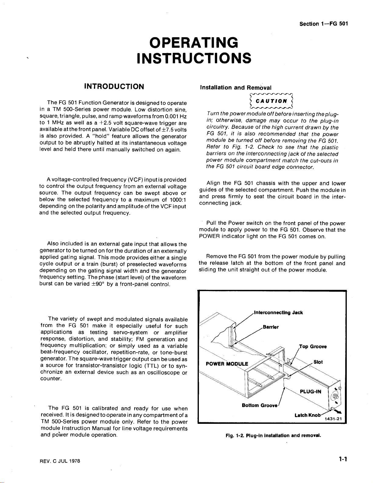
Installation
e,
guidesofthe
a
:1
e
ndpress firmlytoseatthe
connectingjack.
module
POWER
therelease
sliding
N
S
an
d R
emoval
Turnthepowermod
in;otherwise,damage
cίrcuitry
FG
mo
R
barriersonthe
p
t
heFG
Alignth
PullthePower
R
.Becauseofthe
501,itis
d
ule
efer
to
ower
module
501
to
indicator
emovethe FG501
theunit
alsorecommen
be turned
Fig.1-2.Checkto
interconnecting
compa
circuit
e FG501chassis
selected
switc
applypowertothe FG501
lightont
latchatthe
straight
off
board
Section1-FG
ule
off
before
insertingtheplug-
may
occurtotheplug-in
high current
d
edthatthep
before
removingtheFG
see
th
atthe
jackofth
r
tment
matchthecut-outs
edge
connector
wit
hthe
upperand
compartment.P
circuit
h
onthefrontpaneloft
he FG501
fromthe
bottom
outoft
he p
ushthemodule
board
.
comes
power
module
ofthe
ower
Observe
frontpanela
drawnbyt
owe
501
plastic
e
selecte
.
inthe
hepower
thatth
on
.
by p
module
.
501
he
r
.
d
in
lower
in
inter-
ulli
ng
nd
e
Thevariety
fromtheFG
ap
p
lications
response,
fre
q
beat-freque
generator.The
α
source
chron
counter
T
received
TM
moduleInstr
andpower
REV.C
distortio
uency
multiplication;orsimply
n
for
izeanexternal
.
h
eFG
.Itis
500-Series
module
JUL
197
of
sweptandmodulatedsignals
501mak
as
cy
oscillator,rep
sq
tra
n
501iscalibratedand
designedtooperateinany
power
uctio
8
eitespecially
testing
n,and
uare-wave
sistor-transistor
n
Manual
operation.
servo-system
stability
etition-rate,
trigger
logic
device such asanoscilloscope
module
for
only
line
available
useful
for
suc
or
amplifier
;
FM
generationan
u
sedasα
outp
utcan
(TTL)
ready
compartmentofα
.Refer tothepower
voltagerequir
variable
ortone-burst
be
usedas
or
to
syn-
for
usewh
ements
en
or
h
d
Fig.
1-2.Plu
g-ininstallatio
n andr
emoval
.
Page 7
r
atingInstru
O
p
e
reusing
Befo
OperatingCon
escriptionofthef
d
indicators
and
Output
outputoftheFG501isdesignedtooperate
T
he
voltage
load.Atth
improperly
aberrations
M
waveform
terminationis
(especially
en
following precautio
waveform
sourceinseries
atc
hing
E
xcessive
surethatwaveform purity
1
.Use q
.
M
2
a
3
.
Use q
ctions-FG
theFG501
siderationsinthis
i
n
F
n
ections
Con
ehigher
terminated
onthe outputwaveform
discussion)
amplitude
distortion orab
withsineand
uality50Ω
keall
uality
amplitude
.Loa
.
lesslik
elytooccur
ns
connections
attenuators,ifnecessa
to
501
O
PER
ΝΟΤΕ
fo
rth
ont-panel
r
ig.1-3
.
with50
frequencies,
:
coaxial
Ω
output
dsless
errations
triangle
sensitivecir
waveforms)
is
cables and
tightand as s
ATING
time,readthe
e
first
section
controls,
and
workinginto
an unter
willcau
than 50Ωwillred
thelower
at
preserved,
cuits
an
connectors,
mi n
excessive
se
(see
Impedance
to
due
frequencies
.However,
observethe
connectors
h
ort
as
ry,to
.
CO
dthe
as α
α 50
ated
ucet
improp
ossible
p
reduce
or
he
.
Ω
er
to
.
N
SID
difference
thetest
identical
p
ulse
thevoltage
preven
throug
con
eno
R
measuringt
ch
considered.If
least
FG501
cables,
generally
device,however,isless
combi
risetimeoft
risetime
equalsthe square
individual
under
theactual risetimesint
t
he device
ER
Wh
en
signal
determinatio
device
loss
Ifthereisαdo
amplitude
exceeds
t this
from
h α
do
stant
ug h
isetime
Iftheoutput
aracteristics
thecouplingcap
of
maintainp
to
and
herise
10 times
t
plus
the
errorin
can
ned
risetimes
he device
eac
of
risetimes.Conversely,t
test
canbefound
under
ATIO
com
uldtravelth
sho
and
time-d
voltageacross
will
occurring,theoutput
b
loc
Falltime
pulse
associatedequip
of
therisetimeoft
greaterthanthe
he monitoring
be ignored.Ifthe
h componentmaking up
test
N
S
p
arison
ns
compressed;orinsome
be
±10V,it
king cap
ulse
falltimeofαdevice,
or
troduced
of
willhave
rootofthesum
hesystem
.
measurements
are
made,th
roug
elaych
aracteristics
theoutput
mayshort
acitor to
acitorand
flat
ness
.
fromtheFG501
he d
combine
oscilloscope
willnot
rise
t
han 10 times as long as
the
testingsystem,
tobe
herisetimeofthedevice
fromthesame
areknown
or time
two
signals
e
coaxial
h
the
me
evice un
or
eterminedfromth
d
of
cables
.
load,th
e
cases,
output.To
the
mustbe
loadmust belon
ntmayhavetobe
d
exceed1ο/οand
falltimeofthetest
the
t
he sq
relations
coupled
load.
The
is
use
herisetime
t
der
testisat
risetimesoft
andassociate
the
system.This
uaresofthe
hipif
except
from
wit
output
time
d
for
he
t
actual
that
h
if
g
d
he
e
all
of
4
.Use
terminators
avoid
reflections
more
.
5.E
nsurethatattenuators,
ad
equate
waveform(app
P
its
am
T
transmitting
pedance,
loss.Signal
dielectric,
few
tionin
as s
power-
u
ower
he p h
feet
h
tputisdeterminedbythe
o
p
litude,andtheamount
ysicaland
velocity of
isproportionaltothe
ofcablecan
fEkst-risepulse.Itisimportanttokeept
α
ortaspossible
impedance-matching
or
n
usi
whe
h
roximately0.5Wintoα50
cable d
d
loss,
ng long cables,i.e
terminations,
andli
ng capabilities
offset
of
h
electrical
eterminethe ch
prop
uetoen
attenuatehigh-freque
.
aracteristicsoft
c
agation,
ergydissipatio
frequency
selecte
and
voltage
amount
devices
six
feet or
.,
etc
.have
forthe
Ω
aracteristic
output
load)
.
d
waveform,
selected
he pu
of
i
n thecable
n
therefore,
;
informa-
ncy
h
ese
signal
cables
to
.
lse-
im-
Impedance
R
eflections.Asαp
line,
eachtimeitencou
different t
generate
amplitude
amountofthe
b
ythe
tothe
mismatc
willbeof
lower,thereflection
reflectedsignal
or
subtracts
to
distortsthe p
M
atchingNetworks.
α
matching
for
impedances.Ifth
suc
h asthe1ΜΩ
an
oscilloscope,
M
atchi
ng
u
lse
travelsdownαtra
n
tersαmismatc
he transmission
han
t
a
nd
sent
d
andpolarityofthereflectio
ch
aracteristicimp
h impedance
the
backalon
encountere
ishigher
samepolarity
willbeofoppositepolarity
retur
ns before
from
ulsesh
apeand
impedance
eFG
input
the
transmissionline
gthe
edance
hantheline,th
t
the
as
the
theamp
The
501
impedanceofthe
litudeofthe
amplitude
followingdescribes
networksin
isdrivi
nsmission
h
,
im p
or
an
ne,αreflection
li
linetothesource.T
ns aredetermined
d
impedancein
ofthe cable
reflectio
e
applied
pulseisended,
.
ng αhig
must be
sig
relatively
to
h
vertical
REV.Β
nal;ifit
pulse.Th
methods
impedance,
terminate
edance
is
he
relatio
n
Ifthe
.
n
is
Ifth
e
.
itadds
is
low
inputfor
JUL
197
d
8
Page 8

FUNCTION
Selects
square,
output
and
ramp
duration
Operating
siderations
tional
information
AMPL
Concentric
SET
control.Varies
plitude
the
OUTPUT
from
less
(fully
ccw)
open
B130000-up)
below
trol
is
label
providesamaximum
15Vp-p
Selector
sine,
ramp,
and
waveforms.Pulse
waveform
is
1/2f.See
for
Control
with
of
waveform
connector
than
to
20 V
circuit(S N
.
8130000,
OUTPUT
open
circuit
triangle,
pulse
Con-
addi-
.
OFF-
am-
at
500
mV
p-p
For
SN
con-
and
of
.
OUTPUT
TRIG
Connector
Bsmconnector
vides
a+2.5Vsquare-
wave
trigger
6000load,
that
output
pre
into
POWER
when
the
Indicator
powerisap-
FG
501
.
Operating Instructions-FG
501
a
FREQUENCY
The frequency
triangle
waveforms
reading
Ramp
arid
forms
have
approximately1.6X
setting
with the
1
or
above
quencyofapproximately
2X
dial
three
lowest ranges
the
MULTIPLIER
tor
.
Provides
tion of
output
from
the
(calibrated)
approximately0.35%
full
scaleinthe
position
Hz
Dial
of
square
is
the
multiplier
pulse
a
frequency
multiplier
and
sine,
wave-
a
and
times
times
MULTIPLIER
settingonthe
selec-
vernier
selec-
frequency
fully cow
position
fully
.
dial
.
dial
at
fre-
of
to
of
ccw
OFFSET
Concentric
contrN
.
13130000-up,
pullout
able
from
provides
dc
zero
offset
(centered)
either--7.5V
or+7.5V
When
pushed
vides
zero
B130000
not
limits
.
off-set,
pull
below
does
offset
+5 V
PHASE
When
pulled
continuously
selection
output
level
(fully
cw)
or
starting
of the
waveform
(phase)
ccw)to-900(fully
referencedtothe
triangle
waveform00
point.Used
conjunction
GATE
INPUT
when
operatingingated
output
(burst)
Control
with
AMPL
For
S
control
a
var-
voltage
(fully
cew)
(fully
cw)
in
pro-
For S
control
out
and
are-5Vto
Control
out provides
variable
gated
start
from
+90
sine
with
the
connector
mode
.
MULTIPLIER
N
Selects
in9decade
provides
positions
to
.
N
lowest
positions)
generator
desired
voltage
Bnc
connector
ing
an
for
controlling
frequency
generator.A
provides a
rangeof1000:1
Selector
frequency range
steps
three
(between
three
that
and
"hold"
the
multiplier
hold
the
outputatany
instantaneous
level
.
for
external
apply-
voltage
the
output
ofthe
10Vinput
frequency
.
0
OUTPUT
in
Bnc
vides
form
FUNCTION
Connector
connector
the output
selected
that
wave-
by the
selector,
pro-
GATE
INPUT
A
brie
applyinga+2
gating
generator
connector
signal to
.
Connector
V
to
+15
for
the
V
1431-13A
REV
Fig.1-3.Operating
MAR
197
C,
9
controls
and
connectors
.
Page 9
O
perating
intoα50Ωattenuator
oscilloscope
capacityofthe
input
Α
p
rovides
match
ingcon
Instructions-FG
capacity
simple
minimum
impedance
ditionsmust
input
.
device.Distortion
.
resistive
attenuation
withthe
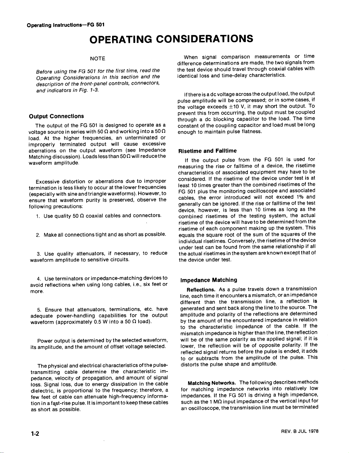
(R,
+
R
,+Ζτ+
and
R,
+
erefore
Th
:
R
ιRz=ΖιΖz;
orRι
R
and
501
andα50Ωtermination
The
attenuator
can
impedance-matching
illustrated
is
exist
Ζτ
)
R
Z,
Z,+
andRιΖι
=Ζτ
z
=Ζι-\Ι
illustrated
:
τ
R
m
R
z
2
must
R
z
(Ζτ-Ζι)
usteq
equal Ζτ
=
Ζ
2
network,
ualΖ,
R
z
Ζ
τ
_
Ζ
isolates
caused
be
inFig.1-4
(Ζτ-
,
at
the
by
n
etworkthat
the
follow-
ΖI)
the
input
this
.
To
.Imp
Fig
.
1-4
attenuation.
Α
signal
(
Ζ2)en
cou
greater
han1a
t
edance-matc
Ε2)app
(
n
tersαgreater
lied
lessthan2
nd
hingnetwor
t
hehigherimp
from
voltage
(Z2/Z,)
k th
atten
at pr
u
ation(
:
ovides
edance
Α2)wh
minimum
source
ichis
F
or
Ζ,eq
Th
example;to
uals
50
erefore
matc
ΩandΖ2eq
:
R,=-\/i25-(125-50)
an
dR2
=
ncon
Wh
e
surroun
provide α
mindthatthe
is
determined
inner
the
cond
uctor.το=
structing
dingthecompo
transitionbetwee
characteristic
bythe
conductortothe
138/
diameterofthe outer
diameteroft
tant
(1 in
heinnerconductor.ε
air)
.
AttenuationRatios.Thou
d
es minimum
provi
im pedance-matching
oneend
signal(Ε
en
counters
t
han1andless
does
ap
,)
not eq
p
lied
voltage
α
t
han2,as
Α,=
fromthelower
h α 50Ωsystemtoα
uals
125Ω.
50
1252550
suchα
nentssh
evice,theenvironment
d
ould
nthe im
impedance
ratiobetwee
ε
log,o
heoutsi
n
t
nsidediameteroft
i
D/d,whereDis
conductor,an
is
hthe
g
uatio
atte
d
evice,theattenuatio
n forα purely
n
ualthatseenfrom
impeda
attenuation(Αι
follows
Ez
:
=
+
Ζτ
Ω
125
=96
.80
.6
Ω
64
-
b
e
also
p
designedto
edan
ces
α
coaxialdevice
of
de diameter
t
d d
the
networ
he outside
is
dielectriccon
kin Fig.
nas
theotherend.Α
ncesource(Ζ
whichisgr
)
1
system,
.Keep
outer
he
inside
the
resistive
seen
from
eater
in
of
s-
1-4
,)
exampleofmatc
Inth
e
illustrated
The
different
(lessthan
attenuatio
R,)
Durationof
d
urationoframp
Th
e
ualtot
eq
waveform
greater,
he h
freque
he
retrace/off
t
α dutycycle
approximately
MULTIPL
from
pproaching
a
IERsettings
10
ms
2ΧFREQUEN
_Ετ__
Az
=
Ε
ιRz
Α
'925
.8+96
96
Α2=
64
.6
n
etworkcan
n
ratios
betweenΖ,an
amps
R
alf-cycle
andPulses
ncy.
timeofthe
For
timeissuc
of
approximately
1.6Χ
FRE
less
100
ο/ο
Hz
;
i.e.,
ms,which
d
ial
to
100
CY
_EL
R'
+
hing 50Ωto
+1=1
.8
+
50
b
addi
by
thejun
d
an
dpu
lse
sine,
TIPLIERsettings
MUL
hthatthe
ο/ο, i.e.,
80
UEN
CY
Q
than1,the
frequency
setting
.
R'
+
1
125Ω.
.77
1=4
.44
emod
ified
to
p
ctionof
herresistor
R,
an
ng anot
waveformsisalways
square,ortriangle
of
waveformhas
ncyequals
fre
que
dial setting
Hz
retrace/off
results
equals
i
n duty
approximately
time
rovide
d Rz.
1
or
.
For
cycles
is
REV
197
Β
JUL
.
8
Page 10
O
PER
ATIO
OperatingInstru
ctions-FG
501
N
Free-
Runn
following
T
he
waveform
1.SettheA
p
osition
andtheOFFSETcontroltot
position.Ch
2.Set
waveform
ingOu
tput
procedure
withvariable
output
MPL
controltothefullycou
eckthatthePHASE
FUN
CTIO
.
the
(seeFig.1-5)
providesαfr
frequencyand
n
co
N
selector
trolis
ee-running
amplitude
nterclockwise
(cen
he 0
pushed
toth
e d
tered)
in (off)
esired
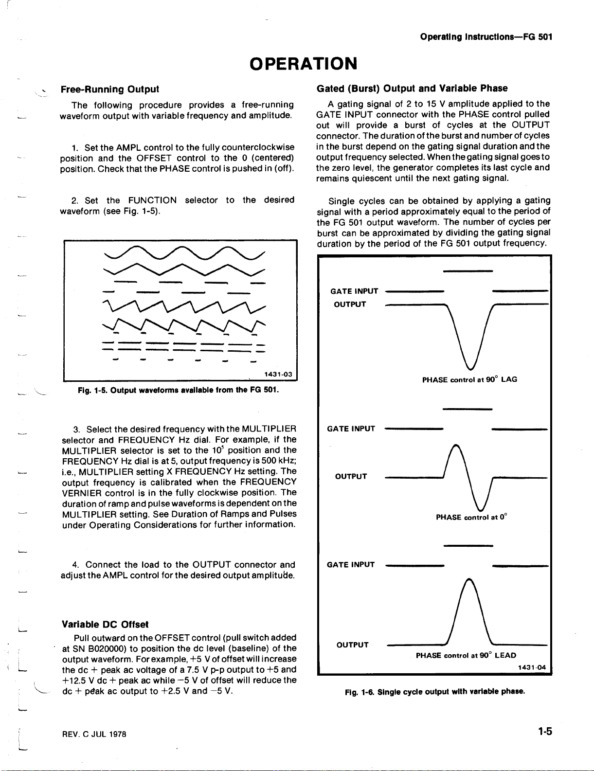
Gated(Burst)
GAT
.
out
connector.T
intheburst
output
.
the
remains q
signal
t
b
durationbyt
Output
Α
gating
signalof2to15Vamplitude appliedtothe
EINPUTconnector
will
provideαburst
an
wit
hedurationofthe
dependonthegatingsignaldur
frequencyselected.Whenthegati
zero
level,the
uiescent
Si
ngle
cycles
withα
heFG
501 ou
urst
can be approximated bydividing
E
INPU
GAT
generator
un
tilth
enext
canbe obtained
periodapproximately
tput
waveform.T
he p
eriodoftheFG
T
OUTPUT
dVariablePhase
hthePHASEcontrolpulled
of
cycles
burstandnu
completes
attheOUTPU
mberofcycles
atio
ng
signal
its
last
gating
signal
by applyingα
equaltotheperio
henumber of
thegating
501
outputfreque
n andt
goes
cycle an d
.
gati
d
cycles pe
signal
ncy
T
he
to
ng
of
r
.
Fig.
1-5
.Outputwaveforms
3.Selectthe
selectorand
MULTIPLIER
FREQUEN
i.e.,
output
VERNIER
d
urationof
MUL
underOp
CY
MULTIPLIER
frequency
control
rampand
TIPLIERsetting.See
eratingConsid
desiredfre
FREQUEN
selectoris
Hzdial
settingΧFREQUEN
calibrated
is
isinthe
pulse
availablefromt
quency
CY
Hzdial
settothe
at5,output
is
fully
wit
whenthe
clockwiseposition.
he FG501
htheMULTIPLIER
.
Forexample,ifthe
10
5positionandth
freque
ncyis500kHz
CY
Hz
FREQUEN
waveformsisdependentont
Duration
erations
ofRampsandPulses
for
further
setting.Th
information.
4.ConnecttheloadtotheOUTPUTconnectorand
adjusttheAMPLcon
Var
iable
DC
Pull
outwardontheOFF
atSN
13020000)topositio
t
waveform.Forexample,+5V
outpu
+peak ac voltageofα 7.5V
the
do
+12.5Vdo+peakacwh
d
o+pdakac
trol
forthedesired outputamplitude.
Offset
SETcon
nth
e do
trol
level
ρ-ρ
ile-5V
of offset
outputto+2.5Vand-5
switcha
(pull
(baseline)ofthe
of offset
willincr
outputto+5
willred
V
.
.
The
dded
ease
and
uceth
GATEINPU
Econtrolat90°L
PH
AS
T
AG
e
;
e
CY
OUTPUT
he
0
trol
at
°
1431-04
GAT
E
OUTPUT
I
NPU
PHASEcon
T
PHASEcontr
ol at90°LEAD
e
Fig.
1-6.Single
cycleoutput
withvariablephase
.
REV.C
JUL
197
8
Page 11
Op
erating
Instructions-FG
501
T
he ph
ase
(start level)ofthewaveform
varied
±90° bypulling
either
(centered)position
counterclockwise
(seeFig.1-6)
burstisreferencedtothe
p
oint.
Output
d
uration
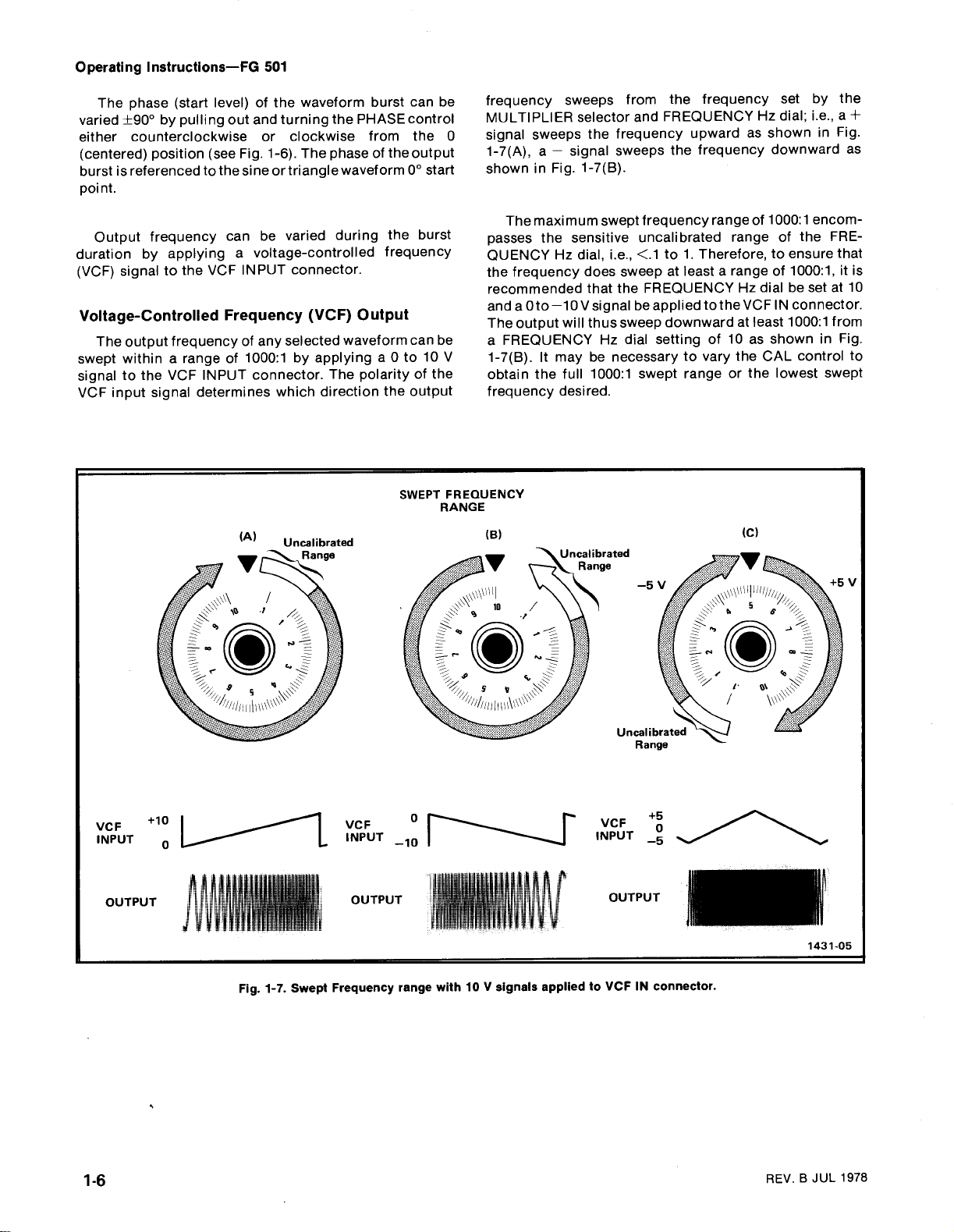
(VCF)
V
oltage-Controlled
T
swept
signaltot
V
CFinput
frequency
by
applying
signal to
he outputfre
withinα
heVC
signal
t
h
V
e
quen
rangeof1000:1by ap
FINPUTco
determineswhich d
out
and
turningthePH
or
sine
or
e
canb
variedduringt
α voltage-con
C
FINPUTconn
F
requency
cyofany
selected
n
nector.Thepolarity ofthe
k
wise fromthe
cloc
T
h
haseoft
.
e
p
triangle
waveform0°start
trolled
ector
(VCF)
waveform
plyi
irectio
burst
can
Econ
he ou
trol
tput
AS
heburst
uen
freq
cy
.
Output
can
be
ng α0to10V
ntheoutput
S
WEPTFRE
be
0
RANG
frequency
TIPLIERselector
MUL
signal
1-7(Α),α-
sh
owninFig.
Th
p
assesthesensitive
Q
UEN
hefrequen
t
sweeps
sweepsthefrequencyupwar
signal
maximum
e
H
z
CY
dial,i.e.,<.1to1.Th
cydoes
from
and
sweeps
1-7(Β)
.
swept
fre
uncalibratedrangeofthe
sweepatleastαrangeof1000
recommendedthattheFREQUEN
an d α
Oto-10VsignalbeappliedtotheVC
T
he output
α
FREQUEN
1-7(Β) .Itmay
obtai
frequency
UEN
CY
O
willthussweepdownwardatleast
CY
Hz
dial settingof10
be
necessarytovary
nthefull
1000:1swept
desired.
E
the
fre
FREQUEN
the
frequency
uency
q
d as sh
set by
Hz
d
ial
CY
; i.e.,α+
own
downwar
quencyrangeof1000:1en
erefore,toensureth
CY
Hz
dial
setat10
be
FINconnector
1000
CA
nin Fig.
L
control
range
asshow
the
thelowest
or
t
he
inFig
d as
com-
FRE-
:1,
it
:1
from
swept
.
at
is
.
to
V
C
INPU
OUTPUT
F
T 0
+10
VC
INPU
(
ΙΙΙΙΙΙΗΙΙΙΙΙΙΙΙΙΠΠΠΠΠΠλΓΙΠΜ
Fig.
~
1-7.SweptFrequen
ΙΙΠΓ
1
OUTPUT
F 0
T
_10
ange
cy
r
with10Vsignalsap
plied
V
C
F
I
NPU
T
OUTPUT
toVCFIN
+5
0
_5
conn
ector.
REV.Β
1431-05
JUL
1978
Page 12
An
input
signal
level
will
also
the
center
frequency
FREQUENCY
Since
theVCF
relationship,
minedfrom
H
oldMode
the
theVCF
Three detented H
the
lowest
switchingtoany
canbestopped
there
until
three
the
that
varies
symmetrically
sweepthe
HzdialasshowninFig.
input
frequency
one
at
its
MULTIPLIER
generator
setby
the
amplitudevsfrequencyisα
output
input
amplitude
OLD
positions
MULTIPLIER
the H
of
instantaneous
OLD
symmetrically
MULTIPLIER
range
.
are p
selector
positions,
voltage
selector
α0
about
about
selector
1-7(C)
can
rovided
positions.By
the generator
level
settingischanged
.
be
between
andheld
an
linear
d
eter-
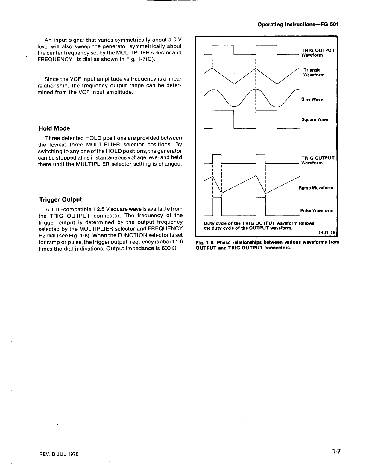
Operating Instructions-FG
V
d
.
TRIG
W
aveform
Triangle
aveform
W
SineWave
SquareWave
TRIG
W
aveform
501
OUTPUT
OUTPUT
T
rigger
the
trigger
selected
Hz
for
times the
Out
ATTL-compatible+2
TRIG
OUTPUT
output
the
by
(seeFig.1-8).When
dial
ramp
or pulse,
d
ial
put
.5Vsquare
connector.The
d
etermined
is
MULTIPLIER
the
thetrigger
indications.Output
output
isavailablefrom
wave
frequency
by the
selector
FUNCTION
output
and
FREQUENCY
selectorisset
frequencyisabout1.6
impedance
of
frequency
600Ω.
is
the
Duty
theduty
Fig.
1-8.Phase
OUTPUT
cycleofthe
cycleofthe
elationshipsbetween
r
and
TRIG
TRIG
OUTPUT
OUTPUT
OUTPUT
connectors
waveform
waveform
various
.
.
follows
waveforms
1431-18
from
REV.Β
JUL
1978
Page 13
Oper
ating
Instructions-FG
501
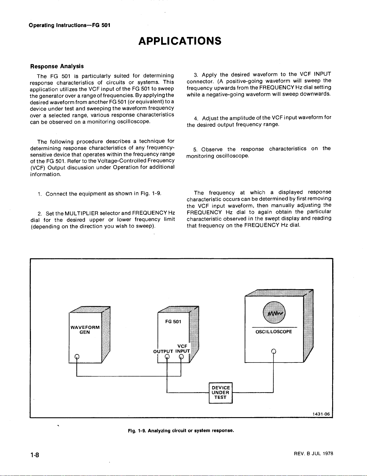
R
esponse
T
heFG501
responsecharacteristics
application
t
he
generator
desiredwaveform
device
over
can
be
The
determining
sensitive
oftheFG
F)
(V
C
informatio
1.Connecttheequipment
2.Setthe
dial
(depen ding
Analysis
is
particularly
utilizestheVC
rangeoffrequencies.Βγ
over α
anotherFG501
from
dertest
un
selectedran
α
observedonαmonitoring
followingproceduredescribes
devicethatoperates
501
OutputdiscussionunderOp
n
forthedesire
and
sweepingthewaveform
ge,
various
responsecharacteristics
.Refer toth
.
MULTIPLIER
d
upper
thedirectionyou
on
A
dfordetermi
suite
circuitsorsystems.Th
of
Fin
putoft
he FG501toswee
(or
equ
nse ch
respo
oscilloscope.
technique
α
of
any
withinthe
eVoltage-Controlled
as s
selectorand
or
frequency
eration
h
owninFig.
FREQUEN
lower
wishto
for
fre
que
sweep)
PPL
applying
ivale
frequency
aracteristics
frequency-
F
nt)to
reque
d
ditional
a
1-9
ncy
.
ICATIO
ning
is
p
the
α
for
range
ncy
.
CY
Hz
limit
N
S
3.Applythe
connector.(
frequency
whileαnegative-going
4
t
hedesired
5.Observetheresponse
monitoring
The
aracteristic
ch
the
FREQUEN
characteristic
that
upwardsfrom
Adjustthe
.
frequency
V
CFinput
CY
frequency
esired
d
ositive-going
Α
p
amplitude
output
oscilloscope
fre
occurs
waveform,
Hz
dial
observe
theFREQUEN
on
q
atwhich
can
d
waveform
waveform
theFREQUEN
waveform
uency
.
be
to
inthe
will
oftheVCFinput
range
ch
α
eterminedby
d
t
henmanuallyadj
againob
swept
CYHzdial
toth
e
VC
will
swee
CY
Hz
dial
swee
p
d
ow
waveform
.
aracteristics
layedrespo
dis
p
first
usting
tainth
eparticular
display
and
.
FINPU
t
p
setting
n
wards
t
on
nse
removing
the
reading
T
he
.
for
he
Fig.
1-9.Analyzingcircuitor
system
response.
REV.Β
JUL
1978
Page 14
Operating
Instructions-FG
501
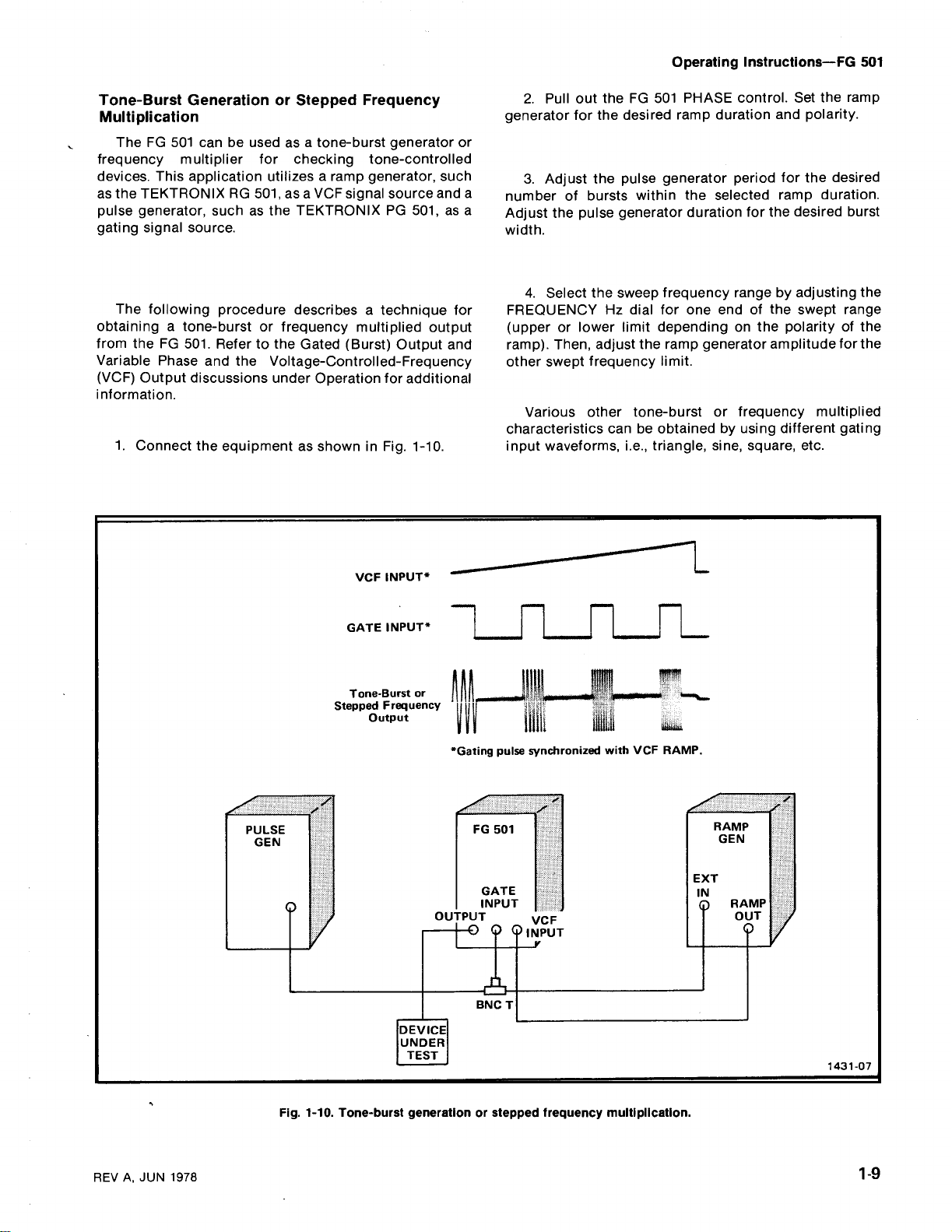
Tone-Burst
M
ultiplication
The F
fre
q
uency
devices
Generationor
G
501
canbeusedasαtone-burst
lier
multi
p
T
hisapplicationutilizesαrampgen
.
astheTEKTRONIXRG
p
ulse
generator,
gating
signal
The
following
obtaini
ng α
from
theFG
V
ariable
(VCF)
Ph aseandtheVoltage-Controlled-Frequency
Output
information
1.Connectthe
suchasth
source
proce
tone-burstorfrequency
501
.Refer totheGated(Burst)
discussions underOp
.
equipment
Steppe
for
chec
501,asαVCF
e TEKTRON
.
d ure describes
asshowninFig.
d
F
requency
generator
kington
e-controlle
erator,
signal
sourceand
IXPG
α
techniquefor
multiplied
501,
suc
as α
output
Outputand
erationforadditional
1-10
.
or
generator
d
h
α
n
umber
Adjustthe
width.
FREQUEN
(upper
ramp).Then,adj
other
h
c
input
2.Pull
outtheFG501
PHASEcontrol.Settheram
forthedesiredrampduratio
3.Adjustthepulse
of
bursts withintheselecte
pulse
4.Selectthesweepfre
CY
Hz
or
lower
swept
frequency
V
ariousotherton
aracteristics
can
generator
d
generator
uration
quen cyran
dial
for
one
limit
de
pen
dingont
ustthe
rampgeneratoramplitudeforthe
limit
.
e-burst
be obtainedbyusi
periodfor
en doftheswept
frequency
or
waveforms,i.e.,triangle,sine,square,
he d
.
esire
uration
n an d
d
ram
polarity
t
p d
forthedesiredburst
gebyadj
ustingt
he
range
he p
olarityoft
he
multiplied
ngdifferent
etc
gating
.
p
d
.
V
FINPUT*
C
GAT
E
Tone-Burst
Stepped F
O
NPUT*
I
re
utput
r
o
en
cy
qu
1141' ίάϋυυ
*Gating
pulse
synchronize
ν
ι
withVCF RAMP
d
.
REVΑ,
JUN
197
1431-07
Fig.
1-10.Tone-burstgeneratio
n orste
ppedfr
equencymultiplication.
8
Page 15
S
PE
CI
F
ICATIO
N
Section2-FG
501
erformance
P
electricalch
Th
e
F
G
501 has been
b
etween
temperature
noted
temperatureab
F
F
.
requency
R
ange
Sine
andTriangle
Accuracy
R
esolution
+200Cand
b
orcedair
C
haracte
W
ave,Squ
D
andis
+50°C
PERF
operatingatan
A
N
Conditions
aracteristics
calibratedatanambient
+300C
etween0°Cand
circulationisrequ
ove
+40°C
.
r
istic
areWave,
O
PE
S
are
vali
d onlyifthe
temperature
ambient
unlessotherwise
iredforamb
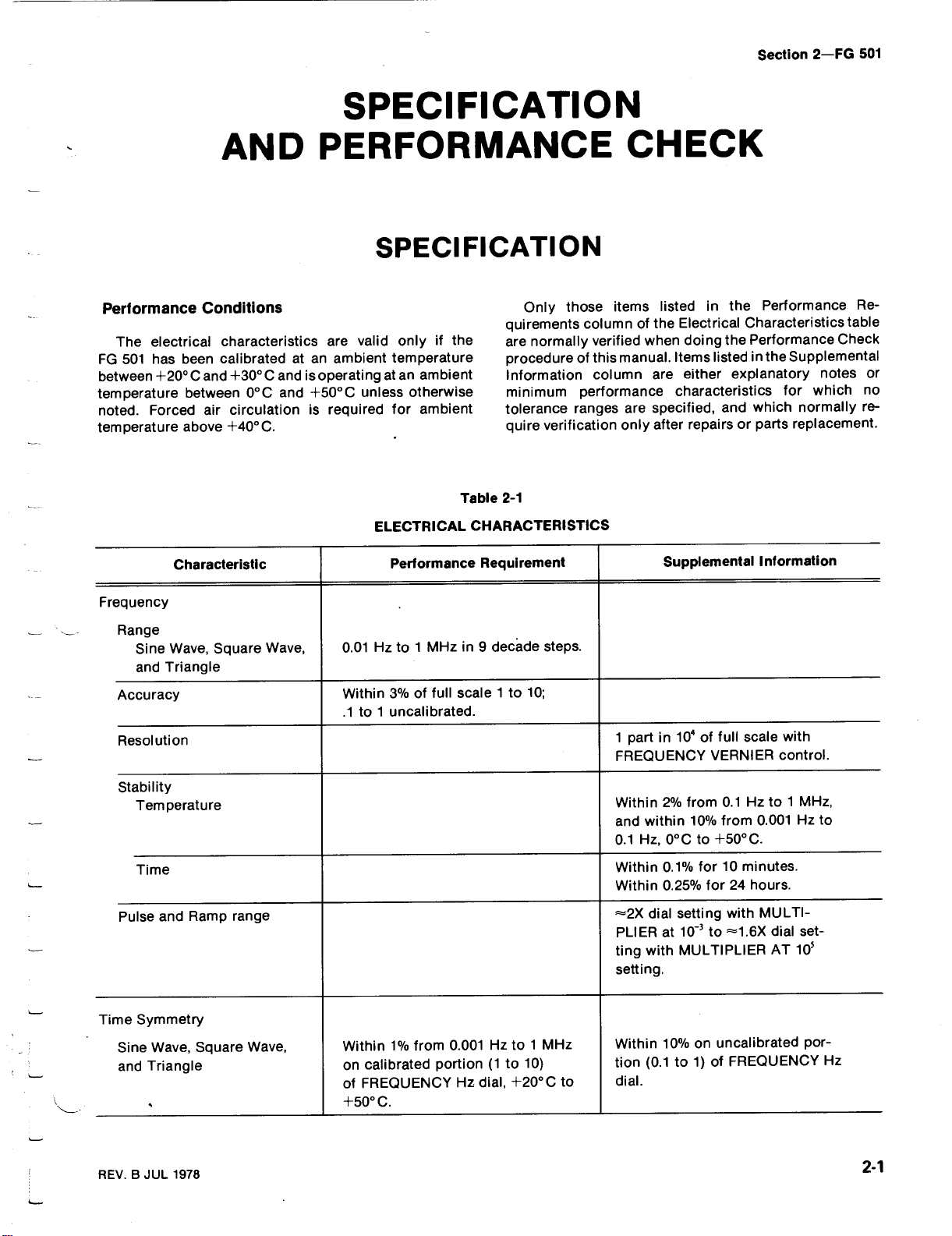
ELECTR
P
erformance
0
.01Hzto1MHz
W
ithin3ο/οoffull
.1to1uncalibrated
RM
A
N
CIFICATIO
Onlyth
quirements
are
normally
procedureofthis
Informationcolum
mi nimum
ient
ICA
LCHARACT
scale1to10;
Table
R
equirement
in
9decade
.
toleranceran
q
uire
verification
2-1
ER
steps
C
E
C
HE
C
N
ose
items
listedin
columnofth
verifiedwhendoing
manual.Items
n are
erformancecharacteristics
p
ges
are sp
only
ISTICS
.
1
partin10°offull
FREQUEN
lectrical
e
E
listedintheSupplemental
eitherexp
ecified,
afterrepairs
Suppleme
CY
VERNIERcontr
K
t
he P
erformanceRe-
Characteristics table
P
the
and
orp
n
talInfor
scale
erforma
lanatory
whic
nceCheck
notes or
whic
for
h normallyre-
artsrep
matio
wit
lacement
h
ol
h
no
.
n
.
Stability
Temperature
Time
P
ulseand R
Time
Symmetry
SineWave,Squar
andTriangle
REV.Β
JUL
197
ampran
8
ge
eWave,
W
ithin1ο/ο
on
calibratedportion(1
of
FREQUEN
+50°C.
from0.001Hzto1MHz
CY
Hz
dial,
to
+20°C
10)
to
W
ithi
n 2
ο/ο
from0.1Hzto1MHz,
andwithin10
0
.1Hz,0°C
ithi
n 0.1ο/ο
W
W
ithi
n 0
-2Χdial
PLIERat10-'to=1.6Χ
ting
withMULTIPLIER
setting
W
ithi
n 10
tion (0
d
ial
.
.1
.25%
.
to
ο/οfr
+50°C.
to
for
10 minutes
for
setting
ο/οon
withMUL
uncalibratedpo
1) of
om
24hours
FREQUEN
0
.001Hz
dial
AT
.
.
TI-
set-
10
CYHz
to
5
r-
Page 16

Specificatio
Amplitu
d e
Stability
Tem
Time
H
oldM
Offset
n andPerformance
C
h
aracteristic
(excluding
erature
p
ode
offset)
Stability
k-FG501
Chec
P
erformanceRequirement
S
N
B130000-up
circuit.10
Sine,
triangle,andsquarewave
amplitudes
singlesettingofA
.
trol
B
elow
n
trolprovi
co
circuitand7.5Vρ-ρin
50Ωload.
Table
2-1
(cont)
:
20
V ρ-ρopen
V
into50Ω
ρ-ρ
matched
NΒ130000,OUTPU
S
withi
MPL
ITUDEcon-
des 15Vρ-ρopen
to
load.
n 5ο/ο
for
SupplementalInfor
P
ower-s
upplylimiting
p
ressionofoutputwaveform
w
hen
imum
n
eously
maximum
offset
.
amplitudeand
are
used
mation
causes
simulta-
com-
max-
T
1MHz
Within2ο/ο
Wtihin10
from0.1Hzto
ο/ο
from
0
0.1Hz,0°Cto+500C
ο/οfor
With
in0
Within 0
Within
h
ourat
.1
.25%
ο
/οoffull
5
+25°C
10 minutes
for
24hours
out
on
0
.001Hzto
.
putvoltagein
.001Hzrange
.
.
.
1
.
Amplitude
I
O
n
to
p
en
Into50ohmLoa
R
ange
IntoOpenCirc
Into50ohmLoad
Output
Trigger
Impedance
Outpu
Amplitu
F
reque
t
de
ncy
TriangleandRam
L
inearity(b
10%
and 90ο/
etween
οpoints)
Circuit
u
p
it
-7.5
k
pea
offset
least
V
5V
V
signal
.
+
α
V
Ω
.
50
SNB130000-up
S
N
below
d
SN
B130000-up
N
below-Β
S
At
least+and-15V
plus
offset
SNB130000-up:At
:+or
Β
130000:+or-
+or-5
:
130000:+or-2.5
.
least+and
-6Vpeaksignalplus
SNb
elowΒ130000:At
and-5V
offset
+2.5V
peaksignalplus
.
square
waveinto
600Ωload.
Same
as
freque
ncyatoutputcon-
nector
.
1
With
100
after
Within2
excludingfirst
switch
ο/οfrom0.001Hzto
in
kHzexcludingfirst200ns
switch
ο/ο
points
from
.
100kHz
to1MHz,
200nsafter
points
.
2-2
REV
C,MAR
197
9
Page 17
Table
2-1
(con
SpecificationandPerformance
t)
heck-FG501
C
R
am
p Duration
neWave
Si
Square
Outputs
R
isetime
Aberrations
P
ulse
E
xternal
Input
B
urstLength
C
h
aracteristics
Distortio
W
ave
andPulse
Duration
GateInp
Signal
ut
.
erating
+15V.
selected
gating
Information
dportion of
alid
from
Consider-
+2
V,but
Output
h gateinput.
output
pulsewidth
bursts
.
P
erformance
n
1
ο/ο
or less
0.5ο
/
1ο/ο
or less
2
.5%οor less
at105
100nsor
5%οor
put
nal
50
from0.001Hzto
οorlessfrom
from
MUL
less
less
measured
p
litudeat10Vintoexter-
am
Ω
load
1Hzto20
kHzto
20
100kHzto1MHz
from
TIPLIERsetting
.
.
Req
ρ-ρ
ement
ui
r
1
kHz.
100kHz
.
without-
z
.
H
.
Supplemental
=
1
(seeOp
2f
ations)
Appliestocalibrate
dial
only
+10°C
10%to90%
(seeOp
=
1
2f
ations)
S
quare
n
ottoexceed
are sync
Determinedby
frequencyand
eratingConsider-
.
(1to10).V
to
+50°C
.
.
waveatleast
h
ronizedwit
Ph
asing
Input
Impedance
E
xternalVoltage-
Controlle
(VCF)
Input
Output
Range
Slew
d Freq
F
R
ate
requency
uency
least
At
input
.Negative-goi
decreases
goingin
=10Χ
f_
Χ
MUL
fm
in
1000:1wit
freque
creases
MUL
TIPLIERsetting
h 10
n
g
ncy
frequency
TIPLIERsetting,
100
V VCF
voltage
ositive-
;
p
ntinuously
Co
to
+90°
triangle
.
-=1kΩ
.
-0.5V/μs.
variable
referredto0°sine
startpoints
from
.
-90@
or
REV
C,MAR1979
2-3
Page 18
SpecificationandPerformance
Check-FG
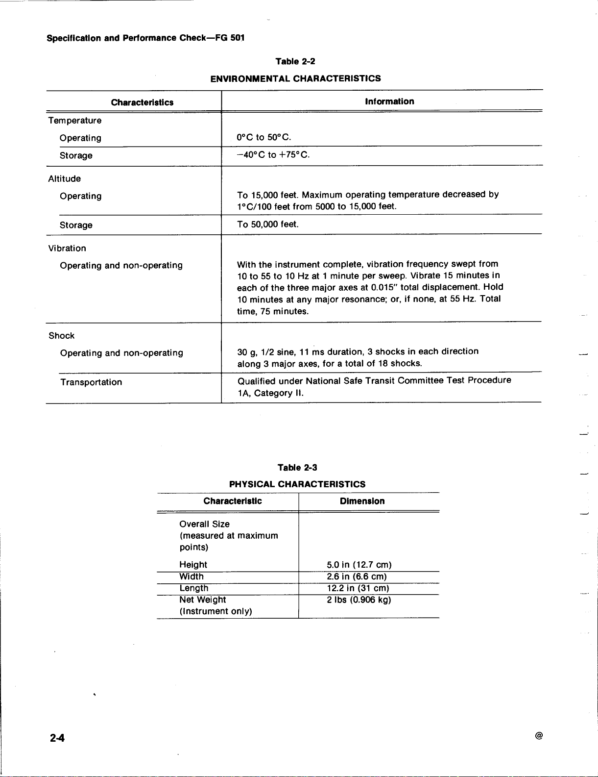
ENVIRONMENTALCHAR
501
Table
2-2
ACT
ER
ISTICS
Temperature
Operating
Storage
Altitu
de
Operating
Storage
V
ibration
Operatingand
Shoc
k
Operating and
Transportatio
C
ha
r
acteristics
non-operating
non-operating
n
0°Cto
-40°Cto
To
1°C/100
To
W
10 to55to
eachof
10
time,
30g,1/2
50°C.
+75°C.
feet.M
15,000
feet
50,000
feet
h
h
t
instrument
e
it
10Hzat1
thethree
minutesatany
75 minutes
sine,11ms
along3major
Qualifie
1Α,
d un
CategoryΙΙ.
aximum
from
5000
.
complete,
minute per
majoraxesat0
major
.
d
u
forαtotalof18
axes,
derNational
Informatio
operating
to 15,000
vibrationfreq
resonance;
ratio
n
,
3 s
Safe
Transit
n
temperaturedec
feet
.
uen
V
sweep.
.015"
hocksin eac
ibrate
totaldisplacement
r
,
ifnone,at55 Hz.
o
shocks.
Committee
r
ease
swept from
cy
15 minutes
h
directio
n
TestProcedure
d b
in
.Hol
Total
y
d
b
le
2-3
Ta
PH
YSICALCHARACTER
Characteristic
Overall
(measuredat
p
H
Width 2
Len
N
(instrument
Size
oints)
eight
gt
h
etWeight
maximum
only)
ISTICS
Dimension
5.0in(12.7cm)
.6
in(6.6cm)
12.2in(31
2
Ibs
cm)
(0.906 k g)
Page 19
Introduction
Th
isprocedurecheckstheelectrical
theFG501thatappear
manual.This
inspection
ma
nce.Ifthein
give
ninthisperformance
procedure
Theelectricalcharacteristics
ifthe FG501iscalibratedatan
+20°Cto+300C
of
0°C
ambient
procedure
facility to
strument
should b
and
+50°C.F
to
temperature ab
theSpecification
in
can
alsobe
determine
failstomeetthere
eperformed.
operatedatan
orced
air
ove
+40°C
PERF
use
acceptability
k,theadj
chec
inTable
ambient
ambient
circulationisre
.
O
characteristics
sectionofth
d by anin
2-1
are
temperature
temperature
RM
comi
p
erfor-
of
uirements
q
ustment
valid
only
uiredfor
q
ANC
of
is
ng
of
Table
SpecificationandP
E
CHE
Tolerancesthatare
ch eckp
n
2-4
rocedureapplytotheinstrume
otin
clude
testequipment
Test
EquipmentRe
T
he
testeq
uipment
requiredto
mentch
verifyth
Substitute
requirements.All
operatingwithin
performtheperforma
aracteristics
eperformance
equipment
C
tolera
erformanceCh
K
specifiedinthis
error
uire
d
q
listedinTab
listed
arethemin
oftheequipment
must meet
testeq
nce
uipment
.
ntunder
.
le 2-4,
nce check.
imumreq
r
exceedthe
o
is
ec
erformance
p
testand
or e
q
Test
u
assumed
k-FG501
do
uivalent,
equip-
uiredto
ndertest
state
tobe
is
.
d
P
erformance
Description
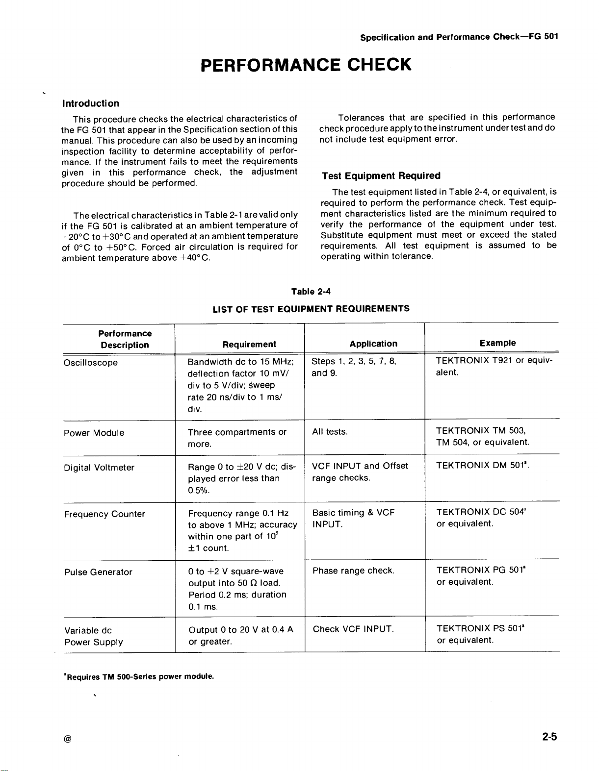
Oscilloscope
owerModule
P
DigitalVoltmeter
requency
F
P
ulse
Counter
Generator
L
ISTOF TESTEQ
R
equirement
Ba
ndwidt h doto15
deflectionfactor10mV/
divto5V/div;sweep
rate
20ns/divto1
d
iv
.
T
hree
compartments
.
more
R
nge 0to±20
a
p
layed
error
lessthan
0.5ο/ο
.
F
requency
to
above
withi
±1
count
0to+2Vsq
output
P
eriod0.2ms
0.1ms
range
1MHz;accuracyINPUT.
n on
epartof10
.
uare-wave
into
50
.
MHz
ms/
or
V dc;dis-VC
0
.1
Hz
5
Ω
load.
duration
;
UIPMENTREQUIREMEN
Applicatio
;
1, 2, 3, 5, 7, 8,
Steps
and9.
All
tests
FINPUTand
c
range
B
asic
timing&VC
Ph
aserangec
.
hecks.
heck
TS
n
Offset
F
.
E
xample
TEKTRO
alent
TEKTRONIXTM
TM
TEKTRON
T
EKTRONIXDC
or
equ
TEKTRONIXPG501
equivalent
or
IXΤ921 orequiv-
N
.
503,
504,orequivalent
IXDM
5018.
504
ivalent
.
.
.
8
8
V
ariable
P
ower
'RequiresTM500-Series
do
Supply
power
Output0to20Vat0.4Α
orgreater
module
.
.
C
heck
VCFINPUT.
TEKTRONIXPS501
orequivalent
.
8
Page 20
nan
P
Sp
ecificatio
P
e
rformance
Descriptio
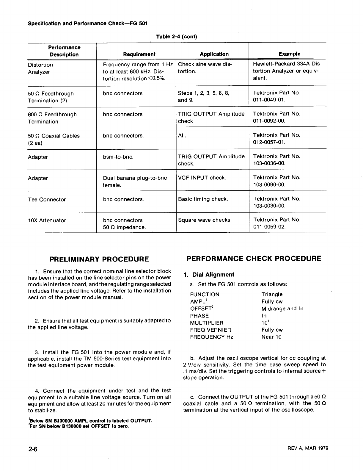
Distortion
Analyzer toatleast
erformanceCheck-FG501
d
n
Freq
tortion
Requir
uency
resolution
range
600
Table
ement
from1HzCh
kHz.
Dis-
<0
.5%
.
2-4 (cont)
eck
tortion.
Applicatio
sine
wavedis-
n
H
ewlett-
tortion
alent
E
xample
Pack
ard334ΑDis-
Analyzeroreq
.
uiv-
Ω
F
50
eedt
Termination
600ΩFeed
Termination
Ω
Coaxial
50
(2
ea)
Adapter
ter
Ada
p
TeeConn
Χ
10
ector
Attenuator
PRELIMINARYPR
hr
oug
h bnc
(2)
h bncconnectors
throug
Cables
connectors
bnc connectors
b
sm-to-bnc
Dual
female
bncconnectors
b
nc
50Ωimpeda
OC
.
banana
.
connectors
nce
D
URE
E
plug-to-bnc
.
.
.
.
.
Steps1,2,
and 9
.
TRIGOUTPU
check
All
.
TRIGOUTPUTAmplitude
c
heck
.
V
C
FINPUTcheck
timing
B
asic
S
quare
wave
PERFORMAN
3, 5,
TAmp
check
checks
6, 8,
litude
.
.
.
C
TektronixPartNo.
011-0049-01
TektronixPartNo.
011-0092-00
TektronixPartNo.
012-0057-01
Tektronix
103-0036-00
TektronixPartNo.
103-0090-00
TektronixPartNo.
103-0030-00
Tektronix PartNo.
011-0059-02
ECHECK
P
PR
.
.
.
artNo.
.
.
.
.
OCED
URE
1
.Ensurethatthecorrectnominal
hasbeen
modulein
incl
sectionofthe
2
t
he appliedline
3.Installth
applicable,in
thetesteq
eq
uipmenttoα
equipment
to
stabilize
'BelowSN Β
'ForSNbelowΒ130000
installedonthe
terface
udestheapp
.E
nsurethatall
4.Connectthe eq
board,
liedlinevoltage
power
voltage
e FG501
stalltheTM
uipmentpowermodule
suitable
and
allow
.
330000AMPL
line
andthereg
module
testequipmentissuitably
.
intothe p
500-Series
uipmentund
li
nevoltage
at
least
contr
setOFFSETto zero
selector
u
lating
.Refer to
n
ual
ma
20 minutes
ol is labeledO
.
ower
testequ
.
er
source.Turnon
line
selector
p
i
n
s
on
rangeselecte
t
heinstallatio
mo
testandthe
forthe equipment
TPUT
U
.
bloc
t
hepower
dapted
a
d
uleand,
ipmentin
.
test
d
n
to
if
to
all
k
1.Dial
2V/div
.1
slope operation.
coaxialcableandα50Ωtermination,
terminationattheverticalinputof
Alignment
α.SettheFG
FUN
CTIO
N
A
MPL'
E
T'
OFFS
PHASE
TIPLI
MUL
FREQVERNIER
FREQUEN
b.Adj
ms/
c.ConnecttheOUTPUToft
ER
CY
ustthe
sen
sitivity.Setthetime
iv
.
Set
t
d
controlsasfollows
501
Hz
oscilloscope
hetriggeringcon
:
Triangle
F
ully
cw
M
idrange and
In
10'
F
ully
εω
Nea
r
10
vertical
fordocoupli
base
swee
trolstointernal
he FG501th
wit
the
oscilloscope
In
ng
speedto
p
source
roug
hα50
hthe50Ω
.
at
+
Ω
2-
M
6
REVΑ,
A
R
1979
Page 21
d
.
Adjusttheoscilloscope
stabledisplayofapproximately1cycleper
e.CHECK-thatt
within±.5
Q
UEN
(For
waveform
f.Disconnectthe50Ω
oscilloscopeverticalinput
2.Sq
α.SettheFG
FUN
A
MPL'
OFFSE
PHASE
MULTIPLIER
FREQVERNIER
FRE
b.Setthe
at
1V/div
Trigger on+slope
mi nordivisionofthe
CY
Hz
easeίη
viewingthechangein
sothetrailing
uareWave
CTIO
T'
Q
UEN
sensitivity
N
CY
oscilloscopeforαdc-coupledverticalin
hedisplay
dialisadjustedbackandfort
Aberrations
501
controlsasfollows
Hz
andαsweepspeedof.05μs/div
.
trigger
stopsch
edge
canbeobserve
cable
and
.
Sq
F
ully
In
In
10
F
ully
8
.0
levelcon
anging
10
mar
frequency,
terminationfromth
and
Symmetry
uareWave
εω
5
εω
trol
division.
frequen
k astheFRE-
h around 10
positionth
d
.)
:
for
put
cy
Sp
ecificationan
α
.
e
e
.
g.Adj
ustthetest
the
entire
fallingportionofthe square
the
falltimeisa
n
ecessary)tobalance
h
.
Settheoscilloscopetime/divto.5μs/div.C
t
hataberrationsonthepositiveand
ofthesq
to
P
ositionthesq
exactdisplay
doesnot
1ο/ο
uare
i .
Setthe
j
.
Adjusttheoscilloscopesweepspeedand
displayone
k
.
Set
Ι .Ch
angethe
m.CHECK-thatthecen
).
η.Disco
pproximately 70
wave
oscilloscopeverticalsen
full
cycleoft
t
h
e
oscilloscopeΧ10
uare-wave
center
trigger
h
ift
h
r
s
izontallymoret
o
nnectth
dPerformanceCheck-FG501
oscilloscopetrigger
n
risetime
are
lessthan 5
.
e
50Ωcableand 50Ωtermination.
a
nd
he square
center voltage
polarity
from+slopeto-slope
ter
transitionoft
ο/ο
level
todisplay
wave.C
s
.Readjust
falltime
negative
.
sitivityto1V/div
waveίη 10
p
swee
han1division(withi
heckth
C281
.
front
corn
variables
divisions
magnifier
transitionto
he disp
(if
heck
ers
on
lay
at
.
.
.
.
n
ε.ConnecttheFG
coaxial
verticalinput.
d
five-divisio
graticule
(C281)
'Below$ΝΒ130000AMPL
'F
cableandα50Ωterminationtothe
ustth
d.Ad
j
e
test
n
isplay
e.Adjustt
f.Adj
rSNb
o
tire
the e
n disp
centerli
ustthe FG501highfrequency compensation
forαrisetimeofapproximately
elow
risi
he FG501OFFSETandAMPL
lay
ne).
Β
130000
501OUTPUTth
oscilloscopetrigger
ng p
ortionoft
(2.5divisions
controlIs
setOFFSETtoze
he square
above
70 ns(10
labeledOUTPUT.
r
o
.
roughα50Ω
oscilloscope
level
control
wave
.
controls
and
fora
belowthe
ο/οtο90ο/ο)
to
3
.Basic
α.SettheFG
FUN
A
OFFSE
PHASE
MULTIPLIER
FREQVERNIER
FREQUEN
b.Co
.
fromtheFG501OUTPUTtothefre
MPL'
CTIO
nn
Timing
N
T'
CY
Hz
ect
α 50Ωcoaxial
501
con
trols
as
T
r
F
ully
Off(in
In
10
F
ully
10
cable and50O
follows
iangle
5
:
εω
)
cw
(exactly)
termination
quencycounterinput.
REVΑ,MAR
1979
2-
7
Page 22
SpecificationandPerfo
HE CK-t
ε
.
C
followingc h
Counter
M
easurement
Interval
C
.1
SE
1SEC
1SEC
1SEC
art
.
F
re
heFG
F
G
ue
q
Dial
10
10
10
10
10SEC
1SEC
1SE
C
1SEC
rmanceC
501
501
ncy
Hz
1
1
1
1
heck-FG501
ngaccording
timi
F
G
501
M
ulti-
lier
p
10
5 1
MHz
(1
.03
10'
100
(103
10kHz
10'
(10.3kH
10'1kHz±30
(1
.03
100Hz±30Hz
10
2
(130Hz-70Hz)
1kHz
10'
(1.3kH
10'
10
(13kHz-7kHz)
100kHz
10
5
(130kHz-7
toth
F
requency
(t3°/οof
full
scale)
±30kHz
ΜΗτ-.970
kHz±3kHz
kH
z-97
±300
z-9
.7
Hz
kHz-.97kHz)
±300
Hz
z-700
kHzf3 kH
±30
.0
kH
Hz
kH
z
kH
kH
Hz)
e
ΜΗτ
z)
z)
z
z)
4
.VCF
α.SettheFG
FUN
AM
PL'
OFFSE
PHASE
MUL
Q
FRE
FEQUEN
)
b.Connect
termination
counter
ε.Adjustthe0-20
d.Co
he 0-20Vpowersupp
from
t
T
I
NPU
ter
adap
e.Adjust
thefreque
to0.001MHz
NPU
T
I
501
controlsasfollows
CTIO
N
T'
PLIER
TI
VERNIER
CY
Hz
50Ωcoaxialcab
α
fromtheFG
nput
forαreading
i
V
powersup
n
nect
α banan
a-to-
.Makesurethe gro
+
owersup
theFG
terminalont
501 as
goestothe
t
he p
ncy
of
.
Triangle
F
ully
cw
In
In
10
5
F
ully
εω
10
(exactly)
and50Ωfeedt
le
501OU
TPUTtothe
1MHz
of
.
ply
bnc ad
apterand
ly
output tothe F
for
undsideoftheba
he
p
plyoutp
utvoltagetoc
read
on
thedigital
:
zero
ower
h
roug h
frequency
volts
Ω
50
501VC
G
nan
a-to-
supply
co
out
cable
bnc
.
n
ha
u
nter
.
F
ge
d
.
Setthe
forFG
p
eriod
t
he
followingchart
Frequency
u
nter
Co
10SEC
1SEC
1SE
C
Disconnectthe
e
.
n
nectors
co
frequency
501
MUL
F
G
501
Dial
10
10
10
from
allunits
.
Hz
coaxial
counter
PLIER
TI
.
F
G
M
ultiplie
10
1
10-'
ca
coupled)tomeasure
(
dc
settings
slowerthan10
501
r
(t3°/οof
10.0ms±.33
(10
.33-9
100
ms ±3
(103
.3-96
1000
(1033
b
les,
terminationsa
2
Per
iod
full
scale)
ms
.67
ms)
ms
.3
m
s)
.7
±33.3ms
ms
.3-976.7ms)
nd tee
NPUTandconnect
I
digital
i
n
voltmeteris<-10
5.OUT
Disconnectthebnc
f
.
the
put
voltmete
HECK-thatt
g.C
h
.
Adjustthe
.Disconnectthecables
i
T
PU
α.Setthe F
FUN
CTIO
N
A
MPL'
E
T'
OFFS
AS
E
PH
TIPLI
MUL
ER
rin
V
ower
p
Signal
501con
G
.
he
.
Am
FREQVERNIER
FREQUEN
CY
Hz
cable
fromthe F
variable
voltage
supplyou
and
terminationf
litude
p
dopower
measured on
t
p
andWaves
trolsasfollows
Sinewave
F
ully
In
In
10'
F
ully
10
G
supplytothe
ut
voltagetozero
rom
:
cw
εω
501VC
t
hedigital
.
all
units
hape
F
.
SN
'Below
o
rSNbelowΒ130000
'F
0130000AMPL
control
setOFF
Is labeledOUTPUT
ET
to zero
S
.
.
AR
REVΑ,
1979
M
Page 23
Sp
b
.
Settheoscilloscope
2V/divsensitivity.Setth
slo
pe.Setthetime
base
vertical
etriggering
sweepspeedto
controls
fordc-coupling
tointernal,+
20μs
.
at
ecificatio
h
.
Disconnect
fromthedigital
n andPerformanceCheck-FG501
the
50Ωca
voltmeter
bleand50Ω
.
terminatio
n
nnect
c.Co
fromth
inputand
p
output
forSN
FUN
frontpaneloft
fromthe
6.OFFSE
e FG501OUTPUTtotheoscilloscopevertical
d
.
Turn
osition
.
e.CHECK-thatth
signalis310
belowΒ130000
f
.CHECK-th
CTIONselectorcorrespo
g.Disconnectthe50Ω
α.Setth
FUN
CTIO
A
MPL
OFFS
PHASE
MULTIPLIER
FREQVERNIER
FREQUEN
α 50
obtai
n α
t
he FG501
at
he FG501
oscilloscope.
TRan
ge
e FG501asfollows
N
T
E
CYHz
Ω
coaxial
triggereddisplay
FUN
epeak-to-peakamplitude
volts
for
.
he
waveform
t
.
terminationand 50Ωcable
and50O
cable
.
CTIONselectortoeac
SN Β
130000-υρ;
for
eachpositionofthe
ndstothatsh
:
Triangle
Fu
lly
ccw
OUT(SNB130000-up)
In
10'
F
ully
εω
10
termination
eac
of
.5
volts
37
own
onthe
7.TRIGOUTPUT
α.Setthe FG501
FUN
A
h
h
MPL'
O
FFSET'
PHAS
MULTIPLIER
FREQVERNIER
FREQUEN
b
.Setthe
c.Connectαbsm-to-bncadapterto
U
TPUT.Connectα50Ωcoaxial
O
toα600
terminationtothe
cilloscope
triggering
d.CHEC
greaterth
e
.Disco
tionfrombothunits
p
litude
Am
as
follows
CTIO
N
E
CYHz
oscilloscope
Ω
t
hrough
level
an 2.5voltsinamplitude
-signal
triggering toin
forαstable
K
-forαsquare
nnectthe
for
termi
oscilloscopeverticalinput.
ternal
display
adapter,
.
:
Triangle
F
ully
εω
In
In
10'
F
ully
εω
10
1V/div
wave
vertical sensitivity
theFG501TR
cablefromthe
n
n.Connectthe
atio
and+slope.Setthe
.
displayequal
.
cable,and
600Ωtermina-
IG
adapter
600
Ω
Set
os-
to or
.
Sine
b.Setthedigital
c.Connectth
cable
termi
natedin50Ωatthedigitalmu
d
.
Adjustth
position
b
cou
b
'BelowSN0130000
'For
REVΑ,
.
e.CHECK-SN
elowΒ130000
f.AdjusttheFG
n
tercloc
kwise
g.CHECK-SN1313000G-up
elowΒ130000
N
belowΒ130000
S
MAR
1979
voltmetertot
e FG501OUTPU
e FG501
B130000-up
foratleast+2.5
position.
foratleast-2.5
A
MPLcontr
setOFF
OFFSETto
foratleast
V
501
OFFSET
foratleast
V
ol is labeled
SET
to zero
20
d
he
T
.
.
volts
o
withα 50Ωcoaxial
ltimeterinput.
thefully
.
+3
tothe
-3
OUTPUT
cloc
.75
.75
scale
kwise
V
V
.
.
;
S
N
fully
;
SN
8.SineW
α.Setthe FG501 controlsasfollows
FUN
A
MPL'
OFFSE
PHAS
MULTIPLIER
FREQVERNIER
FREQUEN
b
.If
connectthe 50Ωcable
FG501OUTPUT
i
nput.Place
connector
ave
Distortion
CTIO
N
T'
E
CY
Hz
usingαdistortionan
an d 50Ωtermination
conn
ectortothe
α 50Ωterminationont
.
F
In
In
10
Fu
10
alyzer
ully
:
wave
cw
lly
cw
similar
to
theΝΡ334
distortionanalyze
he FG501
from
V
the
CFIN
2-
,
Α
r
9
Page 24
Specificationan
an
CHECK
c
.
amplitu
d
F
G
F
reque
-t
des
501
ncy
10
10
10 10
6 10
5 10
d Perfo
hesine
asshow
501
F
G
ultiplier
M
10
10
manceCh
r
wave
onthe
n
5
3
eck-F
distortion
following
Distortion
Analyzer
ue
ncy
F
re
q
100Ηz
10kHz
z
100
kH
MH
1
5
kH
501
G
at
fre
q
chart
:
P
ercent
Distortio
0.5ο/ο
0
.5%
1.0
z 2.5ο
z
0
uencies
n
ο
/
ο
ο
/
ο
ο
.5%
d
.
Adjustthe
ms
0
duration
.1
Disconnect
e
.
termination
f.Con
PU
.
g
.Pullth
cloc
GATEIN
Ttoα 50
FG501
OUT
input
fully
fromth
n
ectα50
FG501
e
wise
k
and0.2ms
.
pulse generator
eriod
p
the
pulse
generator
oscilloscope
e
.
coaxial
Ω
terminationatth
Ω
E
PHAS
controlkno
forα
2-voltsq
.
output
andconnect
fromtheF
cab
le
oscilloscope
e
b
uare
cable
themtothe
vertical
outand
wave,
and
501
G
turn
it
d
.
Disconnect
and
distortion
aseRange
9.Ph
SettheFG
α
.
CTIO
FUN
A
MPL'
OFFSET'
PHAS
E
TIPLI
MUL
FREQVERNIER
FREQUEN
b.Setthe
V
/div
1
inter
50
generator+outp
inputoftheoscilloscope
sensitivity
n
al,andaccou
μs.
ε.Con
n
cableand
analyzer
501con
N
ER
CYHz
oscilloscope
.
ectα50
utto
Triggeront
pled.Setthe timebase
terminations
.
as
trols
Ω
coaxialcab
α 50Ωtermination
.
follows
Triangle
M
i
dr
In
In
10
3
F
ully
10
vertical
he
ange
cw
+
fromFG
:
for
dc-co
slope,
sweep
fromthe p
le
atthe
501
pling
u
automatic,
at
speedto
ulse
vertical
h
.
C
heck-th
the
toppea
oscillosco
Setth
i .
kwise
tercloc
j
.
Chec
t
he b
ottom
k.Setth
Ι .Adjust
and
cou
m.C
lay
dis
.
p
η.Disconnect
Thiscon
attheflat
kofthetriangle
pe
.
G
theFG
kwise
hatt
-t
dest
501
here
all
he FG501
e F
.
k-thattheflat
peakofth
e FG501
n
tercloc
heck
clu
triangle
e
PHASE
501
.
cables
portio
PH
portionoft
PH
isnoc
nofthedis
waveformaso
E
control
AS
e d
h
.
control
ASEcontrol
andtermi
to0°an
h
angeίηth
n
P
erformance
lay
p
b
servedon
isplay
fully
e
ations
moves
fully
coun-
moves
pushitin
d
clockwise
oscillosco
.
Check
.
to
he
t
to
.
pe
'Below
rSNb
'F
o
2-10
N
$130000
S
elowΒ130000
MPLcontrol
A
setOFF
Is labeledO
SET
to
zero
TPUT
.
U
.
AR
REVΑ,
1979
M
Page 25

WARNING
THE
FOR
AVOID
SERVICING
OPERATING
QUALIFIED
FOLLOWING
USE
PERSONAL
SERVICING
BY
QUALIFIED
OTHER
INSTRUCTIONS
TO DO
INJURY,
THAN
SO
.
INSTRUCTIONS
PERSONNEL ONLY
DO
THAT
NOT
UNLESS
PERFORM
CONTAINED
YOU
ARE
.TO
ANY
IN
ARE
Page 26
Introductio
Thisadju
F
G
501
ment
meet
aracteristics
C
h
P
erformanceCheck can not be
Completionof
ens
uresthattheinstrume
requirements
to
fully
t
hatthePerformanceCheck be p
ed
adjustmentismade
n
stment
originalperformance sp
to
d
not
nee
t
hePerformance Requirementsofthe
ensure
procedureistobeusedtorestore
beperformedu
listedinth
alladj
i
nthe
liste
d
satisfactoryperformance,itis
.
nlessth
eSp
ustment
ntwill
Specification
AD
ecificatio
instrument
e
ecification
com
stepsinth
meettheperforma
section,ort
p
letedsatisfactorily
isprocedure
section
recommend-
erformedafter
JU
ns.Adjust-
E
.
H
ST
t
he
failsto
lectrical
he
nce
owever,
any
M
EN
R
ecalibration
R
ecomme
op
erationor
TestEquipmentReq
.
The
require
given
for
for
acc
mentisassumedtobecorrectly
withinspecificatio
Ifothertest
or
calibration
requirements
T
Interval
ndedrecalibratio
six
months,which
test
d
u
rateadj
p
equi
foradj
thetest
ustmentand
equipmentissub
setup
of
ment
ustmentoftheFG
theequipment
intervalis2000
n
r
occurs
eve
uired
liste
din
Table
3-1,
equipment
n
.
mayneedtobealtered
arethemi
measu
ement.All
r
calibratedandoperati
stituted,
used.
Section3-FG501
hours
first
.
requivalent,
o
Specifications
501
.
nimumnecessary
testequip-
control
setti
to
meetthe
of
is
ng
ngs
Services
Tektronix,
andadj
F
actory
Officeorrepresentative
Oscilloscope
P
owerModule
Digital
F
reque
P
ulse
Available
Inc.provides
ustmentatlocalFiel
Service
Descriptio
Voltmeter
ncy
Cou
Generator
Center
n
n
ter
.
complete
d Service
Contact
for
your
furthe
rin
L
B
andwidthdoto 15
deflectionfactor10m
d
ivto5
rate20ns/div
d
iv
.
T
hree
compartments
more
R
ange0to
displayederrorless
than 0.5ο/ο
F
reque
b
ove1MHz;
to
a
withinon
f1
count
0to+2
outputinto50Ωload
P
eriod0.2ms;
0.1ms
instrumentrep
Centersandatt
localTek
formation
ISTOFTE
P
Requirement
V/div;sweep
ncy
Vsq
.
tronixField
.
STEQUI
erformance
1
to
±20Vdc
.
range0.1
accuracy
epartin10
.
uare-wave
duration
MHz;
ms/
Α
air
he
Table
PMEN
Steps4through15
V
/
or
;
Hz
5
.
All
flexibleTM500
067-0645-02,isuseful
F
G
501
;however,
can
3-1
Set
ages
B
asic
I
NPU
Setph
performed
be
TREQUIREMEN
Applicatio
steps
su
timi
ng &VCF
aseran
pplyvolt-
ge
power
T
the
wit
TS
n
extender
fortro
hout
ub
completeAdj
useoftheextender
TEKTRON
equivalent
TEKTRONIXTM
TM
T
EK
TEKTRONIXDC
or equivalent
TEKTRON
orequ
TektronixPartNo.
cable,
leshootingoradjustingthe
Pr
ustment
xample
E
IXΤ921
504,
TRONIXDM
eq
or
IXPG
ivalent
ocedure
.
or
503,
uivalent
501'
504'
501'
REVC,JUN
1978
Page 27
Adjustment-
Distortio
50
ΩFeedthroug
FG501
Descriptio
nAn
alyze
Termination(2)
600ΩF
Terminatio
50
(2
Ω
Coaxial
ea)
eedthro
n
Cables
Adapter
Tee
Connector
10ΧAttenuato
V
ariable
t
r
ansformer
TM
Auto-
500Extender
n Requir
r
F
req
1Hzto at
kH
z.Distortion
lution<0.5
h
ugh bnc co
bnc connectors
bncconnectors
b
sm-to-b
nc con n
b
bn
r
c connectors;500
imped
Outputto135
at
-500
M
Cable
ke co
a
tweenFG
module
P
erformance
uencyran
least
ο/ο
nn
ectors
n
c
ectors
a
nce
.
W
nn
ections
501
.
ge
.
ement
from
600
reso-
V
(270
a
nd p
be-
owe
Table
V)
r
3-1
(cont)
Applicatio
Set
sinewave
imum
distortio
uire
re
q
level
require
wave
level
ired
re
qu
require
d
upper
d
upper
d
As
Sinewave
lower
As
Sine
lower
As
As
Settingpowersu
Asrequi
red Tektron
n Example
formin-
n
and
ustment
a
dj
a
nd
adjustmen
pp
t
lies
H
ewlett-Pack
Distortion
o
r
eq
uivalent
Tek
tronix
ard334
Analyzer
P
art
No
Α
.
011-0049-01
TektronixPartNo.
011-0092-00
TektronixPartNo.
012-0057-01
P
Tektronix
art
No
.
103-0036-00
n
Tektro
ixPart
No
.
103-0030-00
ktr
on
Te
ixPart
No
.
011-0059-02
GeneralRadioW10MT3
or equivalent
ixPartNo.
067-0645-02
ivale
e
qu
r
o
n
t
W
'RequiresTM500-SeriesPowe
AdjustmentLocations
Fig.
See
nen
po
adjustable
F
G
Pr
andtest
ts
501
circuit
eparatio
components
α.Disconnect
source
.Make
voltagetobe ap
voltage
F
from
wit
setting)
G
luggedintothe
501
p
power
t
he
hth
F
e
G
067-0645-02),besure
t
h
e topof
h
e topof
t
module
o
the
4
.
3-1
fo
board
n
sure
plied(see
If
.
module.If
501
on an
n
e
connector
other
rth
locationsofall
e
p
n
ts
mentione
oi
are
.
ower
the p
ower
the p
the a
djustmen
power
extendercable
the
toward
connector
r
Mod
ule
locate
module
module is
ower
p
ts
mo
thea
d
ju
extender
t
toward
.
adjustable
dinth
isprocedure.All
d
the
left
on
from
set
for
module
aretobe
d
stme
manual
made
ule,
removethecovers
n
ts
are to be
(TektronixPartNo.
cable is
hetop
of
theFG
oriented
thetopof
com-
sideoft
owe
t
he p
the
for
wit
ma
501
the
p
he
line
line
hth
de
wit
an
ower
b
.
R
the
components
to
Pull
the
the
instrument
ε.Install
he power
into
t
p
artmentofp
com
used)
.
Connect
d
r
e
.
α
variable
to
line
voltage
selecto
autotransformertoα
G
501on.
F
e.Co
h
source
d
timebefore
justme
n
between+200C
emove
rear
b
r
nn
d
an
ts
loc
ect
must be
thesidecovers
andtest
endofthe
(the
covers
requiredTM500-Series
all
module(s)
ower
the p
owermo
autotransfo
erating
o
p
kinth
test
all
turniton.
startingthe
made
and+300C
of
points
side
cove
n
ap
s
. Install
module
du
rmert
h
atissettothemi
ra
nge
selecte
e p
ower
voltage
line
equipment
Allowatleast
adjustment
at
.
theFG
le
501togain
the
ci
d fromth
test
FG501
powers
the
y
r cuit
.
equipmen
theFG
d
dle of
line
on
r
outwar
i
n
to
place)
the
extendercable isnot
if
that
d b
module.Connect
sourceand
to α
an
s
u
30
proce
ambient
linevoltage
itable
minutes
du
temperature
re.All
access
b
oar
e
side
(inleft
501
voltage
turn
warmu
d
of
the
the
the
ad-
.
t
p
3-2
D,MAR1979
REV
Page 28
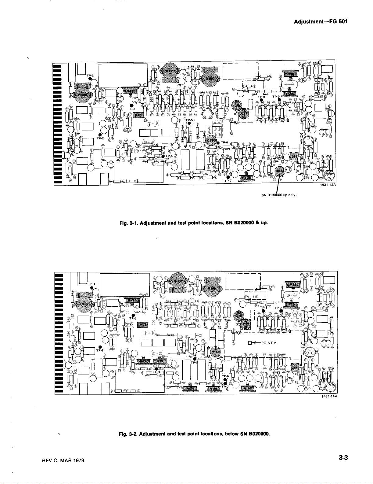
A
dj
ustment-
FG501
Fig.3-1.A
stmentand
dju
testpoint
locations,
SN Β
020000&up
.
Α
1431-14
REV
.Adju
Fig.
3-2
A
C,
M
R
1979
stmentand
testpoint
locations,below
SN Β
020000
.
3-3
Page 29
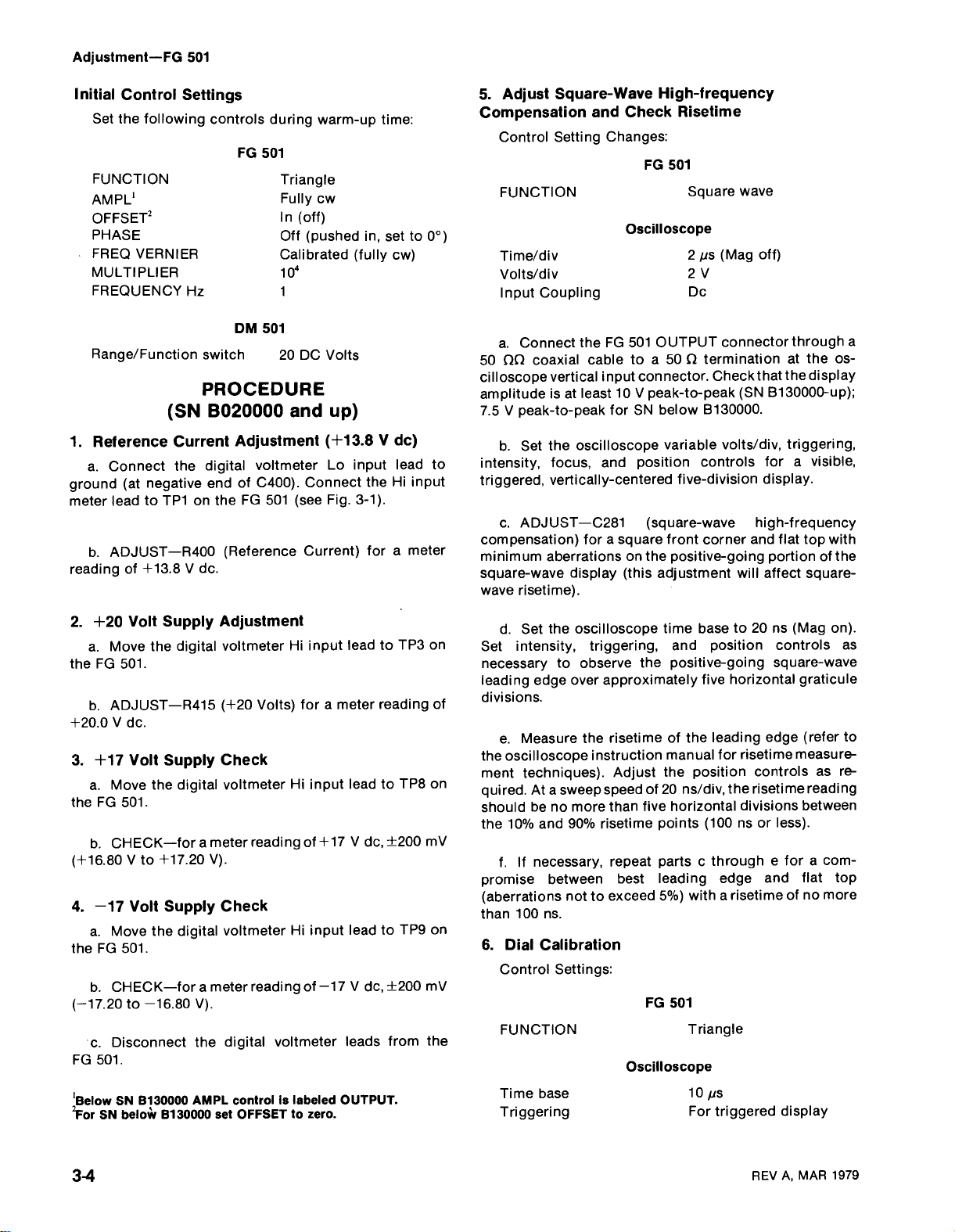
20
Adjustment-FG
Initial
Control
Setthe
FUN
CTIO
A
MPL'
OFFSE
PH
AS
E
FREQVERN
MULTIPLIER
FREQUEN
R
a
nge/Fu n
Settings
followingcon
N
T'
I
ER
CY
ction
(SNΒ
1
.Reference
α.Co
und
gro
meter
readingof+13.8V
(at
lead
b.ADJUST-R400(R
Current
nnectthedigital
negativeendofC400).Connectthe
ΤΡ
1onthe FG501
to
501
Hz
switc
PR
.
dc
trolsdu
F
G
501
D
M
501
h
OCED
020000
Adj
ustment
voltmeterLo
eference
ring
warm-up
Triangle
F
ully
εω
(off)
In
Off
(pushedin,
Calibrated(fully
10
°
1
DCVolts
time
URE
and
up)
(+13.8V
input
(seeFig.3-1)
Current)
.
forαmeter
:
setto0°)
cw)
dc)
lead
to
H
i
input
5.Adjust
CompensationandCheckRisetime
Control
FUN
Time/div
V
I
nputCoupling
α.Co
ΩΩ
50
cilloscopeverticalinputconnector.C
amplitudeisat
7.5V
b.Setthe
intensity,
triggered,
c.ADJUST-C281
com
mi n
imum
squ
are-wavedisplay(thisadju
wave
Square-WaveHigh-frequency
h
SettingC
CTIO
N
d
iv
olts/
nn
ectthe FG501OUTPUTconnectorth
coaxial
peak-to-
pensation)for
risetime)
p
oscilloscopevariable
focus,and
vertically-centeredfive-divisio
aberrationsont
.
anges
F
G
Oscilloscope
cabletoα 50Ωtermination
V
least
eakforSNbelowΒ130000
peak-to-peak (S
10
positioncontrols
(square-wave
αsqu
are
he p
:
501
S
quare
2μs(Mag
2
V
Dc
hec
volts/div,
front
corner and
ositive-goingportionofthe
stment
wave
off)
roug
t
heos-
at
kthatthedisplay
N Β
130000-υρ)
.
triggering,
α
visible,
for
ndisplay
h
will
.
igh-frequency
flattop
affect
squ
h α
wit
are-
;
h
2.+20Volt
M
α
.
theFG501
b
.
ADJUST-R415
+20.0Vdc
3.+17
α
.Movethe
the FG501
b
.
CHECK-forα
(+16
.80Vto
4.-17Volt
α
.Moveth
t
he FG501
b
.
CHECK-forαmeterreading
(-17
.20to-16
c.Disconnectthe
FG501
'Below S
Nb
'For
S
SupplyAdj
ovethedigital
.
.
V
olt
.
.
.
N Β
130000AMPL
elow'Β130000
lyCheck
Su
p
p
digital
+17
.20
SupplyCh
edigital
.80
V)
ustment
voltmeterHi
(+20Volts)
voltmeterHiinput
meter
readingof
V)
.
k
ec
voltmeter Hiinput
.
d
igital
ntrolis labeledOUTPUT
co
setOFFSETtozero.
input
forαmeter
of-17Vdc,
voltmeter
leadto
leadtoΤΡ8
V
dc,
+17
leadtoΤΡ9on
leads
ΤΡ
3
reading
±200mV
±200mV
fromth
.
on
on
of
Setthe
d
.
Setinten
necessary
leadi
ng edge
divisions.
M
e
.
t
heoscilloscope
ment
tec
d.At α
q
uire
sh
oul
d benomorethan
t
he 10ο/οand90
f.If
romisebetweenb
p
(aberrations
t
han 100ns
6.Dial Calibration
Control
e
FUN
Timebase
Triggering
oscilloscopetime
sity,
triggering,and
to
observeth
over
approximately
easurethe
hn
iques).Adjustthe
sweepsp
necessary,
.
Settings
CTIO
risetimeofthelea
instructionmanual
eedof20
ο/ο
risetime
repeatpartscthro
est
nottoexceed5ο/ο)wit
:
N
Oscilloscope
baseto20ns(Mag
positio
epositive-goi
fivehorizontal
for
positioncon
ns/div,
n
fivehorizo
points
leading
F
G
501
taldivisio
(100nsorless)
edge
h α
Triangle
10μs
For
triggere
n con
n
gsquare-wave
i
ng edge
d
risetime
the
ug
risetimeofno
measure-
trols
isetime
r
ns b
heforα
andflattop
d disp
on)
as
trols
graticule
(refer
to
as
re-
reading
etwee
n
.
commore
lay
.
3-4
REVΑ,
AR
1979
M
Page 30
SettheFREQUEN
α
.
w
herethe frequencyofthedisplayedwaveform
10)
becomes
willbeα
(thereisnosignal
and
maximum
p
ositioncontroltomovethe d
thesweepcanbeviewed.
thepointwh
to
on
thed
needle-n
7.Χ.1Symmetry
Control
sq
uare-wave
going
eq
repeatedly
j
ustments
maximum
fewdegrees
below
.1).Forease
fre
q uency,
b.CHECK-thattheFREQUEN
erethe
increase
c
t
he brass
FUN
FREQUEN
α.Setthe
b
ualdur
.
Ifthedialdoes
.
collarbehindth
ialto10wh
osepliers
CTIO
.
ADJUST-R45(Χ.1Symmetry)sot
and
ation.Switchthe
ileholdingthe potentiometer shaft
Settings
N
CYHz
oscilloscopetodisplayone
cycle
negative-goi
from
toR45
.
CYHz d
andthereisnotfurtherchange.
beforethewaveform
output
usethe
freque
not read10,
.Re-tighte
Adjustment
:
F
over10
ngportions
plus
to
ial
justtothepoint(near
forαpart ofthe area
in
determining
oscilloscopehorizontal
isplaysothat
CY
Hz
ncyoft
G
minuswh
he outp
loosenthetwo
edialandpanel;thenpositio
nthe
setscrews
501
S
quare
wave
N
ear
1
graticule divisions
ofthe
oscillosco
e
p
ilemak
disappears
above
point
the
right
the
rea
dial
utsignal
h
triggering
ds 10
setscrews
.
full
triggere
.
atth
epositive-
signal
ingfinalad
T
h
endof
ceases
wit
are
slope
10
of
of
at
α.Connectthe FG501 output
cable a
waveformisalsotobe
is
α tee
inputstothecounterand
10,000
cycle perdivision)
9.Χ1Calibration
n
h
d
and50
inputsofthe
tor
1
sion)
oscillosco
nd 50Ωte
connector
Time
base
Triggering
b.ADJUST-R20(Χ10Cal)
(an
Control
FREQUEN
Time
base
α.Connect
Ω
.
b.ADJUST-1338
.0000(noteanoscillosco
.
c.Setth
mi n
ationtothecounterinput
r
displayedonan
betwee
nthe50Ω
oscilloscope)
Oscillosco
oscilloscope
.
Settings
CY
Hz
(useofan
i
nthisstep
t
heFG501th
terminationtoα tee
n
terand
cou
e FG501
pe time
base
display
:
F
G
Oscilloscope
oscilloscope
oscilloscopetot
Χ
1
(
Cal)
pedisplay
FREQUEN
.1ms.
to
501
ustment-FG
Ad
j
ughα 50Ωcoaxial
thro
oscilloscope,in
terminatio
.
pe
.1
ms
Set
for
stable,
d
d
triggere
forαcounter
of
1
optional)
is
1
ms
roug
h α 50Ωcoaxial
connector.Connectth
α
for
CY
isplay
readingof
approximately
he tee connec-
counter
a
of
H
z
reading
bout1cycle/divi-
dialto10
n an
andthe
(ifth
sert
d
t
one
cable
501
h
of
e
e
e
c.Disconnectthe 50Ωtermination
cilloscopei
8
.Χ10
Control
MULTIPLIER
FREQUEN
FUN
Fun
H
Source
TriggerLevel
REVΑ,MAR
Calibration
Useof an
Setti
CTIO
ction
old
nputconnector
oscilloscopeinthis
ngs
:
F
CY
Hz
N
Counte
1979
.
N
G
ote
501
10'
10
Triangle
r
1
Hz
F
ully
E
xt
0
fromthe
stepisoptional
waveform
ccw
os-
.
d.CHECK
n
eceasary,re-adjustR20
(
note an
e
.Repeat
10.105Timing
Control
MULTIPLIER
FREQUEN
Time
F
unctio
-for
oscilloscopedisplayofabout1cycle/
Steps
8and
Adj
Setti
ngs
:
CY
Hz
(useofan
inthisstepiso
base
n
α
counter
(Χ10
9 asnecessary
ustment
F
G
501
Oscilloscope
oscillosco
Counter
reading
Cal) fo
10
5
10
tional)
p
1μs
.1kHz
rα10
pe
10
.000.If
of
.000
readi
ng
ivision)
3-
.
5
d
.
Page 31

ustment-FG
A
dj
α.AD
reading
Control
FREQUEN
Time
α.AD
reading
cycle/
12.10
only)
Control
ivision)
d
d
cycle/
11.105Χ
501
ST-C190
JU
1
.0000(noteanoscillosco
of
.
TimingA
1
Settings
CY
base
ST-C79
JU
.1000(note an
of
ivision)
°X10
Timing
Setti
.
ngs
Hz
(use
i
nth
:
:
(105Χ
ustment
dj
F
G
Oscilloscpe
an
of
stepis
is
(10
5
oscillosco
ustment(B
Adj
Timi ng)forαcounter
10
p
e d
isplayofabout
501
1
oscilloscope
optional)
10μs
Χ1Timin
g) fo
pedisplay
elow
SNΒ
r
α
counter
of
about
060000
1
1
F
G
501
FRE-
Q
UEN
CY
10
10
10
5
d
.
Setthe
MULTIPLIER
FINPUTcon
the
VC
squ
tion
input of
one
divisions
repeatedly
symmetry
Symmet
wave
are
e.Disconnectth
fromthe
oscilloscope.
an
triggeredsquare-wave
full
Switc
.
from
If itisno
.
ryAdj
Table
F
501
G
MUL
TI-
PLIER
10
10
3
10'
10
FREQUEN
switchto103.Place
.
distortio
htheoscillosco
plustomi nus and
ustment
CYHz
nector
e
SettheFUN
.
FG501
OUTPUT
n an
alyzer
Set
symmetrical,
longe
r
(Step 7ofthispr
3-2
FRE-
UEN
CY
Q
100
Hz
10kHz
kHz
100
5kHz
d
ial
for.1a
α 50Ωtermi
CTIO
cable
conn
pe
triggering
ectthemto
ocedure)
and
oscilloscopetodis
the
cycle over
checkthes
PERCEN
DISTOR-
ΤΙΟΝ
0.5ο/ο
0
.5%
1
.0%
0
.5%
atio
n
N
switchto
andterm!
graticule
10
uare-wave
q
repeat
ο
ο
nd
n
slo
theΧ
.
p
T
t
nat
he
on
he
lay
pe
.1
F
G
MULTIPLIER
FREQUEN
α.AD
(noteanoscillosco
.1000
n).
sio
13.Sine-waveUpperand
Control
JU
CYHz
ST-C77
Setti
ngs
:
(10"
Timing)
p
F
CTIO
FUN
MULTIPLIER
FREQUEN
A
MPL'
PHAS
O
FFSET'
α.ConnecttheFG
t
h
roug
b.AD
L
evel
DistortionAnalyzer.
the
c.C
Table
'BelowSNβ
'For
SN b
N
CY
Hz
E
h α 50
dj
a
heckth
3-2
elow
coaxialcablean d 50
Ω
ST-UpperLevelAdj
JU
ustmentR170
e
distortio
.
A
130000
8130000
501 totheDistortion
for
MPL
controlislab
setOFFSETto
501
10
°
10
foracounter
edisplayofabout
L
owerLevelAdj
G
501
Sine-wave
10
10
(100
Hz)
Clockwise
Ιπ
(off)
In
(off)
Ω
termination.
ustmentR150and
minimum
natt
distortio
he frequencies
eledO
zero
.
reading
1
cycle/divi-
ustment
Analyze
n as
TPUT
U
of
L
owe
readby
listedin
.
g.R
epeat
14.Triangle
Adjustment
Control
FUN
CTIO
MUL
TI
UEN
FRE
Q
P
erio
d
Duration
Amplitu
Time
r
50Ωcoaxial
GAT
r
tria
bursttothenext.R
base
Connectth
α
.
EINPU
PulltheFG501
b
.
c.CHECK-thatt
ngle
waveforms
Step
DC
Setting:
N
PLIER
CYHz
de
cable
connector.
T
13
parts
ε andd as
L
evel
and
Ph
FG501
Triangle
10
10
n
P
ulse
Oscilloscope
e pulse
and50Ω
PH
he
h αhorizontalbar
wit
erator
Ge
.2
.1
+2Vinto
.1
generator
termination
ASEcontrol
displayisseveral
otatethePHASEco
ase
°
ms
ms
ms
necessary
R
an
50
outputthr
+
out
connecti
.
ge
Ω
oug
totheFG
(on)
.
u
rsts
b
ngone
n
trol
h α
501
of
fully
3-
6
REVΑ,MAR
1979
Page 32

A
djustment-FG
501
clockwise
thetopofthe
control
should
waveforms
d.ADJUST-13135
n
ot
movement
e
f
g.Disconnect
pulse
15.Adjust
Control
A
OFFSET
V
α.Center
b.ADJUST-output
traceiscenteredonthe
c.Disconnect
This
andthehorizontal
triangle
fully
counterclockwise
move
toatleast
.
asdescribedin Step 14
ofbar
above
.Repeatpartscanddabove
.
R
eturnthe
generator
MPL'
olts/div
completes
PHASE
the cable
andFG
OutputBalance
Settings
2
:
the
oscilloscope
all
theFG
Oscilloscope
test
PR
(S
N
BELOW
Steps1through4:
forSNB020000-up
Adjust
5
.
Control
MULTIPLIER
V
Vertical
Triggering
TimeBase
Intensity,Level
&Position
'BelowSNΒ
2
ForSNbelowΒ130000
+4.5V
Setting
olts/Div
Input
130000
perform
onpage
olts
Changes
Oscilloscope
Coupling
A
MPL
set
bars should
burst
waveforms.R
and
the
bottomofthe
(triangle
andbelow
501
F
balance
screenofthe
OCED
Triangle
F
controlIslabeled
OFFSETtozero
DCLevel)ifoperation
partcabove
asnecessary
knobto0°
and
GATEINPUT
(SNΒ130000
G
501
M
inimum Output
Ιη
(off)
.1
V
trace
controlR274until
equip
ment
501
adjustment
URE
Β
020000)
Steps1through4as
3-4 except
Amplitude
:
G
501
10
1
0.2V
Dc
Auto
1
ms
For
visible,
movetoat
otate
the
thehorizontalbar
triangle
(adjust
the
burst
and
termination
.
oscilloscope
.
refer
O
.
for
waveforms)
.
pressitin
from
.
and
procedure
toFig.3-2
triggereddisplay
UTPUT
.
least
PHASE
burst
equal
(off)
up)
(ccw)
.
shown
.
the
the
α.Connect
point6(ifΤΡ6ίsnot
pad
below
clip
to chassis
b.Set
is
viewed
.
.
.
c.Set
anduse P
centerhorizontal graticule
dc
.
d
.
ADJUST-R195
ositive
p
the
graticule
e.ADJUST-R205
n
egativepeaksonthedisplay
graticule
f.R
epeat
6.Triangle
α
.Move
b.ADJUST-13135
extends
center
.
7.Gate
α
.Move
b
.
Use
the
graticule
c
.Move
CenteringR95)
d.ADJUST-R95
graticule
Disconnect
e
.
FG501
8.Square
α.Connectα50Ωcable
connector
vertical
b.Set
ε.Set
d.ADJUST-R99
display.Ifnecessary,
vertically
α10Χ
p
robe
from
present
C77
and
rightofR
ground
FREQUENCY
on
test
oscilloscope
oscilloscope
osition
control
p
eaks on
center
an
Centering
vertical p
.
and
input
OFFSET
FUNCTION
centered
thedisplay
.
center
.
partsdand
Level
DC
probe
tiptoΤΡ7(emitter of
equaldistance
the 10Χprobe
osition
.
the
probe
.
the
disconnect
W
ave
Amplitude
toα50Ωterminationatthe
connector
andOUTPUT
.
usepointΑ,
251).Connectprobe
.
Hz
for
maximum
.
vertical
tovertically
(+4.5volts,ι
(-4.5volts
(
tiptoΤΡ4(center
to
p
robe
probe
.
to
(
ηι
adjust
input
line.R
extend 2
extend2.25divisions
e asnecessary
DCLevel)sothe d
ti
above
tiptoΤΡ5(Q85
controltocenterthedisplay
re-center
tipand ground
from
from
for
(square
r
L
Ampl
OFFSET
the
oscilloscopetotest
t
he
circuit
frequency
couplingtoground
centerthetrace
eturn
input
coupling
Ampl)
.25divisions
Ampl)
ti
.
Q38)
.
and
below
base)
tapofGate
the
display
clip
oscilloscope
the FG501
α6division
wave)
Cal)
tokeep
OUTPUT
oscilloscope
.
forα6-division
board
ground
as
atthe
to
so the
above
so the
below
isplay
graticule
.
on
on the
from
the
.
display
.
display
REVΑ,MAR
1979
3-7
Page 33

dj
ustment-FG
A
S
quare-Wave
9
.
Control
Setting
501
Hig
C
han
h F
ges
requency
:
Compensatio
d
theup
wave
per
are
b
n
p
ortions
d
uration
.
ST-R45(Χ.1Sym)
AD
JU
t
he d
of
.
isplayed
so
square
lower
an
equal
of
ti
B
ase
Time
Triggering
JU
Calibration
n
trol
SettingCh
CTIO
ST-C281
corneronthe
N
α.AD
and
square
10.Dial
Co
FUN
FREQUEN
Time
base
α
.CHECK-t
n
ot,perform
L
oose
b
.
hin
be
p
lierstomaintain
rotating
11.X10
α
.
form/
nthe
d
t
heFREQUEN
dial
to
Calibration
ADJUST-R20
d
ivision
Oscilloscope
&Position
anges
Hz
CY
Oscillosco
hatthe
p
artb.
two
maximumfreq
read
10,thentig
.
(
91
dis
F
G
FREQUE
set
Hzknob
CY
(Χ10
2
AsRe
HF
lay
p
:
501
M
frequency
1
screws
Cal)
μ
s
uire
q
Comp)
.
(triangle
Ν
aximum
e
p
ms/divisio
NCY
Hzdial
on
dR25 sh
.Hol
ue
ncydisplay
h
ten
screws
for
1
d
for
best
waveform)
dis
p
n
the
brass
.
triangle
flat
layed
reads
aft
top
10;if
collar
wit
while
wave-
14.105Χ
Control
FUN
MULTIPLIER
FREQUEN
Time
α
.
waveform/division
105X1
15
.
α.Set
b
ase
b
.
waveform/division
b
est
for
h
16.104Χ10Timing
α.Set
oscilloscope
b.ADJUST-C77
waveform/divisio
Timing
10
SettingChan
CTIO
N
CY
base
ADJUST-C190
Timing
FREQUEN
d
for10μ
s/
ivision
ADJUST-C79
calibration
TIPLIERto104
MUL
time
ges
F
G
Hz
Oscilloscope
(105Χ10Timi n
.
CYHzto1
.
(105Χ1Timing)
Repeat
.
.
for10μ
base
(104Χ
n
.
:
501
10
10
1
steps
FREQUEN
,
s/division
10
(triangle)
5
s/division
μ
for
g)
and
oscilloscope
forone
14 and 15 as
CY
.
Timing)
for
one
triangle
tria
necessary
Hz
to
triangle
one
time
n
gle
10,and
ti
12.Χ
base
form/
Calibration
1
Set
.
FREQUEN
α
for10ms/divisio
ADJUST-1138
b
.
ivision
d
c.Set
for1ms/divisio
base
d.CHEC
readjustR20
calibration.
13.Χ
Symmetry
1
α.Set
uare-wave).Set
(s
q
sion
.
3-8
.
FREQUEN
K
-for
one
andrepeat
MULTIPLIER
oscilloscopetime b
H
CY
n
.
Χ1Cal)
(
H
CY
n
.
triangle
to
z to1and
for
zto10 a
nd
waveform/divisio
arts
αthroug
p
10'and
oscilloscope
triangle
one
oscilloscope
h
FUN
CTIO
ase
for10ms/divi-
wave-
n.Ifnot,
d
for
Ntoηι
time
time
best
ε.Discon
cilloscope
17
.Upperand
Control
FUN
input
SettingC
CTIO
MULTIPLIER
FREQUEN
n
α.Co
nectthe50Ω
thedistortion
ADJUST-
b
.
L
owerLevel)
analyzer
.
n
ectthe50
.
L
ower
han
N
H
z
CY
analyzerinpu
R
150(`1
forαmin
Ω
terminationfrom
W
ave
Sine-
ges
F
G
:
501
Level
(sine
104
1
terminationonOU
t
.
L
ι
imum
U
evel)
pper
distortionreading
wave)
TPUT
andR170
@MAR1979
theos-
cable
`1
(
t
he
on
to
ι
Page 34

M
AI
N
TEN
A
N
C
E
A
N
D
Sectio
n4-F
501
G
EVEN
P
R
P
reventive
basis
will
en
checks
malfunction
maintenance
forming preve
adjustment
Cleaning
Donot
carbon
alcohol,
Fr
clean
the
of
.
use
compounds
eon
waterandαmil
I
NT
TI
n
tenance
mai
h
ance
the
semiconductors
r
e not
a
measures.Therecomme
tive
maintenance
n
acetone,
hlor
tetrac
methylenech
ERF
VE
MAINTEN
steps
reliability
recomme
ΜΕΚ,ΜΙΒΚ
ide,trich
loride,
cleaning
for
detergent
d
perfo
theFG
of
i
nth
nded
ustbefore
is
j
benzene,
,
loroet
sulphuric
t
h
eF
.
ACI
ANC
r
med
onαregula
501
e
absence
as
nded
time
h
ylene,
G
501.U
N
E
owever,
.
H
preve
for
umen
instr
toluene,
methyl
acid,
only
se
G
of
ntive
per-
o
r
I
NF
r
Circuit
α
d
section
t
O
Descriptions
Section5
.Used
etail
ca
Diagrams
Α
bloc
locatedon
circuit
assigned
The
symbols
M
compone
may
aprons.Thoseportions
boards
diagrams
first
ajor
circuits
be shownwit
are
RM
T
ROUBLESH
of
n
be α powerful
k d
iagram
foldout
u
circ
page
and
n
tnumbers.Im
ATIO
t
his
manual
conjointly
anddetailed
pagesinthe
show
it
reference
the
Diagrams
of
referencedesignators
are
usually
hinth
d
enclose
withgray
OOTI
explains
wit
hth
analytic
the
numbers
ide
ortant
p
e
diagrams,
the
of
N
N
G
circuit
e
tool
circ
iagrams
d
p
onent
com
of
n
sectio
usedin
n
tifiableby
waveforms
circuits
outline
tint
AIDS
rcu
it
operationin
ci
diagrams,
.
it
diagrams
u
section.T
eachcompo
defines
and
or
on
locate
.
values
the
the
ma
α se
voltages
adjoining
d
on
the
are
h
a
nd
ent
n
circuit
n
ual
r
ies
of
circuit
e
.
.
E
xterior
.Loose
or
drybrush.Water
h
owever,
precede adjustment
the
compressedair
d
irt
swab,orα
d
etergent
Adjustment
describe
withi
more
instrumentasdirected
L
ubricatio
abrasive
Interior.Cleaning
settingsofcalibration
can
be
cot
.
After
cleani
d in
n
s
p
ecification,noa
of
the
lubricationisrequired
No
dust
cleaners shoul
sincet
blow
to
removed
h
d
ampened
n
gorrepairs,dotheperformance
Section2of
specificatio
n
may
be
removed
andα mild d
interiorofthe
the
h
ecleaning
adjustments
off
accumulateddust
withα
softdry brush,cotto
inα
solution
this
manual
ustment
dj
n
s are n
inSectio
i
nth
etergent
n
d
ever
process
.Use
.Ifall
isneeded.If
ot met,
n
3,
Adjustment
eFG
h
α
wit
maybe
be
used.
unit
low-velocity
.Har
water
of
functions
calibrate
501
.
soft clot
couldalter
used
should
den
ed
n
-tippe
andmil
checkas
are
one o
the
.
h
d
d
Cam
Cam
compre
;
switc
from
The
contactisclosed
Circuit
Line
withα
d
fol
relatedcircuit
shooti
t
h
e
ndord
a
P
arts
r
Com
sig
standards
informatio
follows
SwitchC
switches
h
hcon
the
charts
illustratio
grid
out
page
To
identify
n
g,
Diagrams
ering
list
p
onent
Colored
n
ify
electrical
the
h
arts
shownon
ensive
front,
B
charts
to
tactinthe
also
oardIllustrations
locator
andseque
turnto
.
stripes
Componentsnot
.
n
p
same
complete
b
orkno
diagrams
section.Com
data are
and
rinted
end,
indicate
.
n
s showing
and
electrical
appropriate P
the
givenin
Wi
ring
or
values,
on
ΕΙΑ
standar
table
nced
h
e
t
locate
switchassembly,
toward
withα
compo
are placedon
as
closely
.
ponen
com
p
onent
theR
Color
dots
on
tolerances,
color
d
t
h
e
bo
d
s
.
diagrams
the
cam
the
rear
d
dot
soli
n
ent
locationskeyed
as p
ts
artsLocatio
values,descri
eplaceable
es
Co
d
electrical
accordingtoΕΙΑ
etc
.
codedusually
y.Some
are
co
de
r
numbe
counting
of
the
switch.
wheneac
the
backof
b
letothe
ossi
trouble-
whe
n
n
E
lectrical
components
wiring
d
of
Gri
p
tions,
h
codi
on
the
din
ave
n
h
α
g
REV
Α
,
M
AR1979
Page 35

Main
tenanceand
InterfacingInfor
mation-FG
501
TestingEq
Gener
capacitance
to
performbasic
diagnosticpurp
formance checkp
necessary
TR
This
that
p
roceeding
Control
Incorrectcontrol
d
oes
fun
ctionor
instructionsin
Ifthe FG501isoperating
systemor
otherin
con
nections
modules.Chec
thatth
defective.Chec
uipment
ally,
α wi de-
probe,
and
waveform
oses.The
rocedure
to a
dequ
atelycheckouttheinstrument
O
UBLE
troubleshooting
check
Settings
not exist.Ifth
strumentsinthesetup.Check
ein
terconnectingcablesand
SH
s thesimple
to extensivetr
setti
ereisanyquestionaboutthe
operatio
test
betweenthepower
n of
Section1.
setup,alsocheckcontrol
kthatthe
kthepower
bandoscilloscope,
αmu
ltimeterare
andvoltagechecksfo
calibration p
list
specific test
OOTI
N
G
TE
procedureisarran
trouble
oubleshooting
ngs canind
any control,
as
partofan
moduleandtheplug-i
signalisp
source
rop
signalsourcearenot
.
α
all thatisneeded
rocedureand per-
equipmen
.
C
HN
IQUES
gedin
an
possibilities
.
icate
α
seethe
interconnected
settingsoft
forpro
erly
connectedand
before
trouble
correct
operati
erinter -
p
low-
orde
that
ng
h
I
ncor
rect
operatio
inpowersupp
correct
according
r
pr
p
owe
t
instruments
theseinstances, suspectedci r
conn
time to
V
oltagesand
r
waveformand
thecircuitdiagramorintheadjustmentp
waveformsand
will
Com
t
he effectsoft
when
tr
ansistors andi
compone
board
e
n
power
semicond
voltagesoftheindividual
tothecircuitdiagramsandadju
ocedures.T
rmodu
ectedfrom
Oftend
vary
pon
Ifαcomponent
evaluati ngth
.
Tra
les.Defective
can
narrowthe
efective
betweeninstruments
entChecking
nts
canbeun
n
sistors andIntegratedCircuits
switc
h
uctor
n of
all
lies
.Usingαmultimeter,ch
hen
chec
ktheunregualtedsuppliesoft
appear
apparen
W
aveforms
voltageind
voltage
cannotbedisconnected
heassociate
emeasurement.Exceptfor
n
offbeforeremovi
.
aspowersupplypr
tly
search.
componentscan
labels
tegrated
solderedand
circuits
compone
bad p
icatio
d circuitrymust beconsidere
ci rcu
often
meanstrouble
ec
regulateds
nts
elsewhereinthe
cuitssh
owersuppliesoneat
nsw
are
typ
.
its,one
ng or
ould be
be
located
hent
heyapp
rocedures.Suc
icalind
from
end
lifte
dfromth
(IC).Turnthe
replacingany
icatio
soldered-i
first
k
upp
stment
oblems.In
dis-
by usin
ear
ns and
its
circuit,
ofmost
ecircu
for
lies
he
α
g
on
h
d
n
it
Ifthep
anotherFG
Ifth
e
to
anot
ifthe troubleisconfi nedtoonecom
commo
V
isualCheck
R
broken
t
he
to
f
romoverheating
overheatingb
thenew
Circuit
N
otethe
w
hichthe
appearinmorethanonecircuit,ch
circuitsbymakingwaveformand
ower
module
501know
troublepersists
her
compartment i
n to
allofthem
emovethecovers
wires,
looseorun
circuitboard,
efore
component
Isolatio
symptom.It
trouble is
n tobegoodi
andthelike.Ifcompo
are found,determinethecause
r
eplacingthe
may
n
is
suspected,
ntot
aftersubstitution,
ηthe
powermoduletod
.
fromth
located.
e FG501and
solderedconnections,damage
component;
alsobed
oftenid
amaged
entifiesthecircuitin
When trouble
voltage
trysub
h
e
movetheFG501
ec
kthe
meas
stituti
power
module
etermi
p
artmentoris
loo
k for
nentsdamage
oth
erwise,
.
symptoms
affected
eme
ur
Α
goo
d chec
ng
manceund
.
effectively
forit(oronewhichhas
ne
H
owever,besurethatcircuit
replacement
stitute
tra
Static-ty
checkoperation u
wick-typedesoldering
soldered-intransistors
d
of
test
un
troubleshootingcircuits
Operating
informatio
circuitdescriptioninformatio
voltagesand waveforms
thatadj
means of
integratedcircuitsiswithanintegrated
n
ts
.
This
pe testers
Integrated
oscilloscope,
derstandingofthecircuit
acent
device
k of transistoroperationisactual
erop
erating cond
becheck
nsistors are not availab
waveforms,
n
for
clippingαtestprobetothe14-and16-pinin-line
also
edbysubstituting α newcompo
tran sistormight
are notrecommended
nder
circuits
or
t
heintegrate
leads
are
doub
itions.Α
bee
conditionsar
simulated
tool
.
be
can
b
y dir
u sing
logic
levels,
n
aro
undthe
not s
h
ortedtoget
lesasan
transistorcan most
nch
ecked
e nots
alsobe d
le,useαdynamic
can
checkedwith α voltmeter,
ect
descriptio
dcircu
.
U
extraction
amaged.Ifs
sincet
ope
r atingconditions.Α
beusedto,remove
substitu
se care
tion.Α
nisessential
integrated
and
otherop
itsar
e
whe
i
n
tegrated
her.Αconvenien
ci rcuit
tool
perfor-
previo
u
uchth
tester
heydonot
good
ci r
cuits
erating
n
inth
give
n checking
u
its
circ
test
.
nen
sly)
at
ub-
to
so
clip.
t
.
α
.
.
e
t
4-
2
REV Α
,MAR
1979
Page 36

Diodes.Donot
i
n
ternal
current.Hig
usethe R
h
s
termi
resista
lowwhent
tolerances
list
t
he
detected by chec
h
ighest
voltage
should
ope
tester,
P
X1000
nary
Ordi
orted
R
esisto
R
.
measuredvalue
Capacitors.Α
n
ARTS
signal
cond
itionby
n
als
.Wit
hthe o
nce shou
leadsare
he
rs.Check
are
esistorsdonot
scale
.Use anoh
ratingofthecapacitor
h
ighafter
be
capacitor
by checkingwhether
or
O
use
an
h currents
scale
on
diodes
measuringthe
mmeter
h
veryhig
ldbe
reversed
resistors
give
ninth
normally
varies
kyorshortedca
lea
k
ing
resistance
mmeter
initialcharge
canbestbe
RDERIN
h
mmeterth
o
may
damagethediode,
theohmmeter
maybe
settotheR
hin one d
wit
R
eplaceableElectrical
e
n
eedtoberep
widely
whichwillnot
.
detectedwit
it
AND
G
.
checkedforano
resistance
X1000
irection
.
ohmmeter.R
h
an
fromthe sp
p
hanohmmeteronthe
wit
Theresistance
thecapacitor.An
of
passesacsignals
REPL
athas
lace
ecified
acitor
excee
h αcap
ACI
αhig
so
or
pen
between
scale,the
andvery
esisto
P
arts
dun
less
value
can
be
dthe
n
readi
acitor
.
N
G
M
h
r
.
g
2.Inst
3.Αdescriptionoft
circuitnumber)
4.Tektronix
Please
ng d
receivi
Α
listingofTektronixField
andRepresentatives
ProductCatalogand
R
eplacing
Theexplo
R
eplaceable
themanual,
ing
or
assemblies
CircuitBoa
repair,
compone
aintenance
ument
r
do
irections
may
reassemblingi
.
entire
the
n
ts,can be replaced
andIn
SerialNumber
.
n
part
not
returnanyin
fromTek
Supplements
d
ed view drawings associate
M
ech
anicalParts
be
especially
rds.Ifα
assembly,
terfacing
h
epart
umber
can
nd
circuit
(for
(if
.
strume
tronix,
Offices,
be foun d
list,
h
elpfulwh
ivi
d
ual
boa
including
.
Information-FG501
example,Β010251)
electrical,include
ntsorpartsbefore
.
Inc
Service
inthe
.
locatedatthe
components
rdis
damage
Centers,
k
tronix
Te
d
withth
rear of
endisassembl-
or
dbeyo
soldered-on
all
.
the
e
sub-
nd
Ordering
n
dardP
Sta
b
eob
can
or representative
many
of
commercial
α p
order
pleasechec
rating,
replacement
physical
p
erformance
sh
ouldbe
ntcomponent
d
iffere
mentperforma
SpecialParts.Some
selecte
quirements,orare
specificatio
system
specialpartsdirectly
all
Officeorrepresen
OrderingProcedure.Wh
from
Tektronix,Inc
minimumin
1
.In
arts
tai
nedth
.
t
hesta
ndard
sourceinyour
art
fromαsource
ktheelectrical
tolerance,
parts,
size
and s
in
d
irect
nce
d byTektro
ns
.Mostofthemechanical
h
ave
beenman
formation:
ntType(FG
strume
electrical
.Most
h
your
roug
H
owever,
electronic
area
p
and
description.
itisimportanttoremember
h
apeofthe
anin
strument.All
replacements
will
not
.
p
n
ix,Inc.,to
manufactured
ufacture
fromthe
tative
.
en
leasein
.,
p
andmec
localTek
youshoul
compo
.
otherthanTek
arts
component
u
adversely
arts
dby
orderingrep
501)
tronix
d beabletoob
n
B
efore
listfor t
replacement
n
lessitisknownthatα
are
manufact
satisfy
forTek
tro
partsusedinth
Tektronix,Inc.Order
localTek
cludethe
.
anicalparts
h
field
ents
fromαlocal
you
purch
ase
n
ix,Inc.,
t r
o
he proper
Wh
en
selecting
thatth
may
affect
affectthe
particula
n
lacementparts
i
ured
ix,
Inc.,t
tronixFiel
following
office
tai
or
value,
its
parts
n
stru-
or
r
re-
οου
is
To
n
e
r
d
1.Disco
soldere
tions)
2
.Remove
or other
woul
d preventthe
instrument
3
.
bendtheboard
4.To
U
se carewh
place
TransistorsandIn
integrated
actually
routinemaintenance,
U
nnecessaryrep
devices
α
transistor
instrumen
the
remove
n
nect
d
lead
.
mounti
.
L
iftthe
replaceth
mis-alig
circuitssho
defective.If
may
is
lace
or re
connectionsand
screwsholdingthe
all
ng surface.R
circuitboard
.
replacingpin
en
n
ed,thepin
lacement
affect
replaced,
t that
αboard,
p
all
leads connecte
board
board, reversethe order
e
tegrate
l
d
u
removed
retur
calibrationofthein
the
checkthe operation
maybe
proceedas
dtotheboard
d
erlesspinconnec-
sol
boardto
emove
from
outoftheunit.Donot
connectors
d
n
otbere
nthemtoth
or
affected
anyknobs,
being
lifte
d out
connectors;if
maybe
Circuits.Transistors
placed u n
fromth
switchingofsemico
.
eir
socketsduri
eir
original
strument
ofthe p
less
follows
hech
t
etc
.,
ofth
forceor
removal
of
rced
fo
damaged
hey
t
sockets
nd
.When
:
(bot
assis
that
into
and
are
uctor
art
h
e
.
.
ng
.
of
REVΑ,MAR1979
4-3
Page 37

M
aintenanceandIn
Replacement
typeorαdirectrep
configurationofthe
ment
system.Whenremovi
α
suction-typede-soldering
theholes
An
16-pin integratedcircuits
This
P
artNo.
use
evenly
h
avi
the
Cam
undertake
Switch
be
carefully
F
or
or
representative
nth
i
extracting
toolisavailable
003-0619-00.If
caretoavoid
on bothends
ngon
e en
socket
beforetheotherend.
Switches.Repairof
n only by experienced
alignmentand
maintai
assistance,
terfacing
semico
lacement
semiconductors
e
circuit
toolsh
fromTek
damagi
of
d
theintegrated
of
spring tensionofthe
ned
co n
tact
.
ndu
boar
ould
an extracting
thei
for
your
Information-FG
ctorss h
ng soldered-intransistors,
tool to
d
beusedtoremovethe
to prevent
n
n
cam-type
proper
ouldbeoftheoriginal
.Figure
.
tronix,
g
t
tegrated
localTek
4-1showsthe
usedinthis
removethe
damage
Inc.Order
tool
hepins.Pull
circuit.Try
circuit
switches sh
maintenanceperso
operationof
tronixFieldOffice
501
solder
tothe
Tektronix
available,
isnot
slowlyand
disengage
contacts
the
to avoi
lead
instru-
use
from
14-and
pins
from
ouldbe
n
nel
must
switch.
4.To
removethe
block,
remove
the
switchand
of
block.Becareful
5.To
replacedefective
instructions
.
procedure
d
on
wires
sub-panel
.
Customizing
rear ofthemaincircuit
contactsandth
re-installtheswitchassembly,
6.To
.
Incan
descent
t
he sub-panelusingαplastic
and
pullthebulb
.
Input
an d outputaccesstot
camdrum
retainingringfromthesh
the
slidethe
nottolosethe
give
ninthe
B
ulbs.Th
t
heInterface
eir
respectiveΙ/Οassignments
camdrum
switchcontacts,
switchrepairkit
ePO
outofthe
heFG
board.Fig.4-2
fromthefro
outoft
smalldetent
.
reversetheabove
WER
light
bulbis
sleeve.Un
sleeve
fromtherear
501isavailableatt
n
tsup
aftonthe
he sup
roller
.
followthe
mounted
solder
the
ofthe
identifiesth
.
p
ort
front
port
lead
he
e
Α
cam-type
tools,
available
No.040-0541-00
Thecam-ty
whic
h areturnedbyfront-
leaf
contacts
contacts
switc
hescan
repair,
or replacement
1
.Using
metal switc
slippastthedetents
for
inspectionor
2.To
board,
first
t
he
andpullthelong sh
circuit
lingatt
co
up
3.R
emovethescrews
board)which h
switc
instructions,
from
pe switches
mounted
are
actuate
be d
bot
hth
h covers
cleaning
completely
remove
h
e potentiometer
ΝΟΤΕ
h r
ep
airkit
includingnecessa
an
d
r
ep
lacement
tronix,
Inc
Tek
.
consist
panelknobs,
on
d by
isassembledforin
follows
as
umbs,
pullthebottom
apart
far
and
come
.
remove
anyknobs
aft
outoftheswitchassembly
(fromtheopp
oldthecamdrumtothe
rder
.
O
ofrotatingcamdru
adjacent
lobes
on
:
enoughtowh
off.The
α
switchfromthe
or sh
aft
t
h
at
r
contacts
Tektronix,Part
and
setsofspri
circuit
boards.The
t
hecams.These
spectio
extensions.Loose
e
n,cleaning,
edgesoft
eretheywill
switchis
rear of
osite
now
open
circuit
theswitch,
.
sideoft
board
is
y
ms,
ng-
.
he
he
Α
power
availableth
w
hich
to
Also
possible
otherplug-inmodulesinmu
frames
Α
slot
i
den
tifies
family.If
corresponding
p
revent
i
nthatcompartment.Thisprotectsth
specialized
Consultthe B
module
REP
n
IftheTek
Tektronix
owing
sh
individualatyour
completein
he
servicereq
t
module
atprovidesαrear-panel,mu
Ι/Ο
lines
arein
.
between
theFG
i
n
the
terfaceiscustomized,
hert
han
ot
connectionsbe
uildingΑSystem
manual
mainframeop
can
behard-wired
tra-compartment
pins23and24onthe
501
as α
positionofthe
signalsourceplug-insfrom
for
further
ACKAGINGFORSHI
n
tronix
Service
:owner
strument
uired.
strument
i
Center
(wit
h address) a
firmthatcan
serialnumberandαdescriptio
ltiple-compartment
memberofthe
insert
power
made
tothatcompartment
sectionoft
information.
istobeshi
for
serviceorrepair,
ndth
be
n (Option
tio
lti-pinconnector
for
external
connections
rear
signal
α ba
modulejackto
eplug-i
PMEN
ename
contacted.Inclu
2)
access
main-
connector
source
r
rierinthe
bei
ngused
nshou
he p
ower
T
pped
to
attachatag
of
wit
n
is
.
h
ld
.
α
an
de
of
4-4
REVΑ,MAR1979
Page 38

Β
M
ai
nten
anceand
Interfacing
Informatio
n-FG501
ε
Ε
Β
~n
71
G
Ε
Ε
FE
T'S
Β~
M
Ε
~
ε
etal-Case
1
Ε
~
ε
P
lastic-Cased
Β
dTra
Β
ε
~
Ε
U
J
~UΕ
J
HE
ι
Β
Tran
sistors
Β
n
sisto
rs
P
ower
Transistors
14
W "
~
IntegratedCircuitsInd
Fig.4-1.Semiconducto
IntegratedCircu
r
d
evice
leadconfigurations
14
exi
ng
itsMounting
foundIn
t
h
eFG501
.
4-
5
Page 39

M
aintenan
andInterfacing
ce
TR
IGG
EROUTPUTCO
GATEINCOMM
TR
V
IGG
CFIN
FUN
EROUTPU
Information-
ASSIG
NMEN
CTIO
N
MMON
T
ON
GATEIN
COMMON
VC
F
IN
FG501
TS
CONTACT
25Β
24Β
23
22Β
21B
NMEN
ASSIG
N
TACT
CO
Β
TS
FUN
CTIO
N
ι
Save
and
wasshipped.
not
available,
Surrou
ndtheinst
protect
the
corrugate
h
avingin
a
nd
.Inpu
Fig.
4-2
ack
re-
usethe
Iftheoriginal
pack
re
r
finishofthe
d
cardboardofthecorrect
side
ageinwhichyour
p
packaging
agethe
ument
instrument
withpolyet
instrument.Obtai
dimensionsof
t/output
no
un
fit
is
as
follows
hylene s
carto
lesst
han
assignme
ntsatrearinterface con
instrument
for
useor
:
h
eetingto
nαcartonof
n
strengt
sixinches
1431-19
n
ector,rear
t
hantheinstrumentdime
more
instrumentby
tightly
or urethanefoam
si
des.Seal
stapler
The
ounds
carto
.
h
p
carton
.
n
test
view
.
n
k
ingthreeinchesofd
pac
betweencartonand
withshippingtape
strengthfor
yo urinstr
sions.
Cushio
u
instrument,onall
industrial
or
umentis
nthe
nn
age
200
Page 40

Section5-FG501
CIRC
Introduction
The
followi
ng
is
αdescriptionoftheelectrical
diagramandthe d
under
standingthisdescription
T
rian
gleWaveform
Operational
045Α/ΒandQ48A/Βare
voltage
emitters
(MUL
TIPLI
provi
d
econstantcu
toget
her
chargesthe
t
h roughC79)
constant
withU
48,
ch
argesthetimingcap
The
currentsou
t
hetimingcap
requirementsoftheamplifiers h
n
g
timi
currentsou
U
Q45Bsupp
CR
d
negativecurrent
example,ifCR100istur
goesth
positivedirection
passesthelin
R
com
theu
h
u n
pin10
U
output togopositive.Thus,pin9of
p
com
switc
negativedirection,
C R
currentsup
45
input(th
T
h
e
103
and
etermineswhetherthe positive
roughCR
190/
R
191andto
p
aratorsU195A/Β.The
pper
ysteresis
tiltherampatpin
goes p
80Cthen
aratorU195Bgoes p
p
aratorU195B.
h
085
101.Thus,th e
amplifiersU45andU48inconj
at pin3
wit
currenttotheemitters
current
.WithCR100
ofU45and U48isalso
of
Q45A/
ER)
and
rrenttotheemittersofQ45A/Βwhich
h
U
45,
composeαp
timing cap
.Resisto
composeαnegative
rces
acitorare
rces.045Αsu
e
remai
lieschargingcurrent
switch,
emitter-cou
sourcechargesthetimi
102tochargethe
atαlinear
ear
pins3and5of
h
ysteresis.The
ositive.Theoutput of
goes n
egative,whichcau
tur
n
son.The
whichturnsonCR100and
negativecurren
etailedsch
Generation
voltage
Β
andQ48A/Β.
resistancenetworkR53throug hR60
acito
r
networkR63
acitor
forthe
separate.T
ply.045ΑandQ45
pplies a
ing
n
currentgoestoground),wh
com
pled
ned
off,
r
m
p
a
voltageatpi
voltageatpin 6 setsthelower
off,
U
3reaches+1.77
ositive,whichen
Consequently,
collectorofQ85movesinth
followers.Thus,the
ositive
r
selectedby
throughR70 pr
of
Q48A/Βthat,
currentsourceth
selecte
d by
eratio
o
p
ave
little
ppr
to
the
posed
tra
nsistors
allthecurrent
timi
rate.E
mitter
t
h roug h d
upp
195Aisi
V
t
source
U
IT
ematic
oximately70ηΑ
ofCR100th
current
nth
sesnor
diagrams
.
L
OO
unctionwith
p
resentatt
Switc
currentsou
S50
.
n
p
al
am
hus,i
npu
effect
B areiden
timingca
085
ng
cap
f romQ45
ng cap
acitorinthe
follower
ividernetwor
er andlowerlevel
n 2 of
U195A
enegative
;
t
henthe
invertingamplifie
gateU80D
lower-level
ables
lower-level
emitter-coupled
ηοωchargest
D
P
GENER
h
S50
rceth
S50
(C72
ovid
toget
at
also
lifie
r
s a
t
current
upon
tical
pacitor.
roug
and
Q90,
sou
rceor
acitor.For
Q138
sets
state
output
com-
turns
onthe
he
,
at
es
her
nd
the
to
ile
h
B
k
at
r
e
off
he
E
SC
ci r
p
reversedbyinverti
changeatpin3
closely
source.Lowfrequencysymmetryisadjustablebypoten
tiometerR
applyi
withthevoltage
quently,thecurrenttothe
whichc
describedunder
RIP
cuitsinthe F
foldout
timingcap
linear
n
reaches-1.77V,theoutput
n
pin 13 ofU80D
on.CR101turnson
actionis rep
t
d
n
approximately10Vtopin 3 of
output
U
proximately
anyVCFinput applie
U
p
resistorsprovides
F
accomplis
1Hzto0.0001Hzbychanging
E
M
pagesatthe
ATO
rate.Again,theramp
etworkR
egative.This
h
e
Ιοορ
generator.Theslope(frequency) ofth
etermined
egativecurrentsourcesprovidetot
P
otentiometerR25
ofU30
15whereitis summedwithan
15hasanoutput
ositive
current
T
h
e
negativecu
ositive
voltageoutputofU15
tracksthat atpi
requency
F
requency(decade)switchingfrom1Hzto
xternalVoltage-ControlledFrequency(VCF)
ode
V
oltage-cont
ng
α
hangesthegenerato
TIO
G
501
.Refer tothesimplifie
N
bac
k
ofthemanualtoaid
d b
loc
R
acito
randtheramp
190/R191,andtop
causesthe
goes
negative,
again,wh
eated
to formαtriangle
by h
ow muchcu
(FREQUEN
is fedto
-7V)f rompotentiometerR38(Χ1Cal)
Χ
45
(
Switching
hed bychanging
voltage
pin2of
d to J10.Voltagesummingamplifier
rangeof+7to+17
source.This10V
α wide current(fr
rrent
ng
amplifierU40.Thus, the
ofU48inthen
n 3 of
.1
Sym)
.
r
olledfrequency
to J
10 (VCFINPUT)whichis
by
set
TriangleWaveformGeneration.
R
startstogonegativeatα
is
app
liedtot
in
5 ofU195B.Whentheramp
atpin10ofU195Bgoes
output
sou
25
ofU80Ctogo
Q85turns off,and
ileCR100
rrentth
CY
voltage followerU30.Th
voltagesummingamplifier
swingacrossthetimi
rceisalsodr
.However,the
egative
U45inthe
timingcap
timing resistors
(FREQUEN
timing
cap
routput
turnsoff.T
waveform
e p
hetiming
Hz)provides0V
offset
voltage
Vwhich dr
equency) range
ive
currentsource
positivecu
acitors,
is
accomplished by
CY
Hz)
acito
r
frequency as
k
in
he d
ivider
positive,
Q90t
urn
h
outputfrom
etrian
gle
ositiveand
capacitors
to
(ap-
and
ivesthe
ng
.
n byth
pola
rity
voltage
very
r rent
1
MHz
an
d
from
.
summe
.
Sub
se-
is
changed
s
is
is
.
e
e
is
-
is
d
,
REVΑ,MAR
1979
Page 41

Circuit
Descri
Shifting
L
evel
h
L
and
ensures
dropped
sine
the
(+7.5Vto-7
Sine
Thesi
associated
composed
voltage
series
R
163
turnonthe
CR
162
ramp
h
asthe
anode
clipped
reverseistrue of
Q170
tiometers
the
ofthe
from
ifting
evel
s
.
Q130isα
Q130
that
across
shaper
W
aveform
neshaperis
d
ofR155,R156,
divider
wit
hthe diodes
.Αpositive-goi
diode
DiodeCR
.
h successive
.
Eac
maximum
end.Th
h
arder
andits
R
150(Up
of
bases
sine
shaper
he
triangle
t
p
tion-FG
occurs
bias
any
R
127,which
r
cuit
ci
V)
.
.5
Generatio
ivider-dio
wit
h αdio
ngramp
wit
162
effect
hepeaksof
us,
t
t
han areth
the n
associated
per
Q150
and
output.Thus,
waveform
501
nthecircuit
i
current
hthe
source
across
(Q150
composed
denetwork.The
areresistors
has
diode
egative
Q170adju
source
h
iftsthelevel
s
ndQ170)
a
n
R
158,R160,
d
econnecte
from
leastcurrent
heleast
t
has α
sincethere
the
remaining
e
alfofthesin
h
divider-diode
evel)
an
stfor
α
.
d
sinewaveform
L
of
theemitter
composed
for
Q125
follower
of
withres
Q150,
Q170,
resistor
andR162
dtoeachj
R
157,R159,
first
;
effect
greater
triangle
R
thein
on
effect.C
isnoresistor
waveformar
portio
e
n
etwork.Poten-
170(L
ower
minimum
Q125
of
Q130
also
.
Q120
the
input
ectto0
p
and
an
n
etwo
forms
unction. Ι
R
161,
and
of
Q138
will
i
nthiscase,
comi
R
155
at
ns.T
shap
er,i.e
evel)
L
distortion
d
erived
is
is
to
V
rk
ng
its
he
α
η
e
.,
at
generator
p
i
n
In
J
215
0225
Q230
(composed
andQ242)
Q120.Assume
uare
s
q
p
ositive
conti
owever,when
H
off
1kΩ(R
to
of
U
Simultaneo
diodesCR245
Q120
associated c
Byadj
R
235
can
from
is
12
ofU80D
normal
(GAT
are
on
off.Wh
wave
transitionof
ues
n
becausethei
220
80D
is
is
now
ngtheinput
usti
(PHASE),th
sh
be
+900to-90°
functio
will
operatio
EINPUT),
(saturated),
n
Q230
e
U
235and
of
d
oes
not
that
isap
plied
to run,
pulledupa
u
ifted
si
t
he
nput
R
81),and
vs
sly,
Q230
throug
clam
rrent-boosting
u
e
to
fromthe
ing
.However,
n
d
isablethe loop
n
withno
transistors
hichholds
w
off,thephase
is
current
t
h
J
to
nd
tur
R
C
to
pin3of
to
S245
215
signal
d
turnsoff
t
248.T
e
he gate
ng
anceoft
he
loop
nson,wh
t
he voltage
transistors
triangle
sine
affect
switc
thegati
nce080
gating
impe
h
ped
clamping
startth
αpositive
generator
external
Q80
boosting
(PH
(GAT
signal,theloop
and
goes
he gate
U
voltagetot
and
gating
and
h
ase
p
clamping
transistors
of
source
E)isclosed
AS
EINPUT)
Q225
are
negative,
gating
he
and
Q80
generator
ichalso
of
setby
Q240
235
withpote
waveform
triangle
sourcefollowe
he gateofQ120
voltage
.
signal at
amplifier
gate
clam
p
follower
Duri
.
generator
alreadyon.
Q80
input
Q225
disabled.
is
turns
235and
U
d
an
n
tiometer
anyw
00sta
at
switc
circuit
Q240
andα
ngth
turns
d
rops
P
in
12
.
on
Q242
ere
h
point
rt
h
e
r
.
.
square
215
erature
p
W
riverQ90
pin12of
aveform
waveform
square
switchS250(FUN
to
Gate
(GAT
switchS250
si
or
.
at
theinpu
S
q
uare
Α
available
switchd
R
105and
External
Gatingisaccomplishedby
J
to
long as
Cam
sq
uare,
amplifier
Transistors
followersth
between
tem
waveform
and
ode
M
EINPU
nor
waveform
ne
Q250and
offset
com
p
Generation
t
ensation
output
feedingitthro
T)
gateU80Disnear
(
(via
andoutpu
fromthe
applying an
and
closing
FUN
CTION)
an d
Q255
R281 and
.
isderive
CTION)
feedsitto
are
compleme
Q276)
voltage
t
d bytakingt
collectorofcurrent
ugh d
ividerR102-
.
exte
rn
(PHASE).As
S245
ground,theloop
T
O
U
selectsαtria
t
n
tary
anydiffere
and
he
al
signal
PU
T
n
gle,
he output
emitter
n
tial
rovi
p
de
Hold
betweenthe
sto
level(i.e.,t
taneous
p
normally
A
MPL
(
t
tiometer
throug
operational
ode
M
switchS50
Cam
pthe
triangle
hetimingcap
level)until
osition.The
closed.
IFI
Assume
CTION).The
FUN
ositive
p
ut
R
260A (OUT
R
h
R
279and
he outp
resistor
rovidesth
p
α
(MUL
h
ree
lowestfreq
t
waveform
S50isswitc
h
old
contacts
ER
thatαtriangle
ngle
tria
amplifier
268.T
amplifier
epositive
voltage
is
PU
outputamp
he
.
feedbackresistor
i
nput.Now,
isapp
PLIER)hasthree
TI
uency
at
its
instanta
acitor
chargeholds
hedbacktoαrange
cam
on
waveform
rmvoltage
wavefo
varied
T),th
Its
in
summed
en
isdetermined
gai
n
lifier is
R281
w
hen
to
lied
its
settingsth
range
neousvoltage
switchS50
is
selected
amplitude
wit
.
Tra
Q270
Q290
base),
positions
at
at
its
instan-
are
b
y
S250
applied
by
poten-
t
hecurrent
h
basically
sistor
n
turnson(i.e.,
an
byinpu
0270
turnson
to
t
Page 42

w
htu
rnsonQ295and
h
ic
on(i.e.,Q270
to
its
Consequently,
R
298
establis
P
otentiometerR274provides
balance
P
ulse
Switch
ramp
waveformstothe
turnsoffwhen α
base),
andRamp
Q280
Q298
hesthe
.
S250
(FUN
ρυΙ
tur
ns on,wh
turnson
source
Generation
CTIO
output
Ist
he outputup.If
negative
and
impedance
N)
also
amplifier.
voltage
h
turns
ic
pullstheoutputdown.
ofth
adjustment
an
app
lies
Q276
turns
app
lied
is
on
Q285
e output
fordo
pulsesand
by
.
negative
selected
.
current
wouldincrease
theslopeof
trueift
heduty
t
d
tria
the
Wh
en αpositive
S250,αlower
current
ram
sourcehad
negative
he
ositive
P
erivedfromthe"on"
ngle generator
square
ornegative
cycleoft
waveform
or
resista
sources,
waveform
p
inthatsourceand
thatparticular
current
he sq
frequency
Circuit
egative
n
nceisswitc
dependingon
.For
the
least
sideoft
source
ulses
p
uare
waveform.T
p
ortion ofthe square
and,thus,thepulse
Description-
ramp
waveform
hedin
instance,
n
resista
consequentlyincrease
he
ramp.The
h
astheleast
are
obtainedby
determi
nesthefreque
F
G
is
selecte
the
positive or
to
t
he p
olarityoft
ifthepositive
ce,the n
he
current
reverse
resistance
ch
anging
outputpulse
waveform.T
freque
ncy
ncy
501
d
he
is
.
is
he
of
.
+20VR
Diode
theraw25Vacfromth
isthenfedtothe
transistor
current
temperature
potentiometerR400(R
7VacrossR405,whichthen
reference
N
egative
R
410-R415
for
sensing
transistor
of
+20VDecoupledSu
booster
power
Q424whenoutput
dow
Supply
-20
amplifierU480.Input
R
482
Supply
inthe
Q488,
provide
eference
The+20VSupplyisthe
bridgenetwor
Q400
source
for
feedbackis
.PotentiometerR415
+20Voutput.Wh
resistorR417inthe
0410
0410andsh
V
oltage
nthe
The-20VSupply
followerU420,
Q420,drives
module.C
baseofQ420
.
V R
eference
areO.1%,th
accurately
+20
current
overcurren
Supply
kCR
epower
+20VR
withR
along
for
compensatedata
non-inverting
turns
utsthe
V R
sensingresistor
V
6
.2
eference
providedthroug h
en outputcurrent
Q415
+20VSup
pply
theseries
rrent
u
ntexceeds
curre
andshuts
Supply
consistsofinverting
resistor
ereby
ensuri
followsthe+20
eference.Supply,
t shutdown(in
reference
400and
eference
zener
operational
on,which
inconjunctionwit
sensing
R481
ngthatthe-20
P
O
WER
thesupplies
for
all
C400
.Field
α co n
mAwh
adjuste
is
ds200
nthe
dow
hcu
turns
whic
V
Decoupled
operational
VR
pass
transistor
con
405
h
efere
mA)
capacitor
d
uleto+33Vdc,whic
mo
p
ply
Su
405
compose
diodeVR405.VR
pproximately 7
Current)isadjustedfor
establis
(+20Volts)
emitterofseriespass
p
pass
resistorR424
offth
V
R
487,and
hesthe 6.2V
amplifierU410
resistornetwor
excee
pulls
ly
off
.
transistorinthe
400 mA,
e+20
andfeedbackresistor
ReferenceSupply.As
series
transistor
excessof200
vert
h
effect
stant
is
en
d
mA,
base
n
rre
on
pulls
nce
0485
.
UPPL
S
-20VDecou
V
.
.
k
t
oltage
booster
identicallytothe+20
+17VSup
V
oltage
compose
tablishes
su
pplie
current
voltage
R
eference Supply,which h
-17VSu
The-17VSupply
amplifier
R
464
and
respect
+5VSu
DividerR441-R442
followerU440.If
sensingresistor
b
aseofcurrent
Su
pply
+11.5V
-5VSu
The-5VSu
current
current
des
p
rovi
IES
ledSupply
p
470
follower
Q472
and
current
ly
p
followerU430
the+17VSu
+17Vatpin3ofU430,
dtopin2from
sensing
forthe17VSupply
U
to
resistorint
pp
ly
460,
currentbooster
R
465which p
the+17VSupply
pply
excessive
R
446
b
ooster
Thecol
.
lector of
fromthe P
owerModule
pply
ply
p
limitingis
limited-20VR
temperature
providedsincethecollector
withits
U
sensi
V
DecoupledSup
withvoltage
pply.Divi
current
as
consistsofinverting
rovide
.
p
rovides+5Vtopin3
turnson
Q445
Q445
consistsofemitter
eferenceSup
compensatio
associate
ngresistorR473
d
derR
while
booster
he
issupp
overcurrentprotection.
currentisdrawn,
Q447which p
connects
Q430.T
17VSupplysince
liedbythe+20
Q468
and 0.1ο
an accurate
andshuts
to
.
ply.DiodeCR
n
for
d current
operate
ply
.
ividerR430/R431
430-R431
feedbackis
hereisno
operational
resistors
/ο
-17Vwit
voltage
of
current
ulls
dow
offthe+5V
the
unregulated
istiedtothe
Q450
0450
.
follower
es-
the
nthe
.
No
450
V
h
5-3
Page 43

There
OPTIONS
arenooptions
for
theFG501atthis
time
.
Page 44

n
Sectio
7-FG
501
REPL
ELE
P
A
R
TS
Re
p
lacementpartsareavailable
orrepr
esentative
ChangestoTektronixinstrumentsar
mp
onentsasth
co
improvementsdevelo
r
i
orde
ngparts,
ty
peornumber
Ifαpart
Tektronix,
number.
Changein
.
eybecome
ped
in
i
n
to
clude
,ser
ial
youhave
Inc
.FieldOfficeorrep
formation,ifany,islocatedatth
our en
the
nu
mbe
ord
ere
S
PE
CIALNOTESAND
ΧΟΟΟ
ΟΟΧ
AC
EABLE
CT
R
ICA
L
ORDERINGINFO
fromorthroughyour
esom
eti
availa
b
le,and
to give
gineeringdep
followi
nginform
r,andmodificatio
d h
asbeenreplacedwithα n
resen
tative
Part
firstadded atth
Part
r
emovedafterthisserialnumber
artment.It isther
ationin
n
numberifapp
willcon
erearof thismanual.
.
PAR
RM
mesma
youtheben
you
tactyouconcerni
SY
is
se
TS
ATIO
localTektron
detoaccommod
efitofthelatest
rorder
:
Part
licable
ew
orimpr
MBOL
r
ial
numb
er
N
ix,
Inc
.FieldOffice
ateimpr
ove
circuit
eforeimportant,when
number,instrumen
.
ovedpart,your
ng
any
c
han
local
geinp
S
d
t
art
ITEM
NAME
In
,thePartsList,anItemNameisseparatedfromth
B
ecause
of space
further
ItemNameiden
u
tilizedwher
ACT
R
ASSY
CA
P CA
CER CER
CK
T
MP
CO
CO
NN
ELCTL
T
ELE
C
INCA
NDINCANDESCEN
LE
D
NONWIR
α
limitations,anIte
e p
ossible
.
ACTUATO
ASS
EMBL
P
ACITO
R
Y
AMIC
CI
R
IT
C
U
COMPOSITIO
CO
NNE
CTO
ELECTROL
ELECTR
LIG
NONWI
ICA
HTEMITTJNG
REWOUN
m Nam
emay
sometimesapp
tification,th
A
BBREV
e
U.S.
F
ederal
IATIO
PL
QTZ
R RECP
RE
RF
N
S
R S
YTIC
L
T
DIOD
E
D
SENS
VA
WW
X
XTA
e
d
esc
CatalogingHa
NS
STC
S
EL
EM
ICO
ND S
R
FMR
L
rip
tio
n byαcolon(:)
earasinco
ndbook
PL
ASTIC
A
R
Q
U
TZ
RE
CEPTAC
RE
SISTO
R
ADIO
FREQUEN
SELE
CTED
EM
ICO
NDU
SENSITI
VE
VARIA
BLE
WIREWOUN
T
RANS
FORMER
C
R
YSTA
L
mp
1-16-1
LE
R
D
CTO
lete
can
.Fo
CY
R
.
r
be
V
.ΣOCT.1975
RE
Page 45

Rep
laceable
E
lectricalParts-FG
501
Code
Mfr
.
00853
01121
02111
02735
04713
05091
05397
07910
24931
34553
56289
71450
71744 CHICAGO
72982
73138 BECKMANINSTRUMENTS,
74868
75042
80009
81483
84411
90201
91637
91836
SANGAMO ELECTRIC
ALLEN-BRADLEY
SP
RCA
MOTOROLA,
ΤRΙ
UNION
SYSTEMS
T
ELEDYNESEMI
SPEC
ΑΜΡΕRΕΧ ELECTRONICCORP.,
ϊ
P
S
CTS
ERIE
BUNKER-
TRW ELECTRONI
R
ESI
TEKTRONIX,
INTERNATIONAL
R
T
MALLORYCAPACITORCO.,
Ρ
DALEEL
KINGSELECTRO
Manufacture
L
ECTRO
WELE
.
ELECTRONICS
CORPORATION,
INC.,SEMI
ORDINATE
CAR
BIDE
V
ISIO
DI
CONNECTORCO.,INC
IAL
TY
RAGU
R
E
CTRICCO.
E
EL
CORP.
MINIAT
TECHNOLOGICAL
CORP.,THE
R
ΑΜΟ
STORS,
PHILADELPHIA
INC.
CTRONIC
.
M
ALLORYANDCO.,INC
ECTRONI
CORPORATION
CONDUCTO
C
NICSCO.,
CROSS
INDEX-
r
CO.,S.CAROLINADIV
COMPANY
CORPORATION
URE
R
CS,INC
CORPORATIO
SO
LIDSTATE
CONDUCTO
N
R
LAMPWORKS
PR
O
DU
INC
COMPONENTS,ΙRCFIX
EC
TIFIER
COMPONENTS,
.
DIVI
RPRO
-,MA
TERIALS
.
COMPONENTDIV.-35
T
S, INC.
C
HELIPOTDIV
.,
ΑΜΡΗΕΝΟLRFDIV
D
IVISIO
CORP.
TRW
DIV.OF
.
INC.
MFR.CODENUMBER
A
d
dress
.
Ρ Ο
BOX
12012ND
N
SIO
D.DIV.5005
ED
N
CAPACITORS
17070
N
ROUTE
343 SNY
11901MADISON
12515
3560MADISON
1142
4433RAVENSWOOD
644
.
2500
.
33Ε.
401Ν.BR
ΡΟBOX 500
9220SUN
112
3029
Ρ Ο
Ρ.Ο.BOX
40
ΕMCDOWELLRD,ΡOBOX
H
OFFMANAVE
W.B
W
W.FIRSTST
BOX
MAR
TOMA
128
STREE
EAST
GALEAVENUE
202
DER
AVENUE BERKELEY
CHADROΝAVE.
EARDSLEY
.
12TH5Τ
HARBORBLVD.
FRANKLINST
DST
OA
S
ET BLVD
ΕWAS
HINGTONSTR
372
609
BLED
ALE ROA
T
AVENUE
AVE
.
.
SOUT
.
AVE
.
.
.
.
D
NUFACT
H
AVE
.
.
EET
URER
20923
State,
SC
WI
AZ
H
EIGH
OH
C
NY
IL
16512
NE
NY
Zip
29671
53204
NY
85036
TS,NJ
44101
A
90250
IN
11787
MA
46514
60640
92634
06810
PA
CA
69153
68601
10707
Y,CA
08876
01247
90069
City,
PI
CKENS,
MILWAU
KEE,
CITY
OFINDUSTR
SOMERVILLE,
PHOENIX,
C
LEVELAND,
HAWTHORNE,
I
ND
IANAPOLIS,
HAPPAUGE,
NORTH
ADAMS,
ELKHARΤ,IN
CHICAGO,
PA
ERIE,
FULLERTON,CA
D
AN
BURY,CT
PHILADELPHIA,
ΒΕΑVΕΑΤΟΝ,OR97077
L
OSANGELES,
OGA
LLALA,
I
NDI
ANAPOLIS, IN
COLUMBUS,NE
T
U
CKAHOE,
91745
07922
46227
19108
46206
α
LY
REV.
ΙJU
1978
Page 46
CktNo.
Α
1
Α
1
Α
1
Α
2
Α
2
C34
C40
C72
C73
C74}
ς75Ι
C76
C72
C73
C74
C75
C76
C77
C77
C78
C79
C80
C85
C85
C89
C95
C120
C130
C150
C162
C170
C190
C191
C191
C196
C204
C211
C235
C242
C250
C250
C251
C255
C255
'
C271
C279
C281
C281
C286
C291
C294
C297
C400
l
indiv
lette
s
uffi
b
ly
EXAMPLE
1
j
ι
1
.
670-2105-00
670-2105-01
670-2105-02
670-2248-00
670-2248-01
290-0519-00
290-0517-00
295-0126-00
295-0164-00
281-0167-00
281-0513-00
281-0540-00
281-0092-00
283-0003-00
290-0527-00
290-0536-00
290-0534-00
290-0512-00
283-0003-00
283-0003-00
290-0572-00
281-0519-00
290-0572-00
281-0092-00
281-0629-00
281-0511-00
283-0001-00
283-0001-00
283-0067-00
283-0177-00
290-0517-00
281-0651-00
281-0511-00
283-0637-00
290-0529-00
290-0719-00
283-0178-00
281-0627-00
281-0151-00
281-0178-00
281-0523-00
281-0523-00
290-0517-00
290-0517-00
290-0324-00
i
dua
r s
uff
x and
:
Tektronix
P
artNo.
ti
m
in
l
and
ix
the
Serial/Model
E
Χ
ΧΒ
ΧΒ
ΧΒ
ΧΒ
ΧΒ
ΧΒ
ΧΒ
ΧΒ
g
capacitors
tolerance
tolerance
No
.
n
ff
Β
010100
8125503
Β
130000
Β
010100
Β
130000
Β
010100Β119999
Β
120000 CAP.,SET,MTC
Β
010100
8125503
060000
090000
Β
060000
130000
Β
010100
Η
020000
060000
110000
020000
Β
010100Β059999
Β
060000
Β
010100Η129999ΧCA
060000
Β
110000
010100Β129999ΧC
Β
Β
010100
Β
010204
130000
in t
prin
shouldbethe
t
Dsco
8125502
Β
129999
Β
129999
Β
059999ΧCA
8089999
8019999
8059999ΧCAP.,FXD,C
8129999ΧCAP.,FXD,C
109999
Β
Β
010203
hi
ted
CKTBOARDASSY
C
KTBOARD
CKT
CKT
CKT
0AP.,FXD,ELC
0AP.,FXD,ELC
P
CA
P
CAP.,FXD,C
CA
P
CAP.,VA
CAP.,FX
CAP.,FXD,ELC
CAP.,FXD,ELC
CA
P .,FXD,ELCTLT
CAP.,
CAP.,
C
AP
0A
P.,FXD,ELCTLT
P.,FXD,CER DI
CA
C
AP .,FXD,ELCTLT
CA
P
P.,FXD,CER DI
CA
CAP.,FX
CAP.,FX
CAP.,FXD,C
AP.,FXD,ELCTLT :6.8UF
0
P.,FXD,CER DI
CA
CAP.,FXD,C
P
CAP.,FXD,ELC
CAP.,FXD,ELC
CAP.,FXD,C
AP
CA
P.,
CA
P
P.,FXD ,C
CA
CA
P.,FXD,CER DI:l00PF
0A
P.,FXD,ELCTLT
CA
P.,FXD,ELCTLT
CA
P.,FXD,ELCTLT
s
assemblymust
on
t
h
same
e t
imin
f
285-
BOARD
HOAR
BOARDASSY
.SET,MTCHD:10,1,0
.,VAR,CER
.,FXD,CER
FXD,ELCTLT
FXD
.,FXD,CER DI
.,VAR,CER DI
.,FXD,MICA D
.,FXD ,C
VAR,CER DI
.,VAR,PL
g
o
r
all
ΧΧΧΧ-ΧΧ
N
ame&Description
AIN
:M
A
SSY
:M
AIN
A
SSY
:M
D A
R,CERDI
D,CERDI
,C
D,CERDI
D,CERDI
capacitorto bereplaced
AIN
SSY
:FUNCTIO
:FUNCTIO
TLT:l00UF
TLT
:6.8UF
HD
:
1
0,0
DI
:9-45PF,200
ER
DI
:27PF,+/-5.4PF,
DI
:51PF,
:9-35ΡΣ,200
:0.
01UF,
TLT
:15UF,208,20
1
0UF,20$,25
TLT
:
:lUF
:22UF,20+k,15
DI :O.OlUF
ER
:0.
01UF,
:O
.lUF,20$,5o
:47PF,+/-4
.lUF
:O
:9-35PF,200
:33PF,5$,600
ER DI
:22PF,+/-2.2PF,500
:0.
005UF,
005UF,
:0.
ER
DI
:0.
ER
ER DI
ER DI
ER DI
STC:1-3.5PF,
ER DI
be
o
001UF,10$,200
DI:lUF
:47PF,58,200
:22PF,
:20
PF ,2
TLT
:47
UF
TLT
:47UF,20
:O
.
lUF
PF
:1
:1-3
:
1
00
.8UF,20θ,35
:6
:6.8
:750UF,
ordered by
f t
h
e t
imin
N
N
,208,20
,208,35
.1,0.
01UF,995
.
5% ,500
+80
,20%,35
,
+80-20%,150
+80
,20$,SOV
,
+80
-208,25V
,20%,35
+/-2
.5%,l00
,20B,20
B
,
+80
,
+/-0
PF
,100
500
PF,
+/
,+/-20
,208,35
UF
+75
g
01UF,990
V
V
-208,150V
V
-208,150V
.7PF,
V
+100
+100
.2PF,
,25
-208,100
.25PF,500
V
V
-20
-10$,40V
the
capacito
F-
V
V
PF
MTCHD
PF
500
V
V
V
V
V
V
V
500
V
V
V
500
500
V
V
-0$,
-08,
V
V
V
V
500
V
V
V
V
V
PF,
500
V
,SOO
V
PF
V
V
9-digitpart
.The
rs in the
R
eplaceable
number,
lette
lectricalParts-FG
E
fr
M
Code
80009
80009
80009
80009
80009
90201TDC107M020W
56289
84411
80009
72982
72982
72982
72982
72982
90201TDC156M020
902
01 T
56289
56289
72982
72982
56289
72982
56289
72982
72982
72982
72982
72982
72982
72982
56289
72982
72982
00853D151E200D0
05397T368C476
56289
72982
72982
72982
34553
72982
72982
56289
56289
56289D46454
r
asse
m-
MfrP
art
Number
670-2105-00
670-2105-01
670-2105-02
670-2248-00
670-2248-01
LD
196D685X0035KA1
55-0005Α5
ΤΕΚ
295-0164-00
538-011301
301
538-011D9-35
855
D
-000P2G0270
-000U2JO5
-558Ζ5U-103
9-45
10
FL
M
025
DC106
196D105X0035HA1
196D226XO015
855
-558Ζ5U-103
855
-558Ζ5U-103
196D104X0050
308
-000COG0470
D
196
538-011
308
-000COG0330
301
-000COG0220
831
-559Ε502
-559Ε502
831
835
-515Β102
8131
196D685X0035KA1
374-00
301
-000COG0220
196D476X0025
8131Ν145
-OOOCOK0109C
301
518-600Α1-3
2222-809-05001
301
-000
301
-000
196D685X0035KA1
196D685XO035KA1
104X0050
D
9-35
Ν
039Ε105
1T2H047o
M
020A
Ε
U2
M
U2
M
FL
KA1
HA
H
Ρ
Ρ
Κ
TE
104
O101
O101
531
M
J
Ζ
Ζ
Ζ
I
K
AI
J
K
Ζ
J
K
Z
3
Ζ
M
M
REV.
7-
J
JUL
Y
1978
3
Page 47

R
eplaceableElect
r
icalParts-FG
501
CktNo.
C406
C415
C415
C455
C482
C485
C485
C490
C495
CR15
CR16
CR17
C
R
45
CR100
CR101
CR102
R
103
C
CR150
CR155
CR156
CR158
CR160
CR162
CR170
CR175
C
R
176
C
R
178
CR180
CR182
C
R
215
C
R
218
C
R
230
R
235
C
R
240
C
R
242
C
CR245
C
R
246
CR247
CR248
C
R
285
CR290
C
R
400
C
R
410
C
R
450
C
R
490
D
5495
J10
J80
J81
J215
J290
Tektronix
P
artNo.
290-0524-00
283-0000-00
290-0517-00
290-0531-00 CAP.,
283-0111-00 ΧΒ
283-0000-00
290-0517-00
290-0324-00
290-0531-00
152-0141-02
152-0141-02
152-0141-02
152-0141-02
152-0249-00
152-0249-00
152-0249-00
152-0249-00
152-0141-02
152-0141-02
152-0141-02
152-0141-02
152-0141-02
152-0141-02
152-0141-02
152-0141-02
152-0141-02
152-0141-02
152-0141-02
152-0141-02
152-0141-02
152-0141-02
152-0141-02
152-0141-02 ΧΒ
152-0141-02
152-0141-02
152-0141-02
152-0141-02
152-0141-02
152-0141-02
152-0141-02
152-0141-02
152-0488-00
152-0141-02 ΧΒ
152-0141-02
152-0488-00
150-0109-00
131-0955-00
131-0282-00
131-1003-00
131-0955-00
131-0679-00
Serial/ModelNo.
E
ff
Β
010100Β019999
Β
020000
125503
Β
010100Β019999
Β
020000
ΧΒ
130000
ΧΒ
130000
ΧΒ
130000
130000
ΧΒ
ΧΒ
020000
ΧΒ
020000
130000
130000
Β
010100
Dscont
Β
103149
0AP.,
CAP.,
CAP.,
P.,FXD,CERDI:O.lUF
CA
CAP.,
CAP.,
CAP.,FXD,ELCTLT
0AP.,FXD,E
S
EMICONDDEVICE:S
SEMICONDDEVICE:SILICON
SEMICONDDEVICE:SILICON
SEMI
SEMI
SEMI
S
EMICON
EMICONDDEVICE:SILICON,DIODE
S
SEMICONDDEVICE:SILICON
SEMICONDDEVICE:SILICON
SEMICOND DEVICE:S
SEMI
S
EMICON
SEMICO
SEMICON
SEMI
SEMICOND
S
EMICONDDEVICE:S
SEMICONDDEVICE:SILICON
SEMICOND
SEMI
S
EMI
S
EMI
SEMICONDDEVICE:S
SE
MICOND
SEMICONDDEVI
S
EMI
SEMICON
MI
SE
SEMI
SEMI
S
EMI
MI
SE
SEMICO
SEMI
S
EMICON
LAMP,IN
CONNEC
CON
CONNECTO
CONNECTOR,RCPT,:BNC,FEMALE,W/HARDWARE
CONNECTOR,RCPT
N
ame&Description
FXD,ELCTLT
FXD,CER
FXD,E
FXD,EL
FXD,CERDI:0.
FXD,E
CONDDEVICE:SILICON
CONDDEVICE:S
CONDDEVICE
D DEVICE:S
CONDDEVICE:S
D DEVICE:S
ND
D DEVICE:S
CON
D DEVICE:S
CON
D DEVICE:S
CON
D DEVICE:S
CON
D DEVICE
CON
DDE
D DEVICE:SILICON
CONDDEVICE:S
CON
D DEVICE:S
CON
D DEVICE
CON
D DEVICE
CONDDEVICE:SILICON
ND DEVICE:SILICON
CON
D DEVICE:S
D DEVICE:S
CAND:18
TOR
CTO
R,RCPT,
NE
R BODY,
:4 .7UF,20$,
:
DI
0.001
LCTLT:6
LCTLT:6.8UF,20iι,35
LCTLT:l00UF,208,1o
DEVICE:S
DEVICE:S
DEVICE:SILICON
DE
,RCPT,:BNC,F
.SUF,208,35
TLT:lOOUF
C
001UF,+100-0%,SOO
:750UF,
ILICON
ILICON,DIODE
ILICON,DIODE
:S
ILI
ILICON
ILI
ILI
ILICON
ILICON,30V,150M
ILICON
ILICON
ILICON
ILICON
ILICON
ILICON
:S
ILI
VICE:S
ILICON
CE:SILICON
VICE:S
ILICON
ILICON
ILICON
:SILICO
ILICON
:S
ILICON
ILICON
V
,26M
A
:FEEDT
:CKTCDΜΤ,3 PRON
, :BNC
V
lO
UF,+100
CON,DIODE
CO
CON,30V,150M
CO
W/HARDWAR
-0$,500
V
,20i
ι ,
lOV
,208,50
V
V
+75-10%,40V
V
,3oV,150M
,30V,150M
,3oV,150M
,30V,150M
,30V,150M
,30V,150MA
,30V,150M
N
,30V,150MA
,3oV,150M
,3oV,150M
,30V,150M
,30V,150M
,30V,150M
,30V,150M
,30V,150M
,150MA
,30
V
,30V,150M
N
,30V,150M
,30V,150M
,30V,150M
,30V,150MA 07910
,30V,150M
,30V,150M
,30V,150MA
N
,30V,150M
,30V,150M
,200V,1500M
,30V,150M
,3oV,150M
,200V,1500M
EMALE,W/HARDWAR
HRU
ν
V
A
A
A
A
ASSY
ASSY
ASSY
ASSY
A
A
A
A
A
A
A
A
A
A
A
A
A
A
A
A
A
A
A
A
A
A
A
E
G
E
Mfr
Code
90201 TDC475MO10E
72982
56289
90201 TDC107MOlOWLC
72982
72982
56289
56289D46454
90201TDC107
079101Ν
07910
07910
07910
80009
80009
80009
80009
07910
07910
07910
079101Ν
079101Ν
07910
079101Ν
07910
07910
079101Ν
079101Ν
079101Ν
079101Ν
079101Ν
079101Ν
079101Ν
079101Ν
07910
07910
07910
07910
07910
07910
80009
079101Ν
079101Ν
80009
71744CM
05091 31-279
74868
80009
05091 31-279
24931
MfrP
art
Number
831
-516Ε102
196D685XOO35KA1
8121-N
088Z5U104
831
-516Ε102
196D685X0035KA1
MOl
OWLC
4152
1Ν
4152
1Ν
4152
1Ν
4152
152-0249-00
152-0249-00
152-0249-00
152-0249-00
1Ν
4152
1Ν4152
1Ν
4152
4152
4152
1Ν
4152
4152
Ν
4152
1
Ν
4152
1
4152
4152
4152
4152
4152
4152
4152
4152
1Ν
4152
1Ν
4152
1Ν
4152
1Ν
4152
1Ν
4152
1Ν
4152
1Ν
4152
152-0488-00
4152
4152
152-0488-00
7220
ΜΒ
74300
131-1003-00
168-1
28
JR
L
Ρ
M
Ρ
R
V.G
E
JULY
1978
Page 48

R
eplaceable
Elect
r
icalParts-FG
501
Tektronix
C
k
tNo.
J
290
J
290
298
LR
Q45A,B151-0261-00
Q48A,B151-0232-00
Q80
Q85
Q90
Q120A,B151-1042-01
Q125
Q130
Q138
Q150
Q170
Q170
Q225
Q230
Q240
Q242
Q250
Q255
Q270
Q276
Q280
Q285
Q290
Q295
Q295
Q298
Q298
Q400
Q410
Q415
Q420
Q424
Q430
Q445
Q447
Q450
Q468
Q472
Q474
Q485
Q488
R10
R
11
R11
R13
R
15
R
18
R18
P
artNo.
131-0679-02
131-0274-00
108-0105-00 ΧΒ
151-0190-00
151-0192-00
151-0192-00
151-0192-00
151-0192-00
151-0302-00
151-0190-00
151-0188-00
151-0164-00
151-0192-00
151-0192-00
151-0190-00
151-0188-00
151-0190-00
151-0188-00
151-0190-00
151-0190-00
151-0188-00
151-0302-00
151-0133-00
151-0136-00
151-0439-00
151-0322-00
151-0440-00
151-1066-00
151-0311-01
151-0190-00
151-0190-00
151-0190-00
151-0190-00
151-0311-01
151-0190-00
151-0188-00
151-0188-00
151-0188-00
151-0188-00
151-0188-00
151-0335-00
321-0289-00
315-0102-00
321-0151-00
315-0332-00
321-0289-00
321-0272-00
315-0822-00
Serial/Model
E
ff
Β
103150
Β
125503
030000Β129999ΧCO
Β
010100
Β
060000
Β
010100Β129999
Β
130000
Β
010100Β129999
Β
130000
Β
010100Η129999
Η
130000
Β
010100Β069999
Β
070000Β129999
No
Dscont
Β
125502
059999
Β
.
CONNECTO
CONNECTO
RANSI
T
T
RANSI
RANSI
T
T
RANSI
RANSISTOR:S
T
TRANSI
T
RANSISTOR:S
T
RANS I
T
RANS I
TRAN
TRAN
TR
TRAN
TRAN
TRAN
TRAN
TRANS ISTOR:S
TRAN
TRAN
TRAN
RANS ISTOR:S
T
TRANSISTOR:SILICON,NPN
T
RANS
TRANSISTOR:SILICON,NPN
TRANSISTOR:SILICON,NPN
TRANSISTOR:SILICON,PNP
RANS
T
T
RANS
RANS
T
TRANSISTOR:SILICON,NPN
TRANSISTOR:SILICON,NPN
TRANSI
TRANSISTOR:SILICON,NPN
TRANSISTOR:SILICON,NPN
TRANSI
TRANSISTOR:S
TRANSISTOR:SILICON,PNP
TRAN
T
RANSISTOR:S
TRAN
TRANSI
R
ES
R
ES
R
ES.,FXD,FILM:365OHM
RES.,FXD
R
ES
R
ES.,FXD,FI
R
ES
R,R
R,RCPT,:BN
IL,RF:1.8UH
S
TOR:S
STOR:S
STOR:S
STOR:S
STOR:S
STOR:S
STOR:S
S IS
TOR:SILICON,NPN 80009
S ISTOR:S
AN
S I
STOR:S
S ISTOR:S
S ISTOR:S
SISTO
S ISTOR:S
S ISTOR:S
S tSTOR:S
S ISTOR:S
ISTOR:SILICON,PNP
ISTOR
ISTOR:SILICON,FE,P-CHANN
ISTOR:SILICON,NPN
STOR:S
STOR:SILICON,
SI
STOR:S
SISTOR:SILICON,PNP 80009
STOR:S
.,FXD,FILM:10KOHM,1%
.,FXD,CM
,CMPSN:3.3K
.,FXD,FILM:lOKOHM
FXD
,CMPS
.,
N
ame&Descriptio
C
PT,
ILICON,PNP,DUAL
ILICON,NPN,DUAL
ILICON,NPN
ILICON,NPN,SEL FROMMP
ILICON,NPN,SEL FROMMPS6521
ILICON,FET,MAT
ILICON,NPN,SEL FROMΜΡ56521
ILICON,NPN,SELFROMMP
ILICON,NPN
ILICON,PNP 80009
ILICON,PNP
ILI
ILICON,NPN,SELFRO
R:SILICON,NPN
ILICON,P
ILICON,NPN
ILICON,PNP 80009
ILICON,NPN
ILICON,NPN
ILICON,PNP
:S
ILI
ILICON,NPN
ILI
ILICON,PNP
ILICON,PNP
ILICON,PNP
PSN
LM:6
N
W/HAR
:BN
C
C
N,NPN
CO
NP
CO
N,PNP
NPN
CO
N,PNP
:IK
ΟΗΜ
,5β,0.25
,18,0.125W 91637MFF
ΟΗΜ
,18,0.125W 91637
.65KΟΗΜ
.2KΟΗΜ,5β,0.25W
:8
n
A
R
D
W
E
S6521
CHED
PAIR
S6521 80009
,S
EL
,5Θ ,0
,1$,0
FROMMP
,0.125
S6521 80009
MMP
S6521
EL
W
W
.25
ω
.125W 91637MFF
M
fr
CodeMf
24931
91836KC79-67
80009
80009
80009
80009
80009
80009
80009
80009
047132Ν
80009
80009
80009
80009
80009
80009
80009
80009
047132Ν
80009
02735 35495
80009
80009
80009
80009
80009
80009
80009
80009
80009
80009
80009
80009
80009
80009
80009
80009
91637MFF
01121CB
01121
01121
r
28JR270
108-0105-00
151-0261-00
151-0232-00
151-0190-00
151-0192-00
151-0192-00
151-1042-01
151-0192-00
151-0192-00
2222
151-0190-00
151-0188-00
151-0164-00
151-0192-00
151-0192-00
151-0190-00
151-0188-00
151-0190-00
151-0188-00
151-0190-00
151-0190-00
151-0188-00
2222
151-0133-00
151-0439-00
151-0322-00
151-0440-00
151-1066-00
151-0311-01
151-0190-00
151-0190-00
151-0190-00
151-0190-00
151-0311-01
151-0190-00
151-0188-00
151-0188-00
151-0188-00
151-0188-00
151-0188-00
151-0335-00
1816G10001
1025
1816G365
CS3325
M
FF
1816G10001
1816G66500
CB8225
Par
Α
Α
-1
t
N
umbe
r
F
ROF
F
F
REV.
ΣJULY1978
7-
5
Page 49

R
ep
laceableElectricalParts-FG
TektronixSerial/ModelNo.
CktNo.
R
18
R20
R25
R
27
R
30
R
32
R
34
R37
R38
R
39
Α
41
R
41
R
42 321-0926-07
R
42
R
44
R
44
Α
45
R
46
R
46
R
51
R
52
R
53
R
53
R
54
R
54
R
55
R
56 321-0775-00
R
57
Α
58
R
59
R
60
R
61
R
62
R
63
R
63
R
64
R
64
Α
65
R
66
R
67
R
68
R
69
Α
70
R
72
R
73
Α
80
R
81
Α
82
R
85
R87
R
88
R
89
R
94'
P
artNo.
315-0912-00
311-1314-00
311-1392-00
311-0169-00
321-0001-00
321-0289-00
321-0289-00
321-0240-00
311-1328-00
321-0153-00
321-0926-07
321-0289-07
321-0289-07
321-0289-03
321-0289-07
311-1175-00
321-0289-03
321-0289-07
315-0152-00
315-0152-00
321-0261-00
321-0260-00
321-0261-00
321-0260-00
321-0775-00
321-0982-00
321-0982-00
321-0983-00
321-0983-00
315-0152-00
315-0152-00
321-0261-00
321-0260-00
321-0261-00
321-0260-00
321-0775-00
321-0775-00
321-0982-00
321-0982-00
321-0983-00
321-0983-00
315-0100-00
307-0113-00
315-0103-00
315-0363-00
315-0102-00
315-0682-00
323-0176-00
323-0135-00
315-0272-00
315-0362-00
E
ff
Β
130000
Β
010100
Β
020000
Β
010100Β019999
Β
020000
Β
010100Β019999
Β
020000
Β
010100
Β
020000
010100Β099999
Β
Β
100000
Β
010100Β099999
Β
100000
010100Β099999
Η
100000
Β
Β
010100
Β
100000
ΧΒ
010204
Η
010100
501
Dscont
Β
019999
019999
Β
Β
099999
Β
019999
N
ame&Description
XD,CMPSN:9.].Κ,(
R
ES
.,F
AR NONWIR:5K
R
ES
.,V
.,VARωω
R
ES
R
ES.,
R
ES
.,F
.,FXD,FILM:10K
R
ES
R
ES
.,FXD,FILM:10K
R
ES
.,FXD,FILM:3.09KOHM,1%,0
R
ES.,
R
ES
.,FXD,FILM
R
ES
.,FXD,FILM
R
ES
.,FXD,FI
R
ES
.,FXD,FI
RES
.,F
R
.,FXD,FILM:10KOHM,0.25%,0
ES
R
ES
.,FXD,FILM:10KOH
R
ES
.,VAR,N
R
ES
.,FXD,FILM:10
R
ES
.,FXD,FILM:10
R
ES.,FXD,CMPSN
R
ES.,FXD,CMPSN:1
R
ES
.,F
R
.,FXD,FILM:4.99KOHM,1+k,0
ES
R
ES
.,FXD,FILM
RES.,FXD,FILM:4.99KOHM,1%,0
R
ES
.,F
R
.,FXD,FILM
ES
R
.,FXD,FILM
ES
RES.,FXD,FILM
R
ES
.,FXD,FILM:4.5
R
ES
.,FXD,FILM:4.S
R
ES.,FXD
R
ES.,FX
R
ES
.,
R
ES
.,F
R
ES
.,FXD,FILM:5
R
ES
.,FXD,FILM:4.99KOH
R
ES
.,FXD,FILM:45
R
ES
.,FXD,FILM
R
ES
.,FXD,FI
R
ES
.,FXD,FI
R
ES
.,F
.,FXD,FILM:4.5M
R
ES
E
R
S .,
RE
S .,
R
ES
.,FXD,CMPSN:lOK
R
ES.,FXD
RES.,FXD
R
ES.,FXD,CMPSN
R
ES
.,FXD,FI
R
ES
.,FXD,FI
R
ES.,FXD
R
ES
.,FX
:10ΚΟΗΜ
AR,NONWIR :1000HM
V
X
D,FILM
:10
VAR,NONWIR:100
X
X
X
FXD,FILM:5
X
FXD,CMPSN:10OHM
FXD
:383
:4KΟΗΜ
M:10KΟΗΜ,0.1$,0
L
LM:4KOHM,0
D,FILM:10KOHM,0
ONW
IR :100
D,FILM:5.11KOHM,1%,0
:5.11
D,FILM
:45KOHM,1% ,0
:45KOHM,1%,0
:450KOHM,1%,0
:450
PSN:1.5KΟΗΜ
,CM
D
,CM
PSN
D,FILM:4.99KOHM,1%,0
:45
M
:450KOHM,1%,0
L
LM:450KΟΗΜ
X
D,FILM:4.5MOHM,1%
,CM
PSN:5.1
,CMPSN:36
,CMPSN:1
:665
LM
M
:249 OHM,1%,O
L
PSN:2 .7
,CM
D
,CMPSN:3.6KOHM,58,0
ΝΟΜVA
ΟΗΜ
,30$,0
,5$,2W
,20+k,0
OHM,1%,0
OHM,1%,0
OHM,1% ,0
ΟΗΜ
,30+ά,0.25
OHM,1%,0
,0
.1$,0
.18,0
M
,
0
ΟΗΜ
ΟΗΜ,0.25
K
K
ΟΗΜ,0.1$,0.125W
K
ΟΗΜ
:1 .S
.5KOHM,5%,0
OHM,1%,0
K
ΟΗΜ
,1+
K
OHM,1%,0
M
MOHM
,1% ,0
:1 .5KΟΗΜ
.11KOHM,1%,0
.11KOHM,1%,0
M
ΟΗΜ
,1+ά,0
K
K
OHM,1%,0
,1$,0
OHM,1%,0
,58,0
,58,0
ΟΗΜ
M
,58,0
OH
KOHM
,58,0
K
ΟΗΜ
,5$,0
:6 .8KOH
M
ΟΗΜ
,1+ά,0
KOHM,5B,0.25W
.125W
.18,0
.1Rι,0
,10+ά,0
,S$,0
ά ,0
,5$,0
,5$,0
,18,0
,58,0
LUE),SEL
.25W
.5ow
.125W
.125W
.125W
ω
.125W
.125W
.125
W
.125
W
W
.125
.125W 91637
.125
W
.50
W
% ,0
.125
ω
.25W
.25W
.125W
.125W
.125W 91637
.125W
.125W
.125W
.125W
.125W
.125W
.125W
.25W
.25W
.125W
.125W
.125W
.125W
.125
ω
.125W
.125W
.125W
.125W
,0
.125W
.25W
.25
ω
.25
W
.25W
.25W
.25W
.50
ω
.SOW
.25W
M
fr
Code
01121CB
71450
02111
01121ω-7564
75042CEAT
91637
91637MFF
91637MFF
71450
91637MFF
91637MFF
91637MFF
91637MFF
91637
91637MFF
73138
91637MFF
91637MFF
01121CB
01121CB
91637
91637
91637MFF
91637MFF
91637
91637
91637
91637
91637
01121CB
01121
91637
91637
91637
91637MFF
91637MFF
91637ΜFΣ
91637
91637
91637
91637
01121
01121 CB51G5
01121CB
01121CB
01121
01121CB
75042CE
91637
01121CB
01121
M
fr
9125
201
140-9504
FF
M
201-ΥΑ
λ4'F1816C10001
M
FF
66WR1o1KS
1525
1525
ΜΣΣ
MFF
MFF
M
FF
MFF
ΜΣΣ
HMF188G45003
HM
F
1525
C
B
1525
MFF1816G5110o
M
FF
MFF1816G5110o
M
FF
ΜΣΣ
HMF188G45003
HMF188G45003
C
B
1005
1035
B
C
6825
CTO-6650
MFF
B
C
PartNumber
ΥΑ
5551
-
Β
R00F
O-1O
1816G10001
1816G10001
1816G30900
5553
1816G383RO
1816C40000
1816C10001B
1816C40000
1816D10001C
1816C10001
M
1816D10001C
1816C10001
1816G5110
1816G49900
1816G51100
1816G49900
1816G45001
1816G45001
1816G45002
1816G45002
188G45003
1816G49900
1816G49900
1816G45001
1816G45001
1816G45002
1816G45002
3635
1025
Σ
1226G249ROF
2725
3625
F
F
F
F
B
B
B
B
B
Οε
F
F
F
F
F
F
Σ
F
F
F
F
F
F
F
Σ
F
Σ
F
F
7-
R
EV.F
β
JULY1978
Page 50

Rep
lacea
b
le E
lect
rical
P
arts-FG
501
CktNo.
R
R
R
R
R
R
R
R
R
R
R
R1
R120
R121
R
R
R
R
R130
R
R
R
R
R139
R
R141
R
Α
R145
R
R150
R
R151
R151
R
R153
R155
R
R
Α
R
R158
R
'
R
R
R
R
R
R161
R
Α
R
R
94
95
96
96
99
99
100
100
102
102
105
125
127
129
129
132
135
137
139
141
143
143
145
150
152
155
156
156
157
158
159
159
160
160
161
162
162
163
163
Tektronix
P
artNo.
321-0235-00
311-1308-00
315-0202-00
321-0209-00
311-1308-00
307-0113-00
315-0301-00
322-0154-00
315-0102-00
321-0192-00
315-0182-00
05
321-0217-00
315-0101-00
315-0912-00
315-0910-00
315-0361-00
315-0103-00
315-0822-00
315-0511-00
315-0101-00
311-1408-00
315-0910-00
315-0242-00
315-0152-00
315-0621-00
321-0168-00
315-0112-00
321-0197-00
315-0511-00
321-0166-00
311-1199-00
311-1120-00
315-0152-00
321-0243-00
321-0158-00
315-0101-00
315-0204-00
321-0037-00
315-0430-00
321-0063-00
315-0300-00
315-0750-00
321-0085-00
315-0681-00
321-0154-00
315-0101-00
321-0097-00
315-0152-00
321-0205-00
315-0750-00
321-0085-00
315-0332-00
315-0242-00
Serial/Model
Eff
Β
020000
Η
010100Β019999
Β
010100
Β
020000
Β
010100Η019999
Η
020000
Β
010100Β019999
Β
020000
Β
010100Β019999
020000
Β
Β
010100Β019999
Β
020000
Β
010100Η099999
Β
100000
Β
010100Η019999
Β
020000
8010100
Β
020000
Β
010100
Β
020000
Β
010100Β019999
Β
020000
Β
010100Β019999
Β
020000
Η
010100Β019999
Η
020000
020000
ΧΒ
Β
010100Β019999
Β
020000
Β
010100Β019999
Β
020000
Β
010100Β019999ΧRES.,FXD,CM
Β
010100
Β
020000
Β
010100Β019999
Β
020000
Β
010100Β019999
Β
020000
Β
010100Β019999
Β
020000
8010100
Β
020000
Β
010100
8020000 RES
No
Dscont
Β
019999
Β
019999
Β
019999
Β
019999
Β
019999
Η
019999
.
R
ES
Χ RES.,VAR,N
R
ES.,
R
ES
R
ES.,VAR,NONWIR:250 OHM,308,0
R
ES
R
E
RES
R
ES.,FXD
R
ES.,FX
R
ES
R
ES
R
E
R
E
R
E
R
E
R
ES
R
E
R
E
R
E
ES
R
R
E
R
E
R
ES
R
E
ES
R
R
E
R
ES
R
E
R
ES
R
ES
R
E
R
ES
ES
R
RES.,FXD,FILM
R
ES.,
R
ES.,FXD,CMPSN:200KOHM,5%,0
R
ES.,FXD,FILM
R
ES.,FXD,CMPSN
R
ES.,FXD,FILM:44.2OH
E
R
R
ES
R
E
R
ES
R
ES.,FXD,CM
R
ES
R
ES
R
ES
R
ES.,FXD,CMPSN:75OHM
R
ES
R
ES.,
S .,
S .,
S .,
S .,
S .,
S .,
S .,
S .,
S .,
S .,FXD,CMPSN:2 .4KOHM,5%,0
S .,FX
S .,FXD,CMPSN
S .,
S.,VAR,NONW
S
S.,FXD,CM
Name&Description
.,FXD,FI
FXD
.,FXD,FILM:1.47KΟΗΜ
.,FXD
FXD
.,FXD,FILM
.,FXD,CMPSN:I.BKOHM
.,FXD,FILM:1
FXD,CMPSN
FXD
F
FXD,CM
.,F
FXD,CMPSN
FXD
FXD
.,VAR,NONWIR1KOHM,0
FXD
.,FXD
.,FXD,FILM:549 OHM,1%,0
.,F
FXD
.,FXD,FILM
.,VAR,NONW
.,F
.,FXD,FILM:3.32KOHM,1+k,0
FXD
F
.,
.,FXD,FILM
.,FXD,FILM
.,FXD,FILM:1000HM
.,FXD
.,F
.,FXD,FILM
FXD,CMPSN:3.3K
.,FXD
M:2.74KOHM,18,0
L
ONWIR:250
,CM
PSN:2K
,CMPSN:5.1
,CMPSN
,CMPSN:1K
D,FILM
,CMPSN
X
D
,CM
PSN:91
PSN:360
D
,CMPSN
X
,CMPSN
,CMPSN
,CMPSN
,CMPSN:1
D
,CMPSN
D,FILM
X
,CMPSN
XD
,CMPSN:1.5K
,CMPSN
PSN
X
PSN:75OHM
D
,CM
PSN
PSN
,CMPSN:1.5KOHM,5%,0
X
D,FILM:1.33KΟΗΜ
,CMPSN:2.4K
OHM,5%,0
OHM,5%,0
:3000HM
:392 OHM,1+k,0
OHM,5%,0
:976
ΟΗΜ
.78KΟΗΜ
:100
OHM,5% ,0
:9 .1KOHM,5%,0
OHM,5%,0
OH
:10K
OHM,5%,0
:8 .2
K
:510
OHM,5%,0
:1000HM
:91
OHM,5%,0
5KΟΗΜ
.
:620
ΟΗΜ
:1 .1KOHM,5%,0
:1.1KOHM
:510OHM
:523
ΟΗΜ
IR:10
K
IR :100
:432
ΟΗΜ
:100
OHM,5%,0
:23.7ΟΗΜ
:43
OHM,
:30
OHM,5%,0
:75
ΟΗΜ
:680OHM,5%,0.25
:392
ΟΗΜ
:100 0HM,58,0
:75
ΟΗΜ
ΟΗΜ
,308,0
,19ι,0
,5%,0.25W
,1+ά,0
,58,0
,1$,0
M
,58,0
OHM,5%,0
,58,0
.25W
,5$,0
,5$,0
,18,0
,5% ,0
,1+ά,0.125
ΟΗΜ
,30$,0
ΟΗΜ
,30
ΟΗΜ
,S$,0
,19ι,0
,1$,0
+
k
5
,0
M
,18,0
,5%,0.25W
,1$,0
.125
,1$,0.125W
,18,0
,1+ά,0
,5%
,0.25W
,1+ά,0
.125
OHM,5%,0
OHM,5%,0
M
fr
Code
.125W 91637MFF
.25
ω
.25W
.125
W
.25W
.25W
.25W
.25W
.125
ω
W
.25
ω
.125
.25
W
.25W
.25W
.25W
.25W
.25W
.25W
.25
W
.25W
.25
W
.25
W
.25W
.125
W
.25W
.125W 91637MFF
.25W
W
.25W
θ ,0
.25
W
.25
W
.125W 91637MFF
.125W
.25W
.25W
.125W 91637MFF
.25W
.125
W
.25W
W
W
.25W
W
.125
.25W
.125W 91637MFF
W
.25W
.25W
71450
01121CB
91637MFF
71450
01121CB5
01121CB
91637MFF
01121CB
91637
01121CB
91637MFF
01121
01121CB
01121CB
01121CB
01121CB
01121CB
01121CB
01121CB
71450
01121CB
01121CB
01121CB
01121CB
91637MFF
01121
01121
91637MFF
71450
71450
01121CB
91637MFF
01121CB
01121CB
01121CB
91637MFF
01121CB
01121CB
91637
01121CB
91637MFF
01121 CS1015
91637MFF
01121CB
01121CB
91637MFF
01121CB
01121CB
MfrP
artNum
1816G27400
201-ΥΑ
2025
1816G14700
201-ΥΑ
1G5
3015
1421G392RO
1025
M
FF
1816G976RO
1825
1816G17800
C
B
1015
9125
9105
3615
1035
8225
5115
1015
X201R102
9105
2425
1525
6215
1816G549RO
B
1125
C
1816G11000
C
B
5115
1816G523
201-ΥΑ
201-ΥΑ
1525
1816G33200
1816G432ROF
1015
2045
1816G23R70
4305
1816G44R20
3005
7505
FF
M
1816G75ROO
6815
1816G392ROF
1816G100ROF
1525
1816G13300
7505
1816G75ROO
3325
2425
ber
F
5550
F
5550
F
F
F
B
F
F
ROF
5543
5531
F
F
F
F
F
F
REV.ΕJULY1978
7-
Τ
Page 51

R
eplaceableElect
Tektro
C
k
R170
R170
R171
R171
R172
R173
R175
R175
R176
R176
R178
R178
R180
R
180
Α
182
Α
182
R
190
R190
R
191
R
191
R194
R
194
R195
R
196
R196
Α
198
R199
R204
Α
204
R204
R
205
R
205
R206
R
206
R
208
R
210
Α
210
R
211
R211
R212
R215
R
216
R218
R
220
R
222
R225
R
230
R231
R
233
R234
R234
R235
R
237
tNo.
P
artNo.
311-1199-00
311-1120-00
315-0152-00
321-0243-00
321-0158-00 ΧΒ
315-0101-00
315-0240-00
321-0037-00
315-0430-00
321-0063-00
315-0750-00
321-0085-00
315-0101-00
321-0097-00
315-0750-00
321-0085-00
315-0153-00
321-0239-00
315-0103-00
321-0222-00
315-0132-00
321-0293-00
311-1308-00
315-0101-00
321-0194-00
301-0511-00
315-0512-00
315-0101-00
315-0100-00
321-0194-00
311-1308-00
315-0300-00
315-0152-00
321-0293-00
315-0751-00
315-0751-00
315-0471-00
315-0102-00
315-0151-00
315-0101-00
315-0102-00
315-0102-00
315-0242-00
315-0102-00
315-0102-00
315-0102-00
315-0103-00
315-0152-00
321-0341-00
321-0330-00
321-0326-00
311-1310-00
315-0242-00
r
icalParts-FG
n
ix
Serial/ModelNo.
E
ff
Β
010100Β019999
Β
020000
Β
010100Β019999
Β
020000
020000
Β
010100
020000
Β
010100Β019999
Β
Β
020000
Β
010100Β019999
Η
020000
Β
010100Β019999
Β
020000
Β
010100Η019999
Η
020000
Β
010100Β019999
Β
020000
Β
010100Β019999
Β
020000
Β
010100Β019999
Β
020000
Β
010100Β019999ΧRES.,VAR,N
Η
010100Β019999
Β
020000
Β
010100Β010203
Β
010204Β019999
Β
020000
Β
010100
Η
020000
Β
010100Β019999
Η
020000
Β
010100Η019999
Β
020000
Β
010100
Β
130000
020000
ΧΒ
Β
010100Β099999
Β
100000
501
Dscont
Η
019999
Η
019999
129999
Β
N
ame&Descriptio
R
ES
.,VAR,N
R
ES
.,VAR,N
R
ES
.,FXD,CMPSN:1.5KΟΗΜ
R
ES
.,FXD,FILM:3.32KΟΗΜ
RES.,FXD,FILM
R
ES.,FXD
R
ES.,FXD
R
ES.,FXD,FILM
R
ES.,FXD
R
ES
.,FXD,FILM
R
ES.,FXD,CMPSN
R
ES
.,FXD,FILM
R
ES.,FXD
R
ES
.,FXD,FILM
R
ES.,FXD
R
ES
.,FXD,FI
E
R
S
.,FXD
R
ES
.,FXD,FILM:3.01KOHM
R
ES
.,FXD
R
ES
.,FXD,FILM:2K
R
ES.,FXD,CMPSN:1.3KΟΗΜ
R
ES
.,FXD,FILM
R
ES.,FXD,CMPSN
R
ES
.,FXD,FI
R
ES.,FXD
R
ES.,FXD,CMPSN:S.1K
R
ES.,FXD
R
ES.,FXD,CMPSN
R
.,FXD,FILM:1.02KΟΗΜ
ES
R
ES
.,VAR,N
R
ES.,
R
ES.,
R
ES
.,FXD,FILM
RES.,FXD,CMPSN
R
ES.,FXD
R
ES.,FXD
R
ES.,FXD
RES.,
RES.,
R
ES.,FXD
R
ES.,FXD
RE
S.,FXD,CMPSN:2.4KΟΗΜ
R
ES
.,FXD,CMPSN:1KOHM,5%,0
R
ES
.,FXD,CMPSN:1KOHM,58,0
R
ES.,FXD
R
ES
.,FXD,CMPSN:l
R
E
S
.,FXD,CMPSN:1
R
ES
.,FXD,FILM
R
ES
.,F
R
ES
.,F
R
ES
.,VAR,N
R
ES.,F
ONWIR:10KOHM,308,0
ONWIR:100
:432OHM
,CMPSN
:100
,CM
PSN
:24
OHM,5%,0
:23
,CM
,CMPSN:1000HM,5%,0.25
,CMPSN:75
,CMPS
,CMPSN:10
,CM
,CM
FXD
,CMPSN:30
FXD
,CMPSN:1.5K
,CMPSN:750
,CMPSN:470
,CMPSN:1KOHM,5%,0
FXD
,CMPSN:150 OH
FXD
,CMPSN:1000HM,5+h ,0
,CMPSN:1KOHM,58,0
,CMPSN:1KΟΗΜ
,CMPSN:1KOHM,5%,0
X
D,FILM
X
D,FILM
XD,CMPSN:2.4KOHM
.7 OHM,18,0.125W 91637MFF
PSN
:43
OHM,5%,0
:44.2OHM,18,0
:75OHM,5%,0.25W
:75
ΟΗΜ
:100
ΟΗΜ
OHM,5%,0
M
:75
O
L
ONWIR:250OHM
LM:1
PSN
PSN
ONWIR
ONWIR:20KΟΗΜ
HM,1% ,0
N
:15KΟΗΜ
K
ΟΗΜ
:11KΟΗΜ,1%
:1000HM
KOHM
.02
:510
:100 0H
:10OHM
:250OHM
OHM,5%,0
:11KΟΗΜ
:750
OKOHM,5%,0
KOHM
.S
:34.8KΟΗΜ
:26.7K
:24.3KOHM
M
fr
n
.25W
0HM,308,0
,5+ά,0
,1$,0.125W
,18,0.125W
0HM,58,0
,1$,0
,1$,0.125W 91637
,5β ,0
,1%,0.125W 91637MFF
ΟΗΜ
,5$,0
,1$,0.125W 91637MFF
,5$,0
,0.125
,30%,0
,58,0
,1%
ΟΗΜ
,5+
ά ,0
OHM,5%,0
M
,5+
k,0.25W
,5+t,0
,1%,0.125W 91637MFF
,30
OHM,5%,0
,1$,0.125W 91637MFF
OHM,5%,0
ΟΗΜ
,5$,0
M
,5+k,0.25
OH
M
,5%,0
,5+ά,0
,5+ά,0
,5%,0
,1+ά,0
ΟΗΜ
,1$,0.125W 91637λ4'F1816G26701
,18,0.125W 91637MFF
,20$,1
,5%,0.25
W
.25
.25W
.25
W
.25W
.25W
.125
W
.125W 91637
W
.25W
.125
W
.25
W
.25W
.25
W
ω
.25
W
.25
W
.125W 91637MFF
,0
.50
W
.25W
.25W
% ,0
.25W
.25W
.25W
.25W
.25
ω
W
.25W
.25
W
.25W
.25
W
.25
W
.25
W
.25W
.25
W
.25W
.25W
.25W
.125W 91637MFF
ω
W
Cod
eMfrPartNumber
71450
71450
01121
91637MFF
91637MFF
01121CB
01121CB
01121CB
91637MFF
01121CB
201-ΥΑ
201-ΥΑ
C
M
01121
C
M
01121
91637MFF
01121CB
01121CB
01121CB
91637
71450
01121
01121
01121CB
01121CB
01121CB
71450
01121
01121CB
01121
01121CB
01121CB
01121CB
01121
01121CB
01121
01121CB
01121
01121
01121
01121CB
01121CB
01121CB
01121
01121CB
C
M
201-ΥΑ
C
ΕΒ 5115
201-ΥΑ
CB3005
C
CB1515
C31025
C
C
C
10Μ654
5543
5531
B
1525
1816G33200
1816G432ROF
1015
2405
1816G23R70
4305
1816G44R20
7505
FF
1816G75ROO
B
1015
FF
1816G100
B
7505
1816G75ROO
1535
1816G30100
1035
1816G20000
1325
FF
1816G11001
5550
B
1015
1816G10200
5125
1015
1005
1816G10200
5550
1525
1816G11001
B
7515
7515
4715
1025
1015
1025
B
2425
B
1025
B
1025
1025
1035
1525
1816G34801
1816G24301
2425
F
F
F
F
R
OF
F
F
F
F
F
F
F
F
F
F
7-8
ι
REV
.
F
JULY1978
Page 52

'
C
k
tNo.
R240
R
242
R
251
Α
252
R
254
R
256
R
258
R
260A,8
R
260A,
R
263
R
265
R
266
R
267
R
267
R
268
R
269
R
271
R271
R
272
R
273
R
274
R
275
R
277
R
277
R
279
R279
R
281
R
281
R
282
R
282
R
284
R
284
R
285
Α
285
R
286
R286
R
290
R
291
Α
293
R
294
R
294
R
295
Α
295
R
296
R
296
R
297
R
297
R
298
R
298
Α
298
R
299
R
400
R
403
315-0240-00
317-0472-00
315-0821-00
315-0103-00
315-0511-00
315-0242-00
315-0511-00
311-1432-00
311-1950-00
B
315-0300-00
315-0362-00
321-0186-00
321-0216-00
321-0213-00
315-0682-00
321-0213-00
315-0102-00
315-0821-00
315-0100-00
315-0100-00
311-1568-00
315-0242-00
315-0102-00
315-0821-00
315-0203-00
321-0213-00
315-0683-00
321-0276-00
315-0101-00
315-0821-00
315-0512-00
315-0100-00
315-0301-00
315-0821-00
315-0111-00
315-0241-00
315-0241-00
307-0104-00
305-0101-00
301-0100-00
308-0776-00
301-0100-00
308-0776-00
301-0100-00
308-0776-00
301-0100-00
308-0776-00
303-0510-00
303-0470-00
305-0101-00
315-0303-00
311-1123-00
315-0472-00
Tektronix
P
artNo.
Serial/ModelNo.
E
ff
Β
010100Β129999
Β
130000
ΧΒ
130000
Β
010100Β129999
Β
130000
Β
010100Β129999
Β
130000
Β
010100Β129999ΧRES.,FΧD,CMPSN:10OHM,5+k,0.25
8010100
ΧΒ
130000
8010100
Β
130000
Β
010100Β129999
Β
130000
8010100
Β
130000
8010100 8129999
8130000
Β
010100
Η
130000
Β
010100Β129999
8130000
Β
010100Β129999
Β
130000
ΧΗ
130000
Β
010100
8125503 RES.,FXD,WW
8010100
8125503 RES.,FXD,WW
Β
010100
Β
125503
Β
010100
Β
125503
Β
010100
8040000
Β
130000
Dscont
R
E
S .,
R
E
S .,FXD
RΕ
S .,FXD,CMPSN
R
.,F
ES
R
E
S .,FXD,CMPSN
R
ES.,
R
ES.,
R
ES
.,VΑR,NONWIR:2
R
ES
.,VAR,NONWIR:2Χ1ΚOHM,20iι,0
R
ES.,
R
ES.,FX
.,FXD,FILM
R
ES
R
.,FXD,FILM:1.74KOHM,1%
ES
R
ES
.,
R
ES.,FΧD,CMPSN:6.8KOHM,5%,0
R
ES
.,FXD,FILM:1.62KΟΗΜ
R
ES.,FXD
R
ES.,FXD,CMPSN
Β
129999ΧRES.,FXD
RES.,
R
129999
Β
Β
129999
Β
129999
125502
Β
Β
125502
8125502
125502
Β
Β
039999
Β
129999
ES.,FXD,C
R
ES.,FXD
ES.,FXD,CMPSN:820
R
R
ES.,FXD
R
ES
.,FΧD,FILM:1.62KOHM,18,0
R
ES.,FXD
R
ES
.,FXD,FILM
R
ES.,FXD,CMPSN
R
ES
.,FX
R
ES.,FXD,CMPSN:5.1K
R
ES.,FXD,CM
RES.,FXD,CMPSN
R
ES.,FXD,CMPSN
R
ES.,FXD,CM
R
ES.,FXD,CM
R
ES.,FXD,CMPS
R
ES.,
RES.,FXD,CMPSN
R
ES.,FXD
R
ES.,FXD,CMPSN
R
ES.,FXD,CMPSN:10
R
ES.,FXD,WW
R
ES.,FXD,CM
R
ES.,FXD,ωW
R
ES.,FΧD
R
ES.,FXD,CMPSN:47
R
ES
.,FXD,CMPSN:100
R
ES
.,
R
ES
.,VAR,NONWIR:1KOHM,30
R
ES.,FXD,CMPSN:4.7K
FXD
FXD
FXD
FXD
F
VAR,NONWIR
F
FXD
N
ame&Descriptio
,CMPSN
:24
OHM,5%,0
,CMPSN
XD,CMPSN:lOKOHM,5%,0
,CMPSN:2 .4KΟΗΜ,5β,0.25
,CMPSN:510
,CMPSN:30
D
,CMPSN:3 .6KOHM,5%,0.25W
XD,
FILM:1.62KΟΗΜ
,CMPSN:1KOHM,5%,0
,CM
,CMPSN:1K
,CMPSN
,CMPSN
D
,CMPSN
X
D
,CMPSN:3
,CM
,CM
,CMPSN:30KOHM,5%,0
.7KOHM,58,0.125W 01121
:4
:820
ΟΗΜ
:510
OHM,5%,0
OHM,5%,0
Χ 1ΚOHM
OHM,5%,0
:845OHM
:820OHM
PSN
:10
OHM,5%,0
:50
MPSN:2.4K
PSN
PSN
PSN
PSN
:10OHM
:10
:10OHM
PSN
:10OHM
PSN
ΟΗΜ
OHM,5%,0
OHM,5%,0
OHM,5%,0
:20KORM,58,0
:68KOHM,5%,0
.32KΟΗΜ
:7
:100
OHM,5%,0
:820
OHM,5%,0
OHM,5%,0
:10
OHM,5%,0
:300
OHM,5%,0
:820 OHM,S+k ,0
:110
OHM,5%,0
OHM,5%,0
:240
N
:240
OHM,5%,0
OHM,5%,0
.3
:100 0HM,58,2W 01121
:10
ΟΗΜ
,58,1
M
:10
OH
ΟΗΜ
,5+ά,1W
ΟΗΜ
,Siι,1
:10OHM
,58,1W
:51OHM,5B ,1
M
OH
HM
0
ΟΗΜ
E
R
eplaceab
n
.25W
,58,0
,18,0.125W 91637MFF
,58,0
,20+ά,0
,5θ,0.50W
W
,5%,0
,5$,0.50
W
,58,0
,58,1W
,58,2
,5+ά,0
ω
.25
.25W
.25W
W
.25W
,208,0.50W
.50
.25W
,0.125
,1β,0.125W 91637MFF
,1β,0.125W 91637
.25W
.25
.25W
.25W
.25W
.25W
.25W
,1$,0
.25W
.25W
.25W
.25W
.25
.25W
.25W
.25W
.25W
.50W
.50
W
W
.25W
% ,0
W
W
.25W
W
W
.50W
.25W
.125W 91637MFF
.125
W
.25W
W
W
W
.25
W
.25
W
lectricalParts-FG
le
M
fr
CodeMfrPartNumber
01121
01121
01121CB
01121 C85115
01121CB
01121CB
01121
01121OBD
01121CB
01121CB
91637MFF
01121CB
01121
01121
01121
01121
73138
01121CB
01121CB
01121CB
01121
01121CB
91637MFF
01121CB
01121CB
01121CB
01121CB
01121CB
01121CB
01121CB
01121CB
01121 CB2415
01121CB
01121
75042BW
01121
75042BW
01121
75042
01121
75042
01121GB
01121
01121Η81015
01121CB
71450
01121CB
C
ΒΒ
C
11Μ688
M
C
C88215
C
C81005
91
C
ΗΒ
ΕΒ
ΕΒ
ΕΒ
BW
ΕΒ
SW-20100
G
201-ΥΑ
B
2405
4725
B
8215
1035
2425
5115
3005
3625
1816G845ROF
1816G17400
1816G16200
6825
FF
1816G16200
B
1025
B
1005
ΑR50
2425
1025
8215
B
2035
1816G16200
6835
1816G73200
1015
8215
5125
1005
3015
8215
1115
2415
33G5
1015
1005
-20100ΗΜ5
1005
-20100ΗΜ5
1005
-20100ΗΜ5
1005
5105
B
4705
3035
5532
4725
501
F
F
F
F
F
β
β
θ
5θ
ΗΜ
REV.ΙJULY1978
7-
9
Page 53

R
eplaceableElectricalParts-FG
CktNo.
R
405
R
406
R410
Α
410
Α
411
R
412
R
412
R
415
Α
417
R
420
R
422
Α
424
R
430
Α
431
R
434
R
441
R
442
R
445
R
446
R
450
R
452
Α
455
R
461
R
461
R
464
R
465
R
468
R
471
R
473
R475
R
481
R
482
R485
R
485
R486
R
487
R
493
R
495
S50
5245
5250
5260
U
15
U
15
U
30
U
30
U
40
U
40
U
45
υ
45
U
48
U
48
Tektronix
P
artNo.
315-0102-00
315-0332-00
321-0285-00
321-0261-00
315-0101-00
321-0826-08
321-0231-00
311-1408-00
307-0110-00
315-0101-00
315-0750-00
308-0685-00
321-0240-00
321-0312-00
315-0101-00
321-0306-00
321-0260-00
315-0101-00
308-0685-00
315-0562-00
315-0182-00
315-0103-00
315-0512-00
315-0202-00
321-0926-07
321-0926-07
315-0101-00
315-0101-00
315-0750-00
308-0685-00
321-0926-07
321-0926-07
315-0103-00
315-0202-00
315-0101-00
307-0110-00
307-0106-00
315-0201-00
105-0376-00
311-1310-00
105-0378-00
311-1950-00
156-0067-00
156-0067-06
156-0067-00
156-0067-06
156-0067-00
156-0067-06
156-0067-00
156-0067-06
156-0067-00
156-0067-06
Serial/ModelNo.
E
tt
Β
010100
Β
080000
Β
010100Β079999
Β
080000
Β
010100
020000
Β
Β
010100
020000
Β
ΧΒ
130000
Β
010100Β010203
Β
010204
010100Β010203
Β
Β
010204
Β
010100Β010203
Β
010204
Β
010100
Β
010204
Β
010100
Β
010204
501
Dscont
Β
079999
Β
019999
Β
019999
Β
010203
010203
Β
Name&Description
N
:ΙΚ
ΟΗΜ
R
E
S .,
FXD
R
E
R
ES
R
E
RES.,
R
ES
R
ES
R
ES
R
ES
R
ES.,FXD,CM
R
ES.,FXD,CM
RES.,
R
ES
R
ES
RE
RES
RES.,FXD,FILM:4.99KOHM,1%
R
E
R
E
R
E
R
ES.,FXD
R
ES
R
ES.,FXD
R
ES.,FXD
R
R
R
R
R
RE
R
R
R
R
R
R
R
RE
A
R
A
RES.,VAR,N
MI
MI
MI
MICROCIRC
MICROCIRCUIT,LI:OPERATION
MICROCIRC
MICROCIRC
MICROCIRC
MICROCIRC
MICROCIRC
,CMPS
S .,
FXD
,CMPSN:3
.,FXD,FI
S .,
.,F
.,F
.,VAR,NONW
.,FXD
.,FXD,FILM
.,FXD,FI
S .,
.,FXD,FILM
S .,
S .,FXD,WW
S .,
.,FXD,CMPSN:l
ES
.,F
ES
.,FXD,FILM
ES
.,
ES.,FXD
S.,FXD,CMPSN
E
S.,FXD
ES
.,FXD,FILM:4KΟΗΜ,0.1$,0
ES
.,FXD,FI
ES
.,FXD,C
E
S .,
E
S .,
E
S .,
ES.,FXD
S.,F
CTRA
ES
.,V
CTRASSY,CA
CROCIRC
CROCIRC
CROC
LM:9
FXD,FI
LM:5.11K
FXD
X
D,FILM:4
X
D,FILM:2.49KΟΗΜ
FXD
FXD
FXD
FXD
X
D,FILM:4KOHM,0.18,0
FXD,CM
FXD
FXD
FXD
XD,CM
SSY,CAMS
R,NONWIR:20KOHM,208,1W
A
IRCUIT,LI:OPERATIONALAM
:1000HM,5+k ,0
,CMPS
N
IRIKOHM,0.25W
,CM
PSN:3OHM,5%,0
PSN
:100
SN:75
P
,WW:1.5
:3
M
:17.4K
L
PSN
:100
,CM
:15KΟΗΜ
,CM
PSN:100OHM,5%,0
:1 .5OHM
,CM
PSN:5.6KOHM,5%,0
,CM
PSN:1.8KΟΗΜ
,CMPSN:5
PSN:2K
,CM
:4KΟΗΜ
PSN
PSN:100
,CM
,WW:1.5ΟΗΜ
M:4KOHM,0.18,0.125W
L
MPSN:10K
,CM
PSN:2KOHM,5+k,0.25
,CM
PSN
,CM
PSN:3OHM,5%,0
,CM
PSN:4.7
PSN
MS:
IR:2Χ1Κ
ON
W
UIT,LI:OPERATIONALAM
UIT,LI:OPERATIONA
UIT,LI:OPERATION
UIT,LI
UIT,LI:OPE
UIT,LI
UIT,LI
UIT,LI
,5$,0
K
OHM,5%,0
.3
K
ΟΗΜ
.09
.48KΟΗΜ
ΟΗΜ
.09KΟΗΜ
O
.1
:1000HM
:75OHM,5%
:100
:200
:
:O
:O
:OPER
:O
,18,0
ΟΗΜ
,1$,0
,1e,0.125W
,1+ά,0
M,5
OH
OHM,5%,0
,10%,1
,1$,0.125W 91637
ΟΗΜ
,1$,0.125W
OHM,5%,0
,1Θ ,0
,108,1W
,5$,0
KOHM
,58,0
K
OHM,5%,0
OHM,5%,0
,0.1+ά,0
,58,0
ΟΗΜ
,5$,0
,10$,1
OHM,5%,0
OHM,5%,0
OHM,5%,0
OHM,5%,0
ΟΗΜ
PERATIONALAM
RATIONALAMPLIFIER
PERATIONALAMPLIFIER
ATIONALAM
PE
RATIONALA
.25
ω
.25W
.125
ω
.125
ω
.25
W
.125W
.25W
+t,0
.25
W
.25W
W
.25W
.125W
.125W 91637
,0
.25W
.25W
.25
W
.25
W
.25W
.25W
W
.125
.125
ω
W
.25
.25
ω
.25W
,0
ω
.125W
.25W
W
.25W
W
.25
.25W
.25W
.SOW
,20$,O
PLIFIER
MPLIFIER
L
A
PLIFIER
ALAMPLIFIER 80009
AL A
MPLIFIER
PLIFIER
PLIFIER
MPLIFIER
M
fr
Code
01121CB
01121
91637
91637
01121
91637MFF
91637
71450
01121
01121CB
01121
75042
91637MFF
01121CB
91637MFF
MfrP
C
M
MFF1816G51100
CB1015
MFF
x201R102
C
C
B
MFF
M
01121CB
75042
01121
01121
01121CB
01121CB
01121CB
91637MFF
91637MFF
01121CB
01121CB
01121
75042
01121
B
C
C
C
B
91637MFF
91637MFF
01121CB
01121CB
01121CB
01121CB
01121CB
01121CB
80009
80009
01121OBD
80009
80009
80009
80009
80009
80009
80009
80009
80009
105-0376-00
10Μ654
105-0378-00
156-0067-00
156-0067-06
156-0067-00
156-0067-06
156-0067-00
156-0067-06
156-0067-00
156-0067-06
156-0067-00
156-0067-06
art
1025
B
3325
FF
1816G90900
1816D4480o
1816G24900
B
30G5
1015
B
7505
W
20-1RSOO
1816G30900
1816G17401
1015
1816G15001
FF
1816G49900
1015
W
20-1RSOO
B
5625
B
1825
1035
5125
2025
1816C40000
1816C40000
1015
1015
B
7505
W20-1R500
1816C40000
1816C40000B
1035
2025
1015
30G5
47G5
2015
Number
F
F
F
F
B
J
F
F
F
F
J
B
B
J
B
ι
-10
Ί
REV.GJULY1978
Page 54

R
CktNo.
U
80
U195
U
235
235
υ
U
410
U
410
U
410
U
420
U
420
U
420
U
430
U
430
U
440
U
440
U
460
U
460
U470
U
470
υ
470
U
480
U
480
U
480
VR80
VR80
V
R85
VR150
VR
170
VR
195
V
R
205
VR
218
V
R
225
V
R
237
V
R
405
TektronixSerial/ModelNo.
P
artNo.Eff
156-0043-00
156-0116-00
156-0067-00
156-0067-06
156-0067-00
156-0067-06
156-0400-00
156-0067-00
156-0067-06
156-0400-00
156-0067-00
156-0067-06
156-0067-00
156-0067-06
156-0067-00
156-0067-06
156-0067-00
156-0067-06
156-0400-00
156-0067-00
156-0067-06
156-0400-00
152-0243-00
153-0050-00
152-0437-00
152-0306-00
152-0306-00
152-0461-00
152-0168-00
152-0243-00
152-0437-00
152-0149-00 SEMICO
152-0461-00
8010100 8010203
8010204
Η
010100
8020000
Β
130000
8010100
Η
010204
8130000
Β
010100
8010204
8010100
8010204
8010100
8010204
8010100
8010204
Β
130000
8010100 8019999
8020000
Β
130000 MICROCIRC
Β
010100Η019999
Β
020000
8010100
Β
010100
Dscont
MI
CROC
MICR
MI
CROCIRC
MI
CROCIRC
8019999
Η
129999
8010203
8129999
8010203
Β
010203
8010203
8010203
129999
Β
Β
129999
Β
019999ΧSEMICONDDEVICE:ZENER,0.4W,9.1V
Η
019999ΧSEMICONDDEVICE:ZENER,0.4W,9.1V
MI
CROC
MI
CROCIRC
MI
CROCIRC
MICROCIRCUIT,LI:OPERATIONALAMPLIFIER
MI
CROCIRC
MI
CROCIRC
MI
CROCIRC
MICROCIRC
MICROCIRC
MICROCIRC
MICROCIRC
MICROCIRC
MICROCIRC
MICROCIRC
MICROCIRCU
MICROCIRC
MICROCIRC
SEMICONDDEVICE
SEMICONDDEVICE:ZENER,0
MI
SE
SEMICOND DEVICE:ZENER,0.4W,6.2V
SEMICONDDEVICE:ZENER
SEMICONDDEVICE:ZENER,0.4
SEMICO
S
EMICON
eplaceable
Name&Description
IRCUIT,DI:QUAD2-INPUTPOSNORGATE
OCIRCUIT,LI
C
IR
CONDDEVICE:ZENER
NDDEVICE:ZENER,SI ,8
NDDEVICE:
D DEVICE:ZENER,0.4W,6.2V
:DUAL
UIT,LI:OPERATIONALAM
UIT,LI:OPERATIONALAMPLIFIER
UIT,LI:OPERATIONALAMPLIFIER
UIT,LI:OPERATIONALAM
UIT,LI:OPERATI
UIT,LI:OPERATIONALAM
UIT,LI:OPERATIONALAMPLIFIER
UIT,LI:OPE
UIT,LI:OPERATION
UIT,LI:OPE
UIT,LI:OPERATIONALAM
UIT,LI:OPERATIONALAMPLIFIER 80009
UIT,LI:OPERATIONALAM
UIT,LI:OPERATIONALAM
UIT,LI:OPERATIONALAM
IT,LI:OPERATIONALAM
UIT,LI:OPERATIONALAM
UIT,LI:OPE
UIT,LI:OPERATI
COMPARATO
ONALAM
R
ATI
ONA
R
ATIONALAM
ATIONALAM
R
ONA
ZENER,0.4W,15V,5
:
,SI ,8 .2V,2 Θ ,0 .4
,0 .4W,12V,58
ZENER,0.4W,1OV,58
AM
L
AM
AL
AM
L
.4W,14.SV
W
,15V,5$
.2V,2$,0
R
PLIFIER
PLIFIER
PLIFIER
PLIFIER
PLIFIER
PLIFIER 80009
PLIFIER 80009
PLIFIER 80009
PLIFIER
PLIFIER
PLIFIER 80009
PLIFIER
PLIFIER
PLIFIER
PLIFIER
%
,5% ,S
EL
W
,58
,58
,58
.4W
,5$
E
lectricalParts-FG
M
fr
Code
80009
04713MC1711C
80009
80009
80009
80009
04713MC1436CG
80009
80009
04713
80009
80009
80009
04713MC1436CG
80009
80009
04713MC1436CG
80009
80009
80009
814831Ν
814831Ν
047131Ν
047131Ν
80009
80009
047131Ν
047131Ν
MfrP
156-0043-00
156-0067-00
156-0067-06
156-0067-00
156-0067-06
156-0067-00
156-0067-06
M
C1436CG
156-0067-00
156-0067-06
156-0067-00
156-0067-06
156-0067-00
156-0067-06
156-0067-00
156-0067-06
156-0067-00
156-0067-06
152-0243-00
153-0050-00
152-0437-00
960
960
821
9638
152-0243-00
152-0437-00
9618
821
Β
Β
art
501
Number
L
REV.
J JULY
1978
7-11
Page 55
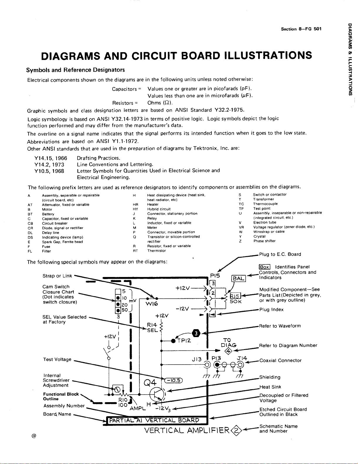
Section8-FG501
IT
DIAG
RAM
S
AND
CIRC
U
B
OA
R
D
I
LLU
STRATIO
N
S
Symbols
E
lectrical
Graphic
Logic
f
unction
T
Abb
Other
symbolsand
symbology
performed
h e
overlineonα
reviations
ANSI
Υ14.15,
Υ14.2,
Y10
.5,1968
T
hefollowing p
Α
Assembly,sepa
(circuitboa
Attenuator,
AT
M
Β
oto
BT
B
attery
C
Cap
B
C
C
R
DL
DS
Ε
F
FL
T
he
acitor,
Circuit
Diode,
Delaylin
Indicati
Spa
rkGap
Fuse
F
r
ilte
following
CamSwitc
ClosureC
(Dotin
switchclosure)
an
d
R
components
arebasedon
standards
1966
1973
refix
rd,
fixedorvariab
r
fixedor variable
breake
signalorr
e
ng d
evice
,Fe
special
h
dicates
eference
is
basedonANSIΥ32
and
signal
shown
class d
may
name
Designators
on
esignation
differ
ANSIΥ1
are u
that
Drafting
L
L
E
letters
rableorrepairab
etc)
r
ectifie
(lamp)
rr
ite
bead
symbols
h
art
P
ine
ConventionsandLettering
etter
Symbols
lectrical
are
le
le
r
t
hediagrams
Capacitors
from
indicates
sed
ractices
E
ngineering
use
d
appear
may
he
following
one
r
V
alues
V
alues
h
ms(Ω).
basedonANSIStandar
greater
o
lessthanone
Resistors
letters
areint
=
=O
are
.14-1973intermsofpositive logic
u re
n
al
r'sd
ata
performs
.
themanufact
sig
the
.
preparationofdiagramsbyTektronix,
i
nth
that
.1-1972
e
.
.
for
Quantities
Used
inElectrical
.
as
referencedesignatorstoi
Η
H
eatdissipati
h
eatradiato
HR
H
eate
ΗΥ H
J
Κ
L
Μ
Ρ
ο
R
FITThermisto
t
h
on
r
ybridcircuit
nnector,
Co
R
elay
I
ndu
ctor,fixedor variable
M
ete
r
Co
nnector,movableportio
T
ran
sistoror
r
ectifie
r
R
esistor,
fixedor
e d
iagrams
r
d
ng d
evice(h
r ,
etc)
stationary p
silicon-contr
variable
:
entify
~-12
units u
nless
notedotherwise
are
inpicofarads
areinmicrofarads(μ
dΥ32
.
L
ogic
its
i
ntendedfu
Science
eatsink,
ortio
n
olle
a
components
n
d
F15
V
-~
'Ι2
'
ΙΙ
nd
Ι
.2-1975
symbols
nctio
Inc
.
are
or
5
:
F
) .
(p
F
) .
.
depictthe
n
whenitgoes to
:
assemblies
Switchorcon
S
Τ Tran
TC
T
ΤΡ
Testpoint
U
Asse
(i
V
E
VR
V
Wir
W
Υ
C
Ζ Ph
D
AL,
-""
ΟΚ
logic
h
e
t
low
state
h
e d
on
sfo
h
erm
mb
n
r
teg
lectro
oltage
estraporcable
r
ystal
aseshifte
Plug
ΒοχIden
Co
~Indicatοr
M
od
PartsList(Depictedingr
o
r withgrey
-Plug
iagrams
t
tacto
rme
r
le
oco
up
ly,inseparableornon-repairable
atedcircuit,
ntube
regu
lator(zenerdiode,
r
E.C
to
ntrols,Conn
s
ifiedCompone
I
n
dex
.
r
etc
.)
.
B
oar
d
tifiesPanel
ectors and
n
u
tline)
o
.
etc
t-See
.)
ey,
Fun
ctionalBloc
O
u
tline
AssemblyNumber
k
F
210
ΙΟΟ
W
r to
aveform
R
efe
I~PL
A
VER
TICA
LAMPL
IFI
ER
Page 56

CKT
NO
C34
C40
C72t
C73t
C74t
C75t
C76t
C77
C78
C79
C80
C89
C95
C120
C150
C170
C190
C191 Η5
C235
C242
C250
C251
C271
C279
C281 Κ
C291
C294
C297
C400
C406
C410
C415
C455
C482t
C485 C5
C490 D6
C495
C
R
100 Η30445
C
R
101
C
R102 Η 4
C
R103 Η 4
C
R150 G1
C
R155 G1
CR
156
CR
158
CR
160
CR
162
C
R
170
C
R
175
R
C
176
R
C
178
R
C
180
C
R182
C
R215
C
R
218
G
R
ID
CKT
L
OC
No
L
2CR230Ι2
C
E3
Ι1CR242L4 R
C
12
C
Ι
3
Ι
CR
3
Ι
3CR 248 Κ
Ι
3CR285L6
Ι
3CR
Ι
3CR400 Β
F4
C
R450
C
R490
F
3
F
5 R54
G4
G1 J
81 F5
E
1
Η4
Q45
L
4
Q48
Μ
4
Q80
Ν2085
Ν4Q90
J6
Q120
Κ
5
Q125
5
Q130
L
6
Q138
L
5
Q150
Κ
6
Q170
D1
Q225
C2
Q230
D2
Q240
D2
Q242
D2
Q250
D5
Q255
Q270
0276
E4
Q280
Q285
Q290
Q295
Q298
Q400
Q410
Q415
Q420
Q424
Q430
Η4Q447
Q460 D5
Q468
Q472
Q474
G2
Q485
F30
488
F
3
G3
F2
R10
E2 R
11
E3 R13
F3 R
15
F3
R
18
F3 R
20
L2 R
30
L2
R32
GRID
L
OC
R240
R245Κ3
R246 Κ
L3 R
247Κ3
290L6 R
3 R
3
1
D6
CS
Η
3 R
G3
F
S
G4
G4
Η
5
Ι
5
Ι
5
Ι
6
G1
Ε
1
L
3
Ι
2
L3
L4 R
J
5 R
J
6
Κ 5
Κ 5 R87
L
5
Κ6
L
6
Μ
6
L
4
Β 2
Β
1
D2
Α
5
Β5
C3
Β
6
Β5
C4
Β4 R
Α
4 R
C5
C6
μ
2
ς
3
L
1
L
1
L
1
Κ2
L
1
Μ
2
CKT
No
R
34
37
38 Κ
R
39
41
R42
R44
R45
46
R
51
R
52 Η
R
53 Η2
R
55
R
56
R57
R
58
59
R
60
R
61
R
62
R
63
R64
R
6 6
R66 Κ
R
67
R
68
R
9
6
R
70-
R
72
R
73
80
81
R
82
*t
R
85
R
88
R
89
R
94
R
95
R
96
R
99
R
100
R
102
R
105
R120
R
121
R125
R
127
R
129
R
130
132
135
R
137
R139
R
141
R143
R145
R150
R
151
R
152
R
153
R
155
R156
R157
R
G
(S
GRID
CKT
L
0C
NO
Μ
2 R158
L
1
R
1
R
Κ
1
R
E3
R162
D3
R163
D3
R
D3
R
D3
R
Η2
R
2
R
R176
Η3
R
3
J
R180
J
3 R
J
3
R
J
3
R
J
3 R
J3R
Η
2 R
G2
R
198 Η
G2
R
199 Η
G2
R
J
J
Κ
J
J
F
FS R
GS
G4
F
F
G4
F4 R
E5
F
D5
Ε
F4
Ι
Η
Η5
Ι
15
Ι
Ι
Ι
Ι
Ι
5 R272
Ι
5
Η
Η
Η
Η
G1
G1 R284
G1
F
F2
E2 R
204
3
R
205
3
R
206
3
R
208
Κ3
R
210
Κ3
R
211
3
R212
1
R
215
2
R
216 C3
5
R218
220
R
222
R
225 Κ2
3
R
230
4
R
231
R233
234
R
237
4 R240
R242
5
R
251
R252
2 R254
5
R256
R
258
5
R263
R
265
5
R
267
5
R268 Κ
5
R
269
6
R
271
R273 Κ
5
R275 J
5
R277 Κ
6
R279 Κ 5
1
R
281
R282
R
285
2
R286 Κ
R290
291
ID
L
OCATIO
N
B020000-BELOW)
GRI
LOC
F
2 R
159
F
3
1
6 0
G2
161
F3
G3
F3 R
170
F
171
172
173
175
178
182
190
191
194
195
196
1
Ε
1
F
2
Ε
1
F
3 R
F
3 R412
F
3 R415
G3
G3
G
G5
F6 R
Η6
G6
5
5 R
F
6 R445 85
G6
F
6
E5
E5
D3
E5
L
3
L
2 R
L
3
L2
J
2 R482
Ι
2 R
L
4 R486
L
4 R487 D4
Μ
3
L
3 R495
L
3
4
Η
5
J
15
5
J
J
6
Μ
4 U30
Κ
5
J
5
5 U
J5
J6
J5 U
5
6 U
6
J
5
L
5 U
L
5
L
5
5
L
S
L
5
NCH
D
CKT
NO
294
R
296
R
296
R297 Κ
R299 J
400
R
403
R
405
R
406
R410
411
R417
R
420 Β4
5R422
R
424
430
R
431
R
434
R
441
442
R
446 Β5
R
450
R
452 C6
R455
R
461
R464 Β
R
465
R
468
471
R
473
R
475
R
481
485
R493
S50t J
S250
U
15
U40
U
45
48 E4
U
80
U
195
235
U
410
420 Β4
U
430
U
440 Β5
U
460 83
470 Β4
U
480
ART
GRID
L
OC
Μ
5
Μ
5
L
5
6
5
82
Α
2
C2 VR
C2
E2
C2
D2
D2
E2
Α
4
Β
4
C3
C3
C4
Α
5
Α
5
DS
D5
Β
3
3
Α
3
C4
Β4
Α4
84
D5
D5
C5
C5
Α
5
L
1
4
03
Μ
1
L3
E4
F
4
F
5
G5
L
3
C2
C3
C5
CKT GRID
NO
VR
VR
VR
VR
VR
V
VR
VR
VR
80
85
150
170
195
R205
21
225
237
405
8 L
L
OC
G4
G4
G2
E2
Η
6
E5
2
J
2
Μ
3
8
2
.
Page 57

.,
ιΜΡΟΝΕΝΤ
BelowSNB020000
L
OCATIO
N
G
R
ID
W"M
vy
~~tiί
.
:
.,
",
...
.,
.
ι
.
~;..,.. .ι,
.,,
;
...,
.
.,
Να
.
ι
Ι
νη
1431-
*
See
PartsList
tLocate
d
on b
fo
rser
ial
ackofboard
n
umber r
.
anges
.
"
,
.
.
,
._"..`ί
Ιι1^Ιι1
.
:
Μ
ι
:--~
α
ι
W
Ι
"Ι~
A
R
D,
WΙW
ι
"
,
.,ω,"ω ν
ω
ω
Page 58

α
νο
z$
Ο
a
ΟΖ
Jy
ΓΛ
F-
α J
IL
CO
MP
O
NEN
B
elow
Ν
SNΒ
T
02
m
?
Ο
m
ΝΟΤΕ
;
COMPO
NEN
CK
SID
E OF
TS
S
O
WN
WITH
DA7fiHEDLINES ARE
LOCATED
ON
BARD,
Page 59

FG
!
P
HAS
E
+17
ν
I
V
NPU
+CURREN
C
F
T
+17
S
+20
REF
UPPL
V
0
Y
S
(+
C
SOURC
UPPL
URREN
V
Y
T
E
)
-17
S
UPPL
(-CURREN
SOURC
V
Y
E
)
UR
T
CE
RENT
UEN
FRE
Q
UENCYVERNIER
FRE
Q
+20
S
DC
UPPL
V
PL
Y
SINI
SHAPI
-20V
Ητ
CY
S
UPPL
REF
Y
C
-20V
DC
PL
S
UPPL
Y
FUN
CI
S
ELE
C
Y
S2
S
+5
UPPL
V
Y
5
V
S
UPPL
Page 60

FG
501
BLOCK
DIAGRAM
GATE
INPUT
+20
V
AMPL
J
VVV-
OFFSET
-20
TRIG
OUTPUT
V
Page 61

C
K
T GRID
NO
L
C34
C40 E3
C72t
C73t J
C74t
C75t
C76t
C77*
C78
C79
C80
C85
C85'
C89
C95
C120
C130
C150
C162*
C170
C190
C191* Η
C196*
C204*
C211
C235
C242
C250
C251* Ν5
C255
C271
C279* Κ 5
C281
C286* Κ6
C291
C294
C297
C400
C406
C410
C415
C455
C482*tD5
C485
C490
C495
C
R
15*Μ1
C
R
16*Μ1
R
17*Μ1
C
C
R
45*
C
R100 Η4
CR
101
C
R
102
R103 Η4
C
C
R150 G1
C
R
155
C
R156
C
R158
ΓςR160
C
R162 E2
C
R170Ε1
C
R175
C
R176F3
C
K
T
OC
NO
Κ2
C
R178 F3
C
R180 F3
Ι
1
C
R182
R
2
C
215
R
Ι
3
C
Ι
3
Ι
3
Ι
3
Ι
3
Ι
3 C
F
F
G4
G4
E5
Η
Ι
4
G1
F
F
Η 4J81
G6
F6Q48
D3
L3Q85
Μ4Q90
Ν3
Μ
J
Κ5
L6
Μ5Q240
Κ
D1
C2 Q255
D2 Q270
D2
E4
C5 Q290
D6 Q295
E5
E4
Η4
Η4
G2 Q474
G3 Q485
F2
218L2
C
R230Ι2
C
R
235*
C
R240L3
C
R242L4
R245 Κ
4
C
R246 Κ 3
R247
3
C
C
R248 Κ 3
R
C
285L6
C
R290L6 R
5CR
400
C
R
410*
C
R
450
3 C
R
490
1
5
Q45
Q80
Q120
Q125
Q130
3
6
Q138
Q150 G2R65
Q170
Q225
Q230
6
Q242
Q250
Q276
Q280
Q285
Q298
Q400
Q410
Q415
Q420
Q424
Q430
Q445
Q447
Q450 D4
Q468 C4
Q472
Q488
F2
G3
^10
R
IDLOCATIO
G
N
B020000-UP)
(S
K
T
151
153
158
159
160
161
162
163
170
171
178
180
182
190
191
194
196
198
199
204
210
211
216
230
231
251
252
267
271
272*,λ
273*
R
214*
R
G
ID
L
OC
G1
G2
G2
F
F
F
E2
F
E2
E3
F
Ε
Ε
F2
E2 R410 E2
F2
F2
E2 R415
E2 R
Η5 R420
G5
G6
G6
Η
G6
F
G6
F
Ε5
E5
D3
E5
L
C3
L
L
L
Κ
J2
Ι
L
L
Μ
L
L
Ι
J
Ι
J
J
Μ
Κ5
J5 U
J5
J6
Κ
Κ
J
G
R
ID
C
K
T
G
R
ID
L
OC
R
R
R
E3
R
L2
R20
R
L
3
3
Κ 3
1
Β
C2
D6
C5
F
5
Η
3
G3
F5
G4
F4
Η5
Ι
5
Ι
5
Ι
6
F
2
L
3
Ι
2
L
3
L
4
J5
J
6
Κ 5
Κ5
L5
Κ
6
L
6
Μ
6 R
L
4
C2
Β
1
Β
2
Α
5
Β5
C3
Β6
Β5
4
Β
4
Α
C5
C6
Μ
2
NO
11
13
15
18
27
R30
R32
R34
R37
R38 Κ
R39 Κ
R
41 E3
R42
44
R45
R46
R
51
R52 Η2 R
R53
R54 Η
R
55
R56
R
57
R
58
R
59
R
60
R61
R
62
R
63
R64
R
66
R67
R
68 Κ
R69 Κ
R70
R72
R73
R80 E5
R
81
R82
R85
R87
88
R
89
R
94
R
96
R
99
R
100
R102
R105
R120
R
121Η5 R265
R125
R
127
R129
R130
R132
R135
R137Ι5
R
139
141Η5
R
R
143Η5
R
145Η5 U
C
L
OC
NO
C3
R150 Η
L1
R
L1
R152 G1 R
L1
R
Κ2
R155
F4
R156
L1
R
Μ
2 R
Μ
2 R
L1
R
1
R
1
R
R
D3
R
D3
R172
D3
R173
D3
R175
Η2 R176
Η
2
R
3
R
3
J
R
J
3
R
3
R
J
J 3 R
J
3 R
J
3 R
Η
2
R
G2
R205
G3
R206
G3
R208
J3
R
Κ
3
R
J3
R212
3
R215
3 R
Κ
3
R218
J
R220
1
J2
R222
R225
F5
R
F4 R
F
4
R233
G4
R234
F
4
R237
G4
R240
E5
R242
E5
R
F
4 R
E4
R254
F
4 R256
12
R258
Η
5 R263
Ι
5 R
Ι
5
R268 Κ
15
R269
Ι
5
R
Ι
5
R
16
R
Ι
5
R275
R277 Κ 6
R279 Κ5
NCHAR
C
K
T
G
NO
R
1
R282
R285
R286
R
2
R
2
3 R
3 R296
1
1
1
L
281
J
L5
2841-5 U
L5
L5
290
L5
291
L5
294
Μ
R295
Μ
L5
R297
L5
R299
J5
R
40082
R403
Α
R405
C2
R406
C2
R
411
D2
R
412
D2
D2
417
E2
84
R422
Α
R424
R430
R
431
R434
R
441Α6
R442
C3
C3
C4
Α
5
6
6 R445Β5
R446
R450 D5
R452
C6
R
455 D5
3
R
461
R464
Α
2 R465Α3
3 R468 C4
3 R
471
2
R473
Α
R475 Β4
2
R
481
4
R482
4
R485
3
R
486 C5
3
R487
3
R493
4
R495
5
5
6
S50tJ4
6
S250
U
15
30
40 E4
U
45
U
48
80
U
195
U
235L4
U
410
U
420 Β4
U
430
440
03
Μ
L3
F
E4
F
G5
C2
C3
Β5
4
5 U
6 U
6
5
6
Β
Β
83
Β4
D5
D5
D5
D4
Α
L
T
R
ID
C
K
T
G
R
80
85
195
205
225
237
405
ID
L
OC
4
C5
G4
G4
Η
5
E5
L2
J
2
Μ
3
C2
OC
NO
U
460 Β3
5
U
470 Β
480
VR
VR
5
VR
VR
5
V
R218
VR
VR
VR
2
4
4
5
5
3
4
5
1
1
4
5
Page 62

OCATIO
150
Mix
α
- "
c
:
.,
:
.
ι~:
ό
CR103I
r
',
C120
1
7-1
-
Γ
υ
.
φπ
,"'
Ο
ά
8120
ι
Q1
"
"ι\
Ι\,
\ι
\~
Οφ1
R
G
ID
N
εκτ
NO
C34
C40
C72t
C73t
C74t
C75t
ί
1
`ί
φ ~
Q225
Q24o
~
Ο1~Γ
°Γ°
Ο C
ι
OaC
I
CE
~Ί\ιι
C
R
215
α
,
CE
C72
~~1~
α
:
ι
230
ΤΡ
.
Ν
Ν
α
225(Υ
VR
~
~
-8
ΤΡ
-9
Ν
α
Λά
~
ΝυΝ
Ο
Λ
α
Ν
Ν
α
φ
!~~~
C73
R
S
~R10
Q23
,,
R230
C
.
ιι
'
α
Φ
Λ
υ
Ν k
ύ-Q242
.
AOMA
S50
;
ι
,
C
R
1 r
βή
ι
L115
η
ΓΙ
αΙ
`
υ
`
ΙΓ
0C
.
α
ο
Cr
,
υ
235
U
σ
V
Ν
υ
.
1~71"ι
Ι\
ι
~
~
ν ν
G138
1
Τ
~7
\\
Q
.
Ί
' ~Ι1
ΊΙ
\\%
λ-25
ηα
ω
Φ
Ν
Γ
0130
~
R 135
.
Ο
Μ
Ν
ά
Μ
Γ
\
Ί
Ό
Q
.
Ο
1
φ
Ο
1
Ν
α
Ι
νΙ,\
01
Ν
W
ί=ι
Τ
1
ICEN;
U
φ
t
Να
ίΙ
\
0276
\
10270
α
;
ΓΜ
Ι
φ
ν
Ι
Ν
α
Ν
Ι
α
ϋ
Ο
<
ο
QΟ
ΛΛΙ
-
.
Q2~5 0`90
Φ
Ν
ύ
Ι
028
υ~1
ΝΙ
~
Ιν"
ίί
a
r
Ί\
Ια
'Ι,
\Ι~`
MR
ι
Ο
1
ΝαΝ
'
~
:~.;J
:)11
0295
//
C7
β
t
C77
C78
C79
Ce0
C85
ε85ι
C89
C95
C120
C130
C150
ε16τ
C170
C190
191'
ε
C796'
C204'
ε
211
C235
C242
C250
C251'
C255
C271
C279'
C281
C28β'
ε
291
C294
C297
C400
C40
β
ε
410
C415
C455
C482'
C485
"
'
C490
1431-10
C495
"
SeePartsList
tLocate
'Alte
d
rnate
forse
b
ackofboard.
on
location
rialnumber
.
r
anges
CR15'
CR16'
R
17'
.
C
CR45'
CR101
R
C
10'
R
C
10
:
R
C
10
.'
CR151
CR151
CR151
CR151
CR161
CR1β~
CR171
CR171
CR171
Page 63

CO
MP
O
NEN
s
ηιsο
TLOC
οοοο
2
-uα
REVG,JUN
1978
Page 64

si
W
aveformconditions
FREQUEN
V
a
riable
CY
MULTIPLIER
PHASE
T
OFFS E
FUN
CTIO
N
A
MPL
:
Hzdial
10
Cal
10'
in (off)
i
n (off)
n
ewave
f
lly
clockwise
u
ΤΡ
ΤΡ5
40
0
6
ΤΡ
7
0
ι
m
Ζ
m
D
ι
U195-10
Ο
y
FT-T
:1-
11 1 1
Page 65

τ2ον
Q
CRl4D
c414l
G
R
GP-24
β
-
-
(Raw)
2
3Ο
24Z
R
4-7k
ι
-1
14
5245
(
εουαω/R
(
ΡΝΑ
+20
Rl+
.
ίουΙ
PULL
Vt
ι
λ
.
S
;
V
VCFΙΝΡυΤ
GAT
E
J2ι5
ΙΝΡυτ
y
RIi
a.s
ΑΤΕιW
k
+2
c
κσF)
'24
Ι
ον
τse
`,
UIS
υ
R
ΖΙβ
Z.4
άίι
~ιι~
\
(REF)
k
ν
(ό
LΓ
L)
R23
S
34.&W
.
ιον
+
VR
216
I~
V
V
}20
i)
(
R
222
F
Rl25
ΙΚ
2scR
iι6
β
s
ν
PHASE
-2Ο
(DGΓL)
24
.!
Κ
c R130
V
F
0.
EYViNC
FR
V
Ν
t®U"
ERNI
Rll
100
"0.
ν
NCV
R15
ιοΚ
+2014
(REF)
+2Ον
ίηε
C
ΑΜΥΝ
550
TAILS
5οffDE
κ1Ο
CAL
-2Ου
Γ/
ο
ssO
F>
U
30
ι
CONNECTION
ΑΤβ
G
CΣNTER
t3 λ1
642400O
I ι
.ae3
SER
DETAILS
RE.MO'
μη
TR14OUTPUT
Ff
G
501
JeO
U80B
(ι
BOA
RD
Ι
U80G
VR
198
(
.V
-
τον
(Raw)
FEB
RE
VD
W
1S
Page 66

G136
Ζ31
51,
,
Q455
+
τον
(R
a
F)
V0.1
S7
1
ον
R137
2.41ι
+2
Ον
(R
E
F
)
0
GL
i
Ι
η
c
0.τ
30
Q23
ρ
C142
R
2"2
4
.71L
6
3
Ζον
-
ίο
14t
ι
147
(PHASE)
Co4c.ω/α
+2Ονφc
H
OLD
SS0
DETAILS
5S0
4"ι)
-
τον
(RaF)
τ
35
βι1Ο
1
οο
G1.12
τ4θ
C0
.
C
R
G
R
C
R248
_ -ττ45Α
(
-CAM1914
102
SEE
Ρ/Ο
ΙΙΕΕΟlTAlLS
CR
C0
.103
24
β
140
λ
4
CZ
242
αΡι
)
ν
(
UPPER
I
L
LEVEL
~
ν το
515
CIL11r2
Ο
Λι
το
τ
τSΟ
νι
)
+τον
ί
DGPL)
R
ιτα
V RΦ50
9
Ο
Q125
ι
+
τον
(
Οειι
)
R
1i7
41
+τον
(αrι)
Q150
®
®
44
.2
't5
.1431
1.1Κ
®
too
GA7
CΣΡ1ΤΕR
'44
IRIg5
4V
)
FE
C
ΟΝΝΕ
ςΝ
ΘΒ
VRl
U
195A
U
IgS
-
τον
(star)
B 19
E
11
0.ι96
ΘΟ
Oi
V
SIC,
Τ
B
CΤ!
2
ίΝά
+
τον
(RIkT)
9
ΟΝ
ΟΟΟ
0.206
75ΟΟHe
REMOVE
0
D
+10
(Rεσ)
-2ον
ν
REF
ΙΙΚ
+4.SV
0LT5^+ΑΜΡ
s
w
χ
71M11J4"\
C
R
181
VE L
SEEPARTS
VALUES
RANGES
OR
44.7.
DEPICTED
G
75
LIST
AND
SERIAL.NUMBER
OFPARTS
IN
mWrLR..T
FOR
GREY
100
EARLIER
OUTLINED
.
0
R
Q
οειι
13
.7
Q170
αι7
τ
(
-
αιι
τον
ιοο
)
η,LOWER
LE
3.'D2κ
-1
ον
(ocr~)
L
to
C1ΑΟ
q
-3s
01W
.
1
κ
Page 67

τΟν
+
(DCPL)
ΓΖ1Hr COMP~
+ι7
~F20V
(
-
(DCP
οεΡι
)
R
τθ
82
,
λΟν
L)
Ρ/Ο
47,,.ι
+10
V
+
τον
(DC
PL
)
R
254
R
5
Q2s0
R
λSΙ
810
7
ΜΑΙ
B
OA.
ΑΊ
.1
Ν
2S4
ΙΟ
2.4Κ
Q255
F
A
MPL
ιR240A
I
k
V
Α
?,
UNCTIO
N
F
B
OARD
1418
FR
βΙΟ
R
F
R
FROM
Αιι
O
Ι4Ι
Τα
Q4!
ccw
M
5
O
M
~
"
9
0-.
c
Ι
ιΙ
Ι
ι
Ι
Ι Ι
ί
Ί
ΙΙ
ι ι
-ι7νΙ
Ι
Ι Ι
CC
λ 1
W
J
Z
JV
\
ΙΙΙ
ι
Ι
Ι
Ι3Ι5Ι
4
Ι
Ι
Ι
Ι
ι
Ι
ι
Ί
Ι
Ι 1
Ι
Ι
ι ι
Ι
Ι
Ι
4
7 θ
ι
~
Ι
i
Ι
Ι
9Ιιο
Ι
Ι
ι
Ί
Ι Ι
Ι
υυ
Ι
1
ι
ιι
7
C
W
F
1
501
G
FUNCTION]
5250
U
REV
L
Μη
J
Ο
R
ROB
45k-
R
αs
4.SΜ
Cw
Ι
Ι
Ι
Ι
Ι ς
Ι
Ι
Ι
Ι i
Ι
Ι
Ι
Ι
Ι Ι
Ι
Ι
Ι
Ι
Ι
Rι.2
Ι"smΙ ι
-
πν
OUTPUT
το
448
Α
43
.
4T
οιι
βΟ
9
Ι
1
Ι
f
Ι Ι
Ι
Ι
Ι
Ι
Ι
Ι
1431-Ι6
Ι
Ι
το
υη4θ
Ι
Ι
Ι
Ι
Am
Page 68

Ι
ιΙ
Ι
ουτΡυτ
π
.54
oPG
NBGTwG
(
HOLD
D
ΕΤεΝτ
ι
9
ν
07 Γi'
Γ
ΤΟyAT
Q110
"
ιι
is
ΙΙ
Ι
ιι
Ιι
F
17
-
-ζ04X4O
SEE
VALUES
RANGES
OR
ιβ
Ι
Ι
Ι
Ι
PARTS
DEPICTED
C79
9-35
Ιο°χΙ
TIMING
AND
OF
LIST
SERIAL
PARTS
TIMINy
FOR
IN
GREY
ι
ΜυιτΙΡιιCβ
ss
V
-I7
~
ο
ΡΟΕΙΤΙΟΝΟ
EARLIER
NUMBER
OUTLINED
.
EN
~
OUTPUT
149Ι- 16
AMPLIFIERANDSWITCH
D
E
TAILS
D6
H
Page 69

RεFεκe
C
νβλεΝΤ
υεε
VAC
25
C4oo
75
ομ
F40,
Q400
R
405
+20V
0
.495
2
ΙΚ
C40(
το
4.7ηι
VOLTS-"
.
F
8411
1
.49
Κ
/
VR4o5
(..IV
+
ΟΟ
V
+S
Q410
R
417
3
U
4
λΟ
CO
+ιΙ.5
+
MMON
25VAC
ιΙ.5ν
G1ND
V
4-2
R493
4
"+ΙΙ
.7
C
R490
VO
L
.5
TS
Q450
R
441
κ
V
470
G490
76οη
40
R4
81
4.0 Κ
R
487
3
Q488
F
V
F
Γ
,
501
REVG,JUL
1978
Page 70

ιλΑ
(LOGATfiD1Ν
`
ΜΑΙΝF0.ΑΜ8
7
Α
R
424
1
.5
~
~
υιιs-
76
Ρ
/ΟAl
MAIN
BoAsto
POWER
ιτ
1431-
75
47i
.
17
SUPPLY
SEE
PARTS
LIST
FOR
VALUES
RA
OR
D
εΝ
τ
73
NGES
DEPICTED
AND
OFPARTS
SERIAL
IN
GREY.
EARLIER
NUMBER
OUTLINED
Page 71

ME
P
ARTSORDERINGINF
Rep
lacemen
tparts
are available
Tektronix,
accommodateimp
andto
d
evelo
impo
informatio
number,ser
i
mpr
repr
number.
m
anual.
Inc
.FieldOfficeor
ChangestoTektronixin
rovedcom
give
youth
eben
pedin o
rtant,when
If
α part
oved p
ese
ntative
Changeinformation,ifany,islocatedattherear ofth
S
ΧΟΟΟ
ΟΟΧ
urengin
order
n in
your
ord
ialnumber,andmod
youhaveordere
art,yourlocalTek
will
con
PECIALNOTES
P
a
rt fi rstadded atth
P
artremoved
representative
strumentsare
ponentsastheybecome
efitofthelatestcircuitimp
eeringdepartment.Itisth
i
ngparts,
er:Pa
d h
tact
you concerning
ORM
ATIO
fromor
through
.
sometimes
toin
cludethefollowing
r t
number,inst
ificationnumbe
asbeenreplacedwit
tronix,
AND SY
is
afte
r thisser
rument
Inc
.FieldOfficeor
any
MBOL
r
ialnum
se
ial
numb
REPL
HAN
C
N
yourlocal
available,
rovemen
r ifapp
h αnewor
ch a
ngeinpart
S
ber
er
made to
erefore
typeor
licable
AC
ts
.
is
EABLE
ICA
L
PAR
T
hismec
r
elatio
nship
s
usedin t
.Followingis
he
d
esc
1
2 3 4 5
Assembly
Attachingparts for
DetailPartο/
Attaching
Parts
Attaching
AttachingParts
the
item
itmoun
I
nde
nteditems
i
nden
tation.Theseparatio
attaching
Attachingpartsmustbe purch
s
p
parts
ecified.
TS
I
NDEN
TATIO
han
icalparts
rip
tio
n
col
and/orComponen
Assemblyand/or
Assembly a
p
a
rtsfor
o
f
DetailPart
p
arts
always appea
ts,wh
ilethedetailpartsareindentedtot
arepart
.
of,
N SYST
listisi
nde
an exampleoftheinden
umn
.
N
t
nd
/orComponen
DetailPart
for
Par
ts
ο/DetailPar
rinthesamei
and
incl
uded
n symbol
ase
---'
d sep a
Section
9-FG
EM
nted toind
ame &
Com
with,th
---ind
rately,unlessother
icate
tationsyste
Description
pon
ent
t
t
nden
enext
icatesthe e
tatio
heright
hig
n
nd
wise
ite
9ο
1
m
m
as
.
h
er
of
F
IG
UREAN
Items inthissectionarereferen
numb
ers
to theillustrations
I
PTR
G
S
Z
NN
V
NCH
NUMBER
SIZE
ATO
LIG
NMEN
LUMINUM
EMBLED
EMBL
ENU
MER
ICA
OARD
ACKET
ASS
ERAM
IC
RCU
IT
OSITIO
VER
UPLING
HODE RAYT
RA
WER
G
T
ATOR
N
R
T
Y
WIRE
R
N
ADAPTER
A
EM
ASS
ASS
ATT
A
B
BR
BR
BRONZE
G
BUSHIN
C
CONNECTOR
CO
G
CO
DEGREE
D
ρ
ACTR ACTU
AD
A
LIGN A
AL
ASS
ASSY
ΑΤΤΕΝ
A
W
B
D
BRKT
BR
BR
B
SH
CAB CABINE
CAP CAPACITO
ER
C
C
HAS CHASSIS
C
KT CI
CO MP COMP
CO
CO
C
PL
CRT CAT
D
E
G
D
WR
UBE
GAG
D
IN
DEX
NUMBER
cedbyfigure
.
ELCTRN
ELE
C
ELCTLTELECTROL
ELEM ELEMEN
EPL
E
P
T
Q
ΕΧΤ
FIL
FLE
E
X
FLH
FLTR F
FR FRAMEorFRONT
F
STNR F
F
T F
FXD
GS
KT GASKET
HD
L
HEX HE
HEXND HE
HEX
SOC
HLC
PS
HLE
XT
NV HIGH V OLTAG
IC
ID
IDENT
I
MPLR
S
andindex
A
BBREV
ELECTR
ON
ELECTR
ICA
L
YTIC
T
ELECTR
ICALPAR
E
QUI
PMEN
EXTERNA
F
FLEXIBLE
FL
FIXE
HA
HE
HEL
HEL
INTEGRATEDCIRCU
INSIDEDIAMET
IDENTIF
I
MPELLER
T
L
ILLIST
ER HE
AT HE
AD
ILT
ER
ASTENER
OOT
D
NDLE
XAGO
N
XAGONALHEAD
XAGONAL
ICALCO
MPRE
ICALEXTENSION
ICATIO
AD
SOC
E
ER
N
TSLIST
KET
SSIO
IT
InthePartsList,anItemName
d
escriptionb
N
amemay
Nameid
entification,th
beu
can
tilize
IATIONS
IN
I
NCANDINCANDESC
I
NSUL
I
NT
LPHL
M
AC
ME
M
TG
NIP
NON
O
BD ORDER
OD
O
VH
ΡΗ BRZ PHOSPHORBRONZ
PL PLAINor
PL
ΡΝ
ΡΝΗ
PWR
RCP
RE
N
R
GD
RLF RELIEF
RT
SCH
SCO
SC
INCH
I
NSUL
L
I
NTERNA
DRLA
H MACHINE
CH ME C
M
N
WIRE
NOT
OU
OV
STC
PL
P
PAN HEAD
POWER
T
RECEP
RE
S
RIGID
RE
NR
SOC
PE
OSCILL
R SC
y α
sometimes
dwher
ATO
MPHOLDER
HAN
OUNTI
NG
I
PPLE
WIREWOUN
BY
TSIDEDIA
A
LHE
ASTIC
ART
NUMBER
TAC
SISTOR
TAI
NER
KET HE AD
OSCO
REW
ITEM
colon
( :)
.Because ofspacelim
appearasincomplete
e
U.S.
F
epossible
EN
T
R
L
ICA
L
D
DESCR
IPTIO
N SO
ER
E S
E Τ
AD
PLAT
MET
LE
PE
NAME
ederal
CatalogingHa
.
SE
SE
S
EM
SHLD S
SHLDR SHOULD
S
KT
SL
S
LFLK
S
LV
S
PR
SST
STL
W
T
ERM
THD THREAD
ΤΗΚ
TNSN
TP
T
RH
V
VAR
W
/
WS
X
FMR
XST
isseparate
CT SE
N
D SEMICO
ICO
G S
G S
G
HR
R
dfromth
itations,anItem
.ForfurtherIte
ndbookΗ6-1
SINGLEEND
CTIO
N
NDU
I
EL
D
UARE
NLESS ST
ITC
H
AL
SIO
N
TAG
H
SISTO
ERE
E
AD
RMER
CTO
D
G
EEL
R
H
SOCKET
SLIDE
ELF-LOCKIN
LEEVING
S
PRING
SQ
STAI
STEEL
S
W
TUBE
T
ERMIN
THICK
T
EN
TAPPING
TRUSSHE
VOL
V
ARIABLE
W
IT
W
ASHER
T
RANSFO
T
RAN
e
m
R
R
E
V
.
I
JULY 1978
Page 72

R
eplacea
Mfr.Code
00779
01295
05091
08261
10539
12360
24931
45722
55210
73743
74445
74868
77250
78189
78584
79136 WALDES,
79807
80009
83385
91836
93907
98978
ble
M
echanical
M
anufacturer
AMP,INC
TEXAS INSTRUMENTS,
G
ROUP
R
Τ
SPECTRA-STRIP
JACKSON
ALBANY PRODUCTS CO
D
YNAMICS
SPECIALTY
U
SM CORP
GETTIG
FISCHER
ΗΟLΟ-ΚR
UNKER-RAMO CORP.,THE
B
Ρ
HEOLL
O
F
ILLINOIS
SHAKEPROOF
STEWART
WROUGHT
TEKTRONIX,
CENTRAL
KINGSELECTRONICS
CAMCAR
INTERNATIONAL
.
Ι-
ORDINATE
BROS.,LONDON,
CORPORATION
CONNECTOR
P
.,
.
ENG
S
PECIALMFG.CO
ΟΜΕCO.
MANUFACTURING CO.,DIVISION
ALLIED
PRODUCTS CORP
TOOL
DIVISION
TAMPING
S
OHINOOR,
K
WASHERMFG.CO
INC
SCREWCO.
SCREWANDMFG.CO
Parts-FG
C
CORPORATION
CORP
ARKER-ΚΑL
ANDMFG.COMPANY
WORKS,
.
E
LECTRONIC
501
ROSS
INDEX-
INC.,SEMICONDUCTOR
.
LTD
DIV.OF
.,
CO.,INC
ΟΝFASTENER
.
AMPHENOL
.
INC
.
CORP
.
INC
.
.
CO.,INC
.
.
ΡΝΕUΜΟ
.
.
RESEARCH
MFR.
CODE NUMBER
DIV
.
RF
DIV
.
CORP
Address
ΡΟBOX
ΡΟBox
EXPRESSWAY
343
SNYDER
LAMPSON
7100
145WOODWARD
3560
MADISON
PO
BOX
446MORGANST
.
85,
B
ROOKST.WEST
31
33Ε.FRANKLINST
5700W.
5Τ.
CHARLES
630
CENTRAL
47-16
AUSTEL
2100S.ΟBAYST
ΡΟBOX 500
2530
CRESCENT
40
MARBLιEDALE
600
18TH
135
W
.
MAGNOLIA
TOMANUFACTURER
3608
13500ΝCENTRAL
5012,
AVENUE
AVE
.
AVENUE
AVE
.
OFF
ROUTE
.
.
PLACE
.
DR
ROAD
AVE.
.
BLVD
D
R
ROOSEVELT
ROAD
PARK
AVE
State,
City,
HARRI
SBUR
D
ALLAS,
BERKELEY
GARDEN
CROYDEN,
SOUTHΝORWALK,
CAMPBEL
45
HARTFORD,
.
.
GROVE,
I
NDIANAPOLIS,
SPRING
CINCINNATI,
D
CHICAGO,
ELGIN,
Υ
L
MILWAUKEE,
B
B
Τ
ROCKFORD,
BURBANK,
MILLS,
ANBURY,
ONKERS,
ANGISLANDCITY,
EAVERTON,
ROADVIEW,
UC
ΚΑΗΟΕ
Zip
PA
17105
G,
75222
TX
HEIGHTS,
CA
OH
06810
60650
60120
10704
WI
OR
IL
NY
IL
91502
CT
IN
PA
45206
06110
53207
97077
60153
10707
61101
92642
46227
KY
16875
SURREY, ENGLAND
SVILLE,
CT
CT
IL
IL
NY
,
CA
NJ
06586
42718
NY
07922
11101
9-2
4
R
E
V
.
κ
JULYι97
α
Page 73

Co
F
ig.&
IndexTektronixSerial/Mo delNo
P
No
1-1
-2
-3
-4
-5
-6
-7
-8
-9
-10
-11
-12
-13
-14
-15
-16
-17
-18
-19
-20
-21
-22
-23
-24
-25
-26
.
artNo.
337-1399-00
366-1422-00
366-1422-01
214-1840-00
366-1031-03
366-1031-08
213-0153-00
366-1170-01
366-1170-03
213-0153-00
366-1023-01
366-1023-01
366-1023-07
366-1023-03
366-1023-08
213-0153-00
366-1319-00
213-0725-00
366-1077-00
366-1077-01
213-0153-00
366-1004-00
366-1007-01
366-1007-05
200-0844-01
213-0153-00
354-0437-01
354-0557-02
211-0030-00
211-0088-00
131-0679-00
131-0679-02
131-0274-00
220-0497-00
210-1039-00
131-0955-00
131-0282-00
----- -----
210-0583-00
210-0940-00
-----
210-0583-00
210-0940-00
358-0378-00
333-1644-00
333-1644-01
333-1644-02
214-1513-00
214-1513-01
213-0254-00
200-0935-00
378-0602-00
352-0157-00
-----
E
ff
Β
010100Β019999
Β
020000
ΧΒ
020000
Β
010100Β139209
Β
139210
Β
010100
Β
139210
Β
010100Β059999
Β
060000Β139209
Β
139210
Β
060000Β139209
Β
139210
Β
010100Β139209
Β
139210
Β
010100
Β
090000
Β
139210
139210
Β
Β
010100Β139209
139210
Β
Β
010100Β099999
Β
010000
Β
010100Β103149
Β
103150Β125502
Β
125503
Β
103150
Β
103150
9010100Β109999
Β
110000
Β
139210
Β
010100
020000
Β
Dsco
Β
139209
089999
Β
Β
139209
139209
Β
019999
Β
.
1
nt
234
Qty
2
S
HLD,ELECT
1
KNOB
1KNOB
1.ΡΙΝ,ΚΝΟΒSECRG:0
1KNOB:RED--CA
1KNOB
1
.SET
1 KNOB:GRAY,4SIDED
1 KNOB:GR
2
.SET
OB:GR
2 K
N
NOB
1 K
1 KNOB:GRAY,0
OB:GRAY--
1 K
N
1KNOB
1
.SET
1 KNOB:GR
1
.SET
K
NOB
1
1 KNOB:GRAY,0
1
.SET
1KNOB
1KNOB
1 KNOB:GR
1
CAP,INSERT
2
.SET
1
RING,KNO
1
RING,KNOB
SCREW,ΜACHI
2
SCREW
1
CONNECTOR,RCPT,:BNCW/HARDWAR
1
1
CONNECTOR,RCPT,:BNCW/HAR
CONNECTOR,RCPT,
1
1NUT,
1 WAS
2
CONNECTOR,RCPT,:BN
1
CONNECTOR,RC
1RES
ΝUΤ,ΡLΑΙΝ,ΗΕΧ.:0
1
W
AS
1
1RESISTO
1ΝUΤ,ΡLΑΙΝ,ΗΕΧ.:0
1
WASHER,FLAT:0.25
BUSHIN
1
P
ANEL,F
1
1 P
ANEL,F
1 PANEL,FRONT
1LC
H,PL-INRTNG:P
1LC
H,PLUG-INRET
1SCR,TPG,THDCTG
1BASE,LAM
1
LEN
1
LAMPHO
5
RI
CAL:S
IDE
:
:LAT
CH
:GY,CAL/W/A
:5
SCREW
A
Y,0
.25
SCREW
:5
AY
:GR
AY
.127ID,0
PULL
:GRAY--PULL
SCREW:5-40
AY
SCREW
:3
:GR
AY
.127ID,0.5OD,0.531
SCREW:5-40
:GR
AY
:GR
AY
AY
,K
SCREW:5-40
BSKIRT
KIRT
S
N
,MACHINE:2
PL
AIN,HEX.:0.5
HER,LOCK:INT,0.521
STOR,VAR:(S
I
HER,FLAT:0
R,VAR
G,SLEEVE:
RONT:
RONT:
:
PHOLDER:0.29ODΧ0
S,LIGHT:GR
LDER:WHITEPLASTIC
.094OD Χ0.120INCH
L
RROW,0.127ID,0
-40
Χ 0
ID
Χ 0
-40
Χ 0
Χ 0
-48
Χ 0
Χ 0
NOB
:
0
Χ
:
:CLEAR,1ΤΟ
-56
E
:2
-56
:BN
C
(ATTAC
-28Χ0
C,
PT,
:FEEDTHRU
ΕΕR206AAND
(ATTACHIN
.25-32
.25IDΧ 0
:(SEER235AND
(ATTACHIN
.25-32
ID
PRE
SSMOUN
LASTIC
:
(ATTACHIN
:2
-32Χ0
EEN
R
eplaceable
N
ame&Descriptio n
.125 INCH,HEXSOCSTL
.706OD
.125 INCH,HEXSOCSTL
.392
.125 ΙΝCΗ,ΗΕΧ
.095 INCH,HEXSOCSTL
.125 INCH,HEXSOCSTL
.125 INCH,HEXSOCSTL
Χ 0
.25"82DEG,
Χ 0
.281"82DEG,
GPARTS)
HIN
ID
F
EMALE,W/HARDWARE
GPARTS)
Χ 0
.375 IN
G
Χ 0
Χ 0
.375 INCHOD,STL
GPARTS)
.392OD
,0.6
H
.466
OD,0
SOCSTL
H
10
FLHSTL
FLH
E
WAR
D
E
.562INCHHE
0
.625 IN
Χ
R206ΒEPL)
.19
245
H,B
C
D,STL
CH
O
EPL)
CAS
E
.312 IN
R
P
ARTS)
.312 INCH,B
T
.250,100DEG,
X,BRS
CHOD
RS
RS
FLH
LONG
ST
Mechan
L
icalParts-FG
fr
M
de
M
frPartNumber
80009
80009
80009
80009
80009
80009
74445OBD
80009
80009
74445OBD
80009
80009
80009
80009
80009
74445OBD
80009
74445OBD
80009
80009
74445OBD
80009
80009
80009
80009
74445OBD
80009
80009
83385OBD
77250OBD
24931
24931
91836KC79-67
73743OBD
24931OBD
05091
74868 74300
73743
79807OBD
73743
79807OBD
80009
80009
80009
80009
80009
80009
45722OBD
80009
80009
80009
337-1399-00
366-1422-00
366-1422-01
214-1840-00
366-1031-03
366-1031-08
366-1170-01
366-1170-03
366-1023-01
366-1023-01
366-1023-07
366-1023-03
366-1023-08
366-1319-00
366-1077-00
366-1077-01
366-1004-00
366-1007-01
366-1007-05
200-0844-01
354-0347-01
354-0557-02
28JR168
28JR270
31-279
2Χ
20224-402
20224-402
2Χ
358-0378-00
333-1644-00
333-1644-01
333-1644-02
214-1513-00
214-1513-01
200-0935-00
378-0602-00
352-0157-00
501
-1
-1
ΜΒ
R
EV.ΕJULY1978
9-
3
Page 74

Code
R
eplaceableMechanicalParts-FG
F
ig.&
IndexTektronixSerial/ModelNo.
No
.
P
1-27
-28
-29
-30
-31
-32
-33
-34
-35
-36
-37
-38
-39
-40
-41
-42
-43
-44
-45
-46
-47
-48
-49
-50
-ς1
-52
-53
-54
-55
-56
-57
-58
-59
-60
-61
-62
artNo.
401-0206-00
213-0088-00
213-0044-00
213-0138-00
210-0201-00
358-0481-00
386-2372-00
386-2372-01
213-0229-00
337-1713-00
337-1713-01
376-0051-00
376-0051-01
376-0049-00
354-0251-00
213-0022-00
213-0178-00
384-0209-00
384-0406-00
----131-0604-00
105-0378-00
200-1435-00
354-0219-00
401-0155-00
214-1704-00
214-1704-01
214-1704-02
214-1127-00
105-0377-00
401-0156210-0406-00
131-1248-00
211-0116-00
211-0008-00
211-0168-00
129-0080-00
----- ----131-0566-00
131-0604-00
131-1003-00
337-1418-01
211-0001-00
210-1008-00
342-0167-00
210-0583-00
210-0046-00
407-0579-00
211-0008-00
210-0921-00
E
ff
Β
Β
Η
010000
Β
Β
Β
Η
Β
8090000
Β
Β
-----
1
1 1
1 1
00
ΧΒ
Dscont
010100
8010203
010204Β099999
010100Β109999
110000
010100Β109999
110000
010100Η089999
010100Β089999
090000
020229
501
Qty
1 2
3 4 5
1GR
ASSY,SPRDCN:
2
SCR,TPG,THDCTG:4-24
2SCR,TPG,THD
2SCR,TPG,THD
1TER
MINAL,LUG:SE#4
1BUS
HIN
1
SUBPANEL,FRONT
1
SUBPANEL,F
4
SCR,TPG,THD
HIELD,ELEC:S
1
S
1SHIELD,ELE
1CP
LG,SHAFT,FLEX:FO
C
P
LG,SHAFT,
1
C
PL
1
2.RIN
4
4
1EXTENSIO
1
1
11.CONTACT,
1
1
1
1
1
1
1
1
4
1
4.SC
2
2
2POST,
1CKT
1.LINK,TERM.CONNE:0
19.CONTAC
1.CONNECTORBODY,:CKTBD ΜΤ
1
3.SCREW,MAC
3.WAS
1.INSU
1
1.NUT,PL
1
1
3.SCREW,MACHINE:4
3
G,SHAFT,
.
G,CO
.SET
SCREW:4-40
.SET
SCREW:4
EXTENSION
CK
T
BOARD
.ACTRA
. .
COVER,C
. .
RIN
. .BEARIN
. .SPRING,FLAT:CA
S
PRING,FLAT
. .
PRING,
. .'S
. .ROL
. .ACT
. .BEARING,CA
. .NUT,PLAIN,HEX.:4-40
. .CONTACT,ELEC:GROU
R,A
SCREW,MACHINE:4-40
SCREW,MACHINE
ELEC-MECH
BOARDASSY:MAIN(SEEΑ1
.SHIELD,ELEC:CAMSWITCH
HER,FLAT:0
SISTOR,VAR:(SEE
.RE
WASHER
.
B
RKT,RES.MTG:
.
.WAS
HER,MICA:0.50Χ0
FOR:5-32
FOR:4-40
G,S
LEEVE:S
RONT:
FOR:6-20
:SUBPANEL,F
C
FLEX:
UPLING:0
-40
NSHAFT:0.125OD Χ 6
SHAFT:0
ASSY:SE
ELEC:CKTBD
SSY,CA
AMSW
G,R
ETAINING:FOR0.25INCHSHAFT
G,CAMSW:FRONT
FLAT
LER,DETENT:0.125DIA
UATOR,CAMSW
M WSHR:4-40
SSE
T,ELEC:C
HINE
LATOR,PLATE:2.45INC
AIN
,HEX.:0
,LOCK:IN
N
ame&Descriptio
(ATTACHINGPART
Χ 0
Χ 0
Χ 0
PLIT,0.128
:
(ATTACHIN
Χ0
UBP
ANEL,F
RON
RON
R 0
.125 INCHDIA SHAFTS
FOR 0
FLEX:P
M S
MSW
(ATTA
(ATTACHIN
:4-40
:0.875INCHLONG
.125 INCHDIA
LASTIC
.251ID Χ 0
Χ 0
.188INCH,HEXSOCSTL
Χ 0
.125 INCH,HEX,SOCSTL
.125OD Χ 5
CON
DAR
SW,S
:(S250)
:
MSWDETENT
:CAMSWDETENT,0.008 INCH
:CAMSW
:
:REA
R
ND
HIN
C
Χ 0
Χ 0
Χ 0
.25INC
.086DIAΧ2
KT BD
SW,S
(ATTAC
HINGPART
:2-56
Χ 0
.09IDΧ 0
ι
R27
(ATTACHINGPART
.25
-32
TL ,0
.26IDΧ 0
-40Χ0
.141
S)
.25ΙΝCΗ,ΡΝΗSTL
.188INC
.188INC
GPARTS)
.375"100
T
T
Y(SEEΑ2EPL)
DETENT,0
Χ 0
GPARTSFORACTRASSY)
GPARTS F
.25INC
.25INC
EPL)
Χ 0
.25
H,PNHSTL
H,PNHSTL
ID
Χ
0
DE
.375INC
.064INCHLONG
.937INCH LONG
PR
,0.006 INCH
.010INCHTHICK
Χ 0
.125 INCHL
.188 INCH,B
.312 INCH,P
ORCKT BD
H,PNHSTL
H,P
NHSTL
EPL)
.375 INCH L
PR
PR
O
,3
S)
H,PNHSTL
.188"OD,BRS
H LON
G
S)
.312INC
.40"OD,STL
INCH,P
Χ0
.005 INCH
n
.25INC
G,
FLHSTL
SHAFTS
HOD,AL
NH B
NG
H,B
NHSTL
M
fr
M
frPartNumber
10539
83385OBD
83385OBD
83385OBD
78189
HOD
ΤΗΚ
ΤΗΚ
RS
RS
RS
ΤΗΚ
80009
80009
80009
93907OBD
80009
80009
80009
80009
80009
80009
74445OBD
74445OBD
80009
80009
80009
80009
80009
79136
80009
80009
80009
80009
80009
80009
80009
737432Χ
80009
83385OBD
ASSY)
83385OBD
12360OBD
80009
55210L-2007-1
80009
80009
80009
83385
12360
80009
737432Χ
78189
80009
83385OBD
80009
4511/DA
2104-04-00-2520
358-0481-00
386-2372-00
386-2372-01
337-1713-00
337-1713-01
376-0051-00
376-0051-01
376-0049-00
354-0251-00
384-0209-00
384-0406-00
131-0604-00
105-0378-00
200-1435-00
5103
401-0155-00
214-1704-00
214-1704-01
214-1704-02
214-1127-00
105-0377-00
401-0156-00
131-1248-00
129-0080-00
131-0604-00
131-1003-00
337-1418-01
OBD
OBD
342-0167-00
1214-05-00-0541C
407-0579-00
210-0921-00
F
25-MD-R
-
12161-402
20224-402
Ν
lReplace
9-
4
only
withpart
bea
rin
g thesameco
or
code
asth
l
e originalpartinyour
instrument
.
REV.
C
JULY1978
Page 75

Rep
F
ig.&
IndexTektronixSerial/ModelNo
No
.
P
1-63
-64
-65
-66
-67
-68
-69
-70
-71
-72
-73
-74
-75
-76
-77
-78
-79
-80
-81
-82
-83
-84
-85
-86
artNo.
210-0406-00
105-0376-00
200-1434-00
354-0219-00
401-0155-00
214-1704-00
214-1704-01
214-1704-02
214-1127-00
105-0375-00
401-0156-00
210-0406-00
131-1248-00
211-0116-00
210-0269-00
214-0269-00
214-0693-00
214-0579-00
214-2733-00
211-0004-00
342-0202-00
136-0252-00
213-0146-00
210-1270-00
386-3657-00
426-0724-00
426-0725-00
175-0825-00
175-0828-00
175-0829-00
210-0774-00
210-0775-00
----- -----
214-1061-00
E
ff
ΧΒ139210
Β
010100Β129999
ΧΒΟ
10204
ΧΒ
139210
ΧΒ
139210
ΧΒ
139219
ΧΒ
128340
ΧΒ
128340
ΧΒ
050297
Dscon
.
tQty12 345
3
.NUT,PLAIN,H
1
.ACTRA
1
. .
1
. .
1
. .
1
. .
1
. .SPRING,
1
. .SPR
1
. .ROLLER,DETENT
1
. .ACTUATOR,CAMSW
1
. .
4
. .NUT,PLAIN,HΕX.:4-40
1
. .
4.SCR,ASSEMWSHR:4-40
1.TERMINAL,LU
Χ
2.HEAT
3.HEATSINK,ELEC:0
9.TERM.,TESTΡΤ:0
1
HEATSINK
2
SCREW,MACHINE
2INSULATOR,PLATE:TRANS I
209
.
4SCR,TPG,THD
2WASHER,FLAT:0.141
2SUPPORT,PLUG-IN
1'
FRSECT,
1
FRSECT,
FTWIRE,ELECTRICAL:2WI
FT
WI
W
FT
1EY
1EYE
1RESISTOR,V
1 SPRING,GROUND:FL
SSY,CA
COVER,CA
R
IN
G,R
B
EARING,CA
S
PR
ING,FLAT:CAMSW
ING,FLAT
BEARIN
CONTACT,ELEC:G
S
INK
SOCΚET,PIN ΤΕ
PLUG-ΙΝ:ΒΟΤΤΟΜ
PLUG-ΙΝ:ΤΟΡ
R
E,ELECTRICAL
IRE,ELECTRICAL:6WIRERIBB0N,0.334
ELET
,METALLIC:0
LET,METALLIC:0
N
ame&Description
x.:4
-40
Ε
MS:(S50)
MSW
ETAINING:FOR 0
MSW:FRON
FLAT
G,CA
MSW
(ATTAC
G
:NONLOC
,XSTR:0
,XSTR:(2)
(ATTAC
:3-48
(ATTACHIN
FOR:6-20Χ0
AR:(SEER25 EPL)
Χ 0
:
:CAMSW
:CA
MSW
:0.125
:
R
:REA
R
OUN
D
HIN
Χ0.312INC
KIN
.312 DIAΧ 0
.25IDΧ0.75INCHLO
.40INCHLON
TO
HIN
Χ 0
RΜ:0.145INC
IDΧ.04THK,AL,
:
RERIBBON,0.531
:5WIRERIBBON
.152ODΧ0
.126OD
AT
laceable
.188IΝCH,Β
.25INCH
T
DETENT,0.006INCH
DETENT,0.008
T,0.010INCH
DET
EN
DIA
Χ 0
Χ 0
.188
GPARTSFORACTR
G,0
.257"MT
-202,A
ST
G
L
G
PART
S)
.125,PNH,STL,CDPLΡΟΖ
OR
H LONG
GPARTSFO
.313INC
.245 INCHL,
Χ0.23INC
SHA
.125INCH L
INCH,B
H,PNHBRS
.75
L
R CΚΤBD
H,P
NHSTL
.21
,0.334
HL,BRS
RS
FT
INCHΤΗΚ
RS
GHO
9 OD
FT LO
FTLON
FT LO
ΤΗΚ
THICK
ASSY)
LE
N
G
ASSY)
G
N
G
N
G
RS
B
Mechanical
M
fr
Cod
eM
737432Χ
80009
80009
79136
80009
80009
80009
80009
80009
80009
80009
737432Χ
80009
83385OBD
78584OBD
98978
98978
80009
80009
01295
00779
83385
80009
80009
80009
80009
08261
08261
08261
80009
80009
80009
Parts-FG
frPartNumber
12161-402
105-0376-00
200-1434-00
5103-25-MD401-0155-00
214-1704-00
214-1704-01
214-1704-02
214-1127-00
105-0375-00
401-0156-00
12161-402
131-1248-00
ΤΧ
D-032-75
ΤΧD017-075
214-0579-00
214-2733-00
10-21-023-106
2-330808-7
OBD
210-1270-00
386-3657-00
426-0724-00
426-0725-00
OB
D
SS-0526
SS-0626
-710610C
-710610C
210-0774-00
210-0775-00
214-1061-00
501
R
Page 76

-
4
S250
ACTUATORΑ
FUN
REV
.CJUN
1978
R
235&S245
R
260A
&R260
J
290
J215
J
10
B
J
80
Page 77

Φ
.
Α
2
SE
φ
ι
CONDARY
φ
ACT
S250
U
ATORASS
FUN
CTIO
EMB
N
L
Y
ν
M5
φ
i4
l
0
ΙΙ
,
Φ
lo
f
WIN
σ
Kkii
la
l
101
,
itl
0
213
,
4-D
211
,
//
§
0
σΨ,
0
0
Ια
σ
d
~
σσ
σ
σ
~
6 σ
α
~
/
α
J
81
α
α
σ
6
S50
ACTUATO
Α1MAIN
φ
ι
FREQUEN
R
ASS
CY
EMBL
Hz
R
27
lori
Y
35
φ
F
G
501
FUN
CTIO
NGENER
ATO
R
Page 78

ACCESSORIES
Fig.&
Index
No
2-
Tektronix
.PartNo.
1012-0127-00
070-1431-01
Serial/ModelNo.
Eff
Dscont
Qt
y
1
1
2
3 4 5
1
CABLE ASSY,RF
MANUAL,TECH
Name
:18
.50
:INSTRUCTION
&
Description
INCHES
LONG
Mfr
Code
80009
80009
Mfr
Part
012-0127-00
070-1431-01
Number
REV.C
JUN
1978
FG
501
FUNCTION
GENERATOR
Page 79

AtTek
tronix,wecontinually
b
y
addingcircuitand
are
developedand
Sometimes,
ch
anges
change
are
du
manualiscorrect
informationon
glechange
Αsin
carriedinthe
plicatio
due
immediately
n
may
M
A
NUALCHAN
compone
d
.
teste
to printingan
printed
into
followi
ng p
may
affect
several
aluntil
man
u
occur.Ifnosuc
asprinted.
S
EINFORM
G
strivetok
ntimprovements
hch
eepupwithlatest
d sh
ippingrequirements,
manuals
ages
allchanges
.
sectio
ange
.Hence,,
ns.
p
ERVICE
to
our
Sincethech
are
ages
appear
ΝΟΤΕ
ATIO
electronic
instruments as
your
n
ma
angeinfor
nentlyentered,
perma
followingth
N
we
ual
d
evelopments
soonasth
can't
maycon
mation
ispage,
getth
tai
n n
s
ese
h
eets
some
your
ey
ew
B
ecauseofthe
instrument
L
ist.Theparts
thisin
of
the
strument.T
customer.Order
universal
maybedifferent
usedwillin no
hey arein
replacement
rocurementproblem,
parts
p
fromthose
way
stalledwh
describedinthe
alteror
arts
p
some
electrical
R
eplaceableElectricalParts
p
romisethe
com
n
ecessarytoensurepromptdelivery
en
fromtheReplaceableElectrical
performance
partsin
orreliability
your
P
artsList
to
.
Page 80

LIBR
CA
CalibrationTest
art
ch
be
nprocedure
compares
α
total
This
char
acteristics
may
not
calibratio
ATIO
Eq
where
function
N
uipment
ΤΜ
significantsp
maybe
C
500product
alreplace
n
ecessary
TEST
h
art
ecificationd
ment.Additionalsupp
E
performance
ifferences
.
Q
U
I
PMEN
t
to
occu
ortinstr
T
REPL
h
olderTektronixequipment.Only
at of
r,are
listed.Insome
umentationmaybeneede
AC
EMEN
casesthe
n
ewinstrument
dor
αch
angein
T
t
h
ose
r
501
P
G
501replaces
P
502re p
G
P
G
508rep
P
G
506re p
SG
503rep
SG
501rep
TG
1978
ep
067-0502-01
067-0532-01
504rep
D M
'
NOTE:AllTM500gener
Β,JUN
REV
laces
7D13
107
108
laces
107
108
111
laces
114
115
2101
laces
106
190,
laces
190
190Α,
191
laces
067-0532-01
067-0650-00
laces
180,
180
181
184
2901
ato
Comparisonof
P
G
501-R
3
.5
P
G
501-5
3
P
G
502-5
502
R
1
Pr
P
G
d
P
erforma
nce
b
ette
rthan eq
P
G
506
-Positive-goi
trigger
παΙ
H
put,60
P
G
506- Doesnot
cho
Β
Α
r
SG
503-A
5
503-Frequen
SG
SG
TG
TG
TG
outputsareshort-proof.AllTM500
250kHzto250
504-Frequen
245MHz to
-Tr
501
slavedtomar
outp
throug
ti
ge
501
-Tr
slave
ou
through
time-markcanbe
generatedat
Triggeroutput-
501
slavedtoma
outputfrom5 sec
through
One
begener
α time
lessthan
isetime
n
sinto50Ω.
Voutputpu
n
sRisetime
.5
tput
V
ou
isetime
lessthan
n
;
10 ns
s
etr
iggerpulse
elay
ofreplace
pmen
ui
ng
outpu
at
least
1
ighAmplitude
V
.
h
ave
edfeat
pp
lituderan
mp
mVto5,5Vρ-p.
cyrange
cyrange
iggeroutput-
utfrom
h
100ns.O
m
e-markcan
neratedatαtime
routput-
igge
mark
d to
tput
from5sec
100ns.O
100ns
time-markcan
ate
.
MainChar
lse
;
mentequip
tbei
ngrep
sig-
t
V
;
out-
ure
.
ge
MHz
MHz
1050
ke
r
5 sec
ne
be
et
α time
rker
.
d
at
plug-in
acteristics
mentisthesameo
laced.
0502-01
0532-01-Frequencyrange
.
.
.
ne
.
Instrumentsrequi reTM
107-R
isetime
3
.0nsinto50
108-10Voutput
1
ns
108-10Voutput
111-R
isetime0.5
to
250ns
etr
Pr
d
elay
r
106
-Positiveand
goi
ng
signal,
H
ighAmplitudeoutput,
100
-Comp
canbealtern
choppedtoα
ence
Amplituderan
190Β-
to 10
65
0532-01-Freq
65
180Α-Tr
2901-Sepa
igger
100Hz;1,10,and
100kHz.Mu
time-marks
gener
eously
181-Mu
184-Separatetr
ulsesof1and0.1
p
sec;10,1,and0
m
s;10 a
pu
to
time-marks
ge
eo
less
tha
Ω
.
lse
pu
R
isetime
ns
;
30
iggerpu
V
MHz
MHz
ltipletime-mark
lses,
0.1μ
ner
u
sly
lse
N
egative-
t r
iggeroutput
50ns and1
.
arato
routp
ately
refe
voltage
.
ge 40mV
V ρ-p.
500
MHz
to
r
ange
uency
500
MHz
to
lses1,10,
pu
ltiple
can
ated
simulta
.
igge
r
nd1μs.
r
ate
t r
igger
f
rom5sec
M
ultiple
s
.
can
atedsimultan-
.
500-Series
n
V
;
ut
r -
.
.
be
n
-
s
.1
be
PowerModule
.
Page 81

7
e1d
oduct
Pr
DIAGRAM
ro
οοιωιυrττεοτοειαcειιεω
F
G
:
CHANG
501
E
OU
n
T
PUTAM
ncm
c ε
070-1431-01
PL
&
M
Change
SC
SWITC
(
A
NU
HEMATI
H
DETAIL
+
2
Ον
DCpι)
R
267
ι
.
ω
R
A
e
fe
COR
C
2
k
L
C
r
ence
:
RECTION
S- Part
HAN
DESCRIPTION
ial
C6/479
G
EINF
R,2-(o8
Γο
.8Κ
O
RM
Date
ATIO
4-3-79
:
N
P
age 2-2
CHA
NGE
TO
:
Table
O
2-1,
FFSET
Ρ
,2ΓνΟΒ
Κ
Ι
-20V
(οcΡι)
P
erformance Re
~
TEXT
F
Ι
Ζ
.4+2
2Γ69
CORREC
quiremen
Ρυιι
ι
ι
ι
ι
Κ
TI
't
O
52ΓηΟ
526O
N
t
sFι
R
οω
Ο
2b
843
r
lc
ι
ι
Ν
O
ff
set
A
mplitude
into 50
ohmLoad
SN8130000-
υρ
:+or - 3.75
V
Page 82

Nachfolgend ist das Service-Manual abgebildet,
welches die US-Army für dieses Gerät
herausgegeben hat.
Möglicherweise sind hier zusätzliche Informationen
verfügbar.
Page 83

TM 9-6625-474-14&P-2
TECHNICAL MANUAL
OPERATOR, ORGANIZATIONAL,
DIRECT SUPPORT, AND GENERAL SUPPORT
MAINTENANCE MANUAL
(INCLUDING REPAIR PARTS)
FOR
FUNCTION GENERATOR
TEKTRONIX, MODEL FG 501A
(6625-01-106-9873)
DEPARTMENT OF THE ARMY
27
DECEMBER 1984
Page 84

TM 9-6625-474-14&P-2
WARNING
RA PD 404264
DANGEROUS VOLTAGE
is used in the operation of this equipment
DEATH ON CONTACT
may result if personnel fail to observe safety precautions
Never work on electronic equipment unless there is another person nearby who is familiar with the
operation and hazards of the equipment and who is competent in administering first aid. When the
technician is aided by operators, he must warn them about dangerous areas.
Whenever possible, the power supply to the equipment must be shut off before beginning work on the
equipment. Take particular care to ground every capacitor likely to hold a dangerous potential. When
working inside the equipment, after the power has been turned off, always ground every part before
touching it.
Be careful not to contact high-voltage connections when installing or operating this equipment.
Whenever the nature of the operation permits, keep one hand away from the equipment to reduce the
hazard of current flowing through vital organs of the body.
WARNING
Do not be misled by the term “low voltage.”
conditions.
COMMON and probe ground straps are electrically connected. Herefore, an elevated reference applied to
any is present on each - as indicated by the yellow warning bands under the probe retractable hook tips.
For Artificial Respiration, refer to FM 21-11,
Potentials as low as 50 volts may cause death under adverse
Power Source
This product is intended to operate in a power module connected to a power source that will not apply more
than 250 volts rms between the supply conductors or between either supply conductor and ground. A
protective ground connection by way of the grounding conductor in the power cord is essential for safe
operation.
a/(b blank)
Page 85

TECHNICAL MANUAL
No. 9-6625-474-14&P-2
You can help improve this manual. If you find any mistakes or if you know of a way
to improve the procedures, please let us know. Mail your letter or DA Form 2028
(Recommended Changes to Publications and Blank Forms), direct to: Commander, US Army Missile Command, ATTN: DRSMI-SNPM, Redstone Arsenal, AL
35898-5238. A reply will be furnished to you.
TM 9-6625-474-14&P-2
Copyright 1980 Tektronix, Inc. All rights reserved
Reproduced by permission of copyright owner.
HEADQUARTERS
DEPARTMENT OF THE ARMY
Washington, D.C., 27 December 1984
OPERATOR, ORGANIZATIONAL, DIRECT SUPPORT,
AND GENERAL SUPPORT MAINTENANCE MANUAL
(INCLUDING REPAIR PARTS)
FOR
FUNCTION GENERATOR
TEKTRONIX, MODEL FG 501A
(6625-01-106-9873)
REPORTING OF ERRORS
LIST OF ILLUSTRATIONS
LIST OF TABLES
SECTION 0.
SECTION 1.
SECTION 2.
SECTION 3.
SECTION 4.
SECTION 5.
TABLE OF CONTENTS
Page
iii
iv
0-1
0-1
0-1
0-1
0-1
0-1
0-1
1-1
2-1
2-1
2-2
2-4
2-5
2-6
2-9
3-1
4-1
4-1
4-8
5-1
5-1
5-4
This manual is, in part, authenticated manufacturer’s commercial literature. Recommended Spare Parts List has been added to supplement the commercial
literature, The format of this manual has not been structured to consider levels of maintenance.
i
Page 86

TM 9-6625-474-14&P-2
SECTION 6.
SECTION 7.
SECTION 8.
SECTION 9.
APPENDIX A.
APPENDIX B.
APPENDIX C.
APPENDIX D.
OPTIONS . . . . . . . . . . . . . . . . . . . . . . . . . . . . . . . . . . . . . . . . . . . . . . . . . . . . . . . . . . . . . . . .
REPLACEABLE ELECTRICAL PARTS, . . . . . . . . . . . . . . .
DIAGRAMS AND CIRCUIT BOARD ILLUSTRATIONS . . . . . . .
REPLACEABLE MECHANICAL PARTS . . . . . . . . . . .
REFERENCES . . . . . . . . . . . . . . . . . . . . . . . . . . . . . . .
MAINTENANCE ALLOCATION CHART (MAC) . . . . . .
RECOMMENDED SPARE PARTS LIST..... . . . . . . . . . . . . . . . . . . .
MANUAL CHANGE INFORMATION. . . . . . . . . . . . . . . . . . . . . .. . . . . . . . . . . . . . . . . . . . . . . . . .. . . . . . . . . . .
TABLE OF CONTENTS (CONT)
Page
6-1
7-1
8-1
9-1
A-1
B-1
C-1
D-1
ii
Page 87

LIST OF ILLUSTRATIONS
TM 9-6625-474-14&P-2
Fig. No.
0-1
2-1
2-2
2-3
2-4
2-5
2-6
2-7
2-8
2-9
2-10
2-11
2-12
4-1
4-2
4-3
4-4
4-5
5-1
5-2
5-3
5-4
Title
FG 501A 2 MHz Function Generator . . . . . . . . . . . . . . . . . . . . . . . . . . . . . . . . . . . . .
Installation and Removal . . . . . . . . . . . . . . . . . . . . . . . . . . . . . . . . . . . . . . . . . . . . . . .
Controls and Connectors . . . . . . . . . . . . . . . . . . . . . . . . . . . . . . . . . . . . . . . . . . . . . . . .
Swept Frequency Range (VCF) . . . . . . . . . . . . . . . . . . . . . . . . . . . . . . . . . . . . . . . . . . .
Basic Functions (Waveforms) . . . . . . . . . . . . . . . . . . . . . . . . . . . . . . . . . . . . . . . . . . . .
Ramps and Pulses . . . . . . . . . . . . . . . . . . . . . . . . . . . . . . . . . . . . . . . . . . . . . . . . . . . . .
Phase Relationships (Output and Trig) . . . . . . . . . . . . . . . . . . . . . . . . . . . . . . . . . . .
Trigger Signal Amplitude Requirements . . . . . . . . . . . . . . . . . . . . . . . . . . . . . . . . . .
Gated Operation (Waveforms) . . . . . . . . . . . . . . . . . . . . . . . . . . . . . . . . . . . . . . . . . . .
Triggered Operation (Waveforms) . . . . . . . . . . . . . . . . . . . . . . . . . . . . . . . . . . . . . . . .
Phase Control (Waveforms) . . . . . . . . . . . . . . . . . . . . . . . . . . . . . . . . . . . . . . . . . . . . .
Analyzing Circuit or System Response . . . . . . . . . . . . . . . . . . . . . . . . . . . . . . . . . . .
Tone Burst Generation . . . . . . . . . . . . . . . . . . . . . . . . . . . . . . . . . . . . . . . . . . . . . . . . . .
Test Setup for Dial Alignment and Offset Adjustment . . . . . . . . . . . . . . . . . . . . .
Test Setup for Sine Distortion Adjustment . . . . . . . . . . . . . . . . . . . . . . . . . . . . . . . .
Test Setup for Offset and Sine/SquareAmplitude
Adjustment . . . . . . . . . . . . . . . . . . . . . . . . . . . . . . . . . . . . . . . . . . . . . . . . . . . . . . . . . .
Test Setup for Squarewave Comp/Rise and Falltime
Adjustment . . . . . . . . . . . . . . . . . . . . . . . . . . . . . . . . . . . . . . . . . . . . . . . . . . . . . . . . . .
Test Setup for Dial Cal and Loop Delay Adjustment . . . . . . . . . . . . . . . . . . . . . . .
Coaxial End Lead Connector Assembly . . . . . . . . . . . . . . . . . . . . . . . . . . . . . . . . . . .
Orientation and Disassembly of Multipin Connectors . . . . . . . . . . . . . . . . . . . . . .
Extension Shaft and Pushbutton Removal . . . . . . . . . . . . . . . . . . . . . . . . . . . . . . . .
Rear Interface Connector Assignments . . . . . . . . . . . . . . . . . . . . . . . . . . . . . . . . . . .
0-2
2-1
2-3
2-6
2-7
2-7
2-7
2-7
2-8
2-8
2-8
2-9
2-10
4-9
4-11
4-12
4-13
4-14
5-3
5-3
5-4
5-5
iii
Page 88

TM 9-6625-474-14&P-2
LIST OF TABLES
Table No.
1-1
1-2
1-3
Electrical Characteristics . . . . . . . . . . . . . . . . . . . . . . . . . . . . . . . . . . . . . . . . . . . . . . . . 1-2
Miscellaneous . . . . . . . . . . . . . . . . . . . . . . . . . . . . . . . . . . . . . . . . . . . . . . . . . . . . . . . . .
Environmental . . . . . . . . . . . . . . . . . . . . . . . . . . . . . . . . . . . . . . . . . . . . . . . . . . . . . . . . .
Title Page
1-4 Physical Characteristics . . . . . . . . . . . . . . . . . . . . . . . . . . . . . . . . . . . . . . . . . . . . . . . . .
4-1
5-1
Test Equipment Required . . . . . . . . . . . . . . . . . . . . . . . . . . . . . . . . . . . . . . . . . . . . . . .
Relative Susceptibility to Static Discharge . . . . . . . . . . . . . . . . . . . . . . . . . . . . .
1-4
1-4
1-5
4-1
5-1
iv
Page 89

SECTION 0
GENERAL INFORMATION
TM 9-6625-474-14&P-2
0-1. Scope. This manual contains instructions for
the operator, organizational, direct support, and gen-
eral support maintenance of and calibration procedures for Tektronix Function Generator, Model FG
501A. Throughout this manual, Tektronix Function
Generator, Model FG 501A is referred to as the FG
501A.
0-2. Indexes of publications. a. DA Pam 310-4.
Refer to the latest issue of DA Pam 310-4 to deter-
mine whether there are new editions, changes, or
additional publications pertaining to Tektronix Function Generator, Model FG 501A.
b. DA Pam 310-7. Refer to the latest issue of DA
Pam 310-7 to determine whether there are modification work orders (MWO’S) pertaining to Tektronix
Function Generator, Model FG 501A.
0-3. Forms, Records, and Reports. Department of
Army forms and procedures used for equipment maintenance and calibration are those prescribed by TM
38-750, The Army Maintenance Management System.
Accidents involving injury to personnel or damage to
materiel will be reported on DA Form 285,
Report, in accordance with AR 385-40.
Accident
0-4. Reporting Equipment Improvement Recommendations (EIR). If your FG 501A needs im-
provement, let us know. Send us an EIR. You, the
user, are the only one who can tell us what you don’t
like about your equipment. Let us know why you don’t
like the design. Tell us why a procedure is hard to
perform. Put it on an SF 368 (Quality Deficiency
Report). Mail it to Commander, U.S. Army Missile
Command, ATTN: DRSM1-CIMD, Redstone Arsenal,
AL 35898-5290. We’ll send you a reply.
0-5. Administrative Storage. To prepare the Tektronix Function Generator, Model FG 501A for placement into and removal from administrative storage,
refer to Section 3, Chapter 4, AR 750-25-1, Maintenance of Equipment and Supplies. Temporary storage
should be accomplished in accordance with TB 750-
25-1, Section 2, Maintenance of Supplies and
Equipment.
0-6.
Materiel. Destruction of Tektronix Function
Generator, Model FG 501A to prevent enemy use shall
be in accordance with TM 750-244-2.
Destruction
of Army Electronics
0-1
Page 90

TM 9-6625-474-14&P-2
.
0-2
FIG.0-1. FG 501A 2MHz FUNCTION GENERATOR
Page 91

SECTION 1
SPECIFICATION
TM 9-6625-474-14&P-2
INTRODUCTION
This section of the manual contains a general descrip-
tion of the FG 501A and complete electrical, environmen-
tal, and physical specifications. Standard accessories are
also listed. Instrument option information is located in the
back of this manual in a separate section.
INSTRUMENT DESCRIPTION
The FG 501A Function Generator provides low distor-
tion sine, square, triangle, ramp, and pulse waveforms
over the frequency range 0.002 Hz to 2 MHz in eight
decade steps. Dc offset up to ±13 V is available. Waveform
triggering and gating functions, in addition to being slope
(+ or –) selectable, are provided with variable phase
control capable of up to ±90° phase shift. The symmetry
of the output waveform may also be varied from 5 to 95%.
Step attenuators provide up to 60 dB of attenuation in
20 dB steps. A variable amplitude control provides an
additional 20 dB attenuation.
A voltage-controlled frequency (VCF) input is provided
to control the output frequency from an external voltage
source. The output frequency can be swept above and
below the selected frequency to a maximum of 1000:1
depending on the polarity and amplitude of the VCF input
signal and the selected output frequency.
ACCESSORIES
The only accessory shipped with the FG 501A is the
Instruction Manual.
PERFORMANCE CONDITIONS
The electrical characteristics are valid with the follow-
ing conditions:
1. The instrument must have been adjusted at an
ambient temperature between +20° C and +30° C and
operating at an ambient temperature between 0° C and
+50° C.
The instrument must be in a non-condensing en-
2.
vironment whose limits are described under Environmental.
3. Allow twenty minutes warm-up time for operation to
specified accuracy; sixty minutes after exposure to or
storage in high humidity (condensing) environment.
Items listed in the Performance Requirements column
of the Electrical Characteristics are verified by completing
the Performance Check in this manual. Items listed in the
Supplemental Information column may not be verified in
this manual; they are either explanatory notes or perfor-
mance characteristics for which no limits are specified.
1-1
Page 92

TM 9-6625-474-14&P-2
Table 1-1
ELECTRICAL CHARACTERISTICS
Characteristics
Frequency
Range
Sine-wave, square-wave,
and triangle
Ramp and Pulse
Variable Symmetry
Duty Cycle
Output Amplitude
Output Impedance
Performance Requirements
.002 Hz to 2 MHz
.002 Hz to 200 kHz ± 10% calibrated
portion of dial.
At least
30 V P-P into an open
circuit, at least 15 V p-p into
50
Cl,
(Front panel only.)
Supplemental Information
Provided in eight decade steps plus
variable, with overlap on all
ranges.
Calibrated portion of dial extends
from 20 to 2. Portion of dial from
2 to .2 is uncalibrated
.0002 Hz to .002 Hz uncalibrated
portion of dial.
Measured at 50% duty cycle.
.0002 Hz to .002 Hz uncalibrated
portion of dial.
Activation of Symmetry control
divides output frequency by
=10.
Offset control off.
Front panel z
= 50 (2 ±10%
o
ATTEN in 0 dB position.
Offset Range
Frequency Resolution
Stability (Frequency)
Time
Temperature
At least ±13 V into open circuit,
at least ±6.5 V into 50
Q.
Maximum peak signal plus offset
cannot exceed ±15 V into an
open circuit, or ±7.5 into 50
Q.
(Front panel only,) Offset reduced
by attenuators.
Rear interface z
1 part in 10
= 600 Cl –10%.
O
4
of full scale with
frequency vernier control.
Within 2% from .2 Hz to 2 MHz, and
within 10% from .002 Hz to .2 Hz. The
FREQUENCY Hz dial must be on the
calibrated portion. The instrument
must be in a temperature between
0° C and +50° C and checked
after a 1 hour warmup. VAR SYMM
control disabled,
1-2
Page 93

Table 1-1 (cont)
TM 9-6625-474-14&P-2
Characteristics
Amplitude Flatness
Sinewave
(10 kHz Sinewave Ref)
Squarewave
(10 kHz Squarewave Ref)
Triangle
(10 kHz Triangle Ref)
Sinewave Distortion
Performance Requirements
Measured with 0 dB ATTEN button
“IN” and output driving 50
(Front panel only.)
±0.1 dB 20 Hz to 20 kHz
±0.5 dB 20 kHz to 1 MHz
±1 dB 1 MHz to 2 MHz
Peak to peak amplitude within
±0.5 dB of squarewave reference
amplitude 20 Hz to 2 MHz.
Peak to peak amplitude within
±0.5 dB of triangle wave reference amplitude 20 Hz to 200 kHz.
Within 2 dB 200 kHz to 2 MHz.
range and below.
Cl
load.
Supplemental Information
Typically ±.5 dB .002 Hz to 20 Hz
Typically within ±.5 dB .002 Hz
to 20 Hz.
Typically within ±.5 dB .002 Hz
to 20 Hz.
20° to 30° C. Measured with
with average responding THD meter.
Measurement bandwidth limited to
approximately 300 kHz.
Q
Verified at 15 V p-p into 50
Must be on calibrated portion of
dial. VAR SYMM control off, Offset
control off.
load.
Squarewave Output
Risetime and Falltime
Aberrations (p-p)
Pulse Output
Risetime and Falltime
Aberrations (p-p)
VCF Input
Ext Trig/Gate Input
Impedance
Threshold Level
Trigger Output
Variable Phase Range
All harmonics at least 30 dB below
fundamental from 100 kHz to 2 MHz
Step ATTEN in 0 dB position.
<25 ns at 15 V p-p into 50
s30/o (Front panel only. )
Step ATTEN in 0 dB position.
<25 ns at 15 V p-p into 50
<30/o (Front panel only.)
+1
V ±20%.
>
+4 V into open circuit
>+2Vinto50f2.
At Ieast ±90°
Q
Q,
Trig output driving open circuit.
Positive going voltage increases
frequency. Maximum Slew Rate =
0.5
V/Ps.
VCF must not exceed
range limits, Maximum input
=2
kf2
Maximum input
Sine and Triangle only.
<15
V pk.
<15 V pk.
1-3
Page 94

TM 9-6625-474-14&P-2
Table 1-1 (cont)
Characteristics
Attenuators
Accuracy
Dial Accuracy
Triangle
Linearity
Time Symmetry
Characteristics
Power Consumption
Performance Requirements
±1 dB.
Within 3% of full scale 20 to 2.
Better than 1% 20 Hz to 200 kHz.
5% 200 kHz to 2 MHz (calibrated).
Table 1-2
MISCELLANEOUS
12 W or less. (plug-in only)
Supplemental Information
60 dB in 20 dB steps. >20 dB
additional attenuation with amplitude
control.
Verified at 20 kHz.
2 to .2 Uncal.
Greater than or equal to 99% 20 Hz to
200 kHz. 97% 200 kHz to 2 MHz (calibrated). Measured from 10% to
90% of waveform.
Description
Recommended Adjustment
Interval
Warm-up Time
Characteristics
Temperature
Operating
Non-operating
Humidity
Altitude
Operating
Non-operating
Vibration
1000 hours or 6 months, whichever occurs first.
20 minutes.
Table 1-3
ENVIRONMENTAL’
Description
Meets MlL-T-28800B, class 5.
0° C to +50° C
–55° C to +75° C
95% RH, 0° C to 30° C
Exceeds MlL-T-28800B, class 5.
75% RH to 40° C
45% RH to 50° C
Exceeds MIL-T-28800B, class 5.
4.6 Km (15,000 ft)
15 Km (50,000 ft)
0.38 mm (0.015") peak to peak,
5 Hz to 55 Hz, 75 minutes.
Exceeds MlL-T-28800B, class 5,
when installed in qualified
power modules.
b
1-4
Page 95

Table 1-3 (cont)
TM 9-6625-474-14&P-2
Characteristics
Shock
Bench Handling
Transportation
C
c
EMC
Electrical Discharge
a
With power module.
b
Refer to TM 500 power module specifications.
c
Without power module.
Description
30 G’s (1/2 sine), 11 ms dura-
tion, 3 shocks in each direc-
tion along 3 major axes, 18
Meets MlL-T-28800B, class 5,
when installed in qualified
power modules.
b
total shocks.
12 drops from 45°, 4“ or
Meets MlL-T-28800B, class 5.
equilibrium, whichever occurs
first.
Qualified under National Safe Transit Association Preshipment Test
Procedures 1A-B-1, and 1A-B-2.
Within limits of MIL-461A, and F.C.C. Regulations, Part 15, Subpart J,
Class A.
20 kV maximum charge applied to instrument case.
Table 1-4
Characteristics
Finish
Net Weight
Overall Dimensions
PHYSICAL CHARACTERISTICS
Description
Plastic/aluminum laminate front panel. Anodized aluminum chassis.
1.88 Ibs (.85 kg)
Height 5 in (126mm)
Width 2.6 in (67mm)
Length 11.9 in (303mm)
1-5/(1-6 blank)
Page 96

TM 9-6625-474-14&P-2
SECTION 2
OPERATING INSTRUCTIONS
INTRODUCTION
This section of the manual provides operating information required to obtain the most effective performance
from the FG 501A. Included are installation and removal
instructions, a functional description of the front panel
controls, and a general description of the operating
modes. Some basic applications of the instrument are also
briefly discussed.
INSTALLATION AND REMOVAL
The FG 501A is calibrated and ready to use when
received. It operates in one compartment of any TM 500series power module. Refer to the power module instruction manual for line voltage requirements and power
module operation.
CAUTION
To prevent damage to the FG 501A, turn the power
module off before installation or removal of the
instrument from the mainframe. Do not use excessive force to install or remove.
showing: owner (with address) and the name of an
individual at your firm that can be contacted. Include
complete instrument serial number and a description of
the service required.
If the original package is not fit for use or not available,
repackage the instrument as follows:
Surround the instrument with polyethylene sheeting, or
other suitable material, to protect the exterior finish.
Obtain a carton of corrugated cardboard of adequate
strength and having inside dimensions no less than six
inches more than the instrument dimensions. Cushion
the instrument by tightly packing dunnage or urethane
foam between the carton and the instrument, on all
sides. Seal the carton with shipping tape or an industrial stapler.
The carton test strength for your instrument is 200
pounds.
Check to see that the plastic barriers on the inter-
connecting jack of the selected power module compart-
ment match the cutouts in the FG 501 A circuit board edge
connector. If they do not match, do not insert the
instrument until the reason is found. When the units are
properly matched, align the FG 501A chassis with the
upper and lower guides of the selected compartment (see
Fig. 2-1). Insert the FG 501A into the compartment and
press firmly to seat the circuit board edge connector in the
power module interconnecting jack. Apply power to the
FG 501A by operating the power switch on the power
module.
To remove the FG 501A from the power module, pull
the release latch (located in the lower left corner) until the
interconnecting jack disengages. The FG 501A will now
slide straight out.
REPACKAGING FOR SHIPMENT
If the Tektronix instrument is to be shipped to a
Tektronix Service Center for service or repair, attach a tag
Fig. 2-1. Plug-in installation and removal.
2-1
Page 97

TM 9-6625-474-14&P-2
CONTROLS AND CONNECTORS
Although the FG 501A is calibrated and ready to use,
the functions and actions of the controls and connectors
should be reviewed before attempting to use it. All
controls necessary for operation of the instrument are
located on the front panel. A brief description of these
controls follows. Refer to Fig. 2-2.
2-2
Fig. 2-2. Controls and connectors.
Page 98

TM 9-6625-474-14&P-2
POWER - llluminated when power is applied to the
FG 501A.
FREQUENCY CONTROL AND FUNCTION
SELECTION
FREQUENCY Hz - Selects the frequency of the
output waveform
MULTIPLIER control.
FREQ + 10 - Illuminated when the variable symmetry function is activated.
FUNCTION BUTTONS - Select square, triangle,
and sine waveforms.
VAR SYMM - (push to enable) adjusts time-based
symmetry of the selected output waveform. Reduces
the frequency of the output waveform by a factor
= 10 and illuminates the FREQ + 10 indicator.
FREQUENCY VERNIER - For fine adjustment of
output frequency to at least 1 part in 10
MULTIPLIER - Selects the output frequency in eight
decade steps in conjunction with the FREQUENCY
Hz control.
in
conjunction with the
4
of full scale.
TRIGGER AND GATE CONTROLS
GATE - When pressed causes continuous output of
the selected waveform for the duration of the gating
pulse.
SLOPE - Button selects, in TRIG mode, the slope of
the input signal which will trigger the selected
output waveform. In GATE mode, whether output
gating will occur when the level of the input signal is
above or below the threshold level of +1 V.
TRIG/GATE lN - Bnc connector used to apply the
external trigger or gating signal.
VCF lNPUT - Bnc connector for applying an external voltage for controlling the output frequency of
the generator.
TRIGGER OUTPUT - Bnc connector which outputs
one positive pulse for each cycle of the selected
output waveform.
OUTPUT CONTROLS
ATTENUATOR BUTTONS - Attenuate the ampli-
tude of the selected output waveform in 20 dB steps
to a maximum of 60 dB when pressed.
AMPL - Varies the amplitude of the selected output
waveform, between steps of the attenuator buttons.
VAR
0
relative to input trigger or gate waveform.
FREE RUN - When pressed causes continuous
waveform output.
TRIG - When pressed causes output of one cycle of
selected waveform for each trigger pulse applied to
the TRIG/GATE IN connector.
- Selects phase lead or lag, up to ±90°,
OFFSET - Pull and turn control, concentric with the
AMPL control, provides up to ±13 V dc offset of the
output waveform.
OUTPUT - Bnc connector for output of the selected
waveform.
RELEASE LATCH - Pull to disengage the FG 501A
from the power module.
2-3
Page 99

TM 9-6625-474-14&P-2
OPERATING CONSIDERATIONS
OUTPUT CONNECTIONS
The output of the FG 501A is designed to operate as a
50
fl
voltage source working into a 50 Q load. At higher
frequencies, an unterminated or improperly terminated
output will cause aberrations on the output waveform.
Loads less than 50
Excessive distortion or aberrations, due to improper
termination, are less noticeable at the lower frequencies
(especially with sine and square waveforms). To ensure
waveform purity, observe the following precautions:
1. Use good quality 50
tors.
2. Make all connections tight and as short as possible.
3. Use good quality attenuators if it is necessary to
reduce waveform amplitude applied to sensitive circuits.
4. Use terminations orimpedance matching devices to
avoid reflections when using long cables (6 feet or more).
~
will reduce the waveform amplitude.
Q
coaxial cables and connec-
capacitance) of the vertical input of an oscilloscope,
Q
connect the transmission line to a 50
termination, and then to the oscilloscope input. The
attenuator isolates the input capacitance of the device,
and the FG 501A is properly terminated.
attenuator, 50
FIRST TIME OPERATION
The Controls and Connectors pages give a description
of the front panel controls and connectors, The waveform
selection and frequency determining control sareoutlined
in blue, the trigger function controls and inputs are
outlined in green, and the output controls are outlined in
black.
The following exercise will familiarize the operator with
most functions of the FG 501A.
NOTE
If any discrepancies are encountered during the
exercise, refer the condition to qualified service
personnel,
Q
5. Ensure that attenuators, terminations, etc. have
adequate power handling capabilities for the output
waveform.
If there is a dc voltage across the output load, use a
coupling capacitor in series with the load. The time
constant of the coupling capacitor and load must be long
enough to maintain pulse flatness.
RISETIME AND FALLTIME
If the FG 501A is used to measure the rise or falltime of
a device, the riestime characteristics of associated equipment should be considered. If the risetime of the device
under test is at least 10 times greater than the combined
risetimes of the FG 501A and associated equipment, the
error introduced will not exceed
ignored. When the rise or falltime of the test device is less
than 10 times as long as the combined risetimes of the
testing system, the actual risetime of the system must be
calculated. The risetime of the device under test can be
determined once the risetime of the system is known.
1%, and generally can be
IMPEDANCE MATCHING
If the FG 501A is driving a high impedance such as the
1
MQ
input impedance (paralleled by a stated
Preset the controls as follows:
Blue section:
FREQUENCY Hz
MULTIPLIER
FREQUENCY VERNIER
WAVEFORM—SINE
VAR SYMM
Green section:
FREE RUN
Black section:
ATTENUATOR
AMPL (variable)
OFFSET
Connect a 50
the vertical input of an oscilloscope. Set the oscilloscope
controls to:
Vertical
Horizontal (Time Base)
The oscilloscope should display 1 complete cycle per
division of the sine waveform ( approximately 10 cycles
across the graticule),
Q
bnc coaxial cable terminated in 50 f2to
10
10
Fully CW
in
off
in
-20 dB
Centered
off
1 V/Div DC Coupled
1 ms/Div
2-4
Page 100

TM 9-6625-474-14&P-2
1. Alternately press the square, triangle and sine
buttons and observe the different waveshapes. Return to
the preset condition.
2. Alternately press the four attenuator buttons and
rotate the AMPL (variable) control to verify that the
waveform amplitude changes. Return these controls to the
preset condition.
3. Pull the OFFSET knob out and rotate it. Notice the
change in dc level of the displayed waveform. Return the
OFFSET knob to the in position.
OPERATING MODES
FREE-RUNNING OUTPUT
The following procedure will provide a free-running
output with variable frequency and amplitude.
1. Select the desired waveform.
4. Push the VAR SYMM button to release it to the out
position. Observe that the FREQ
luminated and only one cycle of the output waveform is
displayed. Rotate the VAR SYMM control through its
range and notice the change in shape of the square,
triangle, and sine waveforms (with the appropriate buttons
pushed in). Return the controls to the preset condition.
5. Rotate the FREQUENCY control and the
MULTIPLIER switch while observing the change in frequency of the displayed
to the preset condition,
If more than one cycle of the output waveform is
desired, push the GATE button. The output will now be
continuous for the duration of the gating waveform. The
number of cycles per burst can be approximated by
dividing the gating signal duration by the period of
FG 501A output frequency,
waveform, Return these controls
+
10 indicator is il-
2. Set the AMPL control fully counterclockwise. Check
that the VAR SYMM and OFFSET controls are in the off
(in) position.
3. Select the desired frequency with the FREQUENCY
Hz dial and MULTIPLIER switch. Frequency equals dial
setting times multiplier setting.
4. Connect the load to the FG 501A output connector
and adjust the AMPL control for the desired output
amplitude.
TRIGGERED OR GATED (BURST)
OPERATION
With the FG 501A set for free-running operation, as
described in previous paragraphs, apply the triggering or
gating signal to the TRIG/GATE IN connector.
If only one cycle of the output waveform per trigger is
desired, push the TRIG button and select + or – slope.
One output cycle will now be generated for each input
trigger cycle.
In triggered or gated operation the PHASE control
varies the start of the output waveform by ±90°. This
phase change is measured from the 0 V, 0° point on the
output waveform.
VOLTAGE CONTROLLED FREQUENCY
(VCF) OPERATION
The output frequency of any selected waveform can be
swept within a range of 1000:1 by applying an external
voltage to the VCF INPUT connector. The polarity of the
VCF input signal determines which direction the output
frequency sweeps from the selected frequency, A positive
(+) going signal increases the frequency while a negative
(–) going signal decreases the frequency. The amplitude
and polarity of the input voltage can be selected within a
range of ±10 V depending on the FREQUENCY Hz dial
setting.
The maximum swept frequency range of 1000:1 encom-
passes the uncalibrated portion of the FREQUENCY Hz
dial (<.2 to 2). To ensure that the frequency does sweep at
least a range of 1000:1, it is recommended that the
FREQUENCY Hz dial be set at .2 and a 0 to +10 V signal be
applied to the VCF INPUT connector. It may be necessary
2-5
 Loading...