

Page 1
COMMITTED TO EXCELLENCE
Tektronix, Inc.
p.10.
Box 500
Beaverton, Oregon 97077
INSTRUCTION
Serial Number
MANUAL
First printing August
1972
Page 2
Page 3
TABLE OF CONTENTS
Page
SECTION
SECTION
SEICTION
SE:CTION
SE:CTION
SE:CTION 6 OPTIONS 6-
SECTION
1
2
THE FOLLOWING SERVICING INSTRUCTIONS ARE FOR USE BY QUALIFIED PERSONNEL ONLY. TO A VOID PERSONAL INJURY, DO NOT PERFORM ANY SERVICING
OTHER THAN THAT CONTAINED IN OPERATING INSTRUCTIONS UNLESS YOU ARE
QUALIFIED TO DO SO.
3
4
5
7
OPERATING INSTRUCTIONS
SPECIFICATION AND PERFORMANCE CHECK
I
WARNING
ADJUSTMENT
MAINTENANCE AND INTERFACING INFORMATION
CIRCUIT DESCRIPTION
REPLACEABLE ELECTRICAL PARTS
)
1-1
2-
3- 1
4-
5-
7-
1
1
1
1
1
SEiCTlON
SEICTION
CHANGE INFORMATION
8
9
DIAGRAM AND CIRCUIT BOARD ILLUSTRATION
REPLACEABLE MECHANICAL PARTS AND EXPLODED VIEW
8- 1
9- 1
Page 4
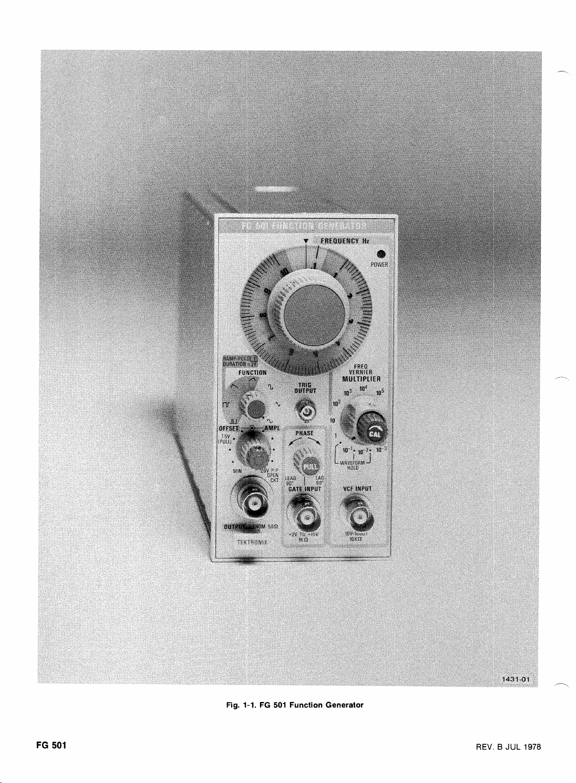
Fig.
1-1.
FG
501
Function Generator
REV.
B
JUL
1978
Page 5
INSTRUCTIONS
Section
1-FG
501
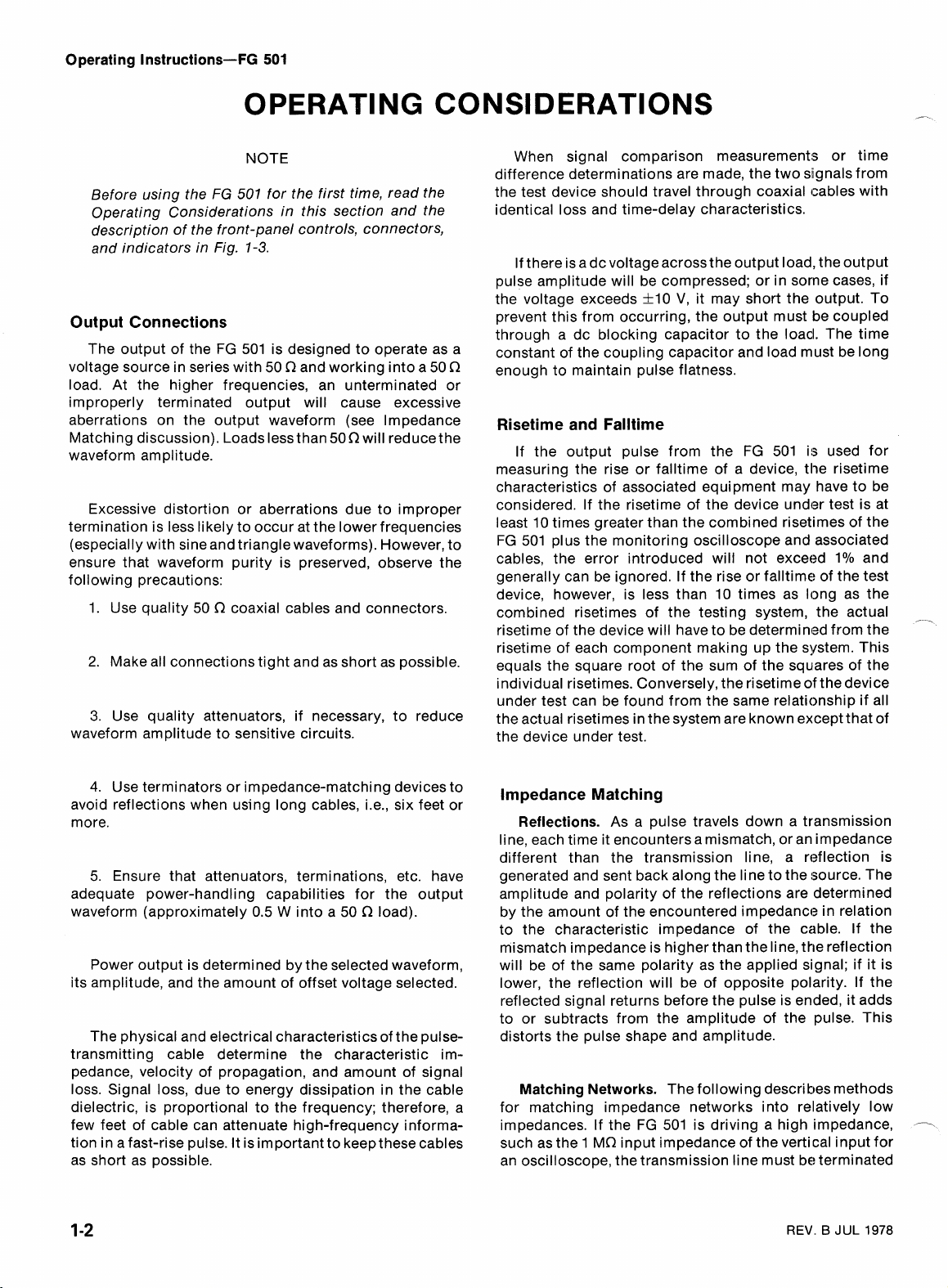
INTRODUCTION
The FG !501 Function Generator is designed to operate
TM
in a
square, tria~ngle, pulse, and ramp waveformsfrom 0.001
to 1
available at the front panel. Variable DC offset of k7.5 volts
is also provided. A "hold1' feature allows the generator
output to be abruptly halted at its instantaneous voltage
level and held there until manually switched on again.
to control the output frequency from an external voltage
source. The output frequency can be swept above or
below the selected frequency to a maximum of
depending on the polarity and amplitude of the VCF input
and the selected output frequency.
generator to be turned on for the duration of an externally
applied gating signal. This mode provides either a single
cycle output or a train (burst) of preselected waveforms
depending on the gating signal width and the generator
frequency setting. The phase (start level) of the waveform
burst can be varied
500-Series power module. Low distortion sine,
Hz
MHz
as well as a $2.5 volt square-wave trigger are
A voltage-controlled frequency (VCF) input is provided
1000:l
Also included is an external gate input that allows the
k90°
by a front-panel control.
Installation and Removal
CAUTION
D
Turn the power module off before inserting the plugin; otherwise, damage may occur to the plug-in
circuitry. Because of the high current drawn by the
507,
FG
module be turned off before removing the FG
Refer to Fig.
barriers on the interconnecting jack of the selected
power module compartment match the cut-outs in
the
Align the FG 501 chassis with the upper and lower
guides of the selected compartment. Push the module in
and press firmly to seat the circuit board in the interconnecting jack.
Pull the Power switch on the front panel of the power
module to apply power to the FG 501. Observe that the
POWER indicator light on the FG 501 comes on.
Remove the FG 501 from the power module by pulling
the release latch at the bottom of the front panel and
sliding the unit straight out of the power module.
it is also recommended that the power
7-2.
FG
Check
501
circuit board edge connector.
to
see that the plastic
507.
The variety of swept and modulated signals available
from the IFG 501 make it especially useful for such
applications as testing servo-system or amplifier
response, distortion, and stability; FM generation and
frequency multiplication; or simply used as a variable
beat-f requency oscillator, repetition-rate, or tone- burst
generator. 'The square-wave trigger output can be used as
a source for transistor-transistor logic (TTL) or to synchronize
counter.
received. It is designed to operate in any compartment of
TM 500-Series power module only. Refer to the power
module Instruction Manual for line voltage requirements
-
and power module operation.
REV. C JUL
an external device such as an oscilloscope
The FG 501 is calibrated and ready for use when
1978
or
Interconnecting Jack
Bottom Groove
a
Fig.
1-2.
Plug-in installation and removal.
Page 6
Operating Instructions-FG
501
OPERATING CONSIDERATIONS
NOTE
Before using the
Operating Considerations in this section and the
description of the front-panel controls, connectors,
and indicators in Fig.
FG
501
for the first time, read the
1-3.
Output Connections
The output of the FG 501 is designed to operate as a
voltage source in series with 50
load. At the higher frequencies, an unterminated or
improperly terminated output will cause excessive
aberrations on the output waveform (see lmpedance
Matching discussion). Loads less than
waveform amplitude.
Excessive distortion or aberrations due to improper
termination is less likely to occur at the lower frequencies
(especially with sine and triangle waveforms). However, to
ensure that waveform purity is preserved, observe the
following precautions:
1. Use quality 50
2.
Make all connections tight and as short as possible.
3.
Use quality attenuators, if necessary, to reduce
waveform amplitude to sensitive circuits.
f2
coaxial cables and connectors.
f2
and working into a 50
50 R will reduce the
f2
When signal comparison measurements or time
difference determinations are made, the two siignals from
the test device should travel through coaxial cables with
identical loss and time-delay characteristics.
If there is a dc voltage across the output load, the output
pulse amplitude will be compressed; or in sorne cases, if
the voltage exceeds
prevent this from occurring, the output must be coupled
through a dc blocking capacitor to the load. The time
constant of the coupling capacitor and load must be long
enough to maintain pulse flatness.
f
10
V,
it may short the output. To
Risetime and Falltime
If the output pulse from the FG 501 is used for
measuring the rise or falltime of a device, the risetime
characteristics of associated equipment may have to be
considered. If the risetime of the device under test is at
least 10 times greater than the combined risetimes of the
FG 501 plus the monitoring oscilloscope and associated
cables, the error introduced will not exceed 1% and
generally can be ignored. If the rise or falltime of the test
device, however,
combined
risetime of the device will have to be determined from the
risetime of each component making up the system. This
equals the square root of the sum of the squares of the
individual risetimes. Conversely, the
under test can be found from the same relationship if all
the actual risetimes in the system are known except that of
the device under test.
risetimes of the testing system, the actual
is less than 10 times as long as the
risetime of the device
/-
4. Use terminators or impedance-matching devices to
avoid reflections when using long cables, i.e., six feet or
more.
5. Ensure that attenuators, terminations, etc. have
adequate power-handling capabilities for the output
waveform (approximately 0.5 W into a 50
Power output is determined by the selected waveform,
its amplitude, and the amount of offset voltage selected.
The physical and electrical characteristics of the pulse-
transmitting cable determine the characteristic im-
pedance, velocity of propagation, and amount of signal
loss. Signal loss, due to energy dissipation in the cable
dielectric, is proportional to the frequency; therefore, a
few feet of cable can attenuate high-frequency information in a fast-rise pulse. It is important to keep these cables
as short as possible.
f2
load).
lmpedance Matching
Reflections.
line, each time it encounters a mismatch, or an impedance
different than the transmission line, a reflection is
generated and sent back along the line to the source. The
amplitude and polarity of the reflections are determined
by the amount of the encountered impedance in relation
to the characteristic impedance of the cable. If the
mismatch impedance is higher than the line, the reflection
will be of the same polarity as the applied signal; if it is
lower, the reflection will be of opposite polarity. If the
reflected signal returns before the pulse is ended, it adds
to or subtracts from the amplitude of the pulse. This
distorts the pulse shape and amplitude.
Matching Networks.
for matching impedance networks into relatively low
impedances. If the FG 501 is driving a high impedance,
such as the 1 MR input impedance of the vertical input for
an oscilloscope, the transmission line must be terminated
As a pulse travels down a transmission
The following describes methods
REV.
B
JUL
1978
--
Page 7
Operating Instructions-FG
501
REV
C,
MAR
1979
Fig.
1-3.
Operating controls and connectors.
Page 8
Operating Instructions-FG
501
into a 50
oscilloscope input. The attenuator isolates the input
capacity of the device. Distortion can be caused by this
input capacity.
A simple resistive impedance-matching network that
provides minimum attenuation is illustrated in Fig. 1-4. To
match impedance with the illustrated network, the follow-
ing conditions must exist:
and
Theref ore:
For example; to match a 50
Z1 equals 50
f2
attenuator and a 50
+
Z2)R2 must equal
(R1
Ri + Z2+ R2
RI
+
-
'IR2
ZI + R2
R1R2
=
2122; and RIZl = R2(Z2 - Z1)
Cl
and Z2 equals 125
f2
termination at the
must equal
f2
system to a 125
0.
zI
~2
f2
system,
Zl
-
(Low)
Fig.
1-4.
attenuation.
(22) encounters a greater voltage attenuation
greater than 1 and less than 2 (Z~IZI):
Impedance-matching network that provides minimum
A signal (E2) applied from the higher impedance source
-
(A2)
(High)
which is
2
Theref ore:
1
and R2
When constructing such a device, the environment
surrounding the components should also be designed to
provide a transition between the impedances. Keep in
mind that the characteristic impedance of a coaxial device
is determined by the ratio between the outside diameter of
the inner conductor to the inside diameter of the outer
z,
conductor.
diameter of the outer conductor, and d is the outside
diameter of the inner conductor. E is the dielectric constant (1 in air).
Attenuation Ratios.
provides minimum attenuation for a purely resistive
impedance-matching device, the attenuation as seen from
one end does not equal that seen from the other end.
signal (El) applied from the lower impedance source (Z1)
encounters a voltage attenuation (A1) which is greater
than 1 and less than
=
50dT 125 - 50 = 64.6
1381
E
loglo Dld, where D is the inside
Though the network in Fig. 1-4
2,
as follows:
f2
A
In the example of matching 50
The illustrated
different attenuation ratios by adding
(less than R1) between Z1 and the junction of R1 and R2.
network can be modified to provide
f2
to 125
anot.her resistor
f2.
Duration of Ramps and Pulses
The duration of ramp and pulse waveforrns is always
equal to the half-cycle time of the sine, square, or triangle
waveform frequency. For MULTIPLIER setti~ngs of 1 or
greater, the
a
duty cycle of approximately 80°/o, i.e., frequency equals
approximately 1.6X FREQUENCY
MULTIPLIER settings less than 1, the retrace/off time is
from 10 ms to 100 ms, which results in duty cycles
approaching 10O0/0; i.e., frequency equals approximately
2X FREQUENCY
retraceloff time is such that the waveform has
Hz
dial setting. For
Hz
dial setting.
---
REV.
B
JUL
1978
Page 9
OPERATION
Operating Instructions-FG
501
Free-Running Output
-A
The following procedure provides a free-running
waveform output with variable frequency and amplitude.
1. Set the AMPL control to the fully counterclockwise
position and the OFFSET control to the 0 (centered)
position. Check that the PHASE control is pushed in (off).
2.
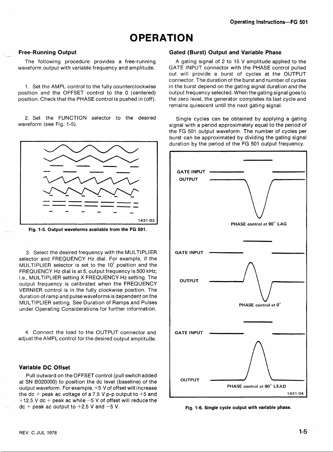
Set the FUNCTION selector to the desired
waveform (see Fig. 1-5).
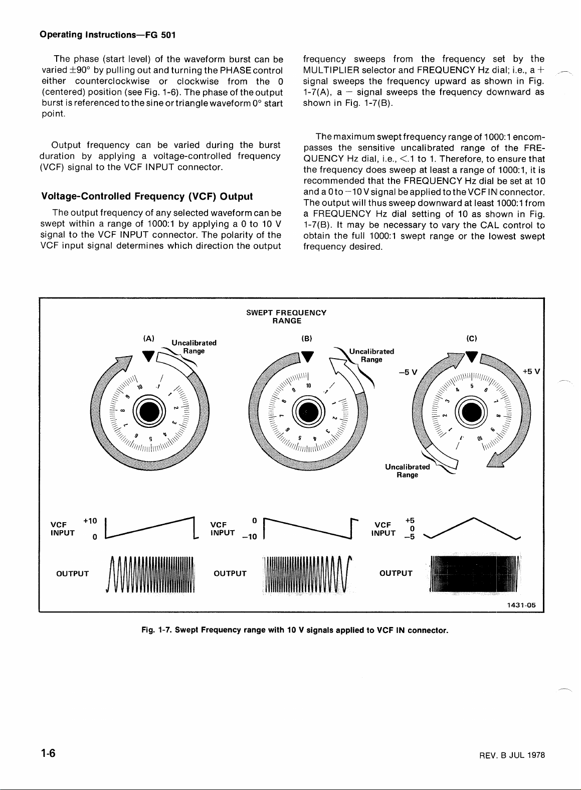
Gated (Burst) Output and Variable Phase
A gating signal of 2 to 15 V amplitude applied to the
GATE INPUT connector with the PHASE control pulled
out will provide a burst of cycles at the OUTPUT
connector. The duration of the burst and number of cycles
in the burst depend on the gating signal duration and the
output frequency selected. When the gating signal goes to
the zero level, the generator completes its last cycle and
remains quiescent until the next gating signal.
Single cycles can be obtained by applying a gating
signal with a period approximately equal to the period of
the FG 501 output waveform. The number of cycles per
burst can be approximated by dividing the gating signal
duration by the period of the FG 501 output frequency
GATE INPUT
Fig.
1-5.
Output waveforms available from the
3.
Select the desired frequency with the MULTIPLIER
FG
501.
selector and FREQUENCY Hz dial. For example, if the
lo5
MULTIPLIER selector is set to the
position and the
FREQUENCY Hz dial is at 5, output frequency is 500 kHz;
X
i.e., MULTIPLIER setting
FREQUENCY Hz setting. The
output frequency is calibrated when the FREQUENCY
VERNIER control is in the fully clockwise position. The
duration of ramp and pulse waveforms is dependent on the
MULTIPLIER setting. See Duration of Ramps and Pulses
under Operating Considerations for further information.
4.
Connect the load to the OUTPUT connector and
adjust the AMPL control for the desired output amplituae.
Variable
DC
Offset
Pull outward on the OFFSETcontrol (pull switch added
at SN B020000) to position the dc level (baseline) of the
V
output waveform. For example,
+
the dc
+
12.5 V dc
dc
peak ac voltage of a 7.5 V p-p output to +5 and
.t
peak ac while -5 V of offset will reduce the
+
peak ac output to +2.5 V and -5
of offset will increase
$5
V.
GATE INPUT
GATE INPUT
Fig.
1-6.
control at
PHASE
PHASE
PHASE
control at
Single cycle output with variable phase.
90"
control at
90"
LAG
0"
LEAD
1
43
1
-04
REV.
C
JUL
'1978
Page 10
Operating Instructions-FG
501
The phase (start level) of the waveform burst can be
varied +90° by pulling out and turning the PHASEcontrol
either counterclockwise or clockwise from the 0
(centered) position (see Fig. 1-6). The phase of theoutput
burst is referenced to the sine or triangle waveform 0° start
point.
Output frequency can be varied during the burst
duration by
applying a voltage-controlled frequency
(VCF) signal to the VCF INPUT connector.
Voltage-Controlled Frequency (VCF) Output
The output frequency of any selected waveform can be
swept within a range of 1000:l by applying a 0 to 10 V
signal to the VCF INPUT connector. The polarity of the
VCF input signal determines which direction the output
SWEPT FREQUENCY
RANGE
(A) Uncalibrated
frequency sweeps from the frequency
MULTIPLIER selector and FREQUENCY Hz dial; i.e., a
slet by the
+
signal sweeps the frequency upward as shown in Fig.
-
1-7(A), a
signal sweeps the frequency doiwnward as
shown in Fig. 1-7(B).
The maximum swept frequency range of 1000: 1 encompasses the sensitive uncalibrated range of the FREQUENCY Hz dial, i.e., <.l to 1. Therefore, to ensure that
the frequency does sweep at least a range of 1000:1, it is
recommended that the FREQUENCY Hz dial be set at 10
IN1
and a Oto -1OVsignal beapplied to theVCF
connector.
The output will thus sweep downward at least 1000:l from
a FREQUENCY Hz dial setting of 10 as shown in Fig.
1-7(B). It may be necessary to vary the CAL control to
obtain the full 1000:l swept range or the lowest swept
frequency desired.
,-,
VCF
INPUT INPUT
OUTPUT OUTPUT OUTPUT
Fig.
1-7.
Swept Frequency range with
10
V signals applied to VCF
INPUT
-5
IN
connector.
REV.
B
JUL
1978
Page 11
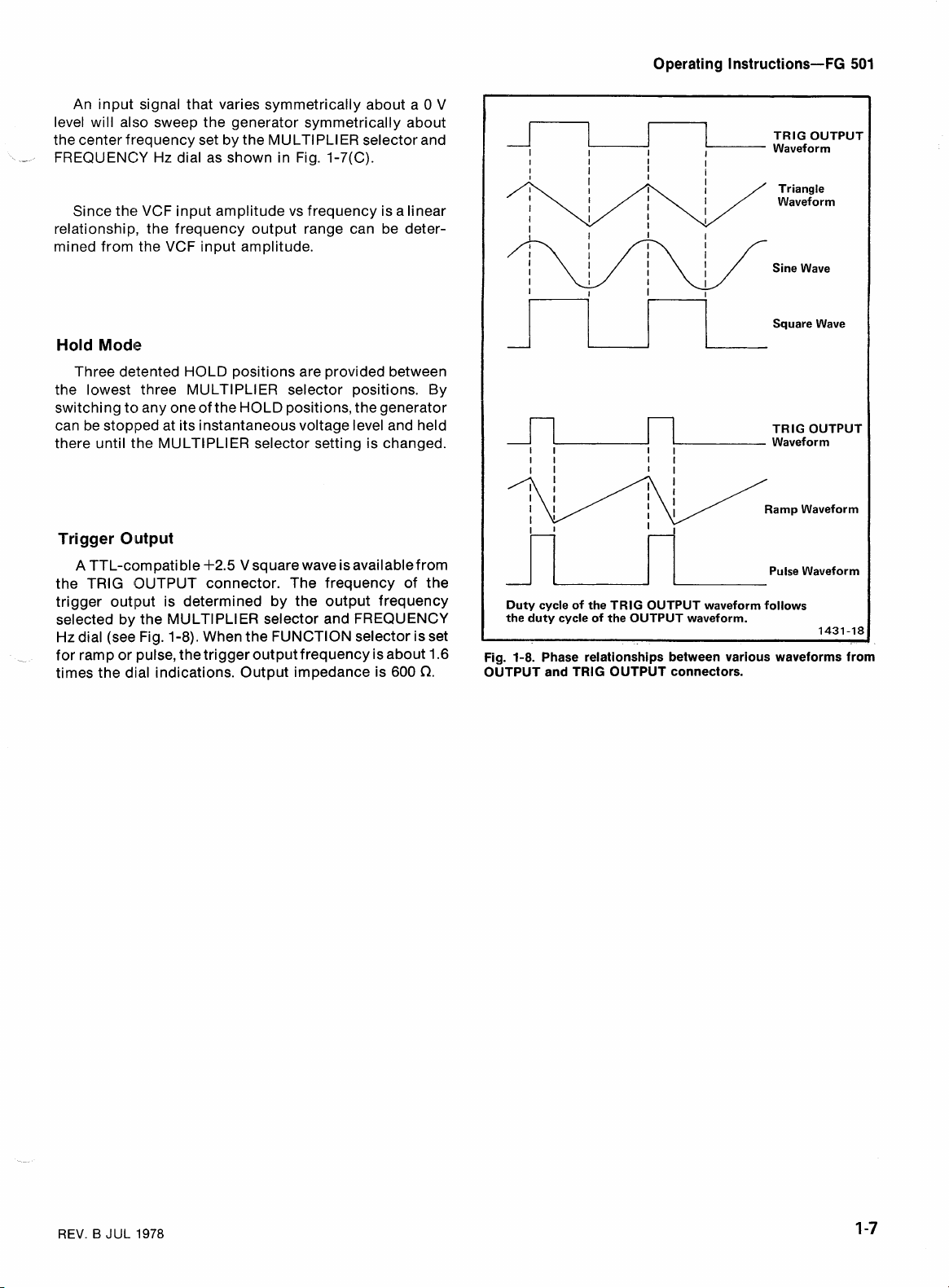
An input signal that varies symmetrically about a 0 V
level will also sweep the generator symmetrically about
the center frequency set by the MULTIPLIER selector and
-
FREQUENCY Hz dial as shown in Fig. 1-7(C).
Since the VCF input amplitude vs frequency is a linear
relationship, the frequency output range can be determined from the VCF input amplitude.
Operating Instructions-FG
Triangle
Waveform
I
I
I
I
I
I
I
Sine Wave
501
Hold
Mode
Three detented HOLD positions are provided between
the lowest three MULTl PLl ER selector positions. By
switching to any one of the HOLD positions, the generator
can be stop~ped at its instantaneous voltage level and held
there until the MULTIPLIER selector setting is changed.
Trigger
Olutput
A
TTL-corn pati
ble
+
2.5
V square wave is available from
the TRlG (OUTPUT connector. The frequency of the
trigger
outlput is determined by the output frequency
selected by the MULTIPLIER selector and FREQUENCY
Hz dial (see Fig. 1-8). When the FUNCTION selector is set
for ramp or pulse, the trigger output frequency
.
times the dial indications. Output impedance is 600
is
about 1.6
n.
I
I
I
Duty cycle of the TRlG OUTPUT waveform follows
the duty cycle of the OUTPUT waveform.
Fig. 1-8. Phase relationships between various waveforms from
OUTPUT
and
TRlG OUTPUT
I
I
connectors.
Square Wave
lG
OUTPUT
TR
Waveform
Ramp Waveform
1431-18
REV. B JUL
1978
Page 12
Operating Instructions-FG 501
APPLICATIONS
Response
The FG 501 is particularly suited for determining
response characteristics of circuits or systems. This
application utilizes the VCF input of the FG 501 to sweep
the generator over a range of frequencies. By applying the
desired waveform from another FG 501 (or equivalent) to a
device under test and sweeping the waveform frequency
over a selected range, various response characteristics
can be observed on a monitoring oscilloscope.
The following procedure describes a technique for
determining response characteristics of any
sensitive device that operates within the frequency range
of the FG 501. Refer to the Voltage-Controlled Frequency
(VCF) Output discussion under Operation for additional
information.
1. Connect the equipment as shown in Fig. 1-9.
2.
dial for the desired upper or lower frequency limit
(depending on the direction you wish to sweep).
Analysis
frequency-
Set the MULTl PLl ER selector and FREQUENCY Hz
3.
Apply the desired waveform to the VCF INPUT
connector. (A positive-going waveform will sweep the
frequency upwards from the FREQUENCY Hz dial setting
while a negative-going waveform will sweep clownwards.
4.
Adjust the amplitude of the VCF input waveform for
the desired output frequency range.
5. Observe the response characteristics on the
monitori ng oscilloscope.
The frequency at whi
characteristic occurs can be determined by first removing
the VCF input waveform, then manually adljusting the
FREQUENCY Hz dial to again obtain the particular
characteristic observed in the swept display and reading
that frequency on the FREQUENCY Hz dial.
splayed respon
WAVEFORM
Fig.
I
,
1-9.
Analyzing circuit or system response.
UNDER
TEST
1
REV. B JUL
1978
Page 13
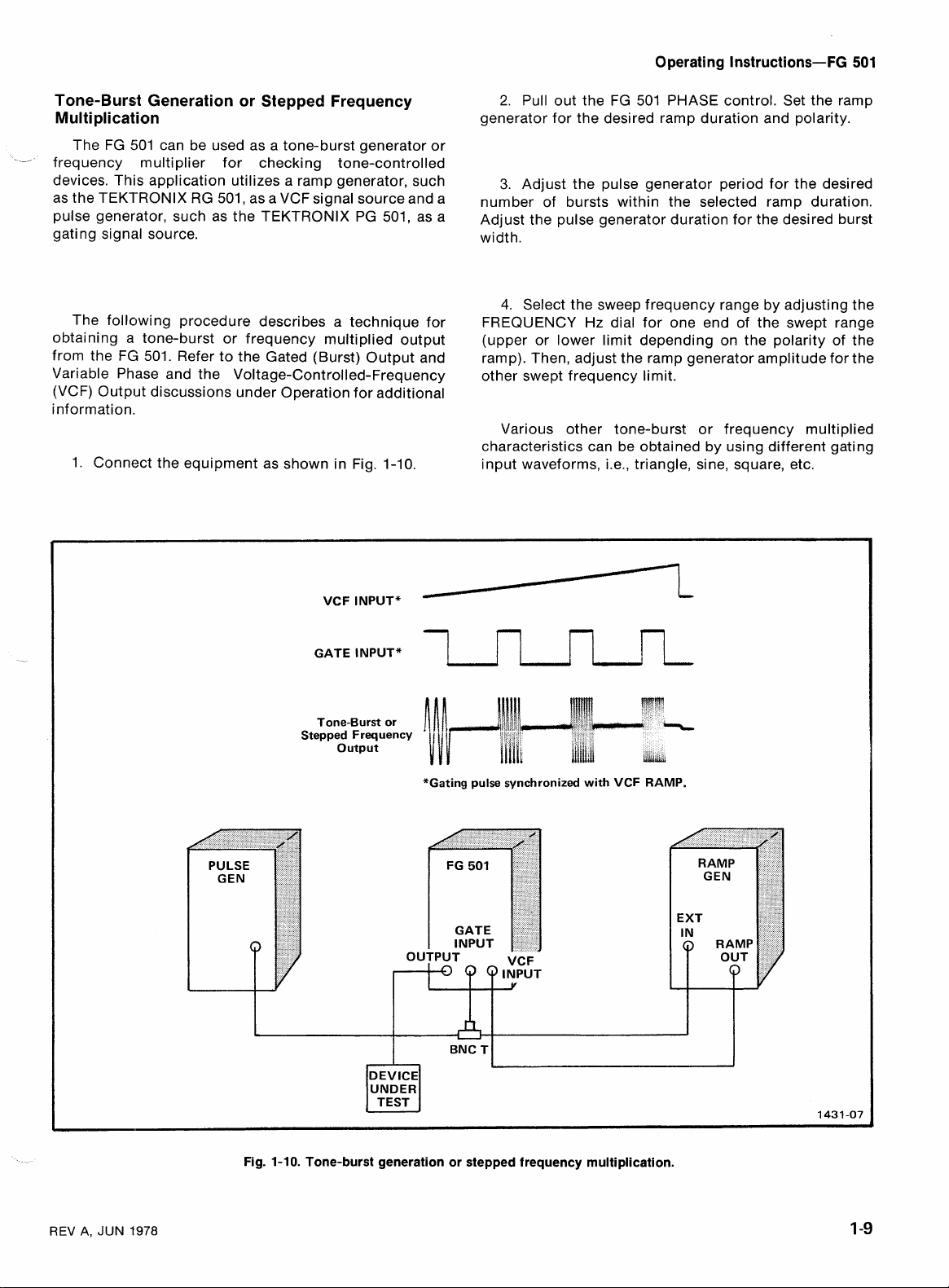
Tone-Burst Generation or Stepped Frequency
Multiplication
\
._
The FG 501 can be used as a tone-burst generator or
frequency multiplier for checking tone-controlled
devices. This application utilizes a ramp generator, such
as the TEKTRONIX RG 501, as a VCF signal source and a
pulse generator, such as the TEKTRONIX PG 501, as a
gating signal source.
Operating Instructions-FG
2.
Pull out the FG 501 PHASE control. Set the ramp
501
generator for the desired ramp duration and polarity.
3.
Adjust the pulse generator period for the desired
number of bursts within the selected ramp duration.
Adjust the pulse generator duration for the desired burst
width.
The following procedure describes a technique for
obtaining a tone-burst or frequency multiplied output
from the FG 501. Refer to the Gated (Burst) Output and
Variable Phase and the Voltage-Controlled-Frequency
(VCF) Output discussions under Operation for additional
information.
1. Connect the equipment as shown in Fig. 1-10.
VCF INPUT*
GATE INPUT*
Tone-Burst or
Stepped Frequency
Output
4. Select the sweep frequency range by adjusting the
Hz
FREQUENCY
dial for one end of the swept range
(upper or lower limit depending on the polarity of the
ramp). Then, adjust the ramp generator amplitude for the
other swept frequency limit.
Various other tone-burst or frequency multiplied
characteristics can be obtained by using different gating
input waveforms, i.e., triangle, sine, square, etc.
UUUL
REV
A,
JUN
1978
PULSE
GEN
Fig.
*Gating pulse synchronized with VCF RAMP.
DEVICE
UNDER
1-10.
Tone-burst generation or stepped frequency multiplication.
Page 14

Page 15
Section
SPECIFICATION
AND PERFORMANCE CHECK
SPECIFICATION
2-FG
501
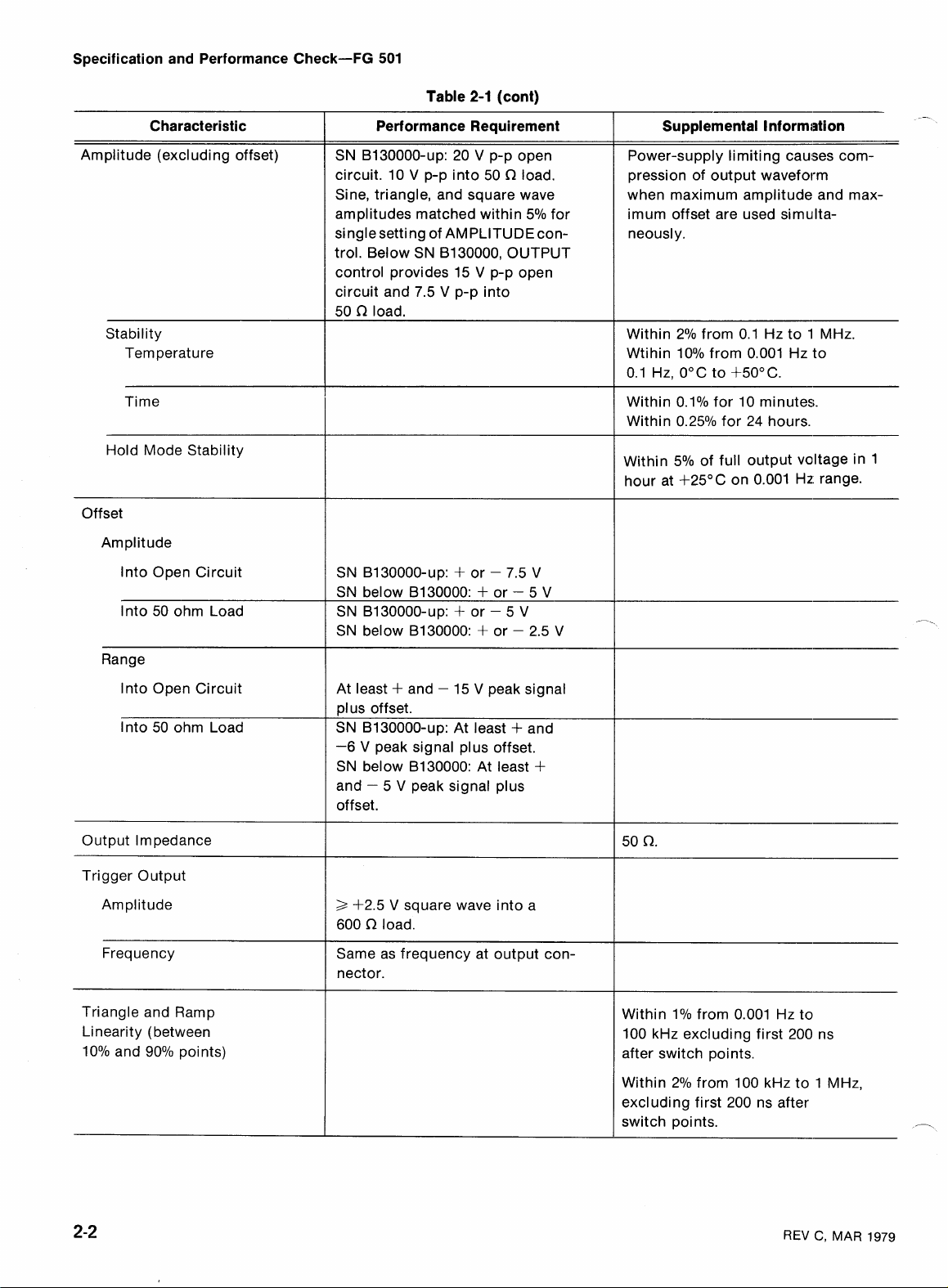
Performar~ce Conditions
The electrical characteristics are valid only if the
FG 501 has been calibrated at an ambient temperature
between +20° C and +30° C and is operating at an ambient
tem perature between 0" C and +50° C unless otherwise
noted. Forced air circulation is required for ambient
tem
perat ure above 4-40' C.
Table
ELECTRICAL CHARACTERISTICS
Characteristic
Frequency
Range
Sine VVave, Square Wave,
and Tiriangle
Accuracy
Resolution
--
Performance Requirement
0.01
Hz
to 1
Within 3% of full scale 1 to 10;
.1 to 1 uncalibrated.
-
MHz
in 9 decade steps.
Only those items listed in the Performance Requirements column of the Electrical Characteristics table
are normally verified when doing the Performance Check
procedure of this manual. Items listed in the Supplemental
lnformation column are either explanatory notes or
minimum performance characteristics for which no
tolerance ranges are specified, and which normally re-
quire verification only after repairs or parts replacement.
2-1
--
-
Supplemental lnformation
1 part in
FREQUENCY VERNl ER control.
lo4
of full scale with
Stability
Tem perature
Time
Pulse and Ramp range
Time
Symmetry
Sine Wave, Square Wave,
and Triangle
REV.
6
JUL
'1978
Within 1% from 0.001
on calibrated portion (1 to 10)
of FREQUENCY
+50° C.
Hz
to 1 MHz
Hz
dial, +20°C to
Within 2% from 0.1
and within 10% from 0.001
Hz,
0.1
Within 0.1% for 10 minutes.
Within 0.25% for 24 hours.
=2X dial setting with MULTI-
PLIER at
ting with MULTIPLIER AT
setting.
Within 10% on uncalibrated portion (0.1 to 1) of FREQUENCY
dial.
0° C to +SO0 C.
Hz
to 1 MHz,
Hz
to +.6X dial set-
lo5
to
Hz
Page 16
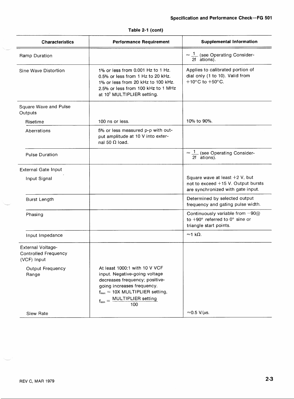
Specification and Performance Check-FG
Characteristic
501
Table
2-1
(cont)
Performance Requirement
Supplemental I nformiation
--
Amplitude (excluding offset)
Stability
Temperature
Time
Hold Mode Stability
Offset
Amplitude
Into Open Circuit
Into 50 ohm Load
SN B130000-up: 20 V p-p open
V
circuit. 10
Sine, triangle, and square wave
amplitudes matched within
single setting of AMPLlTUDEcontrol. Below SN B130000, OUTPUT
control provides 15
circuit and 7.5
fl
load.
50
SN B130000-up:
SN below 8130000: + or - 5
SN B130000-up: + or - 5
SN below B130000: + or - 2.5
p-p into 50
V
p-p into
+
fl
V
p-p open
or - 7.5
load.
5% for
V
V
V
V
Power-supply limiting causes compression of output waveform
when maximum amplitude and max-
imum offset are used
neousl y.
Within 2% from 0.1 Hz to 1 MHz.
Wtihin
0.1 Hz, 0°C to
Within 0.1% for 10 minutes.
Within 0.25% for 24 hours.
Within 5% of full output voltage in 1
hour at +25OC on 0.001
10% from 0.001 Hz to
+SO0
simu~lta-
C.
Hz:
range.
Range
Into Open Circuit
Into 50 ohm Load
Output Impedance
Trigger Output
Amplitude
Frequency
Triangle and Ramp
Linearity (between
10% and 90% points)
I
At least
plus offset.
SN B130000-up: At least
-6
SN below B130000: At least
and
offset.
3
600
Same as frequency at output
nector.
+
and - 15 V peak signal
V
peak signal plus offset.
-
5 V peak signal plus
+2.5 V square wave into a
n
load.
+
and
+
con-
I
n.
50
Within
100 kHz excluding first 200 ns
after switch points.
Within
excluding first 200 ns after
switch points.
1% from 0.081 Hz to
2% from 100 kHz to 1 MHz,
-
REV
C,
MAR
1979
Page 17
Table
2-1
Specification and Performance Check-FG 501
(cont)
characteristics
-
Ramp Duration
Sine Wave Distortion
Square Wave and Pulse
Outputs
Aberrations
Pulse Dluration
External Gate lnput
lnput Signal
Performance Requirement
1% or less from 0.001 Hz to 1 Hz.
0.5% or less from 1 Hz to 20 kHz.
1% or less from 20 kHz to 100 kHz.
2.5% or less from 100 kHz to 1 MHz
at
10' MULTIPLIER setting.
100 ns or less.
5% or less measured p-p with out-
put amplitude at 10 V into exter-
0
nal 50
load.
Supplemental Information
--
(see Operating Consider-
2f ations).
Applies to calibrated portion of
dial only (1 to 10). Valid from
+lO°C to +50°C.
=
1
(see Operating Consider-
2f ations).
Square wave at least +2 V, but
not to exceed +15 V. Output bursts
are synchronized with gate input.
Burst Length
Phasing
lnput lrnpedance
External V'oltageControlled Frequency
(VCF) lnput
Output Frequency
Range
Slew Rate
At least 1000:l with 10 V VCF
input. Negative-going voltage
decreases frequency; positivegoing increases frequency.
f,,
=
10X MULTIPLIER setting,
MULTl PLl ER setting
f.
=
mln
100
Determined by selected output
frequency and gating pulse width.
Continuously variable from -90@
to +90° referred to 0° sine or
triangle start points.
REV
C,
MAR
1979
Page 18
Specification and Performance Check-FG
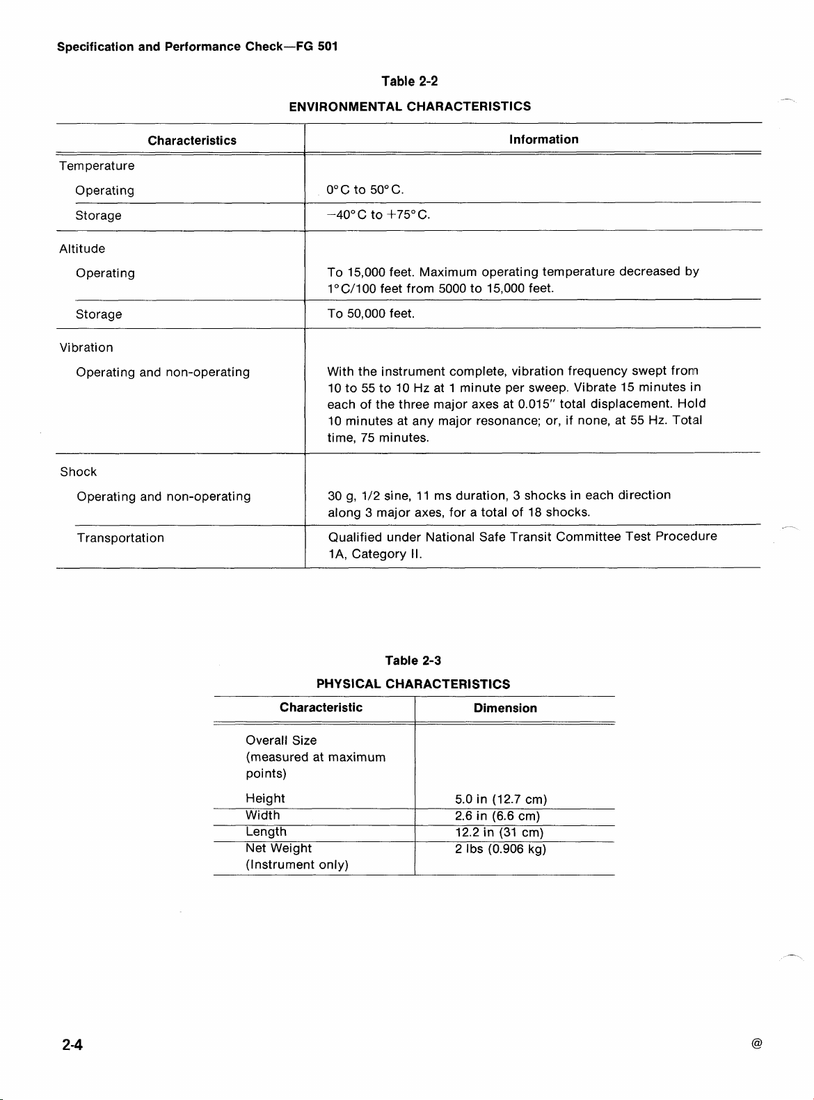
ENVIRONMENTAL CHARACTERISTICS
501
Table
2-2
Characteristics
Tern perat ure
Operating
Storage
Altitude
Operating
Storage
Vibration
Operating and non-operating
Shock
Operating and non-operating
Transportation
Information
To 15,000 feet. Maximum operating temperature decreased by
1
O
C/100 feet from 5000 to 15,000 feet.
-
To 50,000 feet.
With the instrument complete, vibration frequency swept from
10 to 55 to 10 Hz at 1 minute per sweep. Vibrate 15 minutes in
each of the three major axes at 0.015" total displacement. Holld
10 minutes at any major resonance; or, if none, at 55 Hz. Totid
time, 75 minutes.
30 g, 1/2 sine, 11 ms duration, 3 shocks in each direction
along 3 major axes, for a total of 18 shocks.
Qualified under National Safe Transit Committee Test Procedure
1A, Category
11.
-
-
PHYSICAL CHARACTERISTICS
Characteristic
Overall Size
(measured at maximum
points)
Height
Width
Length
Net Weight
(Instrument only)
Table 2-3
I
Dimension
5.0 in (12.7 cm)
2.6 in (6.6
12.2 in (31
cm)
em)
2 Ibs (0.906 kg)
Page 19
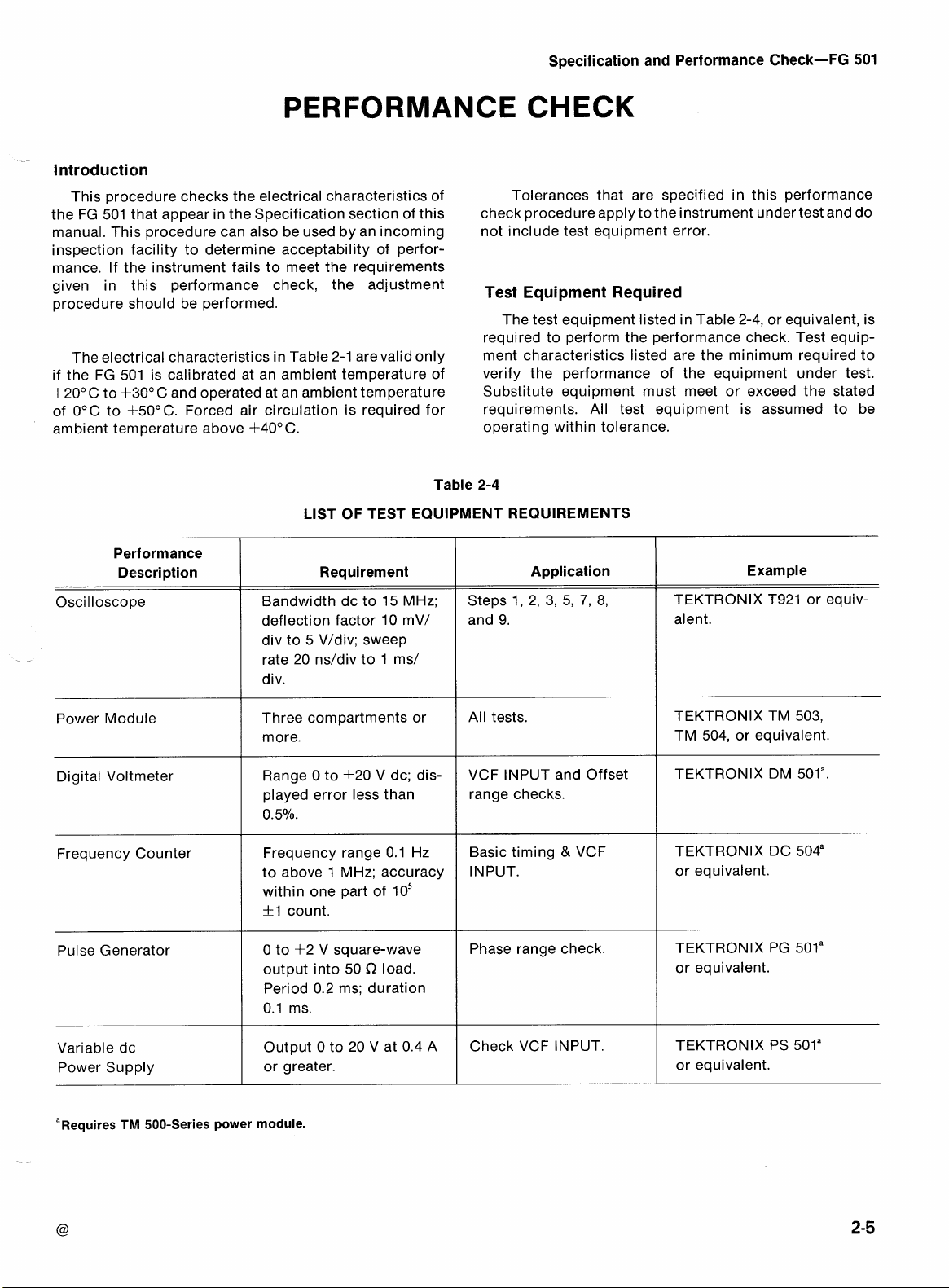
PERFORMANCE CHECK
Introduction
This procedure checks the electrical characteristics of
the FG 501 that appear in the Specification section of this
manual. Thils procedure can also be used by an incoming
inspection facility to determine acceptability of performance. If the instrument fails to meet the requirements
given in this performance check, the adjustment
procedure should be performed.
The electrical characteristics in Table 2-1
if the FG
+20°C to +:30° C and operated at an ambient temperature
of 0°C to 4-50°C. Forced air circulation is required for
ambient temperature above +40° C.
5011 is calibrated at an ambient temperature of
LIST
arevalid only
Table
OF
TEST EQUIPMENT REQUIREMENTS
Specification and Performance Check-FG
Tolerances that are specified in this performance
check procedure apply to the instrument under test and do
not include test equipment error.
Test Equipment Required
The test equipment listed in Table 2-4, or equivalent, is
required to perform the performance check. Test equipment characteristics listed are the minimum required to
verify the performance of the equipment under test.
Substitute equipment must meet or exceed the stated
requirements. All test equipment is assumed to be
operating within tolerance.
2-4
501
Performance
Description
Oscilloscope
Power Module
Digital Voltmeter
Frequency Counter
Pulse Generator
Requirement
Bandwidth dc to 15 MHz;
deflection factor 10 mV/
div to 5 V/div; sweep
rate 20 ns/div to 1 ms/
div.
Three compartments or
more.
Range 0 to +20 V dc; displayed error less than
0.5O/o.
Frequency range 0.1 Hz
to above 1 MHz; accuracy
within one part of
+1 count.
0 to +2 V square-wave
output into 50 load.
Period 0.2 ms; duration
0.1 ms.
lo5
Application
Steps 1, 2, 3,
and 9.
All tests.
VCF INPUT and Offset
range checks.
Basic timing
IN PUT.
Phase range check.
5,
&
7,
VCF
8,
Example
TEKTRONIX T921 or equivalent.
TEKTRONIX TM 503,
TM 504, or equivalent.
TEKTRONIX DM
TEKTRONIX DC 504"
or equivalent.
TEKTRONIX PG 501"
or equivalent.
501a
Variable dc
Power Supply
"~equires
Thll
Output 0 to 20 V at 0.4
or greater.
500-Series power module.
Check VCF INPUT
A
TEKTRONIX PS 501"
or equivalent.
Page 20
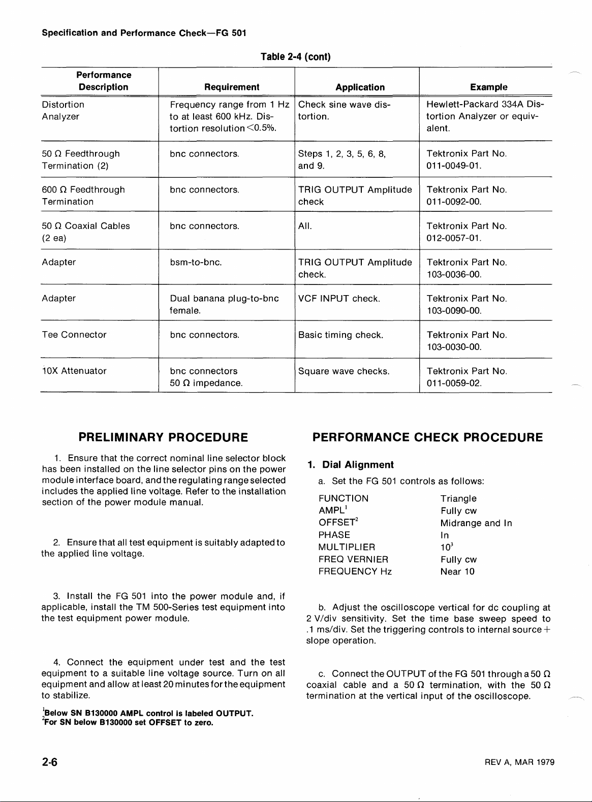
Specification and Performance Check-FG
Performance
Distortion
Analyzer
to at least 600 kHz. Distortion resolution <0.5O/o.
501
Table
2-4
(cont)
Application
Check sine wave dis-
tortion.
Example
Hewlett-Packard 334~ Distortion Analyzer or equivalent.
50
R
Feedthrough
Termination (2)
600
R
Feedt hroug h
Termination
50
R
Coaxial Cables
(2 ea)
Adapter bsm-to-bnc.
Adapter
Tee Connector
IOX
Attenuator
bnc connectors. Steps 1, 2, 3, 5, 6,
bnc connectors.
bnc connectors.
Dual banana plug-to-bnc
female.
bnc connectors.
bnc connectors
50
R
impedance.
PRELIMINARY PROCEDURE PERFORMANCE CHECK PROCEDURE
8,
and 9.
TRIG OUTPUT Amplitude
check
All.
TRIG OUTPUT Amplitude
check.
VCF INPUT check. Tektronix Part No.
Basic timing check.
Square wave checks.
Tektronix Part No.
01 1-0049-01.
Tektronix Part No.
01 1-0092-00.
Tektronix Part No.
01 2-0057-01.
Tektronix Part No.
103-0036-00.
103-0090-00.
Tektronix Part No.
103-0030-00.
Tektronix Part No.
01 1-0059-02.
1. Ensure that the correct nominal line selector block
has been installed on the line selector pins on the power
module interface board, and the regulating range selected
includes the applied line voltage. Refer to the installation
section of the power module manual.
2. Ensure that all test equipment is suitably adapted to
the applied line voltage.
3.
Install the FG 501 into the power module and, if
applicable, install the TM 500-Series test equipment into
the test equipment power module.
4. Connect the equipment under test and the test
equipment to a suitable line voltage source. Turn on all
equipment and allow at least 20 minutes for the equipment
to stabilize.
mi el ow
SN
2~or SN below
B130000
AMPL control is labeled OUTPUT.
B130000
set OFFSET to zero.
1.
Dial Alignment
a. Set the FG 501 controls as follows:
FUNCTION Triangle
AMPL'
OFFSET^
PHASE
MULTIPLIER 1
FREQ VERNIER Fully cw
FREQUENCY Hz Near 10
b. Adjust the oscilloscope vertical for dc coupling at
2 V/div sensitivity. Set the time base sweep speed to
.1 ms/div. Set the triggering controls to internad source+
slope operation.
c. Connect the OUTPUT of the FG 501 through a 50
coaxial cable and a 50 R termination, with the 50
termination at the vertical input of the oscilloscope.
FUIIY
cw
Midrange and In
In
o3
R
R
-
REV
A,
MAR
1979
Page 21
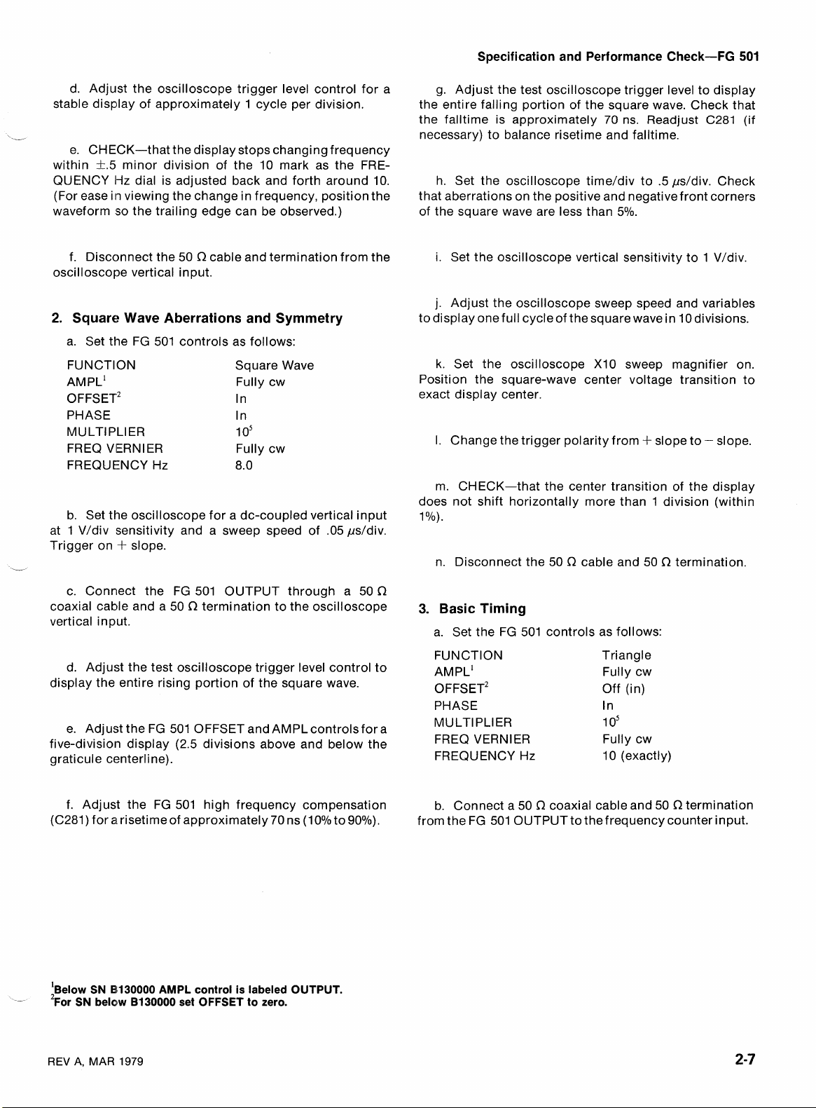
Specification and Performance Check-FG
501
\---
d. Adjust the oscilloscope trigger level control for a
stable display of approximately 1 cycle per division.
e. CHECK-that the display stops changing frequency
within k.5 minor division of the 10 mark as the FREQUENCY Hz dial is adjusted back and forth around 10.
(For ease in viewing the change in frequency, position the
waveform :so the trailing edge can be observed.)
f. Disconnect the 50
oscilloscope vertical input.
2.
Square Wave Aberrations and Symmetry
a. Set the FG 501 controls as follows:
FUNCTION
AMPL'
OFFSET'^
PHASE
MULTIPLIER
FREQ VIERNIER Fully cw
FREQUEINCY Hz 8.0
b. Set the oscilloscope for a dc-coupled vertical input
at 1 V/div sensitivity and a sweep speed of .05 pddiv.
Trigger on
+
slope.
R
cable and termination from the
Square Wave
FUIIY
cw
In
In
I
o5
g. Adjust the test oscilloscope trigger level to display
the entire falling portion of the square wave. Check that
the
falltime is approximately 70 ns. Readjust
necessary) to balance risetime and falltime.
h. Set the oscilloscope
that aberrations on the positive and negative front corners
of the square wave are less than 5%.
i. Set the oscilloscope vertical sensitivity to 1 V/div.
j. Adjust the oscilloscope sweep speed and variables
to display one full
k. Set the oscilloscope
Position the square-wave center voltage transition to
exact display center.
I. Change the trigger polarity from
m. CHECK-that the center transition of the display
does not shift horizontally more than 1 division (within
1
O/o)
.
n. Disconnect the 50 R cable and 50 R termination.
cycleof the square wave in 10 divisions.
time/div to .5 ps/div. Check
XI0 sweep magnifier on.
f
slope to - slope.
C281
(if
c. Connect the FG 501 OUTPUT through a 50
coaxial cable and a 50 R termination to the oscilloscope
vertical input.
d. Adjust the test oscilloscope trigger level control to
display the entire rising portion of the square wave.
e. Adjust the FG 501 OFFSET and AMPL controlsfor a
five-division display (2.5 divisions above and below the
graticule centerline).
f. Adjust the FG 501 high frequency compensation b. Connect a 50
ai
(C281) for
th el ow
-
2~or SN belajw B130000 set OFFSET to zero.
risetime of approximately 70 ns (10% to 90%).
SN 81130000 AMPL control
is
labeled OUTPUT.
R
3.
Basic Timing
a. Set the FG 501 controls as follows:
FUNCTION Triangle
AMPL'
OFFSET^
PHASE
MULTIPLIER 1
FREQ VERNIER Fully cw
FREQUENCY Hz 10 (exactly)
R
coaxial cable and 50 R termination
from the FG 501 OUTPUT to the frequency counter input.
FUIIY
cw
Off (i n)
In
o5
REV A, MAR
1979
Page 22
Specification and Performance Check-FG 501
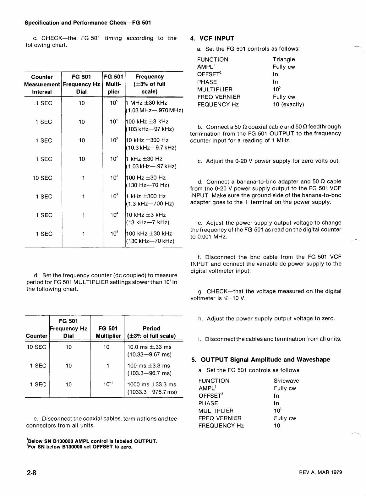
c. CHECK-the FG 501
following chart.
Counter
Measurement
Interval
.1 SEC
1 SEC
1 SEC
1 SEC
10 SEC
1 SEC
1 SEC
1 SEC
FG 501
=requency
Dial
10
timing according to the
Frequency
(f
3%
of full
scale)
1 MHz +30 kHz
(1 .O3 MHz-.970 MHz)
100 kHz f3 kHz
(103 kHz-97 kHz)
10 kHz +300 Hz
(1 0.3 kHz-9.7 kHz)
1 kHz h3O Hz
(1 .O3 kHz-.97 kHz)
100 Hz +30 Hz
(130 HZ-70 HZ)
1 kHz +300 Hz
(1.3 kHz-700 HZ)
pi!;z:7 ZZ)
100 kHz +30 kHz
(130 kHz-70 kHz)
Hz
FG 501
Multi-
plier
1
o5
1
o4
1
o3
1 02
1
o2
1
o3
1
o4
1
o5
4.
VCF
INPUT
a. Set the FG 501 controls as follows:
FUNCTION Triangle
AMPL'
OFFSET^
PHASE In
MULTIPLIER
FREQ VERNIER Fully cw
FEQUENCY Hz 1 0 (exactly)
C2
b. Connect a 50
termination from the FG 501 OUTPUT to the frequency
counter input for a reading of 1 MHz.
c. Adjust the 0-20 V power supply for zero volts out.
d. Connect a banana-to-bnc adapter and 50
from the 0-20 V power supply output to the FIG 501 VCF
INPUT. Make sure the ground side of the banana-to-bnc
adapter goes to the
e. Adjust the power supply output voltage to change
the frequency of the FG 501 as read on the digital counter
to 0.001 MHz.
coaxial cable and 50 nfeedthrough
+
terminal on the power supply.
FUIIY
In
I
o5
cw
$2
cable
d. Set the frequency counter (dc coupled) to measure
period for FG 501 MULTIPLIER settings slowerthan
the following chart.
FG 501
Hz
Frequency
Counter
10 SEC
1 SEC
1 SEC
e. Disconnect the coaxial cables, terminations and tee
connectors from all units.
Dial
FG 501
Multiplier
Period
(f
3%
of full scale)
10.0 ms k.33 ms
(1 0.33-9.67 ms)
100 ms h3.3 ms
(1
03.3-96.7 ms)
1000 ms k33.3 ms
(1 033.3-976.7 ms)
lo2
in
f. Disconnect the bnc cable from the FG 501 VCF
INPUT and connect the variable dc power supply to the
digital voltmeter input.
g. CHECK-that the voltage measured on the digital
voltmeter is <-I0 V.
h. Adjust the power supply output voltage to zero.
i.
Disconnect the cables and termination from all units.
5.
OUTPUT Signal Amplitude and Waveshape
a. Set the FG 501 controls as follows:
FUNCTION Si newave
AMPL'
OFFSET^
PHASE In
MULTIPLIER 1
FREQ VERNIER Fully cw
FREQUENCY Hz 10
FUIIY
In
o3
cw
elow ow
SN
SN
2~or
below
B130000
8130000
AMPL control is labeled OUTPUT.
set OFFSET to zero.
REV
44,
MAR
1979
Page 23
Specification and Performance Check-FG
501
b. Set the oscilloscope vertical for dc-coupling at
2
V/divsensitivity. Set the triggering controls to internal,
slope. Set the time base sweep speed to 20 ps.
R
c. Connect a 50
from the FG 501 OUTPUT to the oscilloscope vertical
input and obtain a triggered display.
d. Turn the FG 501 FUNCTION selector to each
position.
e. CHECK-that the peak-to-peak amplitude of each
output
for SN below B130000.
FUNCTION selector corresponds to that shown on the
front panel of the FG 501.
from the oscilloscope.
sign,al is 210 volts for SN B130000-up; 37.5 volts
f. CHECK-that the waveform for each position of the
Disconnect the 50
g.
6.
OFFSE'T Range
a. Set the FG 501 as follows:
coaxial cable and 50 R termination
R
termination and 50 R cable
R
+
h. Disconnect the 50
from the digital voltmeter.
7.
TRlG OUTPUT Amplitude
a. Set the FG 501 as follows:
FUNCTION Triangle
AMPL'
OFFSET^
PHASE In
MULTIPLIER 1
FREQ VERNIER Fully cw
FREQUENCY Hz 10
b. Set the oscilloscope for 1 V/div vertical sensitivity.
c. Connect a bsm-to-bnc adapter to the FG 501 TRIG
OUTPUT. Connect a 50
R
to a 600
termination to the oscilloscope vertical input. Set os-
cilloscope triggering to internal and
triggering level for a stable display.
through-signal termination. Connect the 600
cable and 50 R termination
FUIIY
cw
In
o3
R
coaxial cable from the adapter
+
R
slope. Set the
FUNCTION Triangle
-
AMPL
OFFSET OUT (SN B130000-up)
PHASE
MULTI
PL-I ER 1
FREQ VERNIER Fully cw
FREQUENCY Hz 10
b. Set the digital voltmeter to the 20 dc volts scale.
Connect the FG 501 OUTPUT with a 50
c.
cable terminated in 50
d. Adjust the FG 501 OFFSET to the fully clockwise
position.
e. CHECK-SN B130000-up for at least
below B1 30000 for at least 4-2.5 V.
f. Adjust the FG 501 OFFSET to the fully
counterclockwise position.
g. CHECK-SN B130000-up for at least -3.75 V; SN
B130000 for at least -2.5 V.
below
Fully ccw
In
o3
R
coaxial
R
at the digital multimeter input.
f3.75 V; SN
d. CHECK-for a square wave display equal to or
greater than 2.5 volts in amplitude.
R
e. Disconnect the adapter, cable, and 600
tion from both units.
8.
Sine Wave Distortion
a. Set the FG 501 controls as follows:
FUNCTION Sine wave
AMPL'
OFFSET^
PHASE In
MULTlPLl ER 10
FREQ VERNIER Fully cw
FREQUENCY Hz 10
b. If using a distortion analyzer similar to the
connect the 50
FG 501 OUTPUT connector to the distortion
input. Place
connector.
R
cable and 50 R termination
a
50 R termination on the FG 50
FUIIY
In
cw
termina-
HP 334A,
from the
analyzer
1 VCF IN
elow ow
SN B1130000
2~or SN below 8130000 set OFFSET to zero.
REV
A,
MAR
'1
979
AMPL
control
is
labeled OUTPUT.
Page 24
Specification
and
Performance Check-FG 501
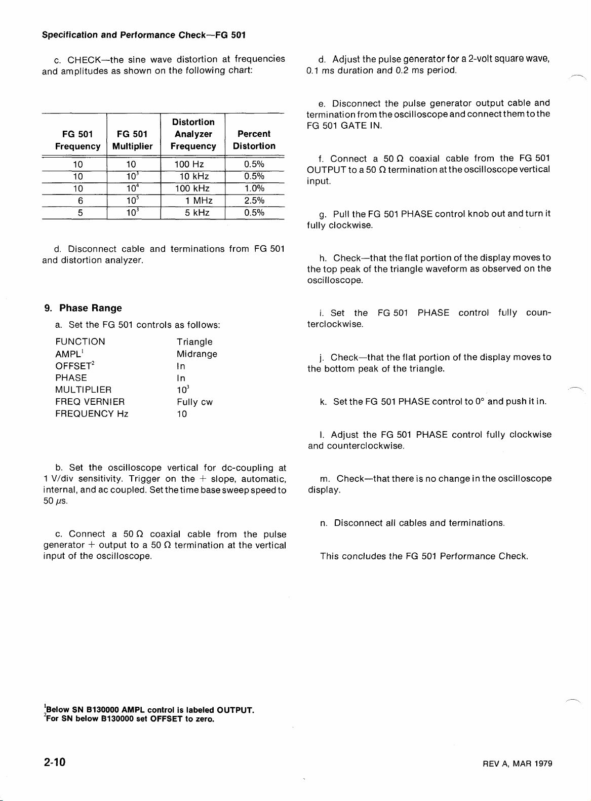
c. CHECK-the sine wave distortion at frequencies
and amplitudes as shown on the following chart:
Distortion
FG 501
Frequency
10
o5
1
o3
1
d. Disconnect cable and terminations from FG 501
and distortion analyzer.
9.
Phase Range
a. Set the FG 501 controls as follows:
FUNCTION Triangle
AMPL'
OFFSET^
PHASE In
MULTIPLIER 1
FREQ VERNIER Fully cw
FREQUENCY Hz 10
100 Hz 0.5%
10 kHz 0.5%
1 MHz 2.5%
5
HZ
Midrange
In
0.5%
o3
d. Adjust the pulse
0.1 ms duration and 0.2 ms period.
e. Disconnect the pulse generator output cable and
termination from the oscilloscopeand connect them to the
FG 501 GATE IN.
f.
Connect a 50 n coaxial cable from the FG 501
OUTPUT to a 50
input.
g. Pull the FG 501 PHASE control knob out and turn it
fully clockwise.
h. Check-that the flat portion of the display moves to
the top peak of the triangle waveform as observed on the
oscilloscope.
i. Set the FG 501 PHASE control f~~lly counterclockwise.
j. Check-that the flat portion of the display moves to
the bottom peak of the triangle.
k. Set the FG 501 PHASE control to
generator
C2
termination at t he oscilloscc~pe vertical
for
a
2-volt square wave,
0"
and push it in.
-
-
b. Set the oscilloscope vertical for dc-coupling at
+
1 V/div sensitivity. Trigger on the
internal, and ac coupled. Set the time basesweep speed to
50 /IS.
C2
c. Connect a 50
+
generator
input of the oscilloscope.
e el ow
2~or SN below B130000 set OFFSET to zero.
output to a 50 Q termination at the vertical
SN 8130000
coaxial cable from the pulse
AMPL
control
is
slope, automatic,
labeled OUTPUT.
I. Adjust the FG 501 PHASE control fully clockwise
and counterclockwise.
m. Check-that there is no change in the o:~cilloscope
display.
n. Disconnect all cables and terminations.
This concludes the FG 501 Performance Check.
REV
A,
MAR
1979
Page 25

WARNING
THE FOLLOWING SERVICING INSTRUCTIONS ARE
FOR USE BY QUALIFIED PERSONNEL ONLY. TO
AVOID PERSONAL INJURY, DO NOT PERFORM ANY
SERVICING OTHER THAN THAT CONTAINED IN
OPERATING INSTRUCTIONS UNLESS YOU ARE
QUALIFIED TO DO SO.
Page 26

Page 27

ADJUSTMENT
Section
3-FG
501
Introduction
This adjustment procedure is to be used to restore the
FG 501 to original performance specifications. Adjustment need not be performed unless the instrument failsto
meet the Performance Requirements of the Electrical
Characteristics listed in the Specification section, or the
Performance Check cannot be completed satisfactorily.
Completion of all adjustment steps in this procedure
ensures that the instrument will meet the performance
requirements listed in the Specification section. However,
to fully ensulre satisfactory performance, it is recommended that the Performance Check be performed after any
adjustment is made.
Services Available
Tektronir:, I nc. provides complete instrument repair
and adjustment at local Field Service Centers and at the
Factory
Office or representative for further information.
Servicecenter. Contact your local Tektronix Field
Table
Recali bration Interval
Recommended recali bration interval is 2000 hours of
operation or six months, whichever occurs first.
Test Equipment Required
The test equipment listed in Table 3-1, or equivalent, is
required for adjustment of the FG 501. Specifications
given for the test equipment are the minimum necessary
for accurate adjustment and measurement. All test equip-
ment is assumed to be correctly calibrated and operating
within specification.
If other test equipment is substituted, control settings
or calibration setup may need to be altered to meet the
requirements of the equipment used.
A
flexible TM 500 extender cable, Tektronix Part No.
067-0645-02, is useful for troubleshooting or adjusting the
FG 501; however, the complete Adjustment Procedure
can be performed without use of the extender.
3-1
-
Power Module
Digital Voltrneter
Frequency Counter
Pulse Generator
.-
-
--
De:scription
LIST
OF
TEST EQUIPMENT REQUIREMENTS
Performance
Requirement
Bandwidth dc to 15 MHz;
deflection factor 10 mV/
div to 5
rate 20 ns/div to 1 ms/
div.
Three compartments or
more
Range 0 to
displayed error less
than 0.5O/0.
Frequency range 0.1 Hz
to above 1 MHz; accuracy
within one part in
+1 count.
0 to
output into 50
Period 0.2 ms; duration
0.1 ms.
V/div; sweep
f
20 V dc;
+2
V square-wave
Ll
lo5
load.
Application
Steps 4 through 15
All steps
Set power supply voltages
&
Basic timing
INPUT
Set phase range
VCF
Example
TEKTRONIX T921 or
equivalent
TEKTRONIX TM 503,
TM 504, or equivalent
TEKTRONIX DM 501"
TEKTRONIX DC 504"
or equivalent
or equivalent
REV
C,
JUN
1978
Page 28

Description
Distortion Analyzer
Performance
Requirement
Frequency range from
1 Hz to at least 600
kHz. Distortion resolution <0.5O/0.
Table
3-1
(cant)
Application
Set sine wave for minimum distortion
-.
Example
Hewlett-Packard 334A
Distortion Analyzer
or equivalent
50
n
Feedthrough
Termination (2)
n
Feedthrough
600
Termination
n
Coaxial Cables
50
(2 ea)
Adapter
Tee Connector
1 OX Attenuator
1
Variable Autotransformer
TM 500 Extender Cable
"~equires
TM
500-Series Power Module.
bnc connectors
bnc connectors
bnc connectors
bsm-to-bnc
bnc connectors
bnc connectors; 50
impedance.
Output to 135 V (270 V)
at =500 W
Make connections be-
tween FG 501 and power
module.
I
C2
As required
Sine wave upper and
lower level adjustment
As required
Sine wave upper and
lower level adjustment
As required
-
As required
Setting power supplies
As required
I
Tektronix Part No..
01 1-0049-01
Tektronix Part No.
01 1-0092-00
Tektronix Part No.
01 2-0057-01
Tektronix Part
103-0036-00
Tektronix Part No..
-
103-0030-00
Tektronix Part No.
1-0059-02
01
General Radio WIOMT3W
or equivalent
Tektronix Part No.
067-0645-02 or
equivalent
No.
--
--
Adjustment Locations
See Fig. 3-1 for the locations of all adjustable components and test points mentioned in this procedure. All
adjustable components are located on the left side of the
FG 501 circuit board.
Preparation
a. Disconnect the power module from the power
source. Make sure the power module is set for the line
voltage to be applied (see power module manual for line
voltage setting). If the adjustments are to be made with the
FG 501 plugged into the power module, remove the covers
from the power module. If the adjustments are to be made
with the FG 501 on an extender cable (Tektronix Part No.
067-0645-02), be sure the extender cable is oriented with
the top of one connector toward the top of the FG 501 and
the top of the other connector toward the top of the power
module.
b. Remove the side covers of the FG 501 to gain access
to the components and test points on the circuit board.
Pull the rear end of the side coveroutwardfrorrl
the instrument (the covers snap into place).
c. Install all required TM 500-Series test equipment
into the power module(s). Install the FG 501 (in left
compartment of power module if extender cable is not
used).
d. Connect the power module that powerst he FG 501
to avariable autotransformer that is set to the middle of the
line voltage operating range selected by the
selector block in the power module. Connect the
autotransformer to a line voltage source and turn the
FG 501 on.
e. Connect all test equipment to a suitable linevoltage
source and turn it on. Allow at least 30 minutes
time before starting the adjustment procedure. All adjustments must be made at an ambient temperature
between +20°C and +30°C.
theside of
liine voltage
REV
D,
warmup
MAR
1979
-
Page 29

Fig.
3-1.
Adjustment and test point locations,
SN
8020000 & up.
REV
C,
MAR
1979
Fig. 3-2. Adjustment and test point locations, below
SN
8020000.
Page 30

Initial Control Settings
Set the following controls during warm-up time:
FG
501
FUNCTION Triangle
FUIIY
AMPL'
OFFSET^
PHASE
FREQ VERNIER Calibrated (fully cw)
MULTIPLIER 1
FREQUENCY Hz 1
DM
501
Range/Function switch 20 DC Volts
cw
In (off)
Off (pushed in, set to
o4
0")
PROCEDURE
(SN
8020000
1.
Reference Current Adjustment
a. Connect the digital voltmeter Lo input lead to
ground (at negative end of C400). Connect the Hi input
meter lead to
b. ADJUST-43400 (Reference Current) for a meter
reading of 4-13.8 V dc.
TP1 on the FG 501 (see Fig. 3-1).
and
up)
(H3.8
V dc)
5.
Adjust Square-Wave High-frequency
Compensation and Check Risetime
Control Setting Changes:
FG
501
FUNCTION Square wave
Oscilloscope
Time/div
Volts/div 2 V
Input Coupling Dc
a. Connect the FG 501 OUTPUT connector through a
M2
50
cilloscope vertical input connector. Check that the display
amplitude is at least 10 V peak-to-peak (SN 6130000-up);
7.5 V peak-to-peak for SN below
intensity, focus, and position controls for a visible,
triggered, vertically-centered five-division display.
compensation) for a square front corner and flat top with
minimum aberrations on the positive-going portion of the
square-wave display (this adjustment will affect
wave risetime).
coaxial cable to a 50 n termination at the os-
b. Set the oscilloscope variable volts/div, triggering,
c. ADJ UST-C281 (square-wave high-f requency
2 ps (Mag off)
B130000.
square-
-.
2. +20
the FG 501.
+20.0 V dc.
3.
the FG 501.
(+16.80 V to 4-17.20 V).
4.
the FG 501.
(-17.20 to -16.80 V).
FG 501.
'8elow SN 8130000 AMPL control
2~or SN below 8130000 set OFFSET to zero.
Volt Supply Adjustment
a. Move the digital voltmeter Hi input lead to TP3 on
b. ADJUST-R415
4-17
Volt Supply Check
a. Move the digital voltmeter Hi input lead to TP8 on
b. CHECK-for a meter reading of +I7 V dc, +200 mV
-17
Volt Supply Check
a. Move the digital voltmeter Hi input lead to TP9 on
b. CHECK-for a meter reading of -17 V dc, +200 mV
c. Disconnect the digital voltmeter leads from the
(+20 Volts) for a meter reading of
is
labeled OUTPUT.
d. Set the oscilloscope time base to 20 nsi (Mag on).
Set intensity, triggering, and position controls as
necessary to observe the positive-going square-wave
leading edge over approximately five horizontisl graticule
divisions.
e. Measure the
the oscilloscope instruction manual for risetime measure-
ment techniques). Adjust the position
quired. At a sweep speed of 20 ns/div, the riseti~me reading
should be no more than five horizontal divisiorls between
the
10% and 90% risetime points (100 ns or less).
f. If necessary, repeat parts c through e ifor a compromise between best leading edge and flat top
(aberrations not to exceed
than 100 ns.
6.
Dial Calibration
Control Settings:
FUNCTION
Time base
Triggering
risetime of the leading edge (refer to
controls as re-
5%) with a risetime of no more
FG
501
Triangle
Oscilloscope
10 ps
For triggered dlisplay
REV
PI,
MAR
1979
Page 31

a. Set th~e FREQUENCY Hz dial just to the point (near
10) where the frequency of the displayed waveform
becomes maximum and there is not further change. This
will be a few degrees before the waveform disappears
(there is no signal output for a part of the area above 10
and below
maxi mum frequency, use the oscilloscope horizontal
position control to move the display so that the right end of
the sweep can be viewed.
b. CHECK-that the FREQUENCY Hz dial reads 10 at
the point where the frequency of the output signal ceases
to increase.
c. If the dial does not read 10, loosen the two setscrews
on the brass collar behind the dial and panel; then position
the dial to 110 while holding the potentiometer shaft with
needle-nose pliers. Re-tighten the setscrews.
7.
X.l
Control Settings:
FUNCTION
FREQUENCY Hz Near 1
a. Set the oscilloscope to display one full triggered
square-wave cycle over 10 graticule divisions.
b. ADJUST-R45 (X.l Symmetry) so that the
going and negative-going portions of the signal are of
equal duration. Switch the oscilloscope triggering slope
repeatedly from plus to minus while making final ad-
justments to R45.
.I). For ease in determining the point of
Symmetry Adjustment
Square wave
positive-
f2
a. Connect the FG 501 output through a 50
C2
cable and 50
waveform is also to be displayed on an oscilloscope, insert
a tee connector between the 50
inputs to the counter and oscilloscope).
Time base
Triggering
b. ADJUST-R20 (XI0 Cal) for a counter reading of
10,000 (an oscilloscope display of approximately one
cycle per division).
9.
XI
Calibration
Control Settings:
FREQUENCY Hz 1
Time base 1 ms
a. Connect the FG 501 through a 50
and 50
inputs of the counter and oscilloscope to the tee connector.
1.0000 (note an oscilloscope display of about 1 cycle/division).
oscilloscope time base to
C2
b. ADJUST-R38 (XI Cal) for a counter reading of
c. Set the FG 501 FREQUENCY Hz dial to 10 and the
termination to the counter input (if the
f2
termination and the
Oscilloscope
.1 ms
Set for stable,
triggered display
Oscilloscope
(use of an oscilloscope
in this step is optional)
f2
termination to a tee connector. Connect the
.1 ms.
coaxial
coaxial cable
f2
c. Disccmnect the 50
cilloscope input connector.
Use of an oscilloscope in this step is optional.
Control Settings:
MULTI PILIER 1
FREQUEiNCY Hz 10
FUNCTION Triangle waveform
Function
Hold
Source
Trigger Level
REV
A,
MAR
1979
termination from the os-
Note
o3
Counter
1 Hz
Fully ccw
Ext
0
d. CHECK-for a counter reading of 10.000. If
neceasary, re-adjust R20 (XI0 Cal) for a 10.000 reading
(note an oscilloscope display of about 1 cycle/division).
9
e. Repeat Steps 8 and
10. 10'
Timing Adjustment
Control Settings:
MULTl PLl ER 1
FREQUENCY Hz 10
(use of an oscilloscope
in this step is optional)
Time base
Function .1 kHz
as necessary.
o5
Oscilloscope
I
YS
Counter
Page 32

a. ADJUST-CIS0 (10' XI0 Timing) for a counter
reading of 1.0000 (note an oscilloscope display of about 1
cycle/division).
11.
lo5
XI
Timing Adjustment
Control Settings:
FG 501
FREQUENCY Hz 1
Oscilloscpe
(use of an oscilloscope
in this step is optional)
Time base 10 ps
Table
3-2
FG 501
FRE-
QUENCY QUENCY TI ON
d. Set the FREQUENCY Hz dial for
MULTIPLIER switch to lo3. Place a 50
the VCF INPUT connector. Set the FUNCTION switch to
square wave.
FG
1
M&T'-
1
o4
501
1
FRE-
100 Hz 0.5%
10 kHz 0.5%
100
HZ
5 kHz 0.5%
PERCENT
I
DIISTOR-
1 .OO/O
.1
and the
S2
term~ination on
-
a. ADJUST-C79 (lo5 XI Timing) for a counter
reading of
cycle/division).
12. 1
.I000 (note an oscilloscope display of about 1
o4
XI 0
Timing Adjustment (Below SN
B060000
only)
Control Settings:
MULTIPLIER 1
FREQUENCY Hz 10
a. ADJUST-C77 (1
.I000 (note an oscilloscope display of about 1 cycle/division).
13.
Sine-wave Upper and Lower Level Adjustment
Control Settings:
FUNCTION Si ne-wave
MULTl PLl ER 10
FREQUENCY Hz 10 (100 Hz)
AMPL'
PHASE
OFFSET'
a. Connect the FG 501 to the Distortion Analyzer
S2
through a 50
b. ADJUST-Upper Level Adjustment R150 and Lower
Level adjustment R170 for minimum distortion as read by
the Distortion Analyzer.
coaxial cable and 50
o4
FG 501
o4
Timing) for a counter reading of
Clockwise
In (off)
In (off)
S2
termination.
e. Disconnect the FG 501
tion from the distortion analyzer and connect them to the
input of an oscilloscope. Set the oscilloscope to display
full triggered square-wave cycle over 10 graticule
one
divisions. Switch the oscilloscope triggering slope
repeatedly from plus to minus and check the square-wave
symmetry. If it is no longer symmetrical, repeat the X.l
Symmetry Adjustment (Step 7 of this procedure).
g.
Repeat Step 13 parts c and d as necessary
14.
Triangle
DC
Level and Phase Range
OUTPUTcable and termina-
Adjustment
Control Setting:
FUNCTION Triangle
MULTIPLIER 1
FREQUENCY Hz 10
Pulse Generator
Period
Duration
Amplitude
Oscilloscope
Time base .1 ms
a. Connect the pulse generator
C2
coaxial cable and 50
50
GATE INPUT connector.
b.
Pull the FG 501 PHASE control out (on).
o4
.2
ms
.1 ms
$2 V into 50
+
S2
termination to the FG 501
S2
output through a
c. Check the distortion at the frequencies listed in
Table 3-2.
'8elow
SN
or
8130000 AMPL control
SN below 8130000 set OFFSET to zero.
is
labeled OUTPUT.
MAR
of
1979
c. CHECK-that the display is several bursts
triangle waveforms with a horizontal bar connlecting one
burst to the next. Rotate the PHASE colntrol fully
REV
14,
,,
Page 33

clockwise and the horizontal bars should move to at least
the top of the triangle burst waveforms. Rotatethe PHASE
control fully counterclockwise and the horizontal bar
should move to at least the bottom of the triangle burst
waveforms.
d. ADJLJST-R135 (triangle DC Level) if operation is
not as described in Step 14 part c above (adjust for equal
movement of bar above and below the burst waveforms).
e.
Repe'at parts c and d above as necessary.
f. Returin the PHASE knob to
g. Disconnect the cable and termination from the
pulse generator and FG 501 GATE INPUT.
15.
Adjust Output Balance
Control :Settings:
O0
and press it in (off).
(SN
B130000 and up)
Minimum Output (ccw)
In (off)
a. Connect a 10X probe from the oscilloscope to test
point 6 (if TP6 is not present use point A, the circuit board
pad below C77 and right of
clip to chassis ground.
b. Set FREQUENCY Hz for maximum frequency as
viewed on test oscilloscope.
c. Set oscilloscope Vertical input coupling to ground
and use Position control to vertically center t he trace at the
center horizontal graticule line. Return input coupling to
dc.
d. ADJUST-R195 (f4.5 volts
positive peaks on the display extend 2.25 divisions above
the graticule center.
e. ADJUST-R205 (-4.5 volts
negative peaks on the display extend 2.25 divisions below
graticule center.
f. Repeat parts d and e as necessary.
6.
Triangle DC Level
a. Move probe tip to TP7 (emitter of Q38).
R251). Connect probe ground
%
Ampl) so the
%
Ampl) so the
Oscilloscope
Volts/div .1 V
a. Center the oscilloscope trace.
-
b. ADJUST-output balance control R274 until the
trace is centered on the screen of the oscilloscope.
c. Disconnect all test equipment.
This completes the FG 501 adjustment procedure.
PROCEDURE
(SN
BELOW
Steps 1 through 4: perform Steps
for SN B020000-up on page 3-4 except refer to Fig. 3-2.
5.
Adjust
Control Setting Changes:
MULTI PLI ER 1
Volts/Div 0.2 V
Vertical Input Coupling Dc
Triggeri rig Auto
Time Base 1 ms d. ADJUST-R99
I ntensity, Level
&
'8elow
--
2~or
-4-4.5
Volts Triangle Amplitude
Oscilloscope
Positiom For visible, triggered display vertically centered.
SN
8130000 AMPL control
SN
below 8130000 set OFFSET to zero.
FG
501
B020000)
1
through 4 as shown graticule.
o2
is
labeled OUTPUT.
b. ADJUST-R135
extends an equal distance above and below graticule
center.
7.
Gate Centering
a. Move the
b. Use vertical position control to center the display on
the graticule.
c.
Move the probe tip to TP4 (center tap of Gate
Centering R95).
d. ADJUST-R95 to re-center the display on the
e. Disconnect the probe tip and ground clip from the
FG 501 and disconnect probe from oscilloscope.
8.
Square Wave Amplitude
a. Connect a 50
connector to a 50
vertical input connector.
b. Set OFFSET and OUTPUT for a
c. Set FUNCTION to
display. If necessary, adjust OFFSET to keep display
10X probe tip to TP5 (Q85 base).
(
%
DC Level) so the display
C2
cable from the FG 501 OUTPUT
C2
termination at the oscilloscope
6
division display.
%
(square wave).
(
'L
Ampl Cal) for a 6-division
REV A, MAR
1979
Page 34

9.
Square-Wave High Frequency Compensation
Control Setting Changes:
b. ADJUST-R45 (X.l Sym) so the upper and lower
portions of the displayed square wave are of equal
duration.
--
Oscilloscope
Time Base
&
Triggering
a. ADJUST-C281
and square corner on the display.
10.
Dial Calibration
Control Setting Changes:
FUNCTION
FREQUENCY Hz Maximum displayed
Time base 1 mddivision
a. CHECK-that the FREQUENCY Hz dial reads 10; if
not, perform part b.
b. Loosen the two set screws on the brass collar
behind the FREQUENCY Hz knob. Hold R25 shaft with
pliers to maintain maximum frequency display while
rotating dial to read 10, then tighten screws.
11. XI0
a. ADJUST-R20 (XI0 Cal) for 1 triangle wave-
form/division.
12. X1
base for 10 mddivision.
Calibration
a. Set FREQUENCY Hz to 1 and oscilloscope time
Position As Required
(
Oscilloscope
Calibration
2 Ps
%
HF Comp) for best flat top
FG
501
41
(triangle waveform)
frequency
14.
lo5
XI0
Timing
Control Setting Changes:
%
FUNCTION
MULTIPLIER 1
FREQUENCY Hz 10
Oscilloscope
Time base
a. ADJUST-C19O (lo5 XI0 Timing) for one triangle
waveform/division.
15.
lo5
XI
Timing
a. Set FREQUENCY Hz to 1 and oscilloscope time
base for 10 psldivision.
b. ADJUST-C79
waveform/division. Repeat steps 14 and
for best cali bratisn.
16.
lo4
XI0
Timing
a. Set MULTIPLIER to lo4, FREQUENCY HZ to 10, and
oscilloscope time base for 10 ,&division.
b. ADJUST-C77 (lo4 XI0 Timing) for one triangle
waveform/division.
c. Disconnect the 50
cilloscope input.
(lo5 XI Timing) for one triangle
!2
(triangle)
o5
1 &division
15
as necessary
termination from the os-
b. ADJUST-R38 (XI Cal) for one triangle wave-
form/division.
c.
Set FREQUENCY Hz to 10 and oscilloscope time
base for 1 ms/division.
d.
CHECK-for one triangle waveform/division. If not,
readjust R20 and repeat parts a through d for best
calibration.
13. XI
(square-wave). Set oscilloscope time base for 10 ms/division.
Symmetry
a. Set MULTIPLIER to
lo3
and FUNCTION to
'L
17.
Upper and Lower Sine-Wave Level
Control Setting Changes:
FUNCTION
MULTIPLIER
FREQUENCY Hz 1
C2
a. Connect the 50
the distortion analyzer input.
b. ADJUST-R150
Lower Level) for a minimum distortion reading on the
analyzer.
termination on OUTPUT cable to
(
z
(sine wave)
i
o4
%
Upper Level) and R170
@
MAR
(
'L
1979
'7
Page 35

MAINTENANCE AND
Section
4-FG
501
INTERFACING
PREVENTIVE MAINTENANCE
Preventive
basis will enhance the reliability of the
checks of the semiconductors in the absence of a
malfunction are not recommended as preventive
maintenance measures. The recommended time for per-
forming preventive maintenance is just before instrument
adjustment.
Cleaning
maintenance
CAUTION
steps performed on a regular
FG
501. However,
a
Do not use acetone, MEK, MIBK, benzene, toluene,
carbon tetrachloride, trichloroethylene, methyl
alcohol, methylene chloride,
Freon com,uounds for cleaning the
clean water and a mild detergent.
sulphuric acid, or
FG
501.
Use only
INFORMATION
TROUBLESHOOTING AIDS
Circuit Descriptions
Section 5 of this manual explains circuit operation in
detail. Used conjointly with the circuit diagrams, the
section can be a powerful analytic tool.
Diagrams
A block diagram and detailed circuit diagrams are
located on foldout pages in the diagrams section. The
circuit diagrams show the component values and
assigned circuit reference numbers of each component.
The first page of the Diagrams section defines the circuit
symbols and reference designators used in the manual.
Major circuits are usually identifiable by a series of
l
component numbers.
may be shown within the diagrams,
aprons. Those portions of the circuits located on circuit
boards are enclosed with gray tint outline.
m portant waveforms and voltages
or on adjoining
-
Exterior.
or dry brush. Water and a mild detergent may be used;
however, abrasive cleaners should never be used.
Interior.
precede adjustment since the cleaning process could alter
the settings of calibration adjustments. Use low-velocity
compressed (air to blow off accumulated dust. Hardened
dirt can be removed with a soft dry brush, cotton-tipped
swab, or a coth dampened in a solution of water and mild
detergent.
Loose dust may be removed with a soft cloth
Cleaning the interior of the unit should
Adjustment
After cleaning or repairs, do the performance check as
described in Section
within specification, no adjustment is needed. If one or
more of the specifications are not met, calibrate the
instrument as directed in Section 3, Adjustment.
2
of this manual. If all functions are
Lubrication
No lubrication is required in the
FG
501.
Cam Switch Charts
Cam switches shown on the diagrams are coded on
comprehensive charts to locate the cam number of the
switch contact in the complete switch assembly, counting
from the front, or knob end, toward the rear of the switch.
The charts also indicate with a solid dot when each
contact is closed.
Circuit Board Illustrations
Line illustrations showing component locations keyed
with a grid locator and table are placed on the back of a
foldout page and sequenced as closely as possible to the
related circuit diagrams.
To identify electrical components when troubleshooting, turn to the appropriate Parts Location Grid in
the Diagrams section. Component values, descriptions,
and ordering data are given in the Replaceable Electrical
Parts list.
Component and Wiring Color Codes
Colored stripes or dots on electrical components
signify electrical values, tolerances, etc. according to EIA
standards. Components not color coded usually have
information printed on the body. Some wiring coding
follows the same EIA standards.
REV
A,
MAR
1979
Page 36

Maintenance and Interfacing Information-FG
501
Testing Equipment
Generally, a wide-band oscilloscope, a low-
capacitance probe, and a multimeter are all that is needed
to perform basic waveform and voltage checks for
diagnostic purposes. The calibration procedure and performance check procedure list specific test equipment
necessary to adequately check out the instrument.
TROUBLESHOOTING TECHNIQUES
This troubleshooting procedure is arranged in an order
that checks the simple trouble possibilities before
proceeding to extensive troubleshooting.
Control Settings
lncorrect control settings can indicate a trouble that
does not exist. If there is any question about the correct
function or operation of any control, see the operating
instructions in Section
If the FG 501 is operating as part of an interconnected
system or test setup, also check control settings of the
other instruments in the setup. Check for proper interconnections between the power module and the plug-in
modules. Check that the signal is properly connected and
that the interconnecting cables and signal source are not
defective. Check the power source.
1.
lncorrect operation of all circuits often means trouble
in power supplies. Using a multimeter, check first for
correct voltages of the individual regulated supplies
according to the circuit diagrams and adjustment
procedures. Then check the unregualted supplies of the
power modules. Defective components elsewlhere in the
instruments can appear as power supply problems. In
these instances, suspected circuits should be dis-
connected from apparently bad power supplies one at a
time to narrow the search.
Voltages end Waveforms
Often defective components can be
waveform and voltage indications wher
the circuit diagram or in the adjustment
waveforms and voltage labels are typical indications and
will vary between instruments.
located by using
i
they appear on
xocedures. Such
I
Component Checking
If a component cannot be disconnected from its circuit,
the effects of the associated circuitry must be considered
when evaluating the measurement. Except for soldered-in
transistors and integrated circuits, one end of most
components can be unsoldered and lifted from the circuit
board.
Transistors and lntegrated Circuits (IC).
power switch off before removing or replacing any
semiconductor.
Turn the
-
If the power module is suspected, try substituting
another FG 501 known to be good into t he power module.
If the trouble persists after substitution, move the FG 501
to another compartment in the power module to determine
if the trouble is confined to one compartment or is
common to all of them.
Visual Check
Remove the covers from the FG 501 and look for
broken wires, loose or unsoldered connections, damage
to the circuit board, and the like. If components damaged
from overheating are found, determine the cause of
overheating before replacing the component; otherwise,
the new component may also be damaged.
Circuit Isolation
Note the symptom. It often identifies the circuit in
which the trouble is located. When trouble symptoms
appear in more than one circuit, check the affected
circuits by making waveform and voltage measurements.
A
good check of transistor operation is actual perfor-
mance under operating conditions.
effectively be checked by substituting a new component
for it (or one which has been checked
However, be sure that circuit conditions are not such that a
replacement transistor might also be damaged. If substitute transistors are not available, use a dynamic tester.
Static-typetesters are not recommended since they do not
check operation under simulated operating conditions.
wick-type desoldering tool can be used to, remove
soldered-i n transistors.
lntegrated circuits can be checked with a voltmeter,
test oscilloscope, or by direct substitution.,
understanding of the circuit description is essential to
troubleshooting circuits using integrated circuits.
Operating waveforms, logic levels, and other operating
information for the integrated circuits are given in the
circuit description information. Use care when checking
voltages and waveforms around the integrated circuits so
that adjacent leads are not shorted together.
meansofclippingatestprobetothe14-and16-pinin-line
integrated circuits is with an integrated circuit test clip.
This device also doubles as an extraction tool.
A
transistor can most
pcreviously).
A
good
A
convenient
A
-
REV A, MAR
1979
Page 37

Maintenance and Interfacing Information-FG
501
Diodes.
Do not use an ohmmeter that has a high
2. Instrument Serial Number (for example, B010251).
internal current. High currents may damage the diode, so
3.
use the RX-1000 scale on the ohmmeter.
--
Ordinary signal diodes may be checked for an open or
A description of the part (if electrical, include the
circuit number).
4.
Tektronix part number.
shorted condition by measuring the resistance between
terminals.
resistance should be very high in one direction and very
low when the leads are reversed.
Resistors.
VVith the ohmmeter set to the RX1000 scale, the
Check resistors with an ohmmeter. Resistor
Please do not return any instruments or parts before
receiving directions from Tektronix, I nc.
A listing of Tektronix Field Offices, Service Centers,
tolerances are given in the Replaceable Electrical Parts and Representatives can be found in the Tektronix
list. Resistors do not normally need to be replaced unless
Product Catalog and Supplements.
the measured value varies widely from the specified value.
Capacitors.
A leaky or shorted capacitor can be
detected by checking resistance with an ohmmeter on the
highest scale. Use an ohmmeter which will not exceed the
voltage rating of the capacitor. The resistance reading
should be high after initial charge of the capacitor. An
open capacitor can best be detected with a capacitor
Replacing
The exploded view drawings associated with the
Replaceable Mechanical Parts list, located at the rear of
the manual, may be especially helpful when dkassembl-
ing or reassembling individual components or subassemblies.
tester, or by checking whether it passes ac signals.
Circuit Boards.
If a circuit board is damaged beyond
repair, the entire assembly, including all soldered-on
PARTS ORDERING AND REPLACING
components, can be replaced.
Ordering
Standard Parts.
can be obtained through your local Tektronix field office
or representative. However, you should be able to obtain
many of the standard electronic components from a local
commercial source in your area. Before you purchase or
order a part from a source other than Tektronix, Inc.,
please check the electrical parts list for the proper value,
rating, tolerance, and description. When selecting
replacement parts, it is important to remember that the
~hvsical size and shaoe of the com~onent may affect its
I-
performance in an instrument.
should be direct replacements unless it is known that a
different component will not adversely affect the instrument performance.
Special Parts.
selected by Tektronix, Inc., to satisfy particular requirements,, or are manufactured for Tektronix, Inc., to our
specifications. Most of the mechanical parts used in this
system have been manufactured by Tektronix, Inc. Order
all special parts directly from the local Tektronix Field
Office or representative.
Ordering Procedure.
from Tektronix, Inc., please include the following
minimum information:
-
1. Instrument Type (FG 501).
Most electrical and mechanical parts
A~I
replacement parts
Some parts are manufactured or
When ordering replacement parts
To remove or replace a board, proceed as follows:
1. Disconnect all leads connected to the board (both
soldered lead connections and solderless pin connections).
2.
Remove all screws holding the board to the chassis
0'
0th mounting surface. Remove any knobs, etc., that
prevent the board from being lifted out of the
instrument.
3.
Lift the circuit board out of the unit. Do not force or
bend the board.
4.
To replace the board, reverse the order of removal.
Use care when replacing pin connectors; if forced into
place mis-aligned, the pin connectors may be damaged.
Transistors and Integrated Circuits.
Transistors and
integrated circuits should not be replaced unless they are
actually defective. If removed from their sockets during
routine maintenance, return them to their original sockets.
Unnecessary replacement or switching of semiconductor
devices may affect the calibration of the instrument. When
a transistor is replaced, check the operation of the part of
the instrument that may be affected.
REV
A,
MAFI
1979
Page 38

Maintenance and Interfacing Information-FG 501
Replacement semiconductors should be of the original
type or a direct replacement. Figure 4-1 shows the lead
configuration of the semiconductors used in this instrument system. When removing soldered-in transistors, use
a suction-type de-soldering tool to remove the solder from
the holes in the circuit board.
An extracting tool should be used
16-pin integrated circuits to prevent damage to the pins.
This tool is available from Tektronix, Inc. Order Tektronix
Part No. 003-061 9-00. If an extracting tool is not available,
use care to avoid damaging the pins. Pull slowly and
evenly on both ends of the integrated circuit. Try to avoid
having one end of the integrated circuit disengage from
the socket before the other end.
Cam Switches.
undertaken only by experienced maintenance personnel.
Switch alignment and spring tension of the contacts must
be carefully maintained for proper operation of the switch.
For assistance, contact your local Tektronix Field Office
or representative.
Repair of cam-type switches should be
toremove the 14- and
4.
To remove the
block, remove the retaining ring from theshaft on the front
of the switch and slide the cam drum out of ,the support
block. Be careful not to lose the small detent roller.
5.
To replace defective switch contacts, follow the
instructions given in the switch repair kit.
6. To re-install the switch assembly, reverse the above
procedure.
Incandescent Bulbs.
on the sub-panel using a plastic sleeve. Unsollder the lead
wires and pull the bulb out of the sleeve from the rear of the
su b-panel
.
cam
drum from the front support
The POWER light bulb is mounted
Customizing the Interface
Input and output access to the FG 501 isava.ilable at the
rear of the main circuit board. Fig. 4-2 identifies the
contacts and their respective I/O assignments.
-
NOTE
A
cam-type switch repair kit including necessary
tools, instructions, and replacement contacts is
available from
NO.
040-0541
The cam-type switches consist of rotating cam drums,
which are turned by front-panel knobs, and sets of spring-
leaf
contacts
contacts
switches can be disassembled for inspection, cleaning, position
repair, or replacement as follows:
metal switch covers apart far enough to where they will
slip past the detents and come off. The switch is now open
for inspection or cleaning.
2. To completely remove a switch from the circuit
board, first remove any knobs or shaft extensions. Loosen
the coupling at the potentiometer at the rear of theswitch,
and pull the long shaft out of the switch assembly.
3. Remove the screws (from the opposite side of the
circuit board) which hold the cam drum to the board.
are
Using both
Tektronix, Inc. Order Tektronix Part
-00.
mounted
actuated
on
adjacent circuit
by
lobes
pull
the
on
the
bottom
cams.
edges
The
These
of
the
A
power module mainframe option (Olption 2) is
available that provides a rear-panel, multi-pin connector
to which
Also possible are intra-compartment connections with
other plug-in modules in multiple-compartment mainframes.
identifies the
family. If the interface is customized, insert a barrier in the
prevent other than signal source plug-ins from being used
in that compartment. This protects the plug-in should
specialized connections be made to that compartment.
I/O lines can be hard-wired for external access.
A
slot between pins 23 and 24 on the rear connector
FG
501 as a member of the sig~nal source
the
Building A 'ystem
manual
for
further
REPACKAGING FOR SHIPMENT
If the Tektronix instrument is to be shipped to a
Tektronix Service Center for service or repair, attach atag
showing: owner (with address) and the name of an
individual at your firm that can be contacted. Include
complete instrument serial number and a description of
the service required.
the
power jack
section
information-
of
the
-
power
REV
A,
MAR
1979
Page 39

Maintenance and Interfacing Information-FG 501
Plastic-Cased Transistors
FET'S
Metal-Cased Transistors
lntegrated Circuits l ndexing
Power Transistors
Fig.
lntegrated Circuits Mounting
4-1.
Semiconductor device lead configurations found in the
FG
501.
Page 40

Maintenance and Interfacing Information-FG
501
ASSIGNMENTS
FUNCTION CONTACT
TRIGGER OUTPUT COMMON
TRIGGER OUTPUT
GATE IN COMMON 25B
GATE IN 24B
VCF IN COMMON 22B
VCF IN 21 B
I
238
+
Y
k
r-
H
ASSIGNMENTS
1
CONTACT FUNCTION
k
H
I
I
I
I
I
I
I
I
28A OUTPUT
27A OUTPUT COMMON
SPECIALIZED FAMILY KEY
14A
Fig.
4-2.
Input/output assignments at rear interface connector, rear view.
Save and re-use the package in which your instrument
was shipped. If the original packaging is unfit for use or
not available, repackage the instrument as follows:
Surround the instrument with polyethylene sheeting to
protect the finish of the instrument. Obtain a carton of
corrugated cardboard of the correct carton strength
and having inside dimensions of no lessthan six inches
more than the instrument dimensions. Chshion the
instrument by tightly packing three inches of dunnage
or urethane foam between carton and i nstrcilment, on all
sides. Seal carton with shipping tape or industrial
stapler.
The carton test strength for your instrurnent is
pounds.
200
Page 41

Section
5-FG
CIRCUIT DESCRIPTION
Introduction
The following is a description of the electrical circuits in the
diagram and the detailed schematic diagrams on the foldout pages at the back of the manual to aid in
understanding this description.
FG
501. Refer to the simplified block
501
LOOP
Triangle Waveform Generation
Operatiorlal amplifiers U45 and U48 in conjunction with
Q45A/B and Q48A/B are voltage followers. Thus, the
voltage at pin 3 of U45 and U48 is also present at the
emitters of Q45A/B and Q48NB. Switch S50
(MULTIPLIER) and resistance network R53 through R60
provide constant current to the emitters of
toget her with U45, compose a positive current source t hat
charges the timing capacitor selected by S50 (C72
through C79). Resistor network R63 through R70 provides
constant current to the emitters of Q48NB that, together
with U48, compose a negative current source that also
charges the timing capacitor selected by S50.
The current sources for the operational amplifiers and
the timing capacitor are separate. Thus, input current
-
requirements of the amplifiers have little effect upon the
timing current supply.
current sources. Q45A supplies approximately 70 nA to
U45 input (the remaining current goes to ground), while
Q45B suppliles charging current to the timing capacitor.
The current switch, composed of CR100 through
CR103 and emitter-coupled transistors Q85 and (290,
determines whether the positive current source or
negative current source charges the timing capacitor. For
example, if C:R100 is turned off, all the current from Q45B
goes through CR102 to charge the timing capacitor in the
positive direction at a linear rate. Emitter follower Q138
passes the linear ramp through divider network
R190/R191 and to pins 3 and 5 of upper and lower level
comparators U195NB. The voltage at pin 2 of U195A sets
the upper hysteresis. The voltage at pin 6 sets the lower
hysteresis. With CR100 off, U195A is in the negative state
until the ramp at pin 3 reaches +1.77 V; then the output at
pin 10 goes positive. The output of inverting amplifier
U80C then goes negative, which causes nor gate U80D
output to go positive. Thus, pin 9 of lower-level comparator UI9EiB goes positive, which enables lower-level
comparator U195B. Consequently, emitter-coupled
switch Q85 turns on. The collector of Q85 moves in the
negative direction, which turns on
-
CRIOI. Thus., the negative current source now chargesthe
Q45A and Q45B are identical
Q45A/B which,
CR100 and turns off
GENERATOR
timing capacitor and the ramp starts to go negative at a
linear rate. Again, the ramp is applied to the divider
network R190/R191, and to pin 5 of U195B. When the ramp
reaches -1.77 V, the output at pin 10 of U195B goes
negative. This causes the output of U80C to go positive,
pin 13 of U80D goes negative, Q85 turns off, and Q90turns
on. CRlOl turns on again, while CRlOO turns off. This
action is repeated to form a triangle waveform output from
the loop generator. Theslope (frequency) of thetriangle is
determined by how much current the positive and
negative current sources provide to the timing capacitors.
Potentiometer R25 (FREQUENCY Hz) provides
approximately 10 V to pin 3 of voltage follower U30. The
output of U30 is fed to pin
U15 where it is summed with an offset voltage (approximately -7 V) from potentiometer R38
any VCF input applied to J10. Voltage summing amplifier
U15 has an output range of +7 to +I7 V which drives the
positive current source. This 10 V swing across the timing
resistors provides a wide current (frequency) range.
The negative current source is also driven by the
positive voltage output of U15. However, the polarity is
reversed by inverting
change at pin 3 of U48 in the negative current source very
closely tracks that at pin 3 of U45 in the positive current
source. Low frequency symmetry is
tiometer R45 (X.l Sym).
Frequency Switching
Frequency (decade) switching from 1 Hz to 1 MHz is
accomplished by changing timing capacitors, and from
1
Hz to 0.0001
External Voltage-Controlled Frequency (VCF)
Mode
Voltage-controlled frequency is accomplished by
applying a voltage to J10 (VCF INPUT) which is summed
with the voltage set by R25 (FREQUENCY Hz). Subsequently, the current to the timing capacitor is changed,
which changes the generator output frequency as
described under
Hz
2
of voltage summing amplifier
(XI Cal) and
amplifier U40. Thus, the voltage
adjustable by poten-
by changing timing resistors.
Triangle Waveform Generation.
0 V to
REV A, MAR 1979
Page 42

Circuit Descri ption-FG
501
Level Shifting
Level shifting occurs in the circuit composed of (2125
and Q130. Q130 is a current source for Q125. Q130 also
ensures that any bias across source follower Q120 is
dropped across R127, which shifts the level of the input to
the sine shaper circuit
(f7.5 V to -7.5
V).
(Q150 and Q170) with respect to 0
V
Sine Waveform Generation
The sine shaper is composed of Q150, Q170, and an
associated divider-diode network. The resistor network
composed of R155, R156, R158, R160, and Rl62 forms a
voltage divider with a diode connected to each junction. In
series with the diodes are resistors R157, R159, Rl61, and
A
R163.
turn on the diode with the least current first; in this case,
CR162. Diode CR162 has the least effect on the incoming
ramp. Each successive diode has a greater effect. CR155
has the maximum effect since there is no resistor at its
anode end. Thus, the peaks of the triangle waveform are
clipped harder than are the remaining portions. The
reverse is
Q170 and its associated divider-diode network. Potentiometers R150 (Upper Level) and R170 (Lower Level) at
the bases of Q150 and Q170adjust for minimum distortion
of the sine shaper output. Thus, a sine waveform is derived
from the triangle waveform.
positive-going ramp from the emitter of (2138 will
trbe of the negative half of the sine shaper, i.e.,
generator is functioning. However, a positive voltage at
pin 12 of
In normal operation with no external gating signal at
J215 (GATE INPUT), transistors Q80 and gate amplifier
(2225 are on (saturated), which holds phase clamp switch
(2230 off. When (2230 is off, the phase clamping circuit
(composed of U235 and current boosting transistors Q240
and
Q120. Assume that switch S245 (PHASE) is closed and a
square wave is applied to J215 (GATE INPUT). During the
positive transition of the gating signal, the loop generator
continues to run, since Q80 and (2225 are already on.
However, when the gating signal goes negative, Q80 turns
off because the input impedance of the gating input drops
to 1
of U80D is pulled up and the loop generator is disabled.
Simultaneously, Q230 turns on, which
diodes CR245 through CR248. The gate of source follower
Q120 is now clamped to the voltage set by U235 and
associated current-boosting transistors (2248 and Q242.
By adjusting the input to pin 3 of U235 with potentiometer
R235 (PHASE), the clampling voltage to the gate of (2120
can be shifted to start the triangle waveform anywhere
from +90° to -90" from the sine and triangle 0° start point.
U80D will disable the loop generator.
Q242) does not affect the gate of source follower
kC2 (R220 vs R81), and turns off Q80 and (2225. Pin 12
ako turns on
Square Waveform Generation
A square waveform output is derived by taking the
available square waveform from tne collector of current
switch driver
R105 and to switch S250 (FUNCTION).
External Gate Mode
Gating is accomplished by applying an external signal
to J215 (GATE INPUT) and closing S245 (PHASE). As
long as pin 12 of nor gate
Cam switch S250 (FUNCTION) selects a triangle, Assume that a triangle waveform is selelcted by S250
square, or sine waveform and feeds it to the output
amplifier.
Transistors (2250 and Q255 are complementary emitter operational amplifier. Its gain is determined by input
followers that offset (via R281 and Q276) any differential
between the input and output voltage and provide provides the positive input. Now, when Q270turns on (i.e.,
temperature compensation.
Q90 and feeding it through divider R102-
U80D is near ground, the loop
OUTPUT
Hold Mode
Cam switch S50 (MULTIPLIER) has three positions
between the three lowest frequency range settings that
stop the triangle waveform at its instantaneous voltage
level (i.e., the timing capacitor charge holds at its instan-
taneous level) until S50 is switched back to a range
position. The hold contacts on cam switch S50 are
normally closed.
AMPLIFIER
(FUNCTION). The triangle waveform voltage applied to
the output amplifier is varied in amplitude by
tiometer R260A (OUTPUT), then summed with the current
through R268. The output amplifier is basically an
resistor R279 and feedback resistor
a positive voltage is applied to its base), Q290 turns on
R281. Transistor Q270
poten-
-
Page 43

Circuit Description-FG
501
which turns on (2295 and pulls the output up. If Q276 turns
on (i.e., Q2TO turns off when a negative voltage is applied
to its base), Q280 turns on, which turns on Q285.
Consequenl:ly, Q298 turns on and pulls the output down.
-
-
R298 establishes the source impedance of the output.
Potentiometer R274 provides an adjustment for dc
balance.
Pulse and Ramp Generation
Switch S250 (FUNCTION) also applies pulses and
ramp waveforms to the output amplifier.
POWER SUPPLIES
i-20 V Reflerence Supply
The +20 V Supply is the reference for all the supplies.
Diode bridge network CR400 and capacitor C400 convert
V
the raw 25
is then fed to the 4-20 V Reference Supply. Field effect
transistor (2400 along with R405 compose a constant
current source for 6.2 V Zener diode VR405. VR405 is
temperature compensated at approximately 7
potentiometer R400 (Reference Current) is adjusted for
7 V across R405, which then establishes the 6.2 V
-
reference for non-inverting operational amplifier U410.
Negative feedback is provided through resistor network
R4lO-R415. Potentiometer R4l5 ($20 Volts) is adjusted
for +20 V output. When output current exceeds 200 mA,
sensing resistor R417 in the emitter of series pass
transistor Q410 turns Q415 on, which pulls down the base
of Q410
+20 V Decoupled Supply
Voltage follower U420, in conjunction with current
booster Q420, drives the series pass transistor in the
power module. Current sensing resistor R424 turns on
(2424 when output current exceeds 400 mA, which pulls
down the base of Q420 and shuts off
Supply.
-20 V Relerence Supply
The -20 V Supply consists of inverting operational
amplifier U#480. Input resistor R481 and feedback resistor
R482 are O:lO/o, thereby ensuring that the-20 V Reference
Supply accurately follows thei-20 V Reference Supply. As
in the +201 V Reference Supply, series pass transistor
Q488, current sensing resistor R487, and transistor Q485
- -
provide overcurrent shutdown (in excess of 200 mA).
ac from the power module to+33 V dc, which
and shuts the +20 V Supply off.
the+20 V Decoupled
mA when
When a positive or negative ramp waveform is selected
by S250, a lower resistance is switched into the positive or
of
negative current sources, depending on the polarity
selected ramp waveform. For instance, if the positive
current source had the least resistance, then current
would increase in that source and consequently increase
the slope of that particular side of the ramp. The reverse is
true if the negative current source has the least resistance.
Positive or negative pulses are obtained by changing
the duty cycle of the square waveform. The output pulse is
derived from the "on" portion of the square waveform. The
triangle generator frequency determines the frequency of
the square waveform and, thus, the pulse frequency.
the
-20 V Decoupled Supply
Voltage follower U470 with its associated current
booster Q472 and current sensing resistor R473 operate
identically to the +20 V Decoupled Supply.
+I7
V
Supply
Voltage follower U430 with voltage divider R430/R431
compose the +17 V Supply. Divider R430-R431 es-
tablishes +17 V at pin 3 of U430, while feedback is
supplied to pin 2 from current booster (2430. There is no
in
the
17
current sensing resistor
voltage for the 17 V Supply is supplied by the 4-20 V
Reference Supply, which has overcurrent protection.
-17
V
Supply
The -17 V Supply consists of inverting operational
amplifier U460, current booster Q468 and 0.1% resistors
R464 and R465 which provide an accurate -17 V with
+
respect to the
+5
v
Supply
Divider R441-R442 provides +5 V to pin 3 of voltage
follower U440. If excessive current is drawn, current
sensing resistor R446 turns on Q447 which pulls down the
base of current booster Q445 and shuts off the +5 V
Supply. The collector of
+I
1.5 V from the Power Module.
-5
v
Supply
The -5 V Supply consists of emitter follower Q450. No
current limiting is provided since the collector is tied to the
current limited -20 V Reference Supply. Diode CR450
provides temperature compensation for Q450.
17 V Supply.
(2445 connects to the unregulated
V Supply since the
Page 44

Page 45

OPTIONS
Section
6-FG
501
There are no options for the
FG
501
at this time.
Page 46

Page 47

REPLACEABLE
ELECTRICAL PARTS
PARTS ORDERING INFORMATION
.
Replacement parts are available from or through your local Tektronix, Inc. Field Office
or representative.
Changes to Tektronix instruments are sometimes made to accommodate improved
components as they become available, and to give you the benefit of the latest circuit
improvements developed in our engineering department. It is therefore important, when
ordering parts, to include the following information in your order: Part number, instrument
type or number, serial number, and modification number if applicable.
If a part you have ordered has been replaced with a new or improved part, your local
Tektronix, Inc. Field Office or representative
number.
will contact you concerning any change in part
Section
7-FG
501
Change information,, if any, is located at the rear of this manual
SPECIAL NOTES AND SYMBOLS
XOOO Part first added at this serial number
OOX Part removed after this serial number
ITEM
NAME
In the Parts List, an ltem Name is separated from the description by a colon
Because of space limitations, an ltem Name may sometimes appear as incomplete. For
further ltem Name identification, the U.S. Federal Cataloging Handbook H6-1 can be
utilized where possible.
(:).
ABBREVIATIONS
ACTR
ASSY
CAP
CER
C KT
COMP
CONN
ELCTLT
ELEC
INCAND
LED
NONWIR
ACTUATOR
ASSEMBLY
CAPACITOR
CERAMIC
CIRCUIT
COMPOSITION
CONNECTOR
ELECTROLYTIC
ELECTRICAL
INCANDESCENT
LIGHT
EMITTJNG DIODE
NON
WIREWOUND
PLSTC
QTZ
RECP
RES
RF
SEL
SEMICOND
SENS
V AR
WW
XFMR
XTAL
PLASTIC
QUARTZ
RECEPTACLE
RESISTOR
RADIO FREQUENCY
SELECTED
SEMICONDUCTOR
SENSITIVE
VARIABLE
WIREWOUND
TRANSFORMER
CRYSTAL
W.
F OCT.
1975
Page 48

Replaceable
Mfr.
Code
Electrical Parts-FG
501
CROSS INDEX-MFR. CODE NUMBER TO MANUFACTURER
Manufacturer
SANGAMO ELECTRIC CO., S. CAROLINA DIV.
ALLEN-BRADLEY COMPANY
SPECTROL ELECTRONICS CORPORATION
RCA CORPORATION, SOLID STATE DIVISION
MOTOROLA, INC., SEMICONDUCTOR PROD. DIV.
TRI-ORDINATE CORPORATION
UNION CARBIDE CORPORATION; MATERIALS
SYSTEMS DIVISION
TELEDYNE SEMICONDUCTOR
SPECIALTY CONNECTOR CO., INC.
AMPEREX ELECTRONIC CORP., COMPONENT DIV.
SPRAGUE ELECTRIC CO.
CTS COW.
CHICAGO MINIATURE: LAMP WORKS
ERIE TECHNOLOGICAL PRODUCTS
BECKMAN INSTRUMENTS, 1NC.I HELIPOT DIV.
BUNKER-RAMO CORP., THE AMPHENOL
TRW ELECTRONIC COMPONENTS, IRC FIXED
RESISTORS, PHILADELPHIA DIVISION
TEKTRONIX, INC.
INTERNATIONAL RECTIFIER COW.
TRW ELECTRONIC COMPONENTS, TRW CAPACITORS
MALLORY CAPACITOR CO., DIV. OF
AND
P. R. MALLORY
CO., INC.
DALE ELECTRONICS, INC.
KINGS ELECTRONICS CO., INC.
,
INC
.
RF
DIV.
Address
0
BOX
P
1201
17070
ROUTE
5005
343
11901
12515
3560
35
1142
4433
644
2500
33
401
P
9220
112
3029
P
P.
40
128
2ND STREET SOUTH
EAST GALE AVENUE
202
E MCDOWELL RD,PO BOX
SNYDER AVENUE
MADISON AVENUE
CHADRON AVE.
MADISON AVE.
HOFFMAN AVE.
W.
BEiWDSLEY AVE.
RAVENSWOOD AVE.
W. 12TH ST.
HARBOR BLVD.
E. FRANKLIN ST.
N. BROAD ST.
0
BOX
500
SUNSET BLVD.
W. FIRST ST.
E WASHINGTON STREET
0
BOX
372
0.
BOX
609
MARBLEDALE ROAD
20923
City, State,
PICmNS, SC
MILWAUKEE, WI
Zip
29671
53204
CITY OF INDUSTRY, CA
SOMERVILLE, NY
PHOENIX, AZ
08876
850316
BERKELEY HEIGHTS, NJ
46514
60640
16512
,
CA
06810
44.101
90.250
11787
MA
101247
92 16 34
9'7 07 7
130069
691!33
68601
10707
46227
19108
46206
CLEVELAND, OH
HAWTHORNE, CA
INDIANAPOLIS, IN
HAPPAUGE, NY
NORTH ADAMS,
ELKHART, IN
CHICAGO, IL
ERIE, PA
FULLERTON
DANBURY, CT
PHILADELPHIA, PA
BEAVERTON, OR
LOS ANGELES, CA
OGALLALA, NE
INDIANAPOLIS, IN
COLUMBUS, NE
TUCKAHOE , NY
91745
07922
REV.
I JULY
1978
Page 49

Replaceable Eliectrical
Parts-FG
531
-
Ckt
Tektronix
No.
Part
6'70-2105-00 BOlOlOO B125502 CKT BOARD ASSY :MAIN
6'70-2105-01 B125503 B129999 CKT BOARD ASSY:MAIN
6'70-2105-02 B130000 CKT EOARD ASSY:MAIN
6'70-2248-00 BOlOlOO B129999 CKT BOARD ASSY:FUNCTION
6'70-2248-01 B130000 CKT BOARD ASSY:FUNCTION
295-0126-00 BOlOlOO B119999
SerialIModel
No.
Eff
BOlOlOO
Dl25503
XB060000
B090000
No.
Dscont
CAP.SET,MTCHD:10,1,0~110.01UF1990PF
CAP. ,VA:R,CER DI :9-45PF, 200V
CAP.,FXD,CER DI:27PF1+/-5.4PF1500V
CAP.,FXD,CER DI:51PF15%,500V
CAP. ,VAR,CER DI:9-35PFt200V
CAP.,FXD,CER DI:0.01UF,+80-20%,l5OV
CAP.IFXD,ELCTLT:15UF120%120V
CAP.,FXD,ELCTLT:10UF120%125V
CAP.,FXDIELCTLT:1UF120%135V
Name
&
Description
MTCHD
Mf
r
Code
Mfr
Part
Nl~mber
XB060000
XI3130000
BOlOlOO
B020000
XB060000
XB110000
XB020000
BOlOlOO
B060000
BOlOlOO
XB060000
BllOOOO
BOlOlOO
BOlOlOO
B010204
XB130000
'~ndividual. timing capacitors in this assembly must be ordered by the 9-digit part number,
letter suffix and tolerance printed on the timing capacitor to be replaced.
..
suffix
-
bly.
EXAMPLE
and
the tolerance should be the same for all of the timing capacitors in the assem-
:
285-XXXX-XX
F-
The letter
REV. J JULY' 1978
Page 50

Replaceable Electrical Parts-FG
501
Tektronix SerialIModel No.
Ckt No. Part No.
Eff
BOlOlOO B019999
B020000
Dl25503
BOlOlOO B019999
B020000
Dscont
SEMICOND
SEMICOND
SEMICOND
SEMICOND
SEMICOND
SEMICOND
SEMICOND
SEMICOND
SEMICOND
SEMICOND
SEMICOND
SEMICOND
SEMICOND
SEMICOND
SEMICOND
SEMICOND
SEMICOND
SEMICOND
SEMICOND
SEMICOND
Name
&
Description
DEVICE:SILICON130V,150MA
DEVICE:SILICON,30V,150MA
DEVICE:SILICON,30V,150MA
DEVICE:SILICON,30V,150MA
DEVICE:SILICON,DIODE ASSY
DEVICE:SILICON,DIODE ASSY
DEVICE:SILICON,DIODE ASSY
DEVICE:SILICONIDIODE ASSY
DEVICE:SILICON,30V,150MA
DEVICE:SILICONI30V,150MA
Mfr
Code Mfr Part Number
831-516E102P
196~685X0035~~1
D46454
TDC 107MO1 OWLC
SEMICOND
SEMICOND
SEMICOND
SEMICOND
SEMICOND
SEMICOND
SEMICOND
SEMICOND
SEMICOND
SEMICOND
SEMICOND
SEMICOND
SEMICOND
SEMICOND
SEMICOND
SEMICOND
CONNECTORIRCPTI :BNC,FEMALE,W/HARDWARE
CONNECTORIRCPTI :FEEDTHRU
CONNECTOR BODY,:CKT CD MT,3 PRONG
CONNECTOR,RCPT,:BNC,FEMALE~W/HARDWARE
CONNECTOR,RCPT,:BNC W/HARDWARE BOlOlOO B103149
DEVICE:SILICON130V,150MA
DEVICE:SILICON130V,150MA
DEVICE :SILICONI2OOV, l5OOMA
DEVICE:SILICON,30V1150MA
DEVICE:SILICON,30V,150MA
DEVICE :SILICON
REV. G JULY 1978
Page 51

Replaceable Electrical
Parts-FG
501
--
Ckt No. Part No.
Tektronix SerialIModel No.
Eff
BOlOlOO B059999
B060000
Dscont Name & Description
TRANSISTOR:SILICON,PNP,DUAL
TRANSISTOR:SILICON,NPNtDUAL
TRANSISTOR:SILICON,NPN
TRANSISTOR:SILICON,NPN,SEL
TRANSISTOR:SILICON,NPN,SEL
TRANSISTOR:SILICON,FET,MATCHED
TRANSISTOR:SILICON,NPN,SEL
TRANSISTOR:SILICON,NPN,SEL
TRANSISTOR:SILICON,NPN
TRANSISTOR:SILICON,NPN
TRANSISTOR:SILICON,PNP
TRANSISTOR:SILICON,PNP
TRANSISTOR:SILICON,NPN,SEL
TRANSISTOR:SILICON,NPN,SEL
TRANSISTOR:SILICON,NPN
FROM MPS6521
FROM MPS6521
FROM MPS6521
FROM MPS6521
FROM MPS6521
FROM MPS6521
Mfr
Code Mfr Part Number
PAIR
R10
Rll
Rl1
R13
R15
BOlOlOO B129999
B130000
BOlOlOO B129999
B130000
BOlOlOO
B130000
BOlOlOO B069999
B070000 B129999
B129999
TRANSISTOR:SILICON,PNP
TRANSISTOR:SILICON,PNP
TRANSISTOR:SILICONIFEIP-CHANNEL
TRANS ISTOR: S ILICON , NPN
TRANSISTOR:SILICON,NPN
REV.
F
JULY 1978
Page 52

Replaceable
Ckt No. Part No.
Electrical
Tektronix SerialIModel No. Mfr
Parts-FG
Eff
5Q1
Dscont Name & Description Code Mfr Part Number
,FXD,CMPSN:9.1.Kp (NOM VALUE) ,SEL
RES
.
,VAR NONWIR:5K OHM,30%f0.25W
RES
.
,VAR WW:lOK OHM,5%,2W
RES
.
RES
.
,VARINONWIR:lOO OHM,20%,0.50W
,FXDIFILM:10 OHM11%10e125W
ms.
RES
.
RES
.
RES.
.
RES
RES
.
BOlOlOO B019999
B020000
BOlOlOO B019999
B020000
BOlOlOO B019999
BOlOlOO B019999
B020000
BOlOlOO B099999
BlOOOOO
BOlOlOO B099999
BlOOOOO
BOlOlOO B099999
BlOOOOO
BOlOlOO
BlOOOOO
B099999
RES
.
RES
.
RES
.
RES
.
ms
.
RES
.
RES.
RES
.
RES
.
RES
.
RES
.
RES
.
RES
.
RES
.
RES
.
RES
.
RES
.
ms
.
RES
.
RES
.
RES
RES
.
RES
.
RES
.
RES
.
315-0362-00 BOlOlOO B019999
REV.
F
(JULY
1978
Page 53

Replaceable
Electrical
Parts-FG
501
Tektronix SerialIModel No.
Ckt No Name
R9 9
Rloo
Rloo
Rl02
R102
Part No.
Eff
B020000
BOlOlOO B019999X
BOlOlOO B019999
B020000
BOlOlOO B019999
B020000
BOlOlOO B019999
B020000
BOlOlOO B019999
B020000
BOlOlOO B019999
B020000
BOX0100 B099999
BlOOOOO
BOlOlOO B019999
B020000
BOlOlOO B019999
Dscont
RES.,FXD,FILM:2.74# OHM11%,0.125W
RES.,VAR,NONWIR:250 OHM130%,0.25W
RES.,FXDICMPSN:2K OHM,5%,0.25W
RES.,FXD,FILM:l.47K OHM,1%,0.125W
RES.IVAR,NONWIR:250 OHM130%,0.25W
RES.,FXD,CMPSN:5.1 OHM15%,0.25W
RES.,FXD,CMPSN:300 OHM,5%,0.25W
RES.,FXD,FILM:392 0HElIl%,O.25W
RES. ,FXD,CMPSN:lK OHMt5%,0.25W
RES.,FX3,FILM:976 OHM,1%,0.125W
RES.,FXD,CMPSN:1.8K OHM15%,0.25W
RES.,F2(DIF1LM:1.78K OHMI1%,O.l25W
RES.,FXD,CMPSN:lOO OHM,5%,0.25W
RES.,FXDICMPSN:9.1K OHM,5%,0.25W
RES. ,F2[DtCMPSN:91 OHM15%,0.25W
&
Description
Mfr
Code
Wlfr
Part Number
B020000
BOlOlOO B019999
B020000
BOlOlOO B019999
B020000
BOlOlOO B019999
B020000
BOlOlOO B019999
B020000
XB020000
BOlOlOO B019999
B020000
BOlOlOO 3019999
B020000
BOlOlOO B019999X
BOlOlOO B019999
B020000
BOlOlOO B019999
B020000
BOlOlOO B019999
B020000
BOlOlOO B019999
B020000
BOlOlOO B019999
B020000
BOlOlOO B019999
B020000
REV.
E
JULlI
1978
Page 54

Replaceable Electrical Parts-FG
501
Tektronix SerialIModel No.
Ckt No. Part No. Eff Dscont Name
BOlOlOO B019999
B020000
BOlOlOO B019999
B020000
XB020000
BOlOlOO
B020000
BOlOlOO
B020000
BOlOlOO
B020000
BOlOlOO
B020000
BOlOlOO
B020000
BOlOlOO
B020000
BOlOlOO
B020000
BOlOlOO
B020000
BOlOlOO
BOlOlOO
B020000
&
Description
Mfr
Code
Mfr
Part Number
BOlOlOO B010203
B010204 B019999
B020000
BOlOlOO B019999
B020000
BOlOlOO B019999
B020000
BOlOlOO B019999
B020000
BOlOlOO B129999
B130000
XB020000
BOlOlOO B099999
BlOOOOO
RES.,FXD1FILM:24.3K OHM,1%10.125W
RES. ,VAR,NONWIR:2OK OHMI20%,1W
RES.,FXD1CMPSN:2.4K OHM15%,0.25W
REV. F
JULY
1978
Page 55

Replaceable Electrical Parts-FG
501
-
Tektronix SerialIModel No.
Ckt No. Part No. Eff Dscont
BOlOlOO B129999
B1300QO
XB130000
BOlOlOO B129999
B130000
BOlOlOO
B130000
BOlOlOO
BOlOlOO
XB130000
BOlOlOO
B130000
BOlOlOO
Name
&
Description
Mf
r
Code Mfr Part Number
CB2425
CB5115
11M688
OBD
CB3005
B130000
BOlOlOO
B130000
BOlOlOO
B130000
BOlOlOO
B130000
BOlOlOO
B130000
BOlOlOO
B130000
XB130000
BOlOlOO B125502
B125503
BOlOlOO B125502
B125503
BOlOlOO B125502
B125503
BOlOlOO B125502
B125503
BOlOlOO B039999
B040000 B129999
B130000
REV.
I
JULY
1978
Page 56

Replaceable Electrical Parts-FG
581
Tektronix SeriallModel No.
Ckt No. Part No.
Eff
BOlOlOO B079999
B080000
BOlOlOO B079999
B080000
BOlOlOO B019999
B020000
Dscont Name & Description
RES.,FXD,FILM:4.48K OHM,1%,0.125W
RES.,FXD,FILM:2.49K OHM,1%,0.125W
.
,VAR, NONWIRlK OHM, 0.25W
RES
RES.,FXD,CMPSN:3 OHM,5%,0.25W
RES.,FXD,CMPSN:100 OHM15%,0.25W
Mfr
Code Mfr Part Number
BOlOlOO B019999
B020000
BOlOlOO B010203
B010204
BOlOlOO B010203
B010204
BOlOlOO B010203
B010204
BOlOlOO B010203
B010204
BOlOlOO B010203
156-0067-06 B010204
ACTR
ASSY,CAM S:
RES.,VAR,NONWIR:20K OHM,20%,1W
ACTR ASSY
RES.,VAR,NONWIR:2 X 1K OHM,20%,0.50W
MICROCIRCUIT,LI:OPERATIONAL
MICROCIRCUIT,LI:OPERATIONAL
MICROCIRCUIT,LI:OPERATIONAL
MICROCIRCUIT,LI:OPERATIONAL
MICROCIRCUIT,LI:OPERATIONAL
MICROCIRCUIT,LI:OPERATIONAL
MICROCIRCUIT,LI:OPERATIONAL
MICROCIRCUIT,LI:OPERATIONAL
MICROCIRCUIT,LI:OPERATIONAL
MICROCIRCUIT,LI:OPERATIONAL
,
CAM
S
:
AMPLIFIER
AMPLIFIER
AMPLIFIER
AMPLIFIER
AMPLIFIER
AMPLIFIER
AMPLIFIER
AMPLIFIER
AMPLIFIER
AMPLIFIER
105-0376-00
10M654
105-0378-00
OBD
80009 156-0067-06
80009 156-006'7-00
80009 156-0067-06
REV. G JULY
1978
Page 57

Replaceable Electrical Parts-FG
501
-
Tektronix SerialIModel No.
Ckt No. Part No. Eff Dscont Name & Description
MICROCIRCUIT,DI:QUAD 2-INPUT POS NOR GATE
BOlOlOO
B010204
BOlOlOO
B020000
B130000
BOlOlOO
B010204
B130000
BOlOlOO
B010204
BOlOlOO
B010204
BOlOlOO
B010204
BOlOlOO
B010204
B130000
BOlOlOO
B020000
B130000
BOlOlOO
B020000
BOlOlOO
BOlOlOO
MICROCIRCUIT ,LI :DUAL COMPARATOR
MICROCIRCUIT
MICROCIRCUIT,LI:OPERATIONAL
MICROCIRCUIT,LI:OPERP.TIONAL
MICROCIRCUIT,LI:OPEpATIONAL
MICROCIRCUIT,LI:OPERATIONAL
SEMICOND
SEMICOND
SEMICOND
SEMICOND
SEMICOND
I
LI :OPERATIONAL
DEVICE:ZENERI0.4W,15V,5%
DEVICE:ZENERIO.4W,14.5V,5%,SEL
DEVICE:ZENERISI18.2V12%I0.4W
DEVICE:ZENERI0.4W,9.1V,5%
DEVICE:ZENERI0.4W,9.1V,5%
Mfr
Code MfrPartNumber
AMPLIFIER
AMPLIFIER
AMPLIFIER
AMPLIFIER
AMPLIFIER
AMPLIFIER
AMPLIFIER
AMPLIFIER
AMPLIFIER
AMPLIFIER
AMPLIFIER
AMPLIFIER
AMPLIFIER
AMPLIFIER
AMPLIFIER
AMPLIFIER
AMPLIFIER
AMPLIFIER
AMPLIFIER
AMPLIFIER
SEMICOND
SEMICOND
SEMICOND
SEMICOND
SEMICOND
SEMICOND
DEVICE:ZENER,0.4W16.2V,5%
DEVICE:ZENERI0.4W,12V,5%
DEVICE:ZENER,0.4W,15V15%
DEVICE:ZENER,SI,8.2VI2%,0.4W
DEVICE:ZENERI0.4W,10V,5%
DEVICE:ZENERI0.4W,6.2V,!%
REV.
J
JULY 1978
Page 58

Page 59

Section
8-FG
501
DIAGRAMS
Symbols
and
Reference Designators
AND CIRCUIT
BOA
Electrical components shown on the diagrams are in the following units unless noted otherwise:
Values one or greater are in picofarads (pF).
Capacitors
=
Values less than one are in microfarads (pF).
=
Ohms
Resistors
(a).
Graphic symbols and class designation letters are based on ANSI Standard Y32.2-1975.
Logic symbology is based on ANSI Y32.14-1973 in terms of positive logic. Logic symbols depict the logic
function performed and may differ from the manufacturer's data.
it
The overline on a signal name indicates that the signal performs its intended function when
1
.I
-1
Abbreviations are based on ANSI Y
972.
goes to the low state.
Other ANSI standards that are used in the preparation of diagrams by Tektronix, Inc. are:
Y 14.1
5,
1966
Y
14.2, 1973
Y10.5,1968
Drafting Practices.
Line Conventions and Lettering.
Letter Symbols for Quantities Used in Electrical Science and
Electrical Engineering.
The following prefix letters are used as reference designators to identify components or assemblies on the diagrams.
Assembly, separable or repairable
(circuit board, etc)
Attenuator, fixed or variable
Motor
Battery
Capacitor, fixed or variable
Circuit breaker
Diode, signal or rectifier
Delay line
Indicating device (lamp)
Spark Gap, Ferrite bead
Fuse
Filter
~llowing special symbols may appear on the diagrams:
The fc
Heat dissipating device (heat sink,
heat radiator, etc)
Heater
Hybrid circuit
Connector, stationary portion
Relay
Inductor, fixed or variable
Meter
Connector, movable portion
Transistor or silicon-controlled
rectifier
Resistor, fixed or variable
Thermistor
Switch or contactor
Transformer
Thermocouple
Test point
Assembly, inseparable or non-repairable
(integrated circuit,
Electron tube
Voltage regulator (zener diode, etc.)
Wirestrap or cable
Crystal
Phase shifter
etc.)
Plug to E.C. Board
[El
Identifies Panel
Controls, Connectors and
Cam Switch
SEL Value Selected
Internal
Functional
Block
Assembly Number
Board
Name
Modified Component-See
Parts List (Depicted in grey,
or with grey outline)
Refer to Waveform
Refer to Diagram Number
Coaxial Connector
Decoupled or Filtered
Etched Circuit Board
Outlined in Black
Page 60

GRID
LOCATION
(SN
6020000-BELOW)
CHART
CKT GRlC
NO LOC
CKT GRIt
NO LOC
CR230 12
CR240 L3
CR242 L4
CR245 K3
CR246 K3
CR247 K3
CR248 K3
CR285 L6
CR290 L6
CR400 B1
CR450 D6
CR490 C5
:KT GRll
UO LOC
R34
R37
R38
R39
R41
R42
R44
R45
R46
R51
R52
R53
R54
R55
R56
R57
R58
WS9
R60
R61
R62
R63
R64
R65
R66
R67
R68
R69
R70
R72
R73
R80
R81
R82*t
R85
R87
R88
R89
R94
R95
R96
R99
RlOO
R102
R105
R120
R121
R125
R127
R129
R130
R132
R135
R137
R139
R141
R143
R145
R150
Rl5l
R152
R153
R155
R156
R157
CKT GRll
NO LOC
CKT GRIt
NO LOC
R294 M5
R295 M5
R296 L5
R297 K5
R299 J5
R400 62
R403 A2
R405 C2
R406 C2
I3410 E2
R411 C2
R412 D2
R415 D2
R417 E2
R420 84
R422 A4
R424 B4
R43Q
R431 C3
R434 C4
R441 A5
R442 A5
R445
R446 B5
R450 D5
R452 C6
R455 D5
R461 63
R464 63
R465 A3
R468 C4
R471 64
R473 A4
R475 B4
R481 D5
R482 D5
R485 C5
R486 C5
R487 04
R493 A5
R495 L1
S50t 54
S250
U15 M1
U30 L3
U40 E4
U45 F4
U48 E4
U80 F5
U195 G5
U235 L3
U410 C2
U420 B4
U430 C3
U440 65
U460 B3
U470 B4
U480 C5
C3
65
03
:KT GRlC
UO LOC
VR80 G4
VR85 G4
VR150 G2
VR170 E2
VR195 H5
VR205
VR218 L2
VR225
VR237 M3
VR405 B2
E5
52
Page 61

COMPONENT LOCATION
Below
SN
B020000
GRID
*
See Parts List for serial number ranges.
t
Lacsted
QR
back
Q?
beard.
Page 62

PHASE
CLAMP
FG
501
BLOCK
DIAGRAM
+
SUMMING
).
INVERTING
AMPLIFIER
4
-+-
t
-4=
J
+17V
+
CURRENT
SOURCE
CURRENT
SW
-CURRENT
SOURCE
I
1
-
\I
-
PHASE
CLAMP
SWITCH
+
I
L
*
w-
v
-
l-
TIMING CAPS
.L
I
L
-
1
.
S50
MULTIPLIER
SWITCH
A
-
VOLTAGE
FOLLOWER
FREQUENCY VERNIER
kt
SUPPLY
-2-
I
I
-20 V REF
SUPPLY
(+
pq
6,
SUPPLY
SUPPLY SUPPLY
CURRENT
Fl
SUPPLY
1
$q
SUPPLY
(-
CURRENT
I
FUNCTION
SELECTOR
S250
?
I
OFFSET
I
OUTPUT
I
I
Page 63

COMPONENT
SN
B020000-Up
LOCATION
GRID
--
Is*
1*
REV
G,
JUN
1978
*
See Parts List for serial number ranges.
t
Located on back
'~lternate location.
of
board.
Page 64

CKT GRlD
NO LOC
-
CKT GRlD
NO LOC
CKT GRlD
NO LOC
GRlD
LOCATION CHART
(SN
CKT GRlD
NO LOC
R150 HI
R151 G1
R152 GI
R153 62
R155 G2
R156 F2
R158 F2
R159 F3
Rl6O E2
R161 F3
R162 E2
R163 E3
R170
R171 El
R172 El
R173 F2
R175 E2
R176 F2
R178
R180 E2
R182
R190 H5
R191 G5
8194 G6
R196 G6
R198 H5
R199 G6
R204 F6
R205 G6
R206 F6
R208 E5
R210 E5
R211 D3
R212 E5
R215 L3
R216 C3
R218 L2
R220 L3
R222 L3
R225 K2
R230 J2
R231 12
R233 L4
R234 L4
R237 M3
R240 L3
R242 L3
R251
R252 J5
R254
R256 J6
R258
R263 M4
R265 K5
R267 J5
R268 K5
R269 J5
R271 J6
R272" J6
R273" K6
R274" K5
R275 J6
R277 K6
R279 K5
B020000-UP)
CKT
GRlD
NO LOC
R281 J5
R282 L5
R284 L5
R285 L5
R286 L5
R290 L5
R291 L5
R294 M5
R295 M5
R296 L5
R297 L5
R299 J5
F1
R400 82
63403 A2
R405 C2
R406 C2
R410 E2
R411 D2
F2
R412 D2
R415 D2
E2
R417 E2
R420 B4
R422 A4
R424 B4
R430 C3
R43d C3
R434 C4
R441 A6
R442 A5
R445 B5
R446 B5
R450
R452 C6
R455 D5
R461
R464 A3
R465 A3
R468 C4
R471 B4
R473 A4
R475 84
R481 D5
R482 D5
R485 D5
R486 C5
R487
R493 A5
14
R495 L1
15
S50t J4
46
S250 03
U15 M1
U30 L3
U40 E4
U45 F4
U48 E4
U80 F5
U195 G5
U235 L4
U410 C2
U420 B4
U430 C3
U440 85
05
83
04
CKT GRID
NO
U460 B3
U470
U480 C5
VR80 G4
VR85 64
VR195 H5
VR205 E5
VR218 L2
VR225 J2
VR237
VR405 C2
LOC
84
M3
Page 65

Waveform conditions:
FREQUENCY
Variable Cal
MULTIPLIER
PHASE
OFFSET
FUNCTION
AMPL
Hz
dial 10
1
o3
in (off)
in (off)
sinewave
fully
clockwise
Page 66

+IOU
(REF)
~3%)
I
34.8k
+
ZOV
(REF)
VAI37
%
UPPER
X
.I
SYMMETRY
\
CONNECTION
FjM
BO2QC)OO
RBI
36
lc
v
P/O
A1
MhlN
_I
BOARD
REV
D
,
FEB
-1ov
(REF)
1979
REMOVED
\
-
(RE
20v
FI
b
LEVEL
LOWER
Page 67

FROM
R105
FROM
Rl4l
FROM
T
FG
501
IIIII
pEKq
SZ50
REV
H,
CCW
I
o-~
10-~
to-'
XI
101
lo1
lo3
lo4
r\.r
MULTIPLIER
550
lo5%l
TIMING
0
TIMING
1431
-
16
J
UL
I978
OUTPUT
AMPLIFIER
AND
SWITCH
DETAILS
@
DEH
Page 68

I
L
*
+20
VOLTS
<DCPL)
+I.."
r
+
11.5
COMMON
I
@
+
11.5
VOLTS
V
TPZ
R4b4
4.0k
+5v
a474
R44,"5
1
1
t
-
C
cl
+5
-
-20
4
17
VOLTS
TVLI
VOLTS
VOLTS
a
(DCPL)
\43\
-
\7
POWER
SUPPLY
@
DEH
273
Page 69

REPLACEABLE
Section
9-FG
501
ECHANICAL
PARTS ORDERING INFORMATION
Replacement parts are available from or through your local
Tektronix, Inc. Field Office or representative.
Changes to Tektronix instruments are sometimes made to
accommodate improved components as they become available,
and to give you the benefit of the latest circuit improvements
developed in our engineering department. It is therefore
important, when ordering parts, to include the following
information in your order: Part number, instrument type or
number, serial number, and modification number if applicable.
If a part you have ordered has been replaced with a new or
improved part, your local Tektronix, Inc. Field Office or
representative will contact you concerning any change in part
number.
Change information, if any, is located at the rear of this
manual.
SPECIAL NOTES AND SYMBOLS
XOOO
OOX
Part first added at this serial number
Part removed after this serial number
PARTS
INDENTATION SYSTEM
This mechanical parts list is indented to indicate item
relationships. Following is an example of the indentation system
used in the description column.
Name
&
Description
Assembly andlor Component
Attaching parts for Assembly andlor Component
Detail Part of Assembly and/or Component
Attaching parts for Detail Part
Parts of Detail Part
Attaching parts for Parts of Detail Part
Attaching Parts always appear in the same indentation as
the item it mounts, while the detail parts are indented to the right.
Indented items are part of, and included with, the next higher
indentation. The separation symbol
attaching parts.
Attaching parts must be purchased separately, unless otherwise
specified.
*
---
---
---
---
---*---
-
- - * - - -
indicates the end of
FIGURE AND INDEX NUMBERS
Items in this section are referenced
numbers to the illustrations.
INCH
NUMBER SIZE
ACTUATOR
ADAPTER
ALIGNMENT
ALUMINUM
ASSEMBLED
ASSEMBLY
ATTENUATOR
AMERICAN WlRE GAGE
BOARD
BRACKET
BRASS
BRONZE
BUSHING
CABINET
CAPACITOR
CERAMIC
CHASSIS
CIRCUIT
COMPOSITION
CONNECTOR
COVER
COUPLING
CATHODE RAY TUBE
DEGREE
DRAWER
'
#
ACTR
ADPTR
ALIGN
A L
ASSEM
ASSY
ATTEN
AWG
BD
BRKT
BRS
BRZ
BSHG
CAB
CAP
CER
CHAS
CKT
COMP
CONN
cov
CPLG
CRT
DEG
DWR
ELCTRN
ELEC
ELCTLT
ELEM
EPL
EQPT
EXT
FIL
FLEX
FLH
FLTR
FR
FSTNR
FT
FXD
GSKT
HDL
HEX
HEX HD
HEX SOC
HLCPS
HLEXT
HV
I C
ID
IDENT
IMPLR
by figure and index
ABBREVIATIONS
ELECTRON
ELECTRICAL
ELECTROLYTIC
ELEMENT
ELECTRICAL PARTS
EQUIPMENT
EXTERNAL
FlLLlSTER HEAD
FLEXIBLE
FLAT HEAD
FILTER
or
FRAME
FASTENER
FOOT
FIXED
GASKET
HANDLE
HEXAGON
HEXAGONAL HEAD
HEXAGONAL SOCKET
HELICAL COMPRESSION
HELICAL EXTENSION
HIGH VOLTAGE
INTEGRATED CIRCUIT
INSIDE DIAMETER
IDENTIFICATION
IMPELLER
FRONT
LIST
ITEM NAME
In the Parts List, an ltem Name is separated from the
description by a colon
Name may sometimes appear as incomplete. For further ltem
Name identification, the
can be utilized where possible.
IN
INCAND
INSUL
INTL
LPHLDR
MACH
MECH
MTG
NIP
NON WlRE
OBD
OD
OVH
PH BRZ
PL
PLSTC
PN
PNH
PWR
RCPT
RES
RGD
RLF
RTNR
SCH
SCOPE
SCR
INCH
INCANDESCENT
INSULATOR
INTERNAL
LAMPHOLDER
MACHINE
MECHANICAL
MOUNTING
NIPPLE
NOT WlRE WOUND
ORDER BY DESCRIPTION
OUTSIDE DIAMETER
OVAL HEAD
PHOSPHOR BRONZE
PLAIN
PLASTIC
PART NUMBER
PAN HEAD
POWER
RECEPTACLE
RESISTOR
RIGID
RELIEF
RETAINER
SOCKET HEAD
OSCILLOSCOPE
SCREW
or
PLATE
(:).
Because of space limitations, an ltem
US.
Federal Cataloging Handbook
SE
SECT SECTION
SEMICOND SEMICONDUCTOR
SHLD SHIELD
SHLDR SHOULDERED
SKT SOCKET
SL SLIDE
SLFLKG SELF-LOCKING
SLVG
SPR SPRING
SQ SQUARE
SST STAINLESS STEEL
STL STEEL
SW SWITCH
T
TERM TERMINAL
THD THREAD
THK THICK
TNSN TENSION
TPG TAPPING
TRH TRUSS HEAD
V VOLTAGE
VAR VARIABLE
W/ WITH
WSHR WASHER
XFMR TRANSFORMER
XSTR TRANSISTOR
SINGLE END
SLEEVING
TUBE
H6-1
REV.
I
JULY
1978
Page 70

Replaceable
Mechanical
Parts-FG
501
CROSS INDEX-MFR. CODE NUMBER TO MANUFACTURER
Mfr. Code Manufacturer Address City, State,
AMP,
INC.
TEXAS INSTRUMENTS, INC., SEMICONDUCTOR
GROUP
TRI-ORDINATE CORPORATION
SPECTRA-STRIP CORP.
JACKSON BROS., LONDON,
ALBANY PRODUCTS CO., DIV. OF PNEUMO
DYNAMICS CORPORATION
SPECIALTY CONNECTOR CO., INC.
USM CORP., PARKER-KALON FASTENER DIV.
GETTIG ENG. AND MFG. COMPANY
FISCHER SPECIAL MFG. CO.
HOLO-KROME CO.
BUNKER-RAM0 CORP., THE AMPHENOL
PHEOLL MANUFACTURING CO., DIVISION
OF ALLIED PRODUCTS CORP.
ILLINOIS TOOL WORKS, INC.
SHAKEPROOF DIVISION
STEWART STAMPING CORP.
WALDES
,
WROUGHT WASHER MFG. CO.
TEKTRONIX, INC.
CENTRAL SCW CO.
KINGS ELECTRONICS CO., INC.
CAMCAR
INTERNATIONAL ELECTRONIC RESEARCH CORP.
KOHINOOR , INC
SCREW
AND
LTD.
.
MFG. CO.
RF
DIV.
P
0
BOX
3608
P 0 BOX
EXPRESSWAY
343
7100
145
3560
PO BOX
446
31
33
5700
ST. CHARLES ROAD
630
47-16
2100
P
2530
40
600
135
5012, 13500
SNYDER AVENUE
LAMPSON AVE.
WOODWARD AVENUE
MADISON AVE.
85,
MORGAN ST.
BROOK ST. WEST
E. FRANKLIN ST.
CENTRAL PARK AVE.
0
BOX
MARBLEDALE ROAD
W. MAGNOLIA BLVD.
OFF ROUTE
W. ROOSEVELT RD.
AUSTEL PLACE
S. 0 BAY ST.
500
CRESCENT DR.
18TH AVE.
N CENTRAL
45
HARRISBURG, PA
DALLAS, TX
BE-LEY HEIGHTS, NJ
GARDEN GROVE, CA
CROYDEN , SURREY, ENGLAND
SOUTH NORWALK, CT
INDIANAPOLIS, IN
CAMPBELLSVILLE,
SPRING MILLS, PA
CINCINNATI, OH
HARTFORD, CT
DANBURY, CT
CHICAGO, IL
ELGIN, IL
YONKERS, NY
LONG ISLAND CITY, NY
MILWAUKEE, WI
BEAVERTON, OR
BROADVIEW, IL
TUCKAHOE,
ROCKFORD, IL
BURBANK,
75222
06810
60650
60120
10704
NY
CA
91502
Zip
17105
46227
KY
16875
45206
06110
53207
97077
60153
10707
61101
07922
92642
06586
42718
REV. H JULY
1978
Page 71

Fig.
Replaceable Mechanical
&
Parts-FG
501
Index Tektronix SerialIModel No. Mfr
--
No. Part No.
Eff
BOlOlOO B019999
B020000
XB020000
BOlOlOO B139209
B139210
BOlOlOO B139209
B139210
BOlOlOO B059999
B060000 B139209
B139210
B060000 B139209
B139210
BOlOlOO B139209
B139210
BOlOlOO B089999
B09000O B139209
B139210
B139210
BOlOlOO B139209
B139210
BOlOlOO B099999
BOlOOOO
BOlOlOO B103149
B103150 B125502
B125503
Ei010100 B109999
BllOOOO B139209
B139210
BOlOlOO B019999
B020000
Dscont
Qty
1 2 3
4
5
SHLD,ELECTRICAL:SIDE
:
KNOB
KNOB : LATCH
.
PIN,KNOB SECRG:0.094 OD X 0.120 INCH LONG
:
RED--CAL
KNOB
KNOB:GY,CAL/W/ARROW,O.127
.
SETSCREW:5-40 X 0.125 INCHIHEX SOC STL
KNOB:GRAY,4 SIDED
KNOB:GRAY,0.25 ID X 0.706 OD10.6H
.
SETSCREW:5-40 X 0.125 INCH,HEX SOC STL
KNOB :GRAY
KNOB :GRAY
KNOB:GRAY,0.127 ID,0.392 OD,0.466
:
GRAY--PULL
KNOB
:
GRAY--PULL
MOB
.
SETSCREW:5-40 X 0.125 INCHIHEX SOC STL
KNOB
:
GRAY
.
SETSCREW:3-48 X 0.095 INCHIHEX SOC STL
KNOB
:
GRAY
KNOB:GRAY,0.127 ID,0.5 OD10.531H
.
SETSCREW:5-40 X 0.125 INCHIHEX SOC STL
:
GRAY
KNOB
:
GRAY
KNOB
KNOB :GRAY
CAP, INSERT, KNOB
.
SETSCREW:5-40 X 0.125 INCHIHEX SOC STL
RING,KNOB SKIRT:
RING,KNOB SKIRT :CLEAR, 1 TO 10
SCREW,MACHINE:2-56 X 0.25"82 DEG,FLH STL
SCREW,MACHINE:2-56 X 0.28lW82 DEG,FLH STL
CONNECTOR,RCPT,:BNC W/HARDWAFE
CONNECTOR,RCPT,:BNC W/HARDWARE
CONNECTOR,RCPT,:BNC
NUT,PLAIN,HEX.:0.5-28 X 0.562 INCH HEX,BRS
WASHER,LOCK:INT,0.521 ID X 0.625 INCH OD
CONNECTORIRCPTI :BNC,FEMALE,W/HARDWARE
CONNECTOR,RCPT,:FEEDTHRU
RESISTOR,VAR:(SEE R206A
NUTIPLAINIHEX.:0.25-32 X 0.312 INCHIBRS
WASHER,FLAT:0.25 ID
RESISTOR,VAR:(SEE R235
NUTIPLAINIHEX.:0.25-32 X 0.312 INCHIBRS
WASHER,FLAT:0.25 ID X 0.375 INCH OD,STL
BUSHING,SLEEVE:PRESS MOUNT
PANEL, FRONT
PANEL, FRONT
PANEL,FRONT:
LCH,PL-IN RTNG:PLASTIC
LCH,PLUG-IN RET:
SCR,TPG,THD CTG:2-32 X 0.250,100 DEGIFLH
BASE,LAMPHOLDER:O.29 OD X 0.19 CASE
LENS,EIGHT:GREEN
LAMPHOLDER :WHITE PLASTIC
:
:
Name & Description Code Mfr Part Number
ID,0.392 OD
:
(ATTACHING PARTS)
,--*---
AND
(ATTACHING PARTS)
X
(ATTACHING PARTS)
R206B EPL)
0.375 INCH OD,STL
AND
R245 EPL)
---*---
(ATTACHING PARTS)
-,-*,--
337-1399-00
366-1422-00
366-1422-01
214-1840-00
366-1031-03
366-1031-08
OBD
366-1170-01
366-1170-03
OBD
366-1023-01
366-1023-01
366-1023-07
366-1023-03
366-1023-08
OBD
366-1319-00
OBD
366-1077-00
366-1077-01
OBD
366-1004-00
366-1007-01
366-1007-05
200-0844-01
OBD
354-0347-01
354-0557-02
OBD
OBD
28 JR168-1
28JR270-1
KC79-67
OBD
OBD
2x20224-402
OBD
2x20224-402
OBD
OBD
REV.
E
JULY 1978
Page 72

Replaceable Mechanical
Fig.
&
parts-FG
Index Tektronix SerialIModel No.
No. Part No. Eff
213-0088-00 BOlOlOO B010203
213-0044-00 B010204 B099999
213-0138-00 BOlOOOO
210-0201-00
358-0481-00
386-2372-00 BOlOlOO
386-2372-01 BllOOOO
337-1713-00 BOlOlOO B109999
337-1713-01 BllOOOO
376-0051-00 BOlOlOO B089999
376-0051-01 B090000
376-0049-00
354-0251-00
213-0022-00 BOlOlOO B089999
213-0178-00 B090000
384-0209-00
384-0406-00
Dscont Qtv
B109999
501
1 2 3
4
5
ASSY,SP RDCN:
GR
SCR,TPG,THD CTG:4-24 X 0.25 INCH,PNH STL
SCRfTPGfTHD FOR:5-32 X 0.188 INCHfPNH STL
SCR,TPG,THD FOR:4-40 X 0.188 INCH,PNH STL
TERMINAL,LUG:SE #4
BUSHING,SLEEVE:SPLITf0.128
SUBPANEL
SUBPANEL, FRONT
SCRfTPGfTHD FOR:6-20 X0.375"100 DEGfFLH STL
SHIELD,ELEC:SUBPANEL,FRONT
SHIELD,ELEC:SUBPANEL,FRONT
CPLG,SHAFT,FLEX:FOR 0.125 INCH DIA SHAFTS
CPLG,SHAFT,FLEX:FOR 0.125 INCH DIA SHAFTS
.
.
.
.
EXTENSION SHAFT:0.125 OD X 6.064 INCH LONG
EXTENSION
CKT BOARD ASSY :SECONDARY (SEE A2 EPL)
.
.
.
SCREW,MACHINE:4-40 X 0.25 INCH,PNH STL
SCREW,MACHINE:4-40 X 0.25 INCH,PNH STL
POST,ELEC-MECH:0.875 INCH LONG
CKT BOARD ASSY :MAIN (SEE A1 EPL)
,
FRONT
CPLG,SHAFT,FLEX:PLASTIC
RING,COUPLING:0.251 ID X 0.375 INCH OD,AL
SETSCREW:4-40 X 0.188 INCH,HEX SOC STL
SETSCREW:4-40 X 0.125 INCH,HEX,SOC STL
SHAFT:0.125 OD X 5.937 INCH LONG
CONTACT,ELEC:CKT BD SWISPR
ACTR ASSY ,CAM S : (S25O)
COVER,CAM SW:
RING,RETAINING:FOR 0.25 INCH SHAFT
BEARING, CAM SW :FRONT
SPRING,FLAT:CAM SW DETENTt0.006 INCH THK
SPRING,FLAT:CAM SW DETENT,0.008 INCH THK
SPRING,FLAT:CAM SW DETENTtO.O1O INCH THICK
ROLLER,DETENT:0.125 DIA X 0.125 INCH L
ACTUATOR,CAM SW:
BEARING,CAM SW:REAR
NUT,PLAIN,HEX.:4-40 X 0.188 INCH,BRS
CONTACT,ELEC:GROUND
SCR,ASSEM WSHR:4-40 X 0.312 INCH,PNH BRS
LINK,TERM.CONNE:0.086 DIA X 2.375 INCH L
CONTACT,ELEC:CKT BD SW,SPR
CONNECTOR BODY,:CKT BD MT,3 PRONG
SHIELD,ELEC:CAM SWITCH
SCREWfMACHINE:2-56 X 0.25 INCH,PNH STL
WASHER,FLAT:0.09 ID X 0.188" OD,BRS
INSULATOR,PLATE:2.45 INCH LONG
RESISTOR,VAR:(SEE R27 EPL)
NUT,PLAIN,HEX. ~0.25-32
WASHER,LOCK:INTL,0.26 ID
BRKT,RES.MTG:
SCREW,MACHINE:4-40 X 0.25 INCH,PNH STL
WASHER,MICA:0.50
Name & Description
(ATTACHING PARTS)
---*,--
:
:
(ATTACHING PARTS)
ID X 0.25 INCH OD
---*---
(ATTACHING
PARTS
FOR
ACTR
ASSY)
---*---
(ATTACHING PARTS FOR CKT BD ASSY)
---*-,-
(ATTACHING PARTS)
---*---
(ATTACHING PARTS)
X
0.312 INCHfBRS
X
0.40" OD,STL
---*---
X
0.141 X0.005 INCH THK
Mfr
Code Mfr Part Number
OBD
OBD
OBD
2104-04-00-2520N
OBD
337-1713-00
337-1713-01
376-0051-00
376-0051-01
376-0049-00
354-0251-00
OBD
OBD
384-0209-00
384-0406-00
OBD
83385 OBD
12360 OBD
80009 129-0080-00
83385 OBD
12360 OBD
80009 342-0167-00
83385 OBD
80009 210-0921-00
-
\
IReplace only with part bearing the same color code
as
the original part in your instrument.
REV.
C
JULY 1978
Page 73

Fig.
&
Index
No.
Tektronix
Part
No.
SerialIModel
Eff
No.
Dscont
Replaceable Mechanical Parts-FG 501
Qty
1 2 3
4
5
.
NUT,PLAIN,HEX.:4-40 X 0.188 INCH,BRS
.
ACTR ASSY ,CAM S : (S50)
COVER,CAM SW:
RING,RETAINING:FOR 0.25 INCH SHAFT
BEARING,CAM SW:FRONT
SPRING,FLAT:CAM SW DETENT,O.O06 INCH THK
SPRING,FLAT:CAM SW DETENT,0.008 INCH THK
SPRING,FLAT:CAM SW DETENT,0.010 INCH THICK
ROLLER,DETENT:0.125 DIA X 0.125 INCH L
ACTUATOR,CAM SW:
BEARING,CAM SW:REAR
NUT,PLAIN,HEX.:4-40 X 0.188 INCH,BRS
CONTACT,ELEC:GROUND
.
SCR,ASSEM WSHR:4-40 X 0.312 INCH,PNH BRS
.
TERMINAL,LUG:NON LOCKING,0.257" MTG HOLE
.
HEAT SINK,XSTR:0.312 DIA X 0.75 L
.
HEAT
.
HEAT SINK,XSTR:(2) TO -202,AL
SCREW,MACHINE:3-48 X 0.125,PNH,STLrCD PL PO2
INSULATOR,PLATE:TRANSISTOR
.
SCR,TPG,THD FOR:6-20
WASHER,FLAT:0.141 ID X .04THK,AL,.21 9 OD
SUPPORT,PLUG-IN:
FR SECT,PLUG-1N:BOTTOM
FR SECT, PLUG-IN :TOP
WIm,ELECTRICAL:2 WIRE RIBBON,O.531 FT LONG
WIRE,ELECTRICAL:5 WIRE RIBBON,0.334 FT LONG
WIRE,ELECTRICAL:6 WIRE RIBBON,0.334 FT LONG
EYELET,METALLIC:0.152 OD X 0.245 INCH L,BRS
EYELET,METALLIC:0.126 OD X 0.23 INCH L,BRS
RESISTOR,VAR:(SEE R25 EPL)
SPRING, GROUND :FLAT
SINK,
TERM.,TEST PT:0.40 INCH LONG
SOCaT,PIN TERM:0.145 INCH LONG
Name & Description
(ATTACHING PARTS FOR ACTR ASSY)
---*---
ELEC:0.25
(ATTACHING PARTS)
ID
X
0.75
INCH LONG
---*---
(ATTACHING PARTS FOR CKT BD ASSY)
X
---*---
0.313 INCH,PNH STL
Mfr
Code
83385 OBD
78584 OBD
Mfr
OBD
210-1270-00
386-3657-00
426-0724-00
426-0725-00
OBD
SS-0526-71061OC
SS-0626-71061OC
210-0774-00
210-0775-00
Part
Number
-
Page 74

Page 75

FG
501
FUNCTION GENERATOR
Page 76

ACCESSORIES
Fig.
&
Index Tektronix SeriallModel No. Mfr
Qt~
I
2
3
4
No. Part No. Eff Dsconf
2- 1 012-0127-00 1 CABLE ASSY,RF:18.50 INCHES LONG
070-1431-01 1 MANUAL,TECH:INSTRUCTION 80009 070-1431-01
5
Name & Description Code Mfr Part Number
80009 012-0127-00
REV.
C
JUN
1978
FG
501
FUNCTION GENERATOR
Page 77

MANUAL CHANGE INFORMATION
At Tektronix, we continually strive to keep up with latest electronic developments
by adding circuit and component improvements to our instruments as soon as they
are developed and tested.
Sometimes, due to printing and shipping requirements, we can't get these
changes immediately into printed manuals. Hence, your manual may contain new
change information on following pages.
A single change may affect several sections. Since the change information sheets
are carried in the manual until all changes are permanently entered, some
duplication may occur. If no such change pages appear following this page, your
manual is correct as printed.
SERVICE NOTE
Because of the universal parts procurement problem, some electrical parts in your
instrument may be different from those described in the Replaceable Electrical Parts
List. The parts used will in no way alter or compromise the performance or reliability
of this instrument. They are installed when necessary to ensure prompt delivery to
the customer. Order replacement parts from the Replaceable Electrical Parts List.
Page 78

CALIBRATION TEST EQUIPMENT REPLACEMENT
Calibration Test Equipment Chart
This chart compares TM
characteristics where significant specification differences occur, are listed. In some cases the new instrument
a
may not be
total functional replacement. Additional support instrumentation may be needed or a change in
calibration procedure may be necessary.
DM 501 replaces 7D13
PG 501 replaces 107
PG 502 replaces 107
PG 508 replaces 1 14
PG 506 replaces 106
SG 503 replaces 190,
190A, 190B
500
product performance to that of older Tektronix equipment. Only those
Comparison of Main Characteristics
-
Risetime less than
PG 501
PG 501 - 5 V output pulse;
PG 502
better than equipment being replaced.
PG 506
PG 506
-
Risetime less than
3.5 ns into 50
3.5 ns Risetime
-
5 V output
-
PG 502
Performance of replacement equipment is the same or
SG 503 - Amplitude range
Risetime less than
1 ns; 10 ns
Pretrigger pulse
delay
-
Positive-going
trigger output sig-
nal at least 1 V;
High Amplitude output, 60 V.
-
Does not have
chopped feature.
5
mV to 5.5 V p-p.
R.
107
3.0 ns into 50
108 - 10 V output pulse
1 ns Risetime
-
10 V output
108
-
Risetime 0.5 ns; 30
11 1
to 250 ns
Pretrigger pulse
delay
-
Positive and Negative-
106
going trigger output
signal, 50 ns and 1 V;
High Amplitude output,
v.
100
0502-01 - Comparator output
can be alternately
chopped to a reference voltage.
-
Amplitude range 40 mV
190B
to 10 V p-p.
R.
TG 501 replaces 180,
NOTE:
REV B, JUN 1978
All
TM 500 generator outputs are short-proof.
SG 504 replaces
067-0532-01
067-0650-00
SG 503
SG 504
TG 501
TG 501
TG 501
-
Frequency range
250 kHz to 250 MHz.
-
Frequency range
245 MHz to 1050 MHz.
-
Trigger outputslaved to marker
output from 5 sec
through 100 ns. One
time-mark can be
generated at a time.
-
Trigger outputslaved to market
output from 5 sec
through 100 ns. One
time-mark can be
generated at a time.
-
Trigger outputslaved to marker
output from 5 sec
through 100 ns.
One time-mark can
be generated at
a time.
All
TM 500 plug-in instruments require TM 500-Series Power Module.
0532-01
0532-01
180A
181
184
2901
-
Frequency range
65 MHz to 500 MHz.
-
Frequency range
65 MHz to 500 MHz.
-
Trigger pulses 1, 10,
100 Hz; 1, 10, and
100 kHz. Multiple
time-marks can be
generated simultaneously.
-
Multiple time-marks
-
Separate trigger
pulses of 1 and 0.1
sec; 10, 1, and 0.1
ms; 10 and 1 ps.
-
Separate trigger
pulses, from 5 sec
to 0.1 ps. Multiple
time-marks can be
generated simultan-
eously.
Page 79

M
Change Reference: C6/479 Date: 4-3-79
M
CHANCE
DIAGRAM
@
I
OUTPUT
SCHEMATIC CORRECTION
AMPL & SWITCH DETAILS-
DESGRlPTION
Partial
Page
CHANGE
Offset
2-2
TO:
Amplitude
Into
Table
50
ohm Load
TEXT CORRECTION
2-1,
Performance Requirement
*
S260
SHOWN
IN
 Loading...