


Technical Reference
DTG5078 & DTG5274
Data Timing Generators
Performance Verification & Specifications
071-1280-02
This document supports firmware version 1.0.14
and above.
www.tektronix.com

Copyright E Tektronix Japan, Ltd. All rights reserved.
Copyright E Tektronix, Inc. All rights reserved.
Tektronix products are covered by U.S. and foreign patents, issued and pending. Information in this publication supercedes
that in all previously published material. Specifications and price change privileges reserved.
Tektronix Japan, Ltd. 5--9--31 Kitashinagawa, Shinagawa--ku, Tokyo 141 --0001 Japan
Tektronix, Inc., P.O. Box 500, Beaverton, OR 97077--0001
TEKTRONIX and TEK are registered trademarks of Tektronix, Inc.

WARRANTY
Tektronix warrants that the products that it manufactures and sells will be free from defects in materials and workmanship
for a period of one (1) year from the date of shipment. If a product proves defective during this warranty period, Tektronix,
at its option, either will repair the defective product without charge for parts and labor, or will provide a replacement in
exchange for the defective product.
In order to obtain service under this warranty, Customer must notify Tektronix of the defect before the expiration of the
warranty period and make suitable arrangements for the performance of service. Customer shall be responsible for
packaging and shipping the defective product to the service center designated by Tektronix, with shipping charges prepaid.
Tektronix shall pay for the return of the product to Customer if the shipment is to a location within the country in which the
Tektronix service center is located. Customer shall be responsible for paying all shipping charges, duties, taxes, and any
other charges for products returned to any other locations.
This warranty shall not apply to any defect, failure or damage caused by improper use or improper or inadequate
maintenance and care. Tektronix shall not be obligated to furnish service under this warranty a) to repair damage resulting
from attempts by personnel other than Tektronix representatives to install, repair or service the product; b) to repair
damage resulting from improper use or connection to incompatible equipment; c) to repair any damage or malfunction
caused by the use of non-Tektronix supplies; or d) to service a product that has been modified or integrated with other
products when the effect of such modification or integration increases the time or difficulty of servicing the product.
THIS WARRANTY IS GIVEN BY TEKTRONIX IN LIEU OF ANY OTHER WARRANTIES, EXPRESS OR
IMPLIED. TEKTRONIX AND ITS VENDORS DISCLAIM ANY IMPLIED WARRANTIES OF
MERCHANTABILITY OR FITNESS FOR A PARTICULAR PURPOSE. TEKTRONIX’ RESPONSIBILITY TO
REPAIR OR REPLACE DEFECTIVE PRODUCTS IS THE SOLE AND EXCLUSIVE REMEDY PROVIDED TO
THE CUSTOMER FOR BREACH O F THIS WARRANTY. TEKTRONIX AND ITS VENDORS WILL NOT BE
LIABLE FOR ANY INDIRECT, SPECIAL, INCIDENTAL, OR CONSEQUENTIAL DAMAGES IRRESPECTIVE
OF WHETHER TEKTRONIX OR THE VENDOR HAS ADVANCE NO TICE OF THE POSSIBILITY OF SUCH
DAMAGES.


Table of Contents
List of Figures ii............................................
List of Tables iii.............................................
General Safety Summary v...................................
Preface vii...................................................
Manual Structure vii................................................
Related Manuals and Online Documents vii..............................
Contacting Tektronix viii.............................................
Performance Verification
Conventions in this manual 1--1........................................
Self Tests 1--3.......................................................
Performance Tests 1--10................................................
Mainframe 1--15.....................................................
Output Module 1--62..................................................
Specifications
Product and Feature Description 2--1....................................
Electrical Specification 2--3...........................................
Miscellaneous 2--32...................................................
DTG5078 & DTG5274 Data Timing Generator Technical Reference
i

Table of Contents
List of Figures
Figure 1--1: Diagnostics dialog 1--4...............................
Figure 1--2: Level Calibration dialog 1--6..........................
Figure 1--3: Skew Calibration dialog 1--8..........................
Figure 1--4: Skew Calibration results screen 1--9....................
Figure 1--5: Open Setup dialog 1--13...............................
Figure 1--6: Sync output tests 1--16................................
Figure 1--7: Internal Clock Frequency t ests 1--18....................
Figure 1--8: External Clock Output tests 1--20.......................
Figure 1--9: External Clock Input tests 1--23........................
Figure 1--10: 10 MHz Reference Input tests 1--25....................
Figure 1--11: 10 MHz Reference Output tests 1--27...................
Figure 1--12: Phase Lock Input tests 1--28..........................
Figure 1--13: Internal Trigger tests 1--30...........................
Figure 1--14: Event I nput and Sequence tests 1--34...................
Figure 1--15: Data pattern example 1--36...........................
Figure 1--16: Jitter Generation tests 1-- 38...........................
Figure 1--17: Jitter Generation example (all) 1--39...................
Figure 1--18: Jitter Generation example (partial) 1--41................
Figure 1--19: DC Output tests 1--42................................
Figure 1--20: Delay timing tests 1--44..............................
Figure 1--21: Clock out random jitter tests 1--48.....................
Figure 1--22: Clock out random jitter sample 1--49...................
Figure 1--23: Random jitter tests 1--50.............................
Figure 1--24: Random jitter waveform sample 1--52..................
Figure 1--25: Total jitter waveform sample 1--54.....................
Figure 1--26: PG Mode tests 1--55.................................
Figure 1--27: Master-Slave operation tests 1--58.....................
Figure 1--28: DTG5000 Configuration Utility dialog 1--59.............
Figure 1--29: Master-Slave operation waveform sample 1--60..........
Figure 1--30: Data output DC level tests 1--63.......................
Figure 1--31: Data format tests 1--67...............................
Figure 1--32: Pulse pattern example 1--68...........................
Figure 1--33: RZ waveform example 1--69..........................
Figure 1--34: R1 waveform example 1--69...........................
ii
DTG5078 & DTG5274 Data Timing Generator Technical Reference

List of Tables
Table of Contents
Figure 2--1: DC Output channel assignm ent 2--5....................
Figure 2--2: Frequency response of clock output 2--7................
Figure 2--3: Signal timing 2--12...................................
Figure 2--4: DTG5078 Master-Slave connection 2--13.................
Figure 2--5: DTG5274 Master-Slave connection 2--14.................
Figure 2--6: Channel addition function 2--21........................
Figure 2--7: The definitions of Lead/Trail Delay and Pulse Width 2--22..
Figure 2--8: Maximum Lead Delay 2--22...........................
Figure 2--9: Output voltage window and clock out (DTGM30) 2--30....
Figure 2--10: Equivalent circuit of DTGM10 and DTGM20 outputs 2--31
Figure 2--11: Equivalent circuit of DTGM30 output 2--31.............
Table 1--1: Performance test items 1--10...........................
Table 1--2: Test equipment 1--11..................................
Table 1--3: Performance check files 1--14...........................
Table 1--4: DTGM10 High Level Voltage Accuracy 1--64.............
Table 1--5: DTGM10 Low Level Voltage Accuracy 1--64..............
Table 1--6: DTGM20 High Level Voltage Accuracy 1--64.............
Table 1--7: DTGM20 Low Level Voltage Accuracy 1--65..............
Table 1--8: DTGM30 High Level Voltage Accuracy 1--66.............
Table 1--9: DTGM30 Low Level Voltage Accuracy 1--66..............
Table 2--1: DTG5000 Series Data Timing Generators 2--1...........
Table 2--2: Operation mode 2--3................................
Table 2--3: Sequencer 2--3......................................
Table 2--4: Clock Generator 2--4................................
Table 2--5: Internal Trigger G enerator 2--4.......................
Table 2--6: DC Output 2--4.....................................
Table 2--7: Clock Out 2--5......................................
Table 2--8: External Clock In 2--7...............................
Table 2--9: 10 MHz Reference In 2--8............................
Table 2--10: 10 MHz Reference Out 2--8..........................
Table 2--11: Phase Lock In 2--8.................................
DTG5078 & DTG5274 Data Timing Generator Technical Reference
iii

Table of Contents
Table 2--12: Skew Cal In 2--9...................................
Table 2--13: Trigger In 2--9.....................................
Table 2--14: Sync Out 2--10.....................................
Table 2--15: Sync Clock In 2--10.................................
Table 2--16: Sync Clock Out 1, Out 2 and Out 3 2--10...............
Table 2--17: Sync Jump In 2--11.................................
Table 2--18: Sync Jump Out 1, Out 2 and Out 3 2--11...............
Table 2--19: Event In 2--14......................................
Table 2--20: CPU module and peripheral devices 2--15...............
Table 2--21: Display 2--16.......................................
Table 2--22: DG Mode 2--16.....................................
Table 2--23: Clock Range in NRZ 2--20............................
Table 2--24: Clock Range in RZ/R1 2--21..........................
Table 2--25: Delay Offset 2--21...................................
Table 2--26: Lead Delay 2--23....................................
Table 2--27: Trail Delay 2--23....................................
Table 2--28: Jitter Amplitude 2--24...............................
Table 2--29: PG Mode 2--25.....................................
Table 2--30: DTGM10 2--27.....................................
Table 2--31: DTGM20 2--28.....................................
Table 2--32: DTGM30 2--29.....................................
Table 2--33: Mechanical 2--32....................................
Table 2--34: Installation requir em ent 2--33.........................
Table 2--35: Environmental 2--33.................................
Table 2--36: Power Supply 2--34.................................
Table 2--37: Certifications and compliances 2--35...................
Table 2--38: Installation category and Pollution degree 2--36..........
iv
DTG5078 & DTG5274 Data Timing Generator Technical Reference

General Safety Summary
Review the following safety precautions to avoid injury and prevent damage to
this product or any products connected to it. To avoid potential hazards, use this
product only as specified.
Only qualified personnel should perform service procedures.
To Avoid Fire or
Personal Injury
Use Proper Power Cord. Use only the power cord specified for this product and
certified for the country of use.
Ground the Product. This product is grounded through the grounding conductor
of the power cord. To avoid electric shock, the grounding conductor must be
connected to earth ground. Before making connections to the input or output
terminals of the product, ensure that the product is properly grounded.
Observe All Terminal Ratings. To avoid fire or shock hazard, observe all ratings
and markings on the product. Consult the product manual for further ratings
information before making connections to the product.
The common terminal is at ground potential. Do not connect the common
terminal to elevated voltages.
Do not apply a potential to any terminal, including the common terminal, that
exceeds the maximum rating of that terminal.
Do Not Operate Without Covers. Do not operate this product with covers or panels
removed.
Avoid Exposed Circuitry. Do not touch exposed connections and components
when power is present.
Do Not Operate With Suspected Failures. If you suspect there is damage to this
product, have it inspected by qualified service personnel.
Do Not Operate in Wet/Damp Conditions.
Do Not Operate in an Explosive Atmosphere.
Keep Product Surfaces Clean and Dry.
Provide Proper Ventilation. Refer to the manual’s installation instructions for
details on installing the product so it has proper ventilation.
DTG5078 & DTG5274 Data Timing Generator Technical Reference
v

General Safety Summary
Symbols and Terms
Terms in this Manual. These terms may appear in this manual:
WARNING. Warning statements identify conditions or practices that could result
in injury or loss of life.
CAUTION. Caution statements identify conditions or practices that could result in
damage to this product or other property.
Terms on the Product. These terms may appear on the product :
DANGER indicates an injury hazard immediately accessible as you read the
marking.
WARNING indicates an injury hazard not immediately accessible as you read the
marking.
CAUTION indicates a hazard to property including the product.
Symbols on the Product. The following symbols may appear on the product:
WARNING
High Voltage
Protective Ground
(Earth) Terminal
CAUTION
Refer to Manual
Double
Insulated
vi
DTG5078 & DTG5274 Data Timing Generator Technical Reference

Preface
This manual provi des information necessary for users or service technicians to
verify the performance of the DTG5000 Series Data Timing Generator.
Manual Structure
The DTG5000 Series Data Timing Generator Technical Reference contains the
following sections:
The Performance Verifications section contains an introduction, a list of
equipment required, and procedures that, when passed, ensure that the product
meets its specifications.
The Specifications section contains a brief product description and characteristics
tables. These tables cover the electrical, mechanical, environmental characteristics and certification.
Related Manuals and Online Documents
This manual is part of a document set of standard-accessory manuals and online
documentation; this manual mainly focuses on the performance verification and
specifications information needed to verify the product performance. See the
following list for other documents supporting the data timing generator operation
and service. (Manual part numbers are listed in Accessories & Options section of
User Manual.)
Document name Description
DTG5000 Series Online Help An online help system, integrated with the User Interface application that ships with this
product. The help is preinstalled in the instrument.
DTG5000 Series User Manual, volume 1 A quick reference to major features of the instrument and how they operate. It also
provides several tutorials to familiarize the user with basic instrument features.
DTG5000 Series User Manual, volume 2 A comprehensive usage information on how to operate the instrument including the
descriptions of functions and menu operations.
DTG5000 Series Programmer Manual Provides complete information on programming commands and remote control of the
instrument.
DTG5000 Series Service Manual Describes how to service the instrument to the module level. This optional manual must
be ordered separately.
DTG5078 & DTG5274 Data Timing Generator Technical Reference
vii

Preface
Contacting Tektronix
Phone 1-800-833-9200*
Address Tektronix, Inc.
Department or name (if known)
14200 SW Karl Braun Drive
P.O. Box 500
Beaverton, OR 97077
USA
Web site www.tektronix.com
Sales support 1-800-833-9200, select option 1*
Service support 1-800-833-9200, select option 2*
Technical support Email: techsupport@tektronix.com
1-800-833-9200, select option 3*
6:00 a.m. -- 5:00 p.m. Pacific time
* This phone number is toll free in North America. After office hours, please leave a
voice mail message.
Outside North America, contact a Tektronix sales office or distributor; see the
Tektronix web site for a list of offices.
viii
DTG5078 & DTG5274 Data Timing Generator Technical Reference

Performance Verification
Two types of Performance Verification procedures can be performed on this
product: Self Tests and Performance Tests. You may not need to perform all of
these procedures, depending on what you want to accomplish.
H Verify that the DTG5000 Series Data Timing Generator is operating correctly
by running the Self Tests, which begin on page 1--3.
Advantages: These procedures require minimal time to perform, and test the
internal hardware of the DTG5000 Series Data Timing Generator.
H If a more extensive confirmation of performance is desired, complete the self
tests, and t hen do the Performance Tests beginning on page 1--10.
Advantages: These procedures add direct checking of warranted specifications. These procedures require suitable test equipment and more time to
execute. (Refer to Equipment Required on page 1--11).
Conventions in this manual
Throughout these procedures the following conventions apply:
H Each test procedure uses the following general format:
Title of Test
Equipment Required
Prerequisites
Procedure
H Each procedure consists of as many steps, substeps, and subparts as required
to do the test. Steps, substeps, and subparts are sequenced as follows:
1. First Step
a. First Substep
H First Subpart
H Second Subpart
b. Second Substep
2. Second Step
DTG5078 & DTG5274 Data Timing Generator Technical Reference
1--1

Performance Verification
H Where instructed to use a control in the display or a front-panel button or
knob, the name of the control, button or knob appears in boldface type.
Menu Selections
User Manual
Install the Output Modules
Instructions for menu selection use the following format:
Menu buttonLeft or right Allow button (by using this button, you can move
to desired menu category)Upper or down Allow button (by using this button,
you can move to desired menu item)SELECT or Enter key (this completes
the selection).
You can use a mouse as a pointer, use keyboard shortcuts for quick operation, or
use front panel knob instead of sticking to above menu selection format.
The DTG5078 & DTG5274 Data Timing Generators User Manual is strongly
recommended to familiarize the first-time user with instrument controls and
features.
Any output modules ordered are shipped separately. For complete instructions on
how to install the output modules, refer to the User Manual. (Output modules do
not ship preinstalled.)
CAUTION. Do not install or remove any output modules while the instrument is
powered on.
Always power the instrument down before attempting to remove or install any
output module.
1--2
DTG5078 & DTG5274 Data Timing Generator Technical Reference

Self Tests
Performance Verification
There are two types of tests in this section that provide a quick way to confirm
basic functionality and proper adjustment:
H Diagnostics
H Calibration (You must perform this calibration before the performance tests.)
These procedures use internal diagnostics to verify that the instrument passes the
internal circuit tests, and calibration r outines to check and adjust the instrument
internal calibration constants.
NOTE. To perform the Self Tests, at least one output module (DTGM10,
DTGM20, or DTGM30) must be installed in the DTG5000 series Data Timing
Generator mainframe. You can select any slot when you perform the tests even
though the descriptions below are assuming the Slot A is used.
Diagnostics
This procedure uses internal routines to verify that the instrument is operating
correctly. No test equipment or hookups are required.
The instrument automatically performs the internal diagnostics when powered
on; you can also run the internal diagnostics using the menu selections described
in this procedure. The difference between these two methods of initiating the
diagnostics is that the menu method does a more detailed memory check than the
power-on method.
Do the following steps to run the internal routines that confirm basic functionality and proper adjustment.
Equipment
required
Prerequisites
None
First, at least one output module must be installed properly in the
mainframe.
Second, power on the instrument and allow a twenty-minute warmup
before doing this procedure.
1. Set up the instrument:
H Confirm that there is no output being performed by verifying that the
RUN button indicator is not on. If the indicator is on, push the RUN
buttontoturnitoff.
DTG5078 & DTG5274 Data Timing Generator Technical Reference
1--3

Performance Verification
H Verify that the output module LEDs are not on. If any output module
LEDs are on, push the ALL OUTPUTS ON/OFF buttontoturnthe
LEDs off.
2. Internal diagnostics: Perform these substeps to verify internal diagnostics.
a. Display the Diagnostics dialog:
H From the application menu bar, select System , and then select
Diagnostics.... The following dialog appears if you have changed
the settings.
H Select OK to display the Diagnostics dialog. See Figure 1--1.
Figure 1--1: Diagnostics dialog
1--4
H Verify that the Loop until Fail box is not checked. If it is checked,
click the box to remove the check mark.
H Select Execute All Items to start the diagnostics.
DTG5078 & DTG5274 Data Timing Generator Technical Reference

Performance Verification
b. Wait: The internal diagnostics takes one to six minutes. When complete,
the resulting status appears in the diagnostics control window.
c. Verify that no failures are found and reported: All tests should pass.
Confirm that the word Pass appears in all the Status fields. If any
failures occur, record the failure information and contact your local
Tektronix service personnel for more information.
3. Select Close to exit the diagnost ics.
Calibration
Two types of calibrations are provided in the DTG5000 Series Data Timing
Generator.
H The Level Calibration uses internal calibration routines that check electrical
characteristics s uch as DC accuracy of data output, and then adjust the
internal calibration constants as necessary.
H The Skew Calibration checks the delay time of data output, and then adjust
the i nternal calibration constants as necessary. The calibration is performed
by connecting each channel output to Skew Cal In.
NOTE. Level Calibration and Skew Calibration are not valid until the instrument
reaches a valid temperature.
Level Calibration.
Equipment
required
Prerequisites
None
Power on the instrument and allow a 20 minute warmup at an ambient
temperature between +20_ C and +30_ C before doing this procedure.
The calibration routine must be performed whenever the ambient
temperature changes by 5_ C or more.
1. Set up the instrument:
H Confirm that there is no output being performed by verifying that the
RUN button indicator is not on. If the indicator is on, push the RUN
buttontoturnitoff.
H Verify that the output module LEDs are not on. If any output module
LEDs are on, push the ALL OUTPUTS ON/OFF button to turn the
LEDs off.
DTG5078 & DTG5274 Data Timing Generator Technical Reference
1--5

Performance Verification
2. Perform the calibration suite:
a. From the application menu bar, select System , and then select Level
Calibration.... The Level Calibration dialog appears. See Figure 1--2.
Figure 1--2: Level Calibration dialog
b. Select Execute.
c. All the Status fields must be Pass. If any failures occur, record the
failure information and contact your local Tektronix service personnel
for more information.
3. Select Close to exit the calibration.
1--6
DTG5078 & DTG5274 Data Timing Generator Technical Reference

Skew Calibration.
Performance Verification
Equipment
required
Prerequisites
One 50 Ω SMA coaxial cable, Tektronix part number 174-1427-00
Refer to test equipment list on page 1--12.
Power on the instrument and allow a 20 minute warmup at an ambient
temperature between +20_ C and +30_ C before doing this procedure.
The calibration routine must be performed whenever the ambient
temperature changes by 5_ C or more.
1. Set up the instrument:
H Confirm that there is no output being performed by verifying that the
RUN button indicator is not on. If the indicator is on, push the RUN
buttontoturnitoff.
H Verify that the output module LEDs are not on. If any output module
LEDs are on, push the ALL OUTPUTS ON/OFF button to turn the
LEDs off.
2. Perform the calibration suite:
a. From the application menu bar, select System, and then select Skew
Calibration. The following dialog appears if you have changed the
settings. Click OK.
b. The Skew Calibration dialog appears. See Figure 1--3.
DTG5078 & DTG5274 Data Timing Generator Technical Reference
1--7

Performance Verification
Figure 1--3: Skew Calibration dialog
c. Attach an SMA coaxial cable to the SKEW CAL IN at the front panel
of the data timing generator mainframe.
d. Select Execute to display the dialog box shown below.
e. Connect the opposite end of the SMA coaxial cable to the CH1
connector of output module and select OK to start t he calibration. Wait
until the calibration completes.
f. Follow the on-screen instruction to continue the calibration:
H Disconnect the cable from the channel and reconnect it to next
channel.
1--8
DTG5078 & DTG5274 Data Timing Generator Technical Reference

Performance Verification
H Repeat the same calibration procedure for all channels.
NOTE. When you connect the output module and Skew Cal In, use the identical
cable. If you use different cables, the calibration result may be affected.
g. When complete, the resulting status appears on the screen. See Figure
1--4.
Figure 1--4: Skew Calibration results screen
h. Verify that no failures are found and reported on the screen.
i. If any f ailures occur, record the failure information and contact your
local Tektronix service personnel for more information.
3. Select Close to exit the calibration.
NOTE. The calibration data in the memory may be lost if the instrument is
powered off while the calibration is executed.
DTG5078 & DTG5274 Data Timing Generator Technical Reference
1--9

Performance Verification
Performance Tests
The Performance Tests include functional test items, such as the interface
functional test, in this manual.
H The Functional Tests verify the functions, that is, they verify that the
DTG5000 Series Data Timing Generator features operate. They do not verify
that they operate within limits.
H The Performance Tests verify that the DTG5000 Series Data Timing
Generator performs as warranted. The Performance Tests check all the
characteristics that are designated as checked in Specifications.(The
characteristics that are checked appear with a n in Specifications.)
Table 1--1: Performance test items
Titles Test items Reference page
DTG5000 series mainframe
1
Sync output Output level Page 1--15
Internal clock frequency Internal clock output frequency accuracy Page 1--18
External clock output External clock output amplitude, rise time/ fall time, and aberration Page 1 --20
External clock input External clock input function and external clock input frequency accuracy Page 1--22
10 MHz reference input 10 MHz reference input function Page 1--25
10 MHz reference output 10 MHz reference output frequency and output level Page 1--26
Phase lock input Phase lock input function Page 1--28
Internal automatic trigger Internal auto trigger function Page 1--30
Trigger input Trigger input function
Event input and sequence function Event input function, jump out function for master-slave operation, and
sequence operation
All jitter generation Jitter profile and jitter volume Page 1-- 38
Partial jitter generation Jitter profile and jitter volume Page 1--40
DC output DC output accuracy Page 1--42
Skew and delay timing Skew time between channels (after skew calibration) Page 1--44
Clock out random jitter Clock out random jitter Page 1--47
Random jitter Random jitter Page 1--50
Total jitter Total jitter Page 1-- 53
Page 1--33
PG Mode Frequency, Duty, and Mode Page 1--54
Master-Slave operation Master-Slave operation Page 1--57
1--10
DTG5078 & DTG5274 Data Timing Generator Technical Reference

Performance Verification
Table 1--1: Performance test items (cont.)
Titles Reference pageTest items
Output module
Data output DC level Output level accuracy Page 1--62
Data format NRZ, RZ, and NRI Page 1--67
1
At least one output module, which operates correctly, must be installed into the DTG5000 series mainframe slot when you
execute the performance tests.
Prerequisites
Equipment Required
Table 1--2: Test equipment
Item number and
description
The tests in this section comprise an extensive, valid confirmation of performance and functionality when the following requirements are met:
H The cabinet must be installed on the instrument.
H Allow 20 minutes warm up period.
H You must have performed and passed the procedures under Self Tests, found
on page 1--3.
H The data timing generator must have been last adjusted at an ambient
temperature between +20_ Cand+30_ C, and must have been operating for
a warm-up period of at least 20 minutes.
H The Performance Tests must be executed at an ambient temperature between
+10_ Cand+40_ C.
Table 1--2 lis ts the required equipment used to complete the performance tests.
Recommended equipment
Minimum requirements
or equivalent
Purpose
1. Frequency Counter 50 kHz to 5 GHz,
Accuracy: <0.2 ppm
2. Digital Multi Meter DC volts range: -- 10 V to + 10 V,
Accuracy: 1%
3. Oscilloscope Bandwidth: >1 GHz, Number of
channel: >4, 1 MΩ and 50 Ω inputs
4. Sampling Oscilloscope Bandwidth: >20 GHz,
Rise time: <17.5 ps, 50 Ω input
5. Function Generator Output voltage: --5 V to +5 V,
Frequency accuracy: <0.01%
Agilent 53181A op.050/010 Checks clock frequency.
Fluke 8842A Measures voltage. Used in
Tektronix TDS7104 Checks output signals. Used
Tektronix CSA8000B,
80E03
Tektronix AFG320 Generates external input
DTG5078 & DTG5274 Data Timing Generator Technical Reference
multiple procedures.
in multiple procedures.
2
Checks output signals. Used
in multiple procedures.
signals. Used in multiple input
signal test procedures.
1--11

Performance Verification
Table 1--2: Test equipment (cont.)
Item number and
description
6. SMA Coaxial Cable
(3 required)
7. BNC Coaxial Cable
(3 required)
8. Adapter
(2 required)
9. Adapter
(2 required)
10. Adapter N (male) to SMA (male), 50 Ω Tektronix part number
11. Adapter SMA (female) to SMA (female), 50 Ω Tektronix part number
12. Lead set for DC output 16-CON twisted pair, 60 cm (24in) Tektronix part number
13. Dual-Banana Plug BNC (female) to dual banana Tektronix part number
14. BNC-T Connector BNC (male) to BNC (female) to BNC
15. Feed-through Termination
16. SMA Termination 50 Ω,SMA Tektronix part number
17. Attenuator
(2 required)
2
For best repeatability and to prolong the life of both connectors, use a torque wrench (5/16 in) and tighten the connection
to the range of 7-10 lb-in (79-112 N-cm) when you connect an SMA cable to a sampling module. For more information,
refer to your sampling module user manual.
Minimum requirements
50 Ω, male to male SMA connector Tektronix part number
50 Ω, male to male BNC connector Tektronix part number
SMA (male) to BNC (female), 50 Ω Tektronix part number
SMA (female) to BNC (male), 50 Ω Tektronix part number
(female)
50 Ω,0.1%,BNC Tektronix part number
12 dB, SMA -- -- -- Signal attenuation
Recommended equipment
or equivalent
174-1427-00
012-0076-00
015-0554-00
015-0572-00
015-0369-00
015-1012-00
012-A229-00
103-0090-00
Tektronix part number
103-0030-00
011-0129-00
015-0706-00
Purpose
Signal interconnection
Signal interconnection
Signal interconnection
Signal interconnection
Signal interconnection
Signal interconnection
Signal interconnection
Signal interconnection
Signal interconnection
Signal termination
Signal termination
1--12
CAUTION. Sampling modules are inherently vulnerable to static damage. Always
observe static-safe procedures and cautions as outlined in the sampling module
user manual.
DTG5078 & DTG5274 Data Timing Generator Technical Reference

Performance Verification
Loading Files
The following steps explain how to load files from the DTG5000 Series Data
Timing Generator.
1. From the application menu bar, select File, and then select Open Setup.The
Open Setup dialog appears. See Figure 1--5.
2. Specify C:\Program Files\Tektronix\DTG5000\PV\DTG5078 (or
C:\Program Files\Tektronix\DTG5000\PV\DTG5274)toLook in field.
Figure 1--5: Open Setup dialog
3. Select the necessary file in the File name:, and then click Open.
4. The Open Setup Dialog automatically disappears, and then the selected
waveform and sequence file are loaded.
If your data timing generator mainframe is not equipped with maximum
output module configuration, the following dialog box appears.
5. Click OK to complete the i nstrument setup.
DTG5078 & DTG5274 Data Timing Generator Technical Reference
1--13

Performance Verification
Performance Check Files
Table 1--3 lists the setup files on the internal hard disk drive that are used in
these performance tests. A specified file must be loaded each time you execute
Performance Test procedure. Test pattern data and setup information are included
in the file.
Table 1--3: Performance check files
No. File name Clock frequency Test item
1 SYNCOUT.dtg Internal: 10 MHz Sync output
2 INTCLK.dtg Internal: 100 MHz Internal clock frequency
3 CLKOUT.dtg Internal: 10 MHz External clock output
4 CLKIN.dtg External clock: 10 MHz External clock input
5 REFIN.dtg External reference: 100 MHz 10 MHz reference
6 PLL.dtg External PLL: 10 MHz Phase lock input
7 TRIG.dtg Internal: 2.7 GHz (DTG5274)
Internal: 750 MHz (DTG5078)
8 EVENT.dtg Internal: 2.7 GHz (DTG5274)
Internal: 750 MHz (DTG5078)
9 JITGEN_INTER.dtg Internal: 100 MHz Total jitter
10 JITGEN_PARA.dtg Internal: 100 MHz Partial jitter
11 DCOUT.dtg
12 REFOUT.dtg Internal: 100 MHz 10 MHz reference output
13 DELAY.dtg
14 PGMODE.dtg Internal: 100 MHz PG mode
15 OM_H.dtg
16 OM_L.dtg
17 FORMAT.dtg Internal: 10 MHz Data format
18 MASTER.dtg Internal: 20 MHz Master-Slave operation
19 RNDJIT.dtg Random jitter
20 TOTJIT.dtg Total jitter
Trigger input
Event input and sequential function
1--14
DTG5078 & DTG5274 Data Timing Generator Technical Reference

Mainframe
Performance Verification
The following procedures check those characteristics that relate to the mainframe
that are checked under Mainframe in Specifications. Refer to page 2--3.
NOTE. To perform the Performance Tests, at least one output module must be
installed in the DTG5000 Series Data Timing Generator mainframe. You can
select any slot when you perform the tests even though the descriptions below
are assuming the Slot A is used.
Sync Output
This test verifies that the DTG5000 series mainframe sync output is functional.
Equipment
required
Prerequisites
One oscilloscope (TDS7104) (item 3)
Two 50 Ω SMA coaxial cables (item 6)
Two SMA (female)-BNC (male) adapters (item 9)
DTG5000 Series Data Timing Generator
The
prerequisites listed on page 1 --11.
must meet the
1. Install the test hookup and preset the instrument controls:
a. Hook up the oscilloscope:
H Attach SMA (female)-BNC (male) adapters to the oscilloscope CH1
input and CH2 input connectors.
H Connect an SMA coaxial cable from t he CH2 connector of output
module, which is inserted in the slot A of DTG5000 series mainframe, to the SMA-BNC adapter (CH2 input of oscilloscope).
H Connect an SMA coaxial cable from t he SYNC OUT at the front
panel of the DTG5000 series mainframe to the SMA-BNC adapter
(CH1 input of the oscilloscope). See Figure 1--6.
DTG5078 & DTG5274 Data Timing Generator Technical Reference
1--15

Performance Verification
DTG5000 series
CH2 OUTPUT
SYNC OUT
50 Ω SMA coaxial cables
Figure 1--6: Sync output tests
b. Set the oscilloscope controls as follows:
Vertical .
CH1andCH2coupling ......... DC
CH1scale .................. 100mV/div
CH2scale .................. 200mV/div
CH1 and CH2 input impedance . . . 50 Ω
CH1offset .................. --200mV
Horizontal
Scale ...................... 100ns/div
Acquisition
Mode ...................... Average
Number of running averages ..... 32
Trigger
Source ..................... CH2
Coupling.................... DC
Slope ...................... Positive
Level ...................... 500mV
Mode ...................... Auto
Measurement .................... CH1High
Oscilloscope (TDS7104)
CH1 and CH2 Inputs
+ SMA (female)-BNC
(male) adapter
CH1 Low
1--16
2. Set the data timing generator controls and load the setup file:
a. Load the setup file (SYNCOUT.dtg). Refer to Loading Files on page
1--13.
b. After the file is loaded, the Frequency of data timing generator is set to
10MHz.
DTG5078 & DTG5274 Data Timing Generator Technical Reference

Performance Verification
3. Push the RUN button of the data timing generator to light the RUN LED,
and then push the ALL OUTPUTS ON/OFF button to activate the output.
4. Confirm the oscilloscope screen: Verify that the 400 ns width square
waveform appears in the CH1 display.
5. Using the oscilloscope Measurement functions, verify that the High Level
and Low Level values of Sync Out are within the following range.
H High Level: 0 V ¦ 50 mV
H Low Level: -- 0.4 V ¦ 50 mV
DTG5078 & DTG5274 Data Timing Generator Technical Reference
1--17

Performance Verification
Internal Clock Frequency
This test verifies the frequency accuracy of internal clock.
Equipment
required
Prerequisites
One frequency counter (item 1)
One 50 Ω SMA coaxial cable (item 6)
One SMA (female) - BNC (male) adapter (item 9)
One N (male) - SMA (male) adapter (item 10)
One SMA (female) - SMA (female) adapter (item 11)
DTG5000 Series Data Timing Generator
The
prerequisites listed on page 1 --11.
1. Install the test hookup and preset the instrument controls:
a. Hook up the frequency counter:
H Attach an SMA (female)-BNC (male) adapter to the CHANNEL 1
input of frequency counter.
H Attach a N (male)-SMA (male) adapter to the CHANNEL 2 input of
frequency counter, and then attach an SMA (female)-SMA (female)
adapter to the N-SMA adapter.
must meet the
H Connect an SMA coaxial cable from the CLOCK OUT at the rear
panel of DTG5000 series mainframe through the SMA-SMA and
N-SMA adapters to the frequency counter CHANNEL 2 input. See
Figure 1--7.
CHANNEL 2
+ N (male)-SMA (male) adapter
+ SMA (female)-SMA (female) adapter
Frequency Counter
CHANNEL 1
+ SMA (female)-BNC (male) adapter
CLOCK OUT
DTG5000 series rear
50 Ω SMA coaxial cable
Figure 1--7: Internal Clock Frequency tests
b. Power on the frequency counter, and verify that the frequency counter is
set to frequency measurement mode (default setting).
1--18
DTG5078 & DTG5274 Data Timing Generator Technical Reference

Performance Verification
2. Load the setup file (INTCLK.dtg). Refer to Loading Files on page 1--13.
3. Push the RUN button of the data timing generator to light the RUN LED,
and then push the ALL OUTPUTS ON/OFF button to activate the output.
4. Set the frequency counter trigger to an appropriate value, and then verify that
the frequency counter reading is between 99.9999 MHz and 100.0001 MHz.
5. From the application menu bar, select Settings, and then select Timing.
6. Move cursor to Clock Frequency with the TAB key, and then set frequency
counter as follows.
DTG5078
Setup frequency
750.00000 MHz 745.99925 MHz to 750.00075 MHz CHANNEL 2
500.00000 MHz 499.99950 MHz to 500.00050 MHz CHANNEL 2
499.99999 MHz 499.99949 MHz to 500.00049 MHz CHANNEL 2
50.000000 kHz 49.999950 kHz to 50.000050 kHz CHANNEL 1
DTG5274
Setup frequency
3.3500000 GHz 3.34999665 GHz to 3.35000335 GHz CHANNEL 2
2.7000000 GHz 2.699973 GHz to 2.7000027 GHz CHANNEL 2
2.0000000 GHz 1.9999980 GHz to 2.0000020 GHz CHANNEL 2
1.9999999 GHz 1.9999979 GHz to 2.0000019 GHz CHANNEL 2
50.000000 kHz 49.999950 kHz to 50.000050 kHz CHANNEL 1
Range Frequency counter input
Range Frequency counter input
7. Verify that the frequency measurements are within the specified range.
NOTE. Disconnect the SMA coaxial cable from CHANNEL 2 input and then
connect it to CHANNEL 1 input of frequency counter for 50kHz measurements.
DTG5078 & DTG5274 Data Timing Generator Technical Reference
1--19

Performance Verification
External Clock Output
This test verifies the rise time/fall time and aberration of external clock output.
Equipment
required
Prerequisites
One sampling oscilloscope with a 80E03 sampling module (item 4)
Three 50 Ω SMA coaxial cables (item 6)
Two attenuators (item 17)
DTG5000 Series Data Timing Generator
The
prerequisites listed on page 1 --11.
must meet the
1. Install the test hookup and preset the instrument controls:
a. Hook up the oscilloscope:
H Attach the attenuator to CH1 input and CH2 input of the 80E03
sampling module.
H Connect an SMA coaxial cable from the CLOCK OUT at the rear
panel of DTG5000 series mainframe to the CH1 input of the 80E03
sampling module.
H Connect an SMA coaxial cable from the CLOCK OUT
at the rear
panel of DTG5000 series mainframe to the CH2 input of the 80E03
sampling module.
DTG5000 series rear
CLOCK OUT
CLOCK OUT
Figure 1--8: External Clock Output tests
H Connect an SMA coaxial cable from the SYNC OUT at the front
panel of DTG5000 series mainframe to the Trigger Direct Input of
sampling oscilloscope. See Figure 1--8.
DTG5000 series
SYNC OUT
50 Ω SMA coaxial cables
CH1 Input
+12dBATT
Oscilloscope (CSA8000B)
CH2 Input
+12dBATT
Trigger Direct Input
1--20
DTG5078 & DTG5274 Data Timing Generator Technical Reference

Performance Verification
b. Set the oscilloscope controls as follows:
Vertical
CH1scale .................. 200mV/div(with12dBATT)
CH2scale .................. 200mV/div(with12dBATT)
Select Setup -- > Vertical -- > External
Attenuation, then set 12 dB.
Horizontal
Scale ...................... 2ns/div
Trigger
Source ..................... ExternalDirect
Slope ...................... Positive
Level ...................... --200mV
Measurement .................... CommontoCH1andCH2
Amplitude
Positive Overshoot
Negative Overshoot
RiseTime................... HighRef=80%,LowRef=20%
FallTime ............. HighRef=80%,LowRef=20%
2. Load the setup file (CLKOUT.dtg). Refer to Loading Files on page 1--13.
3. Push the RUN (front) button of the data timing generator to light the RUN
LED, and then push the ALL OUTPUTS ON/OFF (front) button to activate
the output.
4. From the application menu bar, select Settings, and then select Time Base.
5. Move cursor to Am plitude with the TAB key.
6. Set the Amplitude values as shown in the following table.
Setup value Typical value
Aberration
(Positive Overshoot and Nega-
Amplitude
p-p
1.000 V
0.100 V
p-p
3
These are typical values. Typical specifications are provided for user convenience,
but are not guaranteed.
tive Overshoot)
<10 %
-- -- --
3
Rise Time and Fall Time
<80 ps (DTG5274)
<100 ps (DTG5078)
<70 ps (DTG5274)
<85 ps (DTG5078)
3
DTG5078 & DTG5274 Data Timing Generator Technical Reference
1--21

Performance Verification
7. Perform the following measurements for the oscilloscope CH1 input:
a. Verify the aberration: Confirm that the measurement results are
approximately the same as stated in the list by observing the rising and
falling edges of displayed waveform while adjusting the horizontal
position.
b. Verify the rise time: Measure the rise time while observing the rising
edge. Confirm that the measurement results are approximately the same
values as stated in the list.
c. Verify the fall time: Measure the fall time while observing the falling
edge. Confirm that the measurement results are approximately the same
values as stated in the list.
d. Verify the amplitude: Confirm on the oscilloscope screen that the
amplitude values are approximately the same level as specified by step 6
above.
8. Repeat the same measurements as 7-a through 7-d for the CH2 input.
External Clock Input
This test verifies the external clock input function and frequency measurement
accuracy of the DTG5000 series mainframe.
Equipment
required
Prerequisites
One sampling oscilloscope with a 80E03 sampling module (item 4)
One function generator (item 5)
Two 50 Ω SMA coaxial cables (item 6)
One 50 Ω BNC coaxial cable (item 7)
One SMA (male)-BNC (female) adapter (item 8)
One attenuator (item 17)
DTG5000 Series Data Timing Generator
The
prerequisites listed on page 1 --11.
must meet the
1. Install the test hookup and preset the instrument controls:
a. Hook up the oscilloscope and function generator:
H Attach the attenuator to CH1 input of the 80E03 sampling module.
H Attach an SMA (male)-BNC (female) adapter to the CLOCK
EXTERNAL IN at the rear panel of DTG5000 series mainframe.
1--22
H Connect a BNC coaxial cable from the front panel CH1 Out of
function generator to the SMA-BNC adapter (Clock External In).
DTG5078 & DTG5274 Data Timing Generator Technical Reference

Performance Verification
H Connect an SMA coaxial cable from t he CLOCK OUT at the rear
panel of DTG5000 series mainframe to the CH1 input of the 80E03
sampling module.
H Connect an SMA coaxial cable from t he SYNC OUT at the front
panel of DTG5000 series mainframe to the Trigger Direct Input of
sampling oscilloscope. See Figure 1--9.
Function Generator
CH1 OUT
50 Ω BNC coaxial cable
CLOCK EXTERNAL IN
+ SMA (male)-BNC (female) adapter
CLOCK OUT
Figure 1--9: External Clock Input tests
DTG5000 series
SYNC OUT
DTG5000 series rear
50 Ω SMA coaxial cable
Oscilloscope (CSA8000B)
Trigger Direct Input
50 Ω SMA coaxial cable
CH1 Input +
12 dB attenuator
b. Set the oscilloscope controls as follows:
Vertical
CH1scale .................. 200mV/div(with12dBATT)
Horizontal
Scale ...................... 50ns/div
Trigger
Source ..................... ExternalDirect
Slope ...................... Positive
Level ...................... --0.2V
DTG5078 & DTG5274 Data Timing Generator Technical Reference
Select Setup -- > Vertical -- > External
Attenuation, then set 12 dB.
1--23

Performance Verification
c. Set the function generator controls:
Output channel ................... CH1
Function ........................ Square
Parameters
Frequency .................. 10MHz
Amplitude ................... 1.0Vinto50Ω
Offset...................... 0mV
Output ......................... Off
2. Load the setup file (CLKIN.dtg). Refer to Loading Files on page 1--13.
3. Turn the function generator Output on.
4. Push the RUN button of the data timing generator to light the RUN LED,
and then push the ALL OUTPUTS ON/OFF button to activate the output.
5. Verify the displayed waveform: A 10 MHz, approximately 1 Vp-p clock
pattern is displayed on the oscilloscope screen.
6. Verify the frequency: Push the TIMING button at the front panel of
DTG5000 series mainframe and verify that 10.00 MHz (four digits) is
displayed at the Clock Frequency field.
1--24
DTG5078 & DTG5274 Data Timing Generator Technical Reference

Performance Verification
10 MHz Reference Input
This test verifies that the 10 MHz reference input of the DTG5000 series
mainframe is functional.
Equipment
required
Prerequisites
One oscilloscope (TDS7104) (item 3)
One function generator (item 5)
Two BNC coaxial cables (item 7)
One SMA (male)-BNC (female) adapter (item 8)
DTG5000 Series Data Timing Generator
The
prerequisites listed on page 1 --11.
must meet the
1. Install the test hookup and preset the instrument controls:
a. Hook up the oscilloscope and function generator:
H Use an SMA (male)-BNC (female) adapter and a BNC coaxial cable
to connect the CLOCK OUT at the rear panel of DTG5000 series
mainframe and the CH1 input of oscilloscope.
H Connect a BNC coaxial cable from the CH1 Out at the front panel
of function generator to the EXTERNAL 10MHz REF IN at the
rear panel of DTG5000 series mainframe. See Figure 1--10.
Oscilloscope (TDS7104)
CH1 Input
Figure 1--10: 10 MHz Reference Input tests
50 Ω BNC coaxial cable
DTG5000 series rear
EXTERNAL 10MHz REF IN
CLOCK OUT
+ SMA (male)-BNC (female) adapter
50 Ω BNC coaxial cable
Function Generator
CH1 OUT
DTG5078 & DTG5274 Data Timing Generator Technical Reference
1--25

Performance Verification
b. Set the oscilloscope controls as follows:
Vertical......................... CH1
CH1scale .................. 500mV/div
CH1 input impedance .......... 50Ω
Horizontal
Scale ...................... 10ns/div
Trigger
Source ..................... CH1
Slope ...................... Positive
Level ...................... +0.5V
c. Set the function generator controls:
Output channel ................... CH1
Function ........................ Square
Parameters
Frequency .................. 10MHz
Amplitude ................... 1.0Vinto50Ω
Offset...................... 0mV
10 MHz Reference Output
2. Load the setup file (REFIN.dtg). Refer to Loading Files on page 1--13.
3. Turn the function generator Output on.
4. Push the RUN button of the data timing generator to light the RUN LED,
and then push the ALL OUTPUTS ON/OFF button to activate the output.
5. Verify the displayed waveform: A 100 MHz, approximately 1 V
p-p
clock
pattern is displayed on the oscilloscope screen.
This test verifies that the 10 MHz reference output of the DTG5000 series
mainframe is functional.
Equipment
required
Prerequisites
One oscilloscope (TDS7104) (item 3)
One BNC coaxial cable (item 7)
DTG5000 Series Data Timing Generator
The
prerequisites listed on page 1 --11.
must meet the
1. Install the test hookup and preset the instrument controls:
a. Hook up the oscilloscope:
1--26
DTG5078 & DTG5274 Data Timing Generator Technical Reference

Performance Verification
H Connect a BNC coaxial cable from the 10MHz REF OUT at the
rear panel of DTG5000 series mainframe to the CH1 input of
oscilloscope. See Figure 1--11.
DTG5000 series rear
10MHz REF OUT
50 Ω BNC coaxial cable
Oscilloscope (TDS7104)
Figure 1--11: 10 MHz Reference Output tests
b. Set the oscilloscope controls as follows:
Vertical......................... CH1
CH1scale .................. 500mV/div
CH1 input impedance .......... 50Ω
CH1offset .................. 0.6V
Horizontal
Scale ...................... 50ns/div
Trigger
Source ..................... CH1
Slope ...................... Positive
Level ...................... 0.5V
CH1 Input
2. Load the setup file (REFOUT.dtg). Refer to Loading Files on page 1--13.
3. Push the RUN button of the data timing generator to light the RUN LED,
and then push the ALL OUTPUTS ON/OFF button to activate the output.
4. Verify the displayed waveform: A 10 MHz, approximately 1.2 V
pattern is displayed on the oscilloscope screen.
5. Modify the oscilloscope setting and verify the displayed waveform:
a. Change the CH1 impedance setting of oscilloscope to 1MΩ.
b. Verify that the amplitude of the clock pattern changes to approximately
p-p
.
2.4 V
DTG5078 & DTG5274 Data Timing Generator Technical Reference
p-p
clock
1--27

Performance Verification
Phase Lock Input
This test verifies that the phase lock input of the DTG5000 series mainframe is
functional.
Equipment
required
Prerequisites
One oscilloscope (TDS7104) (item 3)
One function generator (item 5)
Two BNC coaxial cables (item 7)
One SMA (male)-BNC (female) adapter (item 8)
DTG5000 Series Data Timing Generator
The
prerequisites listed on page 1 --11.
must meet the
1. Install the test hookup and preset the instrument controls:
a. Hook up the oscilloscope and function generator:
H Connect a BNC coaxial cable from the CH1 Out at the front panel
of function generator to the PHASE LOCK IN at the rear panel of
DTG5000 series mainframe.
H Use an SMA (male)-BNC (female) adapter and a BNC coaxial cable
to connect the CLOCK OUT at the rear panel of DTG5000 series
mainframe and the oscilloscope CH1 input.SeeFigure1--12.
Oscilloscope (TDS7104)
CH1 Input
Figure 1--12: Phase Lock Input tests
DTG5000 series rear
PHASE LOCK IN
50 Ω BNC coaxial cable
CLOCK OUT
+ SMA (male)-BNC
(female) adapter
b. Set the oscilloscope controls as follows:
Vertical......................... CH1
CH1scale .................. 200mV/div
CH1 input impedance .......... 50Ω
Function Generator
CH1 OUT
50 Ω BNC coaxial cable
1--28
DTG5078 & DTG5274 Data Timing Generator Technical Reference

Horizontal
Scale ...................... 50ns/div
Trigger
Source ..................... CH1
Slope ...................... Positive
Level ...................... +0.5V
c. Set the function generator controls:
Output channel ................... CH1
Function ........................ Square
Parameters
Frequency .................. 10.0MHz
Amplitude ................... 1.0Vinto50Ω
Offset...................... 0mV
Output ......................... Off
Performance Verification
2. Load the setup file (PLL.dtg). Refer to Loading Files on page 1--13.
3. Turn the function generator O utput on.
4. Push the RUN button of the data timing generator to light the RUN LED,
and then push the ALL OUTPUTS ON/OFF button to activate the output.
p-p
5. Verify the displayed waveform: A 10 MHz, 1 V
clock pattern is displayed
on the oscilloscope screen.
6. Observe the clock pattern change:
a. From the application menu bar of DTG5000 series mainframe, select
Settings, and then select Timing.
b. Move cursor to Clock Frequency with the TAB key.
c. Change the Clock Frequency to 20MHz, 30MHz, and 40MHz in this
sequence.
d. Verify the displayed waveform on the oscilloscope screen:
A10MHz,1V
clock pattern is changed to 20 MHz, 30 MHz, and 40
p-p
MHz in response to the clock frequency change.
DTG5078 & DTG5274 Data Timing Generator Technical Reference
1--29

Performance Verification
Internal Auto Trigger and
Trigger Input
This test verifies that the internal trigger is functional.
Equipment
required
Prerequisites
One oscilloscope (TDS7104) (item 3)
One function generator (item 5)
Three BNC coaxial cables (item 7)
One SMA (male)-BNC (female) adapter (item 8)
DTG5000 Series Data Timing Generator
The
prerequisites listed on page 1 --11.
1. Install the test hookup and preset the instrument controls:
a. Hook up the oscilloscope and function generator:
H Connect a BNC coaxial cable from the CH1 OUT at the front panel
of function generator to the TRIGGER IN at the front panel of
DTG5000 series mainframe.
H Connect a BNC coaxial cable from the CH2 OUT at the front panel
of function generator to the CH2 input of oscilloscope
H Use an SMA (male)-BNC (female) adapter and a BNC coaxial cable
to connect the SYNC OUT at the front panel of DTG5000 series
mainframe and the CH1 input of oscilloscope. See Figure 1--13.
must meet the
TRIGGER IN
DTG5000 series
SYNC OUT
+ SMA (male)-BNC (female) adapter
Figure 1--13: Internal Trigger tests
Function Generator
CH1 OUT
50 Ω BNC coaxial cable
Oscilloscope (TDS7104)
CH1 Input
50 Ω BNC coaxial cable
CH2 OUT
CH2 Input
50 Ω BNC coaxial cable
1--30
DTG5078 & DTG5274 Data Timing Generator Technical Reference

b. Set the oscilloscope controls as follows:
Vertical
CH1scale .................. 200mV/div
CH2scale .................. 1V/div
CH1 and CH2 input impedance . . . 50 Ω
Horizontal
Scale ...................... 200ns/div
Acquisition
Mode ...................... PeakDetect
Trigger
Source ..................... CH2
Mode ...................... Normal
Slope ...................... Positive
Level ...................... 0.5V
Performance Verification
c. Set the function generator controls:
Output channel ................... CH1,CH2
Function ........................ Square (CH1, CH2)
Parameters
Frequency .................. 1MHz(CH1,CH2)
Amplitude ................... 1.0Vinto50Ω (CH1, CH2)
Offset...................... 0.5V(CH1,CH2)
BOTHCH....................... PressSHIFT key, then press CH.
2. Load the setup file (TRIG.dtg). Refer to Loading Files on page 1--13.
3. Turn the function generator CH1 and CH2 Outputs on.
4. Push the RUN button of the data timing generator to light the RUN LED,
and then push the ALL OUTPUTS ON/OFF button to activate the output.
5. Confirm the displayed waveforms: Verify that an approximately 0.4 V
p-p
amplitude pulse waveform is generated from CH 1 every 1.00 s synchronizing with CH2 signal rising edge on the oscilloscope screen.
6. Observe the trigger level change effects:
a. From the application menu bar of DTG5000 series mainframe, select
Settings and then select Time Base.
b. Move cursor to Trigger Level with the TAB key and set the trigger level
to +1.1 V.
DTG5078 & DTG5274 Data Timing Generator Technical Reference
1--31

Performance Verification
c. Verify that the CH1 pulse signal disappears from the oscilloscope screen
and that the data timing generator screen message changes to Waiting
Trigger.
7. Change the trigger impedance and observe the waveform:
a. From the application menu bar of DTG5000 series mainframe, select
Settings, and then select Time Base.
b. Move cursor to Trigger Impedance with the TAB key and set the
trigger impedance to 1kΩ..
c. Verify that an approximately 0.4 V
amplitude pulse waveform is
p-p
generated from CH 1 every 1.00 s synchronizing with CH2 signal
rising edge on the oscilloscope screen.
8. Observe the trigger level change effects:
a. From the application menu bar of DTG5000 series mainframe, select
Settings and then select Time Base.
b. Move cursor to Trigger Level with the TAB key and set the trigger level
to -- 0.4 V.
c. Verify that the CH1 pulse signal disappears from the oscilloscope screen
and that the data timing generator screen message changes to Waiting
Trigger.
9. Change the trigger level and trigger slope, and then observe the waveform:
a. From the application menu bar of DTG5000 series mainframe, select
Settings and then select Time Base.
b. Move cursor to Trigger Level and Trigger Slope with TAB key. Set the
trigger level to +1.0 V and trigger slope to Negative.
c. Confirm the displayed waveform: Verify that an approximately 0.4 V
amplitude pulse waveform is generated from CH 1 every 1.00 s
synchronizing with CH2 signal falling edge on the oscilloscope screen.
p-p
1--32
10. Turn the function generator CH1 and CH2 Outputs off.
11. Change the trigger source and trigger level, and then observe the waveform:
a. Set the oscilloscope trigger source to CH1 and trigger level to -- 0 . 2 V.
b. Confirm the displayed waveform: Each time you push the MANUAL
TRIGGER button at the front panel of DTG5000 series mainframe, the
oscilloscope screen is updated with a pulse waveform.
12. Push the RUN button of the data timing generator to turn the RUN LED off.
DTG5078 & DTG5274 Data Timing Generator Technical Reference

Performance Verification
13. Change the t rigger source and interval, and then observe the waveform:
a. From the application menu bar of DTG5000 series mainframe, select
Settings and then select Time Base.
b. Move cursor to Trigger Source with the TAB key and set to Internal.
c. Set the Interval to 1.00 s.
d. Push the RUN button of the data timing generator to light the RUN
LED.
Event Input and
Sequence Function
e. Verify that an approximately 0.4 V
amplitude pulse waveform is
p-p
generated every 1.00 s on the oscilloscope screen.
14. Change the Interval setting and observe the waveform:
a. Change the Interval from 1.00 sto1.00ms.
b. Change the horizontal scale of the oscilloscope from 200 ns/div to 200
s/div.
c. Verify that an approximately 0.4 V
amplitude pulse waveform is
p-p
generated every 1.00 ms on the oscilloscope screen.
This test verifies that the event input and sequence of the DTG5000 series
mainframe are functional.
Equipment
required
One oscilloscope (TDS7104) (item 3)
One function generator (item 5)
One 50 Ω SMA coaxial cable (item 6)
Three 50 Ω BNC coaxial cables (item 7)
One SMA (female)-BNC (male) adapter (item 9)
One BNC-T connector (item 14)
Prerequisites
DTG5000 Series Data Timing Generator
The
prerequisites listed on page 1 --11.
DTG5078 & DTG5274 Data Timing Generator Technical Reference
must meet the
1--33

Performance Verification
1. Install the test hookup and preset the instrument controls:
a. Hook up the oscilloscope and function generator:
H Attach a BNC-T connector to the CH3 input of the oscilloscope.
H Connect a BNC coaxial cable from the CH1 Out of function
generator to the CH3 input of the oscilloscope (through BNC-T
connector).
H Connect a second BNC coaxial cable to the EVENT IN at the front
panel of DTG5000 series mainframe, and then connect the opposite
end of the cable to the CH3 input of the oscilloscope (through
BNC-T connector).
H Connect a third BNC coaxial cable from the JUMP OUT1 at the
rear panel of DTG5000 series mainframe to the CH2 input of
oscilloscope.
H Attach an SMA (female)-BNC (male) adapter to the oscilloscope
CH1 input connector.
DTG5000 series rear
JUMP OUT1
H Connect an SMA coaxial cable from the CH1 connector of the
output module, which is inserted in the slot A of DTG5000 series
mainframe, to the SMA-BNC adapter (CH1 input of oscilloscope).
See Figure 1--14.
Function Generator
DTG5000 series
CH1 OUT
of output module
50 Ω SMA coaxial cable
Oscilloscope (TDS7104)
EVENT IN
CH1 Input
+ SMA(Fe)-BNC (Ma) adapter
CH2 Input
CH1 OUT
CH3 Input +
BNC-T connector
1--34
50 Ω BNC coaxial cables
Figure 1--14: Event Input and Sequence tests
DTG5078 & DTG5274 Data Timing Generator Technical Reference

b. Set the oscilloscope controls as follows:
Vertical
CH1andCH3scale ........... 1V/div
CH2scale .................. 2V/div
CH1 input impedance .......... 50Ω
CH2 and CH3 input impedance . . . 1 MΩ
Horizontal
Scale ...................... 200ns/div
Acquisition
Mode ...................... PeakDetect
Sequence ................... RUN/STOP button Only
Trigger
Source ..................... CH3
Mode ...................... Normal
Slope ...................... Positive
Level ...................... +0.5V
Coupling.................... DC
Position .................... 50%
Performance Verification
c. Set the function generator controls:
Output channel ................... CH1
Function ........................ Square (CH1 and CH2)
Parameters
Frequency .................. 500Hz(CH1andCH2)
Amplitude ................... 1.0Vinto50Ω (CH1 and CH2)
Offset...................... 0.5V(CH1andCH2)
2. Load the setup file (EVENT.dtg). Refer to Loading Files on page 1--13.
3. Turn the function generator O utput on.
4. Push the RUN button of the data timing generator to light the RUN LED,
and then push the ALL OUTPUTS ON/OFF button to activate the output.
5. Verify that the oscilloscope displays data pattern such as shown in Figure
1--15.
NOTE. The CH1 and CH2 signals appear to have jitters. The DTG5274 has 120
clocks width jitter and the DTG5078 has 30 clocks width jitter compared to CH3
trigger signal.
DTG5078 & DTG5274 Data Timing Generator Technical Reference
1--35

Performance Verification
CH1
CH2
Trigger
CH3
signal
Figure 1--15: Data pattern example
6. Verify the waveform after trigger source and trigger level settings change:
a. Set the trigger source to CH2 and the trigger level to +1.4V.
b. Verify that an approximately 3.3 V
amplitude low pulse waveform is
p-p
generated from CH 2 synchronizing with CH3 signal rising edge on the
oscilloscope screen.
7. Change the DTG5000 series mainframe settings and verify the waveform:
a. From the application menu bar of DTG5000 series mainframe, select
Settings and then select Time Base.
b. Set the Event Input Polarity to Invert.
c. Verify that an approximately 3.3 V
amplitude low pulse waveform is
p-p
generated from CH 2 synchronizing with CH3 signal falling edge on the
oscilloscope screen.
1--36
8. Change the DTG5000 series mainframe settings and verify that the
oscilloscope untriggered:
a. From the application menu bar of DTG5000 series mainframe, select
Settings and then select Time Base.
b. Set the Event Input Threshold to +1.1V.
c. Confirm that the oscilloscope does not trigger.
9. Change the DTG5000 series mainframe settings and verify the waveform:
a. From the application menu bar of DTG5000 series mainframe, select
Settings and then select Time Base.
DTG5078 & DTG5274 Data Timing Generator Technical Reference

b. Set the Event Input Im pedance to 1kΩ.
Performance Verification
c. Verify that an approximately 3.3 V
amplitude low pulse waveform is
p-p
generated from CH 2 synchronizing with CH3 signal falling edge on the
oscilloscope screen.
10. Change the DTG5000 series mainframe settings and verify that the
oscilloscope untriggered:
a. From the application menu bar of DTG5000 series mainframe, select
Settings and then select Time Base.
b. Set the Event Input Threshold to -- 0 . 4 V .
c. Confirm that the oscilloscope does not trigger.
11. Change the DTG5000 series mainframe settings and verify the waveform:
a. From the application menu bar of DTG5000 series mainfram, select
Settings and then select Time Base.
b. Set the Event Input Threshold to +1.0V.
c. Verify that an approximately 3.3 V
amplitude low pulse waveform is
p-p
generated from CH 2 synchronizing with CH3 signal falling edge on the
oscilloscope screen.
12. Connect the c able to Jump Out2 and verify the displayed waveform:
a. Disconnect the BNC cable from the JUMP OUT1 and then connect it to
the JUM P OUT2 at the rear panel of DTG5000 series mainframe.
b. Verify that an approximately 3.3 V
amplitude low pulse waveform is
p-p
generated from CH 2 synchronizing with CH3 signal falling edge on the
oscilloscope screen.
13. (DTG5078 only) Connect the cable to Jump Out3 and verify the displayed
waveform:
a. Disconnect the BNC cable from the JUMP OUT2 and then connect it to
the JUM P OUT3 at the rear panel of DTG5000 series mainframe.
b. Verify that an approximately 3.3 V
amplitude low pulse waveform is
p-p
generated from CH 2 synchronizing with CH3 signal falling edge on the
oscilloscope screen.
14. Turn the function generator Output off.
15. Each time you push the MANUAL EVENT button at the front panel of
DTG5000 series mainframe, the oscilloscope screen is updated with data
pattern same as step 12-b. Ignore the CH3 waveform.
DTG5078 & DTG5274 Data Timing Generator Technical Reference
1--37

Performance Verification
All Jitter Generation
This test verifies that the all jitter generation is functional. This function is
provided with the slot A CH1. While using this function, the slot A CH2 is in
high impedance status.
Equipment
required
Prerequisites
One oscilloscope (TDS7104) (item 3)
Two 50 Ω BNC coaxial cables (item 7)
Two SMA (male)-BNC (female) adapters (item 8)
DTG5000 Series Data Timing Generator
The
prerequisites listed on page 1 --11.
must meet the
1. Install the test hookup and preset the instrument controls:
a. Hook up the oscilloscope:
H Attach an SMA (male)-BNC (female) adapter to the CH1 connector
of the output module, which is inserted in the slot A of DTG5000
series mainframe.
H Attach an SMA (male)-BNC (female) adapter to the SYNC OUT at
the front panel of DTG5000 series mainframe.
H Connect a BNC coaxial cable from the SMA-BNC adapter of output
module to the CH1 input of oscilloscope.
H Connect a BNC coaxial cable from the SYNC OUT (SMA-BNC
adapter) at the front panel of DTG5000 series mainframe to the CH2
input of oscilloscope. See Figure 1--16.
DTG5000 series
CH1 output
+ SMA (male)-BNC (female)
adapter
Figure 1--16: Jitter Generation tests
Oscilloscope (TDS7104)
50 Ω BNC coaxial cables
SYNC OUT
+ SMA (male)-BNC (female) adapter
CH1 Input
CH2 Input
1--38
DTG5078 & DTG5274 Data Timing Generator Technical Reference

Performance Verification
b. Set the oscilloscope controls as follows:
Vertical .
CH1andCH2scale ........... 500mV/div
CH1 and CH2 impedance ....... 50Ω
Horizontal
Scale ...................... 10ns/div
Trigger
Source ..................... CH2
Slope ...................... Positive
Level ...................... --0.2V
Display ......................... InfinitePersistence
2. Load the setup file (JITGEN_INTER.dtg). Refer to Loading Files on page
1--13.
3. Push the RUN button of the data timing generator to light the RUN LED,
and then push the ALL OUTPUTS ON/OFF button to activate the output.
4. Confirm the jitter generation: In the example of Figure 1--17, a 4 ns width
jitter appears on the rising and falling edges of every pulse.
DTG5078 DTG5274
Figure 1--17: Jitter Generation example (all)
DTG5078 & DTG5274 Data Timing Generator Technical Reference
1--39

Performance Verification
Partial Jitter Generation
This test verifies that the partial jitter generation is functional. This function is
provided with the slot A CH1. While using this function, the slot A CH2 is in
high impedance status.
Equipment
required
Prerequisites
One oscilloscope (TDS7104) (item 3)
Two 50 Ω BNC coaxial cables (item 7)
Two SMA (male)-BNC (female) adapters (item 8)
DTG5000 Series Data Timing Generator
The
prerequisites listed on page 1 --11.
must meet the
1. Install the test hookup and preset the instrument controls:
a. Hook up the oscilloscope:
H Attach an SMA (male)-BNC (female) adapter to the CH1 connector
of the output module, which is inserted in the slot A of DTG5000
series mainframe.
H Attach an SMA (male)-BNC (female) adapter to the SYNC OUT at
the front panel of DTG5000 series mainframe.
H Connect a BNC coaxial cable from the SMA-BNC adapter of output
module to the CH1 input of oscilloscope.
H Connect a BNC coaxial cable from the SYNC OUT (SMA-BNC
adapter) at the front panel of DTG5000 series mainframe to the CH2
input of oscilloscope. See Figure 1--16 on page 1--38.
b. Set the oscilloscope controls as follows:
Vertical .
CH1andCH2scale ........... 500mV/div
CH1 and CH2 impedance ....... 50Ω
Horizontal
Scale ...................... 10ns/div
Trigger
Source ..................... CH2
Slope ...................... Positive
Level ...................... --0.2V
Position .................... Setto10%
Display ......................... InfinitePersistence
1--40
DTG5078 & DTG5274 Data Timing Generator Technical Reference

Performance Verification
2. Load the setup file (JITGEN_PARA.dtg). Refer to Loading Files on page
1--13.
3. Push the RUN button of the data timing generator to light the RUN LED,
and then push the ALL OUTPUTS ON/OFF button to activate the output.
4. Press the Set Level to 50% on the oscilloscope.
5. Confirm the jitter generation: In the example of Figure 1--18, a 4 ns width
jitter appears on the rising and falling edges of one pulse.
DTG5078
DTG5274
Figure 1--18: Jitter Generation example (partial)
DTG5078 & DTG5274 Data Timing Generator Technical Reference
1--41

Performance Verification
DC Output
This test verifies the DC output accuracy.
Equipment
required
Prerequisites
One digital multi meter (item 2)
Lead set for DC output (item 12)
DTG5000 Series Data Timing Generator
The
prerequisites listed on page 1 --11.
must meet the
1. Attach the DC output lead set to the DC output connector at the front right
side of DTG5000 series mainframe. See Figure 1--19.
DTG5000 series
DC output lead set
DMM tester
terminals
Figure 1--19: DC Output tests
2. Set the digital multi meter controls:
Mode .......................... DirectVoltage
Range ......................... Auto
3. Load the setup file (DCOUT.dtg). Refer to Loading Files on page 1--13.
4. From the application menu bar, select Settings, and then select DC Output.
5. Move cursor to Output On box, and click the box to activate it.
6. Measure the potential difference for every channel:
a. Touch the DMM tester terminal to the metallic exposed pin of DC output
lead set. The lead set is composed of eight twisted lines and each line
has the one pin holder at the tip.
1--42
DTG5078 & DTG5274 Data Timing Generator Technical Reference

Performance Verification
NOTE. Every channel is colored by its own color, for example CH1 i s colored
brown and CH5 is colored green. Touch the DMM tester terminal to the one
channel color lead and then touch another tester terminal to the corresponding
gray lead.
b. Verify that all the measurement results are between 2.86 V and 3.14 V.
7. Modify the data timing generator settings:
a. Change the H Limit ofCH1to1.00V.
b. Verify that the DMM reading is also 1.00 V.
c. Change the H Limit to5V.
d. Perform the same measurements as step 6-a while changing the Level as
shown in the following table.
Level DMM Range
-- 3.00 V -- 3.14 V to -- 2.86 V
-- 2.00 V -- 2 . 1 1 V t o -- 1 . 8 9 V
-- 1.00 V -- 1.08 V to -- 0.92 V
0.00 V -- 0.05 V to 0.05 V
1.00 V 0.92 V to 1.08 V
2.00 V 1.89 V to 2.11 V
4.00 V 3.83 V to 4.17 V
5.00 V 4.80 V to 5.20 V
e. Verify that the DMM readings are within the specified range.
DTG5078 & DTG5274 Data Timing Generator Technical Reference
1--43

Performance Verification
Skew and Delay Timing
This test verifies that the skew and delay timing of the DTG5000 series
mainframe are functional.
Equipment
required
Prerequisites
One sampling oscilloscope with a 80E03 sampling module (item 4)
Two 50 Ω SMA coaxial cables (item 6)
One SMA termination (item 16, DTGM30 only)
One attenuator (item 17)
DTG5000 Series Data Timing Generator
The
prerequisites listed on page 1 --11.
You must perform both the level and skew calibration before starting
this test.
must meet the
1. Install the test hookup and preset the instrument controls:
a. Hook up the oscilloscope:
H Attach an attenuator to CH1 input of the 80E03 sampling module.
H Connect an SMA coaxial cable from the CH1 connector of output
module, which is inserted in the slot A of DTG5000 series mainframe, to the CH1 input of the 80E03 sampling module.
H Connect an SMA coaxial cable from the SYNC OUT at the front
panel of DTG5000 series mainframe to the Trigger Direct Input of
sampling oscilloscope. See Figure 1--20.
H (DTGM30 only): If your output module is DTGM30, attach an SMA
termination to the CH1
DTG5000 series
CH1 of output module
Figure 1--20: Delay timing tests
connector of output module.
CH1 Input
SYNC OUT
50 Ω SMA coaxial cables
+12dBATT
Oscilloscope (CSA8000B)
Trigger Direct Input
1--44
DTG5078 & DTG5274 Data Timing Generator Technical Reference

b. Set the oscilloscope controls as follows:
Vertical
CH1scale .................. 200mV/div(with12dBATT)
Select Setup -- > Vertical -- > External
Attenuation, then set 12 dB.
Horizontal
Scale ...................... 100ps/div
Acquisition
Mode ...................... Average
Number of running averages ..... 32
Trigger
Source ..................... ExternalDirect
Slope ...................... Positive
Level ...................... Setto50%
Measurement
Delay Time
SelectMeas ................. R1(+)toC1(+)Delay
Reference .................. Absolute+500mV(R1,C1)
Performance Verification
2. Load the setup file (DELAY.dtg). Refer to Loading Files on page 1--13.
3. Verify that the View by Channel is selected in the View menu of data timing
generator.
4. Push the RUN button of the data timing generator to light the RUN LED,
and then push the ALL OUTPUTS ON/OFF to activate the output.
5. Adjust the oscilloscope position controls so the waveform is centered on the
screen.
6. Do the following substeps:
a. Save the CH1 waveform of oscilloscope to Ref 1.
b. (DTGM10 and DTGM20): Disconnect the SMA cable from the CH1
connector of the output module, and then connect it to CH2, CH3, and
CH4 of output module that installed in the slot A.
(DTGM30 only): Disconnect the SMA cable from the CH1 of the output
module, and then connect it to CH2 of the module that installed in the
slot A. Remove the SMA termination from the CH1
.
CH2
and attach it to
c. Record the R1C1 Delay measurement values.
DTG5078 & DTG5274 Data Timing Generator Technical Reference
1--45

Performance Verification
d. Calculate the skew between channels from the values of the R1C1 Delay
measurements.
e. Repeat the measurements for other modules installed in the mainframe..
f. Verify that the measurement results are within the following range.
H <100 ps (slot A, B, C, D of DTG5078, and DTG5274)
H <200 ps (slot E, F, G, H of DTG5078)
7. Push the TIMI NG button at the front panel of DTG5000 series mainframe
to display the Timing Window.
8. Verify the instrument hookup: Confirm that the SMA cable is connected
from the CH1 input of the 80E03 sampling module to the CH1 connector of
the output module which is inserted in the slot A of the mainframe.
If your output module is DTGM30, attach an SMA termination to the CH1
connector of output module.
9. Do the following substeps to verify the Lead Delay accuracy.
a. Save the CH1 waveform of oscilloscope to Ref 1 at the DTG delay of
0.000 ns.
b. Verify that the View by Channel is selected in the View menu of data
timing generator.
c. Move the cursor to 1-A1 Delay on the data timing generator screen, and
then increment the value by 2 ns from 0.000 ns to 10.000 ns.
d. Adjust the oscilloscope horizontal position control so the CH1 waveform
(rising edge) is centered on the screen.
e. Modify the oscilloscope setting: Set Source 2 to Ch1 and Source 1 to
Ref1.
f. Verify that the R1C1 Delay values are within the following range.
H 100 ps of setup value (slot A, B, C, D of DTG5078, and
DTG5274)
H 150 ps of setup value (slot E, F, G, H of DTG5078)
g. Repeat the same measurements as step 9-b through step 9-d for other
channels (see below), and verify that the measurement results are within
the specified range.
1--46
H (DTGM10 and DTGM20): Disconnect the SMA cable from the CH1
connector of the output module, and then connect it to CH2, CH3,
and CH4 of the output module.
DTG5078 & DTG5274 Data Timing Generator Technical Reference

Performance Verification
H (DTGM30 only): Disconnect the SMA cable from the CH1
connector of the output module, and then connect it to CH2 of the
output module. Remove the SMA termination from the CH1
attach it to CH2
connector.
and
h. Repeat the measurements for other modules installed in the mainframe.
10. Change the Delay settings of all the channels to 0.000 ns, and then set the
oscilloscope measurement function to R1(+)toC1(--)Delay.
11. Verify the instrument hookup: Confirm that the SMA cable is connected
from the CH1 input of the 80E03 sampling module to the CH1 connector of
the output module which is inserted in the slot A of the mainframe.
If your output module is DTGM30, attach an SMA termination to the CH1
connector of output module.
12. Do the following substeps to verify the Trail Delay accuracy:
a. Save the CH1 waveform of oscilloscope to Ref 1 at the delay 0.000 ns.
b. Verify that the View by Channel is selected in the View menu of data
timing generator.
Clock O ut Random Jitter
c. Move the cursor to 1-A1 PW/Duty on the data timing generator screen,
and then increment the trail delay by 0.002000 s from 0.050000 sto
0.060000 s.
d. Adjust the oscilloscope horizontal position control so the CH1 waveform
(falling edge) is centered on the screen.
e. Verify that the R1C1 Delay values are within the following range.
H 100 ps of setup value (slot A, B, C, D of DTG5078, and
DTG5274)
H 150 ps of setup value (slot E, F, G, H of DTG5078)
f. Repeat the same measurements as step 12-b through step 12-d for other
channels and other modules, and verify that the measurement results are
within the specified range.
This test verifies the data timing generator clock out random jitter.
Equipment
required
One sampling oscilloscope with a 80E03 sampling module (item 4)
Two 50 Ω SMA coaxial cables (item 6)
Two attenuators (item 17)
Prerequisites
DTG5000 Series Data Timing Generator
The
prerequisites listed on page 1 --11.
DTG5078 & DTG5274 Data Timing Generator Technical Reference
must meet the
1--47

Performance Verification
1. Install the test hookup and preset the instrument controls:
a. Hook up the oscilloscope:
H Attach the attenuator to CH1 input of the 80E03 sampling module
and to Direct Trigger Input of sampling oscilloscope.
H Connect an SMA coaxial cable from the CLOCK OUT at the rear
panel of DTG5000 series mainframe to the CH1 input of the 80E03
sampling module.
H Connect an SMA coaxial cable from the CLOCK OUT
panel of DTG5000 series mainframe to the Trigger Direct Input of
sampling oscilloscope. See Figure 1--21.
DTG5000 series rear
CLOCK OUT
CLOCK OUT
CH1 Input + 12 dB attenuator
50 Ω SMA coaxial cables
Figure 1--21: Clock out random jitter tests
b. Set the oscilloscope controls as follows:
at the front
Oscilloscope (CSA8000B)
Trigger Direct Input +
12 dB attenuator
1--48
Vertical
CH1scale ............ 100mV/div(with12dBATT)
Select Setup -- > Vertical -- > External
Attenuation, then set 12 dB.
Horizontal
Scale ...................... 200ps/div(DTG5078)
50 ps/div (DTG5274)
Acquisition
Mode ...................... Sample
Trigger
Source ..................... ExternalDirect
Slope ...................... Positive
Level ...................... Setto50%
DTG5078 & DTG5274 Data Timing Generator Technical Reference

Performance Verification
Display ......................... InfinitePersistence
Measurement .................... CH1RMSJitter
Use Wfm Database
Signal Type: Pulse
2. Load the setup file (RNDJIT.dtg). Refer to Loading Files on page 1--13.
3. Push the RUN button of the data timing generator to light the RUN LED,
and then push the ALL OUTPUTS ON/OFF button to activate the output.
4. Verify that the oscilloscope displays the waveforms as shown in Figure 1--22
while adjusting the position and offset controls.
DTG5078
Figure 1--22: Clock out random jitter sample
5. Verify that the RMS jitter is within 3 ps.
DTG5078 & DTG5274 Data Timing Generator Technical Reference
DTG5274
1--49

Performance Verification
Random Jitter
This test verifies the data timing generator random jitter.
Equipment
required
Prerequisites
One sampling oscilloscope with a 80E03 sampling module (item 4)
Two 50 Ω SMA coaxial cables (item 6)
One SMA termination (item 16, DTG5274 only)
Two attenuators (item 17)
DTG5000 Series Data Timing Generator
The
prerequisites listed on page 1 --11.
must meet the
NOTE. When you perform this test, use the specified output module. If your
mainframe is the DTG5274, use the DTGM30 output module. If your mainframe
is the DTG5078, use the DTGM20 output module.
1. Install the test hookup and preset the instrument controls:
a. Hook up the oscilloscope:
H Attach the attenuators to CH1 input and Trigger Direct Input of
sampling oscilloscope.
DTG5000 series rear
CLOCK OUT
CH1 of output module
Figure 1--23: Random jitter tests
H Connect an SMA coaxial cable from the CH1 connector of the
output module, which is inserted in the slot A of DTG5000 series
mainframe, to the CH1 input of the 80E03 sampling module.
H Connect a second SMA coaxial cable from the CLOCK OUT at the
rear panel of DTG5000 series mainframe to the Trigger Direct
Input of sampling oscilloscope. See Figure 1--23.
DTG5000 series
CH1 Input +
12 dB attenuator
50 Ω SMA coaxial cables
Oscilloscope (CSA8000B)
Trigger Direct Input +
12 dB attenuator
1--50
DTG5078 & DTG5274 Data Timing Generator Technical Reference

Performance Verification
H (DTG5274 only): Attach an SMA termination to the CH2 input of
sampling oscilloscope.
b. Set the oscilloscope controls as follows:
Vertical
CH1andCH2scale ........... 150mV/div(with12dBATT)
Select Setup -- > Vertical -- > External
Attenuation, then set 12 dB.
WaveformCH1 ............... On
WaveformCH2 ............... Off
Horizontal
Position .................... Approximately20ns
Scale ...................... 200ps/div(DTG5078)
50 ps/div (DTG5274)
Acquisition
Mode ...................... Sample
Trigger
Source ..................... ExternalDirect
Slope ...................... Positive
Level ...................... Setto50%
Display ......................... InfinitePersistence
Histogram....................... CH1ON
Turn the Enable Histogram check box
on, select Horizontal radio button, select
Histogram from Display Option, select
Linear radio button, click Acq tab and
select Condition from Stop After radio
button, select Histogram Hits, and then
input 8000 to the window.
2. Load the setup file (RNDJIT.dtg). Refer to Loading Files on page 1--13.
3. Push the RUN button of the data timing generator to light the RUN LED,
and then push the ALL OUTPUTS ON/OFF button to activate the output.
4. Verify that the oscilloscope displays the waveforms as shown in Figure 1--24
while adjusting the position and offset controls.
DTG5078 & DTG5274 Data Timing Generator Technical Reference
1--51

Performance Verification
DTG5078
DTG5274
Figure 1--24: Random jitter waveform sample
5. Center the eye pattern on screen:
a. Adjust the oscilloscope position controls to locate the eye pattern CH1
waveform on center of screen.
b. Adjust the vertical offset to center the waveform cross point on screen.
See Figure 1--24.
6. Place the Histogram Window to the cross point, where vertical width of the
window is set to approximately 0.2 div.
7. Change the vertical scale t o 20 mV/div and horizontal scale to 20 ps/div.
8. Adjust the horizontal position, vertical offset, and Histogram Window
position if the Histogram Window is out of the cross point. Set the vertical
width of the window to approximately 0.2 div.
9. Stop the acquisition at the hit count 8000. Verify that the RMS jitter values
are within the following range.
a. Push CLEAR DATA,andthenpushRUN/STOP button.
1--52
b. Read the Std Dev value.
H <4 ps (DTG5078)
H <3 ps (DTG5274)
10. Repeat the same measurements for other channels.
DTG5078 & DTG5274 Data Timing Generator Technical Reference

Performance Verification
Total Jitter
This test verifies the data timing generator total jitter.
Equipment
required
Prerequisites
One sampling oscilloscope with a 80E03 sampling module (item 4)
Two 50 Ω SMA coaxial cables (item 6)
One SMA termination (item 16, DTG5274 only)
Two attenuators (item 17)
DTG5000 Series Data Timing Generator
The
prerequisites listed on page 1 --11.
must meet the
NOTE. When you perform this test, use the specified output module. If your
mainframe is the DTG5274, use the DTGM30 output module. If your mainframe
is the DTG5078, use the DTGM20 output module.
1. Install the test hookup and preset the instrument controls:
a. Hook up the oscilloscope:
H Perform the same hookup procedures as the Random Jitter test
described on page 1--50.
b. Set the oscilloscope controls as follows:
Vertical
CH1andCH2scale ........... 100mV/div(with12dBATT)
Select Setup -- > Vertical -- > External
Attenuation, then set 12 dB.
WaveformCH1 ............... On
WaveformCH2 ............... Off
Horizontal
Position .................... Approximately20ns
Scale ...................... 200ps/div(DTG5078)
50 ps/div (DTG5274)
Acquisition
Mode ...................... Sample
Trigger
Source ..................... ExternalDirect
Slope ...................... Positive
Level ...................... Setto50%
Display ......................... InfinitePersistence
Measurement .................... CH1RMSJitter
Use Wfm Database
Signal Type: NRZ
DTG5078 & DTG5274 Data Timing Generator Technical Reference
1--53
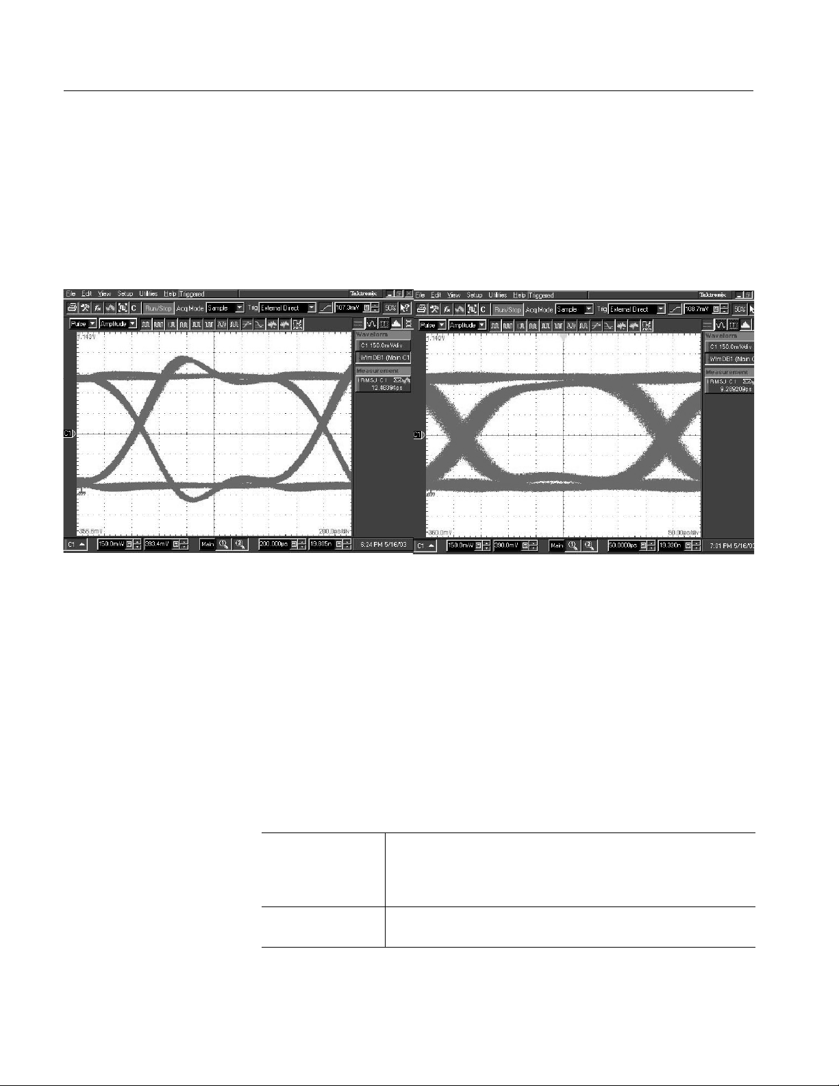
Performance Verification
2. Load the setup file (TOTJIT.dtg). Refer to Loading Files on page 1--13.
3. Push the RUN button of the data timing generator to light the RUN LED,
and then push the ALL OUTPUTS ON/OFF button to activate the output.
4. Verify that the oscilloscope displays the waveforms as shown in Figure 1--25
while adjusting the position and offset controls.
DTG5078
PG Mode
DTG5274
Figure 1--25: Total jitter waveform sample
5. Verify that the jitter rms values are within the following range.
H <18ps (DTG5078)
H <16ps (DTG5274)
6. Repeat the same measurements for other channels.
This test verifies that the PG Mode of the DTG5000 series mainframe is
functional.
Equipment
required
Prerequisites
One oscilloscope (TDS7104) (item 3)
Two 50 Ω SMA coaxial cables (item 6)
Two SMA (female)-BNC (male) adapters (item 9)
DTG5000 Series Data Timing Generator
The
prerequisites listed on page 1 --11.
must meet the
1--54
DTG5078 & DTG5274 Data Timing Generator Technical Reference

Performance Verification
1. Install the test hookup and preset the instrument controls:
a. Hook up the oscilloscope:
H Attach SMA (female)-BNC (male) adapters to the oscilloscope CH1
input and CH2 input connectors.
H Connect an SMA coaxial cable from t he CH1 connector of the
output module, which is inserted in the slot A of DTG5000 series
mainframe, to the SMA-BNC adapter (CH1 input) of oscilloscope.
H Connect an SMA coaxial cable from t he CH2 connector of the
output module, which is inserted in the slot A of DTG5000 series
mainframe, to the SMA-BNC adapter (CH2 input) of oscilloscope.
See Figure 1--26.
CH1 of output
module
CH2 of output
module
Figure 1--26: PG Mode tests
DTG5000 series
CH1 Input
+ SMA (female)-BNC (male) adapter
50 Ω SMA coaxial cables
b. Set the oscilloscope controls as follows:
Vertical .
CH1andCH2scale ........... 500mV/div
CH1 and CH2 input impedance . . . 50 Ω
Horizontal
Scale ...................... 5ns/div
Trigger
Source ..................... CH2
Slope ...................... Positive
Level ...................... 0.5V
Oscilloscope (TDS7104)
CH2 Input
+ SMA (female)-BNC
(male) adapter
DTG5078 & DTG5274 Data Timing Generator Technical Reference
1--55

Performance Verification
2. Load the setup file (PGMODE.dtg). Refer to Loading Files on page 1--13.
3. Push the RUN button of the data timing generator to light the RUN LED,
and then push the ALL OUTPUTS ON/OFF button to activate the output.
4. Verify that 100 MHz square waveform is displayed on the oscilloscope
screen.
5. Verify the PG mode functions:
a. Push the TIMI NG button at the front panel of DTG5000 series
mainframe to display the Timing Window.
b. Move the cursor to Frequency and change the frequency to 200 MHz.
c. Verify that the frequency readout of displayed waveform is 200 MHz on
the oscilloscope screen.
d. Return the Frequency to 100 MHz, and then set the DTG5000 series
mainframe slot A CH1 DELAY to 0.0020000 s.
e. Verify on the oscilloscope screen that the rising edge of CH1 is delayed
by approximately 2 ns compared to CH2 rising edge.
6. Verify the CH1 duty:
a. Change the slot A CH1 Duty to 30%.
b. Verify on the oscilloscope screen that CH1 Duty of displayed waveform
also indicates approximately 30%.
c. Change the CH1 Duty to 50% , and then change the slot A CH1
Polarity to Invert.
d. Verify on the oscilloscope screen that the displayed waveform is
inverted.
7. (DTGM10 and DTGM20 only):
a. Push the RUN button of DTG5000 series mainframe to light the RUN
LED.
b. Move cursor to Slew Rate with the TAB key.
c. Decrease the slew rate value by rotating the rotary encoder counterclock-
wise.
1--56
d. Verify the displayed waveform: Confirm that the rising edge becomes
slow on the oscilloscope screen.
DTG5078 & DTG5274 Data Timing Generator Technical Reference

Performance Verification
Master-Slave Operation
This test verifies that the Master-Slave operation of the DTG5000 series
mainframe is functional.
Equipment
required
Prerequisites
One oscilloscope (TDS7104) (item 3)
Two 50 Ω SMA coaxial cables (item 6)
Two 50 Ω BNC coaxial cables (item 7)
Two SMA (male)-BNC (female) adapters (item 8)
DTG5000 Series Data Timing Generator
The
prerequisites listed on page 1 --11.
must meet the
1. Install the test hookup and preset the instrument controls:
a. Hook up the oscilloscope:
H Use an SMA coaxial cable to connect CLK IN and CLK OUT1 of
the Maser/Slave Connection plate at the rear panel of DTG5000
series mainframe.
H Use a second SMA coaxial cable to connect CLK IN
OUT1
of the Maser/Slave Connection plate at the rear panel of
and
CLK
DTG5000 series mainframe.
H Attach an SMA (male)-BNC (female) adapter to the CLOCK OUT
at the rear panel of DTG5000 series mainframe.
H Connect a BNC coaxial cable from the CLOCK OUT to the CH1
input of oscilloscope through an SMA-BNC adapter.
H Attach an SMA (male)-BNC (female) adapter to the CH1 connector
of the output module, which is inserted in the slot A of DTG5000
series mainframe.
H Connect a BNC coaxial cable from the CH1 connector of output
module to the CH2 input of oscilloscope through an SMA-BNC
adapter. See Figure 1--27.
DTG5078 & DTG5274 Data Timing Generator Technical Reference
1--57

Performance Verification
DTG5000 series rear
CLOCK OUT
+ SMA (male)-BNC (female) adapter
DTG5000 series
CH1 output
+ SMA (male)-BNC (female) adapter
DTG5078 Master Slave connecter location
50 Ω BNC coaxial cable
CH1 Input
50 Ω BNC coaxial cable
Oscilloscope (TDS7104)
CH2 Input
DTG5274 Master Slave connecter location
Figure 1--27: Master-Slave operation tests
b. Set the oscilloscope controls as follows:
Vertical .
CH1andCH2scale ........... 500mV/div
CH1 and CH2 input impedance . . . 50 Ω
Horizontal
Scale ...................... 50ns/div
1--58
DTG5078 & DTG5274 Data Timing Generator Technical Reference

Performance Verification
Trigger
Source ..................... CH1
Slope ...................... Positive
Level ...................... +0.5V
2. Set the data timing generator controls and load the setup file:
a. Exit the DTG software.
NOTE. Move the cursor to the bottom left corner of the screen to get the Windows
Start menu. Or, press the CTRL and ESC keys simultaneously to open the
Windows Start menu.
b. From the Windows Start menu, select Programs, select Tektronix,
select DTG5000, and then select DTG5000 Configuration Utility.
See Figure 1--28.
Figure 1--28: DTG5000 Configuration Utility dialog
c. Confirm that Online is selected in the Mode box.
d. Select Master/Slave#1 from the System Configuration pull-down menu.
DTG5078 & DTG5274 Data Timing Generator Technical Reference
1--59

Performance Verification
e. Select IP Address at the Slaves Set by check box, and then enter 0.0.0.0
to the IP Address box.
f. Click OK to exit the window. The following dialog box appears and
asks you to restart the DTG software.
g. Click OK, and then restart the DTG software.
h. Load the setup file (MASTER.dtg). Refer to Loading Files on page
1--13.
3. Push the RUN button of the data timing generator to light the RUN LED,
and then push the ALL OUTPUTS ON/OFF button to activate the output.
4. Confirm that the oscilloscope displays the waveforms such as shown i n
Figure 1--29.
CH1
CH2
Figure 1--29: Master-Slave operation waveform sample
1--60
5. Disconnect the SMA cables from the CLK OUT1 and CLK OUT1
Reconnect the cables to CLK OUT2 and CLK OUT2
, respectively.
DTG5078 & DTG5274 Data Timing Generator Technical Reference
.

Performance Verification
6. Verify that the oscilloscope displays the same waveforms as step 4 on the
screen.
7. (DTG5078 only): Disconnect the SMA cables from the CLK OUT2 and
CLK OUT2
respectively. Verify that the oscilloscope displays the same waveforms as
step 4 on the screen.
8. Before proceeding with the next test item, do the following substeps.
a. Exit the DTG software.
NOTE. Mover cursor to the button left corner of the screen to get the Windows
Start menu. Or, press the CTRL + ESC keys simultaneously to open the Start
menu.
b. From the Windows Start menu, select Programs, select Tektronix,
select DTG5000, and then select DTG5000 Configuration Utility.
See Figure 1--28 on page 1--59.
. Reconnect the cables to CLK OUT3 and CLK OUT3,
c. Select Master from the System Configuration pull-down menu.
d. Click OK to exit the window. The dialog box appears and asks you to
restart the DTG software. Click OK, and then restart the DTG software.
DTG5078 & DTG5274 Data Timing Generator Technical Reference
1--61

Performance Verification
Output Module
The following procedures check those characteristics that relate to the output
modules that are checked under Output Module in Specifications. Refer to page
2--27.
NOTE. When you perform the DTG5000 series output module performance tests,
you can install the module to any slot of mainframe.
There are three types of output modules: DTGM10, DTGM20, and DTGM30.
The same performance test procedures are applied to these modules, however,
each module has different specifications.
Data Output DC Level
This test verifies the data output DC level accuracy of the DTG5000 series
output module.
Equipment
required
Prerequisites
One digital multi meter (item 2)
One 50 Ω BNC coaxial cable (item 7)
One SMA (male)-BNC (female) adapter (item 8)
One BNC (female)- dual banana plug (item 13)
One Feed-through 50 Ω termination (item 15)
DTG5000 Series Data Timing Generator
The
prerequisites listed on page 1 --11.
must meet the
1. Install the test hookup and preset the instrument controls:
a. Hook up the digital multi meter:
H Attach a BNC (female)-dual banana adapter to the digital multi
meter input connector, and then attach a 50 Ω termination to the
BNC-dual banana adapter.
H Attach an SMA (male)-BNC (female) adapter to the CH1 connector
of the output module, which is inserted in the slot A of DTG5000
series mainframe.
1--62
H Connect a BNC coaxial cable from the SMA-BNC adapter (CH1
output of output module) to the 50 Ω termination of digital multi
meter. See Figure 1--30.
DTG5078 & DTG5274 Data Timing Generator Technical Reference

CH1 output
+ SMA (male)-BNC (female) adapter
Figure 1--30: Data output DC level tests
b. Set the digital multi meter controls:
Mode .......................... DirectVoltage
Range ......................... Auto
DTG5000 series
50 Ω BNC coaxial cable
Performance Verification
DMM
Input connector
+ BNC-dual banana adapter
+BNC50Ω termination
2. If you want to perform the data output DC level tests for DTGM10 or
DTGM20, continue the following steps. If your output module is DTGM30,
jump to step 5.
3. Do the following substeps to perform the high/low level voltage measurements:
a. Load the setup file (OM_H.dtg). Refer to Loading Files on page 1--13.
b. Push the RUN button of the data timing generator to light the RUN
LED, and then push the ALL OUTPUTS ON/OFF button to activate
the output.
c. Push the LEVEL button to set the high level and corresponding low
level voltage for the CH1 output as shown in Table 1--4 (DTGM10) or
Table 1--6 (DTGM20).
d. Verify that the DMM readings are within the voltage limits.
e. Load the setup file (OM_L.dtg). Refer to Loading Files on page 1--13.
f. Push the LEVEL button to set the low level and corresponding high
level voltage for the CH1 output as shown in Table 1--5 (DTGM10) or
Table 1--7 (DTGM20).
g. Verify that the DMM readings are within the voltage limits.
DTG5078 & DTG5274 Data Timing Generator Technical Reference
1--63

Performance Verification
4. Change the connections and repeat the measurements:
a. Change the connection of BNC cable from the CH1 output to CH2,
CH3, and CH4 output.
b. Perform the same measurements as step 3 for every channel.
c. Verify that the high level and low level measurements are within the
specified voltage limits.
Table 1--4: DTGM10 High Level Voltage Accuracy
Setup value
High Level Voltage Low Level Voltage
-- 1 . 0 V -- 1 . 5 V -- 1.08 V to -- 0.92 V
0V -- 1 . 5 V -- 0.05 V to + 0.05 V
1V -- 1 . 5 V 0.92 V to 1.08 V
2V -- 1 . 5 V 1.89 V to 2.11 V
High Level Output Voltage Limits
Table 1--5: DTGM10 Low Level Voltage Accuracy
Setup value
Low Level Voltage High Level Voltage
-- 1 . 0 V 2.0 V -- 1.08 V to -- 0.92 V
0V 2.0 V -- 0.05 V to + 0.05 V
1V 2.0 V 0.92 V to 1.08 V
1.75 V 2.0 V 1.6475 V to 1.8525 V
Low Level Output Voltage Limits
Table 1--6: DTGM20 High Level Voltage Accuracy
1--64
Setup value
High Level Voltage Low Level Voltage
-- 0 . 9 V -- 1 . 0 V -- 0.977 V to -- 0.823 V
0V -- 1 . 0 V -- 0.05 V to + 0.05 V
1.0 V -- 1 . 0 V 0.92 V to 1.08 V
2.0 V -- 1 . 0 V 1.89 V to 2.11 V
High Level Output Voltage Limits
DTG5078 & DTG5274 Data Timing Generator Technical Reference

Table 1--7: DTGM20 Low Level Voltage Accuracy
Setup value
Performance Verification
Low Level Voltage High Level Voltage
-- 1 . 0 V 2.5 V -- 1.08 V to -- 0.92 V
0V 2.5 V -- 0.05 V to + 0.05 V
1.0 V 2.5 V 0.92 V to 1.08 V
2.0 V 2.5 V 1.89 V to 2.11 V
Low Level Output Voltage Limits
5. Do the following substeps to perform the high/low level voltage measurements for the DTGM30:
a. Load the setup file (OM_H.dtg). Refer to Loading Files on page 1--13.
b. Push the RUN button of the data timing generator to light the RUN
LED, and then push the ALL OUTPUTS ON/OFF button to activate
the output.
c. Push the LEVEL button to set the high level and corresponding low
level voltage for the CH1 output as shown in Table 1--8. Verify that the
DMM reading is within the voltage limits.
d. Load the setup file (OM_L.dtg). Refer to Loading Files on page 1--13.
e. Push the LEVEL button to set the low level and corresponding high
level voltage for the CH1 output as shown in Table 1--9. Verify that the
DMM reading is within the voltage limits.
6. Change the connections and repeat the measurements:
a. Change the connection of BNC cable from the CH1 output to CH2,
,andCH2output.
CH1
b. Perform the same measurements as step 5 for every channel.
c. Verify that the high level and low level measurements are within the
specified voltage limits.
NOTE. When you perform the voltage measurements for CH1
setup file OM_L.dtg for high level measurements and OM_H.dtg for low level
measurements.
DTG5078 & DTG5274 Data Timing Generator Technical Reference
and CH2, load the
1--65

Performance Verification
Table 1--8: DTGM30 High Level Voltage Accuracy
Setup value
High Level Voltage Low Level Voltage
-- 0.97 V -- 1 . 0 V -- 1.0491 V to -- 0.8909 V
0.5 V -- 0.75 V 0.435 V to 0.565 V
2.0 V 1.50 V 1.89 V to 2.11 V
2.47 V 2.44 V 2.3459 V to 2.5941 V
High Level Output Voltage Limits
Table 1--9: DTGM30 Low Level Voltage Accuracy
Setup value
Low Level Voltage High Level Voltage
-- 1 . 0 V 0.25 V -- 1.08 V to -- 0.92 V
0.5 V 1.50 V 0.435 V to + 0.565 V
2.0 V 2.25 V 1.89 V to 2.11 V
2.44 V 2.47 V 2.3168 V to 2.5632 V
Low Level Output Voltage Limits
1--66
DTG5078 & DTG5274 Data Timing Generator Technical Reference

Performance Verification
Data Format
This test verifies that the data format of the DTG5000 series mainframe is
functional.
Equipment
required
Prerequisites
One oscilloscope (TDS7104) (item 3)
Two 50 Ω SMA coaxial cables (item 6)
Two SMA (female)-BNC (male) adapters (item 9)
DTG5000 Series Data Timing Generator
The
prerequisites listed on page 1 --11.
must meet the
1. Install the test hookup and preset the instrument controls:
a. Hook up the oscilloscope:
H Attach SMA (female)-BNC (male) adapters to the oscilloscope CH1
and CH2 input connectors.
H Connect an SMA coaxial cable from t he CH1 connector of the
output module, which is inserted in the slot A of DTG5000 series
mainframe, to the SMA-BNC adapter (CH1 input) of oscilloscope.
H Connect an SMA coaxial cable from t he CH2 connector of the
output module, which is inserted in the slot A of DTG5000 series
mainframe, to the SMA-BNC adapter (CH2 input) of oscilloscope.
See Figure 1--31.
DTG5000 series
CH1 of output
module
CH2 of output module
CH1 Input
+ SMA (female)-BNC (male) adapter
50 Ω SMA coaxial cables
Figure 1--31: Data format tests
DTG5078 & DTG5274 Data Timing Generator Technical Reference
Oscilloscope (TDS7104)
CH2 Input
+ SMA (female)-BNC
(male) adapter
1--67

Performance Verification
b. Set the oscilloscope controls as follows:
Vertical .
CH1andCH2scale ........... 500mV/div
CH1 and CH2 input impedance . . . 50 Ω
Horizontal
Scale ...................... 50ns/div
Trigger
Source ..................... CH2
Slope ...................... Positive
Level ...................... 0.5V
2. Load the setup file (FORMAT.dtg). Refer to Loading Files on page 1--13.
3. Do the following substeps to verify the data format:
a. Push the RUN button of the data timing generator to light the RUN
LED, and then push the ALL OUTPUTS ON/OFF button to activate
the output.
b. Verify that the oscilloscope displays pulse pattern such as shown in
Figure 1--32.
Figure 1--32: Pulse pattern example
c. Push the TIMING button at the front panel of DTG5000 series
mainframe to display the Timing Window.
1--68
DTG5078 & DTG5274 Data Timing Generator Technical Reference

Performance Verification
d. Change CH1 Format of slot A from NRZ to RZ. Verify that the
displayed waveform is changed from Figure 1--32 to Figure 1--33.
Figure 1--33: RZ waveform example
e. Change CH1 Format of slot A from RZ to R1. Verify that the displayed
waveform is changed from Figure 1--33 to Figure 1--34.
Figure 1--34: R1 waveform example
DTG5078 & DTG5274 Data Timing Generator Technical Reference
1--69

Performance Verification
1--70
DTG5078 & DTG5274 Data Timing Generator Technical Reference

Specifications
This section contains the DTG5000 Series Data Timing Generator specifications.
All specifications are guaranteed unless labeled “typical”. Typical specifications
are provided for your convenience but are not guaranteed.
Specifications that are check marked with the
indirectly) in the Performance Verification chapter of this manual.
Performance Conditions
The performance limits in this specification are valid with these conditions:
H The instrument must have been calibrated/adjusted at an ambient tempera-
ture between +20
H The instrument must be in an environment with temperature, altitude,
humidity, and vibration within the operating limits described in these
specifications.
H The instrument must have had a warm-up period of at least 20 minutes.
H The instrument must be operating at an ambient temperature between +10
and +40
Product and Feature Description
The DTG5000 Series Data Timing Generator is a high speed/multichannel signal
generator which creates a wide range of digital timing signals. The products are
designed to generate a data pattern for standard and nonstandard pulses necessary
for functional tests or characterization of legacy devices (TTL, CMOS, ECL) as
well as the latest devices (PECL, LVDS, GTL, CML).
symbol are checked directly (or
n
Cand+30_C.
_
C
_
C.
_
Table 2--1 shows the data timing generator family.
Table 2--1: DTG5000 Series Data Timing Generators
DTG5078 DTG5274
Maximum clock
frequency/ Maximum data rate
Number of slot 8 (A, B, C, D, E, F, G, and H) 4 (A, B, C, and D)
Pattern length 240 to 8,000,000 words/channel 960 to 32,000,000 words/channel
Block size
granularity
DTG5078 & DTG5274 Data Timing Generator Technical Reference
750 MHz/750 Mb/s 2.7 GHz/2.7 Gb/s
1 1 to 4 (depends on Vector Rate)
2--1

Specifications
,
,
Table 2--1: DTG5000 Series Data Timing Generator s (cont.)
DTG5274DTG5078
Sequence steps 1 to 8,000 steps 1 to 8,000 steps
Sequence repeat
counter
Data Generator
Mode
Data format Slots A to D NRZ, RZ, and R1 Slots A to D NRZ, RZ, and R1
Data rate NRZ 50 kb/s to 750 Mb/s NRZ 50 kb/s to 2.7 Gb/s
Channel addition SlotsA,B,C,andD SlotsA,B,C,andD
Jitter generation Channel 1 of slot A Channel 1 of slot A
Lead delay
resolution
Trail delay
resolution
Pulse width
resolution
Pulse Generator
Mode
Clock frequency 50 kHz to 375 MHz 50kHzto1.35GHz
Output Module
Number of
channel
Amplitude (50 Ω) 3.5 V
Amplitude
(1 MΩ)
Rise time/fall
time at 1 Vp-p
into 50 Ω
(20% to 80%)
Master-Slave Up to three (one Master, two Slaves) Up to two (one Master, one Slave)
1 to 65,536 or Infinite 1 to 65,536 or Infinite
SlotsA,B,C,D,E,F,G,andH SlotsA,B,C,andD
Slots E to H NRZ
RZ and R1 50 kb/s to 375 Mb/s RZ and R1 50 kb/s to 1.35 Gb/s
1ps 0.2 ps
5ps 5ps
5ps(slotsA,B,C,andD) 5ps(slotsA,B,C,andD)
SlotsA,B,C,andD SlotsA,B,C,andD
DTGM10 DTGM20 DTGM30 DTGM10 DTGM20 DTGM30
4 4 2 2of4
(CH1, CH2)
p-p
10 V
p-p
<540 ps
(variable)
1
3.5 V
p-p
7V
p-p
<340 ps
(variable)
1.25 V
2.5 V
p-p
p-p
3.5 V
10 V
<110 ps <540 ps
(variable)
p-p
p-p
1
2of4
(CH1, CH2)
3.5 V
p-p
7V
p-p
<340 ps
(variable)
2
1.25 V
p-p
2.5 V
p-p
<110 ps
1
This value is limited by the maximum output current (+/-- 40 mA, maximum).
Additional product information is located within the User and Service manuals.
See Related Manuals and Online Documents on page vii in the Preface.
2--2
DTG5078 & DTG5274 Data Timing Generator Technical Reference

Electrical Specification
Mainframe
Table 2--2: Operation mode
Characteristics Description
Data Generator Mode
(DG Mode)
Pulse Generator Mode
(PG Mode)
Operates as a data generator. The output data are created through built--in pattern editor or
imported files created by external simulation software tools. The output timing is defined by
sample clock rate.
Note: Jump is not available if Long Delay is set to On.
Operates as a pulse generator. The output timing is defined by signal output frequency.
Specifications
-- Timing control: Delay, Slew rate, Width
-- Level control: High/Low or Amplitude/Offset
-- Supports flexible block branching sequence function.
-- Timing control: Pulse width, Delay, Duty, Slew rate
-- Level control: High/Low or Amplitude/Offset
Table 2--3: Sequencer
Characteristics Description
Pattern Length
DTG5078
Hardware Sequence 240 to 8,000,000 words
Software Sequence 1 to 8,000,000 words
DTG5274
Hardware Sequence 960 to 32,000,000 words
Software Sequence 1 to 32,000,000 words
Pattern Length Granularity
DTG5078
Hardware Sequence 1word
Software Sequence 1word
DTG5274
Hardware Sequence Depends on vector rate. Refer to Table 2 --23 and Table 2--24.
Software Sequence 1word
Sequence Length 1 to 8000 steps
Maximum Blocks 8000
Maximum sub-sequences 50
Sub-sequence Length 1 to 256 steps
Sequence Repeat Counter 1 to 65,536 or Infinite, All channels operate the same sequence.
DTG5078 & DTG5274 Data Timing Generator Technical Reference
2--3

Specifications
Table 2--4: Clock Generator
Characteristics Description PV reference page
Clock Frequency
DTG5078 50 kHz to 750 MHz
DTG5274 50kHzto3.35GHz
Resolution 8 digits
Internal clock
n Accuracy
2
The internal reference oscillator is used.
2
within 1 ppm Page 1--18
Table 2--5: Internal Trigger Generator
Characteristics Description
Internal trigger rate
Range 1.0 s to 10.0 s
Resolution 3 digits, minimum 0.1 s
3
The internal reference oscillator is used.
3
Table 2--6: DC Output
Characteristics Description PV reference page
Connector 2.54 mm 2 x 8 pin header (female), front right side
Number of Channel 8
Source Resistance approximately 1 Ω
Level
Voltage Range --3.0 V to 5.0 V
Control Independent
Resolution 10 mV
nDC Accuracy
Maximum Output Current
Pin Assignment Refer to Figure 2--1.
(3% of the set value)50 mV Page 1--42
30 mA
2--4
DTG5078 & DTG5274 Data Timing Generator Technical Reference

CH0 GND
CH1 GND
CH2 GND
CH3 GND
CH4 GND
CH5 GND
CH6 GND
CH7 GND
Figure 2--1: DC Output channel assignment
Specifications
Table 2--7: Clock Out
Characteristics Description PV reference page
Output connector SMA rear
Output Signal Type Complementary
Frequency
DTG5078 50 kHz to 750 MHz
DTG5274 50kHzto3.35GHz
Impedance 50 Ω
Output Voltage Level
Range
High Level (VOH)
Low Level (VOL)
Output Voltage Amplitude
Range 30 mV
Resolution 10 mV
Output Voltage Frequency Response
4
5
6
7
-- 1.00 V to 2.47 V into 50 Ω to GND
-- 1.94 V to 7.00 V into 1 MΩ to GND
-- 2.00 V to 2.44 V into 50 Ω to GND
-- 2.00 V to 6.94 V into 1 MΩ to GND
to 1.25V
p-p
60 mV
10 dB of value shown in the curve of Figure 2--2.
p-p
to 2.5V
into 50 Ω to GND
p-p
into 1 MΩ to GND
p-p
DTG5078 & DTG5274 Data Timing Generator Technical Reference
2--5

Specifications
g
g
Table 2--7: Clock Out (cont.)
Characteristics PV reference pageDescription
Output Voltage Offset
Resolution 40 mV
Range Depends on the limit of VOH and VOL set by the user.
Refer to Output Voltage Level.
Offset = (VOH + VOL) /2
Maximum Output Current
nRise /Fall Time (20% to 80%), typical
DTG5078
at 100 mV
amplitude,
p-p
0 V offset
at 1.00 V
amplitude,
p-p
0 V offset
DTG5274
at 100 mV
amplitude,
p-p
0 V offset
at 1.00 V
amplitude,
p-p
0 V offset
nAberration, typical
Positive Overshoot
Negative Overshoot
nRandom Jitter, typical
DTG5078
DTG5274
4
When the amplitude and offset are set up, the VoH and VoL are automatically set up in DTG5000 series.
There is no menu to set the VoH or VoL directly. Refer to Figure 2--11 on page 2--31.
5
High level (VoH) should fulfill the following formulas simultaneously.
R
=TermR,Vtt=TermV
L
VOH
VOH
VOH
VOH
VOH
±
7.00
±
(7.00 x RL + 50 x Vtt) / (RL + 50)
±
RL / 50 x (2.5 -- 0.06 x RL / (RL + 50)) + Vtt
²
(--2.00 x RL + 50 x Vtt) / (RL + 50)
²
Vtt -- RL / 50
80 mA
<85 ps into 50 Ω to GND
<100 ps into 50 Ω to GND
<70 ps into 50 Ω to GND
<80 ps into 50 Ω to GND
<10 % at 1V
<10 % at 1V
into 50 Ω Page 1--20
p-p
into 50 Ω
p-p
Measured by RMS jitter in Measurement function of CSA8000 + 80E03.
<2 ps rms, at 750 Mb/s, amplitude = 0.8 V
<2 ps rms, at 2.7 Gb/s, amplitude = 0.8 V
p-p
p-p
Page 1--20
Page 1--20
Page 1--47
6
Low level (VoL) should fulfill the following formulas simultaneously.
=TermR,Vtt=TermV
R
L
²
VOL
VOL
VOL
--2.00
²
(50 x Vtt -- 4.5 x RL) / (RL + 50)
²
Vtt -- RL (0.02 + 2.5 / (RL + 50))
VOL < ((2.5 -- 0.06) x RL / 50) + Vtt
2--6
DTG5078 & DTG5274 Data Timing Generator Technical Reference

7
Amplitude should fulfill the following formulas simultaneously. Amplitude = VOH -- VOL
=TermR,Vtt=TermV
R
L
VOH -- VOL > 2 x (Vtt -- RL/50 -- Offset)
VOH -- VOL > 2 x ((RL x (--2) + 50 x Vtt) / (RL + 50) -- Offset)
VOH -- VOL < 2 x ((2.5 x RL -- 50 x Offset + 50 x Vtt) / (2 x RL + 50))
VOH -- VOL < 2 x ((7 x RL -- 50 x Vtt) / (RL + 50) -- Offset)
(1) at 0.5 Vp--p
Specifications
(2) at 1.0 Vp--p
Figure 2--2: Frequency response of clock output
Table 2--8: External Clock In
Characteristics Description
Connector SMA rear
Impedance 50 Ω, AC coupled
Required Input Voltage Swing 400 mV
Required Duty Cycle 50 5%
p-p
to 2 V
into 50 Ω
p-p
DTG5078 & DTG5274 Data Timing Generator Technical Reference
2--7

Specifications
Table 2--8: External Clock In (cont.)
Characteristics Description
Frequency Range Slew rate should be more than 10 mV/ns.
DTG5078 1 MHz to 750 MHz
DTG5274 1 MHz to 2.7 GHz
Table 2--9: 10 MHz Reference In
Characteristics Description PV reference page
Connector BNC rear
Impedance 50 Ω, AC coupled,
Required Input Voltage Swing 200 mV
nFrequency Range
10 MHz0.1 MHz Page 1--25
p-p
to 3 V
p-p
Table 2--10: 10 MHz Reference Out
Characteristics Description PV reference page
Connector BNC rear
Impedance 50 Ω, AC coupled
nAmplitude, typical
1.2 V
2.4 V
into 50 Ω to GND
p-p
into 1 MΩ to GND
p-p
Page 1--26
Table 2--11: Phase Lock In
Characteristics Description PV reference page
Connector BNC rear
Impedance 50 Ω, AC coupled
Required Input Voltage Swing 200 mV
nFrequency Range
Multiplier Rate
8
1 MHz to 200 MHz Page 1--28
Long Delay, Off
NRZ x N, The maximum value of N is limited by the maximum data rate.
RZ and R1 x N/2, The maximum value of N is limited by the maximum data rate.
Long Delay, On x N / (vector rate)
8
N is an arbitrary integer.
p-p
to 3 V
p-p
2--8
DTG5078 & DTG5274 Data Timing Generator Technical Reference

Table 2--12: Skew Cal In
Characteristics Description
Connector
9
SMA front
Input Signal Type Single end
Level ECLinto50Ω to --2 V
9
This input is used only in calibrating a skew between channels. Refer to the reference manual for details.
Table 2--13: Trigger In
Characteristics Description
Connector BNC front
Impedance 1kΩ or 50 Ω
Slope Positive or Negative
Input Voltage Range -- 1 0 V t o 1 0 V, 1 k Ω selected
--5Vto5V,50Ω selected
Threshold
Level -- 5.0 V to 5.0 V
Resolution 0.1 V
Required Minimum Input Swing 1.0 V
Required Minimum Pulse Width (Pw1) 20 ns, refer to Figure 2--3.
Maximum Delay Time to Data Out (Td1) Refer to Figure 2--3.
DTG5078 47 H/W Clocks + 5 VCO (Ext) Clocks + 50 ns
DTG5274 201 H/W Clocks + 5 VCO (Ext) Clocks + 50 ns
Trigger Holdoff Time (Td 3) Refer to Figure 2--3.
DTG5078 29 H/W Clocks + 500 ns
DTG5274 115 H/W Clocks + 500 ns
0.5 V
,1kΩ selected
p-p
,50Ω selected
p-p
Specifications
DTG5078 & DTG5274 Data Timing Generator Technical Reference
2--9

Specifications
g
Table 2--14: Sync Out
Characteristics Description
10
Connector SMA front
Output Signal Type Single end
nLevel, typical
CML (Current Mode Logic)
VOH 0Vinto50Ω to GND Page 1--15
VOL --0.4 V into 50 Ω to GND
Pulse Width (Pw 2) Refer to Figure 2--3.
DTG5078 4 Clocks
DTG5274 4 Clocks
Delay Time to Data Out (Td2), typical -- 4.5 ns, refer to Figure 2--3.
Rise/Fall Time (20 to 80%)
10
DG Mode: A positive pulse is generated at the beginning of each block.
<140 ps
PG Mode: A positive pulse is generated on each trigger if the Run Mode is set to Burst.
Sync Out is not available if the Run Mode is set to Continuous.
Table 2--15: Sync Clock In
Characteristics Description
Connector SMA rear
Output Signal Type Complementary
11
This signal is used for only Master Slave performance test with another DTG5000 series instrument.
Refer to the reference manual for details. The cable connection in Master-Slave operation in units is
shown in Figure 2--4 and Figure 2--5.
11
PV reference page
Table 2--16: Sync Clock Out 1, Out 2 and Out 3
Characteristics Description
Connector SMA rear
Output Signal Type Complementary
12
This signal is used for only Master Slave performance test with another DTG5000 series instrument.
Refer to the reference manual for details. Sync Clock Out 3 is equipped only with DTG5078.
The cable connection in Master-Slave operation in units is shown in Figure 2--4 and Figure 2--5.
2--10
12
DTG5078 & DTG5274 Data Timing Generator Technical Reference

Table 2--17: Sync Jump In
Specifications
Characteristics Description
13
Connector BNC rear
13
This signal is used for only Master Slave performance test with another DTG5000 series instrument.
Refer to the reference manual for details. The cable connection in Master-Slave operation in units is
shown in Figure 2--4 and Figure 2--5.
Table 2--18: Sync Jump Out 1, Out 2 and Out 3
Characteristics Description
Connector BNC rear
14
This signal is used for only Master Slave performance test with another DTG5000 series instrument.
Refer to the reference manual for details. Sync Jump Out 3 is equipped only with DTG5078.
The cable connection in Master-Slave operation in units is shown in Figure 2--4 and Figure 2--5.
14
DTG5078 & DTG5274 Data Timing Generator Technical Reference
2--11

Specifications
Trigger Trigger Start
:«:É:À::::É
:: ::w: «:É:À::::É:w:: ¯
Ext Trigger in
::: :::w::Ì :
Clock Out
Data Out
:::::w::Ì:
:::¯::w::Ì:Ë:w::Ì:acc3acb
Sync Out
:«:É:À:: : :É:w: : ::É:
::::::::::::::: ::::::::::::::8:::::::::::::8::::::::::::8:::::::::8::::::8::::8:::8::8
:§: ::8
Pw1
:8
:«:»:
Td1
:«:»:
Td2
:§: ::9
Pw2
Stop Trigger Start
:«:É:À: : : :É:w: : : :É:::: :
:: :
Trigger Holdoff
:«:É:À::::É:w:: ::»:w:::
:«:»:
Td3
Event
Ext Event In
Data Out
Sync Jump
Out
Block_1 Block_2 Block_3
:«:»:
:§: ::b
Td6
Pw4
Pw3
:§: ::a
: : ::¯::w::Å:Ç:Ì:Ë:w::¯: :Ì:ac73acc3ac
Event Input
: :À:¯:À::Ì::w:§ :Ì::::w: :À:»::¿
Minimum Pulse Width
Delay Time to Data Out
::::::w:«:À:::w:: :w:::::w::Ì:
:«:»:
Td4
Event Holdoff
:: ::¯::w:: ::»:w:::
:«:»:
Td5
::: :::¶:
Figure 2--3: Signal timing
2--12
DTG5078 & DTG5274 Data Timing Generator Technical Reference

Master Unit
Out1
Sync Clock
Sync JumpInOut1
Out1
Out2
Out2
Out3
Out3
Out2
Out3
Specifications
DTG5078DTG5078
Slave Unit
In
In
In
In
Out1
Out1
Out2
Out2
Out3
Out3
In
Out1
Out2
Out3
Sync Clock
Sync Jump
Local
Ethernet
Network
BNC Cable
SMACable
LAN Cable
LAN
(012--0076--00)
(174--1427--00)
LAN
In
In
Out1
Out1
Out2
Out2
Out3
Out3
In
Out1
Out2
Out3
LAN
DTG5078
Slave Unit
Sync Clock
Sync Jump
Figure 2--4: DTG5078 Master-Slave connection
DTG5078 & DTG5274 Data Timing Generator Technical Reference
2--13

Specifications
DTG5274 DTG5274
Master Unit
Sync Clock
In
In
Out1
Out1
Out2
Out2
In
In
Out1
Out1
Out2
Out2
Slave Unit
Sync Clock
Sync Jump
Out1
Out2
LAN
Local
Ethernet
Network
In
BNC Cable
SMA Cabl e
LAN Cable
Figure 2--5: DTG5274 Master-Slave connection
In
Out1
Out2
LAN
(012--0076--00)
(174--1427--00)
Sync Jump
Table 2--19: Event In
Characteristics Description
Connector BNC front
Impedance 1kΩ or 50 Ω
Polarity Normal or Invert
Input Voltage Range -- 1 0 V t o 1 0 V, 1 k Ω selected
--5Vto5V,50Ω selected
2--14
DTG5078 & DTG5274 Data Timing Generator Technical Reference

Table 2--19: Event In (cont.)
Characteristics Description
Threshold
Level -- 5.0 V to 5.0 V
Resolution 0.1 V
Required Minimum Input Swing 1.0 V
Required Minimum Pulse Width
DTG5078 32 H/W Clocks + 10 ns
DTG5274 128 H/W Clocks + 10 ns
Maximum Delay Time to Data Output
(Td4)
DTG5078 402 H/W Clocks
DTG5274 1621 H/W Clocks
Event Holdoff Time (Td5) at Asynchronous Jump Mode, refer to Figure 2--3.
DTG5078 320 H/W Clocks
DTG5274 1280 H/W Clocks
,1kΩ selected
p-p
0.5 V
,50Ω selected
p-p
at Asynchronous Jump Mode, refer to Figure 2--3.
Specifications
Table 2--20: CPU module and peripheral devices
Characteristics Description
CPU Celeron 566 MHz
Core Chip Intel 815E (815GMCH + ICH12)
DRAM 128 MB SDRAM
Storage
Hard Disk
USB USB 1.1
Ethernet 10BASE--T, 100BASE--TX, rear
Video Output
Connector 15 pin Dsub, rear
Format VGA (640 X 480), SVGA (800 X 600), XGA (1024 X 768),
GPIB 24 pin, IEEE488.2, rear
Drive Floppy disk 1.44 MB, front
Keyboard Connector PS/2 type connector (6-pin mini-DIN), rear
Mouse Connector PS/2 type connector (6-pin mini-DIN), rear
≥20 GB, User usable area is about 90 %
Series A 2ch Receptacle, rear
Series A 1ch Receptacle, front right side
SXGA (1280 X 1024), UXGA (1600 X 1200)
CD-ROM, rear
DTG5078 & DTG5274 Data Timing Generator Technical Reference
2--15

Specifications
Table 2--20: CPU module and peripheral devices (cont.)
Characteristics Description
Serial Port RS232C, 9 pin Dsub, rear
Physical Specifications Comply with IEEE1101.10
233.4 mm ( W) x 160 mm (D) x 40 mm (H)
Real Time Clock
Lifetime >5 years
Type Coin type lithium battery, CR2032 (Li 3 V 220 mAh)
Table 2--21: Display
Characteristics Description
Display Area Horizontal: 170.4 mm (6.71 in)
Vertical: 127.8 mm (5.03 in)
Resolution
800 (H) × 600 (V) pixels (SVGA)
Output Pattern
Table 2--22: DG Mode
Characteristics Description PV reference page
Data Format
Slot A to D NRZ, RZ, R1
Slot E to H NRZ
Data Rate
DTG5078
NRZ only 50 kb/s to 750 Mb/s
with RZ/R1 50 kb/s to 375 Mb/s
DTG5274
NRZ only 50 kb/s to 2.7 Gb/s
with RZ/R1 50 kb/s to 1.35 Gb/s
Data Rate Resolution
Internal Clock 8 digits
External Clock 4 digits
External Phase Lock In 4 digits
Clock Range Refer to Table 2--23 and Table 2-- 24.
2--16
DTG5078 & DTG5274 Data Timing Generator Technical Reference

Table 2--22: DG Mode (cont.)
g
Characteristics PV reference pageDescription
Channel Addition Slot E, F, G and H are not available in DTG5078.
Refer to Figure 2--6 on page 2-- 21.
Slot A, B, C and D.
Function AND or XOR.
Delay Offset
Range Refer to Table 2--25.
Resolution
DTG5078 1ps
DTG5274 0.2 ps
Lead Delay Refer to Figure 2--7 for definition and Figure 2--8 for maximum lead delay.
Range Refer to Table 2--26.
Resolution
DTG5078 1ps
DTG5274 0.2 ps
nAccuracy
DTG5078
DTG5274
Trail Delay Refer to Figure 2--7 for definition, available in RZ/R1.
Slot A, B, C and D.
Range Refer to Table 2--27.
Resolution 5ps
nAccuracy
Duty Cycle Refer to Figure 2--7 for definition, available in RZ/R1.
Slot A, B, C and D.
Range (Trail Delay -- Lead Delay) / Period x 100
Resolution 0.1%
Pulse Width Refer to Figure 2--7 for definition, available in RZ/R1.
Slot A, B, C and D.
Range Duty x Period / 100 or Trail Delay -- Lead Delay
Resolution 5ps
The timing reference is the lead edge which lead delay of each channel set to 0 ns.
Skew calibration includes temperature calibration.
100 ps, after skew calibration at + 20_Cto+30_C ambient
temperature. (Slot A, B, C, D)
150 ps, after skew calibration at + 20_Cto+30_C ambient
temperature. (Slot E, F, G, H)
100 ps, after skew calibration at + 20_Cto+30_C ambient
temperature.
100 ps, after skew calibration at + 20_Cto+30_C ambient
temperature.
The timing reference is the lead edge which lead delay of each channel set to 0 ns.
Skew calibration includes temperature calibration.
Page 1--44
Page 1--44
Specifications
DTG5078 & DTG5274 Data Timing Generator Technical Reference
2--17

Specifications
g
g
g
Table 2--22: DG Mode (cont.)
Characteristics PV reference pageDescription
Phase Phase = Lead Delay / Period x 100 (%)
Resolution 0.1%
Differential Timing Offset
Range --1.0nsto1.0ns
Resolution
DTG5078 1ps
DTG5274 0.2 ps
Skew Calibration Only the skew between channels of same type output module is calibrated.
Range 500 ps
nAccuracy
DTG5078 100 ps, after skew calibration (Slot A, B, C, D)
DTG5274 100 ps, after skew calibration
nRandom Jitter
DTG5078 (using DTGM20)
DTG5274 (using DTGM30)
nTotal Jitter
DTG5078 (using DTGM20)
DTG5274 (using DTGM30)
Cross Point
16
Slot A, B, C, and D
Range 30% to 70%
Resolution 2%
15
200 ps, after skew calibration (Slot E, F, H, G)
Page 1--44
Measured with clock pattern (01010...).
Measured by Histogram function of CSA8000 + 80E03.
<4 ps rms, at 750 Mb/s, delay = 0.0 ns, amplitude = 0.8 V
format = NRZ, slew rate = 2.25 V/ns, jitter mode = off
p-p
, data
Page 1--50
<3 ps rms, at 2.7Gb/s, delay = 0.0 ns, amplitude = 0.8 Vp-p, data
format = NRZ, jitter mode = off
Measured with PRBS2^15-1 pattern.
Measured by RMS Jitter and Pk-Pk Jitter in Measurement function of CSA8000 + 80E03.
<18 ps rms, (<85 ps
amplitude = 0.8 V, Data Format = NRZ, and Jitter mode off
<16 ps rms, (<60 ps
, typical), at 750 Mb/s, delay = 0.0 ns,
p-p
, typical), at 2.7 Gb/s, delay = 0.0 ns,
p-p
Page 1--53
amplitude = 0.8 V, Data Format = NRZ, and Jitter mode off
2--18
DTG5078 & DTG5274 Data Timing Generator Technical Reference
 Loading...