

Page 1

Page 2

Tektronix,
Inc.
p.0.
Box
500
Beaverton,
Oregon
97077
COMMlTED
EXCELLENCE
INSTRUCTION
MANUAL
Serial
Number
070-2692-
00
First
Printing
MAR
1979
Page 3

WARRANTY
his
Tektronix product is
1
~d
against
defect
rials
and
orkmanship, under normal
use,
for
a
period
of
one
year
rrom
date
f
initial shipment.
Tektronix
will repair
or
replace, at its
option,
bose
products determined to
be
defective within the warranty
eriod and returned, freight prepaid,
to
a
Tektronix Service Center.
here
is
no
implied warra itness
of
purpoa
art
numl
ive
mate
nty
for
f
i
for
ierl
lease
direct all
I
vice
or
replacerr
earest Tektronix
aerrlce
lvertrer
or
Field
Office;
include
the
rypr
or
Jer
of
th
requests
..--..I--
be.
lent
par'
vright
@
tents
oft
.
.
ct
and
it s serial
number.
nix, Inc.
lay
not
b
-.
ts
to
the
-I
--
his publication
rr
e
reprad
vllJ
,,, ,,,
without the
permission
of
Tektronix,
Inc.
Prod
cove
lucts
of
red
by
Tektro
U.S.
an
nix,
Inc
d
foreis
.
and
its
subsidiaries
are
In
patents
and/or
pending
patents.
TEKTRONIX
E-MOBILE,
and
@
are
registered
traaemar~s
or
r
edronix,
1
Printed
in
U.S.A.
privileges are reservt
nc.
3nd
pril
Page 4

TABLE
OF
CONTENTS
Page
................................................
LIST
OF
ILLUSTRATIONS
iv
.......................................................
LISTOFTABLES
V
...........................................
OPERdTORS
SAFETY SUMMARY
~ii
............................................
SERVICING
SAFETY
SUMMARY ix
SECTION
1
SPECIFICATIOM
...........................................
Introduction 1-1
..................................
Performance Conditions 1-1
........................
Electrical Characteristics (Front Panel) 1-1
........................................
Dc
Voltmeter 1-1
........................................
Ac
Voltmeter
1-2
..........................................
Ohmmeter
1-3
........................................
Dc
Ammeter 1-3
........................................
Ac
Ammeter
1-4
......................
Electrical Characteristics
(Rear
Interface)
1-4
Dc
Voltmeter
........................................
1-4
........................................
Ac
Voltmeter 1-5
..........................................
Ohmmeter
1-6
.........................................
Miscellaneous 1-7
..............................
Environmental Characteristics
1-7
........................................
DM
505 Only 1-7
.....................................
TM
500
Systems
1-8
..................................
Physical Characteristics 1-9
SECTION
2
OPERATING INSTRUCTIONS
...................................
l nstallation l nstructions 2-1
.................................
Controls
and
Connectors
2-2
.................................
Operators Familiarization
2-2
...........................
General Operating Information
2-2
....................................
l
nput
Connections
2-4
...................................
Si ne-wave Response
2-4
...............................
Dc
Voltage Measurements 2-4
..............................
Dc
Current Measurements
2-4
.....................
Ac
Voltage
and
Current Measurements
2-4
Resistance Measurements
...............................
2-4
Packaging Information
...................................
2-5
Page 5

TABLE
OF
CONTENTS
(cont)
Page
SECTION
6
OPTIONS ..............................................
61
SECTION
7
REPLACEABLE ELECTRICAL
PARTS
SECTION
8
DIAGRAMS
AND
CIRCUIT
BOARD
ILLUSTRATIONS
Simplified
Block
Diagram
Rear
Interface
Connections
ND
Block
Diagram
Adjustment
Locations
Troubleshooling
Flow
Charts
Parts
Locations
Component
Reference
Charts
Schematics
SECTION
9
REPLACEABLE
MECHANICAL
PARTS
AND
EXPLODED
VIEW
CHANGE
INFORMATION
iii
Page 6

Fig.
No.
Frontis
LIST
OF
ILLUSTRATIONS
Description
....................................
DM
505
Digital Multimeter
...............................
DM
505
Installation and Removal
............................
Front
Panel
Controls and Connectors
........................
Simplified Diagram
of
the
Ohms
Converter
....................................
Auto-zero timing intervars
..................................
Measurement
interval
timing
DM
505 Simplified Block
Diagram
8-2
A/D
Converter Block
Diagram
8-3
Adjustment Locations
TROUBLESHOOTING
FLOW
CHARTS
Power
Supplies
Dc
Volts
Dc
Current
Ohms
Ac
Volts
Ac
Current
Main
Board
(A10)
Display
Board
(A1
1)
Page
No.
Page 7

LIST
OF
TABLES
Title
Page
No
.
ELECTRICAL CHARACTERISTICS (Front Panel)
1-1
DcVoltmeter
................................................
1-1
.................................................
1-2
AC
Voltmeter
1-2
..................................................
1-3
Ohmmeter
1-3
ELECTRICAL
CHARACTERlSTlCS
(Rear
Interface)
1-6
DcVoltmeter
................................................
1-4
1-7
AcVoltmeter
................................................
7-5
1-8 Ohmmeter
..................................................
1-6
.................................................
1-9 Miscellaneous 1-7
ENVIRONMENTAL CHARACTERISTICS
1-10
DM
505
Only
................................................
1-7'
..............................................
1-1
1
TM500Systems
1-8
PHYSICAL CHARACTERISTICS
Physical
Characteristics
........................................
1-9
.....................................
Current
Mode
input
Resistance
2-4
...............................
Ohmmeter Source Current
and
Voltage
2-5
Ohms
Converter Source Current
and
Maximum Full-scale Voltage
............
3-2
List
of
Equipment Requirements
....................................
4-1
............................................
Dc
Voltage
Accuracy
4-3
Ac
Voltage
Accuracy
.........................
...
................
4-4
................................................
Ohms Accuracy 4-6
............................................
Dc
Current Accuracy
4-6
............................................
Ac
Current Accuracy 4-7
Dc
Voltage Accuracy for
Rear
l
nterface
...............................
4-7
...............................
Ac
Voltage
Accuracy
for
Rear l nterface 4-8
...................................
Ohms Accuracy
for
Rear
Interface
4-8
.......................
Relative Susceptibility
to
Static Discharge
Damage
5-2
Rear
Interface
Connector
Assignments
Component
Reference
Chart
@
Component
Reference
Chart
@
Page 8

Page 9

OPERATORS
SAFETY
SUMMARY
The general
safety
information in this
part
of
the
summary is for both operating and servicing
personnel.
Specific
warnings
and
cautions will be
found
throughout
the
manual
where
they
apply,
but
may
not
appear
in
this
summary.
TERMS
In
This
Manual
CAUTION
statements
identify conditions
or
practices
that could
result
in damage
to
the
equipment
or
other
property.
WARNlNG
statements
identify conditions
or
practices
that
could
result
in
personal
injury
or
loss
of
life.
As
Marked
on
Equipment
CAUTION
indicates
a
personal
injury
hazard
not immediately accessible
as
one
reads
the
marking, or
a
hazard
to
property
including
the
equipment itself.
DANGER
indicates
a
personal
injury
hazard
immediate1
y
accessi
bleas
one
reads
the marking.
SYMBOLS
In
This
Manual
This
symbol indicates
where
applicable cautionary
or
other information
is
to be
found.
As
Marked
on
Equipment
/j
DANGER
-
High
voltage.
@
Protective
ground (earth) terminal.
ATTENTION - refer
to
manual.
vii
Page 10

Power
Source
This
product is intended to operate in a power module connected
to
a
power source that will
not
apply
more than
250
volts rms between the supply conductors or between either
supply
conductor
and
ground. A protective ground connection by
way
of
the grounding conductor
in
the
power
cord
is essential for
safe
operation.
Grounding
the
Product
f
his product
is
grounded through
the
grounding conductor of the power module power cord.
To avoid
electrical
shock,
plug the power
cord
into a properly
wired
receptacle before
connecting to
the
product input or output terminals.
Upon
loss
of
the protective-ground
connection,
all accessible conductive
parts
(including knobs and controls
that
may
appear
to
be
insulating), can render
an
electric
shock.
Use
the
Proper
Fuse
To
avoid fire hazard, useonly the fusespecified in
the
parts list for your
product,
and
which
is
identical
in
type, voltage rating,
and
current rating.
Refer fuse replacement
to
qualified service personnel
Do
Not
Operate
in
Explosive
Atmospheres
To
avoid explosion,
do
not operate this product in
an
atmosphere of explosive gases unless
it
has been specifically certified for such operation.
De
Not
Remove
Covers
or
Panels
To
avoid personal injury,
do not
remove
the
product covers
or
panels.
Do
not operate the
product without
the
covers
and panels properly installed.
Do
Not
Operate
Without
Covers
To
avoid personal injury, do not
operate
this pr~duct without
covers
or panels installed.
Do
not
apply power to the plug-in
via a plug-in extender.
viii
Page 11

SERVICING
SAFETY
SUMMARY
FOR
QUALIFIED
SERVICE
PERSONNEL
ONLY
Refer
also
to
the
preceding
Operators
Safety
Summary.
Do
Not
Service
Alone
Do
not
perform internal service or
adjustment
of
this
product unless
another
person capable
of
rendering first aid and
resuscitation
is present.
Use
Care
When
Servicing
With
Power
On
Dangerous
voltages
exist
at
several
points
in
this
product.
To
avoid
personal injury,
do
not
touch
exposed
connections
and
components while power
is
on.
Disconnect
power
before
removing protective
panels,
soldering,
or
replacing corn
ponents.
Power Source
This
product
is
intended to
operate
in
a
power
module
connected
to
a
power
source
that
will
not
apply
more
than
250 volts rms
between
the
supply
conductors
or
between
either supply
conductor
and
ground. A protective ground connection
by
way
of
the
grounding
conductor
in
the
power cord is essential
for
safe
operation.
Page 12

Page 13

Section
1-DM
505
SPECIFICATION
Introduction
The
DM
505
Digital M ultimeter measures
resistance,
dc
or
ac
voltage, and
dc
or
ac current.
The
AC
functions
respond
to
the average value of an
ac
current or voltage
and
the
readout displays the sinusoidal rms value. In the
resistance
mode
of
operation, the HI
n-LO
fi
pushbut-
ton selects either
of
two
full-scale
probe
tip voltages.
The
front panel
pushbuttons
select the functions and
ranges.
The
INPUT pushbutton selects front panel
con-
nector input
(
EXT)
for current, voltage
and
resistance
measurements, or
rear
interface
connector input (INT) for
voltage
and
resistance measurements.
The
readout is
a
3
1/2
digit display
using
seven-segment
LED.
The
decimal
point
is automaticaSly positioned
by
the range pushbut-
tons.
The polarlty signs for
dc
voltage and dc current
measurements are
also
displayed automatically.
A
blink-
ing display indicates overrange except
on
the
1000
Y
dc
and
500
Y
ac
ranges.
The
reading rate
IS
approximately
three readings per second.
Performance
Conditlons
The
electrical characteristics
are
valid only
if
the
DM
505
has been calibrated
at
an ambient temperature
between
+21°C
and
i-25"
C
and
is operating
at
an ambient
temperature between
O0
C
and
4-50"
C,
unless otherwise
noted.
Items listed
in
the Performance Requirements
column
of
the Electrical Characteristics are verif
led
by
completing
the Performance
Check
in
this manual. Items listed in the
Supplemental Information column
are not verified in this
manual.
They
areeither explanatory notes or
performance
characterist~cs for
which
no limits are specified.
ELECTRICAL
CHARACTERlSTlCS
Front Panel
Table
1-1
0C
VOLTMETER
Supplemental
information
Characteristics
Accuracy for the
200
mV,
2
V,
20
V,
200
V,
and
1000
V
ranges:
+I
8"
C
to
+28"
C
200
mV
to
200
V
ranges
1000
Y
range
Performance
Requirements
+(O.l%
of reading
+
0.05°h
of full
scale)
f
(0.1%
of reading
+
O.T%
of
full
scale)
O°C
to
+18"C,
+28"C
to
+50°C
200
mV
to
200
V
ranges
1006
V
range
Common
Mode
Rejection
Normal
Mode
Rejection Ratio
Maximum Resolution
Response Time
Input Resistance
it(0.2%
of
reading
+
0.1
%
of
full scale)
f
(0.2%
of reading
f
0.2%
of
full scale)
3100
dB
at
dc.
280
dB
at
50
to
60
Hz.
350
dB
at
50
and
60
Hz
k0.2
Hz.
Verified with
1
kR
unbalance at
the
LOW
terminal.
(Clock frequency:
20.48
kHz
tl%.)
1
00
pV
<0.5
second to rated accuracy.
f
0
Mfl
f
0.5%.
Page 14

Table
1-1
(cont)
Table
1-2
AC
VOLTMETER
Characteristics
Maximum
lnput
Voltage
VOLTS/R
to
LOW
1-2
REV
A
OCT
1979
Performance Requirements
Supplemental
Information
1000
V
peak.
VOLTS/R to Ground
LOW
to
Ground
Supplemental Information
Charaderlstics
Accuracy
for
the
200
mV,
2
V,
20
V,
200
V
and
500
V
ranges:
+lBO
C
to
+28'
C
200
mV
to
200
V
ranges
45
Hz-10
kHz
sine
wave
25-45
Hz,
10-20
kHz
sine
wave
1000
V
peak.
1000
V
peak.
Performance
Requirements
f
(0.5%
of reading
+
0.1
%
of full scale)
f
(1%
reading
+
0.1%
of
full
scale)
500
V
range
25
Hz-10
kHz
sine wave
f
(1%
of
reading
1-
0.4%
of full scale)
0°
C
to
+18"
C,
+28"
C
to
4-50" C
200
mV
to 200
V
ranges
45
Hz-10
kHz
sine
wave
&(I%
of
reading
+
0.15%
of
full scale)
25-45
Hz,
1G20
kHz
sine
wave
f
(1.5%
of
reading
+
0.15% of
full
scale)
500
V
range
25
Hz-10
kHz
sine
wave
Common
Mode
Rejection
Ratio
Maximum Resolution
Response
Time
f
(1.5%
of reading
+0.6Oh
of
full scale)
250
dB
at
50
to
60
Hz.
Verified with
1
kR
unbalance
at
the
LOW
connector.
100
pV.
<1.5
seconds,
within
specified
accuracy
on
measurements
within
any
one
range.
Input
Impedance
Maximum
lnput Voltage
VOLTS/R
to
LOW
10
MR
+0.50J0
paraHeled
by
less
than
130
pF.
566Y
ac
rms
or600Vdc,
nottoexceed
1000
Y
peak.
VOLTS/fl
to
Ground
LOW
to
Ground
500
V
ac
rms
or
600
Vdc,
not
to
exceed
1000
V
peak.
500
V
ac
rms
or
600
Vdc,
not
to
exceed
1000
V
peak.
Maximum
Volt-Hz
Product
107
VaHz.
Page 15

Table f -3
OHMMETER
f
f
8°C
to
+2a°C
200
R
range
200
R
range
pproximatel
y
f
6
V.
Table
1-4
PC
AMMETER
CharaeZerEstlcs
Accuracy
for
the
200
PA,
2
rnA,
20
mA,
200
rnA
and
2000
mA
ranges:
+lg°C
to
+2g°C
0°Cto+180C,+z80Cto+~~0C
Response
Time
Maximum
Open
Circuit
Input
Voltage
mA
to
LOW
Performance
Requirements
f
(0.3%
of
reading
+
0.05% of
full
scale)
f(O.4Y0ofreading+O.l%offullscale)
Supplemental
Information
<0.5
second.
250
V
peak.
Page 16

TaMe
1-4
(cont)
Characteristics
Maximum
Floating
Voltage
mA
to
Ground
Low
to
Ground
Table
1-5
1000
V
peak.
1000
Y
peak.
Maximum Resolution
kC
AMMETER
Performance
Requirements
0.1
PA.
Accuracy
for
the
200
PA,
2
mA,
20
mA,
200
mA,
and 2000
rnA
ranges:
45
Hz
to
10 kHz
Response f ime
Maximum
Open
Circuit
Input
Voltage
Maximum
Floating Voltage
Supplemental
Information
ELECTRICAL
CHARACTERISTICS
Rear
Interface
fable
1-6
DC
VOLTMETER
Characteristics
Performance Requirements Supplemental
1nformatlon
Accuracy
for
the
200
mV,
2
V,
20
V,
200
V
and
1000 V ranges:
200
mV
to
200
V
ranges
1000
V
range
f
(Q.tYo
of
reading
+
0.05% of full scale)
f
(0.1%
of
reading + 0.1%
of
full
scale)
Page 17

Table
1-6
(cont)
Supplemental
Information
200
mV
to
200
V
ranges
1000
V
range
f
(0.2%
of
reading
4-
0.1%
of
full
scale)
f
10.2%
of
reading
t
0.2%
ot
full
scale)
Maximum
Resolution
--
Response
Ti
rn
e
lnput
Resistance
<0.5
second
to
rated
accuracy.
Maximum
lnput Voltage
Pin
28B
to
Pin
28A
200
V
peak.
Pin
28B
to
Ground
200
V
peak.
Pin
28A
to
Ground
200
V
peak.
Table
1-7
AC
VOLTMETER
Performance
Requirements
Supplemental
Imformation
Charaderisttics
Accuracy
for
the
200
mV,
2
V,
20
V,
200
V
and
500
V
ranges:
200
mV
to
2
V
ranges
45
Hz-10
kHz
sine
wave
f(0.5%
of
reading
f
O.lP/o
of
full
scale)
25-45
HZ,
110-20
kHz
sine
wave
20
V
to
200
V
ranges
25
Hz-20
kHz
sine wave
f
(I0h
of
reading
+
0.1%
of
full scale)
+(lO/o
of
reading
+
0.I0/o
of full scale)
500
V
range
(max.
input:
200
V)
25
Hz-10 kHz
sine
wave
f
(1%
of
reading
-t
0.4O/o
of full
scale)
200
mV
to
2
V
ranges
45
Hz-10 kHz
sine
wave
25-45
Hz,
10-20
kHz
sine
wave
20
V
to
200
V
range
f
(1%
of
reading + 0.15%
of
full scale)
f
(1.5%
of
reading
+
0.15°h
of
full
scale)
25
Hz-20
kHz sine
wave
f
(1.5%
of
reading
+
0.1
Soh
of
full
scale)
500
Y
range
(max.
input:
200
V)
.
f
(1
-5%
of
reading + 0.6%
of
full scale)
25
Hz-10 kHz
sine
wave
Page 18

Table
1-7
(cont)
Table
1-8
OHMMETER
+lB°C
to
+28OC
200
!J
range
200
fl
range
reading
$
0.15%
of
full
scale
Supplemental
Infwrnation
I00
pV
<I
.5
seconds,
within
specified
accuracy
on
measurements
within
any
one range.
200
V
peak.
200
V
peak.
200
Y
peak.
Characteristics
Maximum
Resolution
Response
Time
Maximum
l
nput
voltage
Pin
288
to
Pin
2814
Pin
288
to
Ground
Pin
28A
to
Ground
Maximum
Volt-Hz
Product
lo7
V~HZ.
Performance
Requirements
Page 19

Table
1-9
MISCELLANEOUS
ENVIRONMENTAL
CHARACTERISTICS
Table
1-10
DM
505
ONLY"
Operating
Operating
i-30°C
and
+50°C
at
90%,
1-5
-O%I~
-T-28800B,
class 5 with
Operating
0.64
mrn
(0.025")
disp.,
5-55-5
H?
Test
to
MI L-t-28&00B, class
3.
(sine
wave)
75
min. total.
Non-operating
50 g (1/2
sine)
11
ms*
Test
to MIL-T-288OOB, class
3.
Operating
45O
or
4"
or
equilibrurn,"'
Test
to
M
l
t-T-28800B, class
3.
Supplemental
lnformatlon
Approximately
8
W.
Characteristics
Power
Consumption
Performance
Requlrements
Reading
Rate
Over-range
Cali
bration
Interval
Warm-up
Tirna
3
per
second.
Flashing display
(except
1000 V dc and
500
Y
ac
ranges).
fOOQ
hours
or
six
months, whichever
occurs
first.
30
minutes
(60minutesaFterstorage
in
high
humidity
environment).
Page 20

Table
1-10
(cont)
'See
Table
1-11
for
system
envfronmental characterlstlcs.
Characteristics
E.M.C.
Operating
Electrical Discharge
Operating
Transportation
with
power
module.
Description
30
Hz
to
1
GHZ~
Test
to
MI
L-T-288008,
class
3.
20
kV
rna~.~
Charge applied to
each
protruding
area
of
the
product under test except the input
terminals.
Qualified under National
Safe
Transit
Association Preshipment Test Procedures,
Project
1
A-B-1
and
Project
t A-B-2.
'without
power
module.
d~ernperature:
Durlng
$ow
temperature
test
MIL-T-28800B,
paragraph
4.5.5.1.3(b)
for
dass
5,
steps
4
and
5
shall
be
per-
formed
before
step
2,
Also,
the
instrument shall not
be
operating
durhg
step
6,
paragraph
4.5.51.3(e),
class
5.
Whlle
aperating,
condensed
molsture
shall not
be
present
on
class
5
Instruments.
Drying
of
the
instrument
for
thFs
class
may
be
performed
in
a
suitable
chamber,
if
necessary.
CHumldlty: The
20
V
ac
and
200
Y
ac
ranges
shall
be
derated
to
f
25%
of
readlng
+2
counts.
Note:
All
performance
requirements
are
met
while
operating
at
w95%
relative humldlty
at
f
30°C
and
f
50°C
with
on
hour wnrmup.
Table
1-11
TM
500
SYSTEMS
I
Characteristics
Temperature
TM
501
TM
503
TM
504
TM
506
TM
515
Operating
Non-operating
Meets
same
test standards
as
plug-in.
Meets
same
test
standards
as plug-in.
Humidity
Operating Meets same Zest standards
as
plug-in.
Non-operating
Altitude
Meets
same
test standards
as
plug-in.
Operating
Meets
same
test standards as plug-in.
Non-operating
I
Meets
same test standards
as
plug-in.
Page 21

PHYSICAL
CHARACTERISTICS
Table
1-12
TM
515
0.38
mm
(0.015
in)
disp.
10-55
Hz
(sine
wave)
75
min.
30
g
(1/2
sine)
11
ms,
18
shocks
CharacterlsUcs
TM
501
TM
503
TM
504
TM
506
Characteristics
Deswlption
Bench
Handling
Qperati
ng
Electrical
Discharge
Operating
Transportation
Vibration
Package
Drop
Finish
Net
Weight
Overall
Dimensions
Meets
same
test
standards
as
plug-in.
Meets
same
test
standards
as
plug-in.
Meets
same
test
standards
as
plug-in.
Meets
same
test
standards
as
plug-in.
VI
bration
Operating
Shock
Operating
Anodized aluminum panel
and
chassis.
2.2
I
bs
(exclusive
of
probes)
(1
kg).
2.m
in
(86.8
mm)
W X 11.240
in (285.3
mm) D X
4.961
in
(125.9
mm)
H.
0.26
mm
(0.01
0
in)
disp.,
j0-55
Hz
(sine
wave)
75
min.
total
20
g
(1/2
sine)
11
ms
18
shocks
Page 22

Page 23

Section
2-DM
505
OPERATING
INSTRUCTIONS
Installation Instructions
The
DM
505
is calibrated
and
ready to
use
when
received.
It
operates
in
one
compartment
of
a
TM
500-
series power module. Refer
to
the power
module
i
nstruc
tion manual
for
line voltage requirements and
power
module
operation.
Turn
the
power
module
off
before
inserting
the
plug-
in;
otherwise,
damage
may
occur
to
fhe
plug-in
drcuitry.
Check to
see
that
the
plastic barriers on the inter-
connecting
jack
of
the selected
power
module
compart-
ment
match
the cut-outs in
the
DM
505 circuit
board
edge
connector.
Align
the
DM
505
chassis
with
the upper
and
lower
guides
(see
Fig.
2-1)
of
the
selected
compartment.
Push
the
DM
505
in
and
press
firmly
to
seat
the
circuit
board
in
the interconnecting
jack.
Pull
out
the
power
switch
Qn
the
power
module.
One
or
more
characters
in
the
LED
display should now
be
visible.
To
remove the
DM
505,
pull
on
the
release
latch
(located
in
the
lower
left
corner)
until
the
i
ntereonnecting
jack
disengages and the
DM
505 slides
out.
Rg.
2-1.
DM
505
Installation
and
remova!.
Page 24

CONTROLS
AND
CONNECTORS
DISPLAY
@
Display
3
1/2
digit
LED
readout with decimal point
auto-
matically positioned by
the
range pushbuttons.
VOLTS
Selects
dc
voltage function.
@VOLTS
AC
pushbutton
Selects
ac
voltage function.
RESISTANCE
@
kn
pushbutton
Selects resistance function,
Pushbutton
In
selects full scale probe
tip
voltage
of
0.2
V
in all ranges. Pushbutton
out
selects full scale
probe
tip
voltage
of
2
V
except
in the
200
R
range
which is
0.2
V.
CURRENT
Selects dc current function.
@m~
AC
pushbutton
Selects
ac
current function.
CONNECTORS
A
Refer to Input Connections in theoperating Instruc-
tions.
@
mA
Connector
Use
with
LOW
input connector for current
measurements.
@
LOW
Connedw
Common input
connector
for all measurements.
@
voLTwn
Connector
Use
with
LOW
input
connector
fw
voltage
and
resistance measurements.
@
Ground
Binding
Post
Chassis ground.
RANGE
SELECTION
@
Range
Select
Pushbuttons
Select
the
desired measurement range.
@
Release
Latch
Pull
to
remove plug-in.
@
IN
PUT
EXT- I NT
Pushbunon
Refer
to
Input Connections
in
the
Operating Instruc-
tions.
Pushbutton
out
{EXTI
selects front
panel
input con-
nectors;
pushbutton
in
(INTI selects rear interface
input
terminals for
dc
and
ac
volts
and
resistance
measurements only.
OPERATORS
FAMILIARIZATION
General
Operating
lnf
ormation
With the DM
505
properly installed
in
the
power
module, allow thirty minutes warmuptimefor operation
to
specified
accuracy. Select
the
desired measurement f unc-
tion
and
range.
When
the
value
of
the
quantity
being
measured
is
unknown,
setect
the highest
range first.
Decrease
the
range
setting
until the display blinks to
indicate over-range. Then
change
the range pushbutton
to the
next
higher range. This method obtains
maximum
resolution.
1
WARNING
)
To
avoid
shock
hazard
from
voltages
measured
by
the
DM
505:
I,
Avoid
all
contact
with
the
voltage
source
being
meas
wed.
2.
Disconnect
probes
from
circuit
undertest
before
disconnecting
probes
from the
DM
505,
or
before
removing
the
DM
505
from
the
power
module.
Page 25

Operating Instructions-DM
505
cor
Fig.
2-2.
Front panel controls and connectors.
Page 26

Input
Connections
A
DC
Current
Measurements
The INPUT EXT-INT pushbutton selects front panel
or
rear Interface input.
Three input connectors provide front panel measure-
ment connections. The
YOLTS/Tr
and
LOW
input connec-
tors are used for
ac
or dc voltage
or
resistance
measurements.
The
mA and LOW input connectors are
used for
ac
or
dc
current measurements. Rear interface
pins 28B
(HI)
and
T8A
(LO) are used for rear interface
voltage and resistance measurements.
Norml
rneasure-
rnent conditions
are
with the
LOW
terminal ungrounded.
A
connection between the
LOW
input connector and the
ground terminal may be made to
referencetheinput tothe
DM
505
chassis
ground.
Use
caution,
as
the Lowterminal
is then connected
ta
earth ground through the power
module three-wire
power
cord. False readings may
be
obtained due to ground loops.
The
maximum
input
voltage
is
I
kV
peak
at
the
front
panel
connectors and
200
Y
peak
at
the
rear
inter-
face
connectors.
The
front
panel
VOLTSIfl
and
LOW
connectors
may
be
floated
at
I
kVmaximum
above
ground.
fhe
rear
input
connector
200
V.
Sine-wave
Response
The
DM
505
responds to the average value
of
an
ac
or
dc current or voltage and the readout displays the
sinusoidal rms value. The effective or rms
value
of a sine-
wave
is
0.707 times the peak voltage or current.
The
average
value
is
0
636
of
the
peak
value. The scale factor of
the
DM
505 is 0.636/0.107 or 0.9.
To
obtain the average
value
of
a
sinusoidal input voltage or current, multiply the
DM
505
readout
by
0.9.
'DC
Voltage
Measurements
Press the VOLTS
DC
pushbutton and an appropriate
range button. Apply the voltage to be
measured
to
the
LOW and
VOLTS/n
input connectors. 0 bserve
the
max-
imum input voltage ratings
as
indicated on the front panel.
The readout displays
a
f
if the input to the VOLTS/R
connector
is
positive with respect to the
LOW
input
connector.
A
-
is
displayed
if
the input
at
the
LOW
input
connector
is
the more positive. With the
LOW
and
VOLTS/n input connectors shorted, the display reads
zero
+
one count.
Press
the
mA
DC
pushbutton
and
an appropriaterange
button. Connect the
dc
current to
be
measured tathe
LOW
and
mA
input connectors. Conventional current flowing
into the
mA
connector and out
of
the
LOW
connector
(or
electron
flow
into the
LOW
connector and out
of
the mA
connector) indicates
a
+
on the display. The input
resistance in the current mode is listed in Table
2-T.
Table
2-1
AC
Voltage
and
Current
Measurements
CURRENT
MODE
INPUT
RESISTANCE
For ac voltage measurements, press the VOLTS
AC
pushbutton and an appropriate
range
button. Connect
the
unknown voltage
to
the LOWand VOLTS/R input connec-
tors.
Range
200 PA
2
mA
20
mA
200
mA
2000
mA
To measure
ac
current,
press
the
rnA
AC
pushbutton
and an appropriate range button. Connect the unknown
ac current
to
be measured to the
mA
and
LOW
input
connectors. The input resistance in
the
current mode
is
listed in Table 2-1.
Approximate
Resistance
1001
R
100.4
R
10.25
R
1.2
R
0.25
R
Resistance
Measurements
Press the
kfl
pushbutton and
an
appropriate
range
button.
Also,
press
the
HI
n-LO
fl
button for
a
maximum
full-scale probe-tip voltage
of
0.2
V.
Release the HI n-LO
R
button
(out
position) for a maximum full-scale probe-tip
voltage
of
2 V (except on the
200
fl
range which is
0.2
V).
The
low probe-tip voltage is
useful
for
making
in-circuit
measurements without forward-biasi ng silicon diodes or
transistor junctions.
The
kR
mode
provides an accurate constant current
at
the
LOW
and VOLTS/n input connectors. Refer to Table
2-1
for the value
of
current and maximum voltages across
the input terminals for full
scale
display readings (instru-
ment
not
over-ranged). The maximum (open circuit)
voltage available from the
YOLTS/fl terminal to the LOW
terminal
in
the
resistance
mode
is about
+6
V.
REV
A
OCT
1979
Page 27

Operating
rnstructions-DM
505
Ta'ble
2-2
If
the Tektronix instrument is
to
be
shiw~ed
to
a
. .
OHMMETER
SOURCE
CURRENT
AND
VOLTAGE
Tektronix
Service Center
for
service or repair, attach
a
tag
showing owner
(with
address) and the name
of
an
Packaging
Information
individual
at
your firm
that
can
be
contacted. Include
the
complete instrument serial number and a description of
the
service required.
Save
and
re-use
the
package
in which your i nstrurnent
was
shipped. If
the
original packaging
is
unfit
for
use
or
not available, repackage
the
instrument
as
follows:
Surround
the
instrument with polyethylene
sheeting
to
protect the finish of
the
instrument. Obtain
a
carton
of
corrugated cardboard
of
the
correct
carton
strength
and having
inside dimensions
of
no
less
than 6 inches
more
than the instrument dimensions. Cushion the
instrument
by
tightly packing 3 inches
of
dunnage
or
urethane foam between carton and instrument on
all
sides.
Seal
the
carton with shipping tape or
an
in-
dustrial stapler.
A
list
of
standard aecessaries
(and
part numbers)
is
The
carton
test
strength
for
this instrument is
200
located
in
the Replaceable Mechanical
Parts
list.
pounds
per square inch.
Page 28

Page 29

Section
3-DM
505
THEORY
OF
OPERATION
The
basic circuitry
of
the
DM
505
consists
of
an analog-
to-digital
(AID)
converter, display decoders and drivers,
a
clock,
and
power supplies (see the Block Diagram in the
Diagrams section at the back
of
this
manual). These
sections form
a
digital voltmeter that
measures
1.999 Vdc
full
scale.
A gain switch in the
AID
converter allows
measurement
of
199.9
mV
full scale.
An
attenuator
enables
measurement of
19.98,
199.9,
and 1000
Vdc
full
scale.
Ac
voltages are measured by passing the input
signal through
a
precision rectifier circuit
that
converts
ac
voltages to dc (an
ac
converter). Resistances are
measured
by
forcing a known current
from
the
ohms
converter through
the
unknown resistanceand measuring
the voltage across the unknown resistance.
Low
resistance current shunts permit measurement of
ac
and
dc currents.
NOTE
In
the
following
descriptions,
the
mond
by
each
tjtle
refers
to
the
circuit diagram in
the
Diagrams
manual.
numbered
dia-
,
corraspondrng
section
of
this
Attenuator
and
Input
Switching
@
With the
INPUT
EXT-INf pushbutton
in
the EXf
position,
the
input
is
measured at the front panel connec
tors. Resistances and voltages are measured between the
VOLTS/R
and
LOW
connectors
and
current
is
measured
between the
mA and
LOW
connectors.
In
t
he
I
NT
position,
switch
S3
A,8
selects
the input at rear interface pins
288
(HI) and
28A
(LO)
for rear interface measurement
of
resistances and voltages. Thef ront panel input impedance
is
10
MR
paralleled
by
less than
100
pF.
The
VOLTS/R and
LOW
input connectors are con-
nected across
R1312, a voltage divider.
An
input measured
from
thejunction
of
R13$2A
and R1312B
is
attenuated by
a
factor of
100.
On
the 1 kVdc scale,
the
input is measured
from
the
junction
of
R1312B and R1312Cand isattenuated
by a factor of 1000.
Capacitors
C1312,
C1313,
and
C1311
compensate
the
attenuator for accurate
ac
signal
measurement. Capacitor
GI313 is
adjusted
at
10
kHzfor
a
flat frequency response.
One
solder-in shield and two additional shields
at-
tached just inside the
side
covers
shunt
stray capacitance
across the attenuator to ground when measuring floating
ac
voltages.
AC
Converter
@
In the
VOLTS
AC
mode, dc input voltages are blocked
by
capacitor C2114.
The
input
of
U1321 is protected
against excessive input voltages
by
R1424, CR1421, and
CR1422.
Ac
signals
are
buttered by unity gain amplifier
U1321 and applied to the active rectifier circuit U1211,
which
has
high-speed diodes, CR1221 and CR1222, in the
feedback loop. Thiscircuit configuration eliminatesthe
dc
voltage drop of the diodes.
The
half-wave rectified
ac
is
filtered
by
three-pole filter R1221, '21222, R1222, C1211,
Ri220,
and C1221 to provide ripple-free
dc
voltage
to
the
A/D
converter.
The
active rectifier and filter respond
to
the
average
value
of
an ac signal,
but
the
circuit gain is
calibrated to produce
a
dc
output equivalent
to
the rms
value of
a
a1
ne-wave input.
The
basic
gain
of the
ac
converter is adjusted by
R1322
for the
2
Yac
range
and
R1323 fine-trims the gain for
200
mVac
range.
l ntegrated circuit U1211
has
feed-
forward compensation provided by
C1212,
Ct
213,
and
R1216 to obtain
maximum
bandwidth,
Both the 20
Vac
and
200
mVac
ranges
use
U1211 at again
10
times the gain
on the
ot
her ranges. The
500
Vac range
connects
R1423
as
an additional attenuator
to
accommodate larger input
voltages.
Dc
feedback for U1211
is
provided by the
network
consisting
of R1223, R1224, and C1223.
Dc
offset
for
U12t
1
is
provided
by
R1321, the
AC f ERO
ADJ.
Ohms
Converter
@
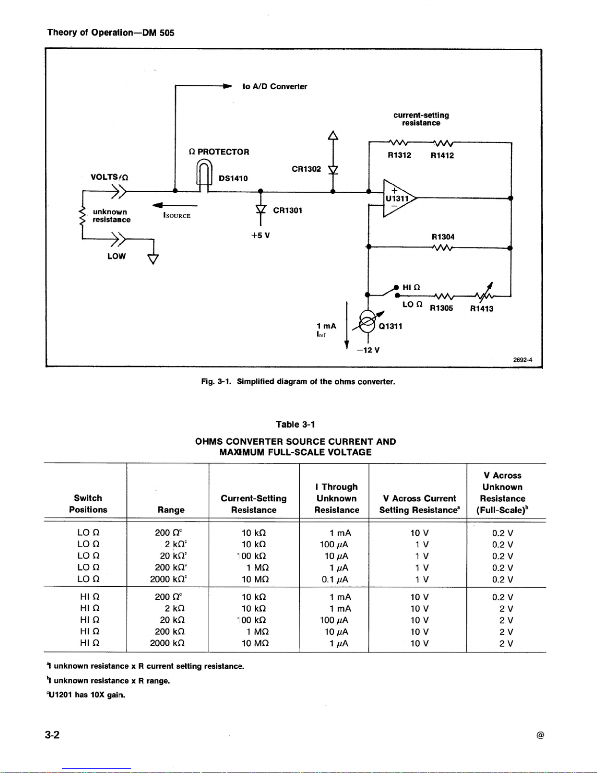
The ohms converter consists of precision current
source
01 31 1
and
floating current mirrar U1311 (see Fig.
3-1). Transistor Q1311 generates a relatively low
temperature coefficient current,
by
mirroring the voltage
from
Zener diode VR1211 across R1215 and R1213.
The
current at
the
collector
of
Q1311 E is approximately
i
rnA
and is adjusted by R1213, the
HI
fl
ADJ.
This
reference
current
from
Q1311 B appears at the inverting terminal
of
U1311. The output of Q1311 sources current through
R1304 to stabilize the reference current. In the HI
R
position, the output
of
U1311 is elevated 10 V above its
input. In the
LO
R
position,
S2-H
connects R1305 and
R1413 in parallel with R1304, lowering the
output
voltage
of
U1311 and reducing thereferencecurrent to U1311 pin
2
by
a
factor of 10. Table 3-1 lists the values
of
source
current for the resistance ranges in the HI
il:
and LO
R
positions. Resistor R1413 adjusts the
LO
reference
current to one-tenth
of
the
HI
Cl
reference current.
Page 30
Theory
of
Operalton-DM
505
I
>
to
A/D
Converter
curred-Wing
reQstance
n
PROTECTOR
~1312 131412
CR1302
VOLTSlR
OS1410
unknown
ISOURCE
CRf
SO1
resistance
+5
V R1304
LOW
tll
R
I
mA
lr
ci
26924
J
Fis
3-1.
Simplified diagram
ol
the
ohms converter.
Table
3-1
OHMS
CONVERTER
SOURCE
CURRENT
AND
MAXtMUIYI
FULLSCALE
VOLTAGE
.I
unknown
reslstame
x
R
current
setting
resistance
9
unknown
resistamce
x
R
range.
%I1201
has
1OX
galn.
Swltch
Positions
LO
Sl
LO
n
LO
12
LO
R
LO
R
HI
R
HI
n
HI
R
HI
R
HI
R
Range
---
200
flc
2
k~'
2Q
kRG
200
kQc
2000
kRc
200
RE
2
kn
20
kR
200
kR
2000
kR
Current-Setting
Resistance
I
Through
Unknown
Resistance
10
kR
10
kn
100
kR
1
MR
10
Mfl
10
kR
10
kn
100
kR
1
Mfl
10
MR
V
Across
Current
Setting
Resistance'
V
Across
Unknown
Resistance
(Full-S~ale)~
1
mA
100
PA
10
PA
1
PA
0.1
pA
1
mA
1
m~
100
PA
10
PA
1
PA
10
V
tv
1
V
f
V
1
V
10
V
10
v
10
V
10
V
10
V
0.2
V
0.2
v
0.2
V
0.2
V
0.2
V
0.2
V
2v
2V
2V
2V
Page 31

Theory
of
Operation-DM
505
The output voltage of
U1311
is applied across sections
of
the
attenuator
R1312
(and
R1412for
the
200
kn range)
which
serves
as a current setting resistance. The voltage
across
R1312
and
R1412
is equal to
the
voltage
across
R1304.
The current through
R1312
flows through lamp
DS1410
and out
the
VO
LTS/R terminal through the
unknown resistance. The range switches select sections
of
the attenuator
so
that different values of current can
be
sourced out
of
the VOLTS/I1 terminal.
The
voltage
developed across the unknown resistance
is
then
measured by the
ASD
converter.
Diodes
CR1301
and
CR1302
and
lamp
DSt4lO
protect
the
ohms converter from
excessive
dc
and
ac
input
voltages. If
an
excessive voltage is applied to a resistance
range, the voltage is clamped by
CR1302
and
GR1301
and
appears across lamp
PS1410.
As
the filament
of
DS1410
warms
up,
the rmistance of thefilament increases, limiting
the current through the diode clamps.
DS1410
is rated
to
handle
125
V
rms indefinitely and
250
V
rms for a Fimited
time. Voltages in
excess
of these ratings cause
DSI410
to
act
as a
fuse. Diode
CR1301
also limits
the
open
circuit
voltage
at
the VOLTS/R input connector to approximately
+6
V.
Current
Shunts
@
The
current shunts in the
DM
505
consist of
R1425,
Rl426,
and t hick-film resistor network
R1521,
connected
between
the
mR
and LOW input terminals.
These
resistors
convert the input current to
a
voltage for measurement by
the
DM
505
circuitry. The maximum full
scale
voltage
developed across the current shunts
at
the
maximum full
scale current
is
0.2
volt. In the
dc
current mode, this
voltage is switched directly to the
ND
converter. In the ac
current
mode,
the current shunt voltage is first routed
through the
ac converter. The current shunts
are
protected by the diodes in
CR1621.
If
the
voltage across
the current shunts exceeds approximately
1.2
V,
the
diodes in
CR1621
begin
conducting, shunting current
around the resistors. The maximum voltage drop across
the current shunts in
an
overload condition is
ap-
proximately
1.5
V.
An input current exceeding
2
A opens
fuse
F1521.
The
DM
505
measures
voltages
up to
1
kV
peak above
chassis
ground
(200
V
peak above ground
at
the rear
interface input). Isolation
is
accomplished with power
transformer
Tl001,
which is powered from
the
25
Vac
floating windings
13A
and
138
of the power module.
Transformer
Kl 001
converts the
25
Vac to a secondary
output of
47
V
rrns, center-tapped, across pins
7
to
9,
and
12
V
rms across pins
lOto 12.
The 47 Y rms is rectified
by
CR1111
and filtered by capacitors
C1012
and
Clll
f
to
provide approximately + and
-
26
V
unregulated. The
positive voltage across
ClOl2
is
regulated
to
+15.75
V
by
U1022,
and
shunt resistors
R1122
and
R1021.
Resistor
R1021
adjusts the output voltage
for
the
minimum
+15.75
V required for proper ohms converter operation.
The
negative
voltage
across
Cllll
is
regulated to
-12
V
by
Uf 121.
The
current pulled from
each
of these supplies
is approximately
40
rn
A.
Capacitor
C1021
equalizes un-
balanced capacitance between the secondary windi ngs of
T1001,
pins
7,
8, and
9.
Capacitor
C1021
reduces any
60
Hz
common
mode
signal appearing between the front
panel input terminals of the
DM
505
and chassis ground.
The
12
V
rrns
from the secondary
of
TI
001,
pins
10
to
12,
is rectified
by
CRfOll
to provide approximately
+I2
Y
unregulated to the display anode drivers. The
+12
V
across
ClOf
I
is regulated to
+5
V
by
U1021.
Clock
9
The clock signals for
U1303
are generated
by
U1301,
a
free-running multivibrator
wit
h
a
frequency determined by
C1203, R1205, R1204,
and
R1202.
CLOCK
FREQ
ADJ
R1202
sets the clock frequency to
20.48
kHz,
a
multipEe
of
the
line frequency. Components
of
50
Hz or 60 Hz
at
the
input terminals are rejected since they
are
of
equal
magnitude during the up and down portions
of
the
measurement cycle,
Analog
to
Digital Converter
@
Integrated circuit
U1201
comprises
the
analog section
of the analog-to-digital
(#D)
converter
and
U1303
con-
tains the necessary control logic.
The
A/D
converter in the
DM
505
operates
on
the charge balancing principle. The
input voltage is converted to
a
current that charges
capacitor
Cf 101
in an integrator circuit. Charging con-
tinues until the capacitor voltage crosses afixedthreshold
level. Then
a
reference current larger than
the
maximum
input current
is
subtracted from the input current and the
capacitor discharges until
the
threshold level is crossed
again. This process
is
repeated until the measurement
interval is over. During the measurement interval,
a
counter in
U1303
accumulates clock pulses from clock
generator
U1301
when only the input signal
is
applied to
the integrator,
and
subtracts clock pulses
when
both the
input
signal and the reference current are applied to
the
integrator, resulting in a net count proportional to the
input voltage. This conversion occurs in
U1201
and
is
controlled
by
U1303.
Refer
to
Fig.
8-2
in the Diagrams
section.
Integrated circuit
U1201
also contains automatic zero-
ing
circuitry. Between meaurement intervals, the input of
U1201
is
switched to ground and an auto-zero voltage,
related
to
the offset voltages
in
U1201,
is stored across
auto-zero capacitor
C1102.
This auto-zero voltage is
converted to
a
current and subtracted from the input
current
at
the integrator
so
that errors due to
offset
Page 32

Theory
of
Operalion-DM
SO5
voltages and ground offsets are compensated.
The
reference voltage for
U1201
is
supplied
by
a
temperature
stable diode,
VR1201.
Resistors
R1111
and
R1112
(the
2
Vdc
ADJ)
convert the
reference
voltage
to
a
reference
current
for
the integrator, The gain of the integrator is
switchable from
one
to
ten
by
placing
R1210,
R1211,
and
R1301
in parallel with
R1212.
This gain increases
the
integrator input current derived from the input signal by
a
factor
of
ten. Resistor
R1210
allows the total parallel
resistance
to
be
closely trimmed for proper
gain
for the
200
mVdc
range. Resistor
R1113
and
low-leakage diodes
CR1113
and
CR1112
provide input protection for
U1201.
Capacitor
C1201
and resistor
R1113
increase the normal
mode rejection
of
U1201.
Transistor
Q1201
and
DC
ZERO
ADJ
resistor
R1104
set the dc zero of
Ut201,
Integrated
circuit
U1201
receives commands from
U1303
via two
digital linescalled "measure-zero"
(U1201,
pin
3)
and
"up
down"
(U1281,
pin
4).
The
"up-down" line controls the
direction
of
counting and integration.
The
"'measure-
zero" line determines whether
the
input
of
U1201
receives
the input signal or is connected
to
ground. Integrated
circuit
U1201
provides an output
to
U1303
through
a
"comparator" line
(U1201,
pin
5).
The comparator line
signals the counter in
U1303
when
the integrator has
passed the threshold. The outputs
of
U1303
control the
d~splay through
the
display driver circuitry.
A
detailed description
of
the operation of the
A/D
converter follows.
The
20.48
kHz clock frequency from
U1301
is divided
by
the time
base
counter
into
groups
of
6144
pulses.
Measurement takes place
for
4096
of
these
pulses and
automatic zeroing
takes
place for
2048
pulses.
During
the
auto zero interval, the input of the buffer
amplifier is grounded.
The
buffer offset current also
offsets the
output
of
the integrator.
The
offset
at
the
integrator output passes through
R1103
to
the
plus input
of the auto-zero amplifier.
The output
of
the
unity gain
auto-zero amplifier compensates for this offset current at
the summing node (pin
9)
at the integrator input. The
reference current through
Rl
f
11
and
R1112
from the
reference voltage source is applied for four clock cycles
and disconnected for the next four cycles by the
U/D
control logic. The reference current is connected to
R1112
when the updawn logic is low. Equilibrium
for
the
entire
integrating
and
auto-zero system is obtained when the
sum
of
the average currents at the integrator summing
junction
equals zero. Capacitor
GI102
charges to the
equilibrium voltage and maintains this
voltageat
the
auto-
zero amplifier input during
the
measurement interval
when the switch from the integrator output is
open.
See
Fig.
3-2
for functional timing during theauto-zerointerval.
The
fifty percent
duty
cycle
of
the
up-down
counter
is
overridden
at
the
start of
the
auto-zero interval. This
override period permits the output of the integrator to
come
to
V,, and
Cf
102
to
assume this
voltage.
Fig.
3-2.
Auto-zero
timing intervals.
I
d
.
YOVERRiDE
r
1
AUTO-ZERO
-
U/D
I
I
1
COMPARATOR
I
I
1
I
1
INTEGRATOR
OUTPUT
2692-5
Page 33
Theory
of
Operation-DM
505
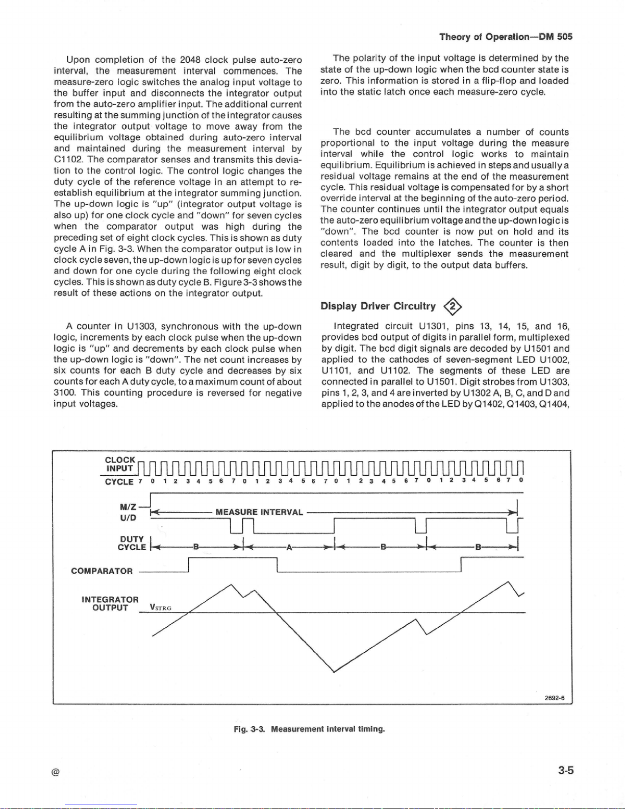
Upon completion of the
2048
clock pulse auto-zero
interval,
the
measurement interval commences.
The
measure-zero logic switches the analog input voltage to
the
buffer
input and disconnects the integrator
output
from the auto-zero amplifier input.
The
additional current
resulting at the summing junction of theintegrator
causes
the integrator output voltage to
move
away from the
equilibrium voltage obtained during auto-zero interval
and
maintained during the measurement interval
by
C1102.
The
comparator senses and transmits this devia-
tion to
the
control logic.
The
control logic changes the
duty cycle of
the
reference voltage in
an
attempt
to re-
establish equilibrium at the integrator summing
junctfon.
The
up-down logic
is
"up" (integrator output voltage is
also
up)
for
one
clock
cycle
and
"down" for seven cycles
when the comparator output
was high during the
preceding set of eight
clock cycles.
This
is
shown
as
duty
cycle
A
in Fig.
3-3.
When
the
comparator output is
low
in
clock cycle
seven,
the up-down logic
is
up
for
seven
cycles
and down for
one
cycle during the following eight clock
cycles.
This
is
shown
as
duty cycle
B.
Figure3-3 showsthe
result
of
these actions on the integrator output.
A
counter in U1303, synchronous with
the
up-down
logic, increments by
each clock pulse when the up-down
logic is
"up"
and
decrements
by
each
clock pulse when
the up-down
Iogic
is
"down".
The
net
count increases
by
six
counts
for each B duty cycle and decreases by six
counts for
each
Aduty cycle, toa maximum count
of
about
3100.
This
counting procedure is reversed
for negative
input voltages.
The
polarity
of
the input voltage is determined by the
state
of
the
updown
logic
when
the bcd counter state is
zero. This information
is
stored in a flip-llop and
loaded
into
the
static latch Once
each
measurezero cycle.
The bcd counter accumulates a number of counts
proportional to the input voltage during the measure
interval
while
the
control logic works
to
maintain
equijibrium. Equilibrium is achieved in
steps
and usual1 ya
residual voltage remains
at
the
end
of the measurement
cycle.
This
residual voltage is Compensated for by a short
override interval at
the
beginning
of
the auto-zero period.
The
counter
continues
until the integrator output equals
the auto-zeroequilibrium voltageand the up-down logic is
"down".
The
bcd
counter is
now
put
on
hold and its
contents
Zoaded into the latches. The counter
is
then
cleared and
the
multiplexer sends the measurement
result, digit
by
digit,
to
the
output
data
buffers.
Display
Driver
Circuitry
@
Integrated circuit
U1301,
pins
13,
14,
15,
and 16,
provides
bcd
output of digits
in
parallel form, multi;plexed
by digit.
The
bcd digit signals are decoded by
U1501
and
applied
to
the cathodes
of
seven-segment
LED
Uf
002,
U1101,
and U1102.
The
segments of these LED are
connected
in parallel
to
U1501. Digit strobesfrom U1303,
pins
7,2,3,
and 4 are inverted by U 1302
A,
B,
C,
and D and
applied to the anodesof the
LED
by Q1402, Q1403, Q1404,
CLOCK
INPUT
CYCLETO
r2
345s
70
12345s
71
9
Z~~SB~O
12
34s
et
o
MI'
u/a
4-
MEASURE
INTERvM
c"Y"CyE
LdAA&
B-1
COMPARATOR
I
I
I
INTEGRATOR
OUTPUT
VS~RG
269M
Fig.
3-3.
Measurement
Interval
timing.
Page 34

Theory
of
Operation-DM
505
and Q1405.
The
segment
information at
the
cathode
of
each
LED
is displayed
as
its anode is strobed high.
The
display
is strobed
in
the
following
order:
digit
1,3,2,
and
4.
Digit
f
is
the
least
significant and digit 4 is
the
most
significant (1
or
0). The
digit strobes are also routed
through
sections
of
the
range switches
to providedecimal
point
information to
the
display. Transistor
Q1507
con-
trols the most signifFcant digit, U1001.
The
sign
is enabled
by
switches
S2K
and
S2B,
which
connect
thesign
anodes (t11001
pins
1,6,and7) to+12
V.
The
cathode
of
the
negative
segment
of
the
sign (pin
4)
is
hard-wired
low
through
R1601.
The
sign
of
the
input
from
U1303,
pin
5,
is
buffered through U1302Etothe
cathodes
of
the
positive
segments
of the
sign
(U1001,
pins 3 and
5).
If
the
sign
has
been
enabled
by
S2K
or
S2B, a positive
sign
will
be
displayed
when
pins
3
and 5 are low.
Page 35

CALIBRATION
PROCEDURE
lntroductlon
Test
Equi
pent
Requirements
This section consists of a Performance Check which
Below
is
a
list
of
equipment required to verify operation
verifies the electrical specifications
listed in Section
1,
and
as specified Other equipment
may
be
substituted when
an Adjustment procedure which provides
a
sequential suitable.
adjustment
of
internal controls. This procedure should
be
used
to
restore
the
instrument performance
to
the etec-
trical specifications listed
En
Section
1
of
the manual.
Table
4-1
LIST
OF
TEST
EQUIPMENT
REQUIREMENTS
Description
TM
500
Pawer
Module
Periormance
Requirements
Dc
voltage
accuracy
check
fluke Model
341A
Voltage
source within
f
0.01%
De
common
mode
rejection check Cali brator
2
Ydc
range adj ustrnent
200
mVdc
range adjustment
Applications
All
steps
Ac voltage
source
Example
TEKTFIONIX TM
501,
TM
503,
TM
504,
TM
506
OV
to
500
Vrms,
25
Hz
to
20
kHz,
within
50.05%
Ac
voltage
accuracy
check
Dc
common mode rejection check
Dc
normal
mode rejection check
Ac
common
mode
rejection check
2
Vac
range
adjustment
200
mVac
range
adjustment
10
kHz
ac
adjustment
---
Resistance
standard
Dc
current source
Ac current source
1
kS2
resistor
Fluke Model
5200A
Ac
Voltage
Cali brator and
Fluke
Model
521
5A
Power
Amplifier
Ohms
accuracy
check
HI
fl
adjustment
LO
i2
adjustment
pppp
Dc
current accuracy
check
o-
Ac
current
accuracy
check
Dc
common
mode
rejection check
Ac common
mode
rejection check
---
+15.75
V
supply adjustment
Clock frequency adjustment
0
R
to 2 Mn,
within
f
0.05%
0
A
to
2
A,
within
f
0.0Ph
0
A to
2
A,
45
Hz to
10
kHz,
within
f
0.15%
3%
tolerance,
1
J8
watt
Electro Scientific Industries
Model
DB62
Decade Resis-
tance Box
Valhalla
Scientific
Inc.
Model
2500
AGDC
Cur-
rent
Cali
brator
Same
as
for
dc
current
Tektronix Part
No.
321-01
93-00
f
EKTRONIX
DM
501
A,
DM
502,
DM
502A
TEKTRONIX
DC
504, Digital
Counter
Voltmeter
Counter
0
to
+20
V,
1
mW
resolution
20.48 kHz, within
&0.25%
Page 36
Calibration
Procedure
(Performance
Check)-DM
505
Table
4-1
(cont)
on
mode rejection
check
tronix
Par!
No.
c
common
mode rejection
check
Tektronix
Part
No.
dual
banana
Dc
normal
mode
rejection
check
Tektronix
Pad
No.
01
3-007&00
connector
I
ea
bnc
female
to
clip
lead
adapter
2
ea
coaxial
cable
with
bnc
connectors
Tektronix
Part
No.
01 2-0057-01
Ac
common
mode
rejection
check
Ail
accuracy
checks
Dc
common
mode
rejection
check
Ac
common
mode rejection
check
1
ea
dual
banana
shorting
bar
Cable
50
n
irn pedance
Dc
zero
adjustment
Ac
zero
adjustment
For
connection
to
instrument
under
test
Adjustments
Clock
frequency
adjustment
Tektronix
Part
No.
067-0645-02
Tektronix
Part
No.
01
0-61
01-01
Page 37

Calibration Procedure (Performance
Check)-DM
505
PERFORMANCE
CHECK
Introduction
2.
Install
theDM
505inthepowermoduleandconnect
This procedure
checks
the electrical characteristics
of
the power module and test equipment
to
the line voltage
the
DM
505
that appear
in
the Specification portion
of
this
source.
manual. If the instrument fails
to
meet
the
requirements
given
in
this
Performance Check, the Adjustment
procedure should
be
performed.
3.
Turn
on
the power module
and
all test equipment
and
allow
at
least
30
minutes
for
warm-up
(60
minutes
after
storage in
a
high
humidity environment).
The
electrical characteristics in this section
are
valid
only if the
DM
505is calibrated at anambienttemperature
between
+21°C
and
+25"C
and operated at
an
ambient
temperature between
0'
C
and
f
50°C.
Tolerances that are specified in this Performance
Check apply
to
the instrument under test and
do
not
include test equipment
error.
For
convenience,
many
steps in this procedure check the performance
of
this
instrument
at
on1
y
one
value
in
the
sgecif
ied
performance
Dangerous
voltages
may
be
encounfered
in
the
following
sfeps.
Caution
must
be
exercised.
Do
not
contact
the
output
connectors
of
the
voEtage
calibrator,
the
input
terminals
of
the
DM
505
or
the
jnternal
circujtry
of
the
DM
505.
The
knobsetscrews
of
soma
voftage
calibrators
have
Been
known
to
be
af
a
high
voltage
potential;
check the
setscrews with
a
voltmeter
before
handling
the
knobs.
range. Any value, with appropriate limits, within the
FRONT
PANEL
PERFORMANCE
CHECK
specified range may
be
substituted.
PROCEDURE
For the following sections
of
the Performance
Check,
set
the
INPUT
EXT-INT pushbutton
to
the
out
(EXT)
If
the
rear interface input
is
to
be
used,
the rear interface
position.
accuracy specifications for
ac
and
dc
voltages and
resistances may
be
checked using
aTM
500-series Option
2
power
module. Instructions and accuracy tables for rear
1-
Check
the
~c
voltage
Accuracy
interface performance check are given following this
procedure.
a.
Set the
dc
voltage calibrator to
0 V and connect the
dc
voltage calibrator through the
necessary
adapters
and
the
50
R
coaxial cable to the
VQLTS/R
and
LOW
input
connectors.
Preliminary
Procedure
1.
Ensure
that
all
power
switches
are
off
and that the
b. Press
the
VOLTS
DC
button
and
set
the calibrator
power module
and
all test equipment are adapted for the
voltages and the
DM
505
range pushbuttons
as
listed in
line
voltage
available. Table
4-2.
TaMe
4-2
DC
VOLTAGE
ACCURACY
DM
505
Range
Button
200
mV
2
V
20
V
200
V
1000
V
Dc
Calibrator
Display
Umlts
Voltage
+IS0
C
to
3-28"
C
0
to
+lB°C,
+2a°C
to
+50°C
pp
180.000
mV
1.80000
V
18.0000
V
180.000
V
1000.00
V
179.7
to
180.3
1.797
to
1.803
17.97
to 18.03
179.7
to
180.3
998
to
1002
179.4
to
180.6
1.794
to
1.806
17.94
to
18.06
179.4
to
180.6
996
to
1004
Page 38

Calibration
Procedure
(Performance
Cheek)-DM
505
c.
CHECK-that the
DM
505
display reads within
the
g
Check
Common
Mode
Rejection
(PC
Mode)
limits
for
the
ambient temperature
as
listed
in
Table
4-2.
a.
Connect
the
bnc female
to
dual banana
connector
to
the
VOLTS/R
and
LOW
connectors.
d.
Set
the
dc
calibrator output voltage to
0
V
and
disconnect it from
the
DM
505.
b. Connect
the
bnc male to dual binding
post
connec-
tor to
the
bnc
female
connector attached to
the
DM
505
front panel.
2
Check
Ac
Voltage
Accuracy
a.
Set
theacvoltagecalibrator to0 Vandconnectthe
ac
voltage calibrator
(and
power ampiifier,
as
needed)
to
c.
Connect
the
1
kR
resistor between the binding
the
VOLTS/R
and
LOW
input CQnneCtOrS through the
posts on the dual binding post connector.
coaxial cable
and
necessary adapters.
b. Press the
VOLTS
AC
button, Press
the
range
d.
Connect the red clip lead
of
the
bnc
female
to
clip
buttons and set
ac
calibrator voltage
and
f
requenc~
as
lead adapter to
the
red binding
post
and
the
black
cli
p lead
listed in Table
4-3.
to
the
DM
505
ground binding post.
c.
CHECK-that the
DM
505
display reads within the
e.
Connect the
bnc
female connector through
a
coax-
limits
tor
the
ambient temperature
as
listed in Table
4-3.
ial cable
to
the dc voltage calibrator.
d.
Set
the
ac
calibrator output voltage
to
0
Y
and
disconnect it from the
DM
505.
f.
Press
the
VOLTS
DC
and
200
mV
pushbuttons.
Table
4-3
AC
VOLTAGE
ACCURACY
45
Hz-1
0
kHz
1.779
to
1.821
17.79
to
18.21
Page 39

Calibration
Procedure
(Performance
Check)-DM
505
g.
Set
the
dc
voltage
calitxator
for
an
output
of
100
Vdc.
d.
Connect
the
red
clip
lead
of
the
female
bnc
to
clip
lead adapter
to
the
red binding post
and
the
black
clip lead
to
the
DM
505
ground binding post.
h.
CHECK-that the display reads
G01.0.
e.
Connect
the
female
bnc connector through
a
coax-
ial
cable
to
the
ac
voltage calibrator.
i.
SetthedcvoltagecalibratortoOVBndreconnectthe
coaxial cable
to
the
ac
voltage calibrator.
f.
Press
the
VOLTS
AC
and
200
mV
pushbuttons.
j.
Set
the
acvoltage calibrator
for
an
output
of
50
Vac
rms
ai
50
to
60
Hz.
g.
Set
the
ac
voltage
calibrator for
an
output
of
5
Vac
rms
at
50
Hz
to
60
Hz
+0.2
Hz.
k.
CHECK-that
the
display
reads
G7.2.
h.
CHECK-that
the maximum
display
reading is
G22.4.
I.
Set
the
ac
voltage calibrator
output
to
0
V
and
disconnect it from the
DM
505.
i.
Set
the
ac
voltage calibrator output to
0
V
and
disconnect it from the
DM
505.
NOTE
If
the
DM
505
does
not
display
the
correct
readings
as
stated
in
step
3
parts
h
and
k,
perform
Clock
5.
Check
Normal
Mode
Rejection
(Dc
Mode)
Adjustment
of
the
Adjustment
procedure
andrepeat
the
above
Common
Mode
Rejection
Check
(Dc
a.
Connect
the
bnc
female
to
dual
banana
connector
Mode).
to the
VOLTS/R
and
LOW
connectors.
b.
Attach the
bnc
connector through a coaxial cable to
the
ac
voltage
calibrator.
4.
Check
Common
Mode
Rejection
(Ac
Mode)
c.
Press the
VOLTS
DC
and
200
mV
pushbuttons.
a.
Connect
the
bnc female
to
dual banana connector
to
the
VOLTS/R
and
LOW
connectors.
d.
Set
the AC Calibrator for 0.224V AC at 50Hz *0.2Hz
or
60Hz *0.2Hz.
b.
Connect the bnc male to dual binding post connec-
tor
to
the
bnc
connector
attached to
the
DM
505
front
e.
CHECK-that the maximum display reading
is
panel.
G
1.0.
c.
Connect
the
1
kR
resistor
ktween
the
binding
f.
Set
the
ac
calibrator output
to
0
V
and
disconnect it
posts
on
the
dual
binding
post
connector.
from the
DM
505.
REV A OCT
1979
Page 40

Caribratlion Procedure
(Performance
Check)-'DM
505
6.
Check
Ohms
Accuracy
a.
Connect
the resistance
standard
to the
VOLTS/Rl
and
LOW
connectors.
b.
Press
the
kf2
pushbutton.
Make
each measurement
in
thefollowing
tablewith the
HI
!2-LO
R
button
in
the
LO
(in)
and
the
HI (out) positions.
c.
CHECK-that
the
display
reads within the limits
for
the
ambient tern
perature
as
listed
in
Table
44.
d.
Remove
all
connections
to
the
DM
505.
7.
Check
PC
Current
Accuracy
a.
Connect the
current
calibrator
output
through
a
coaxial cable
and
necessary
adapters tot
he
mA
and
LOW
connectors.
Connect
the
dc
voltage
caPibrator
output
through
a
coaxial
cable
and
adapters
to
the
current
calibrator
input.
b.
Press
the
rnA
DC
button
and
set
the
DM
505
range
buttons
and
current
source
output
as
listed
in
Table
4-5.
c.
CHECK-that
the
display
reads
within
the
limitsfor
the ambient
temperature
as
listed in Table
4-5.
d.
Set
the dc current
source
to
0
A
and
disconnect
it
from
the
DM
505.
Table
4-4
OHMS
ACCURACY
I
I
Table
4-5
Range
Button
200
n
DC
CURRENT
ACCURACY
--
Standard
180.000
n
DM
505
Range Button
200
pA
2
mA
20
mA
200
m
A
2000
mA
.
.
%lB°C
to
+2a°C
178.8
to
181.2
Dc
Current
Source
180.000
pd
1.80000
mA
18.0000
mA
180.000
mA
1800.00
mA
0
to
S18"C,
f28"C
ta
+50°C
177.9
to
182.1
Display
Umlts
4-18' C to
f
28"
C
179.4
to
180.6
1.794
to
1.806
17.94 to
18.06
179.4 to
180.6
1794
to 1806
0
to
+18OC,
+2BDC
to
+50°C
179.0
to
181.0
1.790
to
1.810
17.90
to 18.10
179.6
to
181.0
1700
to
1810
Page 41

Calibration
Procedure
(Performance
Check)-DM
505
8.
Check
Ac
Current
Accuracy
a.
Connect
the
current calibrator outpul through
a
coaxial cable
and
the
necessary
adapters
to
the
mA
and
LOW
connectors. Connect
the ac
voltage calibrator
output
through
a
coaxial
cable
and
adapterstathe current
calibrator input.
b,
Press
the
mA
AC
button
and
set
the
DM
505
range
buttons
and
the
Current
source
output,
as
shown in Table
4-6,
at any frequency from
45
Hz
to
10
kHz.
c.
CHECK-that
the
display reads within the limits
for
the
ambient temperature
as
listed in Table
4-6.
d.
Set the current source to
0
A
and disconnect it
from
the
DM
505.
REAR
INTERFACE
PERFORMANCE
CHECK
PROCEDURE
f
o
verify instrument accuracy of resistance
and
ac
and
dc
voltage
modes via
the
DM
505
rear
interface,
followthe
steps outlined
in
the Performance
Check
procedure
for
the
f
ront
panel input, but apply voltages and resistances to
rear interface pins
28B
(HI)
and
28A
(LO).
Access
to
the
rear
interface
input
pins
28A
(LO)
and
28B
(HI)
is
most
easily
made
using
a
TM
500-series
Option
2
power
module. Press the
INPUT
EXT-INT pushbutton (INT
position) to select rear interface input. Substitwte Tables
4-7, 4-8,
and
4-9
for
the
appropriate
tables
listed
in
the
Performance
Check
procedure.
NOTE
The
inprrf
cable
fixture
from
the
calibrating
sources
to
the
rear
interface
pins
will
have
fo
be
modified
to
accommodate
accuracy
checks
via
the
rear
interface.
Table
4-6
AC
CURRENT
ACCURACY
Table
4-7
DC
VOLTAGE ACCURACY
FOR
REAR
INTERFACE
DM
505
Range
Button
-
200
pA
2
mA
20
mA
200
m
A
2000
m
A
Ac
Current
DM
505
Range Button
200
rnV
2
Y
20
V
200
V
1000
V
(max.
input
200
V
peak)
Display
Umits
Dc
Calibrator
Source
4-18"
C
to
-t2e°C
O
to
+18OC,
+28*
C
to
+50°
C
pppp
Display
LFmits
180.000
pA
1.80000
mA
18.0000
mA
180.000
rn
A
1800.00
mA
Volt
age
180.000
mV
1.80000
V
18.0000
V
180.000
V
180.000
V
178.5
to 181.5
1.785
to
1.815
17.85
to 18.15
f
78.5
to 181.5
1785
to
1815
177.5
to
182.5
1.775
to
1.825
17.75
to
18.25
177.5
to
182.5
1775
to
1825
+I
8O C to
+28O
C
179.7
to 180.3
1.797
to
1.803
17.97
to
18.03
179.7
to
180.3
178 to
182
0
to
+lR°C,
+28"C
to
-1-50°C
179.4
to
180.6
1.794 to 1.806
17.94
to
18.06
179.4 to 180.6
177
to
183
Page 42
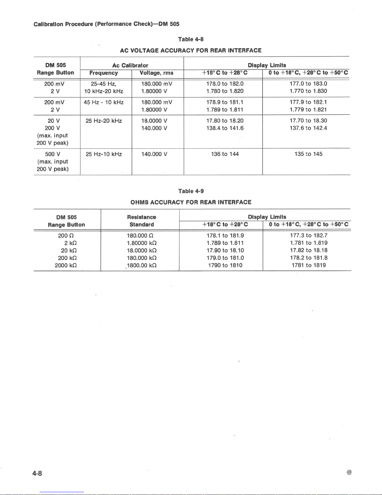
Callbratlon
Procedure
(Performance
Cheek)-DM
505
Table
4-8
AC VOLTAGE
ACCURACY
FOR
REAR INTERFACE
10
kHz-20
kHz
f
.?80
to
f
,820
1.770
to
1.830
fable
4-9
OHMS
ACCURACY
FOR
REAR
INTERFACE
OM
505
Range
Button
200
R
2
kR
20
kn
200
kfl
2000
kfl
Resistance
Standard
180.000
R
1.80000
kfl
1
8.
OQOQ
kfl
180.000
kR
1800.00
kR
Display
Llmlts
+I
8"
C
to
+2B0
C
178.1
to
181.9
1.789
to
1.811
17.90
to
18.10
179.0
to
181.0
'I790
to
1810
0
to
+lB°C,
+2R°C
to
i-50°C
177.3
to
182.7
1.781
to
1.819
17.82
to
18.18
178.2
to
181.8
1786
to
1819
Page 43

Callbration
Procedure
(Adjustments)-DM
505
ADJUSTMENTS
Introduction
PROCEDURE
This procedure need
not
be
performed
unless
the
instrument fails
to
meet the performance requirements
of
I-
Adiwt
the
+15m7S
the electrical characteristics listed in the Specification
a.
Set
the voltmeter to the
20
Vdc
range.
section. Adjustment
is
generally required after a repair
has
been made or after long time intervals
in
which normal
aging
of
components
may
affect instrument accuracy.
b. Connect the voltmeter positive lead to the DM
505
H5.75
V
tea point
and
the negative lead to
TP1521
(LO).
To
ensure instrument accuracy, check
the
calibration
every
1000
hours
of operation or
every
six
months if used
c.
EXAMINE-that the voltmeter reads
+15.75
Vdc
infrequently.
f
0.08
V.
Tektronix, I
nc.
provides complete instrument repair
d.
ADJUST-R1021,
the+15.75 V ADJ,for avoltmeter
and
calibration at local Field Service Centers
and
at
the
reading
of +15.~5
v
f0.05
V.
Factory
Service Center. Contact your local Tektronix Field
Office
or
representative for
further
information.
e.
Disconnect the voltmeter from the
DM
505.
Test
Equlpmeml Required
2.
Adjust
the Clock
Frquency
Test equipment used for adj ustrnent of the
DM
505
is
a.
Set the counterto Frequency,
10
Hz
Resolution, and
listed
in
the beginning of the Calibration
section.
All test
Display
Time
fully
ccw.
equipment is assumed to
be
correctly calibrated
and
operating within specifications.
b.
Connect the counter input lead
to
the
CLK
test
point.
A
XI
probe
may
be
used,
if
desired.
Preparation
Connect
the
DM
505
to the power module via the
flexible
plug-in extender.
To
gain
access
to
the
ad-
justments,
remove
the left side cover
of
the
DM
505
by
pulling the
rear
of the side cover
outward
from
the
instrument. Then remove the large
metal
shield attached
to
a
standoff in
the
center of
the
instrument. If desired,
most
adjustments may be made through the holes in
the
metal
shields using an insulated adjustment tool. Adjust-
ment locations
are
shown in the illustration located in
the
pullout
pages
at
the
rear
of
this manual.
Connect the test equipment
and
the
power
module to
a
suitable line voltage source. Turn on the
power
module
and the test equipment;
allow
at
least
30
minutes far
equipment
warm
up
and
stabilization. Set the
INPUT
EXT-
INT to the out
(EXT)
position.
Make
adjustments at an
ambient temperature
of
+21°C
to
+25*C.
Perform
ad-
justments in the order given, since
some
adjustments
interact with others. Interactions
are
noted
in the
procedure.
Refer
to the adjustment location
page
(in the
Diagrams and
illustrations
section).
c.
EXAMINE-that the counter reads
20.68
kHz
to
20.28
kHz.
d.
ADJUST-R1202,
CLOCK
FREQ
ADJ,
for a fre-
quency of
ZQ.48
kHz
rt0.05
kHz.
e.
Disconnect the
counter.
3.
Adjust
Oc
Zero
a.
Press the
VOLTS
DC
button and the
200
mV range
button.
b.
Short
the
VOLTS/n
and
LOW
input connectors
together with the dual
banana
plug
shorting bar.
c.
EXAMINE-that the
DM
505
display reads
00.0
rto.
1.
Page 44
Callbratlon Procedure (Ad1ustmenls)-DM
505
d. ADJUST-R1104, DC
ZERO
ADJ,
for a display
5.
Adjust
the
200
mVdc
Range
reading
of
00.0
M.
a.
Set
the
dc
voltage calibrator to 0.190
V.
e. Press the
2
V
range
button.
b.
Press the VOLTS
DC
button and the 200
rnV
range
button.
f.
EXAMINE-that the
DM
505
display reads .000
40.001.
c.
Connect
the
voltage calibrator positive lead to the
VOLTSJQ connector
and
the
negative lead to the
LOW
g.
ADJUST-R1104
for
a
display
reading
af
.000.
connector.
NOTE
d.
EXAMINE-that
the
DM
505
display reads 190.0
f
0.3.
Best
results
will
be
obtained
with
R1104
set
mid-way
in
the
range
for
which
both
the
200
mV
and
2
V
DC
scales
read
0.
e.
ADJUST-R1210,
.2
VDC
ADJ,
for a reading
of
190.0
310.1.
h.
INTERACTEON-this adjustment
affects
the
AC
VOLTMETER
zero and most other f ull-scale adjustments.
f.
INTERACTION-this adjustment
affects
the
200
mVac
and
LO
R
range adjustments.
i.
Disconnect the
short
between
the
VOLTS/R and
LOW input connectors.
4. Adjust
the
2
Vdc
Range
g.
Set
the voltage calibrator output
to
0
Y
and dis-
connect it from the
DM
505.
a.
Press the
VOLTS
DC
button
and
the
2
V
range
button.
6.
Adjust
the
HI
R
b.
Set
the
dc
voltage caFibrator
to
1.900
Y.
a.
Press
the
k!2
button, the HI
R
button
and
the
2
kR
range
button.
c.
Connect
the
calibrator positive
lead
to
the
VOLTS/R
b,
Set
the resistance standard
to
1.900
kn.
connector
and
the
negative lead
to
the
LOW
input
connector.
c.
Connect
the resistance standard
to
the
VOLTS/R
and
LOW
input connectors.
d. EXAMINE-that the
DM
505
display reads 1.900
d.
EXAMINE-that the
DM
505
display reads
1.900
*0.011.
e. ADJUST-R1112, the
2
YDC
ADJ,
for
a
display
reading
of
1
900
&0.001.
e.
ADJUST-R1213, the HI
fl
ADJ
for a display
readlng
of
1.900
f
0.001.
f. I NTERACTI ON-this adjustment
affects
the
200
mV
dc range, the HI
and
LO
n
and
both
AC V
range
adjustments.
f. INTERACTION-this adjustment
affects
the
LO
R
range adjustment.
g.
Set
the
dc
voltage calibrator output
to
0
V
and
disconnect it
from
the
DM
505.
g.
Continue
to
the
next
step.
Page 45
Callbration Procedure (Adjudments)-DM
505
7.
Adjust
the
LO
fl
a.
Press
the
kR
button, the
LO
Cl
button
and
the
2
kfl
range button.
c.
Connect the
ac
voltage calibrator to
the
VOLTS/il
and
LOW connectors.
d. EXAMINE-that the
DM
505
display reads
1.900
*0.012.
b.
EXAMIiq4E-that the
DM
505
display reads
1.900
*
0.01
1.
e.
ADJUST-R1322, the
2
VAC
ADJ,
for
a
display
reading
of
1
.W0
3.0.001.
c.
ADJUST-Rl413,
the
LO
R
ADJ, for a display
reading
of
1.900 f 0.001.
d,
Disconnect
the
resistance standard.
8.
Adjust
the
Ac
Zero
a.
Press the VOLTS
AC
button, and the
200
mV
range
button.
f,
INTERACTION-this adjustment
affects
the
200
mVac
and
10
kHz
ac
adjustments.
g.
Set
the
ac
voltage calibrator output to
0
V
and
disconnect it from
the
DM
505.
10.
Adjust
the
200
mVac
Range
a.
Press
the
VOLTS
AC
button and
the
200
mV
range
b. Short the
VOLTS/R and LOW input
connectors
button.
together
using
the dual banana plug
shorting
bar.
b.
Set
the
ac
voltage calibrator to
0,190
Vac
at
100
Hz.
e.
EXAMINE-that
the
DM
505
display reads
00.0
*
0.2.
c.
Connect
the
ac
voltage calibrator to the
VOLTS/R
and
LOW
input
connectors.
d.
ADJUST-R1321, the AC
ZERO
ADJ,
for
a
display
reading
of
00.0.
Wait about
three
seconds
and verify the
reading, d. EXAMINE-that the
DM
505
display
reads
190-0
f
1.2.
e.
Press the
2
V
range
button.
e.
ADJUST-R1323, the
.2
VAC
ADJ,
for a display
f.
EXAMINE-that the
DM
505
display reads .000
reading
of
lKLO
*
20.002.
f.
I NTERACTION-this adjustment affects the 10
kHz
g.
ADJUST-R1321 for a display
reading
of .000.
ac
adjustment.
h.
INTERACTION-this adjustment
affects
the
g.
Set
the
ac
voltage calibrator output to
0
V
and
200
mYac
and
2
Vac
range adjustments.
disconnect it from the
DM
505.
i.
Disconnect the
short
between the
VOLTS/n
and
11.
Adjust
the 10
kHz
Ac
LOW i n
put
connectors.
Remove
the right side
cover
from
the
DM
505.
Perform
this adjustment with both side shields on the instrument
9.
Adjust
the
2
V
Ac
Range
using a plastic adjustment tool with a small
metal
blade.
a. Press the VOLTS
AC
button and
the
2
V
range
button.
a.
Connect
the output ground terminal
of
the
ac
voltage calibrator to
the
DM
505
LOW input
connector.
Connect the output
HI
termlnal
of
the calibrator to the
b.
Set
the
ec
voltage calibrator to
1.900
V
at
100
Hz.
DM
505
VOLTS/n input connector.
Page 46

Calibration
Procedure
(Adjustments)-DM
505
b.
Press
the
VOLTS
AC
button
and
the
20 V range
button.
c.
Set
the
ac
voltage calibrator
to
19.00
V
at
a
trequen-
cy
of
10
kHz.
d.
EXAMINE-that
the
DM
505
display
reads
19.00
f
0.12.
Verify
the reading with
the
adjustment
tool
remov-
edfrorn
the
DM
505.
e.
ADJUST-C1313,
the
10
kHz
AC
ADJ,
for a
display
reading
of
19-00
f
13.01.
C1313
is
made
of
glass
and
is
fragile.
Do
not
turn
the
slug
past
its
stop.
f.
Set
the
ac
voltage calibrator
output
to
0
Y
and
disconnect
it
from
the
DM
505.
Page 47
Section
5-OM
505
MAINTENANCE
There
are
no special preventive maintenance proced-
ures that apply to the
DM
505.
Refer
to
the
power module
instruction manual for general preventive maintenance
procedures and instructions.
Tektronix,
Inc. provides
complete
instrument repair
and calibration
at
local Field Service Centers and
at
the
Factory Service Center. Contact
your
local Tektronix Field
Office or representative
for
further information.
Recali
bration
To ensure accurate measurements, check
the
calibra-
tion
of
this instrument after each
f
000
hours
of
operation
or every six months
if
used infrequently. In addition,
replacement
of
components
may
necessitate recali bration
of
the
affected
circuits.
Complete
adjustment instructions
are given in
the
Calibration section.
Obtaining Replacement
Parts
Most electrical and mechanical
parts
can
be
ordered
through
your
local Tektronix field office or representative.
However, you should be able
to
obtain
many
of the
standard electronic components from
a
local commercial
source
in
your area. Before
you
purchase or order
a
part
from
a
source other than Tektronix, I nc., please
check
the
electrical
parts
list for
the
proper value, rating, tolerance,
and
description.
Ordering
Parts.
When ordering replacement partsf rom
Tektronix,
Inc., it is important
that
all
of
the rollowing
i nforrnation
be
included
to
ensure receiving the proper
parts.
1,
lnstrument type (include modification or option
numbers).
2.
Instrument serial
numbc
3.
A
description of the
part
(i
lectrical, indude circuit
number).
4.
Tektronix
part
number
Heat
Sink
Removal
and Replacement
Use a screwdriver
or
other suitable
tool
to spread
the
spring tabs holding
UIM1
in
the heat sink.
Use
care not
to
spring the tabs beyond their elastic limit. Remove
the
regulator. Reverse
this
procedure to install the heat sink.
After replacing the
heat
sink,
make
certain the heat sink
firmly grips
U
t021,
to
ensure adequate
heat
dissipation.
Troubleshooting
Aids
Troubleshooting
Charts.
As
an
aid
in
locating problem
areas, troubleshooting charts are provided for
the
DM
505.
These
charts
are
located in the foldout
pages
in
the
Diagrams and Illustrations section.
Diagrams. Complete circuit diagrams
are
located
in the
foldout
pages
in the Diagrams
and
Illustrations section.
The
portions
of
the
circuit mounted on circuit boards
are
enclosed
by
a
solid
line.
The
circuit number
of
each
component in this instrument is
shown
on a diagram.
See
the
first page
of
the Diagrams and Illustrations section f or
definitions
of
the symbols and reference designators
used
on
the diagrams.
Circuit Board
Illustrations. In conjunction with each
circuit diagram
is
a
circuit board illustration.
Each
compe
nent shown on a diagram
is
also identified
on
the
circuit
board illustration by its circuit number.
Atable is provided
with
each
diagram listing components
by
circuit number.
The
table
also
lists the component grid locations
on
both
the
diagram
and
circuit board illustrations.
Adjustment
Locations
Illustration.
To
aid in locating
test
points and adjustable components,
the
adjustment
locations pullout page (normally
used
with the Adjust-
ment procedure) permit rapid location
of
test points and
adjustments.
Troubleshooting
Equipment.
Before
using
any
test
equipment to
make
measurements
on
staticsensitive
components or assemblies,
be
certain that any voltage or
current sup
flied by the test equipment
does
not
exceed
the limits of the component to
be
tested.
Page 48
Staticsensitive
Components
rZx.7
8.
Avoid handling components in areas that
have
a
floor or work-surface covering capable
of
generating
a
static charge.
Static
discharge
can
damage
any
semiconductor
component
in
this
instrument.
9.
Use
a
soldering
iron
that
is
connected
to
earth
ground.
This
instrument contains electrical
components
that
are
susceptible to
damage
from static discharge.
See
10.
Use
only special antistatic
suction
type or wick
Table
5-1
for relative susceptibility of
various
classes of
type
desoldering tools.
semiconductors. Static voltages
of
1
kV
to
30
kV
are
common
in
unprotected environments.
Observe
the
following precautions to avoid damage:
RELATIVE
SCJSCEPTlBlLlTY
TO
STATIC
DISCHARGE
DAMAGE
1,
Minimize handling
of
static-sensitive components.
I
Relative
2.
Transport and store static-sensitive components or
Semiconductor
Classes
3.
Discharge
the
static voltage from
your
body
by
wearing
a
wrist strap while handling these components.
Servicing
staticsensitive assemblies or components
should
be
performed on1 y at a static-free
work
station by
qualified
service
personnel.
Level
sa
on conductive
foam.
Label
any
package that contains
or
discretes,
or
linear
static-sensitive assemblies or components.
microcircuits with
MOS
inputs.
(Most Sensitive)
4.
Nothing capable of generating or holding a static
charge should
be
allowed on
the
work station
surface.
assemblies in their original containers, on a metal
rail,
or
1
5.
Keep the component leads
shorted
together
whenever possible.
8.
Pick
up components bythe
body,
never
by
the
reads.
7.
Do
not slide the components over
any
surface.
ECL
Schottky signal diodes
*voltage
equivalent
for
levels:
1
=300to
500V
4=
500V
?=4(rOto
$000
V
(est.]
2
=
200
to
500
V
5
=
400
to
600
Y
8
=
900
V
3
=
250 Y
6=600fo800V
9=
1200V
(Voltage discharged
from
a
100
pF
capacitor
through
a
reslstance
of
100
ohms.)
2
3
--
Schottky
TTL
Hig
h-frequency
bipolar transistors
JFETs
Linear
microcircuits
Low-power
Schottky TTt
4
5
-
6
7
8
Page 49

Section
6-DM
505
OPTIONS
None
available
at
this
time.
Page 50

Page 51
Section
7-DM
505
REPLACEABLE
ELECTRICAL
PARTS
PARTS
ORDERING
INFORMAT
ION
Replacement
parts are avaltable from or through your local
Tektronlx,
Inc. Field Office or representative.
Changes to Tektronix instruments are
sometimes
made
to
accommodate improved components
as
they become
available,
end
to
give
you the benef~t
of
the latest clrcvlt Improvements
developwd in our engineering department. It is therefore impor-
tant,
when ordering parts, to include the following Information
in
your order:
Part
number, instrument type or number, serial
number,
and
modification number
if
appl~cable.
!S
a
part
you have ordered
has
been
replaced with a new or
improved
part,
your local
Tektronix,
tnc.
Field Offlceor rapresen-
tative will contact you concerning any change in
part
number.
Change information,
if
any,
is
located at the rear of this
manual.
LIST
OF
ASSEMBLIES
A
list
Of
assemblies can be found at the beginning
of
the
Electrical Parts List. The assemblies are listed in numerical
order.
When
the
completecomponent number of
a
part
is
known,
this list
will identify the assembly in
which
the
pert
is located.
Only
the circuit number
will
appear on
the
dlagrams
and
circuit
board
illustrations.
Each
dlagram and circutt board
illustration is clearly marked with the assembly number.
Assembly numbers are also marked
on
the
mechanical
exploded
views
located in
the
Mechanical
Parts
List The component
number
is
obtained by adding
the
assembly number prefix to the
circuit number.
The
Electrical
Parts List
Is
divided and arranged by
assemblies In numerical sequence
(e.~.,
assembly
A1
with
Its
subassemblies
and
parts,
precedes assembly
A2
with its
sub-
assemblies
and parts).
Chassis-mounted parts have no assembly number prefix
and
are
located at the
end
of
the
Electrical
Parts
Llst.
TEKTRONIX-PART
NO.
(column
two
of
the
Elect
rid
Parts
List)
lndicates
part
number
to
be
used
when
ordering
replace-
ment part from Tektronix.
CROSS
INDEX-MFR.
CODE
NUMBER
TO
SERIALJMODEL
NO.
(columns
three
and
four
MANUFACTURER
of
the Electrical
Parts
List)
The
Mfr.
Code
Number to Manufacturer index
for
the
Column three
(3)
indicates the
serial
number at which
the
Electrical
Parts
List
is
located immedlately
after
this
page. The
part
was
first used. Column four
(4)
indicatest heseriat number
at
Cross
Index
provides codes, names
and
addresses
of manufac-
which the
part
was
removed. No serial number entered indicates
turers of components listed
In
the Electrical
Parts
List.
part is
good for all serial numbers.
ABBREVIATIONS
Abbreviatrons conform to American National Standard
Y7.1.
NAME & DESCRlPTlON (column
five
of
the
Electrical
Parts
List]
COMPONENT
NUMBER
(column
one
of
the
Electrical
Parts
List)
A
numbering method
has
been
used
to Identify assemblies,
subassern blies and
parts.
Examples of this numbering
method
and typfcal expansions are illustrated
by
the
fol lowlng:
E~ample
a.
component number
A23R1234
A-
Circuit number
Read:
Reslstor
1234
of
AssemMy
23
component number
/
h
.
-
-
A23A2R1234
A23
~1234
Assembly //imTircuit
number
nurn
ber number
In the Parts List, an ltem
Name
IS
separated from the
description
by
a
colon
(:)
Because
of
space
limitations, an ltem
Name
may
sometimes appear
as
Incomplete. For further ltem
Name
identification,
the
U.S.
Federal Cataloging
Handbook
H6-1
can be utilized
where
possible.
MFR.
CODE
(column
six
of
the
Electrical Parts
List)
Indicates the
code
number of
the
actual manufacturer of the
part.
(Code
to
name
and
address
cross
reference
can
be
found
immediately after
this page.)
MFR.
PART
NUMBER
(column
seven
of
the
Electrical
Parts
List)
Read:
ffeslstor
f234
af
Subassembly
2
of
Assembly
23
Indicates actual manufacturers part number.
Page 52

Replaceable
Electrical
Parts-DM
505
Mfr.
Code
CROSS
INDEX-MFR.
CODE
NUMBER
TO
MANUFACTURER
Manufacturer
SANGAMO
ELECTRIC CO.,
S.
CAROL1
NA
DIV.
ALLEN-BRADLEY
COMPANY
GENERAL
ELECTRIC
COMPANY,
SEMI-COWDUCTOR
PRODUCTS
DEPARTMENT
MOTORO'A,
INC.,
SEMICONDUCTOR
PROD.
DIV.
ELECTRO
CUBE
INC.
ILLIMOtS
TOOL
WORKS,
INC.
PAKTROM
DIV.
CADDOCK
ELECTRONICS
INC.
CORNING
GLASS
WORKS,
ELECTRONIC
COMPONENTS DIVISION
HONSANTO
CO
.
,
ELECTRONIC
SPECIAL
PRODUCTS
MATSUSH'ITA
ELECTRIC,
CORP.
OF
AElERICA
GETTXG
ENG.
AND
PIFG.
COMPANY
NICHXCON/AMERICA/CORP.
SPRAGUE
ELECTRIC
CO.
BUSSMAN
MFG.,
DIVISION
OF
MCGMW-
EDXSON
GO.
CHICAGO
MINIATURE
LAMP
WORKS
ERIE
TECHNOLOGICAL
PRODUC.TS,
INC
.
BECKMAN
INSTRUMENTS,
XNC.,
HELIPOY
DXV.
JFD
ELECTRONICS
COKPOWENTS
CORP.
TEKTRONIX
,
INC
.
RADIO
UATERXALS
COWANY,
DIV.
OF
P.R.
MALLORY
AND
COMPANY,
INC.
DALE
ELECTRONICS, INC
.
Address
P
0
BOX
128
1201
2NO
STRBET
SOUTH
ELECTRONICS
PARK
5005
E
HCDOWELL
RD,PO
BOX
20923
1710
S.
DEL
MAR
AVE.
900
FOLLIN
LANE,
SE
3127
CHICAGO
AVENUE
550
HIGH
STREET
3400
HXLLVXEW
AVENUE
1
PANASONIC
WAY
PO
BOX
85,
OFF
ROUTE
45
6435
N
PROESEL
AVENUE
2536
W.
UNIVERSITY
ST.
4433
RAVENSWOOD
AVE.
644
W.
12TH
ST.
2500
HARBOR
BLVD.
PINETREE
ROAD
P
0
BOX
500
4242
W
BRYN
MAWR
P.
0.
80X
609
City,
State,
Zip
PICKENS,
SC
29671
MILWAUKEE.
BI
53204
SYRACUSE,
NY
13201
PHOENIX,
AZ
65036
SAM
GABRIEL,
CA
91776
VIENNA,
VA
22180
RIVERSIDE,
CA
92507
BRADFORD,
PA
16701
PAL0 ALTO, CA
94304
SECAUCUS,
NJ
07094
SPRING
MILLS,
PA
1687'5
CHICAGO,
IL
60645
NORTH
ADhMS,
MA
01247
ST.
LOUIS,
MO
63107
CHICAGO,
It
60640
ERIE,
PA
16512
FULLERTON,
CF.
92634
OXFORD,
NC
27565
BEAVERTQN,
OR
97077
CHXCAGO,
IL
60646
COLUMBUS,
NE
68601
REV
A,
OCT
1979
Page 53
35gg
NNCCOC
rnm----
C*ee(rE
Nd!J-v'LTnP
D035PZ
monono
XX4U46
*ad<<<
CNrnP1P.P
-Nzxx=
DarrL~c-rr
C
C
e
C C
C
PPCCCC
--mmmm
ruFc
N
.3n*cum
C<>#C4:
-4mIC1-4
miOlflNkrn
CQ~N-n
Nm
I
PmP
r-nwccc
i-ouL+mc
&@W-NW
m-mPrP
CCCCCC
ccczcc
CCC,"C
03CEccZCCtO
U
U
EE
mu-
N
m
U
P
>
3
>
IC1
>C>
-2
CCO
-c
CITC';.MC
-
-053c-
-w-L?n
-
NP
-u-.
1M
C
-H
-bNb-E5
*l
-a-
-
LP.e"-f
tL
=re..
-cwwa2
ce
.I
Dc
.
.GCh
ecm
.~c
......
-
....
rCv..wr
0
nwJa
4
nw
ccue
Up:
W~WJ~W
wruwwu
P,E
z>
cot.>oc
CC
rrrDIp.
-.I+-
..
-
-.
^
-be=
bPBtCWCC
CC3CNN
NdIN
I^
-
-
-
-hb
a
k.
L b
3
ze330-
-P-ICN-.
-?SN .C
c
......
0
..
..rwp
-.r
UPJdUO
Z't's5E=
JW.-ld4W
ao
wufw-
..
.."
PPPP~O
XXXXXX
LrLuLCuLllr
Lmff
>
CCCCC
CCCCC
U
U
%T
V
C1
ZZZZZ
CCCCC
C)OOWL,
--+--r
2.242;
-+---
'&
CC
LC
V;
m
-v-L-3
-
-
L3.ahLb
p--Nefi
CCOCCC
LT
..
.fir.
-CCC-N
............
rrrr-r
PaCnPn
wcewwew
WWWWfdW
UUUUOU
---..--
OPnQaQ
XXXXXX
LbtLL'bFr.
....**-.,
......
aLaaPa
dQddZd
UOUUUU
crc6sbeL
WWWJWel
VUUWVW
-****-
ClPPPOO
XXXXXX
k"hbkb
&
pd'd'd.
XXXXXX
aaaaba
gggggp
QQCCCC
UUOUUU
wr+L-,.-w
ZEEZZZ
WWWlr.WW
VI
V1
VI
'S.
CC
'A
occccc
cccccc
occocc
occccc
ccccco
cceccc
CC~OCO
~CCCCC
ccccc
cccaac
CCCCCC
CCCCCO CCOCCC
CCCOCO
CCCCCC
CCCCCC
CCCCCC CCCCC
111111
IIIIII
IIIIII IIIIII
IIIIII IIIII!
IlIIIl
IIIIII IIIII
mw4G-w- Nma5r.L"
m-LTrDP-r.
r--DF.m,-m
-*rrnmm
mt-u-mm
.nr-"-am
rnrnr.hNN
-**Dam
-*~cr-o
caum--
3~3~r.a
mmr-~r-m
cm~i-r-r.
r.m,-dur.
mhr.-mN
mmfirm~
s<.=jsc
C~C~-P--
-?-m-Ch
a-4u~r.m
*r-wr-r.-
*-r.r.hr.
hmummh
r-r-hmhu
buccrm
NNNNG
~CCOC-
~CCC-c
C~CCCC
occcoo
ccoccc
cccccc
cccccc
cccccc
cccsc
IIIIII II!III IIll1I IIIIII IIIIII IlJ111 IIIIII YIIIII
11111
CCCm4P nP+CCLmd bECm-C 3--0-C
CC-3-C
-mm-C-
-d-4--m
NNemMN
NNNNW
r-rn~wrnm
mrn~mmrn
nmmmmo
mmm~mm
mmmmmm
mmmm-m
mmmmmm
*L~W-LTPP
V.LTU-P*
aNNNNN NNWNNN NNNNNN NNNNNN
NNNNNN
NNNNNN NNNWNm
------
-----
I-NR-N
-N-N-
-N+N-
N~~NQ- m-wmw- ~ne~.b- ~mc-wn a-mn-~
v-.-u---
h-1-m~ CC~UNN
4-NNC CCd-+N NCCCOd +--cdN NNCOCO
Cd-dNN
NCNC-W C-3-NN
PmQQZ
COCO-
---3-4
-NwNC.lN
NNNNNN
NNmmnm P-mm,-nmn fi+t.?tLPvra
3-----
----
-3-+-
---4--
c-c---
4--44-
4dd-d-
----A-
3+----
cecdwxrb wc6xlT
UUUVU
UUUUUU
VOUUUU
UUUUUU
UOUOUU
VOOVVU
OUUUVU
UUUUUU UUVVU
OOOOOC COCCCC CCOOOC COCCCC 000COC CCCCOO CCCJCCC CCCCCC CCCCC
444-4-
------
44d-4-
d4d-d-
4----
4-3d-d
------
4----
+
- - -
4dbdU-S
64444<
4U64UU
a44444
4+44U<
bdddbd
dud441
C4dGi4
14444
Page 54

5cm
cmc
0-C
NUC
-\Dc
N-N
ONU
axa
-c-
m-03
hhcu
ark
XUsl
r.F-r-
mmr?
rD\D*D
---
Olmpl
3
P
3
lr-3
N
.P
?
C"
CM.
-
.-.
&?
.
=-
d
C
x
.
--
z z
&-
0
0
r
MMX
NCO
-.
izz
......
595
wwk-
LC"'",
"
*
eae
XXX
ILsO-k
*
-
*
...
VImm
YWb2
Scww
cr-r-
CCC
I I I
-
F
N
N-N
a?'?-
c-C
Ill
..-.--
NNN
t-
*
P
Lr
-D
P-
NhlN
FFr-
---
&WE
ccc
--
<ad
2
-
C
C
C
"-a-
1
l
U?
N
16Lmmw
ca
mmc
-he
1
I
-
mP--.-cm
-JCQIrnM
uccc-
r-*CCP
--+OCJ
fzr-mmc
3
3
ZEZZZS
.NNNdL"
C..
.
.N
,
=,
=*
c.
c,
l
IP$-eb2be&?8
-4
-
n
*
*
..=
~ZEE~-
OTXXX
-
OOOOE
z
ZYMXYO
.mrrrrm
r.r.r.i.
.s
......
..eN
ZZZZ
-.
.-
LnU)mu)rT
a~aa~~
SIZXZ*W
UO^OUb
kd
-
....-..
nPPPnP
XXXXX'X
k-o-LLbb
.
.-
-4
I
CC
.Ee
.M
=-,"
Om
z
-:
*Wx
^
-4
gz
9EgB;E
OOgOgO
3?C
0
5L
mom
LP
.s
c
rDNICI
--*Do
....
h
cZ
3
Z
Z
..
)r'
....
U)VIP%XZ
a
0-
,.I
Z
cl cl
zz-oww
0
U
L=
7;
u.
I..
....:.
V)
60
m
VI
rn
VI
WWWWWW
cdegcide
GCOCDC
CCCCCC
IIIItl
c.lmmM-c-.
L"C.VIV.JN
r.l.r.hLQcu
CCCCCC
IIIIII
LTIP*VI.--
c4-.-4N,.$
Iclll(lC1t-(n
ooccr-0
ccccy7
Iltl
Nr.rnr4U-N
Nmm-
,,N,EP
CCCCCC
III!II
Flccccc
CCCCCC
OOCOOC
oecooo
OOCbOO
OOCCOC
ItIIII
--m-m.t
accmmo
ClMt-mm.4
DOCC3C
IlllII
C++33"-.
V.v.mm--
ddddrnrn
CCCOO*
CCGOCC
IIIIII
t'---N*P-P
mcQlIDaicQ
wC43l.--,-
C
0
0
-
C
0
IIIIII
CCrnCCO
oooocc
IIIIII
m-r.*fiu
.D--ccL"
"-
rn
ID
4
-I.
-0.rccc
IIIIII
m
u
-N-NPJ
--PINNN
WF-PmP
------
&&XWCC&
CCCCCC
dU4444
rDmCn0-N
aco3+-
NNNNNN
33d.444
aeeeaer
OCCOCO
r-m-c.I..flT
NNCCCC
NNT-MFr?
-+-d--
ClewQzCTP:
C5SCZE
<444<<
NNNNNN
4c-c-d
deDiedd
COCOCC
Page 55

ss%i%t
---F.-P.
--ccac
IIIIII
omm
-1rn.14
LPLTLTLPIPW
e-----
rn~mmv-~)
NNNNNN
LTmLnLTl.".
-
F-
.-4
4
..$
*
mmmmam
VUVUOU
IIIIII
*DarD\Daa
LTlrLPlrLTLT
d3dd-3
NNNNNN
C.-4+ddd
-33343
CCOOCO
'33d-d
NNNWNN
Cd34-d
d-3C-3
CCCOCC
mmmmem
C C
0
0
c
0
OCOOCC
C
0 0
a
C C
mmmmmm
mrrmmmm
CCCCCC
cacccc
occccc
mmcommm
5
3
3
3
3
3
IPmLTLPLP"-
NNNNNN
-
-
<IFNUN
aa
.
'.
w
w
n
c-ac
eau
--
00mDILLm
....
WWW
CdCtJZZZ
<<OWWL'
WWVINNN
2 2
*.......
r-rtrlidlr:
J-
z
z
2
M..
.
ZZZZZZ
VIVImVImrn
aaaaaa
TZZZZZ
0,
YO,
",
nnnnnB
XXXXXX
bkLbr2.'"
***-"*
......
mmV)mV)V)
WWWWWY
weecdcLw
COOOCC
YS7P7?
ar-OCO-
OCCCCO
III1II
N"mwNIC1
r.O*CrnN
u01LT--3
CCr*COC
IILIII
m3rrLTr.3
dN+ddN
rrrmmnrr
CCOOCC
CCCCCC
1IlIII
n.-.3--3
OCCCCO
0
C
0
C
0
c
111111
-SLCFICP1N
-lrL-'uarD
01U.orNNN
COCOCC
cccccc
IIIIII
-3UWt.rnb
'-I"w-rL)-
'--?.-*
4-CCCO
IIItII
*rDIDNCuN
LT*VI*LTLT
c--e-c
A,,,,,
CNNddO
Fc'%,-.ICl(n.I
3mrDr.QIm
OOCCCC
*eu**a
-m.-..-,c.+
e
D!
ui
wi
g
er
C
0
C
C
0
0
OWN
000
dNfld3.-
V1mVlw33
COOOOC
-C-d33
Page 56
Replaceable
Elecfrtcal
Parts-DM
505
Tektronix SeriallModel
No.
Comoonent
No.
Part
No.
Eff
Dscont
Name
&
Descriation
Mf
r
Code
lvlfr
Part
Number
All
DISPLAY
CKT
BOARD
ASSY
CKT
BOARD
AS
SY
:
DISPLAY
80009
670-6014-00
KES.,FXD,CMPSN:308
OHM,SX,0.25W
01121
CB3015
RES.,FXD,CMFSN:'JOO
OHM,S%,0.25W
01121
C83015
LAMQ,LED
RDOUT:ORANGE,6
SEG,+/-1
50522
MAN
4605
LAMP,LED
RDOUT:DRANGE,7
SFG,0.4
DIGTT
50522
MAN4610A
L.AMP,LED
RDOUT:ORANGE,7
SEG,0.4
DIGIT
50522 MAN4410A
LAIMP,LEP
RDOUT:ORANGE,7
SEE,0.4
DIGIT
50522
MAN4610A
REV
A,
OCf
I979
Page 57

DIAGRAMS
AND
CIRCUIT
BOARD
ILLUSTRATIONS
Symbols
Graphic symbols and class designation letters
are
based on
ANSI
Standard
Y32.2-1975.
Logic
symbology
is
based
on
ANSI
Y32.14-1973
in
terms of positive logic. Logic symbols depict the logic
function performed
and
may differ from the rnanufac-
turer's data.
The
overline on a signal name indicates
that
the signal
performs its intended function when it
is
in the
low
state.
Abbreviations are
based
on
ANSl
Y1.1-1972.
Other
ANSl
standards that are used in the preparation
of
diagrams
by
Tektronix, Inc. are:
Y14.15,
1966
Drafting Practices.
Y14.2,
1973
Line Conventions and Lettering.
Y10.5,1968
Letter Symbols for Quantities Used in
Electrical
Science
end
Elect
rieal
Engineering.
American National Standard Institute
1430
Broadway
Mew
York,
New
York
10018
Corn
ponent
Values
Electrical components
shown
on the diagrams are in
the following units unless noted otherwise:
Capacitors
=
Values
one
or greater are in picofarads
(pF).
Values less than
one
are in microfarads
IPF).
Resistors = Ohms
(R).
The
lollowlng
special
symbols
may
appear
on
the
dlagrams:
Functlon Block Tftle
Internal
Screwdriver
Adjustment
Cam Switch
Cbsure
Chart
(C-m
lndlcates
switch
closure)
Etchad
Circuit Board
Outlined in Black
Refer to
Wavewrm
Function Block
Outline
Test
voltaae
Heat Sink
Board
Name
PIO-Pan
Of
circuit
board
Assembly Number
Teklmnix Part
No.
for
circuit
boards
Assembly
Numbers
and
Grid
Coordinates
Each assembly in
the
instrument is assigned
an
assembly number
(e.g.,
A20).
The assembly number
appears on the circuit board outline
un
thediagrarn, inthe
title for
the
circuit 'board component location illustration,
and in
the
lookup
table for the schematic diagram and
corresponding component locator illustration.
The
Replaceable Electrical
Parts
list is arranged by assemblies
in numerical
sequence;
the components are listed
by
component number
(see
following illustration for
constructing
a
component number).
COMPONENT
NUMBER
EXAMPLE
I
Chmls-mwM
tornrmnems
have
no
kmbl!
Humw
pfeflx-act
end
d
kplatesble hlrical
Par!>
brl
The schematic diagram
and
circuit board component
location illustration
have
grids. A lookup table with the
grid coordinates is provided for
ease
of locating
the
component. Only
thecomponentsillustrated
on
thefaeing
diagram
are
listed in the lookup table.
When
more
than
one
schematic diagram is used to illustrate thecircuitry
on
a
circuit
board,
the circuit board illustration may only
appear opposite the first diagram
on
which
it
was
il-
lustrated; the
tookup
table will list the diagram number
of
other diagrams that the circuitry
of
the circuit
board
appears on.
R330
Oh-
H
-.--
--
1'
SYNC
GENERATOR
4
Modifid Component-See
Parts
List
(Depicted in grey.
or
with
grey
outline)
Plvg
to
E.C.
Board
Coaxial
connectore:
male
female
Plug
Index:
algnlfiss
uln
No.
1
Exlernal Screwdriver
Adiustmenl
Shiiding
Selected
value,
sea
Parts
LiM
DeeouplOd
or
Mltered
VO
tage
Refer
to
Dlsgrum
Number
-.
"L
Schematic
Name
--L
-
-
and Number
Page 58

Table
8-1
REAR
INTERFACE
CONNECTOR
ASSIGNMENTS
Page 59

DM505
SIMPLIFIED
BL
c"Ass:-l
GROUND
-
Page 60

IED
BLOCK
DIAGRAM
Section
8-DM
505
I
LTS,
kR
d
STROBE
DC
n
CONVERTER
BCD
Dl
SPLAY
4
0
AC
CLOCK
FLOAT1
NG
25
VAC
SUPPLY
f15.75
V
138
+5
V
-12
v
Fig.
a-1.
Page 61

Functions
Available
at
Rear
Connector
A
slot between pins 17 and 18
on
the
rear
connector
identifies the
DM
505
as
a
member
of
the digital mul-
timeter family. Insert a barrier in
the
corresponding
position
of
the power module
jack
to prevent other than
digital
muftimeter plug-ins from being
used
in that com-
partment, This protects the
plug-in
if specialized
connec-
tions
are
made
to
that
compartment. Consult the Building
a System
section
of
the
power
module manual
for
further
information.
High
and
Low
Input
(contacts
28B
and
28A)
Voltages
and
resistances can
be
applied dlrectly
through the rear interface circuit board contacts. Com-
parisons can be
made
between
front
panel
and
rear
interface measurement
sources
by
using
the
l
NPUT
EXT-
INT pushbutton located on the front panel.
Do
not
exceed
the
maximum
specified
input
voltage listed En the
Specifications section. Also
note that the accuracy is
derated
for
some
functions when applied at
the
rear
interface inputs.
This
information
is
also noted in the
Specifications section.
Page 62

A/D
CONVERTER
BLOC
Af
BUFFER
-------
SWITCH
STATES
ARE
FOR
A
LOGIC
"0
Page 63
'ONVERTER
fl
BLOCK
DIAGRAM
PARALLEL
BCD
OUTPUT
DIGIT
STROBES
m
01
02
03
w4
\
MULTl
PLEXER
-12
V
CLOCK
IN
AZ
LTER
C1103
0
CKT
SWITCH STATES
ARE
FOR
A
LOGIC
"0"
AT
U/D
AND
M/Z
INPUTS.
Page 64

DE
VOLTS
I
CHECK
POWER
HJPPLIES
1
SELECT
200
mV
DC
RANGE.
DISPLAY
RESPOND
TO
CHANGES
iN
INPUT
VOLTAGE
Yes
1
SHC
7
CHECK
CLOCK
U1301,
U1303,
AMD
DISPLAY
CIRCUIT.
DISCONNECT
ONE
END
OF
R1424
TO
SEE
IF
U132f
OR
Cat421
OR
CR1422
LEAKAGE
IS
CAUSING
OFFSET.
1
3
DISCONMECT
CR1112
AUTO
ZERO
ClRCUlT
AMD
CR1113
-
Yes
BE
ZEROED
='
A
II
AND
CR1113
TO
SEE
IF
LEAKAGE
IS
CAUSING
Yes
OFFSET.
-
RECONNECT
R1424
AND
DISCONNECT
CR1421
AND
CR1422
Yes
-
REPLACE
GRIT12
Page 65
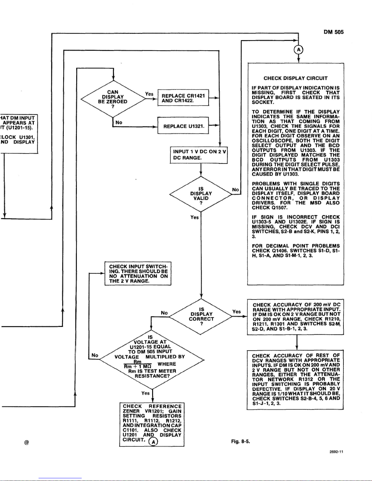
REPLACE
CR1421
,
AND
CR1422.
REPLACE
U1321.
-
4AT
DM
lNPUT
APPEARS
AT
IT
(U12O1-15).
LOCK
U13Q1,
MD
DISPLAY
t
-
INPUT
1
V
DC
ON
2
V
DC
RAHGE.
I
CHECK
INPUT
SWITCH-
ING.
THERESHOULD
BE
NO
ATTENUATION OM
THE
2
V
RANGE.
i
>f
Yes
r
RESISTANCE?
CHECK
REFERENCE
ZENER
vttima;
GAIN
SETTING
RESlSTORS
1
I
R1111,
Rftl2,
R1212,
AND INTEGRATlON
CAP
1
~1101.
ALSO
CHECK
U1201
AND
DISPLAY
CIRCUIT.
a
CHECK DISPLAY ClRCUlT
IF
PART
OF
DISPLAY lNDlCATlON IS
MISSIHG, FIRST CHECK
THAT
DlSPLAY
BOARD
IS SEATED IN
ITS
SOCKET.
TO
DETERMINE
IF
THE
DISPLAY
INDICATES
THE
SAME
INFORMA-
TION
AS
THAT
COMING
FROM
U1303,
CHECK
THE
SIGNALS
FOR
EACH DIGIT,
ONE
DIGIT
AT
A
TIME.
FOR
EACH
DIGIT
OBSERVE
ON
AN
DURlNG THE
DIGIT
SELECT
PULSE,
ANY
ERROR
tNf
HAT
DIGITMUSTBE
CAUSED
BY
U1303.
PROBLEMS
WITH SINGLE DIGITS
CAN USUALLY
BE
TRACED
TO
THE
I
DISPLAY ITSELF, DISPLAY
BOARD
CON'NECTOR,
OR
DISPLAY
DRIVERS.
FOR
THE
MSD
ALSO
CHECK
01507.
1F
SlGW IS INCORRECT
CHECK
Ui303-5
AND
U1302E. IF
SIGN
IS
MISSING,
CHECK
DCV
AND
DC1
SWITCHES,
S2-8
and
S2-K,
PINS 1,2,
3.
FOR
DECIMAL
POINT PROBLEMS
CHECK
Q1406. SWITCHES
M-D,
S1-
H,
SI-A,
AND
S1-M-1,
2,
3.
4
CHECK
ACCURACY
OF
206
mV
DC
RANGE WITH APPROPRIATE INPUT.
.
IF
'DM
IS
OK
ON
2
V
RANGE
BUT
NOT
ON
200
mV RANGE,
CHECK
R1210,
R1211.
a1301
AND
SWITCHES
S2-M,
S2-D,
AND
Sf-B-1-2,s.
L
I
--
CHECK
ACCURACY
OF
REST
OF
DCV
RAMGES WITH APPROPRIATE
INPUTS.
IF
DM
FS
QKON
200
mVAND
2
V
RANGE
BUT NOT
ON
OTHER
RANGES, EITHER
THE
ATTENUA-
TOR NETWORK R1312
OR
THE
INPUT SWITCHING
IS
PROBABLY
DEFECTIVE.
IF
DTSPLAY
ON
20
V
RANGE IS
1/10
WHATITSHOULO
BE,
CHECK
SWITCHES
S2-B-4,5,6 AND
S1-J-1,2,
3.
Page 66

DC
CURRENT
CHECK
POWER
SUPPLIES
K='
CHECK
DC
VOLTS
'=-+
CHECK
THAT
TEST
LEADS
ARE
CONHECTED
TO
LOW
AND
mA
FUSE
F1521
CHECK
FOR
A
DC
VOLTAGE
AT
ADC
INPUT
(U3201-15)
THAT
CORRESPONDS
TO
EXPECT
ED
'READING.
FULL
SCALE
INPUT
CURRENT
ON
AMY
DC
CURREMT
RANGE
SHOULD
PRODUCE
200
mV
DC
ATY1201-15.
I
VOLTAGE
AT
W1201-15
CORRECT
S2X4,
5,
6
rnwrCnL
i
CONVERTED
DC
CHECK
SWITCHES
VOLTAGE
(0.2
V
F.S.)
BETWEEN
CURRENT
PRESENT
AT
INTlFm
<
SHUNTS
AND ADC
SWITCH
S3-,
I
CHECK
CURRENT
SHUMTS
R1425,
R1426,
AND
R1521.
CHECK
INPUT SWITCHING
FDR
THE
SHUNTS.
ALSO
CHECK
PROTECT10N
BRIDGE DIODES
CR1621.
flg.
8-6.
Page 67

OHMS
CHECK
POWER
SUPPLIES
G
I
CHECK
DC
VOLTS
I
REPLACE
LAMP
DS1410.
ALSO
CHECK
CR1301
AND CR1302
FOR
GOOD?
LEAKAGE. THEY
MAY
HAVE
BEEN
DAMAGED
WHEN
LAMP
WAS
y
u
INPUT
SHORTED
IS
DISPLAY
E-i,
2,
3
ZERO
w
Yes
71
CONNECT A KNOWN
RESISTOR
TO
DM
INPUT
WHICH
IS
CLOSE
IN
VALUE
TO
FULL
SCALE.
MEASURE
VOLTAGE
FROM
VOLTSIR
TO
LO
INPUT.
FOR
FULL
SCALE
READING.
VOLTAGE
ACROSS
RESISTOR
BEING
MEASURED
SHOULD
BE
0.2 v FOR
200
n
RANGE;
0.2
v
FOR
LO
L-2
AND
REST
OF
RANGES
AND 2 V
FOR
HI
R
AND
REST
OF
RANGES.
NOTE
THAT
RESISTANCE
MEASURED
BY
DM
505
WlLL
BE
PARALLEL
COMBINAT
ION
OF
RESISTOR
AND
TEST
M'ETER
RESISTANCE.
t
CHECK
PATH
FROM
VOLTS/fi
INPUT
TO
ADC
INPUT
(U1201-15).
VOLTAGE
AT
THESE
POlNTS
SHOULD
BE
EQUAL.
WMEM
MEASURING
VOLTAGE
AT
U1201-15
THE
MEASUREMENT
DEVICE
READfNG
WlLL
BE
THE
UNLOADED
VOLTAGE
MULTIPLIED
..arr,
WHERE
Am
IS
MEASUREMENT
DEVICE
RESISTANCE.
MEASURE
VOLTAGE
FROM
U1311-2
TO
U1311-6.
IT
SHOULD
BE
10 V ON
200
fi
RANGE;
lOV
FOR
MIR
AND
REST
OF
RANGES;
AND
1
VFOR
PO
n
ANDREST
OF
RANGES.
CHECK
CURRENT
SOURCE
Q1311
AND
ASSOMATED
COMPO-
NENTS.
IF
THESE
ARE
OK,
CHECK
R1304,
R1413,
R1305.
ALSO
CHECK
U1311.
/
VOLTAGES
AT
U1311-2
AND
CHECK
OP
AMP
W311
AND
PROTECTION
DIODES
CRt301
AND
CR1302.
Fig
&7.
CHECK
kR
SWITCt
S2-F-1,2,3 ANQS2-F*
6;
ATTEFFUAT
SWLTCHES;
PRO71
TlON
DIODES
CR1
AND
CR1302;
Rlr
AND
W317.
Page 68
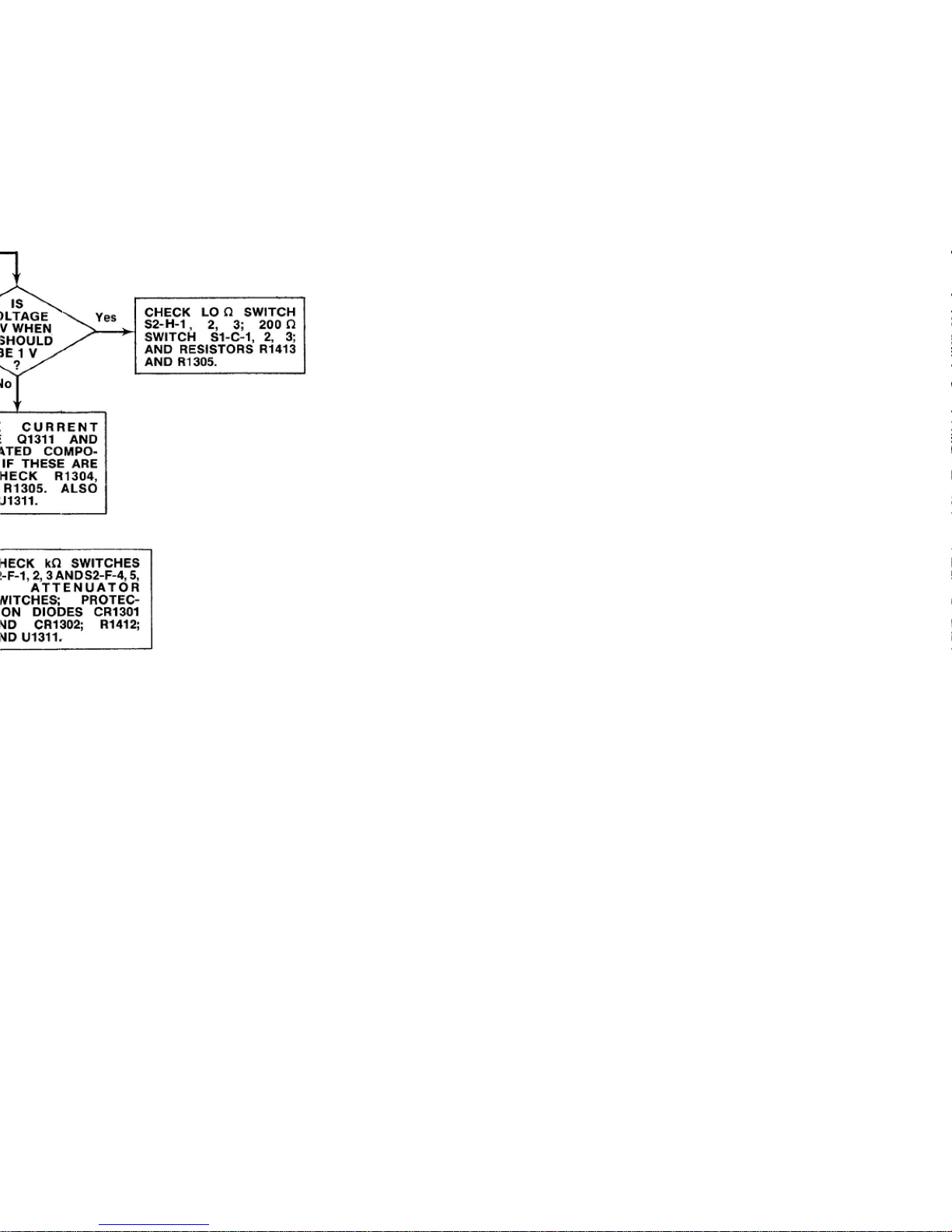
CHECK
LO
n
SWITCH
$2-H-1 , 2,
3;
200
R
SWITCH
S1-GI,
2,
3;
AND
RESISTORS R1413
AND
R1305.
HECK
R1304.
1
!-F-l,2,
3
AMDS2-F-45,
ATTENUATOR
WITCHES;
PROf
EC-
ON
DIODES
CR1301
VD
CR1302;
Rf412;
HD
U1311,
Page 69

AC
VOLTS
CHECK
POWER
SUPPUES,
MISCELLANEOUS NOTES
INABILITY
TO
ZERO
MAY
BE
CAUSED BY
LEAKY
U1211
IMWTS
OR
LEAKY
~1215.
IF
zEao
CAN
BE
SETON
200
mVAMD2 YRANGEBYT
ISOFFON20 VRANGEC1021(
86
1
MAY
BE
WRONG VALUE.
0
AN
ABNORMALLY
LOW
DISPLAY
IEEDICATTON
AT
20
kHz
OM
200
mV
AND 2 V
RANGE
CAN
BE
CAUSED
BY
U12f
l
BEING
DEFECTIVE.
AMPLITUDE
NONLINEARITY CAN
BE
CA~SED
BY
LEAKY
FEEDBACK
DIODES
CR1221
AND
CR1222.
WlTH
AC
VOLTAGE
AT
INPUT,
CHECK
FORADCVOLTAGEATAC
CONVERTER
OUTPUT.
ACROSS
~1221,
WHICH
CORRES~UDS~TO
THE
INPUT
VOLTAGE. FULL SCALE
INPUT
SHOULD
PRODUCE
2
V
DC
ACROSS
C1221
ON
ANY
ACV
RANGE. MEASUREMENT DEVICE
READING
WILL BE SLIGHTLY
LOWER
THAN EXPECTED
BECAUSE
OF
ITS LOADING
EFFECT.
VOLTAGE
ACROSS 61221
CORRECT
S2-C-4,s
CHECK
AC
VOLTAGE
AT
U1321-6.
AMPLlTUWE WlTH
FULL
SCALE
lfitPUT
SHOULD
BE
200
mV
ON
200
mV
AND
20
V
RANGES,
2
V
ON
2
V
AND
200 V RANGES
AND
500
mV
ON
500
Y
RANGE-VOLTAGEWILLBE
SLIGHTLY LESS BECAUSE
OF
NORMAL LOSSES BEFORE U132t.
t
I
CHECK
AC
CONVERTER
U1211
AND
ASSOCIATED
COMPONEMTS, IF
AT
U1321-6
SOME
RANGES
WORK
AND
OTHERS
CORRECT
DON'T,
CHECK
GA1N
SETTrNG
RESISTORS
AND
SWITCHES
BETWEEN U1321-6
AND
U1211-2.
I
CHECK
GAIN
OF
U1321.
AC
VOLTAGE
AT
U1321-3
AND
U1321-6
SHOULD
BE
EQUAL.
NOTE
THAT
I
MEASUREMENT
DEVICE
MAY
I
DECREASE
THE
YOLTAGE
AT
U1321-3
DUE
TO
CAPACITANCE
AND
RESISTANCE 50
THE
TWO
MEASUREMENTS SHOULD BE
MADE
$1
MULTANEOUSLY.
NO
L11321
EQUAL
ASSOCIATED
COMPONENTS
-
CHECK
INPUT
SWlTCHING
AND
ATf ENUATOR
COMPENSATION
CAPS
C1312, C1313,
AND
C1311.
WHEN
MAKING
MEASUREMENTS
AT
THE
ATTENUATOR
BE
AWARE
OF
THE
LOADING
EFFECT
OF
CAPACITANCE AMD RESISTANCE
OF
THE
MEASUREMENT DEVICE.
Page 70

STEP
1
I-15.75
V
R1021
ADJUSTMENT
LOCATIONS
STEP
6
Page 71
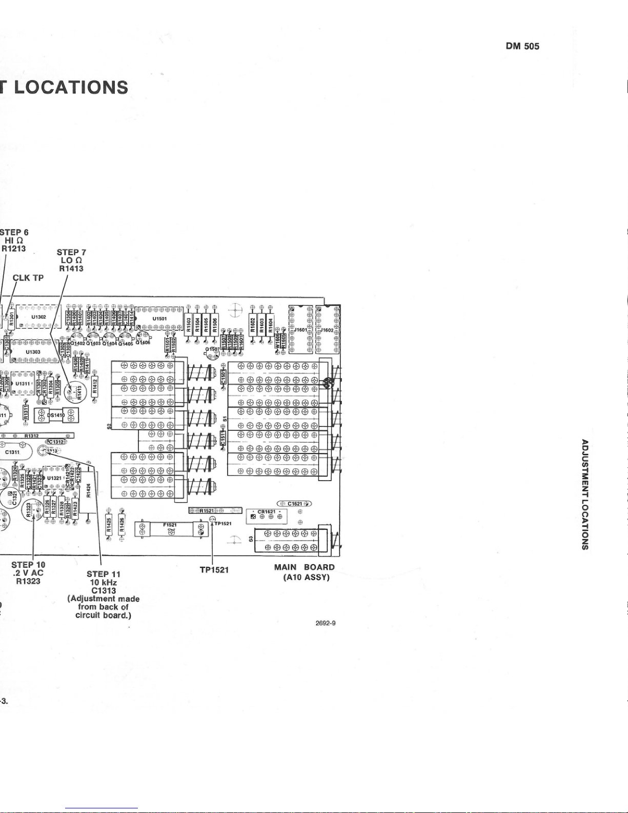
r
LOCATIONS
STEP
6
HI
R
. STEP?
I
LO
n
R1413
1
CLKTP
1
STEP
10
I
-2
Y
AC
Sf
EP
11
R1323
10
kHz
MAlN
BOARD
(A10
ASSY)
C13f
3
(Adjustment
made
from
back
of
circuit
board.)
Page 72

POWER
SUPPLIES
FOR
ANY
MALFUNCTION
WHEH
THE
CAUSE
IS
NOT
READILY
APPARENT,
FIRST
SUPPLIES.
f
12
V
SUPPLY
NO
ALSO
CHECK
FOR
EXCESSIVE
+5
Y SUPPLY
LOAD
ON
f 5 V
SUPPLY.
13A
AND
138
CHECK
FOR
MALFUNCTION
IN
-12 Y SUPPLY
WHICH
MAY
1
LOAD
DOWN
THE
/
TRANSFORMER.
I
ALL
SgEPLIES
I
Page 73
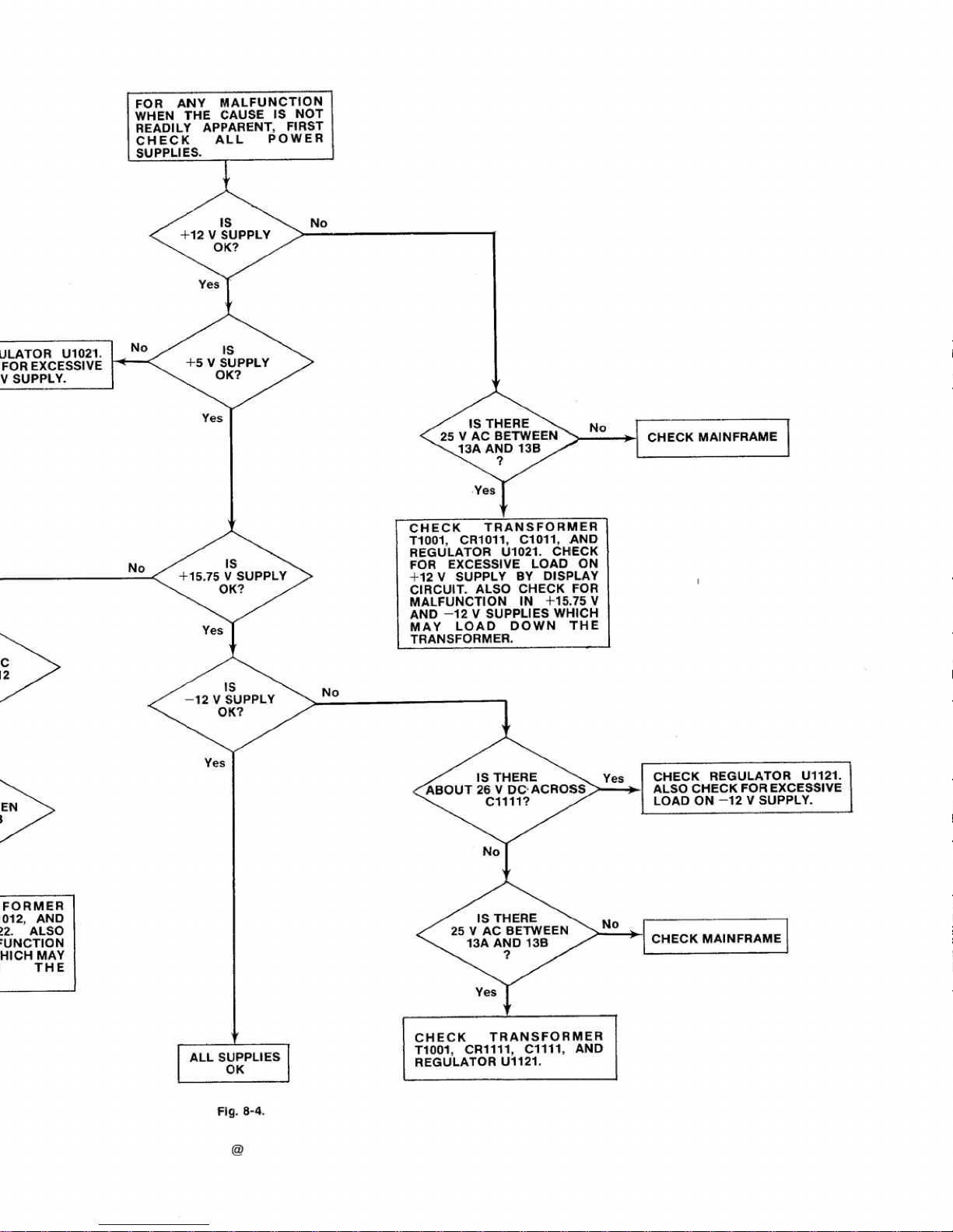
FOR
ANY
MALFUNCTION
WHEN
THE
CAUSE
IS
NOT
READlLY
APPARENT,
FIRST
SUPPLIES.
No
+12
v
SUPPLY
;
FOR
EXCESSIVE
+5
V
SUPPLY
v
SUPPLY.
Yes
22.
ALSO
FUNCTION
rHlCH
MAY
IS
THERE
CHECK
MAINFRAME
CHECK
TRANSFORMER
T1001,
CRlOlt. C1011,
AND
REGULATOR
U1021.
CHECK
FOR
EXCESSlVE
LOAD
ON
+12 Y SUPPLY
BY
DlSPLAT
CIRCUIT.
ALSO
CHECK
FOR
MALFUNCTION
IN
t15.75
V
AND -12
V
SUPPLIES
WHICH
MAY
LOAD
DOWN
THE
TRANSFORMER.
ALL
SUPPLIES
&
-12 v SUPPLY
NO
IS
THERE
R'
MAlMFnmE
1
Yes
CHECK
TRANSFORMER
T1001,
CR1111, C1111,
AND
REGULATOR U1121.
ALSO
CHECK
FOR
EXCESSIVE
Page 74

CHECK
POWER
SUPPLIES
AC
CURRENT
'7
CHECK
DC
VOLTS
'-4
CHECK
AC
VOLTS
Q
I
CHECK
DC
CURRENT
I
NOTE:
THE
DM
505
AC
CURRENT
READING
WILL
BE
SLIGHTLY
HIGHER
(4
TO 6 COUNTS)
FOR
FULL
SCALE
AT
HIGHER
FREQUENCIES
(1
k
TO
10
kHx).
THIS
tS
DUE
TO
VERY
LOW
SOURCE
IMPEDANCE
OF
CURRENT
SHUNTS,
WHICH IS
NOT
AFFECTED
BY
STRAY
CAPACi-
TANCE
TO
THE
SAME
EXTENT
AS
AC
VOLTAGES
FROM
THE
ATTEN-
UATOR NETWORK.
SZ-L-3
CORRECT
S2-k-1,
2,
3
CHECK
CURRENT
SHUNTS
R1425,
R1426,
AND
R1521
Page 75

PARTS
LOCATION
GRID
Fig.
8-10.
Main
Board
(AlO).
Page 76
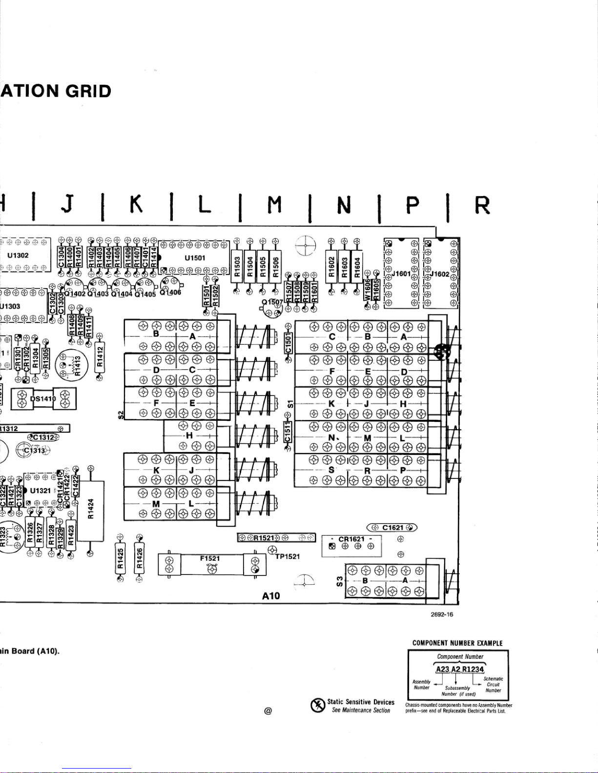
ATION
GRID
11n
Board
(AtO).
COMPOMENT
HUMBER
MJlHPLE
Component
Number
Page 77

Table
8-2
COMPONENT
REFERENCE CHART
Page 78

Page 79

i
+I
ZV
UNREG
I
-
P+SV
UMREC
NOTES
:
*
TOP
Vf
w
EW
+sv
1
S1
208rnV
52
OCV
INPUT
CONDITIDNINC
@
mae-21
MAIN
BOARD
Static
Sensitive
Devicts
See
Ma-
Shn
COMPONENT
MUYlBER
EXAMPLE
hwnenf
Nu&
V
.
--
I
C7aslsWUnM
ahmp~nemk
have
nr
AaJembly
thmh
~ehx-see
ewd
ol
Redma&
Uedncal
Pak
hd
Page 80

PARTS
LOCATION
GRID
Fig.
811.
Display
Board
(All).
Static Sensitive
Devices
See
Maintenance
&lion
COMPOHEllT
NUMBER
€%AMPLE
ComNnenf
number
-
I
A=W
J
I.
t
hut
Number
(d
und)
UlrarmpumM
mwnemk
no
Wmbly
Hunter
pel~x-e
end
ol
Replaceable Oenrlul
Pafa
LsI
Page 81
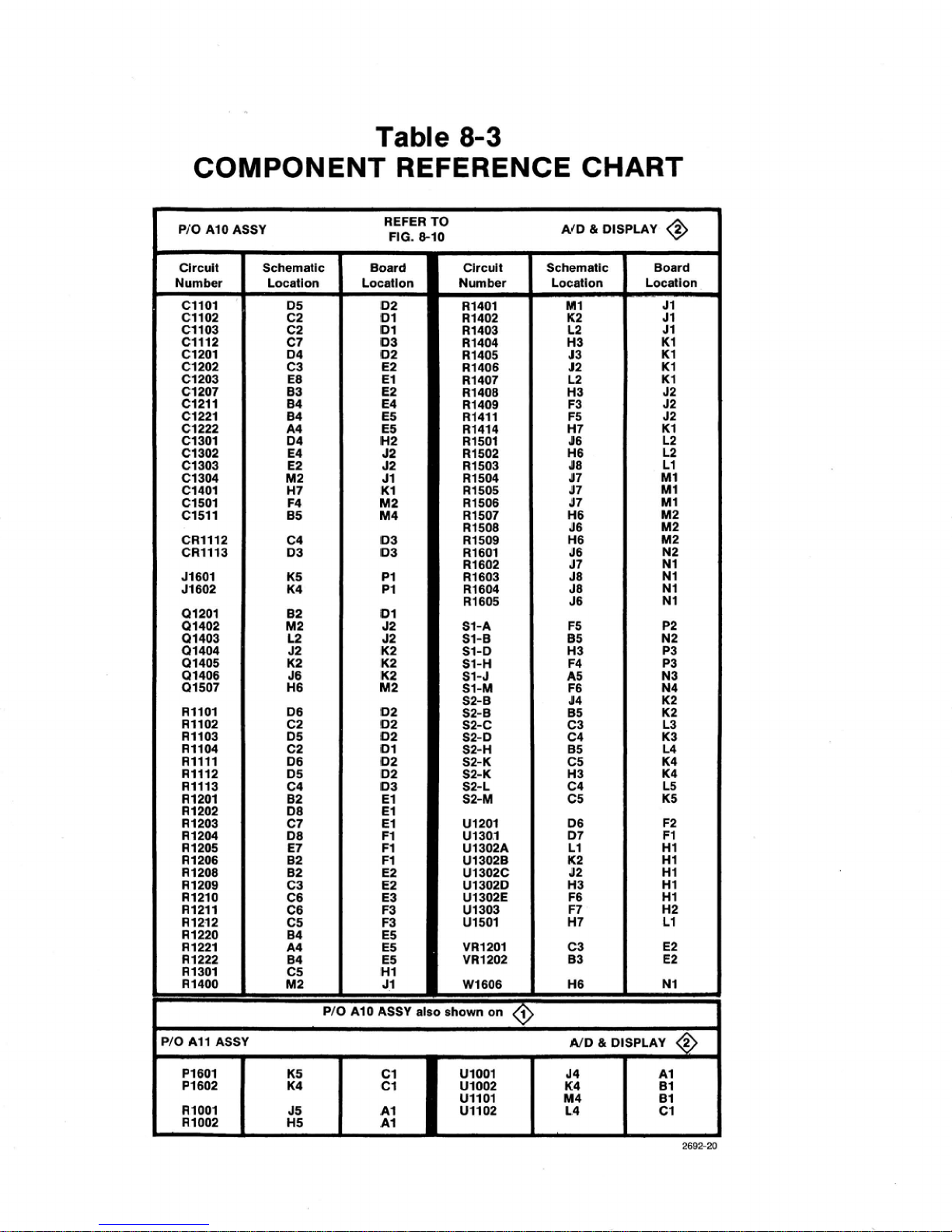
Table
8-3
COMPONENT
REFERENCE
CHART
Page 82
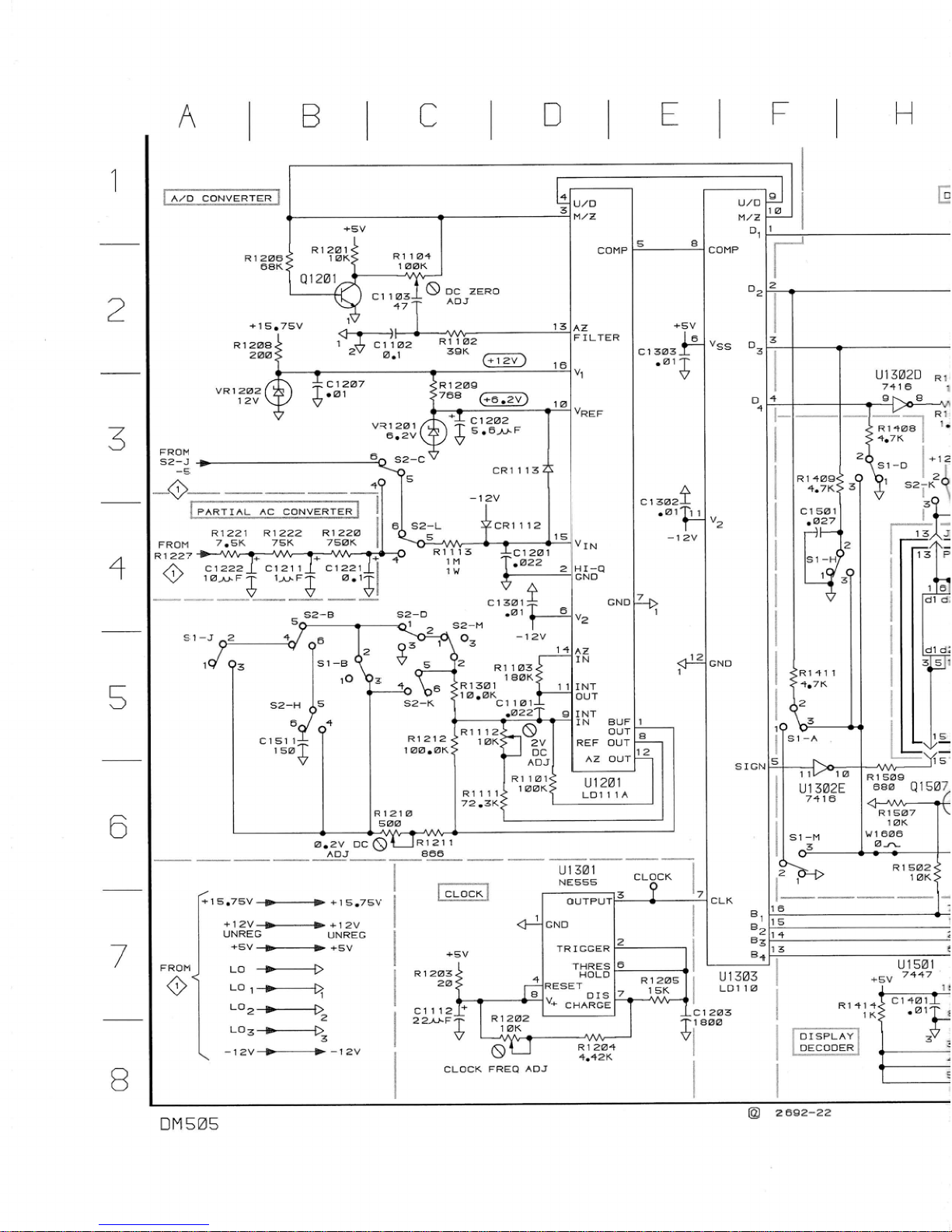
I
I
I
I
I I
A/D
CONVERTER
-@----
PARTIAL
AC CONVERTER
R1221
R1222
+12v-+12v
+sV
-
+5V
TR
1
GGER
LO
-
-12v-
-12v
CLOCK
FREQ
ADJ
@
26Q2-22
DM505
Page 83
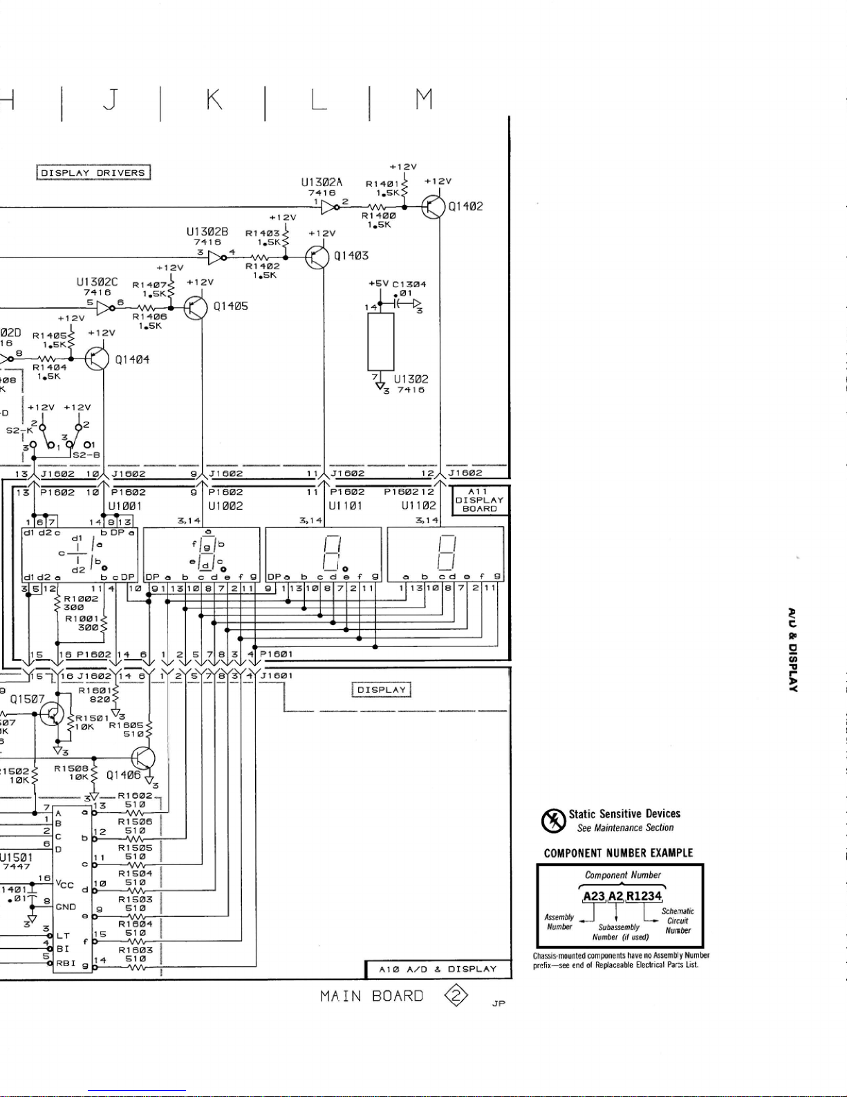
!DISPLAY
DRIVERS
1
Static
Sensitive
Devices
See
Maintenance
Section
COMPONEMT
NUMBER
EXAMPLE
Component
Number
I
Number
Subassemb!~
N~~M
Number
(11
medl
Cnass
rmunled
comwnems
hdw
m
Awmb
y
Nrmper
pref
x-tee
end
01
Replaceable
E
eclr
cal
Pact
L~sr.
MAIN
BOARD
@
,,
Page 84
REPLACEABLE
MECHANICAL
PARTS
PARTS
ORDERING
IMFORMATION
INDENTATION
SYSTEM
This
mechanical
parts
list
is
indented
to
indlcate
item
Replacement
parts
are available from
or
through your local
relationships. Following
is
an
example
of
the
indentation
system
Tektronix, Inc.
Field
Office
or
representative.
used
in
the
description column.
Changes
to
Tektronix instruments
are
sometimes made to
accommodate improved components
as
they become available,
and to give you the benefit of the latest circuit improvements
developed in
our
engineering department. It 1s therefore
important,
when
ordering
parts,
to
include
the
following
information in your order:
Part
number, instrument
type
or
number, serial number, and modification number
if
applicable.
If
a
part
you
have
ordered
has
been replaced with
a
new
or
improved
part,
your local Tektronix, Inc.
Field
Office
or
representative will
contact
you
concerning
any
change
in
part
number.
12345
Name
Description
Assembly
andlor
Component
Attaching
parts
for
Assembly
and/or
Component
---
-+-
Detail
Part
of
Assembly
andlor
Component
Attaching
parts
for
Detail
Part
---
-+-
Paris
of
Detail
Part
Attaching
parts
for
Parts
of
Detail
Part
,.--
=+*-
Change information, if
any,
is
located at the
rear
of
this
Attaching
Parts
always
appear In
the
same indentation
as
manual.
the
item a mounts, while
the
detail
parts
are
indented to
the
right.
Indented items
are
part
of,
and
included with,
the
next
higher
SPECIAL
NOTES
AND
SYMBOLS
indentation.
The
separation
symbol
-- - --
-
Indicates the
endof
attaching parts.
XOOO
Part
first
added
at
this serial number
OOX
Part
removed
after
this serial
number
FIGURE
AND
INDEX
NUMBERS
Items
in
th~s
section
are
referenced by fiqure
and
index
.
-
numbers to
the
illustrations.
n
ACTR
ADPTR
ALlGN
AL
ASSEM
ASSY
AnEN
AWG
80
BRKT
BRS
BRZ
BSHG
CAB
CAP
CER
cnAs
CKT
COMP
CONN
cov
CPCG
CRT
OEG
OWA
lNCH
NUMBER
SIZE
ACTUATOR
ADAmER
ALIGNMENT
ALUMINUM
ASSEMBLED
ASS€ MBLY
ATTENUATOR
AMEFtlCAN WlRE GAGE
BOARD
BRACKET
ERASS
BRONZE
BUSHING
CABINET
CAPACITOR
CERAMIC
CHASSIS
CIRCUIT
COMPOSTTION
CONNECTOR
COVER
COUPLING
CATHODE RAY
TUBE
DEGREE
DRAWEA
ELCTRN
ELEC
ECCTLT
ELEM
EPL
EQPT
EXT
FIL
FLEX
FLU
F
LTA
FR
FSTNR
FT
FXD
GSKT
HDL
HEX
HEX
HD
HEX
SOC
HLCPS
HLEXX
HV
IC
ID
IDEMT
IMPLR
Amchlng
pa*
must
be
purchased
separately,
unless
otherwh
specllkd.
ITEM
NAME
In the
Parts
List,
an
ltem
Name
is
separated
from
the
description by
a
colon
I:).
Because
of
space
limitations,
an
ltem
Name
may sometimes
appear
as
incomplete. For further ltem
Name
identification,
the
U.S.
Federal Cataloging
Handbook
H6-I
can
be
utilizd where
possible.
ABBREVIATIONS
ELECTRON
ELECTRICAL
ELECTROLYTIC
ELEME
Wr
ELECTR:CAL PARTS LIST
EQUIPMENT
EXTERN4L
FlLLlSTER
HEAD
FLEXlBLE
FLAT
HEAD
FILTER
FRAME
or
FRONT
FASTENEA
FOOT
FIXED
GASKET
HANDLE
HEXAGON
HEXAGONAL
HEAD
HEXAGONAL
SOCKET
HELICAL COMPRESSION
HELICAL EXTENSION
HIGH
VOLTAGE
INTEGRATED
ClRCUlT
INSIDE DIAMETER
lOENFlFlCATlON
IMPELLER
IN
lNCH
INCAND lMtAt4DESCENT
tNSUL IMSULATOR
INTL INTERNAL
LPHLDR LAMPHOLOER
MACH
MACHINE
MECH
MECHANICAL
MTG
MOUMTING
NIP
NIPPLE
NON
WlRE NOT WlRE
WWND
OBD
ORDER
BY
IJWCRlPTlON
OD
OUTSIDE DIAMETER
OVH
OVALHEAD
PH
BRZ
PHOSPHOR BRONZE
Pi
PLAlM
or
PLATE
PLSTC
PLASTIC
PN
PART
NUMBER
PNH
PAN
HEAD
PWU
POWER
RCPT
RECWTACLE
RES
RESISTOR
RGD
RIGID
RLF RELIEF
RTNR RETAlNER
SCH
SOCKETHEAD
SCOPE
OSCtLLOGCOPE
SCR
SCREW
SE
SINGLE
END
SECT
SECTION
SEMICOND SEMICOMOUCTOR
SHLO SHIELD
SHLDR SHOULDERED
SKT
SOCKET
SL SLIM
SLFCKG SELFIOCKING
SLVG SLEWING
SPR
SPRING
SQUARE
SQ
SST STAINLESS STEEL
STL
ST
EEL
SW
SWITCH
T
TUBE
TERM TERMINAL
THO
THREAD
THK THICK
TNSN TENSION
TPG
TAPPING
TFlH
TRUSS
HEAD
V
VOLTAGE
VAR VARIABLE
WI
WITH
WSHR
WASHER
XFMR
TRANSFORMER
XSTR
TRANSISTOR
Page 85
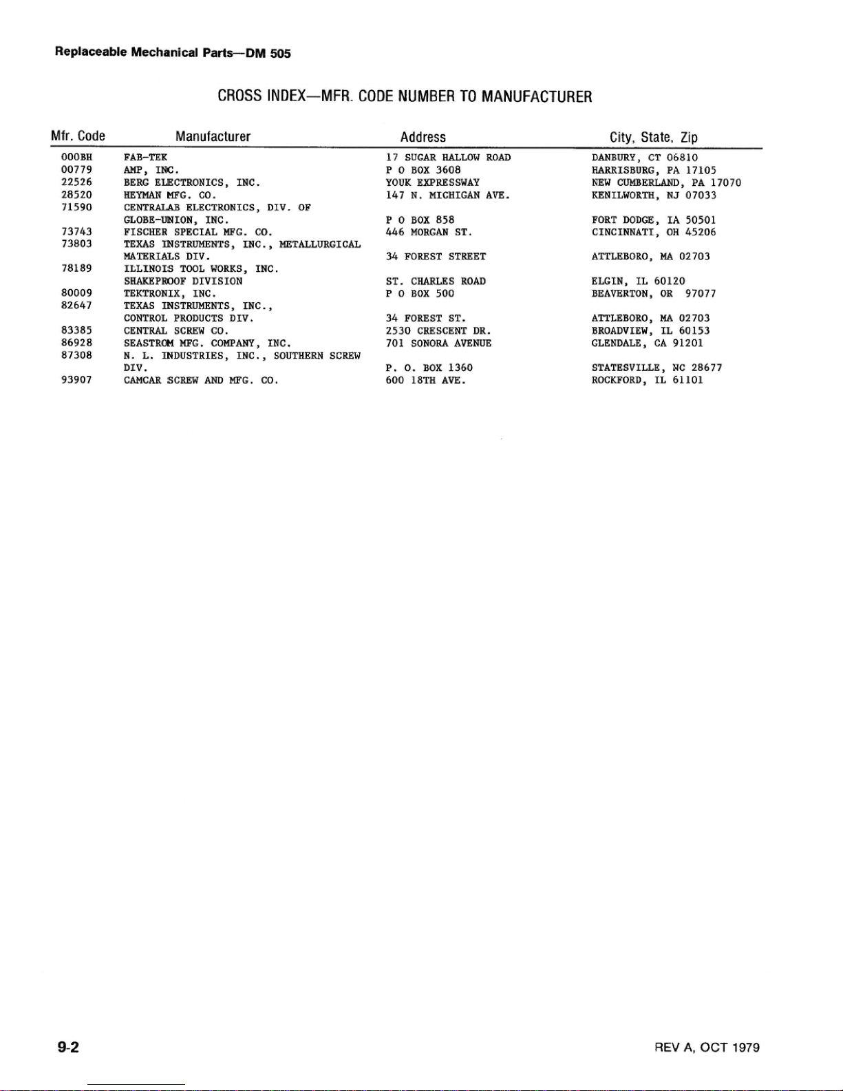
Replaceable
Mechanical
Parts-DM
5115
CROSS
INDEX-MFR.
CODE
NUMBER
TO MANUFACTURER
Mfr.
Code
Manufacturer
Address
City,
State,
Zip
OOOBli
FAB-TEK
17
SUGAR
HALLOW
ROAD DANBURY.
CT
06810
Am,
IHC.
BERG
BlECTROF1ICS,
WC.
HEW
WG.
CO.
CENTIlALda
ELECTROUICS,
DIV.
OF
GLOBE-WNXOH,
INC
.
PISCHER
SPECIAL
MFG.
GO.
TEXAS
TISTRUHENTS,
mC.,
METALLURGICAL
MATERIALS
DIV.
ILLINOIS
TQOL
WORKS,
fWC.
SNAKEPROOF
DIVISIOM
TEKTROHIX
,
INC
.
TEXAS
IMSTRUPIENTS,
me.,
CONTROL
PRODUCTS
D
IV
.
CENTRAL
SCREW
CO.
SEASTROM
PIFG.
COHPAHT,
IEIC.
N.
I..
TNDUSTRIES
,
ENC.
,
SOUTHERN
SCREW
DIV.
CAHCAR
SCREW
AND
MG.
CO.
P
0
BOX
3608
YOUK
EXPRESSWAY
147
W.
MICHIGAN
AVE.
P
0
BOX
858
446
MORGAN
ST.
34
FOREST
STREET
ST.
CHARLES
ROAD
P
0
BOX
500
34
WREST
ST.
2530
CRESCENT
DR.
701
SOMOKA
AVENUE
P.
0.
BOX
1360
600
18TR
AVE.
HABRISBWRG,
PA
17105
NEW
CU?BEIILIWD,
PA
17070
KENILWORTH,
NJ
07033
FORT
DODGE,
IA
50501
CIACIIWATT.,
OH
45206
ATTLEBORO
,
HA
02
703
BROADVIEW,
IL
60153
GLENDALE.
CA
91201
STATESVILLE,
HC
28677
ROCKFORD,
IL
61101
REV
A.
OCT
1979
Page 86

Replaceable
Mechanical
Parts--DM
505
Fig.
&
Index
No.
Tektronix
Part
No.
Seriallhlodel
No.
Eff
Dscont
Mfr
Code
Qtv
12345
Name
8
Descriation
Mfr
Part
Number
2
SHIELD,ELEC:
SIDE
1
MARKER,
1DEWT:MARKED
DM505
MULTIWTER
1
LRNS,LED
DSPL:RED
10
PUSH
BUTTON:GRAY
2
PUSH
BUTT0N:CBARCOAL
GRAY
1
JACK.TEP:BLUE
(ATTACHING
PARTS)
1
NUT,PLAXN,HEX.:0.25-32
X
0.375
IHCH
BUS
I
TERMINAL,LUG:0.25
INCH
DIA,SE
1
WASHER,FLAT:0.256
ID
X
0.438 INCU
OD,BRS
---*---
1
JACK,TIP:BLACR
1
JACK,
TIP
:
BLACK
(ATTACHING
PAWS)
1
WT,PLAXN,HEX.:0.25-52 X 0.375 INCH
BUS
1
TERMINAL,WG:0.25
INCH
DIA,SE
I
WASHER,FLAT:0.256
ID
X
0.438
INCH
OD,BRS
---*---
1
JACK,TIP:AED
1
JACK,TIP:RED
(ATTACHING
PARTS)
1 NUT,PMIN,HEX.:0.25-32
X
0.375
INCH
BRS
1
TeRMfNAL,GUG:0.25 INCH
DIA,SE
1
WASHER,FLAT:0.256
ID
X
0.438 INCH OD,BRS
---*---
1
NUT,PLAXN,RNUUL:0.25-28
X
0.25
INCH
L,BRS
I
STUD,SHOULDERED:6-32
X
0.40
INCH
tONG
1
KNO6,LATCR:
I
LATCH,RETAZNXUG:PLUG-XH
(ATTACHING
PARTS)
I
SCR,TPG,THD
FOR:2-32
X
0.312
fNCfl,PNH
STL
---*---
1
BAR,
LATCH RLSE
:
1
PANEL,FRONT:
(AITACHIAG
PARTS)
1
SCREW,MACHXNE:6-32
X
0.375
fNCH,TRH
STt
---*-*-
1
SUBPANEL,FRONT:
(A~ACHIW
PARTS)
2
SCR,TPG,THIl FOR:6-32
X
0.50
IWCH,PNH
STL
2
SCMW,TPG,TF:6-32 X 0.375,TAPTITE,PMH
---*---
1
CKT
BOARD
ASSY:DISFLAY(SEE All
EPL)
1 . TERM.
SET,PfN:36/0.025
SQ
PIW,ON
0.1
CTRS
1.
.
TERPI.
SET,PIN:l
X
36,O.l
CTR,O.9
L
2
SHIELD,ELEC:CIRCUIT
BOARD
(AITACHING
PARTS
1
SCREW,MACHINE:4-40
X
D.tB8
TMCB,PNH
STL
---*---
2
BRACKET,
SHIELD : POLYCARBONATF
6
EXTENSION
SHAPT:2.764 L
X
0.187
00
1
CUT
BOARD
ASSY:MAIN(SEE A113
EPL)
(ATTACHING
PARTS)
4
SCR,TPG,THD
POR:6-20
X
0.313
fNCH,PNH
STL
- - - * -
-,
-
.
CUT BOARD
ASSY
INCLIIDES:
1
.
HEATSINK,XSTR:AL W/0 TABS
1
.
SPAC&R,POST:O.
188"
HEX
1.627''
L,AL
2 . SOCKET,PLUG-IN:16
COMTACT,LOU
CLEARANCF:
1
.
SOCKET
,PLUG f N:MICROCIRCUfT,
8
CONTACT
1
.
CAPACfTOR:(SEE
A10C1313 EPL)
4
.
CLIP,ELECTRtCAL:FOR
0.25
INCH
DIA FUSE
2
.
BUTTON,PLUG:0.25
HTG
HOLEDIA,NYLON
1
.
SHIELD, ELEC:AC COMVERTER
1
,
SWTTCH,PUSM:(SEE
A10S2
EPL)
3095-402
A313-136
OBD
3095-402
A313-136
OBD
OBD
OBD
OED
OBD
OBD
OOOBH
80009
82647
7
3803
REV
A,
OCT
1979
Page 87
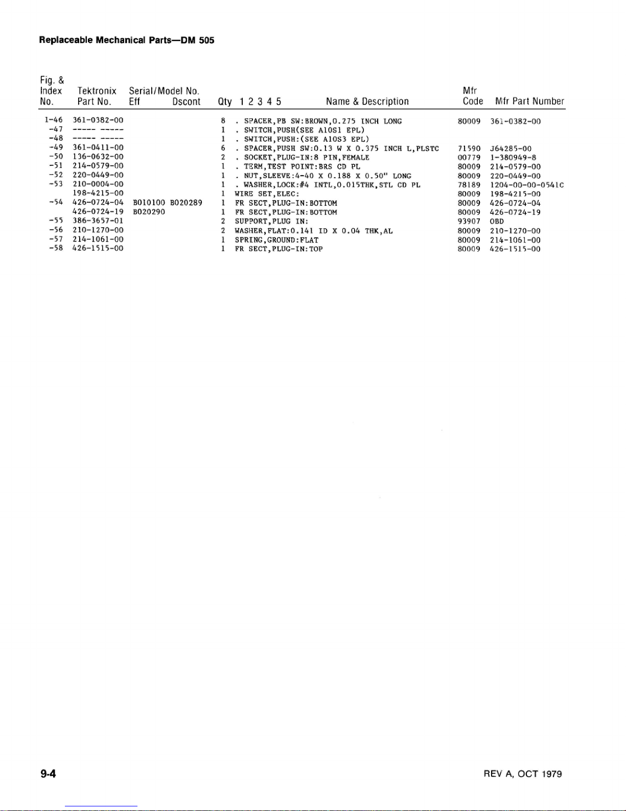
Replaceable
Mechanical
Parts--DM
505
Fig.
&
Index
Tektronix
SeriallModel
No.
Mfr
No.
Part
No.
Eff
Dscont
Qty
1
2
3
4
5
Name
&
Description
Code
Mfr
Part
Number
.
SPACER,FB
SW:
BROWN,
0.275
KMCH
LONG
.
SHfTCH,PUSH(SEE
AlOSl
EPt)
.
SFIIITCI~,PUSH:(SEE
~10~3
EPL~
.
S?ACER,PUSH
SW:0.13
W
X
0.375
INCH
L,FLSTC
.
SDCKET,PLUG-IN:8
PIN,FEMALE
.
TERM,TKST
P0INT:BRS
CD
PL
.
NUT,SLEEVE:4-40
X
n.188 X 0.50"
LONG
.
WASHEU,l.OCK:84
fNTL,O.O15THK,STL
CD
PL
WIRE
SET
,ELKC:
FR
SECT,
PLUG-I
H
:
BOTTOM
FR
SECT,PLUG-1N:BOTTOH
SUPPORT,
PLUG
f
N:
WASHER,FGAT:O.I41
ID
X
0.04
THK,AL
SPBtNG
,GROUND:
FLAT
FR
SECT,PLUG-IN:TOP
REV
A,
OCT
1979
Page 88

Page 89

Page 90

Fig.
&
Index
Tektronix
SeriallModel
No.
Mfr
No.
Part
No.
Eff
Dscont
Qty
1
2
3
4
5
Name
&
Description
Code
Mfr
Part
Number
Page 91

MANUAL
CHANGE INFORMATION
At
fektronix,
we
continully
&river
to
keep
up
with
the
latest
dmtronic
devehprnents
by
adding
circuit
and
~ornponent
irnpmvements
to
our
instruments
as
smn
as
thy
are
dwulopd
and
tested.
Ssmetimes,
due
to
printing
and
shipping
requirements,
WB
can't
get
these
changes
immediately
into
printed
manuale.
Hence,
your
manual
may
cmniak?
new
change
information
on
the
following
pages.
A
single
change
may
affect
several
sections.
Since
the
change
information
sheets
am
carried
in
the
manual
until
all
changes
are
prrnanently
antered,
some
duplication
my
aceur.
If
no
suuh
change
pagas
tappar
following
this
page,
your
manual
is
corm3
as
printed.
SERVICE
MOTE
Becausm
of
the
universal
parts
procurement
problem, -me electrical
parts
in
your
instrument
may
be
different
from
tha
dgscrihd in
the
Replaceable
Electrical
k-ts
List.
The
parts
used
will
in
no
way
alter
or
compromise
the
performance
or
mliability
of
thii
instrument.
They
are
Installed
when
necessary
to
ensure
prnrnpt
delivery
to
the
customer.
Qrdlw
mplawrnent
parts
from
the
Replaceable
El&al
Parts
List.
-
m
-
-
L.
*-bn
.r
Page 92
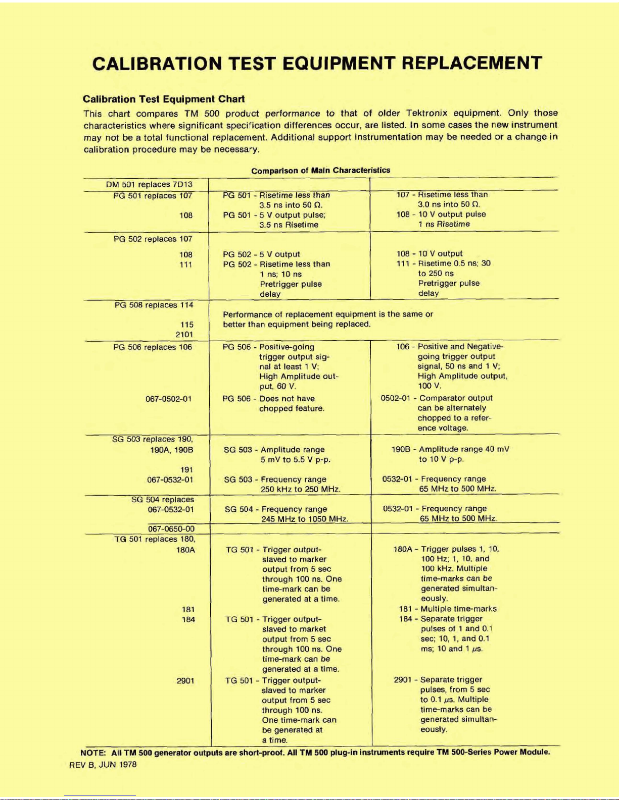
CALlBRATlON
TEST
EQUIPMENT
REPLACEMENT
CatlbrMon
Ted
Equipment
Chad
-
This
6.R
cornparer
TM
500
proU
perf-in&
f&
hhi
k
daw
?&LM%$
equ~pfTi&:
Only
tho-
eharacteristlcei
where
significant
spec14Kiation
differences
occur,
am
listed.
In
ssms
mms
the
new
imrurnent
may
not
be
a
total
functional
raplament.
Additlond
suppM
inktrurnentation
may
Be
needed
or a chan*
in
calibration
procedure
may k necessary.
DM
501
repl~e~7[319
PG
501
raptaces
107
P'G
501
-
Rlsrrtlmr
1-8
than
107
-
Rislirnr
ks
than
J-Cu
-7
-
f
I
3,6
ns
into
50
n.
3.0
ns
into
50
R,
1
108
$G
a1
-
5 v output pulss;
108
-
10
\I
output
pulse
Sd
n~
RiWm
1
ns
Rlmtlrne
---
-.
5
-
PG
502
rwlaces
107
-
*.
-
--
- --
-A
-
1M
W
502-5V
output
108
-
10
V
autiut
111
PG
502
-
Rwirno
Iws
than
11
1
-
Rlwlme
0.6
ms:
3t3
t
ns;
IQ
ns
I(
to
250
M
Pretrigger
pulw
Prertlg~per
pulse
I
Performance
of
placement
equiprnmt
is
the
same
or
115
Mter
than
equipment
bdng replaced.
PG
506
-el
tiva-gol
qj
106
-
Pasltlve
and
Negatiw
frlugQr
output
sig-
going
triggar
output
n&
rwt
leaqt 1 V;
signal,
50
m
and
1
V;
High
Amplitude
out-
High
Amplituth
output,
put,
m
v.
100
v.
BG
Xt&
-
Dm
nd
have
.
0502-01
-
Camparator
output
chapped
feature.
can
be
alwnately
chopm
to a
refer-
etlce
voltago.
SG
603
-
Amplitude
ran*
5
mV
to
9.5
V
p-p.
l#B
-
AmplItti#~ range
40
mV
to
tov
p-p.
SG
603
-
Frequency range
a50
kHz
to
~FQ
MHz
TG
a1
-
Trigger
outprrt-
slaved
to
marker
output
from
5
SEC
thtough
100
ns.
One
time-mark
can
b
gerneratd
at
a
timw
0532-01
-
Fmque~ay
range
&5MHata5OOt#z.
SG
504
-
Frequerrcy range
24.5
MHz
to
IDSO
MHz.
TG
31
-
Rlgm
CutpiA*
duve~
te
markel
output
from
5
mc
through
100
ns.
Om
ttmmztrirk
mn
bo
mated
at
a
time.
TG
501
-
Trigger
output-
slaved
to
masker
output
fmm
5
thrwgh
1M)
ns,
One
time-mark
can
be
-retest
at
0532-01-
Frquency
ran-
65
MH2
to
500
MHz.
IlOA
-
Trigw
pulses
1,14
100
Hz;
1,10.
and
100
kHz.
Multiple
timemarks
an
he
**rate4
sirnultaw
eeusl
y
.
181
-
Multlple
tlinE-rtlark~
184 - Sapwata
triww
pulses
at
1
atnd
0.1
I=
10,
1,
md
0.1
Ins;
10
ad 1 #.
-1 - Separate
triggw
pui-,
from
5
%ec:
to
0.1
pa.
Multipre
timgmarb
can
be
gnertrtsd
dmultan-
mdy.
1
a
time.
I
NQTE:
All
TM
LW
gemrdor
rutplss
are
m-pr&.
All
TM
5W
plug&
instruments
rmqulrr
TM
WKtSaStes
Powr
Medcde.
REV
8,
JUN
1Q78
Page 93
Change
Reference:
TEXT
CORRECTIONS
Step
5.
parts
d.
and
e.
CHANGE
TO
READ:
d.
Set
the
ac
calibrator
for
0.224
Vac
ms
at
50
Hz
50.2
Hz
or
60
Hz
?0.2
Hz.
e.
CHECK--that
the
maximum
display
reading
is
51.0.
 Loading...