

Page 1

DlOl A
Digital Input/Output Module
The DIOlA Digital Input Output Module provides 32
digital input or output channels at TTL levels. These
channels are grouped into four &bit ports which can be
individually programmed for input or output by software commands. The inputs are read directly by the host
computer, and the outputs are latched. A power on reset
circuit automatically configures all ports as inputs when
the DIOlA module is powered up.
I/O connections are made to on-card quick disconnect
screw terminal blocks, which accept 16-24 gauge wire
stripped 3/W. In addition to the screw terminals, a
mass termination connector for ribbon cable is provided
on the forward edge of the module.
CAUTION
Always turn off the data acquisition system
power supply before installing or removing
modules. To avoid the possibility of EMI radiation, never operate the system with the
top cover open or removed.
module, and is functionally compatible with the older
module. The older DIOl module has hardware switches
for port configuration, while this function is performed
through software for the DIOlA.
User Connections
User connections can be made to either the quick disconnect terminal blocks at the top of the module, or to the
mass termination connector located at one end of the
board <through the supplied ribbon cable).
Table 1. User-configured Components
Component
Screw Terminals
I/O Connector
t
Designation
Jl-J14
J6
Function
Input/Output
connections
Quick Disconnect
Mass Termination
for Ribbon Cable
The DIOlA module can be installed in any available slot
in any Keithley/DAC Data Acquisition System. However, for best performance any analog modules should
be plugged into the lowest-numbered available slots,
leaving the higher slots for digital modules. To install the
module in a Model 500 or Model 556, remove the top
cover and insert the module in any available slot with the
component side of the module facing the power supply.
To install the module in a Model570 or a Model 575, open
the clamshell cover and insert the module into the option
slot with the component side of the module facing up.
See your data acquisition system manual for details on
opening the system and installing modules.
The DIOlA module can be identified by a Model 575,
5OOA, 5OOP, or 556 mainframe through the use of a Self-ID
resistor which is mounted on the module. The value of
this resistor is measured by the mainframe, and an JD
code is generated from the value. The DIOlA module
uses the same ID code 52 (4530 ohms) as the older DIOl
Documen~umbert 501-916-01 Rev. B
Copyright’ 1989 Keithky Instruments, Inc., Cleveland, OH 44139 (216)248-0400
Screw terminals for making input/output connections
are located on Jl, J2, J3, and J4 across the top edge of the
module board. The channelnumbers (0 to31) are marked
across the top edge of the board and are also shown in
Figure 1.
Two connections each for the module ground (GND) and
+5
volts (+5) are also included on the top edge of the
board. The terminals are intended to be used with 16 to
24
gauge wire stripped 3/W’, and the terminal blocks
can be pulled off of the strip to facilitate connections. A
typical input/output connection for the screw terminals
is shown in Figure 2.
In situations requiring rapid connection and disconnec-
tion of signal lines, J6 can be used as an alternate means of
signal connection. Figure 3 shows the pin diagram for J6,
which is designed for use with a matching optional rib-
DIOl A-l
Page 2

DIOIA
.Digital Input/Output Module
Mass Termination (J6) Screw Terminals (Jl J4)
I/
/
t
:
:
:
:
:
:
:
:
:
:
1
J6
Terminal Designations
Ground : Pins 1,36
+5 Volts :
PortA :
PortB :
PortC :
PortD :
Figure 1. DIOl AModule Configurafion
Pins 2,35
Pins3-10
Pins11 -18
Pins19-26
Pins 27 - 34
A
Strain Relief
-6 ’
\
Digital Device
p+
::
::
::
. .
::
::
::
::
::
. .
::
ir
CAUTION : Non-isolated lTL
Figure 2. Typical DIOl A Input Connecf ions
Connections only
bon cable available from Keithley. When connecting signals in this manner, the screw terminals should not be
used.
If FMI radiation becomes a problem, use shielded cables
for input and output connections. Connect the shield of
the cable to the baseboard ground ONLY (or one of the
GND terminals of the screw terminal connectors), and
leave the other end of the shield unconnected. Do not use
the shield of the cable as a signal carrying connection.
CAUTION
DIOlA inputs arid outputs are non-isoIated,
meaning that the circuit ground is connected
to power ground. Any circuits connected to
the module must also be referenced to power
ground and must not be floating, or themodule may be damaged.
DIOl A-2
Page 3

Pin 40
G:D CZ31
Ci30 c:29
Ci26 C:27
C:26 CZ25
C:24 0 i5v
Pin 39
Digital Input/Output Module
DIOlA
Input/Output Programming
The 32 digital I/O channels of the DIOlA are grouped
into four ports of 8 channels each. Port A consists of channels 0 to 7, Port B of channels 8 to 15, Port C of channels 16
to 23, and Port D of channels 24 to 31. The function of
each port (and thus, the 8 channels associated with that
port,) can be programmed individually for input or output through the use of software commands discussed below. The data written to or read from any port can be
handled as a byte of information, in which eight channels
are accessed at one time.
G:D C:23
CL A21
CZO CL9
Left edge
of Module
pin* I PinI
CL8 cE17
C&6
G:D
C&4 C&3
Ck2 &I
C&O
Ci6
GiiD c:7
C:6 CZ5
CZ4
Ci2 c&
0
+5v
c&
ci9
0
+5v
CZ3
Matching 3M Ribbon
Connector Part
No. 3417
TTL Levels and Loading Considerations
When configured for input, each channel of the DIOlA
represents one LS TT’L load to the external circuitry
(2Oj,tA high, 0.4mA low). Logic low should be between 0
volts and 0.5 volts, and logic high should be between 2
volts and 5 volts (standard TTL levels).
When configured as outputs, each channel is capable of
driving a maximum of 60 LS TI’L loads or 15 standard
TTL loads
(maximum
output is 1.2 mA high and 24 mA
low). Logic low will be in the range of 0 volts to 0.5 volts,
and logic high will be between 2.7 volts and 5 volts.
Commands
The DIOlA uses the slot dependent CMDA and CMDB
lines for setup and read/write operations. To select a
port for a read or write operation, or to configure the
ports for input or output, write to CMDA of the appropriate slot. In order to write or read data, write to or read
from CMDB for the appropriate slot. See Table 2 for a list
of the slots and memory locations corresponding to the
CMDA and CMDB lines. Figure 4 includes details on the
DIOlA register usage. Memory locations indicated for
these commands assume that the interface card in the
host PC is set for a base address of CPF80. Any other setting of the base address will require the appropriate offset of the supplied command locations.
Figure 3. Connecfor 16 Terminal Configurafion
DIOlA-3
Page 4

DIOZA
Channels
Digiid
input/Output Module
Select
Gonfigure
and
Port
Reg
setup
CMDA
(Write)
1
32
Input/Output
)
ReadMite Data
CMDB -
(Read/Write)
CMDA (write) Address - Select port, configure port
Must be issued in order to read or write data to a specified port.
b7 c
CMDB (read) Address - Digital input
Read data from specifkl port provided port is contigured as an input port.
CMDB (write) Address - Digital Output
Write data to specSed port provided port is configured as an ougxn port.
D5 D4 D3 D2 Dl DO
‘L
Beleot Port: O-Port 4 Ch O-7
Configure Port A: 1 -Output, O-Input
Contigure Port B : 1 -Output, 0 - Input
Configure Port C : I- Cutput, 0 - Input
Configure Port D: i-Output, O-Input
Enable Configuration Bits : 0 - Cff , 1 -On
1 -Port B. Ch 8-15
O-Port C, Ch16-23
3-Port D, Ch 24-31
Figure 4.
DIOlA-4
DIOIA Block Diagram and Command Register
Page 5

Digital Input/Output Module
DIOlA
Table2. Locations for Slot Dependent
Commands
Select/Configure
Slot
1
2
Port (CMDA)
XXX80
XXX82
xxx84 XXX85
:
5
6
7
8
9
10
xXx=1
xxx86
xxx88 XXX89
xxx8A
XXX8C
XXX8E
xxx90 x>o(91
xxx92 xxx93
;t 3 digits of IEUN addn
SELECT/CONFIGURE PORT
Location: Slot dependent CMDA write
The CODA write command is used to configure the ports
for input or output, and to select the port that data is to be
written to or read from. Refer to Figure 4 for the following discussion of the CMDA write data byte.
Digital I/O
OADB)
XXX81
XXX83
XXX87
xxx8B
xxx8D
xxx8F
s,
e.g.
“CFF
operations
NOTE
Upon power up, a random port will be selected; therefore, port selection should be accomplished prior to read or write operation
with CIvlDB.
NOTE
In
some
applications, you may find it useful
to read back the levels previously programmed to a DIOlA port configured for output. The value read back will be the last byte
value successfully programmed to the port.
This feature can be implemented using
BASIC’s PEEK command, or the equivalent
memory read function of other languages.
This WAS NOT a capability of the older DIOl
module, and should not be attempted using
the older module.
DIGITAL INPUT/OUTPUT operations
Location: Slot-dependent CMDB read or write
A CMDB read is used to access data from a selected port
when that port is configured as an input port. A CMDB
write is used to write data to the selected port when that
port is configured as an output port. Note that each of the
four ports can be individually programmed as either an
input or output port, as discussed above.
Bits D3 through D7 are used to configure the ports for input or output. Bit D7must be set to a logic 1 to enable bits
D3 through D6 to set their appropriate port to an input or
an output port. When bit D7 is set to a logic 0, bits D3
through D6 are ignored. Bits D3 through D6 are used for
PORT A through PORT D, respectively. Setting the appropriate bit to a logic 1 sets that port and
all associated
channels, to a digital output. Setting the appropriate bit
to a
logic 0
sets that
port, and
all associated channels, to a
digital input.
NOTE
Upon power up, all ports are set to be digital
inputs.
Bits DO and Dl are used to select a particular port for input or output. A value from 0 to 3 will select port A
through port D respectively. Port selection will always
occur with a CMDA write to the DIOlA module, regardless of the logic value of bit D7.
When a port is configured as an input port, the CMDB
command location is read to access the status of the channels associated with the port. Reading this location will
return an 8 bit binary number, with the DO thru D7 lines
representing the input lines for the selected port as indicated in Table 3. Since the inputs are not latched, the data
will reflect the condition of the input channels at the instant that the read operation is performed. Note that the
channels being read will depend on the port selected
with the CMDA write command discussed above.
If you need to know the status of a particular channel, a
logical AND instruction can be used to “mask oft?’ the unnecessary bit positions. The mask should contain zeros in
the irrelevant bit positions and logic ones in the bit positions representing the channels in question. The result of
ANDingthemaskwiththeinputdatawillthenbean8bit
binary number with each bit in an irrelevant position
equal to zero. The relevant channels will contain a 1 or a 0
depending on the status of the corresponding bit in the
masked byte (a 1 if the object bit is high, a 0 if the object bit
is low).
DIOlA-5
Page 6

DIOZA
Dig&z2 Input/Output Module
When reading a DIOlA port with the BASIC PEEK command, the returned value will be a decimal number be-
tween 0 and 255, depending on the status of the input
channels. The status of a particular channel can be determined by ANDing the returned value with the decimal
weighting for that particular channel.
sult is nonkero, the channel is high (logic 1).
EXAMPLE
telmlin~
100 POKE CMDA,O
110 STATUS6 = PEEK(CMDB) AND 64
If the value returned in variable STATUS6 is non-zero,
then channel 6 is high.
If a DIOl A port is configured as output, the value written
to CMDB should be the equivalent of an 8 bit binarynum-
ber, with the status of the 8 bits (1 or 0) representing the
status of the 8 channels of the selected port (high or low).
The channels affected will depend on the selected port, as
outied hi ‘I’abie 3.
into the outputs and will remain unchanged until the
port is written to again, or the port is configured as an input port.
the POKE command will be a decimal value in the range
from 0 to 255.
To change the status of one output channel while leaving
the others unchanged, you must know the status of all of
the channels. To accomplish this, a variable in the controiiing program could be assigned to the current status
of the port in question (and updated every time the port is
written to), or the output on the port could be read di-
The status of channel 6 on port A is to be de-
- Data wr&en to a port will be
From BASIC, the value written to the port using
If the ANDed re-
iatched
rectly from the port using the readback feature (and
stored in a variable).
channels on the particular port is known, the value of the
variable can be changed to correspond to the desired
status of the selected port, and this new value written to
the CMDB location.
In assembly language, this modification can be performed by using logical AND and logical OR instructions. When turning a single channel on (high) the vari-
able representing the current port status should should
be ORed with a number equivalent to an 8 bit binary
value with zeros in the bit positions to remain unchanged
and ones in the bit positions to be turned on. When turning a channel off, the port status variable should be
ANDed with an 8 bit binary value with ones in the bit positions to remain unchanged and zeros in the positions to
be turned off
From BASIC, the decimal weight of the bit to be turned on
or off should be added to (off to on) or subtracted from
(on to off) the decimal number that represents the current
er.d- r+-k.r
y”Lr 3LaLUJ. I‘“I GvuAyAc, I.” LULLI uLcul.LLtzL tt vu, IL W”l.uU
be necessary to subtract 8 from the decimal value representing the port status. To turn on channel 8, it would be
necessary to add 128 to the status.
It should be noted that the DIOlA module is command
compatible with the older DIOl module, with the added
programmability of the port configuration versus the
switch selectability of the older module. Programs written for the older module can be modified for use with the
new module by simply issuing a CMDA WRlTE to configure the ports before any input or output is accomplished.
Cr.” rwrm,rle Lrr Lr.... #.a.,.......-1 A -CL :r-..#...lA
When the current status of all the
DIOlA-6
Table 3.
Bit Position
Weighting
Port A ChanNos. 7 6
Port B Chan Nos. 15 14
Port CChanNos. 23 22
Port D Chan Nos.
Digital I/O Channels and Bit Values
1 D7 1 D6
128 64
31 30
D5 D4
32 16
5 4
13 12
21 20
29 28
I
D2
D3
8 4
3 2
11
10
19 18
27
26
Page 7

Digital Input/Output Module
DIOlA
Theory of Operation
A schematic drawing of the DIOlA module is located on
drawing number 501-206.
The DIOlA circuitry may be divided into six sections:
data bus buffering circuitry, port selection circuitry, port
configuration circuitry, channel input buffers, channel
output latches, and power up reset circuitry.
Data from the baseboard bus circuitry is applied to the
octal bus transceiver U13 (74LS245). Bus transmission direction of U13 is controlled by the baseboard Read/Write
line, while the CMDB line is used to enable the device
when reading or writing data to one of the 4 ports on the
module using the DIGITAL I/O command.
The two least significant bits of the data bus (DO and Dl)
are also applied to the port selection circuitry made up of
a dual D type flip flop U2 (74LS75) and a 3 to 8 line decoder U4 (74LS138).
select port mode, the values on the DO, Dl, and Read/
Write lines are latched into U4. When the CMDB line
next goes low, U4 decodes the input from U2 into an enabling signal to go to only 1 of the 4 ports (either the input
buffer or the output latch, depending upon the state of
the Read/Write line). For example, if 11 (binary) were
present at DO and Dl, and the Read/ Write line was active
(low), executing a CMDA write would latch the data into
U4; then the Y7 output of U4 would go low with the next
CMDB write, latching the data present on the bus at’that
time to the output of the port.
When a CMDA write is issued in the
Input/Output selection is performed by triple 3 input
nor gate Ul(74LS27) and quad latch U3 (74LS175). When
a CMDA write is issued (bit D7 high) the data on lines D3
to D6 is latched into the inverting outputs of U3. A low to
the output control of the output latches US, US, UlO, and
U12 (74LS374) allows the Read/Write line to clock the
data from the bus to the port. When D3 to D6 are low, the
output latches t&state and the select port registers of U4
enable the input buffer for the selected port.
The Self-ID resistor (R40) connected between pins 4 and
41 of the card edge connector allow the mainframe to
identify the module by reading the value of the resistor
with an A/D conversion circuit and generating a code
based on the value of the resistor. The ID resistor has a
value of 4.53 kilohms, with a tolerance of 0.1%.
The power up reset circuitry is used to ensure that all outputs power up in a high impedance state by holding the
clear line of U3 low until power up is complete, forcing all
inverting outputs of the quad latch high.
Troubleshooting Information
Troubleshoot the DIOlA by using the procedure out-
lined in Table 4. This process is fairly straightforward, as
signal tracing is simply a matter of checking for the correct digital logic level throughout the module.
If a defective part is found, a replacement can be ordered
from Keithley Data Acquisition and Control. Refer to the
Service Section of the hardware manual for ordering details. Part numbers for the module are located on the
component layout drawing (501-200).
DIOlA-7
Page 8

DIOIA
Digital
Input/Output Module
Table 4. DIOlA Troubleshooting Information
Step
1
I\Tote: Slot 10 locations
Component Required Condition Remarks
1
DIOlA module
2
channel O-31
3
computer
4
computer
5
ports B-D
channel O-31
6
7
computer
computer
8
9
ports ED
10
computer
11
computer
channelO-7
12
13
ports B-D
14
computer
15
computer
channelO-7
:;
ports ED
Install in slot 10
apply logic high (+Rr)
program ah ports as inputs and select port A
read back 255 from port A
repeat steps 4 and 5
apply logic low (WI
select port A
read back 0 from port A
repeat steps 8 and 9
program all ports as outputs and select port A
write 255 to port
all outputs high
repeat steps 13 and 14
select port A
write 0 to port
all outputs low
repeat steps 17 and 18
CMDAXXX92
CMDBXXX93
DlOl A Specifications
Channels: 32, software programmable in groups of 8 for
input or output
turn power on
apply to inputs
use CMDA write DATA 11111X00
use CMDB read
to test ports ED
apply to inputs
use CMDA write
use CMDB read
to test ports ED
use CMDA write
DATA 10000X00
use CMDB write
use logic probe/DMM
to test ports B-D
use CMDA write
use CMDB write
use logic probe/DMM to test ports B-D
General: AII inputs and outputs referenced to system
ground
AU inputs and outputs power up in high impedance state
as inputs for safety
Signal connection: Quick disconnect screw terminal
blocks, 40 pin receptacle for ribbon cable assembly
Input characteristics:
T&-compatible, high-true
High-level Input Current: 2OpA
Low-level Input Current: -0.4mA
Output characteristics:
TI’L-compatible, high true
Drive capacity: 60 IS-TIT, loads or 15 standard ‘ITL
loads; 24mA sink at 0.5V
Self-ID: resistor value - 4.53kQ zt.1 %. ID code 52
DIOlA-8
Accessories: Ribbon cable assembly, 6 foot, 40 conductor; one end mates with 40 pin receptacle on DIOIA,
other end is unterminated. KeithIey part number
5OO-cA3.
Cable ribbon plug, only - 3M part number 3417.
Parts List
The following components are used in the DIOlA module. Spares can be ordered from the repair department of
KeithIey Instruments, Inc., 28775 Aurora Road, UeveIand, OH 44139. Please supply the part number, description, and quantity when ordering.
Page 9
Digital Input/Output Module
DIOIA
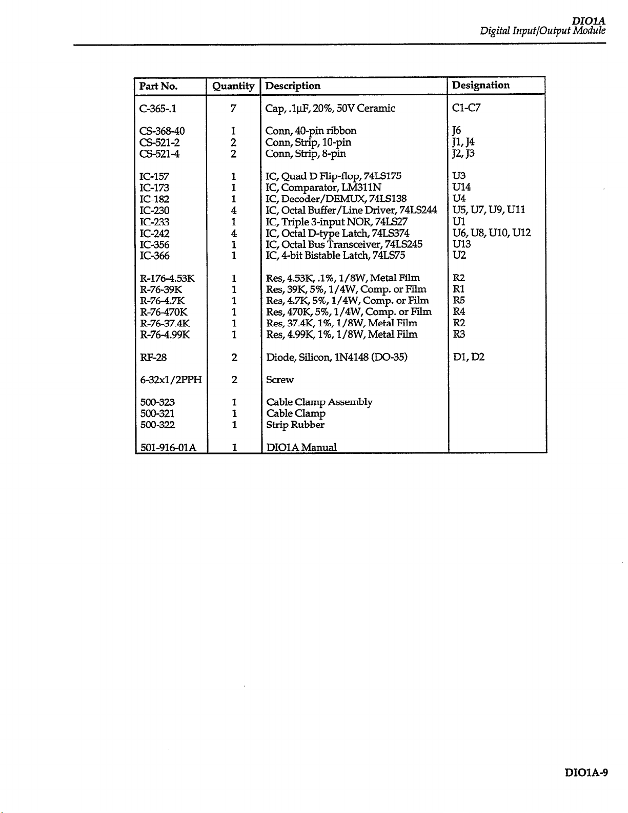
Part No.
C-365-.1
Cs-368-40
(X-521-2
(X-521-4
IC-157
IC-173 1
IC-182 1
IC-230
IC-233
IC-242
IC-356
IC-366 1
R-176-4.53K
R-76-39K
R-76-4.7K :
R-76-47OK
R-76-37.4K
R-76-4.99K
W-28 2
6-32xl/2PPH 2
Quantity Description
7 Cap, .l@?, 20%, 50V Ceramic
1
2 corm, strip, IO-pin
2 Conn, Strip, 8-pin
1
4
1
4
1
1
1
1
1
Designation
Cl-C7
Corm, 40-pin ribbon
IC, Quad D Flip-flop, 74LS175 u3
IC, Comparator, LM311N
IC, Decoder/DEMUX, 74LS138
IC, Octal Buffer/Line Driver, 74LS244 us, u7, u9, Ull
IC, Triple 3-input NOR, 74LS27
IC, Octal D-type Latch, 74LS374
IC, Octal Bus Transceiver, 74LS245 u13
IC, 4-bit B&able Latch, 74LS75 u2
Res, 4.53K, .I%, 1/8W, Metal Film R2
Res, 39K, 5%, 1/4W, Comp. or Film
Res, 4.7K, 5%, 1/4W, Comp. or Film E
Res, 47OK, 5%, 1/4W, Comp. or Film
Res, 37.4K, I%, 1/8W, Metal Film R2
Res, 4.99K, I%, 1 /SW, Metal Film R3
Diode, Silicon, lN4148 0X-35)
Screw
J6
JL J4
JZ
J3
u14
u4
Ul
US, U8, UlO, U12
R4
Dl, D2
500-323
500-321
500-322
501-916-OlA
1
1
1
1
Cable Clamp Assembly
Cable Clamp
Strip Rubber
DIOlA Manual
DIOlA-9
Page 10

I-
Page 11

-
Page 12
Using the DIOlA
and
KDAC500 Software
The DIOlA digital I/O module
can be used in a variety of control
and monitoring applications to
source and sense digital logic levels.
The module’s 32 channels can be
configured for input or output in
groups of 8 channels. Each group of
8 channels is a called a “port”. Port
A consists of channels O-7, port B
consists of channels 8-15, and so on.
The DIOlA channels can be read or
written individually, or as ports.
The DIOlA channels are nonisolated, meaning that DIOlA digital
ground is connected to earth
ground. Therefore, the low side of
any circuitry connected to the
DIOlA must also be at ground potential or the circuitry, DIOlA, or
data acquisition system may be
damaged.
DIOlA inputs and outputs are
compatible with low-power
Schottky transistor-transistor logic
(IS-‘ITLJ. This defines the voltage
and current levels associated with
logical high and low. When configured for input, each DIOlA channel presents one IS-TTL load to an
external circuit. The external circuit
must be able to absorb (sink) at least
0.4mA at O-O.5 volts for the DIOlA
to recognize an input signal as a
logic low. The same input must be
capable of sourcing at least 20@ at
2-5 volts to drive a DIOlA input
high.
A DIOlA output can drive up to
60 IS-TTL inputs, or 15 standard
TTL inputs. This corresponds to a
current sink capability of 24mA at O-
0.5 volts. Drive current available
from a high output is approximately
1mA at 2-5 volts.
Do not connect signals of less than
OV or greater than 5V to the DIOlA
or you may damage the module.
Connection to Digital
Logic
The DIOlA can interface many
types of digital circuitry and logic
families. However, it is important
that any external voltages applied to
the DIOlA inputs or outputs be
within the range of 0-5V. Any input
signal connected to the DIOlA must
have sufficient sink and source capability to drive at least one IS-ITL
load. Any load connected to a
DIOlA output must not cause the
DIOlA output to sink more than
24mA. Review the input and output
specifications for the type of logic
connected to the DIOlA to determine what conditioning, if any, may
be required. This information is
readily available in IC
manufacturers’ data books.
Page 13
Using the DIOIA and
KDAC500
The DIOlA can usually be
connected to standard T-l-L logic
without concern for voltage levels.
However, the total current loading is
important where one lTL output is
connected to several DIOlA inputs,
or where several external loads are
connected to one DIOlA output. A
variety of TTL sub-families exist,
including low- medium- and high-
power types. Each sub-family has
different current sink and source
specifications associated with input
and output. Make sure that a DIOlA
channel and the external logic can
each sink and source sufficient
current to control each other.
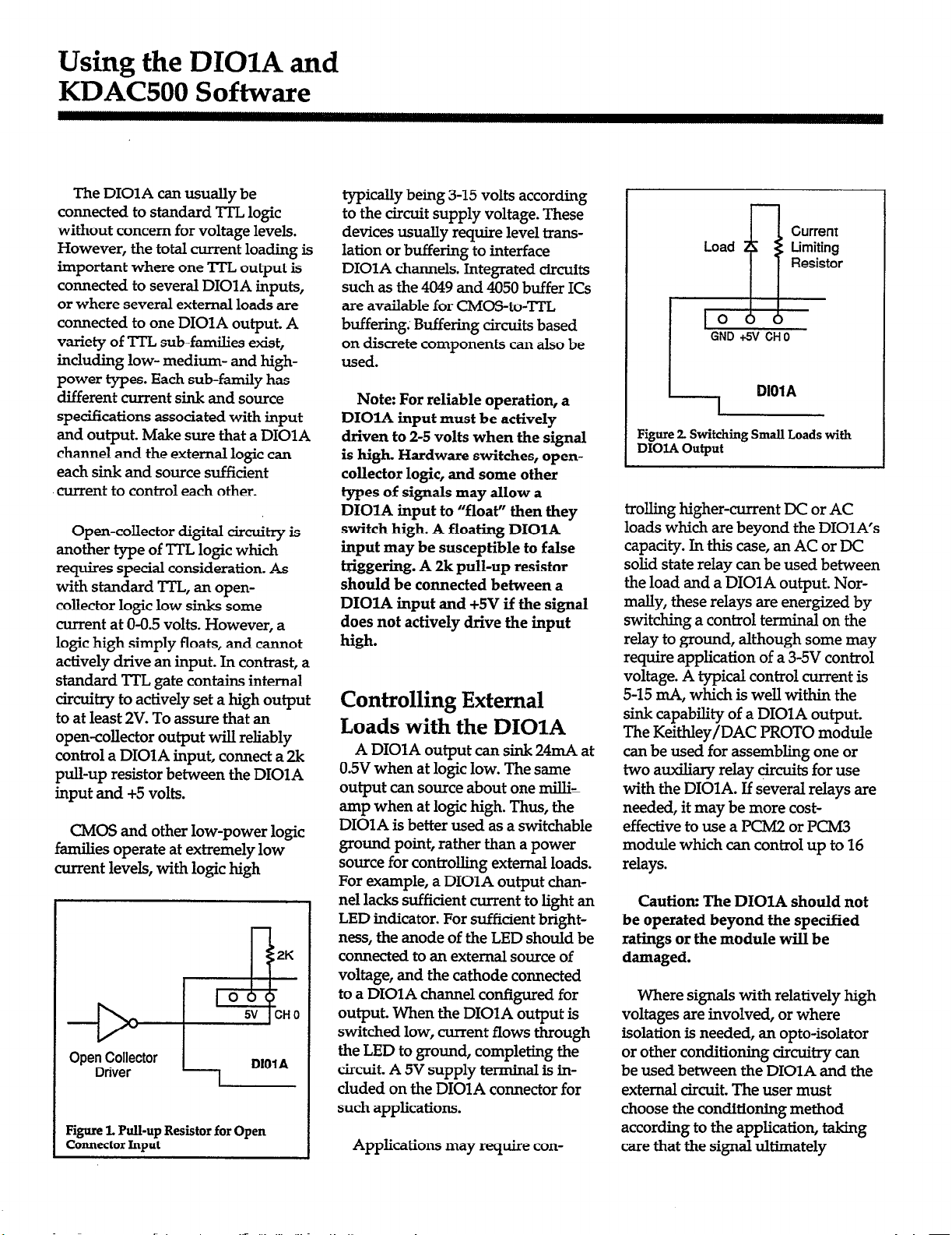
Open-collector digital circuitry is
another type of TTL logic which
requires special consideration. As
with standard TI’L, an opencollector logic low sinks some
current at O-O.5 volts. However, a
logic high simply floats, and cannot
actively drive an input. In contrast, a
standard TTL gate contains internal
circuitry to actively set a high output
to at least 2V. To assure that an
open-collector output will reliably
control a DIOlA input, connect a 2k
pull-up resistor between the DIOlA
input and +5 volts.
CMOS and other low-power logic
families operate at extremely low
current levels, with logic high
Open Collector
Driver
Figure 1. Pull-up Resistor for Open
Connector Input
Software
2K
I
06c$
5V ]CHO
DlOlA
typically being 3-15 volts according
to the circuit supply voltage. These
devices usually require level translation or buffering to interface
DIOlA channels. Integrated circuits
such as the 4049 and 4050 buffer ICs
are available for CMOS-to-TTL
buffering; Buffering circuits based
on discrete components can also be
used.
Note: For reliable operation, a
DIOlA input must be actively
driven to 2-5 volts when the signal
is high. Hardware switches, opencollector logic, and
types of signals may allow a
DIOlA input to “float” then they
switch high. A floating DIOlA
input may be susceptible to false
triggering. A 2k pull-up resistor
should be connected between a
DIOlA input and +5V if the signal
does not actively drive the input
high.
some
other
Controlling External
Loads with the DIOlA
A DIOlA output can sink 24mA at
05V when at logic low. The same
output can source about one mill&
amp when at logic high. Thus, the
DIOlA is better used as a switchable
ground point, rather than a power
source for controlling external loads.
For example, a DIOlA output channel lacks sufficient current to light an
LED indicator. For sufficient brightness, the anode of the LED should be
connected to an external source of
voltage, and the cathode connected
to a DIOlA channel configured for
output. When the DIOlA output is
switched low, current flows through
the LED to ground, completing the
circuit. A 5V supply terminal is included on the DIOlA connector for
such applications.
Applications may require con-
Load 2S :; Limiting
lo 0 b
GND +!3V CH 0
I L1
I
Figure 2. Switching Small Loads with
DIOlA Output
I
trolling higher-current DC or AC
loads which are beyond the DIOlA’s
capacity. In this case, an AC or DC
solid state relay can be used between
the load and a DIOlA output. Normally, these relays are energized by
switching a control terminal on the
relay to ground, although some may
require application of a 3-5V control
voltage. A typical control current is
5-15 mA, which is well within the
sink capability of a DIOlA output.
The Keithley/DAC PROTO module
can be used for assembling one or
two auxiliary relay circuits for use
with the DIOIA. If several relays are
needed, it may be more costeffective to use a PCM2 or PCM3
module which can control up to 16
relays.
Caution: The DIOlA should not
be operated beyond the specified
ratings or the module will be
damaged.
Where signals with relatively high
voltages are involved, or where
isolation is needed, an opto-isolator
or other conditioning circuitry can
be used between the DIOlA and the
external circuit. The user must
choose the conditioning method
according to the application, taking
care that the signal ultimately
I
, Current
Resistor
DIOlA
Page 14

Current Limiting
~~$g-~Lk+v
Figure 3. Opto-Isolator for Controlling Loads
applied to the DIOlA is within
acceptable limits. Where many
channels are involved, Keithley’s
DIM1 and DOMl digital I/O
modules offer 16 channels each, with
optical isolation and the ability to
interface voltages
up
to 2SV and
loads up to 50&L Both modules
maintain isolation of up to 500V
between channels, or from channel
to ground.
Monitoring the status of .
mechanical
switches presents two
problems. Where an application
must detect a contact closure, it is a
simple matter to connect the switch
+5v
1
^.,
Using the DIOlA and
KDAC500 Software
from
a DIOlA input to ground.
However, this method will allow the
DIOlA input to float when the
switch is opened. The channel may
be susceptible to noise or activity on
other channels. The solution is to
also connect a 2% pull-up resistor
between the DIOlA input channel
and +5V (Figure 4). When the switch
opens, the channel will be pulled to
+5V through the resistor, and be
immune to noise and false
triggering.
Second, mechanical switch
contacts usually exhibit ‘bounce”, in
which electrical continuity rapidly
makes and breaks several times at
the instant the contacts close. In
some digital applications, this
bounce may be unacceptable. The
solution is to use a “debouncing”
circuit between the switch and
DIOlA input. A flip-flop circuit
suitable for debouncing SPDT limit
switches is shown below. A second
Switoh at
position 2
Connection to
Mechanical Switches
2K
I
lo 6 0
GND +5V CHO
Figure 4. Mechanical SPST Switch with
Pull-up Resistor
Release
Figure 5. Debouncing Circuits
Page 15

Using the DIOAI and
KDAC500
remedy, ideal for debouncing
momentary push-button switches,
uses a circuit which generates a
single pulse when triggered by the
switch. The pulse must be longer
than the time it takes the contacts to
settle (typically a matter of milliseconds). A 555 timer integrated circuit or various types of one-shot ICs
can be used for this application. See
IC manufacturers’ data books for
more information.
Software
Reading BCD Outputs
Before IEEE488 and RS232-C
serial interfaces became the preferred method, binary-coded
decimal (BCD) outputs were included on some instruments to make
digitized data available to computers, calculators, or other digital
equipment. In principle, BCD uses
four lines to represent the numerals
O-9, but the actual encoding method
and number of digits varied among
manufacturers and instruments. A
multi-digit BCD readout might use
four separate lines for each digit,
resulting in many lines but relatively
simple decoding. Alternately, an
instrument might multiplex several
digits onto four lines plus a few
additional digit select lines, resulting
in fewer lines but more complicated
decoding.
With attention to signal levels and
the BCD encoding method, a DIOlA
can be used to read BCD lines. The
easiest method is to read the DIOlA
inputs as ports. This will return
eight data bits at one time. The
.
DIOlA’s 32 inputs can thus deal
with 6-8 BCD digits. If the digits are
multiplexed, the DIOlA can read an
unlimited number of digits, but the
requisite program will be more com-
plex. The decoding of the signals
must be done in software, and may
be based upon a look-up table or
some
calculation method.
Software Considerations
The DIOlA powers up with all
ports configured for input. Any
software used with the DIOlA must
be able to configure the module’s
ports for output if the application
requires digital output.
Keithley’s KDAC5OO software
provides complete control of all
DIOlA functions. The following
suggestions cover programming in a
BASIC or QuickBASIC environment,
but are equally useful in all
KDAC500 versions. Most applications of KDAC500 and the DIOlA
are simple in concept, and can be
summarized as follows:
1. Where one digital input reading
is required, a foreground read
(FGREAD) command can be used.
FGREAD will return the bit value
representing a single input channel,
or the byte value representing an
input port (8 channels).
Where a port is read, the values of
an individual bit within the byte can
be extracted by “ANDing” the byte
value with the weight of the bit’s
position. For example, the weight of
the most significant bit (MSB) in a
byte is 128. To test the value of the
MSB in the byte value “BV”, one
would execute the BASIC statement:
BT=BVAND128
If BT equals 0, the MSB value is 0,
otherwise the MSB value is 1.
Channel and bit values are covered
in more detail in the DIOlA manual.
2. Where values must be read
from a digital input channel at
regular intervals, a background read
(BGREAD) command should be
used. BGREAD will automatically
allocate and store the data in a
KDAC5OO memory array. If single
channels are being read, a KDAC500
bit array should be specified in the
BGREAD command. If ports are
being read, a KDACSOO byte array
should be specified in BGREAD.
The BGREAD command will
begin taking data when the
KDAC5OO INTON command is
executed. One data value will be
read when each interrupt fires. A
BGSTATUS command should be
used after the lNTON to determine
when all the data points have been
collected. Afterward, the individual
data values can be read from the
array by using an ARGET command
nested in a FOR-NEXT loop. If the
array is a byte array, the values of
individual bits in each byte can be
extracted by ANDing the byte
values with bit weights as described
above.
3. Where one digital value must be
programmed to a DIOlA output
channel or port, a foreground write
(FGWRITE) command is most convenient. FGWRITE can write a 0 or 1
to a single channel, or a byte value O255 to a port. The value of the byte
can be calculated by adding up the
weights of all the high bits in the
byte. For example, a port is to be
programmed with the bit values
11010011:
BYTE
WEIGHT
MSB
1:s d4 2 1’6 : 4 2 1
128+64+0+16+0+0 +2+ 1
TOTAL
LSB
0 1 1
-211
Page 16

Using the DIOAl and
KDAC500Software
The byte value 211 should be
written to the port.
4. Where several values must be
written to a digital output channel or
port, a background write
(BGWRITE) command should be
used.
Before BGWRlTE, a KDACSOO
array must be allocated with
ARMAKE to hold the output data. If
the data values are intended for a
single channel, the array must be a
bit array, and the data will consist ot
l’s and 0’s. If the data values are
intended for a port, the array should
be a byte array, and the data will
consist of values O-255. The array
must be long enough to hold the
desired number of data points.
The data values should be written
to the array using an AR??UT command. A FOR-NEXT loop around
ARPTJT may be helpful in reducing
the number of program lines need to
fill the array.
If the desired output is a simple
digital square wave, a single 1 and 0
can be written with ARPUT to a
two-deep, KDAC500 bit array.
If the output involves a more complex pattern of pulses, ARRJT can
be used to fill a longer KDAC500 bit
array with the necessary order of l’s
and 0’s.
If the output involves a digital
port, a KDAC500 byte array must be
used. The values of individual bytes
should be calculated as shown in the
weighting example above, and then
written to the array with ARMJT.
In all cases for BGWRlTE, output
will commence when interrupts are
turned on with INTON. One data
value will be written from the array
each time an interrupt fires. Note
that one complete cycle through an
array may require many interrupts,
so the period of square waves and
other pulses will probably not equal
the interrupt rate. BGWRITE’s
cycling parameter can be set for a
specific number of repeats, or for
continuous output of the array. If
cycling is not continuous, a
BGSTATUS command should be
used after INTON to determine
when all the data points have been
written.
Page 17

Data Acquisition and Control Division
Keithley Instrumegs, Inc. l 28775 Aurora Road l Cleveland, Ohio 44139 l (216) 2484400 l Fax: 349-4569
WEST GERMANY:
GREAT BRITAIN:
FRAXE Keithley Instruments SARL 03 All&z des Garays*B.P. 60 091124 Palaiseau/ZL l l-6-0115 155 l Telexz 600 933.F~ 1-6-0117726
NETHERLANDS:
SWITZERLAND:
AUSTRIA;
ITALYz Keithley Instruments SRL l Viale S. Giignano 4/A l 20146
Keithley Instruments GmbH l Heiglhofstr. 5 l Miinchen 70 l 089-71002-0 l Telex: 52-12160 l Fax: 089~7lOO25Q
Keithley Instruments, Ltd. l 1 Boulton Road l Reading, E&shire RG 2 ONL l 0734-861287 l Telex: 847 047 l Fax: 0734-863665
Keithley Instruments BV* Avelingen West 49 04202 MS GorincherwP.0. Box 559*42&l AN Gorinchan*OlS30-m*T& 24 684*Fax: 01830-30821
Keithley Instruments SA l Kriesbachstr. 4 l 86CO Diibendorf l 01-8219444 l Telex: 828 472 l Faxz 0222-315366
Keithley
Instruments
GesmbH l Rosenhiigelstrasse 12 0 A-1120 Vienna l (0222) 84 65 48 l Telex: 131677 l Fax: (0222) 84 35 97
Milan0 l
024120360 or 02-4156540 l Fax: 024121249
 Loading...