

Page 1
Technical Note
Differential Oscilloscope
Measurements
A Primer on Differential Measurements,
Types of Amplifiers, Applications, and
Avoiding Common Errors
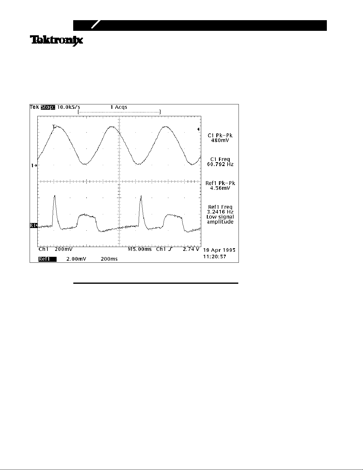
Simulated 4 mV
noise, using a conventional oscilloscope probe (upper). A differential amplifier extracts the signal from the noise
heartbeat waveform can not be measured in the presence of 500 mV
p-p
Introduction
All Measurements Are Two-Point
Voltage is always measured
between two points in a circuit. This is true whether
using a voltmeter or an oscilloscope. When an oscilloscope probe touches a point
in a circuit, a waveform usually appears on the display,
even if the ground lead is not
connected. In this situation,
the reference for the measurement is conducted
through the safety ground of
the scope chassis to the electrical ground in the circuit.
By virtue of their two probes,
digital voltmeters measure
potential between two
points. Because they are iso-
lated, these two points can
be anywhere in the circuit.
This has not always been the
case. Before the advent of the
digital voltmeter, hand-held
meters known as VOMs
(Volt-Ohm-Meters) were
used to measure “floating”
circuits. Because they were
passive, they tended to load
the circuit-under-test. Less
invasive measurements were
made with the highimpedance VTVM (Vacuum
Tube Volt Meter). The VTVM
had one major limitation –
the measurement was always
referenced to ground. The
VTVM housing was
grounded and connected to
the reference lead. With the
, 60 Hz common-mode
p-p
introduction of solid-state
gain circuits, high performance voltmeters could be
isolated from ground, allowing floating measurements to
be made.
Most oscilloscopes today,
like the venerable VTVM,
can only measure voltages
that are referenced to earth
ground, which is connected
to the scope chassis. These
are referred to as “singleended” measurements – the
probe ground provides the
reference path. Unfortunately, there are times when
this limitation lowers the
integrity of the measurement,
or makes measurement
impossible.
If the voltage to be measured
is between two circuit nodes,
neither of which is
grounded, conventional
oscilloscope probing cannot
be used. A common example
is measuring the gate drive in
a switching power supply
(see Figure 1).
Signals which are balanced
(between two leads without a
ground return) such as a
common telephone line cannot be measured directly. As
we shall see, even some
“ground referenced” signals
cannot be faithfully measured using single-ended
techniques.
When Ground Is Not Ground
We’ve all heard of “ground
loops” and been taught to
avoid them. But how do they
corrupt a scope measurement? A ground loop results
when two or more separate
ground paths are tied
Copyright © 1996 Tektronix, Inc. All rights reserved.
Page 2

Contents
Introduction · · · · · · · · · · · · · · · · · · · · · · · · · · · · · · 1
Differential Measurement Fundamentals · · · 4
Overview of Differential Measurements · · · · · · · 4
Common-Mode Rejection Ratio (CMRR) · · · · · · · 4
Other Specification Parameters · · · · · · · · · · · · · · 6
Differential-mode range · · · · · · · · · · · · · · · · · · · 6
Common-mode range · · · · · · · · · · · · · · · · · · · 6
Maximum common-mode slew rate · · · · · · · · · 6
Types of Differential Amplifiers and Probes · · · · 7
Built-in differential amplifiers · · · · · · · · · · · · · · 7
High-voltage differential probes. · · · · · · · · · · · 7
High-gain differential amplifiers · · · · · · · · · · · · 8
High-performance differential amplifiers · · · · · 8
Differential passive probes · · · · · · · · · · · · · · · · 8
High-bandwidth active differential probes · · · · 8
Voltage Isolators · · · · · · · · · · · · · · · · · · · · · · · 8
Figure 1. Gate drive signal in a switching power supply is measured between TP1 and
TP2. Neither point is grounded.
Differential Measurement Applications · · · · · 9
Power Electronics · · · · · · · · · · · · · · · · · · · · · · · · · 9
System Power Distribution · · · · · · · · · · · · · · · · · · 9
Balanced Signals · · · · · · · · · · · · · · · · · · · · · · · · 10
Transducers · · · · · · · · · · · · · · · · · · · · · · · · · · · · 10
Biophysical Measurements · · · · · · · · · · · · · · · · 11
Maintaining Measurement Integrity · · · · · · · 11
Sources of Measurement Error · · · · · · · · · · · · · 11
Input Connections · · · · · · · · · · · · · · · · · · · · · · · · 11
Grounding · · · · · · · · · · · · · · · · · · · · · · · · · · · · · · 11
Input Impedance effects on CMRR · · · · · · · · · · · 13
Common-Mode Range · · · · · · · · · · · · · · · · · · · · 13
Measuring Totally Floating Signals · · · · · · · · · · 14
Bandwidth · · · · · · · · · · · · · · · · · · · · · · · · · · · · · · 14
Glossary · · · · · · · · · · · · · · · · · · · · · · · · · · · · · · · · 15
Related Publications from Tektronix · · · · · · · 16
Figure 2. Ground loop formed by a scope probe. Metal chassis of both scope and device
under test are connected to safety ground and internal power supply common. Scope
probe ground connects to scope chassis at the input BNC connector.
together at two or more
points. The result is a loop of
conductor. In the presence of
a varying magnetic field, this
loop becomes the secondary
of a transformer which is
essentially a shorted turn.
The magnetic field which
excites the transformer can
be created by any conductor
in the vicinity which is carrying a non-DC current. AC
line voltage in primary
wiring or even the output
lead of a digital IC can produce this excitation. The current circulating in the loop
impedance within the loop.
Thus, at any given instant in
time, various points within a
ground loop will not be at
the same potential.
Connecting the ground lead
of an oscilloscope probe to
the ground in the circuitunder-test results in a ground
loop if the circuit is
“grounded” to earth ground
(see Figure 2). A voltage
potential is developed in the
probe ground path resulting
from the circulating current
acting on the impedance
within the path.
develops a voltage across any
page 2
Page 3
Thus, the “ground” potential
at the oscilloscope’s input
BNC connector is not the
same as the ground in the
circuit being measured (i.e.,
“ground is not ground”).
This potential difference can
range from microvolts to as
high as hundreds of millivolts. Because the oscilloscope references the measurement from the shell of
the input BNC connector, the
displayed waveform may not
represent the real signal at
the probe input. The error
becomes more pronounced
being measured decreases, as
is common in transducer and
biomedical measurements.
In these situations, it’s often
tempting to remove the probe
ground lead. This technique
is only effective when measuring very low-frequency
signals. At higher frequencies, the probe begins to add
“ring” to the signal caused by
the resonant circuit from the
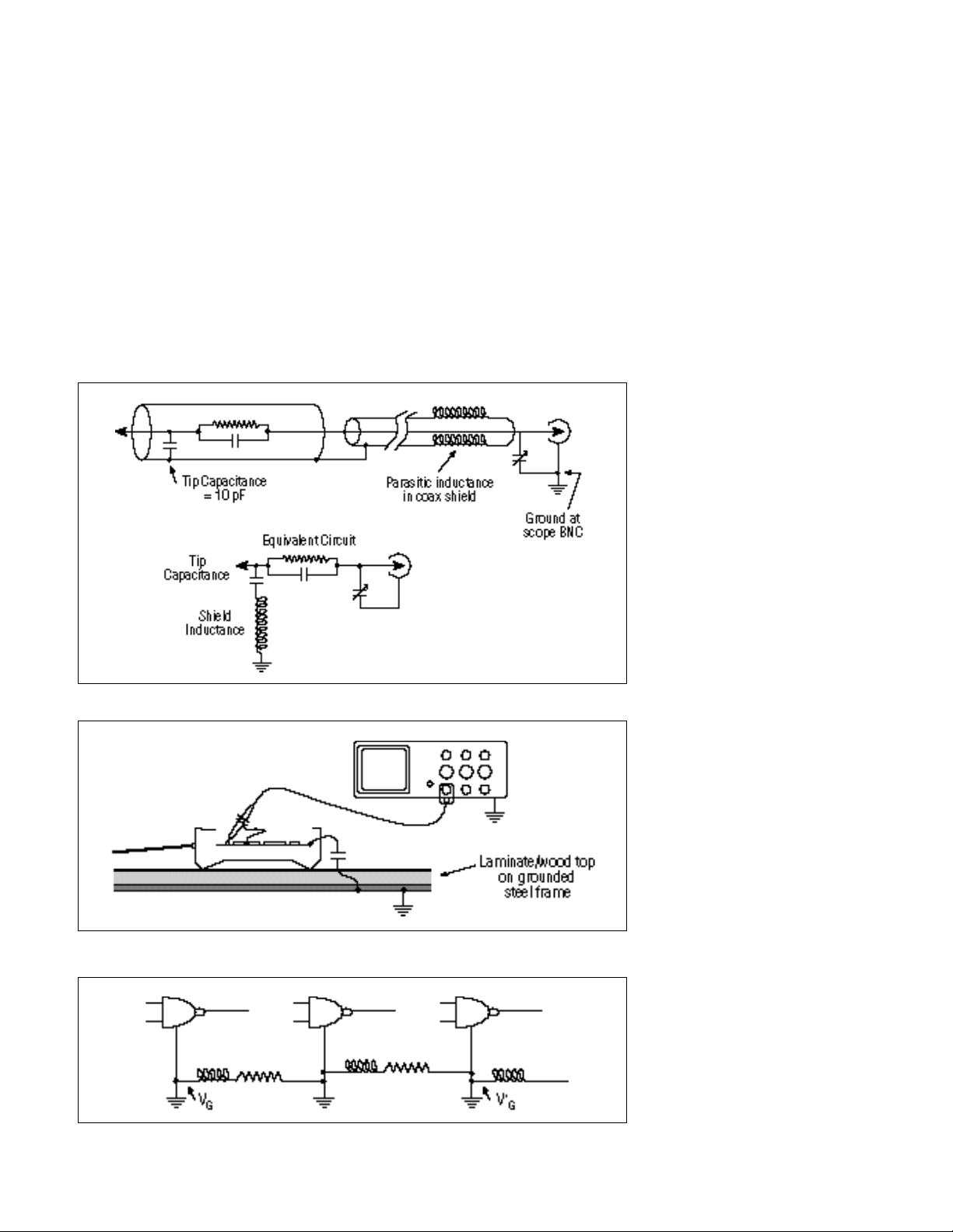
tip capacitance and shield
inductance (see Figure 3).
(This is why you should
always use the shortest
ground lead possible.)
as the amplitude of the signal
Figure 3. Series resonant tank circuit formed by probe-tip capacitance and ground inductance.
Figure 4. “Floating” battery-powered cellular telephone probed with a grounded oscilloscope. Capacitance
between the phone circuitry and steel bench frame forms a virtual ground loop at high frequencies.
Figure 5. Minute parasitic inductance and resistance in ground distribution system result in VG≠ V'G.
We now have a dilemma:
create a ground loop and add
error to the measurement or
remove the probe ground
lead and add ring to the
waveform!
The next technique often
tried to break ground loops is
to “float” the scope or “float”
the circuit being measured.
“Floating” refers to breaking
the connection to earth
ground by opening the
safety-ground conductor –
either at the device-undertest or at the scope. Floating
either the scope or the
device-under-test (DUT)
allows the use of a short
ground lead to minimize ring
without creating a ground
loop.
This practice is inherently
dangerous, as it defeats the
protection from electrical
shock in the event of a short
in the primary wiring. (Some
special battery-operated
portable scopes incorporate
insulation which allows safe
floating operation.) Operator
safety can be restored by
placing a suitable groundfault circuit interrupter
(GFCI) in the power cord of
the oscilloscope (or deviceunder-test) with the severed
ground. However, be aware
that without a lowimpedance ground connection, radiated and conducted
emissions from the scope
may now exceed government
standards – as well as interfere with the measurement
itself. At higher frequencies,
severing the ground may not
break the ground loop as the
“floating” circuit is actually
coupled to earth ground
through stray capacitance
(see Figure 4).
Even when the measurement
system doesn’t introduce
ground loops, the “ground is
not ground” syndrome may
exist within the device being
measured (see Figure 5).
Large static currents and
high-frequency currents act
on the resistive and induc-
page 3
Page 4

tive components of the
device ground path to produce voltage gradients. In
this situation, the “ground”
potential referenced at one
point in the circuit will be
different than that referencing another point.
For example, ground at the
input of the high-gain amplifier in a system differs from
the “ground” potential at the
power supply by several
millivolts. To accurately
measure the input signal
seen by the amplifier, the
probe must reference the
ground at the amplifier input.
These effects have challenged designers of sensitive
analog systems for years. The
same effect is seen in fast
digital systems. The small
inductance within the
ground distribution system
can create a potential across
it, resulting in “ground
bounce”. Troubleshooting
systems affected by groundvoltage gradients is difficult
because of the inability to
really look at the signal
“seen” at the individual component. Connecting the oscilloscope probe ground lead to
the “ground” point of the
device results in the uncertainty of what effects the new
path adds to the ground gradient. A sure clue that a
change is occurring is seen
when the problem in the circuit either gets better (or
worse) when the probe
ground is connected. What
we really need is a method to
make a scope measurement
of the actual signal at the
input of the suspect device.
By using an appropriate differential amplifier, probe, or
isolator, accurate two-point
oscilloscope measurements
can be made without introducing ground loops or otherwise corrupting the measurement, upsetting the
device-under-test, or exposing the user to shock hazard.
There are several types of
differential amplifiers and
isolation systems available
for oscilloscopes, each optimized for a particular class
of measurements. In order to
choose the proper solution,
an understanding of terminology is necessary.
Overview of Differential
Measurements
An ideal differential amplifier amplifies the “difference”
signal between its two inputs
and totally rejects any voltage
which is common to both
inputs (see Figure 6). The
transfer equation is:
VO= AV( V
where VOis referenced to
earth ground.
The voltage of interest, or
difference signal, is referred
to as the differential voltage
or differential mode signal
and is expressed as V
is the V
transfer equation above).
Figure 6. Differential amplifier.
page 4
+in
Differential Measurement Fundamentals
The voltage which is common to both inputs is
referred to as the CommonMode Voltage expressed as
. The characteristic of a
V
CM
differential amplifier to
is referred to
CM
+ i n
– V
– V
)
– i n
term in the
–in
DM(VDM
ignore the V
as Common-Mode Rejection
or CMR. The ideal differential amplifier rejects all of the
common-mode component,
regardless of its amplitude
and frequency.
In Figure 7, a differential
amplifier is used to measure
the gate drive of the upper
MOSFET in an inverter circuit. As the MOSFET switches
on and off, the source voltage
swings from the positive sup-
ply rail to the negative rail. A
transformer allows the gate
signal to be referenced to the
source. The differential amplifier allows the scope to measure the true V
signal (a few
G S
volt swing) at sufficient resolution such as 2 V / d i v i s i o n
while rejecting the several
hundred volt transition of the
source to ground.
Common-Mode Rejection Ratio
( C M R R )
Real implementations of differential amplifiers cannot
reject all of the common
mode signal. A small amount
of common mode appears as
an error signal in the output,
making it indistinguishable
from the desired differential
signal. The measure of a differential amplifier’s ability to
eliminate the undesirable
common-mode signal is
referred to as Common-Mode
Rejection Ratio or CMRR for
short. The true definition of
CMRR is “differential-mode
gain divided by commonmode gain referred to the
input”:
A
CMRR =
D M
A
C M
Page 5

Figure 7. Differential amplifier used to measure gate to source voltage of upper transistor in an inverter bridge.
Note that the source potential changes 350 volts during the measurement.
Figure 8. Common-mode error from a differential amplifier with 10,000:1 CMRR.
For evaluation purposes, we
can assess CMRR performance with no input signal.
The CMRR then becomes the
apparent V
put resulting from common
mode input. It’s expressed
either as a ratio – 10,000:1 –
or in dB:
dB = 20log
A CMRR of 10,000:1 would
be equivalent to 80 dB.
seen at the out-
DM
V
D M
(
)
V
C M
For example, suppose we
need to measure the voltage
in the output damping resistor of an audio power amplifier as shown in Figure 8. At
full load, the voltage across
the damper (V
reach 35 mV, with an output
swing (VCM) of 80 V p-p. The
differential amplifier we use
has a CMRR specification of
10,000:1 at 1 kHz. With the
amplifier driven to full
power with a 1 kHz sine
) should
DM
wave, one ten thousandth of
the common-mode signal
will erroneously appear as
at the output of the dif-
V
DM
ferential amplifier, which
would be 80 V/10,000 or
8 mV. The 8 mV represents
up to a 22% error in the true
35 mV signal!
The CMRR specification is
an absolute value, and does
not specify polarity (or
degrees of phase shift) of the
error. Therefore, the user can
not simply subtract the error
from the displayed waveform. CMRR generally is
highest (best) at DC and
degrades with increasing frequency of V
ential amplifiers plot the
CMRR specification as a
function of frequency.
Let’s look at the inverter circuit again. The transistors
switch 350 V and we expect
about a 14 V swing on the
gate. The inverter operates at
30 kHz. In trying to assess
the CMRR error, we quickly
run into a problem. The common-mode signal in the
inverter is a square wave,
and the CMRR specification
assumes a sinusoidal common-mode component.
Because the square wave
contains energy at frequencies considerably higher than
30 kHz, the CMRR will probably be worse than specified
at the 30 kHz point.
Whenever the common-mode
component is not sinusoidal,
an empirical test is the
quickest way to determine
the extent of the CMRR error
(see Figure 9). Temporarily
connect both input leads to
the MOSFET source. The
scope is now displaying only
the common-mode error. You
can now determine if the
magnitude of the error signal
is significant. Remember, the
phase difference between
and VDMis not specified.
V
CM
Therefore subtracting the displayed common-mode error
from the differential mea-
. Some differ-
CM
page 5
Page 6

Figure 9. Empirical test for adequate common-mode rejection. Both inputs are driven from the same point. Residual common mode appears at the output. This test will not catch the effect of different source impedances.
surement will not accurately
cancel the error term.
This is a handy test for determining the extent of common-mode rejection error in
the actual measurement environment. However there’s
one effect this test will not
catch. With both inputs connected to the same point,
there’s no difference in driving impedance as seen by the
amplifier. This situation produces the best CMRR performance. When the two inputs
of a differential amplifier are
driven from significantly different source impedances,
the CMRR will be degraded.
The specifics of the effect are
discussed later – see Input
Impedance Effects on
CMRR, page 13.
Other Specification Parameters
Differential-mode range is
equivalent to the input range
specification of an amplifier
or single-ended oscilloscope
input. Input voltages which
exceed this range will overdrive the amplifier, resulting
in output clipping or nonlinearity.
Common-mode range refers
to the voltage window over
which the amplifier can
reject the common-mode signal. The common-mode
range is usually larger than
or equal to the differential
range. Depending on the
amplifier topology, the common-mode range may or may
not change with different
amplifier gain settings.
Exceeding an amplifier’s
common-mode range may
have various results in the
output. In some situations,
the output will not clip and
may produce a close approximation of the true input,
with some additional offset.
In this situation, the display
may be close enough to what
is expected that it’s not questioned by the user. It’s
always a good practice to
verify that the commonmode signal is within the
acceptable common-mode
range before making any differential measurements.
Maximum common-mode
slew rate is specified for
some differential amplifiers
and most isolators. This
specification is often confusing but very important. Part
of the confusion results from
a lack of standard definition
between instrument manufacturers. Also, differential
amplifiers and isolators
behave differently when
their maximum commonmode slew rate is exceeded.
Essentially, maximum CM
slew rate is a supplemental
specification to CMRR. The
specification is usually given
in units of kV/µs.
Some types of differential
amplifiers, like other amplifiers, reach a large-signal
slew rate limitation before
the small-signal bandwidth
specification is exceeded.
When one or both sides of a
differential amplifier are
driven to slew-rate limiting,
the common-mode rejection
is degraded very rapidly.
Unlike CMRR, maximum
slew rate does not imply an
increasing amount of common-mode feed-through in
the output. Once the maximum common-mode slew
rate is exceeded, all bets are
off – the output is likely to
clamp at one of the power
supply rails.
In isolators, however, the
effect is more gradual – like
CMR in a differential amplifier. As the common-mode
slew rate increases (as
opposed to the frequency),
more of the common-mode
component “feeds through”
to the output. Intuitively, the
specification would imply a
maximum slew rate at which
a known amount of feedthrough appears in the output. It’s important to note
that with some isolators, the
CM slew rate specification is
actually a maximum nondestructive limit. The ability
to make meaningful measurements is lost at slew rates
much lower than the maximum specification. When
using an isolator, it’s best to
test the common-mode feedthrough before making critical measurements. This is
easily done by driving both
the probe tip and the reference lead with the same
common-mode signal and
observing the output.
page 6
Page 7

Types of Differential Amplifiers
and Probes
Built-in differential amplifiers. Many scopes have the
ability to make the simplest
differential measurements
built right in to them. This
mode is referred to as “channel A – channel B” or “quasidifferential”. While limited
in performance, this technique may be adequate for
some measurements. To
make a differential measurement, two vertical channels
are used – one for the positive input and one for the
negative input. The channel
used for negative input is set
to invert mode and the display mode is set to “ADD
Channel A + Channel B”. For
proper operation, both inputs
must be set to the same scale
factor, and both input probes
must be identical models.
The display now shows the
difference voltage between
the two inputs.
To maximize CMRR, the gain
in both channels should be
matched. This can be easily
done by connecting both
probes to a square wave
source with an amplitude
within the dynamic range of
the volts/division setting
(about ±6 divisions). Set one
of the channels to “uncalibrated – variable” gain and
Figure 10. Even when the scope is “floating”, parasitic capacitance forms an AC voltage divider which adds error to
the measurement. Note that reversing the probe leads will load the gate with >100 pF, possibly destroying the circuit-
adjust the variable-gain control until the displayed waveform becomes a flat trace.
The primary limitation of
this technique is the rather
small common-mode range,
which results from the
scopes vertical channel
dynamic range. Generally,
this is less than ten times the
volts/division setting from
ground. Whenever
> VDM, this mode of
V
CM
obtaining a differential result
can be thought of as extracting the small difference from
two large voltages.
Most digital storage oscilloscopes perform waveform
math in the digital domain,
after the analog signal has
been digitized. The limited
resolution of the analog-todigital converter is often not
adequate to view the resulting differential signal after
the common-mode signal is
subtracted out. Because the
AC gain in the two channels
is not precisely matched,
CMRR at higher frequencies
is rather poor.
This technique is suitable for
applications where the common-mode signal is the same
or lower amplitude than the
differential signal, and the
common-mode component is
DC or low frequency, such as
50 or 60 Hz power line. It
effectively eliminates ground
loops when measuring signals of moderate amplitude.
High-voltage differential
probes. Recently, high-volt-
age active differential probes
have appeared on the market.
A new topology using fixed
attenuation with switchable
differential gain allows these
probes to keep their full common-mode range in all gain
settings. The single attenuator greatly reduces complexity resulting in lower cost to
the user.
These probes provide an
affordable, safe method of
measuring line-connected circuits commonly found in
switching power supplies,
power inverters, motor drives,
electronic-lamp ballasts, etc.
With common-mode ranges
up to 1,000 V, these probes
eliminate the need for the
extremely dangerous practice
of “floating the scope”.
Recently, workplace hazard
monitoring organizations
such as the U.S. OSHA (Occupational and Safety and
Health Act) have intensified
their verification of equipment grounding, issuing
costly fines to violators.
In addition to the safety benefits, the use of these probes
can improve measurement
quality. An obvious benefit is
the full use of the scopes multiple channels with the simultaneous viewing of multiple
signals referenced to different
voltages. Because the probes
are true differential, both of
the inputs are high
impedance – high resistance
and low capacitance. Floating
scopes and isolators do not
have balanced inputs. The
reference side (the “ground”
clip on the probe) has a significant capacitance to ground.
Any source impedance the
reference is connected to will
be loaded during fast common-mode transitions, attenuating the signal.
Worse yet, the high capacitance can damage some cir-
page 7
Page 8

cuits (see Figure 10). Connecting the scope common to
the upper gate in an inverter
may slow the gate-drive signal, preventing the device
from turning off and destroying the input bridge. This
failure is usually accompanied with a miniature fireworks display right on your
bench – something many
power electronics designers
can attest to.
With the balanced low input
capacitance of high-voltage
differential probes, any point
in the circuit can be safely
probed with either lead.
High-gain differential amplifiers. A high-gain differential
amplifier, often an external
accessory, allows scopes to
measure very small amplitude signals – down to a few
microvolts. To avoid corruption from ground-loop and
ground-gradient effects, these
signals are always measured
differentially – even when
they are ground referenced.
When the source is not
ground referenced, the common-mode can be several
orders of magnitude greater
than the differential mode
signal of interest. To cope
with this, these amplifiers
have extremely high CMRR,
often 1,000,000:1 or greater.
Some high-gain differential
amplifiers include additional
functionality to improve the
integrity of low-amplitude
measurements. Selectable
low-pass filtering allows the
user to remove out-of-band
noise from lower-frequency
signals. Differential offset can
be used to remove galvanic
potentials introduced in the
input wiring or transducerbridge bias voltage. To allow
use with signal sources which
have high driving impedance,
some models allow the user
to set the input to virtually
infinite impedance.
As with any differential
amplifier, the slightest mismatch in channel gain
greatly reduces the ampli-
fier’s high CMRR. When the
application requires use of a
scope probe, only identical
non-attenuating (1X) models
should be used, as attenuating probes can not be
matched well enough to preserve the CMRR.
High-performance differential amplifiers. With the
advent of oscilloscopes with
plug-in amplifiers, high-performance differential amplifiers became available. These
amplifiers combined many
features to allow their use in
diverse applications. Calibrated slideback allowed the
amplifiers to be used in single-ended mode, with the
trace referenced thousands of
divisions away from ground.
This makes it possible to precisely measure ripple valley
in power supplies and power
amplifier headroom. Sophisticated high-speed clamp circuits enable the amplifier to
quickly recover from input
overloads hundreds of times
over-range. This provides the
ability to directly measure
settling time of amplifiers
and DAC circuits.
These amplifiers feature
bandwidth specifications of
100 MHz or more, with good
CMRR as well. However,
the CMRR is specified with
both inputs tied directly
together and driven from a
low-impedance source. In
an actual application, the
CMRR at higher frequencies
will be considerably
degraded by differences in
source impedance and
channel gain.
Differential passive probes.
To minimize this degradation, only specially matched
differential passive probes
should be used with these
amplifiers. Be sure to calibrate the individual probe to
the amplifier using the procedure provided by the probe
manufacturer.
High-bandwidth active differential probes. These
probes maintain high-fre-
quency CMRR by buffering
the signal right at the probe
tip, thereby eliminating the
degradation caused by passive probe cables. These
probes have high bandwidth
(100 MHz or more), high-sensitivity, and excellent highfrequency CMRR performance. They are commonly
used to perform measurements in disk-drive read
electronics, where the signals
are inherently differential.
Their use is becoming more
common in probing highspeed digital circuits as they
do not alter the ground gradient when searching for
ground-bounce problems.
Voltage isolators. While voltage isolators are not really
differential amplifiers, they
provide a means of safely
measuring floating voltages.
Compared with differential
amplifiers, isolators have
advantages as well as tradeoffs, and the selection of one
over the other depends on
the application. As the name
implies, isolators have no
direct electrical connection
between the floating inputs
and their ground-referenced
output. The signal is coupled
via optical or split-path optical/transformer means. Two
physical configurations are
available: integrated onepiece systems and split transmitter/receiver systems.
The models with separate
transmitters and receivers are
interconnected with fiberoptic cable. The transmitter,
which is powered by
rechargeable batteries, can be
remotely located from the
receiver. This is useful in situations where the signal
originates in environments
not hospitable to humans or
oscilloscopes. They can also
be used with very high common-mode voltages. The
floating voltage specification
is usually limited by the
insulation voltage of the
hand-held probe. If the probe
connections can be made
with the DUT powered off,
page 8
Page 9

Figure 11. Unequal input capacitance caused by the isolated shield. This forms an AC voltage divider, resulting in the Vref’ ≠ Vref at the probe clip.
the floating voltage is limited
only by the physical separation between the transmitter
and ground.
Because isolators have no
resistive path to ground, they
are a good choice for applications which are extremely
sensitive to leakage currents.
Circuits equipped with sensitive GFCI (Ground Fault Circuit Interrupters), such as
medical electronics, may
experience GFCI tripping
when connected to a differential amplifier. The lack of
ground terminated attenuators also gives isolators infi-
nite CMRR with static (DC)
common-mode voltages.
The disadvantage of isolators
is the fact that they are not
true differential amplifiers,
meaning that the input is not
balanced (see Figure 11). The
capacitance to earth ground
is considerably different in
the measurement (+) input
and the reference (–) input.
This results in the same problems as already described
when floating scopes. Source
impedance in the reference
lead forms an attenuator at
high frequencies with the
ground capacitance.
These problems can be minimized by connecting the reference to the point in the circuit with the lowest driving
impedance (invert the scope
channel to regain correct
polarity if necessary). If the
isolator has separate transmitter and receiver units,
physically isolate the transmitter from grounded surfaces as much as possible to
minimize capacitive coupling to ground. Placing the
transmitter on a cardboard
box or wooden crate can
make a marked improvement
in performance!
Differential Measurement Applications
Power Electronics
High-voltage differential
amplifiers provide an ideal
means of measuring circuits
which are line connected,
such as switching power
supply primaries, motor
drives, electronic-lamp ballasts, and similar systems.
They eliminate the need for
the dangerous practice of
“floating the scope”. The low
input capacitance will not
affect operation of inverters
by loading down gate-drive
circuits.
The characterization of
power switching devices
such as MOSFETs and IGBTs
often includes measuring
dynamic saturation characteristics. High-performance
differential amplifiers with
high-speed input clamps
allow accurate measurement
of turn-on saturation,
nanoseconds after being
overdriven (hundreds of
times full scale) when the
device was off. This allows
the use of the high sensitivities necessary to accurately
measure the saturation characteristics.
These amplifiers are also useful when measuring sec-
ondary circuits. By activating
the calibrated slideback (also
known as comparison voltage), the amplifier can be used
in a single-ended mode to
monitor ripple valley and linear-regulator headroom (see
Figure 12). With the slideback
set to the output voltage, the
headroom can be directly
V
C E
measured, at high sensitivity,
under a variety of dynamic
load conditions.
System Power Distribution
Developing high-precision
analog, mixed signal, and
high-speed digital systems
often involves troubleshoot-
page 9
Page 10

Figure 12. Using calibrated slideback to accurately measure power-supply ripple valley on the collector of the output regulator. Note that the scope is set to 100 mV/division with ground being 61 divisions off screen.
Figure 13. A transducer in balanced bridge configuration. A differential measurement is made between the taps of
the two divider legs.
ing power-distribution problems. These can be a
designer’s worst nightmare.
CAD systems offer little help
as the minute parasitics
which create these problems
are difficult or impossible to
model. A scope equipped
with a differential amplifier
is the best tool to track down
and pin-point the trouble
spots in the system.
Single-ended measurements
often hide power-distribution problems as they provide an alternate ground path
from which the signal is
measured. Not only does this
change the measurement, it
often affects the circuit operation as well – either improving or degrading it.
Placing the inputs of a differ-
power supply lead gives a
true picture of the device’s
power condition. Lead
inductance in logic devices
often isolates the IC from
local bypassing capacitance.
Even if the power supply
looks clean, both the ground
and power pins may be moving with respect to other
grounds in the system. By
moving the probe, it’s possible to track down dynamic
ground gradients between an
individual device ground
and other grounds in the system. The effects of ground
bounce in digital systems can
be easily measured. Probing
between an IC’s input and its
ground pin gives a picture of
the actual signal as seen by
that device.
ential probe right on an IC’s
Balanced Signals
Some systems employ signals which are inherently
differential in nature. When
both sides of the signal share
the same driving impedance
they are said to be balanced.
Balanced systems are common in professional audio
equipment, telephony, and
magnetic recording systems
(analog and digital memory)
to name a few. Differential
signal distribution is becoming more common in highspeed digital systems as well.
Ineffective attempts to measure these signals one side at
a time and “adding” the
results are error prone at
best. Often, loading only one
side of the signal with the
probe diverts energy to the
side not being measured.
Measuring a balanced system
differentially provides a true
picture of the signal.
Transducers
Differential measurements
are used universally in transducer systems. The small signal amplitudes and necessity
to eliminate ground loops
preclude the use of singleended measurements. The
word “transducer” brings to
mind connotations of devices
used for measuring mechanical phenomena such as
acceleration, vibration, pressure, etc. The application of
differential measurement
techniques goes beyond
these to include visual and
medical imagers, microphones, chemical sensors…
the list is endless.
Transducers which produce
a change in resistance are
often operated in a configuration known as a balanced
bridge (see Figure 13). This
configuration uses three
known resistances and the
transducer to produce a pair
of voltage dividers. The pair
is biased with a bridge supply and the voltage is measured differentially between
the divider taps. The advantage of this configuration is
page 10
Page 11

the elimination of the effects
of power supply fluctuations.
Often, a transducer produces
a DC output voltage representing the steady state
before excitation is placed in
the system. To get high resolution, it’s desirable to
remove the DC component.
AC coupling the amplifier
input is not effective if very
low-frequency components
(<2 Hz) need to be measured.
To accommodate this need,
many high-gain differential
amplifiers incorporate a differential offset feature. This
effectively inserts a floating,
adjustable power supply in
series with one of the inputs,
allowing the amplifier to
remain DC coupled. The offset control has considerable
range – as much as ±1 million divisions at the higher
gain settings.
Biophysical Measurements
CAUTION: Do not connect
any electrical instrument,
including a differential
amplifier, to a human subject unless it is specifically
designed for use on
humans. Suitable equipment will be certified to a
specific regulatory standard
as mandated by the individual country where it is used.
Measuring the electrical signals resulting from neurological activity presents several
challenges. The signals have
minute amplitudes – often
below a millivolt. The common-mode component can
be hundreds or even thousands of times greater than
the signal of interest. The
source impedance is rather
high. Usually, the differential
signal is corrupted with
high-amplitude noise. Fortunately, high-gain differential
amplifiers are equipped to
measure these signals.
CMRR specifications of
1,000,000:1 or more can
effectively eliminate the
common-mode component.
To deal with the high input
impedance, the amplifier can
be configured to infinite
input resistance mode. (Note
that if the specimen is not
shunted to ground by other
equipment, a separate probe
tied through a 100 kohm
resistor to ground should be
used to reduce the chance of
common-mode range overload.) Skin contact is usually
made with silver/silver chloride electrodes. These provide an ionic connection to
the specimen. They also generate a galvanic cell (battery)
with a half-cell voltage of
400 mV which adds a bias
voltage to the measurement.
The amplifier’s differential
offset can be used to remove
the bias while preserving
low-frequency response.
Because most biophysical
activity occurs at frequencies
below 20 Hz, bandwidth-limiting filters can be used to
reduce higher-frequency differential noise without altering the signal of interest.
Maintaining Measurement Integrity
Sources of Measurement Errors
Just like other measurements,
differential measurements
are subject to conditions
which generate errors. These
errors may or may not be
obvious in the results, and
Figure 14. Simplified schematic of a differential amplifier with attenuator.
may be misread as the
desired measurement. Some
of the more common sources
of error are covered below.
To understand what causes
these errors and how to
avoid them, we first need a
basic understanding of
what’s inside a differential
oscilloscope or probe.
The heart of the system is the
differential amplifier stage
(see Figure 14). The
schematic symbol is the
same as an op amp. Like the
operational amplifier, a differential amplifier rejects the
input common-mode signal
and only amplifies the voltage difference between the
two inputs. Unlike the op
amp, the differential amplifier has a known, finite gain.
In some configurations, the
gain is user-selectable. The
output is singled-ended and
referenced to ground. The
inputs are often FETs to give
very high impedance. The
input signal may pass
through a high-impedance
attenuator to reduce larger
signals to a range the ampli-
page 11
Page 12

fier can handle. The
demands on the attenuator
are much greater than those
in a single-ended amplifier.
Both sides must have identical DC and AC attenuation.
The amount of mismatch has
a first-order effect on the
CMRR. For example, to
maintain a 100,000:1 CMRR
specification, the attenuators
must match to better than
one part in 100,000
(0.001%); this leaves no margin for error in the differential amplifier! Of course, this
match needs to be maintained all the way from the
signal source.
Input Connections
Interconnecting the differential amplifier or probe to the
signal source is generally the
greatest source of error. To
maintain the input match,
both paths should be as identical as possible. Any cabling
should be of the same length
for both inputs. If probes are
used, they should be the
Figure 15. Time varying magnetic fields passing through the open leads induce a voltage as in a transformer
winding. This voltage appears as a differential component to the amplifier and is summed into the true VDMsig-
Figure 16. With the input leads twisted together, the loop area is very small, hence less field passes through it.
Any induced voltage tends to be in the VCMpath which is rejected by the differential amplifier.
same model and length.
When measuring low-frequency signals with large
common-mode voltages,
avoid the use of attenuating
probes. At high gains, they
simply cannot be used as it is
impossible to precisely balance their attenuation. When
attenuation is needed for
high-voltage or high-frequency applications, special
passive probes designed
specifically for differential
applications should be used.
These probes have provisions for precisely trimming
DC attenuation and AC compensation. To get the best
performance, a set of probes
should be dedicated to each
specific amplifier and calibrated with that amplifier
using the procedure included
with the probes.
It’s common practice to twist
the + and – input cables
together in a pair. This
reduces line frequency and
other noise pick up. Input
cabling that is spread apart
(see Figure 15) acts as a
transformer winding. Any
AC magnetic field passing
through the loop induces a
voltage which appears to the
amplifier input as differential and will be faithfully
summed into the output!
With the input leads twisted
together (Figure 16), any
induced voltage tends to be
in the V
path, which is
CM
rejected by the differential
amplifier.
High-frequency measurements
subject to excessive commonmode can be improved by
winding both input leads
through a ferrite torroid. This
attenuates high-frequency signals which are common to
both inputs. Because differential signals pass through the
core in both directions, they
are unaffected.
Grounding
The input connectors of most
differential amplifiers are
BNC connectors with the
shell grounded. When using
probes or coaxial input connections, there’s always a
question of what to do with
the grounds. Because the
measurement application
varies, there are no hard and
fast rules.
When measuring low-level
signals at low frequencies,
it’s generally best to connect
the grounds only at the
amplifier end and leave both
unconnected at the input
end. This provides a return
path for any currents
induced into the shield, but
doesn’t create a ground loop
which may upset the measurement or the deviceunder-test.
At higher frequencies, the
probe input capacitance,
along with the lead inductance, forms a series resonant
“tank” circuit which may
ring. In single-ended measurements, this effect can be
minimized by using the shortest possible ground lead. This
lowers the inductance, effec-
page 12
Page 13

tively moving the resonating
frequency higher, hopefully
beyond the bandwidth of the
amplifier. Differential measurements are made between
two probe tips, and the concept of ground does not enter
into the measurement. However, if the ring is generated
from a fast rise of the common-mode component, using
a short ground lead reduces
the inductance in the resonant circuit, thus reducing
the ring component. In some
situations, a ring resulting
from fast differential signals
may also be reduced by
attaching the ground lead.
This is the case if the common-mode source has very
low impedance to ground at
high frequencies, i.e. is
bypassed with capacitors. If
this is not the case, attaching
the ground lead may make the
situation worse! If this happens, try grounding the
probes together at the input
ends. This lowers the effective inductance through the
shield.
Of course, connecting the
probe ground to the circuit
may generate a ground loop.
This usually doesn’t cause a
problem when measuring
higher-frequency signals. The
best advice when measuring
high frequencies is to try
Figure 17. Effect of unequal source impedances. The + input attenuator is essentially driven from 0ohms, however the –input attenuator is driven from something less than 3 kohms. This adds to the 900kohms, increasing
its attenuation and lowering the CMRR.
making the measurement
with and without the ground
lead; then use the setup
which gives the best results.
When connecting the probe
ground lead to the circuit,
remember to connect it to
ground! It’s easy to forget
where the ground connection
is when using differential
amplifiers since they can
probe anywhere in the circuit
without the risk of damage.
Input Impedance Effects on
CMRR
Any source impedance acts
to form a voltage divider with
the input resistance (DC) and
capacitance (AC) of the input.
With single-ended measurements, the impedance effect
can usually be ignored as the
error seldom reaches 1%. But
with differential measurements, this small error contributes to the input-gain mismatch, which reduces common-mode rejection (see Figure 17).
The differential amplifier
CMRR specification is usually measured with both
inputs driven together via a
BNC tee connector. This
effectively gives zero
impedance difference looking
into the inputs. Ideally, the
real-life signal source would
also have identical driving
impedance. However, they
seldom do. As such, the real
CMRR performance will be
significantly less than the
amplifier specification.
If the amplifier’s input impedance, attenuation ratio, and
source impedances are all
known, it’s possible to determine the actual CMRR by calculating the actual divider
ratios in each input arm. However, it’s easier just to make a
subjective judgment of the
measurement performance.
Many high-gain amplifiers
have provisions for configuring them as instrumentation
amplifiers. An instrumentation amplifier has no input
attenuator. The input resistance is essentially infinite
12
(>10
ohms). This mode
greatly enhances low-frequency CMR when the
source impedance is rather
high, such as physiological
experiments. While instrumentation amplifiers have
infinite input resistance, they
still have input capacitance.
The CMR improvement with
high source impedances will
quickly degrade as the common-mode frequency
increases. Because instrumentation amplifiers don’t
have input attenuators, they
have limited common-mode
and differential-mode
dynamic ranges.
Common-Mode Range
Any amplifier can be overdriven, causing the output to
“clip”. The same effect
occurs in a differential
amplifier when the input differential-mode signal is large
enough to force the amplifier
beyond its output dynamic
range. Differential amplifiers
are also subject to another
overload condition – exceeding the input common-mode
range. This condition occurs
when the voltage that the
desired signal is riding on
) exceeds the amplifiers
(V
CM
input common-mode range.
Because the common-mode
signal is rejected by the
page 13
Page 14

Figure 18. VCMin a consumer audio electronic component. These devices usually have a two-wire power cord
with their chassis and circuitry floating.
amplifier, the dynamic range
is limited by the input stage
rather than the output swing.
Amplifiers with input attenuators have a greater common-mode range than differential-mode range. Because
the common-mode component is (hopefully) not seen
in the measurement, common-mode range overload
may not be obvious to the
user. This is especially true
when the common-mode
component is DC. Some
amplifier topologies will still
produce an approximate rendition of the differential signal with a significant gain
error when the V
CM
range is
exceeded. Because the waveform appears correct, many
users have been fooled by
this erroneous measurement.
Some amplifiers have overload indicators to warn the
user of a common-mode
overload condition. It’s a
good practice to verify that
the common mode is within
specified range before making critical measurements.
This is easily done by moving one of the input connections to ground and measuring the common-mode component with the amplifier
itself. The procedure is then
repeated with the other
input.
Measuring Totally Floating
Signals
Signal sources which are
totally floating, having no
connection whatsoever to
ground, pose a special problem when being measured
with a differential amplifier.
Common examples include
battery-operated electronic
equipment, consumer audio
components, and experimental physiological specimens.
Because there’s no shunting
impedance to ground, any
AC fields in the area will be
capacitively coupled into the
device being measured (see
Figure 18). Line-frequency
fields, radiated from fluorescent lighting and building
wiring, are common in this
measurement environment.
When coupled into the DUT,
the line-frequency field produces a common-mode voltage. With sufficient coupling
and high input impedance of
the amplifier, it’s possible to
inadvertently exceed the
common-mode range of the
amplifier. This is especially
true with amplifiers configured as instrumentation
amplifiers, since the load
impedance at line frequencies approaches infinity.
The overload situation can
be avoided by providing a
shunting impedance to
ground, reducing the capacitive coupling, or reducing
the field strength. Adding a
shunt path to ground is the
easiest approach. It need not
be a direct short, often a
10 kohm resistor is sufficient. If adding the shunt
impedance upsets the device
being measured or the measurement, try reducing the
capacitive coupling by
enclosing the DUT with a
metal screen which is tied to
ground. This effectively adds
a Faraday shield which provides a shunt path to ground
for AC fields. A final
approach is to try to minimize the field strengths. Substituting incandescent lighting for fluorescent, and maximizing the distance between
line-connected wiring and
the DUT are good starting
points.
Bandwidth
Differential amplifiers, like
single-ended scope amplifiers, often include a bandwidth limiting control. Highgain amplifiers may offer a
choice of low-pass frequencies. Bandwidth limiting
reduces high-frequency noise
components with minimal
degradation on lower frequencies. The bandwidth
limiting filters are located
after the input signal has
been transformed to single
ended. Therefore, their use
will not increase input common-mode range at higher
frequencies.
page 14
Page 15

ADC – Analog-to-Digital Converter. The “heart” of a digital storage oscilloscope
where the analog input signal is converted into the digital domain. Several characteristics of the ADC such as
sample rate, resolution, accuracy, and linearity directly
relate to the oscilloscope’s
performance.
Balanced – A signal transmitted through a pair of
wires, each having the same
source impedance. Ground
does not serve as a return
path for the signal.
Bandwidth Limit – A filter
which may be selected by the
user to attenuate noise outside of the bandwidth of
interest. Unless otherwise
specified, the filter is
assumed to be a low-pass
topology with a single-pole
(–6 dB/octave) roll off.
Clamp – A circuit which limits the output voltage swing of
an amplifier to keep it within
the linear operating range.
Usually this is done to reduce
the overload recovery time.
Clip –A distorted waveform
produced when an amplifier
does not have sufficient output voltage range to reproduce
the input signal. As the name
implies, the output appears as
if it was “clipped” off.
Common Mode – The component of an input signal
which is common (identical
in amplitude and phase) to
both inputs of a differential
amplifier. An ideal differential amplifier rejects all of the
common-mode signal.
Common-Mode Range – The
maximum voltage (from
ground) of common-mode
signal which a differential
amplifier can reject. Usually,
the common-mode range is
greater than the differentialmode range. Depending on
amplifier topology, the common-mode range may vary as
a function of gain.
Glossary
Common-Mode Rejection –
The elimination of the input
common-mode component
by a differential amplifier.
Common-Mode Rejection
Ratio – The performance
measure of a differential
amplifier’s ability to reject
common-mode signals.
CMRR is expressed as:
D i f f e r e n t i a l -
CMRR =
Because common-mode
rejection generally decreases
with increasing frequency,
CMRR is usually specified at
a particular frequency.
Differential Amplifier – A
three-terminal gain circuit
which processes the signal
component which is different
between two inputs while
ignoring the component which
is common to the two inputs.
Differential Mode – The signal which is different
between the two inputs of a
differential amplifier. The
differential-mode signal
) can be expressed as:
(V
DM
V
= (V
D M
Differential-Mode Range –
The maximum amplitude of
differential input signal that
a differential amplifier can
accept without overloading
the output. Exceeding the
differential-mode range
results in the amplifier either
clipping or clamping the signal. Generally the differential-mode range decreases as
the amplifier gain increases.
Differential Offset – A circuit
incorporated in high-gain differential amplifiers to null out
a DC bias present in the differential input signal. Electrically
equivalent to an adjustable
battery inserted in series with
one of the input leads.
Differential Probe – A probe
designed specifically for differential applications. Active
differential probes contain a
Mode Gain
Common-Mode Gain
+ I n p u t
) – (V
– I n p u t
)
differential amplifier at the
probe tips. Passive differential
probes are used with differential amplifiers and can be calibrated for precisely matching
the DC and AC attenuation in
both signal paths.
Floating – A signal which is
not referenced to ground. A
floating signal cannot be
directly measured with a single-ended instrument input.
Floating the Scope – The practice of defeating the protective
grounding system of an oscilloscope, allowing it to perform floating measurements.
Because the entire scope chassis is common to the probe
“ground” clip, this dangerous
practice may expose the user
to electrocution hazards.
Ground Loop – A circuit with
multiple low-impedance
paths connected to the same
ground potential. A ground
loop acts as a shorted transformer turn which induces
circulating ground currents.
These currents produce slight
changes in the ground potentials within the circuit.
Isolator, Isolated Probe – A
device which allows twopoint floating voltage measurements to be made with
single-ended ground referenced instrumentation. Isolation is accomplished by converting the input signal to
optical and/or magnetic (via
transformer) form.
Maximum Common-Mode
Slew Rate – The upper limit
of rate of change (dv/dt) of
the common-mode component on the inputs of a differential amplifier or isolator.
Signals with rise times that
exceed the maximum common-mode slew rate specification may produce extreme
distortion in the output signal. Sometimes this specification refers to a maximum
non-destructive limit of the
instrument.
page 15
Page 16

Quasi Differential – A
method of creating a differential amplifier by adding
two conventional oscilloscope input channels with
one set to invert mode. To
produce meaningful results,
both channels must be set to
the same volts/division position. Compared with true differential amplifiers, quasidifferential mode has very
limited common-mode range
and lower CMRR, particularly at high frequencies.
Slideback (Comparison Voltage) – A configuration pro-
vided by some differential
amplifiers which connects a
precision calibrated voltage
source to one of the amplifier
inputs. This provides a single-ended amplifier with an
extremely large range of calibrated offset. Unlike differential offset, slideback mode
can only perform singleended (ground referenced)
measurements.
Single-Ended – A measurement of a voltage potential
referenced to ground. A conventional oscilloscope input
can only make single-ended
measurements.
Related Tektronix Publications:
Biophysical Measurements,
3GW-10379-0
Floating Measurement Solutions Selection Guide,
5 1 W-1 0 4 5 7 - 0
Interpreting Mechanical
M e a s u r e m e n t s, 3GW-10381-0
Written by Steve Sekel,
Tektronix, Inc.
For further information, contact Tektronix:
World Wide Web: http://www.tek.com;
Canada 1 (800) 661-5625; Denmark 45 (44) 850700; Finland 358 (0) 4783 400; France & North Africa 33 (1) 69 86 81 81; Germany, Eastern Europe, & Middle East 49 (221) 94 77-0; Hong Kong (852) 2585-6688;India
91 (80) 2265470; Italy 39 (2) 250861; Japan (Sony/Tektronix Corporation) 81 (3) 3448-4611; Mexico, Central America, & Caribbean 52 (5) 666-6333; The Netherlands 31235695555; Norway 47 (22)070700;
People’s Republic of China ( 86) 10-62351230; Republic of Korea 82 (2) 528-5299; Spain & Portugal 34 (1) 372 6000; Sweden 46 (8) 629 6500; Switzerland 41 (42) 219192; Taiwan 886 (2) 765-6362;
United Kingdom & Eire 44 (1628) 403300;USA 1(800)426-2200
From other areas, contact: Tektronix, Inc. Export Sales, P.O. Box 500, M/S 50-255, Beaverton, Oregon 97077-0001, USA (503)627-1916
Copyright © 1996, Tektronix, Inc. All rights reserved. Printed in U.S.A. Tektronix products are covered by U.S. and foreign patents, issued and pending.
Information in this publication supersedes that in all previously published material. Specification and price change privileges reserved.
TEKTRONIX and TEK are registered trademarks.
7/96 FLG5059/XBS 51W-10540-1
ASEAN Countries (65) 356-3900;Australia & New Zealand 61 (2) 888-7066; Austria 43 (1) 70177-261; Belgium 32 (2) 725-96-10; Brazil and South America 55 (11) 3741 8360;
 Loading...