

Page 1
DDR Analysis
Memory Interface Electrical Verification and Debug Solution
Printable Application Help
*P077023118*
077-0231-18
Page 2

Page 3

DDR Analysis
Memory Interface Electrical Verification and Debug Solution
Printable Application Help
Register now!
Click the following link to protect your product.
www.tek.com/register
077-0231-18
Page 4

Copyright © Tektronix. All rights reserved. Licensed software products are owned by Tektronix or its subsidiaries or
suppliers, and are protected by national copyright laws and international treaty provisions. Tektronix products are covered
by U.S. and foreign patents, issued and pending. Information in this publication supersedes that in all previously published
material. Specifications and price change privileges reserved.
TEKTRONIX and TEK are registered trademarks of Tektronix, Inc.
Contacting Tektronix
Tektronix, Inc.
14150 SW Karl Braun Drive
P.O. Box 500
Beaverton, OR 97077
USA
For product information, sales, service, and technical support:
• In North America, call 1-800-833-9200.
• Worldwide, visit www.tek.com to find contacts in your area.
Page 5

Table of Contents
Table of Contents
Welcome......................................................................................................................................................................................xv
Introduction................................................................................................................................................................................... 1
Related documentation.......................................................................................................................................................... 1
Conventions........................................................................................................................................................................... 1
Technical support................................................................................................................................................................... 1
Customer feedback................................................................................................................................................................1
Getting started...............................................................................................................................................................................3
DDRA prerequisites............................................................................................................................................................... 3
Requirements and restrictions............................................................................................................................................... 3
Supported probes.................................................................................................................................................................. 3
Installing the application.........................................................................................................................................................3
Version information................................................................................................................................................................ 4
Tutorial.......................................................................................................................................................................................... 5
Introduction to the tutorial...................................................................................................................................................... 5
Setting up the oscilloscope.................................................................................................................................................... 5
Starting the application.......................................................................................................................................................... 5
Waveform files....................................................................................................................................................................... 5
Recalling a waveform file....................................................................................................................................................... 5
Taking a measurement...........................................................................................................................................................6
Operating basics........................................................................................................................................................................... 9
About basic operations.......................................................................................................................................................... 9
DDRA user interface.......................................................................................................................................................9
Basic oscilloscope functions.................................................................................................................................................. 9
Application directories.....................................................................................................................................................9
File name extensions......................................................................................................................................................9
Returning to the application.......................................................................................................................................... 10
Control panel................................................................................................................................................................ 10
Saving and recalling setups................................................................................................................................................. 11
Saving a setup.............................................................................................................................................................. 11
Recalling a saved setup................................................................................................................................................11
Recalling the default setup............................................................................................................................................11
Search and mark..................................................................................................................................................................11
Limits....................................................................................................................................................................................12
Dynamic limits......................................................................................................................................................................13
Setting up DDR for analysis.................................................................................................................................................14
About DDR analysis......................................................................................................................................................14
Step 1: Generation rate and levels............................................................................................................................... 15
Step 2: Interposer filter................................................................................................................................................. 17
Step3: Measurements and sources.............................................................................................................................. 19
Step 4: Burst detection method.................................................................................................................................... 34
Step 5: Burst detection settings.................................................................................................................................... 40
Step 6: Thresholds and scaling.................................................................................................................................... 47
Results..........................................................................................................................................................................51
Plots..............................................................................................................................................................................51
DDR Analysis Memory Interface Electrical Verification and Debug Solution Printable Application Help v
Page 6

Table of Contents
Reports......................................................................................................................................................................... 52
Switching between the DDRA and DPOJET applications.............................................................................................53
Salient features of MSO-DDRA integration...................................................................................................................54
Hints.....................................................................................................................................................................................54
Derating............................................................................................................................................................................... 55
Measurements............................................................................................................................................................................ 59
Measurement sources......................................................................................................................................................... 59
DDR measurement sources..........................................................................................................................................59
DDR2 measurement sources........................................................................................................................................61
DDR3/DDR3L measurement sources...........................................................................................................................65
DDR4 measurement sources........................................................................................................................................70
GDDR3 measurement sources.....................................................................................................................................74
GDDR5 measurement sources.....................................................................................................................................75
LPDDR measurement sources..................................................................................................................................... 78
LPDDR2 measurement sources................................................................................................................................... 80
LPDDR3 measurement sources................................................................................................................................... 85
LPDDR4/LPDDR4X measurement sources..................................................................................................................89
Measurement range limits....................................................................................................................................................92
Dynamic limits for each generation......................................................................................................................................94
Dynamic limits for DDR measurements........................................................................................................................94
Dynamic limits for DDR2 measurements......................................................................................................................95
Dynamic limits for DDR3 measurements......................................................................................................................96
Dynamic limits for DDR4 measurements......................................................................................................................97
Dynamic limits for DDR3L measurements....................................................................................................................98
Dynamic limits for LPDDR measurements..................................................................................................................100
Dynamic limits for LPDDR2 measurements................................................................................................................100
Dynamic limits for LPDDR3 measurements................................................................................................................102
Dynamic limits for LPDDR4 and LPDDR4X measurements.......................................................................................103
Derating values.................................................................................................................................................................. 105
LPDDR2 Derating values............................................................................................................................................105
DDR3 and DDR3L Derating values............................................................................................................................ 106
Vih-Vil reference levels.......................................................................................................................................................112
Using digital channels........................................................................................................................................................ 115
Error codes and warnings.................................................................................................................................................. 120
Configuration parameters..........................................................................................................................................................126
About parameters.............................................................................................................................................................. 126
Step 1: Generation rate and levels parameters................................................................................................................. 126
Step 2: Interposer filter parameters................................................................................................................................... 127
Step 3: Measurement and sources parameters.................................................................................................................127
Step 4: Burst detection method parameters...................................................................................................................... 128
Step 5: Burst detection settings parameters...................................................................................................................... 128
Step 6: Thresholds and scaling parameters...................................................................................................................... 130
Algorithms................................................................................................................................................................................. 131
About algorithms................................................................................................................................................................ 131
tDS(base)DQS(Informative)...............................................................................................................................................131
tDH(base)DQS(Informative)...............................................................................................................................................132
tDH(derated)DQS(Informative).......................................................................................................................................... 132
tDS-Diff(base).................................................................................................................................................................... 132
tDH-Diff(base).................................................................................................................................................................... 133
DDR Analysis Memory Interface Electrical Verification and Debug Solution Printable Application Help vi
Page 7

Table of Contents
tIH(base)............................................................................................................................................................................ 133
tIS(base)............................................................................................................................................................................ 133
tIH(base)CA....................................................................................................................................................................... 134
tIH(base)CS....................................................................................................................................................................... 134
tIS(base)CA....................................................................................................................................................................... 134
tIS(base)CS....................................................................................................................................................................... 134
tIS(Vref) / tIS(Vref-based)...................................................................................................................................................134
tIH(Vref) / tIH(Vref-based)..................................................................................................................................................134
tDH-Diff(Vref-based).......................................................................................................................................................... 135
tDS-Diff(derated)................................................................................................................................................................135
tDS-Diff(Vref-based)...........................................................................................................................................................135
tDS(DQS)(Informative).......................................................................................................................................................136
tDH(DQS)(Informative)...................................................................................................................................................... 136
tDH-Diff(max-derated)(Informative)....................................................................................................................................136
tDS-Diff(max-derated)(Informative)....................................................................................................................................136
tDH-Diff(min-derated)(Informative).....................................................................................................................................136
tDS-Diff(min-derated)(Informative).....................................................................................................................................136
tIS(derated)CA................................................................................................................................................................... 136
tIH(derated)........................................................................................................................................................................136
tIS(derated)........................................................................................................................................................................ 136
tIH(derated)CA...................................................................................................................................................................137
tIS(derated)CS................................................................................................................................................................... 137
tIH(derated)CS...................................................................................................................................................................137
tIH(max-derated)(Informative)............................................................................................................................................137
tIS(max-derated)(Informative)............................................................................................................................................137
tIS(min-derated)(Informative).............................................................................................................................................137
tDS(derated)DQS(Informative).......................................................................................................................................... 137
tIH(min-derated)(Informative).............................................................................................................................................137
tCMDS............................................................................................................................................................................... 137
tCMDH............................................................................................................................................................................... 137
tAS..................................................................................................................................................................................... 138
tAH..................................................................................................................................................................................... 138
tCL(avg)............................................................................................................................................................................. 138
tCK(avg).............................................................................................................................................................................138
tCH(avg).............................................................................................................................................................................138
tJIT(duty)............................................................................................................................................................................139
tJIT(per)............................................................................................................................................................................. 139
tCK(abs) / tCK....................................................................................................................................................................139
tCL(abs) / tCL.....................................................................................................................................................................139
tWCKL................................................................................................................................................................................139
tWCKH............................................................................................................................................................................... 140
tERR (n per).......................................................................................................................................................................140
tERR (m-n per)...................................................................................................................................................................140
tJIT(cc)............................................................................................................................................................................... 140
tHP..................................................................................................................................................................................... 140
tDH-Diff(derated)................................................................................................................................................................141
Rise Slew Rate Measurements..........................................................................................................................................141
srr1..............................................................................................................................................................................141
srr2..............................................................................................................................................................................142
DDR Analysis Memory Interface Electrical Verification and Debug Solution Printable Application Help vii
Page 8

Table of Contents
SRCA_Rise.................................................................................................................................................................142
SRIN_cIVW_Rise........................................................................................................................................................142
SRIN_dIVW_Rise....................................................................................................................................................... 142
SRQse-Rise(DQ)........................................................................................................................................................ 142
SRQdiff-Rise(DQS).....................................................................................................................................................142
InputSlew-Diff-Rise(CK)..............................................................................................................................................142
Slew Rate-Setup-Rise(DQ).........................................................................................................................................142
Slew Rate-Hold-Rise(DQ)...........................................................................................................................................142
Slew Rate-Hold-Rise(Addr/Cmd)................................................................................................................................142
Slew Rate-Setup-Rise(Addr/Cmd)..............................................................................................................................142
InputSlew-Diff-Rise(DQS)...........................................................................................................................................142
Slew Rate-Setup-SE-Rise(DQS)................................................................................................................................ 142
Slew Rate-Hold-SE-Rise(DQS).................................................................................................................................. 143
CKSlew-Rise(CK) / CKSlew-Rise(CK#)......................................................................................................................143
WCKSlew-Rise(WCK) / WCKSlew-Rise(WCK#)........................................................................................................ 143
tWCK-Rise-Slew......................................................................................................................................................... 143
Fall Slew Rate Measurements........................................................................................................................................... 143
srf1..............................................................................................................................................................................143
srf2..............................................................................................................................................................................144
SRCA_Fall.................................................................................................................................................................. 144
SRIN_cIVW_Fall.........................................................................................................................................................144
SRIN_dIVW_Fall.........................................................................................................................................................144
SRQse-Fall(DQ)..........................................................................................................................................................144
SRQdiff-Fall(DQS)...................................................................................................................................................... 144
InputSlew-Diff-Fall(CK)............................................................................................................................................... 144
Slew Rate-Setup-Fall(DQ).......................................................................................................................................... 144
Slew Rate-Hold-Fall(DQ)............................................................................................................................................ 144
Slew Rate-Setup-Fall(Addr/Cmd)............................................................................................................................... 144
Slew Rate-Hold-Fall(Addr/Cmd)................................................................................................................................. 144
InputSlew-Diff-Fall(DQS)............................................................................................................................................ 144
Slew Rate-Setup-SE-Fall(DQS)..................................................................................................................................144
Slew Rate-Hold-SE-Fall(DQS)....................................................................................................................................145
CKSlew-Fall(CK) / CKSlew-Fall(CK#).........................................................................................................................145
WCKSlew-Fall(WCK) / WCKSlew-Fall(WCK#)...........................................................................................................145
tWCK-Fall-Slew...........................................................................................................................................................145
tDQS2DQ...........................................................................................................................................................................145
tDQSH................................................................................................................................................................................145
tDQSL................................................................................................................................................................................ 146
TdIPW-Low / tDIPW-Low................................................................................................................................................... 146
TdIPW-High / tDIPW-High..................................................................................................................................................146
TCIPW-High / tIPW-High....................................................................................................................................................146
TCIPW-Low / tIPW-Low..................................................................................................................................................... 146
tIPW-High(CA)................................................................................................................................................................... 146
tIPW-High(CS)................................................................................................................................................................... 146
tIPW-Low(CA).................................................................................................................................................................... 146
tIPW-Low(CS).................................................................................................................................................................... 147
tAPW..................................................................................................................................................................................147
tWCK..................................................................................................................................................................................147
tCMDPW............................................................................................................................................................................ 147
DDR Analysis Memory Interface Electrical Verification and Debug Solution Printable Application Help viii
Page 9

Table of Contents
tWCKHP.............................................................................................................................................................................147
Data Eye Width.................................................................................................................................................................. 147
Clock Eye Width (Informative)........................................................................................................................................... 147
AddrCmd Eye Width (Informative)..................................................................................................................................... 147
Data Eye Height.................................................................................................................................................................147
Clock Eye Height (Informative).......................................................................................................................................... 148
DDRARXMask................................................................................................................................................................... 148
AutoFitRxMask (Informative)............................................................................................................................................. 149
Overshoot Measurement................................................................................................................................................... 149
AC-Overshoot(DQS)...................................................................................................................................................149
AC-Overshoot(DQS#).................................................................................................................................................149
AC-Overshoot(CK)......................................................................................................................................................150
AC-Overshoot(CK#)....................................................................................................................................................150
AC-Overshoot(DQ)..................................................................................................................................................... 150
AC-Overshoot............................................................................................................................................................. 150
Undershoot Measurements................................................................................................................................................150
AC-Undershoot(DQS).................................................................................................................................................150
AC-Undershoot(DQS#)...............................................................................................................................................150
AC-Undershoot(CK)....................................................................................................................................................150
AC-Undershoot(CK#)..................................................................................................................................................150
AC-Undershoot(DQ)................................................................................................................................................... 150
AC-Undershoot........................................................................................................................................................... 150
AbsMax Undershoot Measurements..................................................................................................................................150
AC-Undershoot(AbsMax)(DQS)..................................................................................................................................151
AC-UndershootArea(AbsMax)(DQS#)........................................................................................................................151
AC-Undershoot(AbsMax) (DQ)...................................................................................................................................151
AbsMax Overshoot Measurements....................................................................................................................................151
AC-Overshoot(AbsMax)(DQS)....................................................................................................................................151
AC-Overshoot(AbsMax)(DQS#)..................................................................................................................................151
AC-Overshoot(AbsMax)(CK)...................................................................................................................................... 151
AC-Overshoot(AbsMax)(CK#).................................................................................................................................... 151
AC-Overshoot(AbsMax)(DQ)......................................................................................................................................151
AC-Overshoot(AbsMax)..............................................................................................................................................151
Overshoot Area Measurements......................................................................................................................................... 151
AC-Overshoot(DQS)...................................................................................................................................................153
AC-OvershootArea(DQS#)......................................................................................................................................... 153
AC-Overshoot(CK)......................................................................................................................................................153
AC-OvershootArea(CK#)............................................................................................................................................ 153
AC-OvershootArea(DQ)..............................................................................................................................................153
AC-OvershootArea......................................................................................................................................................153
AbsMax Overshoot Area Measurements........................................................................................................................... 153
AC-OvershootArea(AbsMax)(DQS)............................................................................................................................154
AC-OvershootArea(AbsMax)(DQS#)..........................................................................................................................154
AC-OvershootArea(AbsMax)(CK)...............................................................................................................................154
AC-OvershootArea(AbsMax)(CK#).............................................................................................................................154
AC-OvershootArea(AbsMax)(DQ).............................................................................................................................. 154
AC-OvershootArea(AbsMax)...................................................................................................................................... 154
Undershoot Area Measurements....................................................................................................................................... 154
AC-UndershootArea(DQS)......................................................................................................................................... 156
DDR Analysis Memory Interface Electrical Verification and Debug Solution Printable Application Help ix
Page 10

Table of Contents
AC-UndershootArea(DQS#)....................................................................................................................................... 156
AC-UndershootArea(CK)............................................................................................................................................ 156
AC-UndershootArea(CK#).......................................................................................................................................... 156
AC-UndershootArea(DQ)............................................................................................................................................156
AC-UndershootArea....................................................................................................................................................156
AbsMax Undershoot Area Measurements......................................................................................................................... 156
AC-UndershootArea(AbsMax)(DQS#)........................................................................................................................156
AC-UndershootArea(AbsMax)(DQ)............................................................................................................................ 156
tWPRE............................................................................................................................................................................... 156
tWPST................................................................................................................................................................................157
tRPST................................................................................................................................................................................ 158
tRPRE................................................................................................................................................................................ 158
tDQSQ-Diff.........................................................................................................................................................................159
tDQSQ-DBI........................................................................................................................................................................ 159
tDQSQ(DQS) / tDQSQ(DQS)(Informative)........................................................................................................................ 159
tDQSCK-Diff.......................................................................................................................................................................159
tDQSCK............................................................................................................................................................................. 160
tDQSS-Diff......................................................................................................................................................................... 161
tDQSS(DQS)(Informative)................................................................................................................................................. 161
tDQSS................................................................................................................................................................................161
tHZ(DQ)............................................................................................................................................................................. 162
tHZ(DQS)........................................................................................................................................................................... 162
tLZ(DQS)............................................................................................................................................................................163
tLZ(DQ).............................................................................................................................................................................. 163
VID(ac)...............................................................................................................................................................................163
Vix(ac)CK...........................................................................................................................................................................164
Vix(ac)DQS........................................................................................................................................................................ 164
Vix(ac)DQS(Informative)....................................................................................................................................................165
Vix(ac)WCK........................................................................................................................................................................165
VIXDQ................................................................................................................................................................................165
VIXCA................................................................................................................................................................................ 165
Vox(ac)DQS.......................................................................................................................................................................165
Vox(ac)CK..........................................................................................................................................................................165
tDSS-Diff............................................................................................................................................................................ 165
tDSH-Diff............................................................................................................................................................................165
tDSS(DQS)(Informative).................................................................................................................................................... 166
tDSH(DQS)(Informative).................................................................................................................................................... 166
tVAC(DQ)...........................................................................................................................................................................166
tVAC(Addr/Cmd)................................................................................................................................................................ 166
tDVAC(DQS) / tDVAC(DQS)(Informative)..........................................................................................................................167
tQH.....................................................................................................................................................................................167
tQH_DBI.............................................................................................................................................................................167
tAC-Diff...............................................................................................................................................................................167
tQW-Total........................................................................................................................................................................... 168
tQW-Total_DBI................................................................................................................................................................... 168
VIHL_AC............................................................................................................................................................................ 168
VIHL_AC(CA).....................................................................................................................................................................168
VSEH(DQS) / VSEH(DQS)(Informative)............................................................................................................................169
VSEH(DQS#) / VSEH(DQS#)(Informative)........................................................................................................................169
DDR Analysis Memory Interface Electrical Verification and Debug Solution Printable Application Help x
Page 11

Table of Contents
VSEH(CK) / VSEH(CK)(Informative) / VSEH(AC)CK........................................................................................................ 169
VSEH(CK#) / VSEH(CK#)(Informative) / VSEH(AC)CK#.................................................................................................. 169
VSEH(AC)DQS / VSEH(AC)DQS(Informative)..................................................................................................................169
VSEH(AC)DQS# / VSEH(AC)DQS#(Informative)..............................................................................................................169
VSEL(DQS) / VSEL(DQS)(Informative)............................................................................................................................. 169
VSEL(CK) / VSEL(CK)(Informative) / VSEL(AC)CK.......................................................................................................... 170
VSEL(CK#) / VSEL(CK#)(Informative) / VSEL(AC)CK#.................................................................................................... 170
VSEL(AC)DQS / VSEL(AC)DQS(Informative)................................................................................................................... 170
VSEL(DQS#) / VSEL(DQS#)(Informative)......................................................................................................................... 170
tQSH.................................................................................................................................................................................. 170
tQSL...................................................................................................................................................................................170
tQSH_DBI.......................................................................................................................................................................... 170
tQSL_DBI...........................................................................................................................................................................171
VSWING(MAX)DQS.......................................................................................................................................................... 171
VSWING(MAX)DQS#........................................................................................................................................................ 171
VSWING(MAX)CK............................................................................................................................................................. 171
VSWING(MAX)CK#........................................................................................................................................................... 171
VIN(CK)..............................................................................................................................................................................171
VIN(CK#)............................................................................................................................................................................171
VIN(WCK).......................................................................................................................................................................... 171
VOL(WCK#)....................................................................................................................................................................... 171
VOHdiff(AC)....................................................................................................................................................................... 171
VOLdiff(AC)........................................................................................................................................................................171
VILdiff(AC)..........................................................................................................................................................................172
VIHdiff(AC).........................................................................................................................................................................172
VOH(AC)DQ...................................................................................................................................................................... 172
VOH(AC)DQS.................................................................................................................................................................... 172
VOH(AC)DQS#.................................................................................................................................................................. 172
VOL(AC)DQ....................................................................................................................................................................... 172
VOL(AC)DQS.....................................................................................................................................................................172
VOL(AC)DQS#...................................................................................................................................................................172
VOH(DC)DQ...................................................................................................................................................................... 172
VOH(DC)DQS....................................................................................................................................................................173
VOH(DC)DQS#..................................................................................................................................................................173
VOL(DC)DQ.......................................................................................................................................................................173
VOL(DC)DQS.................................................................................................................................................................... 173
VOL(DC)DQS#.................................................................................................................................................................. 173
VOH(WCK)........................................................................................................................................................................ 173
VOH(WCK#)...................................................................................................................................................................... 173
VOL(WCK)......................................................................................................................................................................... 173
VOL(WCK#)....................................................................................................................................................................... 173
SSC Mod Freq(CK)............................................................................................................................................................173
SSC Mod Freq(WCK)........................................................................................................................................................ 174
SSC Downspread(CK)....................................................................................................................................................... 174
SSC Downspread(WCK)....................................................................................................................................................174
SSC Profile(CK)................................................................................................................................................................. 174
SSC Profile(WCK)..............................................................................................................................................................174
Digital Measurements (Command to Command)...............................................................................................................174
tRFC........................................................................................................................................................................... 174
DDR Analysis Memory Interface Electrical Verification and Debug Solution Printable Application Help xi
Page 12

Table of Contents
tREFTR(Read)............................................................................................................................................................175
tREFTR(Write)............................................................................................................................................................ 175
tXSNRW......................................................................................................................................................................175
tPD..............................................................................................................................................................................175
tRC..............................................................................................................................................................................175
tRAS........................................................................................................................................................................... 175
tRCDRD......................................................................................................................................................................175
tRCDWR..................................................................................................................................................................... 175
tRTPL / tRTP...............................................................................................................................................................175
tPPD........................................................................................................................................................................... 175
tRP(REF).................................................................................................................................................................... 175
tRP(SRE).................................................................................................................................................................... 175
tRP(MRS)....................................................................................................................................................................176
tRP(ACT) / tRP........................................................................................................................................................... 176
tCKESR...................................................................................................................................................................... 176
tXSRRD...................................................................................................................................................................... 176
tXSRWR......................................................................................................................................................................176
tCCDRD......................................................................................................................................................................176
tCCDWR..................................................................................................................................................................... 176
Digital Measurements (Burst to Command).......................................................................................................................176
tWRSRE......................................................................................................................................................................176
tWRPDE......................................................................................................................................................................177
tRDSRE...................................................................................................................................................................... 177
tRDPDE...................................................................................................................................................................... 177
Digital Measurements (Others).......................................................................................................................................... 177
tCKSRE...................................................................................................................................................................... 177
tCKSRX...................................................................................................................................................................... 177
tWCK-TJ............................................................................................................................................................................ 177
tWCK-RJ............................................................................................................................................................................ 177
VWCK-SWING...................................................................................................................................................................177
tCH(abs)/ tCH.................................................................................................................................................................... 178
tDVAC(WCK)......................................................................................................................................................................178
Programmer Manual................................................................................................................................................................. 179
About the GPIB program....................................................................................................................................................179
GPIB reference materials...................................................................................................................................................179
Argument types..................................................................................................................................................................179
General commands............................................................................................................................................................179
DDRA:GENERATEReport (No Query Form).............................................................................................................. 179
DDRA:APPENDReport............................................................................................................................................... 180
DDRA:ACTIVATE (No Query Form)........................................................................................................................... 180
DDRA:VERsion? (Query Only)................................................................................................................................... 180
Measurement and Sources commands............................................................................................................................. 181
DDRA:INFORMAtivemeas..........................................................................................................................................181
DDRA:ISOLBurstlen................................................................................................................................................... 181
DDRA:BACKTOBAckburst..........................................................................................................................................182
DDRA:MEASType.......................................................................................................................................................182
DDRA:ADDMeas (No Query Form)............................................................................................................................ 183
DDRA:ADDMEASGroup (No Query Form).................................................................................................................193
DDRA:CLEARMeas (No Query Form)........................................................................................................................193
DDR Analysis Memory Interface Electrical Verification and Debug Solution Printable Application Help xii
Page 13

Table of Contents
DDRA:SOURCE? (Query Only)..................................................................................................................................194
DDRA:SOURCE:ADDRcmd....................................................................................................................................... 194
DDRA:SOURCE:CLOCK............................................................................................................................................194
DDRA:SOURCE:CLOCKBar...................................................................................................................................... 195
DDRA:SOURCE:DATa................................................................................................................................................195
DDRA:SOURCE:STROBE..........................................................................................................................................195
DDRA:SOURCE:STROBEBar....................................................................................................................................196
DDRA:SOURCE:WCK................................................................................................................................................196
DDRA:SOURCE:WCKBar.......................................................................................................................................... 197
DDRA:TCKAVG.......................................................................................................................................................... 197
DDRA:TIMINGMode................................................................................................................................................... 197
DDRA:RXMASKFile....................................................................................................................................................198
DDRA:MASKMARGIN................................................................................................................................................ 198
DDRA:MASKMARGINTIME........................................................................................................................................198
DDRA:MASKMARGINVOLTAGE................................................................................................................................199
DDRA:DATAMASKPLACEMENT............................................................................................................................... 199
DDRA:MEASGrouping................................................................................................................................................200
DDRA:RESULTJEDECunit......................................................................................................................................... 200
DDRA:SPECREVISION..............................................................................................................................................200
DDRA:VDQSMID........................................................................................................................................................201
Burst Detection Method commands...................................................................................................................................201
DDRA:BURSTDETectmethod..................................................................................................................................... 201
DDRA:TDQS2DQMode.............................................................................................................................................. 202
DDRA:TDQS2DQ....................................................................................................................................................... 202
DDRA:BURSTIDMethod.............................................................................................................................................203
DDRA:ISOLBurstlen................................................................................................................................................... 203
DDRA:BURSTMatch...................................................................................................................................................204
DDRA:BURSTPK2Pk..................................................................................................................................................204
DDRA:AMPBasedmargin............................................................................................................................................204
DDRA:WRITEAmpgtread............................................................................................................................................205
DDRA:PREAmbletype................................................................................................................................................ 205
DDRA:READPOSTamble............................................................................................................................................206
DDRA:WRITEPOSTamble.......................................................................................................................................... 206
DDRA:APPLYBurstconfig (No Query Form)............................................................................................................... 207
DDRA:DDR4:READPREAMBLELENGTH..................................................................................................................207
DDRA:DDR4:WRITEPREAMBLELENGTH................................................................................................................ 207
DDRA:DDR4:APPLYBURSTCONFIG........................................................................................................................ 208
Burst Detection Settings commands..................................................................................................................................208
DDRA:BURSTLevelmode...........................................................................................................................................208
DDRA:DQDQSLEVELSTAtus? (Query Only)............................................................................................................. 209
DDRA:STROBEHIGH.................................................................................................................................................209
DDRA:STROBEMID................................................................................................................................................... 209
DDRA:STROBELOW..................................................................................................................................................210
DDRA:DATAHIGH.......................................................................................................................................................210
DDRA:DATAMID......................................................................................................................................................... 210
DDRA:DATALOW........................................................................................................................................................211
DDRA:ADVBURSTLevelmode....................................................................................................................................211
DDRA:HYSTEREsis....................................................................................................................................................211
DDRA:MARGIN.......................................................................................................................................................... 212
DDR Analysis Memory Interface Electrical Verification and Debug Solution Printable Application Help xiii
Page 14

Table of Contents
DDRA:CSSOUrce.......................................................................................................................................................212
DDRA:CASMIN...........................................................................................................................................................213
DDRA:CASMAX..........................................................................................................................................................213
DDRA:CSMOde..........................................................................................................................................................213
DDRA:CSLEvel...........................................................................................................................................................214
DDRA:CSACTive........................................................................................................................................................214
DDRA:BUS................................................................................................................................................................. 215
DDRA:SYMBOLFile....................................................................................................................................................215
DDRA:LOGICTrigger.................................................................................................................................................. 216
DDRA:BURSTLAtency................................................................................................................................................216
DDRA:BURSTTOlerance............................................................................................................................................216
DDRA:BURSTLEngth................................................................................................................................................. 217
Threshold and Scaling commands.....................................................................................................................................217
DDRA:MEASTHRESholdmode...................................................................................................................................217
DDRA:ALTernatethresholds........................................................................................................................................218
DDRA:HORIzontalscaling...........................................................................................................................................218
DDRA:VERTicalscaling...............................................................................................................................................219
Interposer Filter commands............................................................................................................................................... 219
DDRA:FLTtype............................................................................................................................................................219
DDRA:FILTERFile.......................................................................................................................................................219
DDRA:CLEARFILTERfile (No Query Form)................................................................................................................220
Generation Rate and Levels commands............................................................................................................................220
DDRA:GENeration......................................................................................................................................................220
DDRA:DATARate........................................................................................................................................................ 221
DDRA:CUSTOMRate..................................................................................................................................................221
DDRA:VDDMode........................................................................................................................................................ 222
DDRA:VDD................................................................................................................................................................. 222
DDRA:VREFMode...................................................................................................................................................... 222
DDRA:VREF............................................................................................................................................................... 223
DDRA:VREFDC? (Query Only).................................................................................................................................. 223
DDRA:VIHACMin? (Query Only)................................................................................................................................ 223
DDRA:VIHDCMin? (Query Only)................................................................................................................................ 224
DDRA:VILACMax? (Query Only)................................................................................................................................224
DDRA:VILDCMax? (Query Only)................................................................................................................................224
DDRA:VCENTDQ....................................................................................................................................................... 225
DDRA:VCENTCA........................................................................................................................................................225
DDRA:VOH.................................................................................................................................................................226
DDRA:VDDQ.............................................................................................................................................................. 226
DDRA:TDIvw? (Query Only).......................................................................................................................................226
DDRA:VDIvw? (Query Only).......................................................................................................................................227
Index......................................................................................................................................................................................... 228
DDR Analysis Memory Interface Electrical Verification and Debug Solution Printable Application Help xiv
Page 15
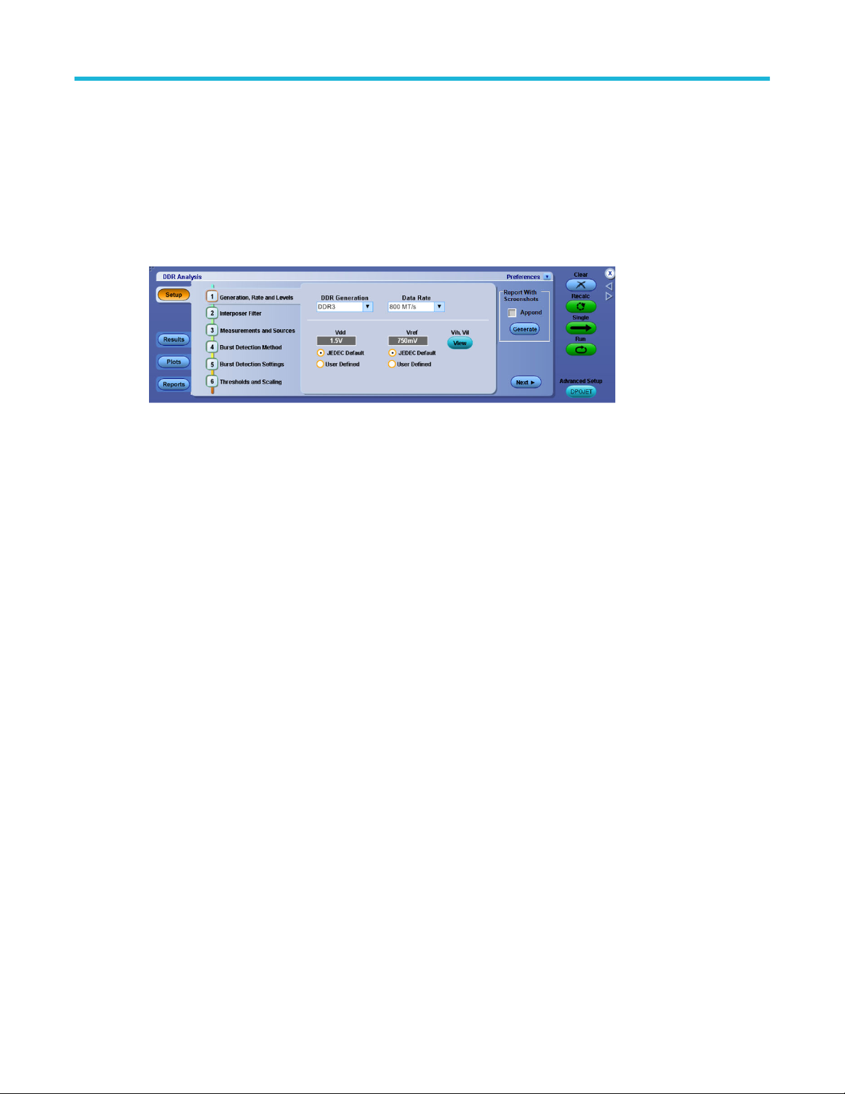
Welcome
DDR (Dual Data Rate) is a dominant and fast-growing memory technology. It offers the high data transfer rates needed for
virtually all computing applications, from consumer products to the most powerful servers. The high speeds of these signals
require high performance measurement tools.
The DDRA application includes compliance measurements as part of the Tektronix DDR Analysis solution. The DDR
Analysis solution enables you to achieve new levels of productivity, efficiency, and measurement reliability. It requires the
Jitter and Eye Diagram Analysis tool (Opt. DJA) and the Advanced Search and Mark capability (Opt. ASM).
Some of the DDRA features are:
• Provides debug, analysis, and compliance in one solution for multiple DDR standards such as DDR, DDR2, DDR3,
• Enables analysis of compliance measurements either through the DDRA or DPOJET application for all bursts in an
• Differentiates data reads from writes or analyzes signal integrity on the clock or on a data (DQ) line during Read or Write
• Includes limit files to test measurement pass/fail status per standard, speed grades and speed bins. Supports non-
• Provides both single-ended and differential measurements on Data, Strobe, Clock, Address and Command signals.
• Includes comprehensive measurement statistics.
• Includes sophisticated graphical analysis tools such as Histograms, Time Trends, Spectrums, Bathtub Plots, and Real-
• Produces consolidated reports automatically with pass/fail information, statistical measurement results, setup
• Automatically applies signal slew rate derating of measurement limits for Address/Command and data signals.
• Dynamically normalizes limits for clock measurements such as tERR based on the measured tCK(avg).
• Logic state configuration using the DDRA user interface.
Welcome
DDR3L, DDR4, LPDDR, LPDDR2, LPDDR3, LPDDR4, LPDDR4X, GDDR3, and GDDR5.
acquisition.
cycles, or measures Data to Strobe setup and hold during Write cycles.
standard speed grades.
Time Eye® diagrams with superimposition of the strobe eye with the data eye.
information, limits information, waveform path location, plots, and user comments, if any.
DDR
DDR is the DRAM (Dynamic Random Access Memory) technology responsible for increasing data transfer rates to meet
high-speed requirements and data capacity of computer systems.
DDR2
DDR2 is the Double Data Rate 2 SDRAM (Synchronous Dynamic Random Access Memory) and is widely available in
products with data rates up to 1066 MT/s.
DDR3
DDR3 DRAM memory is widely available in products and extends data rates to 1600 MT/s and faster rates to come.
DDR Analysis Memory Interface Electrical Verification and Debug Solution Printable Application Help xv
Page 16

Welcome
DDR3L
DDR3L (Low voltage) DRAM memory is widely available in products and extends data rates to 1600 MT/s and faster rates
to come.
DDR4
DDR4 DRAM memory is widely available in products and extends data rates to 3200 MT/s and faster rates to come.
LPDDR
LPDDR (Low Power DDR) is a technology for mobile phones and portable computing devices, driven by the need for faster
operation with long battery life.
LPDDR2
LPDDR2 (Low Power DDR2) is a technology for mobile phones and portable computing devices as it supports advanced
power management. It includes a reduced interface voltage of 1.2 V from the 1.8 V specification as compared to LPDDR
memory technology. This results in a power consumption reduced by over 50%.
LPDDR3
LPDDR3 (Low Power DDR3) is a technology for mobile phones and portable computing devices as it supports advanced
power management. It includes a reduced interface voltage of 1.2 V from the 1.8 V specification as compared to LPDDR
memory technology. This results in a power consumption reduced by over 50%.
LPDDR4
LPDDR4 (Low Power DDR4) is an emerging technology for mobile phones and portable computing devices as it supports
advanced power management. It includes a reduced interface voltage of 1.1 V from the 1.8 V specification as compared to
LPDDR memory technology.
LPDDR4X
LPDDR4X (Low Power DDR4X) is an extension to the LPDDR4 standard. It is identical to LPDDR4, except that additional
power is saved by reducing the I/O voltage (Vddq) to 0.6 V rather than 1.1 V.
GDDR3
GDDR3 (Graphic DDR3) offers faster access and is used in graphics-intensive applications such as video cards and gaming
systems.
GDDR5
GDDR5 (Graphic DDR5) is a type of high performance dynamic random-access graphics card memory designed for
applications requiring high bandwidth.
DDR Analysis Memory Interface Electrical Verification and Debug Solution Printable Application Help xvi
Page 17

Introduction
Related documentation
Tektronix manuals and softwares are available at: www.tektronix.com/manuals and www.tektronix.com/software. Use the
following table to determine the document that you need:
Table 1: List of reference documents
For information on Refer to
• Operating the oscilloscope Refer to the documentation for your oscilloscope.
Introduction
• Software warranty
• List of available applications
• Compatible oscilloscopes
• Relevant software and firmware version numbers
• Applying a new option key label
• Installing an application
• Enabling an application
• Downloading updates from the Tektronix Web site
Conventions
This online help uses the following conventions:
• When steps require a sequence of selections using the application interface, the > delimiter marks each transition
• The terms DDR application and application refer to DDRA.
• The term DPOJET application or DPOJET refers to the Jitter and Eye Diagram Analysis Tool.
• The term oscilloscope refers to any product on which this application runs.
• The term DUT is an abbreviation for Device Under Test.
For details, refer to Optional Applications Software on
Windows-Based Oscilloscopes Installation Manual.
between a menu and an option. For example, Analyze > DDR Analysis.
• User interface screen graphics are taken from a DPO7000 series oscilloscope.
Technical support
Tektronix welcomes your comments about products and services. Contact Tektronix through e-mail, telephone, or the Web
site. Click www.tektronix.com/manuals for more information. Tektronix also welcomes your feedback. Click Customer
feedback for suggestions for providing feedback to Tektronix.
Customer feedback
Tektronix values your feedback on our products. To help us serve you better, please send us your suggestions, ideas, or
other comments you may have regarding the application or oscilloscope.
Direct your feedback through e-mail to
techsupport@tektronix.com
DDR Analysis Memory Interface Electrical Verification and Debug Solution Printable Application Help 1
Page 18

Introduction
Or FAX at (503) 627-5695, and include the following information:
General Information
• Oscilloscope series (for example: DPO7000C or DSA/DPO/MSO70000C/D/DX series) and hardware options, if any
• Software version number
• Probes used
Application-specific Information
• Description of the problem such that technical support can duplicate the problem
• If possible, save the oscilloscope and application setup files as .set and associated .xml files.
• If possible, save the waveform on which you are performing the measurement as a .wfm file.
Once you have gathered this information, you can contact technical support by phone or through e-mail. In the subject field,
please indicate DDRA Problem and attach the .set, .xml and .wfm files to your e-mail. If there is any query related to
the actual measurement results, then you can generate a .mht report and send it. If you need to send very large files,
technical support can assist you to transfer the files through ftp.
The following items are important, but optional:
• Your name
• Your company
• Your mailing address
• Your phone number
• Your FAX number
Enter your suggestion. Please be as specific as possible.
Please indicate if you would like to be contacted by Tektronix regarding your suggestion or comments.
DDR Analysis Memory Interface Electrical Verification and Debug Solution Printable Application Help 2
Page 19

Getting started
DDRA prerequisites
DDRA application requires DPOJET Advanced (Opt. DJA) and Search and Mark (Opt. ASM) to be enabled.
Requirements and restrictions
DPOJET (DJA) is required to operate DDRA on your oscilloscope. Also refer to subsequent requirements for DPOJET.
Supported probes
The application supports the following probes:
• TAP2500
• TAP1500
• TCP0030
• P6158
• P6101B
• P6246
• P6247 (DPO7254 only)
• P6248 (DPO7254 only)
• P6249
• P6150
• P6158
• P7240
• P7260
• P7330
• P7340A
• P7350
• P7360A
• P7380A
• P7313A
• P7513
• P7520A
• P7520
• P7500 Series TriMode Probes
• P7700 Series TriMode Probes
Getting started
Installing the application
Refer to the Optional Application Software on Windows-Based Oscilloscopes Installation Manual for the following
information:
• Software warranty.
• List of available applications, compatible oscilloscopes, and relevant software and firmware version numbers.
• Applying a new option installation key label.
• Installing an application.
• Enabling an application.
• Downloading updates from the Tektronix Web site.
DDR Analysis Memory Interface Electrical Verification and Debug Solution Printable Application Help 3
Page 20
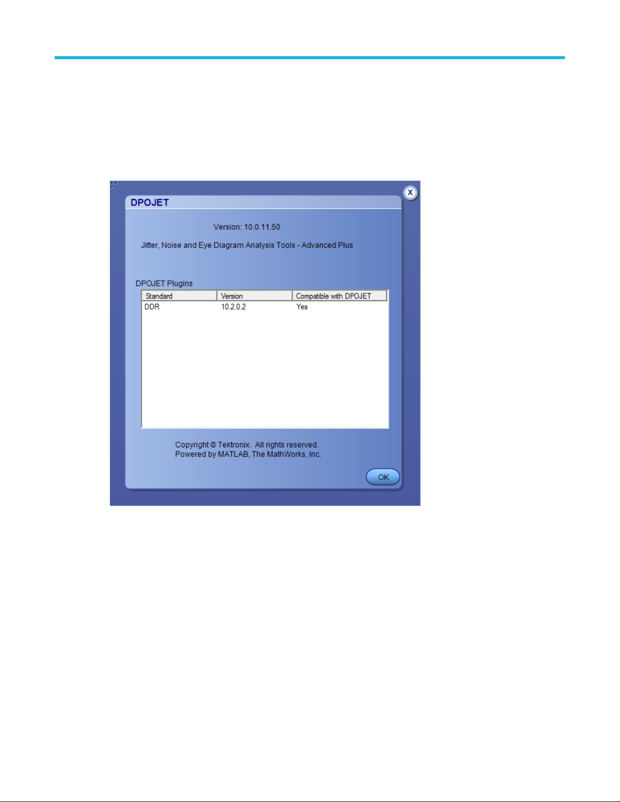
For DDRA application, install both DPOJET and DDRA after re-installing TekScope. The sequence that should be followed:
• TekScope
• DPOJET
• DDRA
Version information
To identify the installed version of the DDRA application, click Help > About DPOJET.
Getting started
DDR Analysis Memory Interface Electrical Verification and Debug Solution Printable Application Help 4
Page 21

Tutorial
Introduction to the tutorial
This tutorial shows how to set up the application, take measurements, and view results as plots or statistics.
Before you begin the tutorial, perform the following tasks:
• Set up the oscilloscope.
• Start the application.
• Recall the tutorial waveform.
Setting up the oscilloscope
The steps to set up the oscilloscope are:
• Click File > Recall Default Setup in the oscilloscope menu bar to recall the default settings.
• Press the individual CH1, CH2, CH3, and CH4 buttons as needed to add or remove active waveforms from the display.
Starting the application
Tutorial
On the oscilloscope menu bar, click Analyze > DDR Analysis to open the application.
Waveform files
The DDRA application provides the following waveforms at C:\Users\Public\Tektronix
\TekApplications\DDRA\Waveforms\DDR2 for oscilloscopes running the Windows10 operating system:
• DDR2_800_DQS_Write.wfm
• DDR2_800_DQ_Write.wfm
• DDR2_800_CLK.wfm
Note: These waveforms have to be used only for Write bursts and CLK.
Recalling a waveform file
To recall a waveform file, follow these steps:
1. Click File > Recall in the oscilloscope menu bar to display the Recall dialog box.
2. Click Waveform icon in the left of the Recall dialog box.
3. Select Ref1, Ref2, Ref3, or Ref4 as the Destination option.
4. Browse to select the waveform. Use the keypad to edit the waveform file name.
5. Click Recall.
The oscilloscope recalls and activates the Reference Waveform control window.
6. Click On to display the waveform.
7. Click to return to the application. Alternatively, DDRA can also be accessed from Analyze > DDR Analysis.
DDR Analysis Memory Interface Electrical Verification and Debug Solution Printable Application Help 5
Page 22
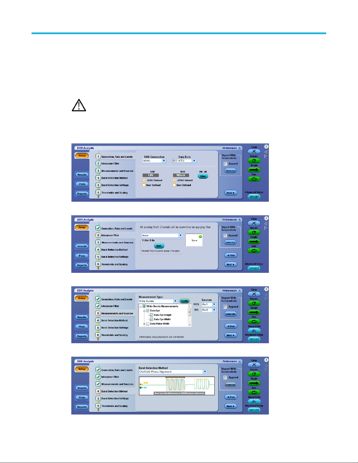
Taking a measurement
This tutorial uses the following example:
DDR2 800MT/s, Write bursts - Differential measurements
Waveforms Used: DDR2_800_DQS_Write.wfm and DDR2_800_DQ_Write.wfm
1. To set the application to default values, click File > Recall Default Setup.
Note: This is not necessary if you have just started the application.
2. To view the DDRA application, select Analyze > DDR Analysis.
3. At Step 1, select the DDR2 standard and the data rate as 800 MT/s.
The default voltage settings are retained as shown.
Tutorial
4. At Step 2, select the filter.
5. At Step 3, select the measurements and the associated sources.
6. At Step 4, select the burst detection method.
DDR Analysis Memory Interface Electrical Verification and Debug Solution Printable Application Help 6
Page 23
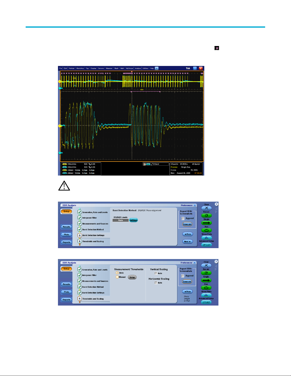
Tutorial
The selected data rate, generation, and measurement type are reflected in ASM (Advanced Search and Mark) on
selection in DDRA. Marks are available only for Read and Write bursts measurement type. Configure Search using
Analyze > Search > Configure. The identified bursts are shown as small inverted marks ( ) in the oscilloscope
display area. Each pair of marks specifies the start and stop of a burst. You can traverse from one mark to the other
using the Mark Control window. For more details, refer to Oscilloscope help.
Note: Logic state+ DQ/DQS Phase Alignment is available only for the MSO series of oscilloscopes.
7. At Step 5, configure the burst detection settings based on the selected burst detection method as shown.
8. At Step 6, retain the settings as shown.
9. Click Single to run the application.
When complete, the result statistics with limits are shown under the Results tab.
DDR Analysis Memory Interface Electrical Verification and Debug Solution Printable Application Help 7
Page 24
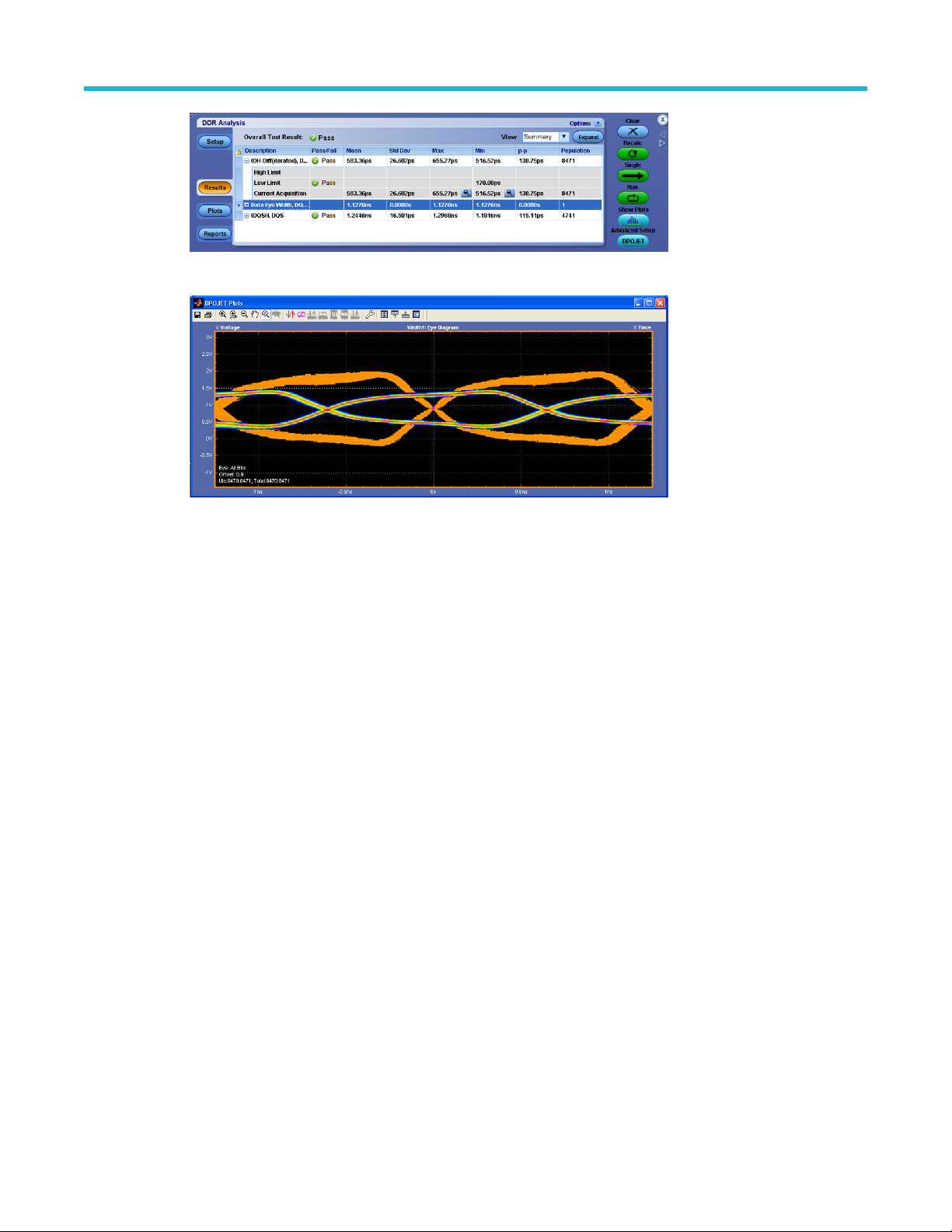
The eye diagram plot is displayed as shown.
Tutorial
DDR Analysis Memory Interface Electrical Verification and Debug Solution Printable Application Help 8
Page 25
Operating basics
About basic operations
DDRA user interface
Following are the description of DDRA user interface:
Operating basics
• Use the Single button
button again before process is completed will interrupt the processing cycle.
• Use the Run button to continuously acquire and accumulate measurements.
If prior measurements have been acquired and have not been cleared, the new measurements are added to the existing
set. Push the button again to interrupt the current acquisition.
• Use the Recalc button to perform measurements on the waveform currently displayed on the oscilloscope
without performing a new acquisition.
This is useful to modify a configuration parameter and re-run the measurements on the current waveform.
• Use the Clear button to clear all existing measurement results.
Note: Adding or deleting a measurement, or changing a configuration parameter of an existing measurement,
will also cause measurements to be cleared. This is to prevent the accumulation of measurement statistics or
sets of statistics that are not coherent.
Basic oscilloscope functions
Application directories
During DDRA application installation, various folders are created as described in the following table.
Type Directory path Description
Application
executables
Limits
Mask File
Symbol Files
C:\Program Files\TekApplications\DDRA
C:\Users\Public\Tektronix\TekApplications
\DDRA\Limits
C:\Users\Public\Tektronix\TekApplications
\DDRA\Masks
C:\Users\Public\Tektronix\TekScope
\BusDecodeTables\DDR
to obtain a set of measurements from a single new waveform acquisition. Pushing the
Contains DDRA application
assembly files.
Contains limit files of DDRA
standards and speed grades.
Contains mask files used for eye
measurements.
Contains symbol files.
File name extensions
Table 2: File name extensions
File Extension Description
.csv
Table continued…
DDR Analysis Memory Interface Electrical Verification and Debug Solution Printable Application Help 9
An ASCII file containing Comma Separated Values. This file format may be read by any
ascii text editor (such as Notepad) or may be imported into spreadsheets such as Excel.
Page 26
File Extension Description
Operating basics
.xml
.set
.mht
.wfm
.tsf
Returning to the application
When you access oscilloscope functions, the DDRA control windows may be replaced by the oscilloscope control windows
or by the oscilloscope graticule. You can access oscilloscope functions in the following ways:
• From the menu bar on the oscilloscope, choose Analyze > DDR Analysis.
• Alternatively, you can switch between recently used control panels using the forward or back arrows on the
right corner of the control panel.
Control panel
The Control panel appears on the right side of the application window. Using this panel, you can start or stop the sequence
of processes for the application and the oscilloscope to acquire information from the waveform. The controls are Clear,
Recall, Single, and Run. The following table describes each of these controls:
An ASCII file containing measurement setup information, limits or other data in Extensible
Markup Language.
A binary file containing oscilloscope setup information in a proprietary format.
An HTML archive file, compatible with common Windows applications; contains the full
report, including text and graphics.
A binary file containing an oscilloscope waveform record in a recallable, proprietary format.
A symbol file containing various symbols for various logic trigger patterns.
Item Description
Clear Clears the current result display and resets any statistical results and autoset reference
levels. For any input sources that have reference level autoset enabled, this control clears
the current reference levels so that they will be recalculated during the next acquisition.
Recall Runs the selected measurements on the currently displayed waveform(s), without first
performing a new acquisition.
Single Initiates a single new acquisition and runs the selected measurements.
Run Initiates new acquisitions and runs the selected measurements repeatedly until Stop is
selected. For any non-live sources (Reference waveforms or Math waveforms not
dependent on a live channel), only a single processing cycle will occur.
Show Plots Displays the Plot summary window when selected. This button appears in the control panel
only when one or more plots have been defined.
Advanced Setup DPOJET Transitions to the Jitter and Eye Diagram Analysis application when selected, importing all
currently defined DDRA measurements. This button appears in the control panel when you
open the DDR analysis application. This is useful to add additional measurements not
defined in DDRA, or to change measurement configurations to intentionally deviate from
those recommended by DDRA.
DDR Analysis Memory Interface Electrical Verification and Debug Solution Printable Application Help 10
Page 27
Saving and recalling setups
Saving a setup
The DDRA application state is automatically saved along with the oscilloscope state. To save the oscilloscope settings and
the application state, do the follow steps:
1. Click File > Save As > Setup.
2. In the file browser, select the directory to save the setup file.
3. Select or enter a file name.
The application appends *_DDRA.xml and *_DPOJET.xml to store the DDR setup, and *.set to store the
oscilloscope settings.
4. Click Save.
Note: After the oscilloscope application is started, DDRA needs to be launched at least once before any saved
DDRA configuration can be recalled.
Recalling a saved setup
To recall a previously saved set of application and oscilloscope settings, do the following steps:
Note: While recalling setup files with both DDRA and DPOJET saved settings, DDRA setup values get a higher
precedence over DPOJET setup values. For example, select a DPOJET measurement and a DDRA measurement,
change the ref levels of DPOJET measurement, and save the setup file. On recalling the setup file, you will see
that the DPOJET reference level settings are overwritten by the DDRA measurement ref levels.
Operating basics
1. Click File > Recall.
2. Click Setup in the left column if it is not already selected.
3. Select the directory in the file browser to recall the setup file.
4. Select a .set file and click Recall.
Note: If DDRA has been launched at least once since the oscilloscope application was started, only .set files can
be selected. Also, any corresponding *_DDRA.xml and *_DPOJET.xml files in the same directory will be recalled as
well but the DDRA configuration will be ignored.
Recalling the default setup
To recall the default application and oscilloscope settings, click File > Recall Default Setup.
Note: Recalling the default setup sets the DDRA application to DDR3 generation and the data rate to None.
Search and mark
The data rate, generation, and measurement type selected in DDRA are also set in Advanced Search and Mark (ASM).
Marks are available only for the Read and Write bursts measurement types. You can configure Search using Analyze >
Search > Configure. The identified bursts are shown as small inverted marks ( ) in the oscilloscope display area. Each
pair of marks specifies the start and stop of a burst. You can move from one mark to the other using the Mark Control
window.
Note: LPDDR4/LPDDR4X burst cannot be configured from ASM window.
DDR Analysis Memory Interface Electrical Verification and Debug Solution Printable Application Help 11
Page 28
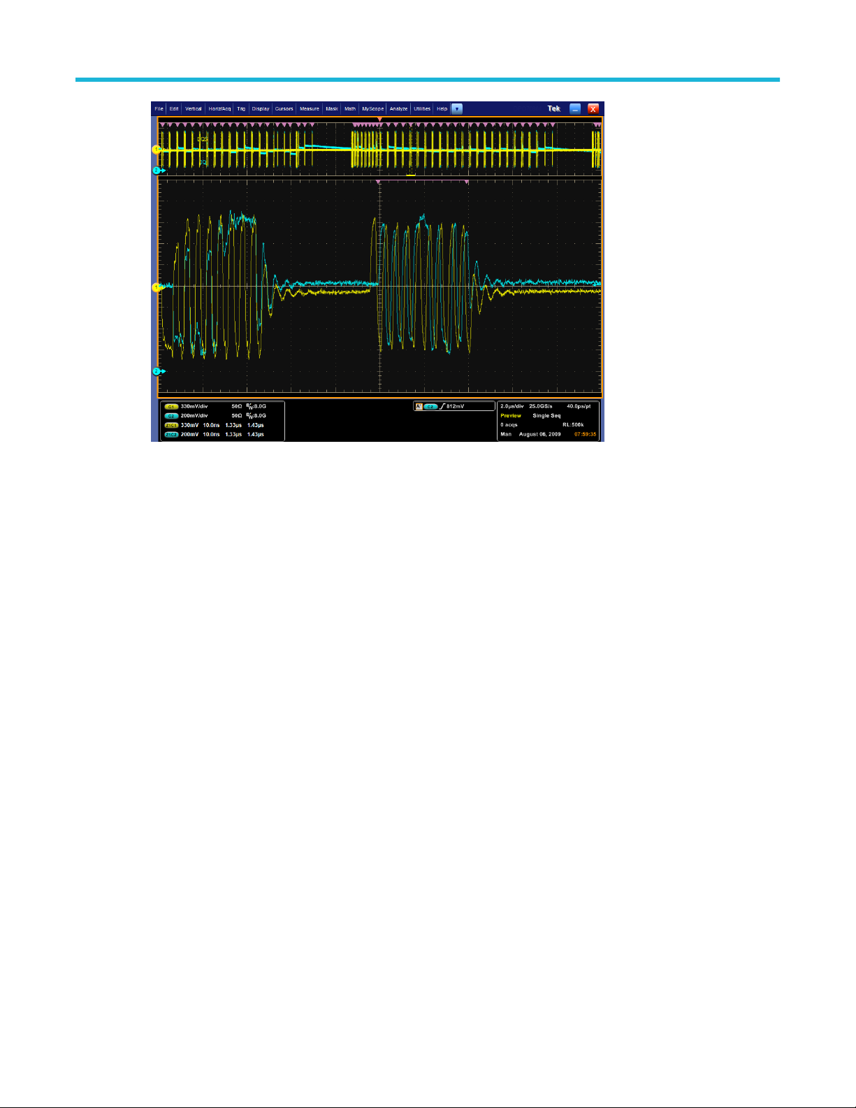
Operating basics
Limits
A limits file allows you to configure the limits used to determine the Pass or Fail status for tests. Each limits file includes a
list of one or more measurements, and the ranges of acceptable values for any or all statistics for each measurement. The
measurement include combinations of all measurements and statistical characteristics, and an appropriate range of values
for each combination.
The application provides preconfigured limits files for many combinations of standards and speed grades. You can create a
limit file by specifying limits for any of the result parameters such as Mean, Std Dev, Max, Min, peak-to-peak, population,
MaxPosDelta, and MinPosDelta. For each of these result parameters, you can specify the Upper Limit Equality (UL), and
the Lower Limit Equality (LL). The measurement names in the limits file must be entered as mentioned in About DDR
Analysis.
To include pass/fail status in the result statistics, you can create a custom limits file in the following format using an XML
editor or any other editor. If the file is created in any other editor such as Notepad, it should be saved in Unicode format.
The following is a sample of the limit file for DDR2 generation, the data rate being 667 MHz -
DDR2_667MHz_Limits.xml
<?xml version="1.0" encoding="utf-8"?>
<Main>
<!-- DDR2 667MHz Limits -->
<Measurement>
<NAME>tDH-Diff(base)</NAME>
<STATS>
<STATS_NAME>Min</STATS_NAME>
<LIMIT>LL</LIMIT>
<UL>0</UL>
<LL>175e-12</LL>
</STATS>
</Measurement>
<Measurement>
<NAME>tDS-Diff(base)</NAME>
DDR Analysis Memory Interface Electrical Verification and Debug Solution Printable Application Help 12
Page 29
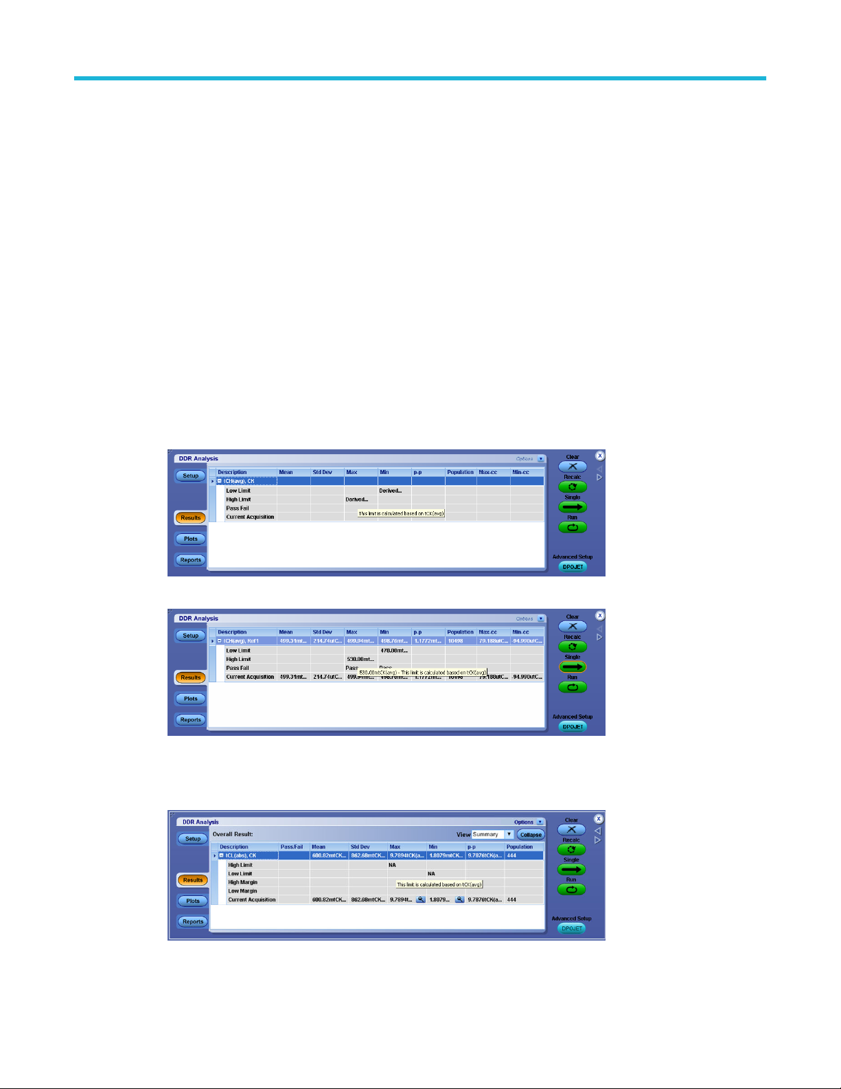
You can find limit files for various data rates of different DDR standards and speed bins at C:\Users\Public
\Tektronix\TekApplications\DDRA\Limits.
Dynamic limits
The application supports both static (predefined, using limits file) and dynamic limits.
The concept of dynamic limits is explained taking an example of a measurement, tCH(avg):
• If the dynamic limits of a measurement depend on the result of other measurement(s) that have not yet been calculated,
the limit field in the Results panel shows Derived... A tool tip displays the message:
This limit is calculated based on measurement tCK(avg).
Operating basics
<STATS>
<STATS_NAME>Min</STATS_NAME>
<LIMIT>LL</LIMIT>
<UL>0</UL>
<LL>100e-12</LL>
</STATS>
</Measurement>
</Main>
• On clicking Run/Single, the results are shown in the following figure.
• If there is an error in calculating dynamic limits or if the limits are not defined by the specification, the limit text field
displayed NA. A tool tip displays the message:
This limit is calculated based on measurement tCK(avg).
DDR Analysis Memory Interface Electrical Verification and Debug Solution Printable Application Help 13
Page 30
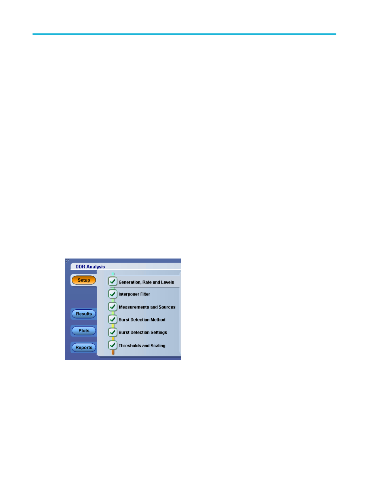
Log messages
Dynamic limit failure:
1. The limits for measurement is not defined in the JEDEC specification.
2. The limits for measurement cannot be computed due to unavailability of dependent measurement results.
References
Dynamic Limits for DDR Measurements
Dynamic Limits for DDR2 Measurements
Dynamic Limits for DDR3 Measurements
Dynamic Limits for DDR3L Measurements
Dynamic Limits for DDR4 Measurements
Dynamic Limits for LPDDR Measurements
Dynamic Limits for LPDDR2 Measurements
Dynamic Limits for LPDDR4 Measurements
Dynamic Limits for LPDDR4X Measurements
Operating basics
Setting up DDR for analysis
About DDR analysis
The DDR Analysis window allows you to select various standards and to set up and run a pre-configured measurement
either through the DDRA or the DPOJET application.
Select Analyze > DDR Analysis to open the DDRA application.
The Setup panel in DDR Analysis application includes the following steps:
Generation, Rate and Levels
Interposer Filter
Measurements and Sources
Burst Detection Method
Burst Detection Settings
DDR Analysis Memory Interface Electrical Verification and Debug Solution Printable Application Help 14
Page 31

Operating basics
Thresholds and Scaling
Note: Use the Next/Prev buttons or click directly on the step numbers to move through the steps in the DDR
Analysis. The steps for which configuration is complete are denoted.
The Setup panel displays hints to help you understand the configuration options wherever applicable.
You can run a set of measurement in either of the two ways:
• Click Run to start the acquisition sequence using the selected settings and to view the results in the DDRA window. This
is the normal way to generate results.
• Click
For more details, refer to the DPOJET help.
• Click in the DPOJET application to return to the DDRA window. Alternatively, you can reselect Analyze >DDR
Analysis from the menu bar.
to move to the DPOJET application where you can add or modify measurements before sequencing.
Step 1: Generation rate and levels
Select the DDR generation, data rate, and the voltage levels (if required).
1. Select the generation from the DDR Generation drop-down list.
2. Select the data rate from the Data Rate drop-down list.
On selecting Custom, an edit box allows you to enter the value using the virtual keypad. Limit files are not defined for
custom data rates for pass/fail status and as a result, the application displays a hint at the bottom of the screen:
Please provide a limits file under Jitter and Eye Analysis > Limits.
Note: Selecting Auto data rates in ASM (under Search > DDR Read or DDR Write) changes the data rate to
None in DDRA.
3. Set the voltage levels:
• If you select JEDEC defaults, the application uses the nominal voltage levels according to the JEDEC specification.
The Vdd field is not editable.
• If you select User Defined, enter the Vdd or Vref voltage values using the virtual keypad.
Note: The Vcent_DQ and Vcent_CA voltage values are only available for DDR4, LPDDR4, and LPDDR4X.
For these generations, the external Vref is not available. Vcent is similar to the traditional Vref parameter
but takes into account the actual reference voltage used inside the DRAM is adjusted during write training
and is not physically visible at the balls of the DRAM.
4. (Optional) Click View to view the Vih and Vil values calculated automatically based on the Vref value. To manually adjust
the reference levels, go to Step6 of DDRA or use the DPOJET source configuration panel.
Vdd Vdd is the supply voltage for each DDR standard. Vdd is based on DDR generation.
Table continued…
DDR Analysis Memory Interface Electrical Verification and Debug Solution Printable Application Help 15
Page 32

Operating basics
Vref Vref is the reference voltage for each DDR standard. Vref is calculated using Vdd, which is based on DDR
generation. In most cases, Vref=0.5 Vdd.
Vcent
Vcent_DQ is the voltage at which the cumulative eye of the pin DQx is widest.
_DQ
Vcent
Vcent_CA is the voltage at which the cumulative eye of the pin CAx is widest.
_CA
VOH VOH is the output voltage swing for LPDDR4 and LPDDR4X.
In LPDDR4, VOH = V
In LPDDR4X, VOH = V
DDQ
DDQ
/2.5 or V
/1.66 or V
/3 (Default)
DDQ
DDQ
/2 (Default)
VDDQ VDDQ is the voltage internally applied to the I/O buffer.
In LPDDR4X, VDDQ is set to the nominal voltage of 0.6 V. In other generations, VDDQ is set to VDD
The following table lists the minimum and maximum values of Vdd, Vref, Vcent_DQ, and Vcent_CA in the User
Defined mode for all DDR generations:
1
DDR
DDR2 DDR3 DDR3LDDR4 LPDDRLPDDR2LPDDR3LPDDR4LPDD
GDDR3GDDR
R4X
Vdd Default 2.5V 1.8V 1.5V 1.35V 1.2V 1.8V 1.2V 1.2V 1.1V 1.1V 1.8 V 1.5V
Range -6 to 6V
Vref Default 1.25V 900mV 750mV 675mV 900mV 600mV 600mV 900mV 750mV
Range -6 to 6V -6 to 6V -6 to 6V
Vcent_DQDefault
Range -2V to
Vcent_CADefault
Range -2V to
850mV
2V
600mV
2V
201.5
150mV
mV
0V to 2.5V
191.5mV301.8
mV
0V to 2.5V
VDDQ Default 600mV
Range 0V to
5V
VOH Default VDDQ/3VDDQ/
2
Option
s
For LPDDR4X VOH = { VDDQ/2, VDDQ/1.66 }
For LPDDR4 VOH = { VDDQ/3, VDDQ/2.5 }
5
Vdd and Vref
The configured values of Vdd and Vref are used to calculate V
applied on the input signal. These levels are further used for calculating Setup and Hold measurements.
For DDR2, the relationship between Vdd and Vref is as shown in the following tables:
1
DDR 400 MT/s has Vdd value set to 2.6 V and Vref Value set to 1.3 V
DDR Analysis Memory Interface Electrical Verification and Debug Solution Printable Application Help 16
IH(ac)
min, V
IH(dc)
min, V
max, and V
IL(dc)
max which are
IL(ac)
Page 33

Table 3: Input DC logic level
Symbol Parameter Min Max Units
Operating basics
V
V
IH(dc)
IL(dc)
DC input logic high Vref+0.125 NA V
DC input logic low –0.3 Vref–0.125 V
Table 4: Input AC logic level
Symbol Parameter DDR2–400, DDR2–533 DDR2–667, DDR2–800 Units
Min Max Min Max
V
IH(ac)
V
IL(ac)
Note: Similar reference voltage levels are defined for the DDR3 standard.
AC input logic
high
AC input logic
low
Vref+0.250 NA Vref+0.200 NA V
NA Vref–0.250 – Vref+0.200 V
Speed Bins
For each DDR standard, the DDRA application automatically applies limits appropriate for the standard data rates without
speed bins. Limit values are different for different speed bins. If you want to test according to a speed bin, you must
manually configure the limit values from within DPOJET by manually overriding the limit file before running the
measurements. For more details, refer to Limits in the DPOJET help.
Vih
Vih is the input logic HIGH voltage.
Vil
Vil is the input logic LOW voltage.
Step 2: Interposer filter
Allows you to select and apply the interposer type for each of the sources. Filter.xml file is available at C:\Users
\Public\Filters. This file can be edited to add different interposer types. The absolute filter path for each source
can be specified. You can specify filter files either for all the available sources or only to a subset of sources. Select the
appropriate interposer de-embedding filter files before selecting the measurements. It is recommended to do the horizontal
autoset before applying any interposer filter files.
When interposer filters are applied, MATH cannot be used as the measurement source in Step 3. It is recommended to
manually clear all Math expressions before applying any interposer filters through DDRA. The filter file is applied when the
scope acquisition sample rate is supported in the filter file. Math channels get enabled only if the scope sampling rate
matches with the sampling rate of the de-embedding filter; otherwise, Math will not be enabled and measurements will not
be executed.
Note: The fields and options on the Interposer filter tab appears based on the type of generation selected. The
DDRA supports the de-embedding of interposers with live signals only.
DDR Analysis Memory Interface Electrical Verification and Debug Solution Printable Application Help 17
Page 34

Operating basics
Filter types
• None: Select if you do not to want to apply filter files. This option is selected by default.
• Direct Attached: Select to attach pre-defined filter files.
• User Defined: Select to define a pre-defined filter files. If you do not define at least one filter for a source, then after
clicking the Close button, the Interposer selection defaults to None.
Note: Interposer types such as None, Direct Attached, and User Defined are embedded in the application.
You can add additional filter files by adding the filter file name to the Filter.xml file. Once you update the XML file, restart the
TekScope to apply the changes. The names you added are now referenced in the Interposer filter type drop-down list.
Note: If filter files do not exist or there is any typo in entering the path, the application displays a message
Filter File does not exist for <source name> in the path specified. The
list of sources for which the filter files are not found will be listed.
Edit button: Opens the Filter.xml file for editing.
User define filter path
When you select User Defined from the drop-down list, User Defined text is auto populated on the
image box to view the User Defined Filter Path dialog box, and then select different filer files for each source by clicking the
Browse button. You can remove the selected filter file path by clicking the Clear button or click the Clear All button to clear
all the filer paths at once.
image box .Click the
DDR Analysis Memory Interface Electrical Verification and Debug Solution Printable Application Help 18
Page 35

Operating basics
Note: The source displayed in User Defined Filter Path dialog box shall be enabled or disabled based on selected
generation. Filter files can be selected for subset or all of the available sources. The Filters.xml file is located at
C:\Users\Public\Filters folder. The filter file can also be modified outside the application.
Step3: Measurements and sources
Select measurements and their corresponding Sources in this step. Measurement availability depends on the selected DDR
standard. Select the Measurement Type (Read Bursts, Write Bursts, Clock(Diff), Clock(Single Ended), DQS(Single Ended,
Write), DQS(Single Ended, Read), Address/Command, Overshoot and Undershoot, WCK(Single Ended), WCK(Diff),
Refresh, Power Down, Active, Precharge) from the drop-down list. Power Down, Active, Precharge, Refresh types are
available only on MSO models. A message prompts you to select one or more measurements before moving to the next
step.
Measurement Type Reference Levels
The voltage reference levels for each measurement are automatically set to be consistent with JEDEC guidelines unless
they are manually overridden. In cases where none of the chosen measurements have any applicable guidelines or
manually set levels, DDRA will automatically choose reference levels based on the signal's maximum and minimum levels.
DDRA displays a hint if both Single Ended DQS and Differential DQS measurements are selected at the same time, and
measurements made with this configuration may not be accurate due to conflicting ref level requirements. When two or
DDR Analysis Memory Interface Electrical Verification and Debug Solution Printable Application Help 19
Page 36

Operating basics
more measurements are selected in different sub-node categories under a Measurement Type, the following precedence is
set for measurement ref levels:
• Slew Rate ref levels
• Single Ended specific ref levels
• Differential specific ref levels
For Example, when Eye Width measurement is selected along with Differential DQS or Single Ended DQS or Slew Rate
measurements, Eye measurement may not produce the expected results. This is because the actual mid level needed by
Eye Width gets overwritten with SE levels and hence produces no results.
Tree Structure Flow
The measurement tree structure is as follows:
• The tree structure displays only those measurements appropriate for the selected measurement type.
• All generations display both parent and nested elements under measurement type as shown.
• Click to expand and show the elements within the parent element.
• Click to collapse and hide the elements within the parent element.
• Selecting the parent check box, selects all the children elements. Selecting all the children elements, selects the parent
element.
DDR Analysis Memory Interface Electrical Verification and Debug Solution Printable Application Help 20
Page 37

Operating basics
• Clearing the parent check box clears all the children elements.
• When the children include both checked and unchecked elements, the parent element becomes highlighted as shown:
Note: If you move to the next step without selecting any measurements, the application displays the message,
Please select measurements in Step3.
Timing Mode
Select either 1T or 2T depending on memory mode in which DUT are operating. Timing Mode is applicable for DDR3,
DDR3L, DDR4 generation Address/Command's Setup and hold measurements.
Mask Margin Measurement
You can specify a custom mask file using the Mask file control. The Mask file control allows you to change mask width,
mask height, and mask position. When Mask margin measurement is selected, the application will update the default mask
file depending on the data rate selected. You should not modify the default mask files.
DDR Analysis Memory Interface Electrical Verification and Debug Solution Printable Application Help 21
Page 38

Operating basics
Timing error (tERR) measurements
Timing error measurements such as tERR(02per), tERR(03per), tERR(09per) until tERR(50per) are grouped together and
included as a nested element (tERR) under the parent element, Clock(Diff)measurements. Selecting tERR selects all the
timing error measurements.
Sources
Select a measurement to view the sources available for the measurement. The sources are mutually exclusive. For each
required signal, select the appropriate source. A tool tip displays the required sources for the selected measurement at the
nodes of the measurement tree. A maximum of four analog sources are available at a time.
Note: If the same channels are used for DQ/DQS/Clock sources (Example: DQ=Ch1, DQS=Ch1), the application
displays a hint Cannot use the same waveform for different sources. If Live and Ref
channels are used together (Example: Ch1 for DQS and Ref2 for DQ), the application displays a hint Cannot
use Live and Ref waveforms together.
Reference
Hints
DDR Measurement Sources
DDR2 Measurement Sources
DDR3/DDR3L Measurement Sources
DDR4 Measurement Sources
GDDR5 Measurement Sources
LPDDR Measurement Sources
DDR Analysis Memory Interface Electrical Verification and Debug Solution Printable Application Help 22
Page 39

LPDDR2 Measurement Sources
LPDDR3 Measurement Sources
Measurement configurations
Clicking the Config button opens the Measurement Configurations dialog box, where you can configure various
measurement settings.
Available options:
• Select measurements as per reference level: Option to select only those measurements which have the common
sources/reference levels. The selected measurements are cleared when this option is toggled. By default, this option is
disabled. Selecting this option automates the selection of measurements which have common sources/reference levels
under a group and disables other measurements in that group whose sources/reference levels are different.
Operating basics
DDR3 sources/reference levels
The above concept is explained in the following table by taking an example of a measurement, Data Eye Height, of
DDR3 generation.
DDR Analysis Memory Interface Electrical Verification and Debug Solution Printable Application Help 23
Page 40

Table 5: Common source and reference levels of Data Eye Height measurement
Operating basics
Generation Measurem
ent type
DDR3 Write Burst
Measureme
nt
Measurement Sources Reference levels
Enabled Disabled DQS DQ Percentage Absolute
Write Burst Data Eye
Height
Data Eye
Width
Data Plus
Width
Data Slew
Rate
tDIPW-High Ch1 Ch2 Ch2
tDIPW-Low Ch1 Ch2 Ch2
Slew RateHoldFall(DQ)
Slew RateHoldRise(DQ)
Slew RateSetupFall(DQ)
Ch1 Ch2 Ch1
Ch2
Ch1 Ch2 Ch1
Ch2
Ch1 Ch2 Ch2
Ch1 Ch2 Ch2
Ch1 Ch2 Ch2
Slew RateSetupRise(DQ)
Differential
strobe
Differential
Input Level
Select DDR3 generation, and then select Write Burst measurement group and based on your selection, the application,
by default, considers the sources and reference levels of Data Eye Height measurement, as it falls first in the Write
tDQSH Ch1 Ch2 Ch1
tDQSL Ch1 Ch2 Ch1
tDQSS-Diff Ch1 Ch2 Ch1
tDSH-Diff Ch1 Ch2 Ch1
tDSS-Diff Ch1 Ch2 Ch1
tDVAC(DQ
S)
tWPRE Ch1 Ch2 Ch1
VIHdiff(AC) Ch1 Ch2 Ch1
VILdiff(AC) Ch1 Ch2 Ch1
Ch1 Ch2 Ch2
Ch1 Ch2 Ch1
DDR Analysis Memory Interface Electrical Verification and Debug Solution Printable Application Help 24
Page 41

Operating basics
Bursts measurement group and compare its sources/reference levels with that of other measurements which falls under
the Write Burst measurement group.
In the above table, it is shown that the Write Burst measurements and Differential strobe measurements are enabled
because the sources and reference levels of Data Eye Height measurement and Differential strobe measurements are
common, that is, the source of Data Eye Height and Differential strobe measurement are Ch1 and reference levels are
in Percentage. On the other hand, the measurements, Data Plus Width, Data Slew Rate, and Differential Input Level are
disabled because their sources and reference levels are not common with that of Data Eye Height measurement.
Effect of not selecting Select Measurements as per reference level option
When you select two or more measurements in a group, the measurement result varies as some measurements have
different sources/reference levels as compared to others and selecting all of them will affect the outcome of
measurement result. When you select two or more measurements under a group, the application, by default, considers
the sources and reference levels of the first measurement selected under that group only. The application compares the
sources and reference levels of the first measurement with that of other measurements of that group and if it finds that
there is any mismatch between the sources and reference levels of first measurement with that of other selected
measurements in that group, it displays a message as Measurement result may very as the Ref
levels are changed.
For example, first you select the InputSlew-Diff-Fall (DQS) and then select tWPRE from Write Burst measurement
group. Here the application considers the sources and reference levels of tWPRE measurement for measurement
results. As tWPRE measurement falls first in the Write Bursts measurement group, the application compares sources/
reference levels of tWPRE with that of InputSlew-Diff-Fall (DQS). If there is a mismatch, the application displays a
message as Measurement result may very as the Ref levels are changed.
Now, you have to manually verify and clear the selection of measurements of which sources and reference levels are
not common with that of tWPRE measurement.
Viewing the sources and reference levels
To view and verify the sources and reference levels of each measurement with that of tWPRE measurement, do the
following:
1. First, clear all the selected measurements, if you have selected them earlier from the DDR application, and then
select only tWPRE measurement.
2. Click
The DPOJET window appears.
button on the DDR application.
DDR Analysis Memory Interface Electrical Verification and Debug Solution Printable Application Help 25
Page 42

Operating basics
3. On the DPOJET window, click button.
The Source Configuration dialog box appears, showing the sources /reference levels of tWPRE measurement.
The Source Configuration dialog box shows the source of tWPRE measurement as Ch1 and reference levels (Level
Type) in percentage.
4. Navigate to the DDR application and clear the selection of tWPRE measurement from the group, and then select the
InputSlew-Diff-Fall (DQS).
Sources/reference levels of InputSlew-Diff-Fall (DQS)
DDR Analysis Memory Interface Electrical Verification and Debug Solution Printable Application Help 26
Page 43

Operating basics
5. Follow the above steps to verify the source and reference level of InputSlew-Diff-Fall (DQS).
The Source Configuration dialog box shows the source of InputSlew-Diff-Fall (DQS) as Ch1 and reference level
(Level Type) as Absolute. This means that the sources are common but the reference levels (Level Type) of both
measurements are different. As reference levels are not common, the measurement result will very. To pass the
results, clear the selection of InputSlew-Diff-Fall (DQS) form the group. Sometimes, the values (Rise and fall) will be
different (not common) then also the measurement result will vary.
Note: The same process applies when you select more than two or all measurements in a group or from
other groups.
• Measurements result unit as per JEDEC specification: Option to configure the measurements result unit as per
JEDEC specification. When disabled, time based measurement results will be in seconds. This option is enabled by
default.
• Show informative measurements: Select this option to show and hide informative measurements in the measurement
group as shown.
For example, select generation as DDR3, and then select Clock (Diff) measurement from the Measurement Type dropdown. The Informative measurements which are in Clock Eye group gets displayed when you select this option as
shown below.
DDR Analysis Memory Interface Electrical Verification and Debug Solution Printable Application Help 27
Page 44

Operating basics
When you clear this option, a message is displayed as Informative measurement are not shown.
Following table shows the list of informative measurements.
Table 6: Informative measurements
Generation Measurement Type Measurement
DDR Clock(Diff) Clock Eye Height (Informative)
Clock Eye Width (Informative)
DQS(Single Ended, Write) tDSH(DQS)(Informative)
tDSS(DQS)(Informative)
tDH(DQS)(Informative)
tDS(DQS)(Informative)
Vix(ac)DQS(Informative)
DDR2 Address/Command AddrCmd Eye Width(Informative)
Clock(Diff) Clock Eye Height (Informative)
Clock Eye Width (Informative)
DQS(Single Ended, Read) tDQSQ(DQS)(Informative)
DQS(Single Ended, Write) tDQSS(DQS)(Informative)
tDSH(DQS)(Informative)
tDSS(DQS)(Informative)
tDH(base)DQS(Informative)
tDH(derated)DQS(Informative)
tDS(base)DQS(Informative)
tDS(derated)DQS(Informative)
Table continued…
DDR Analysis Memory Interface Electrical Verification and Debug Solution Printable Application Help 28
Page 45

Operating basics
Generation Measurement Type Measurement
DDR3 Address/Command AddrCmd Eye Width(Informative)
tIH(max-derated)(Informative)
tIH(min-derated)(Informative)
tIS(max-derated)(Informative)
tIS(min-derated)(Informative)
Clock(Diff) Clock Eye Height (Informative)
Clock Eye Width (Informative)
DQS(Single Ended, Read) tDQSS(DQS)(Informative)
tDSH(DQS)(Informative)
tDSS(DQS)(Informative)
DQS(Single Ended, Write) tDQSS(DQS)(Informative)
tDSH(DQS)(Informative)
tDSS(DQS)(Informative)
Write Bursts tDH-Diff(max-derated)(Informative)
tDH-Diff(min-derated)(Informative)
tDS-Diff(max-derated)(Informative)
tDS-Diff(min-derated)(Informative)
DDR3L Address/Command AddrCmd Eye Width(Informative)
tIH(max-derated)(Informative)
tIH(min-derated)(Informative)
tIS(max-derated)(Informative)
tIS(min-derated)(Informative)
Clock(Diff) Clock Eye Height (Informative)
Clock Eye Width (Informative)
DQS(Single Ended, Read) tDQSS(DQS)(Informative)
tDSH(DQS)(Informative)
tDSS(DQS)(Informative)
DQS(Single Ended, Write) tDQSS(DQS)(Informative)
tDSH(DQS)(Informative)
tDSS(DQS)(Informative)
Write Bursts tDH-Diff(max-derated)(Informative)
tDH-Diff(min-derated)(Informative)
tDS-Diff(max-derated)(Informative)
tDS-Diff(min-derated)(Informative)
Table continued…
DDR Analysis Memory Interface Electrical Verification and Debug Solution Printable Application Help 29
Page 46

Operating basics
Generation Measurement Type Measurement
DDR4 Clock(Diff) Clock Eye Height (Informative)
Clock Eye Width (Informative)
tJIT(duty) Informative
DQS(Single Ended, Read) VSEH(DQS#)(Informative)
VSEH(DQS)(Informative)
VSEL(DQS#)(Informative)
VSEL(DQS)(Informative)
DQS(Single Ended, Write) VSEH(DQS#)(Informative)
VSEH(DQS)(Informative)
VSEL(DQS#)(Informative)
VSEL(DQS)(Informative)
Read Bursts tDVAC(DQS)(Informative)
Write Bursts tDVAC(DQS)(Informative)
GDDR3 Clock(Diff) Clock Eye Height (Informative)
Clock Eye Width (Informative)
GDDR5 Clock(Diff) Clock Eye Height (Informative)
Clock Eye Width (Informative)
LPDDR Clock(Diff) Clock Eye Height (Informative)
Clock Eye Width (Informative)
DQS(Single Ended, Write) tDSH(DQS)(Informative)
tDSS(DQS)(Informative)
tDH(DQS)(Informative)
tDS(DQS)(Informative)
LPDDR2 Address/Command tIH(max-derated)(Informative)
tIH(min-derated)(Informative)
tIS(max-derated)(Informative)
tIS(min-derated)(Informative)
Clock(Diff) Clock Eye Height (Informative)
Clock Eye Width (Informative)
Write Bursts tDH-Diff(max-derated)(Informative)
tDH-Diff(min-derated)(Informative)
tDS-Diff(max-derated)(Informative)
tDS-Diff(min-derated)(Informative)
LPDDR3 Clock(Diff) Clock Eye Height (Informative)
Clock Eye Width (Informative)
Table continued…
DDR Analysis Memory Interface Electrical Verification and Debug Solution Printable Application Help 30
Page 47

Operating basics
Generation Measurement Type Measurement
LPDDR4 / LPDDR4X Address/Command AutoFitRxMask(Informative)
Clock(Diff) Clock Eye Height (Informative)
Clock Eye Width (Informative)
VIHdiff(AC) Informative
VILdiff(AC) Informative
Clock(Single Ended) VSEH(CK#)(Informative)
VSEH(CK)(Informative)
VSEL(CK#)(Informative)
VSEL(CK)(Informative)
DQS(Single Ended, Write) VSEH(AC)DQS#(Informative)
VSEH(AC)DQS(Informative)
VSEL(AC)DQS#(Informative)
VSEL(AC)DQS(Informative)
Write Bursts AutoFitRxMask(Informative)
VILdiff(AC) Informative
VIHdiff(AC) Informative
• Enable back-to-back burst detection: Identifying the start and end of the burst is particularly difficult to perform during
a back-to-back burst, due to the missing preamble pattern in each sub bursts. In case of back-to-back bursts, the strobe
seems like one continuous long burst with/without bubble states. Examples of the back-to-back data burst are shown in
the following figures.
Note: The Back-to-Back Burst Detection method is applicable only for Chip Select, Latency + DQ/DQS Phase
Alignment measurements.
Both DQ/DQS Phase Alignment and Chip Select, Latency + DQ/DQS Phase Alignment burst detection methods identifies
Read and Write bursts based on the preamble and the phase relation that exist between DQ and DQS. However, in case of
back-to-back bursts, the preamble may or may not present for all the sub bursts. This makes it very difficult for the ASM
algorithm to separately identify and mark all the sub bursts within a back-to-back burst.
DDR Analysis Memory Interface Electrical Verification and Debug Solution Printable Application Help 31
Page 48

Operating basics
The Chip Select signal is used to identify the bubble states during a back-to-back burst and to mark the valid start bit of
each sub-burst within a continuous back-to-back burst. A few assumptions are used in this approach as follow:
1. Back-to-back burst data are applicable for only one rank at a time, that is, all the sub-bursts in a back-to-back burst are
only meant for one single rank/DIMM.
2. In a back-to-back burst, there will be only ONE bubble bit (if any) between any 2 consecutive sub-bursts.
3. All Chip Select transitions during a back-to-back burst, are related to either READ/WRITE data.
The below are the limitations of the algorithms:
1. Two bubble events is not supported.
2. The algorithm does not handle the conditions when another command (for example, PRECHARGE or REFRESH
command) happens in the midst of back-to-back bursts. When that happens, the chip select signal is asserted for two
clock cycles and therefore we cannot identify which of the two marks corresponds to the READ/WRITE command. In
such cases, all the data bits from that point onwards will be ignore.
3. Since in a back-to-back burst, all sub-bursts might not contain the preamble and postamble, it is recommended not to
execute measurements those are based on preamble and postamble region of the burst.
4. This feature is available only for DDR3, DDR3L and DDR4 generations.
How to configure CAS_min and CAS_Max
CAS_Max and CAS_min is measured from the CS transition corresponds to the READ/WRITE command to the driving
edge of the strobe. Configure CAS_Max and CAS_min in a such a way that both the transitions of the CS signal lie in
between. This is shown in the below diagrams.
DDR Analysis Memory Interface Electrical Verification and Debug Solution Printable Application Help 32
Page 49

Operating basics
Features
An option is provided in the Config panel (in Measurement and Sources panel) to enable or disable the back-to-back burst
algorithm. By default, this option will be disabled.
On enabling this option, the burst detection method will automatically change to Chip select, Latency + DQ/DQS Phase
Alignment. Similarly, either on generation change or on burst detection method change the back-to-back burst detection
option will get disabled.
The back-to-back burst detection option is applicable only for Read Bursts, Write Bursts, DQS(Single Ended, Write) and
DQS(Single Ended, Read) burst measurements.
Log messages
The following log messages are applicable for LPDDR4/LPDDR4X:
1. The computed tDQS2DQ value is -ve. Please enter the right tDQS2DQ value with UserDefined mode.
This message is logged when tDQS2DQ mode is auto and the measured tDQS2DQ value is -ve. In this case user has
to switch the tDQS2DQ mode to 'User defined' and manually key in the right tDQS2DQ value.
2. There is no Data transitions during the first bit. Please enter the right tDQS2DQ value with UserDefined mode.
This message is logged when there is no DQ transition in the first bit of the burst. In such cases the algorithm assumes
tDQS2DQ as half of the clock unit interval. So it is advised to switch the tDQS2DQ mode to 'User defined' and manually
key in the right tDQS2DQ value.
3. There are no isolated bursts in the acquisition. Either increase the record length or change the isolated burst
configuration.
This message is logged when there are no isolated bursts in the acquisition. In this case either:
a. Increase the record length which increases the possibility of acquiring a isolated burst.
b. Change the Isolated burst configuration.
c. Use a different burst identification method.
4. The configured postamble length may not be correct. Please check the configuration.
This message is logged when the acquired isolated Write burst has two extra UIs compared to the configured isolated
burst length.
5. The configured preamble type and/or postamble length may not be correct. Please check the configurations.
This message is logged when the acquired isolated Read burst has two or four extra UIs compared to the configured
isolated burst length.
6. Please configure the Burst Match(%) with a smaller value and try again.
This message is logged when the configured Burst match is higher than any burst' association index in the acquisition.
In this case it is advised to decrease the burst match value and try again.
DDR Analysis Memory Interface Electrical Verification and Debug Solution Printable Application Help 33
Page 50

Step 4: Burst detection method
Burst detection is based on the measurement type and generation, and is applicable only for Write Bursts, Read Bursts,
DQS(Single Ended, Read), DQS(Single Ended, Write) and Overshoot and Undershoot measurement types.
The application supports the following burst detection methods for DPO/DSA/MSO oscilloscopes:
• DQ/DQS Phase Alignment
• Chip Select, Latency + DQ/DQS Phase Alignment
• Logic State + Burst Latency (Available only on MSO series of oscilloscopes)
• Visual Search
• Preamble pattern matching on page 34
• Amplitude based on page 36
• Edge count based on page 38
Operating basics
Note:
• The Preamble Pattern Matching, Amplitude Based, and Edge Count Based detection methods are applicable
only to LPDDR4 and LPDDR4X. Click the Config button to display the Configuration panel. This option is
available for both the DQ-DQS Phase Alignment and Chip Select Latency + DQ-DQS Phase Alignment
methods. For Write Bursts and DQS (Single Ended, Write) group measurements, you can specify the
tDQS2DQ by selecting User Defined. By default, this is set to Auto so that the ASM (Advanced Search and
Mark) algorithm will calculate the tDQS2DQ and use that in burst marking. When User Defined is selected, the
value you specify is used for burst marking.
• Current version of the application supports only write bursts having 2 clock cycle preamble.
Reference
Hints
Preamble pattern matching
This algorithm is based on finding the appropriate preamble patterns over the entire acquisition. Each burst's association
index (similarity co-efficient) is compared with the user provided threshold to determine whether a burst is READ or WRITE.
Available for LPDDR4/LPDDR4X Read Bursts and Write Bursts measurements.
DDR Analysis Memory Interface Electrical Verification and Debug Solution Printable Application Help 34
Page 51

Figure 1: Configuration panel for Write Bursts measurements
Operating basics
Figure 2: Configuration panel for Read Bursts measurements
Table 7: Configuration Parameters
Parameters Description
Auto (Available only when
Data Mask Placement=
Center)
User defined (Available only
when Data Mask
Placement= Center)
Isolated Burst Length (UI) Specifies the isolated burst length. Values could be 8, 16 or 32.
Table continued…
DDR Analysis Memory Interface Electrical Verification and Debug Solution Printable Application Help 35
tDQS2DQ value is automatically set by the application.
tDQS2DQ value can be edited.
Page 52

Operating basics
Parameters Description
Burst Match(%) Specifies the burst match with which the burst's association index will be compared. This
parameter measures the similarity between READ and WRITE burst preambles.
Write Postamble Length
(tCK)
Read Postamble Length
(tCK)
Specifies the WRITE burst postamble length. This could be either 0.5 tCK or 1.5 tCK
(extended postamble).
Specifies the READ burst postamble length. This could be either 0.5 tCK or 1.5 tCK
(extended postamble).
Preamble Type Specifies the READ burst preamble type as either Static or Toggle.
Note: This option is applicable only for Read Bursts group measurements.
Data Mask Placement Sets the ‘Mask’ position in LPDDR4 or LPDDR4X Write Burst measurement.
• DQS crossing: Sets the mask position at the DQS Crossing.
• Center: Sets the mask at the data center.
Limitations
• Needs at least one isolated burst in the acquisition.
• In some scenarios, the algorithm may not distinguish properly between WRITE bursts and READ bursts with toggle
preamble and extended postamble.
Amplitude based
Select this method when there is a voltage difference between READ and WRITE burst peak-to-peak level.
Figure 3: Configuration panel for Write Bursts or DQS (Single Ended, Write) measurements
DDR Analysis Memory Interface Electrical Verification and Debug Solution Printable Application Help 36
Page 53

Operating basics
Figure 4: Configuration panel for Read Bursts or DQS (Single Ended, Read) measurements
Figure 5: Configuration panel for Overshoot/Undershoot measurements
DDR Analysis Memory Interface Electrical Verification and Debug Solution Printable Application Help 37
Page 54

Operating basics
Table 8: Configuration Parameters
Parameters Description
Auto (Available only when Data Mask
Placement= Center)
User defined (Available only when Data
Mask Placement= Center)
Read Burst(pk-pk) Specifies the DQS (pk-pk) voltage level of READ bursts.
Write Burst(pk-pk) Specifies the DQS (pk-pk) voltage level of WRITE bursts.
Margin (%) Specifies the voltage variance allowed in terms of percentage of peak-peak
Is READ burst (pk-pk) amplitude
greater than WRITE burst (pk-pk)
amplitude
Is WRITE burst (pk-pk) amplitude
greater than READ burst (pk-pk)
amplitude
Read/ Write Postamble Length (tCK)Applicable for Overshoot/Undershoot
measurements.
tDQS2DQ value is automatically set by the application.
tDQS2DQ value can be edited.
voltage.
Select Yes or No.
Select Yes or No.
Specifies the READ/WRITE burst postamble length. This could be either 0.5 tCK
or 1.5 tCK (extended postamble).
Preamble Type Specifies the READ burst preamble type as either Static or Toggle.
Note: This option is applicable only for Read Bursts and Overshoot/
Undershoot group measurements.
Data Mask Placement Sets the ‘Mask’ position in LPDDR4 or LPDDR4X Write Burst measurement.
• DQS crossing: Sets the mask position at the DQS Crossing.
• Center: Sets the mask at the data center.
Edge count based
This algorithm identifies a READ or WRITE burst based on the number of strobe edges present in each burst. This
algorithm is available only for the DQS (Single Ended, Write) and Overshoot/Undershot measurements for LPDDR4/
LPDDR4X.
DDR Analysis Memory Interface Electrical Verification and Debug Solution Printable Application Help 38
Page 55

Operating basics
Figure 6: Configuration panel for DQS (Single Ended, Write) measurements
Figure 7: Configuration panel for Overshoot/Undershoot measurements
Table 9: Configuration Parameters
Parameters Description
Auto tDQS2DQ value is automatically set by the application.
Table continued…
DDR Analysis Memory Interface Electrical Verification and Debug Solution Printable Application Help 39
Page 56

Parameters Description
User defined tDQS2DQ value can be edited.
Read/Write Postamble Length (tCK)-Applicable
for LPDDR4/4X measurements.
Preamble Type Specifies the READ burst preamble type as either Static or Toggle.
Step 5: Burst detection settings
Displays the settings based on the burst detection method:
• DQ/DQS Phase Alignment
• Chip Select, Latency+ DQ/DQS Phase Alignment
• Logic State + Burst Latency (Available only for MSO series of oscilloscopes)
• Visual Search
DQ/DQS phase alignment
Operating basics
Specifies the READ/WRITE burst postamble length. This could be either
0.5 tCK or 1.5 tCK (extended postamble).
Note: This option is applicable only for Read burst and
Overshoot/Undershoot group measurements.
Select the burst detection method as shown.
The DQ/DQS levels indicator shows Auto when both Strobe/Data and Edge detection hysteresis are set to Auto. If one of
the options is Manual, then the DQ/DQS levels shows as Manual. Click Settings tab to set advanced burst detection
parameters.
The Burst Detection Settings panel controls how data bursts are identified within a waveform that includes tri-state levels.
For appropriately-probed signals with good signal fidelity, no adjustment to the default values should be required. For
signals with poor fidelity or unusual properties, burst detection can be improved by switching to Manual control and
adjusting the detection levels.
DDR Analysis Memory Interface Electrical Verification and Debug Solution Printable Application Help 40
Page 57

Operating basics
Note: The High/Mid/Low levels used for burst detection have no relationship to the reference levels used for
measurement points. The measurement thresholds are defined in Step6 .
1. Select the type of burst detection level for the search.
• If you select Auto, the application calculates these levels for you. It is recommended unless you find that manual
levels are necessary for reliable detection.
• If you select Manual, enter both the Strobe and Data reference levels for the signal (High, Mid, and Low). As you
adjust the detection levels, observe the search-and-mark sprites that appear above the waveform. These sprites are
dynamically updated as you adjust the levels, helping you to identify levels that properly delimit the selected burst
type.
2. These settings need not be changed in most cases:
• Edge Detection Hysteresis: This control configures the internal edge finder’s hysteresis band which is used to
detect read or write bursts. In the event of noisy inputs, it can be increased to correct marks which may be larger
than appropriate.
• Termination Logic Margin: This value can be increased to help in terminating marks on back-to-back writes in
cases where otherwise a continuous strobe would cause a write-mark to merge two back-to-back writes.
Chip select latency + DQ/DQS phase alignment
This method identifies Read/Write burst from particular memory rank based on the configured CS signal.
Configure CAS Min(Cyc), CAS Max(Cyc), CS Active and CS Mode as needed.
DDR Analysis Memory Interface Electrical Verification and Debug Solution Printable Application Help 41
Page 58

Operating basics
CS Source
CS Source is used as a logic input to select read or write bursts from particular memory rank. When a chip-select signal
source other than none is specified, reads or writes will only be shown when the chip-select source is active.
CS Active
Selects whether the chip-select source logic is considered active high or active low.
CS Mode
CS Mode consists of two modes – Auto and Manual. CS Auto mode calculates the level automatically for you (as half the
peak-to-peak voltage), while manual mode allows you to specify a CS level. In cases where an entire acquisition could
occur with no transitions on the chip-select line, you must select the manual mode to set the correct logic level.
Logic state + burst latency
This burst detection method is available only on MSO series of oscilloscopes. You can configure the logic state, burst
latency, tolerance, burst length, and DQ/DQS levels.
The DDRA application provides a shortcut, Bus Setup, to configure the bus in the oscilloscope Bus Setup window. Click
Bus Setup in Step 5 to view the Bus setup screen as shown.
Note: For more details, refer to Bus Setup Control Window (Select Tab) section in your Oscilloscope help.
DDRA application lists the buses defined in the bus setup menu. For DDRA to use the logic bus for read/write burst
detection, it must have an associated symbol file.
DDR Analysis Memory Interface Electrical Verification and Debug Solution Printable Application Help 42
Page 59

Operating basics
Note: The Burst Length field is not used for LPDDR4/LPDDR4X generation. The LPDDR4/LPDDR4X burst
detection algorithm will internally analyze the digital Bus to get the burst length.
By default, the DDRA application displays the symbol file that corresponds to the selected DDR generation in Step:1. Click
Browse to select a symbol file of your choice. On selecting the symbol file, the Logic trigger lists the available patterns as
shown. The symbol files per generation are located at C:\Users\Public\Tektronix\TekScope
\busDecodeTables\DDR .
Edit/customize the symbols based on your requirements and save it in *.tsf format. Place the created symbol files for
access at C:\Users\Public\Tektronix\TekScope\busDecodeTables\DDR. Use Bus setup config
menu or browse (Step 5) to access the created symbol file. A sample file for DDR3 (DDR3 Commands.tsf) is as
shown:
#TSF Format Type Display Radix File Radix
#+ Version 2.1.0 PATTERN BIN BIN
#Command Command
#Symbol Name Pattern
# CS RAS CAS WE (D3 D2 D1 D0)
#
MODE_REG 0000
REFRESH 0001
PRECHARGE 0010
ACTIVATE 0011
WRITE 0100
READ 0101
NOP 0111
DESELECT 1XXX
The DDRA application displays a hint There may be a possible mismatch in the selected
logic trigger and the measurement type. Please verify before continuing
when you select a logic state of READ and the measurement type selected is
WRITE or vice versa.
Note: Any change in the symbol file in the DDRA application, is reflected in the oscilloscope Bus configuration
menu.
Symbol File
Symbol files are files of alphanumeric symbol names and associated data values and are used to map a group value to a
text string. The oscilloscope displays the symbol in place of the numeric value. For more details on symbol file format, refer
to your Oscilloscope help.
Specify the Burst Latency, Tolerance, and burst length values.
CAS Min and Max
For READ commands, Read Latency (RL) is defined as the delay, in clock cycles, between the rising CLK edge that latches
the READ command and the rising DQS edge signifying availability of the first data bit. The Read Latency is equal to the
DDR Analysis Memory Interface Electrical Verification and Debug Solution Printable Application Help 43
Page 60

Operating basics
additive Latency and the CAS Latency (RL = AL + CL). CAS Min specifies the minimum time delay between the start of
READ bus state and the initial rising DQS edge, for the first bit to be recognized. CAS Max specifies the maximum time
delay between the end of the READ bus state and the initial rising DQS edge, for the first bit to be recognized. In the
following figure, the actual READ latency is 2 and the CAS Min and CAS Max are set to 2. The green zone indicates where
the initial rising DQS edge must be for burst recognition to occur.
For WRITE commands, Write Latency (WL) is defined as the delay, in clock cycles, between the rising CLK edge that
latches the WRITE command and the rising DQS edge in the center of the first data bit. The Write Latency is equal to the
Additive Latency and the CAS Write Latency (WL = AL + CWL). As with the READ case, the CAS Max and CAS Min
parameters define a window following the WRITE bus state where the initial rising DQS edge must be for burst recognition
to occur.
Entering Read Latency(RL) and Write Latency (LW) in case of LPDDR4
Read Latency (RL): Enter the time delay between the mid of the first READ command to start of the data.
In the above diagram, RL* is the latency that you have to enter as Read Latency.
Writer Latency(WL): Enter the time delay between the mid of the first WRITE command and the center of the first data eye.
DDR Analysis Memory Interface Electrical Verification and Debug Solution Printable Application Help 44
Page 61

Operating basics
In the above diagram, WL* is the latency that you have to enter as Writer Latency.
Burst Length
READ and WRITE operations are burst oriented, they start at a selected location, and continue for a burst length. Burst
length, specified in cycles, determines where a read/write mark ends after the start of a read/write mark has been identified.
Any change in DDR generation resets the burst length to 8.0.
Reference
Salient Features of MSO-DDR Integration Using Digital Channels
Visual search
Capturing and analyzing the right part of the waveform can require hours of collecting and sorting through the many
acquisitions. The Visual Trigger feature in the oscilloscope makes the identification of the desired waveform events quick
and easy by scanning through acquired analog waveforms and graphically comparing them to geometric shapes on the
display. By discarding acquired waveforms which do not meet the graphical definition, Visual Triggering extends the trigger
capabilities of the oscilloscope beyond the traditional hardware trigger system.
In DDR, Visual Trigger can be used to separate Read Bursts from Write Bursts and mark them. By selecting the Visual
Search option in Step 4: Burst Detection Method, these marked bursts can be used for further debugging and analysis.
Marking Read/Write bursts using visual trigger
Visual Trigger can also be used to mark all bursts which have a specific property (for example, marking a Read burst that
has a spike just before it comes out of tri-state or marking a Write burst with a known data pattern). The figure below shows
Visual Trigger that was used to mark (green marks) Write bursts with a known data pattern.
Along with the Visual search mark, Advanced search and mark (another feature in Tektronix oscilloscopes) has also been
used to mark all the Write bursts (pink marks). Visual trigger has been used to isolate a burst with a specific data pattern,
which allows the marked burst to be used for further debugging and analysis.
DDR Analysis Memory Interface Electrical Verification and Debug Solution Printable Application Help 45
Page 62

Isolating Read and Write bursts on the DDR3 bus using Visual trigger
Operating basics
DDR3 SDRAM is a high speed, dynamic random access memory internally configured as an eight bank DRAM. It can Read
(fetch) and Write data as a burst operation. The burst length can be 4 clock cycles, 8 clock cycles, and can go up to 32
clock cycles so that it can fetch the data byte 1 to 8 bytes in a burst.
DDR3 defines the polarity of the Preamble different for Read and Write. For a Read burst, the Preamble would be negative
polarity. For a Write burst, the Preamble would be positive polarity. For DDR3, the Read and Write Preamble widths are
defined by parameters tRPRE and tWPRE in the JEDEC specification, and whose minimum value has been defined as 0.9
times that of the clock period.
Additionally, the phase between the Strobe signal (DQS) and Data Signals (DQ) are different for Read and Write. DQS and
DQ are aligned for Read bursts and shifted by 90 degrees for Write bursts.
Isolating based on Preamble polarity and phase between DQS and DQ using Visual trigger
Figure 1 shows a screen capture of using Visual Trigger to isolate Read signals based on Preamble polarity and phase
difference between the DQS and DQ signals. Channel 1 of the oscilloscope is DQS and Channel 2 is DQ. Areas A1 and A2
are set so that when a signal is captured, there is no DQS signal in these regions. This ensures that the captured signal is
coming out of tri-state. Area A3 is set to select the negative polarity of the Preamble. Areas A4 and A5 are set so that the
DQ signal does not enter these regions, making sure that the DQS and DQ are aligned.
DDR Analysis Memory Interface Electrical Verification and Debug Solution Printable Application Help 46
Page 63

Figure 8: Read burst
Operating basics
Figure 9: Write burst
Step 6: Thresholds and scaling
The left half of this panel controls selection of critical voltage thresholds used by the measurement algorithms. The right half
determines whether scaling is automatically adjusted each time you sequence.
DDR Analysis Memory Interface Electrical Verification and Debug Solution Printable Application Help 47
Page 64

Operating basics
Measurement Thresholds
Select either Auto or Manual as the Measurement Threshold type.
• If you select Auto, the application calculates these levels for you based on the DDR generation and speed grade. It is
recommended that you use this option.
• If you select Manual, set the measurements levels by clicking the Setup button.
For more details, refer to Ref Levels in the DPOJET help.
Note: For every measurement selected in DDRA, appropriate reference levels are set in the DPOJET application.
You can change these levels, if needed, from the DPOJET application.
Vertical Scaling
Selecting Auto performs autoset on the oscilloscope vertical settings only.
For more details, refer to Source Autoset in the DPOJET help.
Horizontal Scaling
Selecting Auto will set Record Length to 500K.
Note: If both Vertical and Horizontal are checked, the application performs autoset on both vertical and horizontal
oscilloscope settings when Single/Run is selected.
Measurement levels
By definition, edges occur when a waveform crosses specified reference voltage levels. Reference voltage levels must be
set so that the application can identify state transitions on a waveform. By default, the application automatically chooses
reference voltage levels when necessary.
DDR Analysis Memory Interface Electrical Verification and Debug Solution Printable Application Help 48
Page 65

Operating basics
The DDRA application uses three basic reference levels: High, Mid and Low. In addition, a hysteresis value defines a
voltage band that prevents a noisy waveform from producing spurious edges. The reference levels and hysteresis are
independently set for each source waveform and are specified separately for rising versus falling transitions.
Item Description
Measurement Reference Levels Setup (one level per source)
Rise High Sets the high threshold level for the rising edge of the source.
Rise Mid Sets the middle threshold level for the rising edge of the source.
Rise Low Sets the low threshold level for the rising edge of the source.
Fall High Sets the high threshold level for the falling edge of the source.
Fall Mid Sets the middle threshold level for the falling edge of the source.
Fall Low Sets the low threshold level for the falling edge of the source.
Hysteresis Sets the threshold margin to the reference level which the voltage must cross to be
recognized as changing; the margin is the relative reference level plus or minus half the
hysteresis- use to filter out spurious events.
Note: You can also modify reference levels on DPOJET source configuration. Changes done at DPOJET
configurations are not saved when a setup file is created.
DDR Setup/Hold Reference Levels: Differential DQS
For systems with a single-ended DQS signal, the waveform reference points for the Setup (tDS) and Hold (tDH)
measurements details are as shown.
For the Strobe channel, mid reference level should be set to 0 V and the High and Low references are not used. The
reference levels for the Data channel are mapped to the source configuration panel as shown.
DDR Analysis Memory Interface Electrical Verification and Debug Solution Printable Application Help 49
Page 66

Operating basics
DDR Setup/Hold Reference Levels: Single-Ended DQS
For systems with a single-ended DQS signal, the waveform reference points for the Setup (tDS) and Hold (tDH)
measurements details are as shown.
For both Strobe and Data channel, the reference levels are mapped to the source configuration panel as shown.
DDR Analysis Memory Interface Electrical Verification and Debug Solution Printable Application Help 50
Page 67

Results
Operating basics
Result statistics for most of the measurements show Population in terms of UI or transitions. According to the JEDEC
specification, the analysis for most of the clock measurements is done for a 200-cycle moving window. However, for clock
measurements such as tCL(avg) and tCH(avg), the population is shown as tCK(avg) units. For some measurements such
as Data Eye Width, exactly one measurement occurs per acquisition. For such measurements, the population increases by
one for each acquisition independent of the number of UI in the acquisition.
For more details, refer to Viewing Statistical Results in the DPOJET help.
Reference
Dynamic Limits
Plots
The only measurement for which a plot is automatically configured is Data Eye Width, which is available for both Read and
Write bursts. However, plots may be added for other measurements through the Plot panel. The plot selection and
configuration methods are identical to those used for DPOJET. For more details, refer to the DPOJET help.
For acquisitions containing more than one read or write burst, time trend plots connect together all measurements within
each burst with a continuous line, but do not draw lines between bursts. If a vertical cursor is placed where it does not
intersect a line, the cursor annotation will read NaN (Not a Number).
DDR Analysis Memory Interface Electrical Verification and Debug Solution Printable Application Help 51
Page 68

Reports
Operating basics
For more details, refer to About Configuring Plots in the DPOJET help.
When measurements re-grouping feature is enabled, you can generate consolidated report for the subsequent runs by
using Report option Append. This will add the current settings to an existing report.
For more details, refer to About Reports in the DPOJET help.
DDRA Report
Use this option to generate report with minimum and maximum values of measurement, to display name of selected
measurement, and a cursor to show measured region of the waveform. All screen shots are added at the end of the report.
If you click Generate button without selecting any measurement, then the application will popup a warning message as
There are currently no results to save. Please run a measurement. While
generating the report, the application starts the screen capture process and a splash screen is displayed showing a
message as Saving images.
Following are the screen shots based on cursor placed in the report:
• Horizontal cursor: For amplitude measurements, Horizontal cursors are used to mark the measured level.
Below example shows the minimum voltage level of VSEH(DQS)(Informative) measurement.
DDR Analysis Memory Interface Electrical Verification and Debug Solution Printable Application Help 52
Page 69

• Vertical cursor: For timing measurements, Vertical cursors are used to mark the measured region.
Below example shows the minimum time measured in tCK(avg) for the tCH(abs) measurement.
Operating basics
• Screen cursor: For slew-rate measurements, screen cursors are used to mark the measured region.
Below screen shot shows an example of screen-cursor.
Switching between the DDRA and DPOJET applications
For advanced analysis, click to switch to the DPOJET application. Likewise, click in the DPOJET
application to revert to the DDRA application.
The transition behaves as follows:
• The application name in the title bar switches between DDR Analysis and Jitter and Eye Diagram Analysis Tool.
• Measurement name remains unchanged while traversing from DDRA to DPOJET.
• Measurements added through DDRA application can be termed as DDRA measurements
DDR Analysis Memory Interface Electrical Verification and Debug Solution Printable Application Help 53
Page 70

• DDRA measurements can also be configured in DPOJET. (These configuration changes will make DDRA
measurements non-compliant to JEDEC standard)
• Switching between DDRA and DPOJET will retain the measurements added at either applications.
• Measurement execution, results analysis, and report generation can be done from either application.
• Any change in generation or measurement type in DDRA deselects all the currently selected DDRA measurements.
• Switching back from DPOJET to DDRA, always resets focus to the Setup panel.
• DPOJET or DDRA application is always accessible from the oscilloscope menu bar, as an alternative to the quick
navigation buttons.
• If DPOJET application is opened from the oscilloscope menu (Analyze > Jitter and Eye Diagram Analysis), the shortcut
button to DDR Analysis is not shown. This shortcut only appears if DPOJET is entered from the DDRA interface.
• Any change in the reference voltage levels in DPOJET is reflected in DDRA Step 1, Vih and Vil. Vih and Vil specify the
static voltage reference levels of the measurements. You can modify these levels either in Step 6 of DDRA or in the
DPOJET source configuration screen.
• Changing reference voltage levels through DPOJET application will not be retained in the setup files created and
accessed by DDRA application.
Salient features of MSO-DDRA integration
The following are the salient features of MSO-DDRA integration:
• Use the DDRA user interface for the required settings without exiting from the DDRA Setup panel for digital
configuration.
• Logic State burst detection method is more reliable than the conventional DQ/DQS Phase alignment.
• Digital configurations are available at Step 4 and Step 5 of the DDRA application. The Logic pattern or Logic state
triggering is used on the digital control signals such as RAS, CAS, CS and WE, which identify the desired burst type.
• Symbol files per DDR generation are available.
• Identify marks using the specified digital control signals and Burst Latency and Tolerance values. The Burst Latency and
Tolerance values are important to precisely mark the bursts.
Operating basics
Hints
The DDRA application displays the following hints at different steps:
Hint Step Description
Select a standard data rate in
DDRA.
GDDR3 not completely supported.
Some features may not function.
Please provide a limits file under
Jitter and Eye Analysis > Limits.
Math sources cannot be selected as
a measurement source when filters
are applied.
Cannot use Live and Ref
waveforms together.
Table continued…
1 Displayed when data rate is None. When you select a non standard data
rate in ASM, the data rate is set to None in DDRA.
1 Displayed on selecting GDDR3 standard, which does not have standard
data rates. Only Data Eye Width measurement is available for both Read
and Write bursts.
1 Displayed for custom data rates for which limits are not defined. You
need to manually configure the limits.
2 Displayed when any Interposer Filter is selected.
3 Displayed when combination of Ch<x> and Ref<x> sources are selected.
Example: For Data Eye Width measurement, Ch1 is assigned to DQ and
Ref1 is assigned to DQS.
DDR Analysis Memory Interface Electrical Verification and Debug Solution Printable Application Help 54
Page 71

Hint Step Description
Cannot use the same waveform for
different sources.
3 Displayed on selecting the same source for DQ and DQS.
Example: Data Eye Width using Ch3 for both DQ and DQS.
Operating basics
Derating
Measurement results may vary as
the Ref levels are changed.
Adding selected measurements.
Please wait…
Some of the READ bursts with
toggle preamble and extended
postamble may be identified as
WRITE bursts.
Some of the WRITE bursts with
0.5tCK postamble may be identified
as READ bursts
Informative measurements are not
shown
Measurements having different
reference level has been disabled.
Signal slew rate derating is required to verify the setup and hold timing requirements on address/command and data
signals. The base setup and hold limits are defined using input signals that have a 1.0 V/ns slew rate. To determine final
pass/fail status, the limits must be adjusted based on the actual slew rates of the target signals, according to derating tables
appearing in the DDR2 and DDR3 specifications.
3 Displayed when measurements with different source reference levels are
selected.
3 Displayed when tERR measurements are selected under Clock(Diff)
measurement type.
Note: You are advised not to interact with application, until the
selection is completed.
4
4
3 Displayed when you clear the option of Show Informative
3 Displayed when you select the option of Select measurements as per
Displayed only when write postamble length is set to 0.5tCK
Displayed only when read postamble length is set to 0.5tck.
measurements.
reference level.
Measurement DDR2 DDR3 DDR3L LPDDR2 LPDDR3 DDR4
tDH(derated)DQS(Informati
ve)
tDH-Diff(derated) ✓ ✓ ✓ ✓ ✓
tDH-Diff(max-derated)
(Informative)
tDH-Diff(min-derated)
(Informative)
tDS(derated)DQS(Informati
ve)
tDS-Diff(derated) ✓ ✓ ✓ ✓ ✓
tDS-Diff(max-derated)
(Informative)
tDS-Diff(min-derated)
(Informative)
tIH(derated) ✓ ✓ ✓ ✓ ✓
Table continued…
DDR Analysis Memory Interface Electrical Verification and Debug Solution Printable Application Help 55
✓
✓ ✓ ✓
✓ ✓ ✓
✓
✓ ✓ ✓
✓ ✓ ✓
Page 72

Operating basics
Measurement DDR2 DDR3 DDR3L LPDDR2 LPDDR3 DDR4
tIH(derated)CA ✓
tIH(derated)CS ✓
tIH(max-derated)
✓ ✓ ✓
(Informative)
tIH(min-derated)
✓ ✓ ✓
(Informative)
tIS(derated) ✓ ✓ ✓ ✓ ✓
tIS(derated)CA ✓
tIS(derated)CS ✓
tIS(max-derated)
✓ ✓ ✓
(Informative)
tIS(min-derated)
✓ ✓ ✓
(Informative)
The derated value (Δ) is calculated as per the JEDEC standard using either the DDR Method or Nominal Method,
depending on the user configuration.
Derating is explained taking an example of Setup(tIS) measurement. The same concept is applicable for other derated
measurements.
When the nominal method is set, Setup(tIS) nominal slew rate for a rising signal is defined as the slew rate between the last
crossing of V
rate between the last crossing of V
and the first crossing of V
REF(dc)
IH(ac)min
and the first crossing of V
REF(dc)
. Setup (tIS) nominal slew rate for a falling signal is defined as the slew
max.
IL(ac)
+
If the DDR Method is set, the application takes the maximum slope. This method is applicable if the actual signal is earlier
than the nominal slew rate line.
DDR Analysis Memory Interface Electrical Verification and Debug Solution Printable Application Help 56
Page 73

Operating basics
According to the specified reference levels, rise slew rate is always positive whereas fall slew rate is negative. A single slew
rate value is obtained by averaging the absolute values of rise and fall slew rate. Using this value and a similarly-derived
slew rate for the clock signal, the total setup time (tIS) is calculated by adding ΔtIS to the tIS(base)limit from the following
table:
Table 10: Address/Command Setup and Hold Values
Units(ps) DDR3–800 DDR3–1066 DDR3–1333 DDR3–1600 Units
tIS(base) AC 175 200 125 65 45 ps
tIS(base) AC150 350 275 190 170 ps
tIH(base) 275 200 140 120 ps
Note: For DDR3 speeds 1333 and 1600 MT/s, the AC 150 reference levels are applied, though the default
selection in the Step 6 is AC175.
ΔtIS is determined using the derating table, where the Y-axis represents the Address/Command slew rate and the X-axis,
the clock differential value. By indexing the Address/Command value and Clock differential value, ΔtIS value is obtained
from AC175 table.
The derating values are derived from linear interpolation of measured slew rate. For example: For a Clock differential value=
1.25 V/ns, Address/Command Slew Rate =1.0 V/ns, and AC 175 Threshold selected in Step 6, the resulting derated value
is:
tIS
deratedlimit
tIS
deratedlimit
= tIS(base)
limit
+ΔtIS.
= 200+69.5=269.5
The result statistics of the both tIS(base) and tIS(derated) are the same as shown in the following figure. In case of derating,
the limit values get changed depending on the signal slew rate.
DDR Analysis Memory Interface Electrical Verification and Debug Solution Printable Application Help 57
Page 74

Operating basics
Log messages
Derating failure:
1. Derating limit cannot be computed since the calculated Slew Rate is
falling outside of derating table.
2. Derating values cannot be applied as Slew Rate measurement failed.
3. Limit for the base measurement is not specified in the JEDEC
specification.
4. Derating limit calculated using either Rise or Fall Slew Rate value.
Reference
DDR Measurement Sources
DDR2 Measurement Sources
DDR3/DDR3LMeasurement Sources
DDR4 Measurement Sources
GDDR3 Measurement Sources
GDDR5 Measurement Sources
LPDDR Measurement Sources
LPDDR2 Measurement Sources
LPDDR3 Measurement Sources
LPDDR4/LPDDR4X Measurement Sources
DDR Analysis Memory Interface Electrical Verification and Debug Solution Printable Application Help 58
Page 75

Measurements
Measurement sources
DDR measurement sources
The sources required for analysis may include DQS(Strobe), DQ(Data), DQS# (Strobe), Clock, Clock#, and Addr/Cmd.
Clock and DQS can be either Single-Ended (SE) or Differential (Diff). CS Source is available, as appropriate, as an optional
qualifier.
The following table lists the sources required for each DDR measurement:
Table 11: DDR measurement sources
DDRA DPOJET Performed on
Write Bursts
Data Eye
Data Eye Height Height DQ, DQS
Data Eye Width Width DQ, DQS
Data Pulse Width
tDIPW-High Pos Width DQ DQS
tDIPW-Low Neg Width DQ DQS
Strobe Measurements
tDQSH Pos Width DQS DQ
tDQSL Neg Width DQS DQ
tDSS-Diff Setup CK, DQS DQ
tDSH-Diff Hold CK, DQS DQ
tWPRE DDR tRPRE DQS DQ
tWPST DDR tPST DQS DQ
Read Bursts
Data Eye
Data Eye Height Height DQ, DQS
Data Eye Width Width DQ, DQS
Strobe Measurements
tAC-Diff DDR Setup-Diff CK, DQ DQS
tDQSCK-Diff Skew CK, DQS DQ
tQH Hold DQS, DQ
tRPRE DDR tRPRE DQS DQ
tRPST DDR tPST DQS DQ
Table continued…
Measurements
Measurement name Required signal sources
Additional
2
2
Additional sources are required for proper identification of bursts by Search and Mark feature.
DDR Analysis Memory Interface Electrical Verification and Debug Solution Printable Application Help 59
Page 76

Measurement name Required signal sources
DDRA DPOJET Performed on
DQS(Single Ended, Write)
Clock-Strobe
tDSH(DQS)(Informative) Hold DQS, CK DQ
tDSS(DQS)(Informative) Setup DQS, CK DQ
Setup and Hold
tDH(DQS)(Informative) Hold DQS, DQ
tDS(DQS)(Informative) Setup DQS, DQ
Vix(ac)DQS(Informative) V-Diff-Xovr DQS, DQS# DQ
DQS(Single Ended, Read)
DQS-DQ Skew
tDQSQ(DQS) Setup DQS, DQ
Clock(Diff)
Clock Eye
Clock Eye Height (Informative) Height CK
Clock Eye Width (Informative) Width CK
Differential Clock
tCH Pos Width CK
tCK Period CK
tCL Neg Width CK
tHP Period CK
VID(ac) DDR VID(ac) CK
Clock(Single Ended)
AC-Overshoot(CK#) Overshoot CK#
AC-Overshoot(CK) Overshoot CK
AC-OvershootArea(CK#) AOS CK#
AC-OvershootArea(CK) AOS CK
AC-Undershoot(CK#) Undershoot CK#
AC-Undershoot(CK) Undershoot CK
AC-UndershootArea(CK#) AUS CK#
AC-UndershootArea(CK) AUS CK
Vix(ac)CK V-Diff-Xovr CK, CK#
Address/Command
AC-Overshoot Overshoot ADDR/CMD
AC-OvershootArea AOS Per tCK CK, ADDR/CMD
Table continued…
Measurements
Additional
2
2
Additional sources are required for proper identification of bursts by Search and Mark feature.
DDR Analysis Memory Interface Electrical Verification and Debug Solution Printable Application Help 60
Page 77

Measurement name Required signal sources
DDRA DPOJET Performed on
Additional
AC-Undershoot Undershoot ADDR/CMD
AC-UndershootArea AUS Per tCK CK, ADDR/CMD
Pulse Width
tIPW-High Pos Width ADDR/CMD
tIPW-Low Neg Width ADDR/CMD
Setup and Hold
tIH(base) DDR Hold-Diff CK, ADDR/CMD
tIS(base) DDR Setup-Diff CK, ADDR/CMD
Overshoot/Undershoot
AC-Overshoot(DQ) Overshoot DQ DQS
AC-Overshoot(DQS) Overshoot DQS DQ
AC-OvershootArea(DQ) AOS Per UI DQS, DQ
AC-OvershootArea(DQS) AOS DQS DQ
AC-Undershoot(DQ) Undershoot DQ DQS
AC-Undershoot(DQS) Undershoot DQS DQ
AC-UndershootArea(DQ) AUS Per UI DQS, DQ
AC-UndershootArea(DQS) AUS DQS DQ
Measurements
2
DDR2 measurement sources
The sources required for analysis may include DQS(Strobe), DQ(Data), DQS# (Strobe), Clock, Clock#, CS Source, and
Addr/Cmd. Clock and DQS can be either Single-Ended (SE) or Differential (Diff). Read and Write bursts have CS as an
optional source.
The following table lists the sources required for each DDR2 measurement:
Table 12: DDR2 measurement sources
DDRA DPOJET Performed on
Write Bursts
Data Eye
Data Eye Height Height DQS, DQ
Data Eye Width Width DQS, DQ
Data Pulse Width
tDIPW-High Pos Width DQ DQS
tDIPW-Low Neg Width DQ DQS
Data Slew Rate
Slew Rate-Hold-Fall(DQ) Fall Slew Rate DQ DQS
Table continued…
Measurement name Required signal sources
Additional
2
2
Additional sources are required for proper identification of bursts by Search and Mark feature.
DDR Analysis Memory Interface Electrical Verification and Debug Solution Printable Application Help 61
Page 78

Measurement name Required signal sources
DDRA DPOJET Performed on
Additional
Slew Rate-Hold-Rise(DQ) Rise Slew Rate DQ DQS
Slew Rate-Setup-Fall(DQ) Fall Slew Rate DQ DQS
Slew Rate-Setup-Rise(DQ) Rise Slew Rate DQ DQS
Differential Strobe
tDQSH Pos Width DQS DQ
tDQSL Neg Width DQS DQ
tDQSS-Diff Skew DQS, CK DQ
tDSH-Diff Hold DQS, CK DQ
tDSS-Diff Setup DQS, CK DQ
tWPRE DDR tRPRE DQS DQ
tWPST DDR tPST DQS DQ
Setup and Hold
tDH-Diff(base) DDR Hold-Diff DQS, DQ
tDH-Diff(derated) DDR Hold-Diff DQS, DQ
tDS-Diff(base) DDR Setup-Diff DQS, DQ
tDS-Diff(derated) DDR Setup-Diff DQS, DQ
Strobe Slew Rate
InputSlew-Diff-Fall(DQS) Fall Slew Rate DQS DQ
InputSlew-Diff-Rise(DQS) Rise Slew Rate DQS DQ
Read Bursts
Data Eye
Data Eye Height Height DQS, DQ
Data Eye Width Width DQS, DQ
Differential Strobe
tAC-Diff DDR Setup-Diff DQ, CK DQS
tDQSCK DDR2 tDQSCK DQS, CK DQ
tDQSQ-Diff Setup DQS, DQ
tQH Hold DQS, DQ
tRPRE DDR tRPRE DQS DQ
tRPST DDR tPST DQS DQ
DQS(Single Ended, Write)
Clock-Strobe
tDQSS(DQS)(Informative) Skew DQS, CK DQ
tDSH(DQS)(Informative) Hold DQS, CK DQ
tDSS(DQS)(Informative) Setup DQS, CK DQ
Setup and Hold
Table continued…
Measurements
2
DDR Analysis Memory Interface Electrical Verification and Debug Solution Printable Application Help 62
Page 79

Measurements
Measurement name Required signal sources
DDRA DPOJET Performed on
Additional
tDH(base)DQS(Informative) DDR Hold-SE DQS, DQ
tDH(derated)DQS(Informative) DDR Hold-SE DQS, DQ
tDS(base)DQS(Informative) DDR Setup-SE DQS, DQ
tDS(derated)DQS(Informative) DDR Setup-SE DQS, DQ
Strobe Slew Rate
Slew Rate-Hold-SE-Fall(DQS) Fall Slew Rate DQS DQ
Slew Rate-Hold-SE-Rise(DQS) Rise Slew Rate DQS DQ
Slew Rate-Setup-SE-Fall(DQS) Fall Slew Rate DQS DQ
Slew Rate-Setup-SE-Rise(DQS) Rise Slew Rate DQS DQ
Vix(ac)DQS V-Diff-Xovr DQS, DQS# DQ
VSWING(MAX)DQS Cycle Pk-Pk DQS DQ
VSWING(MAX)DQS# Cycle Pk-Pk DQS# DQS,DQ
DQS(Single Ended, Read)
DQS-DQ Skew
tDQSQ(DQS)(Informative) Setup DQS, DQ
Vox(ac)DQS V-Diff-Xovr DQS, DQS# DQ
Clock(Diff)
Clock Eye
Clock Eye Height (Informative) Height CK
Clock Eye Width (Informative) Width CK
Differential Clock
tCH(abs) Pos Width CK
tCH(avg) DDR tCH(avg) CK
tCK(abs) Period CK
tCK(avg) DDR tCK(avg) CK
tCL(abs) Neg Width CK
tCL(avg) DDR tCL(avg) CK
tHP Period CK
tJIT(cc) CC-Period CK
tJIT(duty) DDR tJIT(duty) CK
tJIT(per) DDR tJIT(per) CK
VID(ac) DDR VID(ac) CK
Slew Rate
InputSlew-Diff-Fall(CK) Fall Slew Rate CK
InputSlew-Diff-Rise(CK) Rise Slew Rate CK
tERR
Table continued…
2
DDR Analysis Memory Interface Electrical Verification and Debug Solution Printable Application Help 63
Page 80

Measurement name Required signal sources
DDRA DPOJET Performed on
tERR(02per to ) tERR(11-50per) DDR tERR(n) CK
Clock(Single Ended)
AC-Overshoot(CK#) Overshoot CK#
AC-Overshoot(CK) Overshoot CK
AC-OvershootArea(CK#) AOS CK#
AC-OvershootArea(CK) AOS CK
AC-Undershoot(CK#) Undershoot CK#
AC-Undershoot(CK) Undershoot CK
AC-UndershootArea(CK#) AUS CK#
AC-UndershootArea(CK) AUS CK
Vix(ac)CK V-Diff-Xovr CK, CK#
Vox(ac)CK V-Diff-Xovr CK, CK#
VSWING(MAX)CK Cycle Pk-Pk CK
VSWING(MAX)CK# Cycle Pk-Pk CK#
Address/Command
AC-Overshoot Overshoot ADDR/CMD
AC-OvershootArea AOS Per tCK CK, ADDR/CMD
AC-Undershoot Undershoot ADDR/CMD
AC-UndershootArea AUS Per tCK CK, ADDR/CMD
AddrCmd Eye
AddrCmd Eye Width(Informative) Width CK, ADDR/CMD
Pulse Width
tIPW-High Pos Width ADDR/CMD
tIPW-Low Neg Width ADDR/CMD
Setup and Hold
tIH(base) DDR Hold-Diff CK, ADDR/CMD
tIH(derated) DDR Hold-Diff CK, ADDR/CMD
tIS(base) DDR Setup-Diff CK, ADDR/CMD
tIS(derated) DDR Setup-Diff CK, ADDR/CMD
Slew Rate
Slew Rate-Hold-Fall(Addr/Cmd) Fall Slew Rate ADDR/CMD
Slew Rate-Hold-Rise(Addr/Cmd) Rise Slew Rate ADDR/CMD
Slew Rate-Setup-Fall(Addr/Cmd) Fall Slew Rate ADDR/CMD
Slew Rate-Setup-Rise(Addr/Cmd) Rise Slew Rate ADDR/CMD
Precharge
tRP(REF) tCMD-CMD
Bus 3, CK
Table continued…
Measurements
Additional
2
DDR Analysis Memory Interface Electrical Verification and Debug Solution Printable Application Help 64
Page 81

Measurements
Measurement name Required signal sources
DDRA DPOJET Performed on
tRP(MRS) tCMD-CMD
Bus3, CK
Additional
Overshoot/Undershoot
AC-Overshoot(DQ) Overshoot DQ DQS
AC-Overshoot(DQS#) Overshoot DQS# DQS,DQ
AC-Overshoot(DQS) Overshoot DQS DQ
AC-OvershootArea(DQ) AOS Per UI DQS, DQ
AC-OvershootArea(DQS#) AOS DQS# DQS,DQ
AC-OvershootArea(DQS) AOS DQS DQ
AC-Undershoot(DQ) Undershoot DQ DQS
AC-Undershoot(DQS#) Undershoot DQS# DQS,DQ
AC-Undershoot(DQS) Undershoot DQS DQ
AC-UndershootArea(DQ) AUS Per UI DQS, DQ
AC-UndershootArea(DQS#) AUS DQS# DQS,DQ
AC-UndershootArea(DQS) AUS DQS DQ
2
DDR3/DDR3L measurement sources
The sources required for analysis may include DQS(Strobe), DQ(Data), DQS# (Strobe), Clock, Clock#, and Addr/Cmd.
Clock and DQS can be either Single-Ended (SE) or Differential (Diff). CS Source is available, as appropriate, as an optional
qualifier.
The following table lists the sources required for each DDR3/DDR3L measurement:
DDRA DPOJET Performed on
Write Bursts
Data Eye
Data Eye Height Height DQ, DQS
Data Eye Width Width DQ, DQS
Data Pulse Width
tDIPW-High Pos Width DQ DQS
tDIPW-Low Neg Width DQ DQS
Data Slew Rate
Slew Rate-Hold-Fall(DQ) Fall Slew Rate DQ DQS
Slew Rate-Hold-Rise(DQ) Rise Slew Rate DQ DQS
Slew Rate-Setup-Fall(DQ) Fall Slew Rate DQ DQS
Slew Rate-Setup-Rise(DQ) Rise Slew Rate DQ DQS
Differential Input Level
VIHdiff(AC) Cycle Max DQS DQ
Table continued…
Measurement name Required signal sources
Additional
2
DDR Analysis Memory Interface Electrical Verification and Debug Solution Printable Application Help 65
Page 82

Measurement name Required signal sources
DDRA DPOJET Performed on
Additional
VILdiff(AC) Cycle Min DQS DQ
Differential Strobe
tDQSH Pos Width DQS DQ
tDQSL Neg Width DQS DQ
tDQSS-Diff Skew CK, DQS DQ
tDSH-Diff Hold CK, DQS DQ
tDSS-Diff Setup CK, DQS DQ
tDVAC(DQS) Time Outside Level DQS DQ
tWPRE DDR tWPRE DQS DQ
tWPST DDR tPST DQS DQ
Setup and Hold
tDH-Diff(base) DDR Hold-Diff DQS, DQ
tDH-Diff(derated) DDR Hold-Diff DQS, DQ
tDH-Diff(max-derated)(Informative) DDR Hold-Diff DQS, DQ
tDH-Diff(min-derated)(Informative) DDR Hold-Diff DQS, DQ
tDS-Diff(base) DDR Setup-Diff DQS, DQ
tDS-Diff(derated) DDR Setup-Diff DQS, DQ
tDS-Diff(max-derated)(Informative) DDR Setup-Diff DQS, DQ
tDS-Diff(min-derated)(Informative) DDR Setup-Diff DQS, DQ
Strobe Slew Rate
InputSlew-Diff-Fall(DQS) Fall Slew Rate DQS DQ
InputSlew-Diff-Rise(DQS) Rise Slew Rate DQS DQ
Time Above AC Level
tVAC(DQ) Time Outside Level DQ DQS
Read Bursts
Data Eye
Data Eye Height Height DQS, DQ
Data Eye Width Width DQS, DQ
Data Output Level
VOH(AC)DQ Cycle Max DQ DQS
VOH(DC)DQ Cycle Max DQ DQS
VOL(AC)DQ Cycle Min DQ DQS
VOL(DC)DQ Cycle Min DQ DQS
Data Pulse Width
tDIPW-High Pos Width DQ DQS
tDIPW-Low Neg Width DQ DQS
Table continued…
Measurements
2
DDR Analysis Memory Interface Electrical Verification and Debug Solution Printable Application Help 66
Page 83

Measurements
Measurement name Required signal sources
DDRA DPOJET Performed on
Additional
Data Slew Rate
SRQse-Fall(DQ) Fall Slew Rate DQ DQS
SRQse-Rise(DQ) Rise Slew Rate DQ DQS
Differential Output Level
VOHdiff(AC) Cycle Max DQS DQ
VOLdiff(AC) Cycle Min DQS DQ
Differential Strobe
tDQSCK-Diff Skew DQS, CK DQ
tDQSQ-Diff Setup DQS, DQ
tDVAC(DQS) Time Outside Level DQS DQ
tQH Hold DQS, DQ
tQSH Pos Width DQS DQ
tQSL Neg Width DQS DQ
tRPRE DDR tRPRE DQS DQ
tRPST DDR tPST DQS DQ
Strobe Slew Rate
SRQdiff-Fall(DQS) Fall Slew Rate DQS DQ
SRQdiff-Rise(DQS) Rise Slew Rate DQS DQ
DQS(Single Ended, Write)
Vix(ac)DQS DDR3 Vix(ac) DQS, DQS# DQ
VSEH(DQS#) Cycle Max DQS# DQS,DQ
VSEH(DQS) Cycle Max DQS DQ
VSEL(DQS#) Cycle Min DQS# DQS,DQ
VSEL(DQS) Cycle Min DQS DQ
Clock-Strobe
tDQSS(DQS)(Informative) Skew DQS, CK DQ
tDSH(DQS)(Informative) Hold DQS, CK DQ
tDSS(DQS)(Informative) Setup DQS, CK DQ
DQS(Single Ended, Read)
VSEH(DQS#) Cycle Max DQS# DQS,DQ
VSEH(DQS) Cycle Max DQS DQ
VSEL(DQS#) Cycle Min DQS# DQS,DQ
VSEL(DQS) Cycle Min DQS DQ
Clock-Strobe
tDQSS(DQS)(Informative) Skew DQS, CK DQ
tDSH(DQS)(Informative) Hold DQS, CK DQ
Table continued…
2
DDR Analysis Memory Interface Electrical Verification and Debug Solution Printable Application Help 67
Page 84

Measurements
Measurement name Required signal sources
DDRA DPOJET Performed on
Additional
tDSS(DQS)(Informative) Setup DQS, CK DQ
Strobe Output Level
VOH(AC)DQS Cycle Max DQS DQ
VOH(AC)DQS# Cycle Max DQS# DQS,DQ
VOH(DC)DQS Cycle Max DQS DQ
VOH(DC)DQS# Cycle Max DQS# DQS,DQ
VOL(AC)DQS Cycle Min DQS DQ
VOL(AC)DQS# Cycle Min DQS# DQS,DQ
VOL(DC)DQS Cycle Min DQS DQ
VOL(DC)DQS# Cycle Min DQS# DQS,DQ
Clock(Diff)
Clock Eye
Clock Eye Height (Informative) Height CK
Clock Eye Width (Informative) Width CK
Differential Clock
tCH(abs) Pos Width CK
tCH(avg) DDR tCH(avg) CK
tCK(abs) Period CK
tCK(avg) DDR tCK(avg) CK
tCL(abs) Neg Width CK
tCL(avg) DDR tCL(avg) CK
tDVAC(CK) Time Outside Level CK
tJIT(cc) CC-Period CK
tJIT(duty) DDR tJIT(duty) CK
tJIT(per) DDR tJIT(per) CK
Differential Input Level
VIHdiff(AC) Cycle Max CK
VILdiff(AC) Cycle Min CK
Slew Rate
InputSlew-Diff-Fall(CK) Fall Slew Rate CK
InputSlew-Diff-Rise(CK) Rise Slew Rate CK
tERR
tERR(02per to tERR(50per) DDR tERR(n) CK
Clock(Single Ended)
AC-Overshoot(CK#) Overshoot CK#
AC-Overshoot(CK) Overshoot CK
Table continued…
2
DDR Analysis Memory Interface Electrical Verification and Debug Solution Printable Application Help 68
Page 85

Measurement name Required signal sources
DDRA DPOJET Performed on
AC-OvershootArea(CK#) AOS CK#
AC-OvershootArea(CK) AOS CK
AC-Undershoot(CK#) Undershoot CK#
AC-Undershoot(CK) Undershoot CK
AC-UndershootArea(CK#) AUS CK#
AC-UndershootArea(CK) AUS CK
Vix(ac)CK DDR3 Vix(ac) CK, CK#
VSEH(CK#) Cycle Max CK#
VSEH(CK) Cycle Max CK
VSEL(CK#) Cycle Min CK#
VSEL(CK) Cycle Min CK
Address/Command
AC-Overshoot Overshoot ADDR/CMD
AC-OvershootArea AOS Per tCK CK, ADDR/CMD
AC-Undershoot Undershoot ADDR/CMD
AC-UndershootArea AUS Per tCK CK, ADDR/CMD
AddrCmd Eye
AddrCmd Eye Width(Informative) Width CK, ADDR/CMD
Pulse Width
tIPW-High Pos Width ADDR/CMD
tIPW-Low Neg Width ADDR/CMD
Setup and Hold
tIH(base) DDR Hold-Diff CK, ADDR/CMD
tIH(derated) DDR Hold-Diff CK, ADDR/CMD
tIH(max-derated)(Informative) DDR Hold-Diff CK, ADDR/CMD
tIH(min-derated)(Informative) DDR Hold-Diff CK, ADDR/CMD
tIS(base) DDR Setup-Diff CK, ADDR/CMD
tIS(derated) DDR Setup-Diff CK, ADDR/CMD
tIS(min-derated)(Informative) DDR Setup-Diff CK, ADDR/CMD
tIS(max-derated)(Informative) DDR Setup-Diff CK, ADDR/CMD
Slew Rate
Slew Rate-Hold-Fall(Addr/Cmd) Fall Slew Rate ADDR/CMD
Slew Rate-Hold-Rise(Addr/Cmd) Rise Slew Rate ADDR/CMD
Slew Rate-Setup-Fall(Addr/Cmd) Fall Slew Rate ADDR/CMD
Slew Rate-Setup-Rise(Addr/Cmd) Rise Slew Rate ADDR/CMD
Time Above AC Level
Table continued…
Measurements
Additional
2
DDR Analysis Memory Interface Electrical Verification and Debug Solution Printable Application Help 69
Page 86

Measurements
Measurement name Required signal sources
DDRA DPOJET Performed on
Additional
tVAC(Addr/Cmd) Time Outside Level ADDR/CMD
Precharge
tRP(MRS) tCMD-CMD Bus, CK
tRP(ACT) tCMD-CMD Bus, CK
Refresh
tCKSRE GDDR5 tCKSRE
Bus 3, CK
tCKSRX GDDR5 tCKSRX Bus, CK
Overshoot/Undershoot
AC-Overshoot(DQ) Overshoot DQ DQS
AC-Overshoot(DQS#) Overshoot DQS# DQS,DQ
AC-Overshoot(DQS) Overshoot DQS DQ
AC-OvershootArea(DQ) AOS Per UI DQS, DQ
AC-OvershootArea(DQS#) AOS DQS# DQS,DQ
AC-OvershootArea(DQS) AOS DQS DQ
AC-Undershoot(DQ) Undershoot DQ DQS
AC-Undershoot(DQS#) Undershoot DQS# DQS,DQ
AC-Undershoot(DQS) Undershoot DQS DQ
AC-UndershootArea(DQ) AUS Per UI DQS, DQ
AC-UndershootArea(DQS#) AUS DQS# DQS,DQ
AC-UndershootArea(DQS) AUS DQS DQ
2
DDR4 measurement sources
The sources required for analysis may include DQS (Strobe), DQS# (Strobe), DQ (Data), Clock, Clock #, and Addr/Cmd.
Clock and DQS can be either Single-Ended (SE) or Differential (Diff). Read and Write bursts have CS as an optional source.
The following table lists the sources required for each DDR4 measurement:
Table 13: DDR4 measurement sources
Measurement name Required signal sources
DDRA DPOJET Performed on
Write Bursts
Data Eye
Data Eye Height Height DQS, DQ
Data Eye Width Width DQS, DQ
DDRARXMask Mask Hits DQS, DQ
Data Pulse Amplitude
Table continued…
3
Required digital sources for Bus configuration are: CS#, RAS#, CAS#, WE#.
Additional
2
DDR Analysis Memory Interface Electrical Verification and Debug Solution Printable Application Help 70
Page 87

Measurement name Required signal sources
DDRA DPOJET Performed on
Additional
VIHL_AC DDR VIHLAC DQS, DQ
Data Pulse Width
TdIPW-High Pos Width DQ DQS
TdIPW-Low Neg Width DQ DQS
Data Slew Rate
srf1 Fall Slew Rate DQ DQS
srf2 Fall Slew Rate DQ DQS
srr1 Rise Slew Rate DQ DQS
srr2 Rise Slew Rate DQ DQS
Differential Input Level
VIHDiffPeak Cycle Max DQS DQ
VILDiffPeak Cycle Min DQS DQ
Differential Strobe
tDQSH Pos Width DQS DQ
tDQSL Neg Width DQS DQ
tDQSS-Diff Skew DQS, CK DQ
tDSH-Diff Hold DQS, CK DQ
tDSS-Diff Setup DQS, CK DQ
tDVAC(DQS)(Informative) Time Outside Level DQS DQ
tWPRE DDR tWPRE DQS DQ
tWPST DDR tPST DQS DQ
Read Bursts
Clock-Data
tHZ(DQ) DDR tHZDQ DQ, CK DQS
tLZ(DQ) DDR tLZDQ DQ, CK DQS
Data Eye
Data Eye Height Height DQS, DQ
Data Eye Width Width DQS, DQ
Data Slew Rate
SRQse-Fall(DQ) Fall Slew Rate DQ DQS
SRQse-Rise(DQ) Rise Slew Rate DQ DQS
Differential Strobe
tDQSCK-Diff Skew DQS, CK DQ
tDQSQ-Diff Setup DQS, DQ
tDVAC(DQS)(Informative) Time Outside Level DQS DQ
tQH Hold DQS, DQ
Table continued…
Measurements
2
DDR Analysis Memory Interface Electrical Verification and Debug Solution Printable Application Help 71
Page 88

Measurements
Measurement name Required signal sources
DDRA DPOJET Performed on
Additional
tQSH Pos Width DQS DQ
tQSL Neg Width DQS DQ
tRPRE DDR tWPRE DQS DQ
tRPST DDR tPST DQS DQ
Strobe Slew Rate
SRQdiff-Fall(DQS) Fall Slew Rate DQS DQ
SRQdiff-Rise(DQS) Rise Slew Rate DQS DQ
DQS(Single Ended, Write)
AC Level
VSEH(DQS#)(Informative) Cycle Max DQS# DQS,DQ
VSEH(DQS)(Informative) Cycle Max DQS DQ
VSEL(DQS#)(Informative) Cycle Min DQS# DQS,DQ
VSEL(DQS)(Informative) Cycle Min DQS DQ
Vix(ac)DQS DDRVix DQS, DQS# DQ
DQS(Single Ended, Read)
AC Level
VSEH(DQS#)(Informative) Cycle Max DQS# DQS,DQ
VSEH(DQS)(Informative) Cycle Max DQS DQ
VSEL(DQS#)(Informative) Cycle Min DQS# DQS,DQ
VSEL(DQS)(Informative) Cycle Min DQS DQ
Clock-Strobe
tHZ(DQS) DDR tHZDQ DQS, CK DQ
tLZ(DQS#) DDR tLZDQ DQS#, CK DQS, DQ
Clock(Diff)
Clock Eye
Clock Eye Height (Informative) Height CK
Clock Eye Width (Informative) Width CK
Differential Clock
tCH(abs) Pos Width CK
tCH(avg) DDR tCH(avg) CK
tCK(abs) Period CK
tCK(avg) DDR tCK(avg) CK
tCL(abs) Neg Width CK
tCL(avg) DDR tCL(avg) CK
tDVAC(CK) Time Outside Level CK
tJIT(cc) CC-Period CK
Table continued…
2
DDR Analysis Memory Interface Electrical Verification and Debug Solution Printable Application Help 72
Page 89

Measurement name Required signal sources
DDRA DPOJET Performed on
tJIT(duty) Informative DDR tJIT(duty) CK
tJIT(per) DDR tJIT(per) CK
Slew Rate
InputSlew-Diff-Fall(CK) Fall Slew Rate CK
InputSlew-Diff-Rise(CK) Rise Slew Rate CK
tERR
tERR(02per to tERR(50per) DDR tERR(n) CK
Clock(Single Ended)
AC-Overshoot(AbsMax)(CK#) Overshoot CK#
AC-Overshoot(AbsMax)(CK) Overshoot CK
AC-Overshoot(CK#) Overshoot CK#
AC-Overshoot(CK) Overshoot CK
AC-OvershootArea(AbsMax)(CK#) AOS CK#
AC-OvershootArea(AbsMax)(CK) AOS CK
AC-OvershootArea(CK#) AOS(AbsMax) CK#
AC-OvershootArea(CK) AOS(AbsMax) CK
AC-Undershoot(CK#) Undershoot CK#
AC-Undershoot(CK) Undershoot CK
AC-UndershootArea(CK#) AUS CK#
AC-UndershootArea(CK) AUS CK
Vix(ac)CK DDR3 Vix(ac) CK, CK#
VSEH(CK#) Cycle Max CK#
VSEH(CK) Cycle Max CK
VSEL(CK#) Cycle Min CK#
VSEL(CK) Cycle Min CK
Address/Command
AC-Overshoot Overshoot ADDR/CMD
AC-Overshoot(AbsMax) Overshoot ADDR/CMD
AC-OvershootArea AOS(AbsMax) Per tCK CK, ADDR/CMD
AC-OvershootArea(AbsMax) AOS Per tCK ADDR/CMD,CK
AC-Undershoot Undershoot ADDR/CMD
AC-UndershootArea AUS Per tCK CK, ADDR/CMD
Pulse Width
tIPW-High Pos Width ADDR/CMD
tIPW-Low Neg Width ADDR/CMD
Setup and Hold
Table continued…
Measurements
Additional
2
DDR Analysis Memory Interface Electrical Verification and Debug Solution Printable Application Help 73
Page 90

Measurements
Measurement name Required signal sources
DDRA DPOJET Performed on
Additional
tIH(base) DDR Hold-Diff CK, ADDR/CMD
tIH(derated) DDR Hold-Diff CK, ADDR/CMD
tIH(Vref) DDR Hold-Diff(Vref) CK, ADDR/CMD
tIS(base) DDR Setup-Diff CK, ADDR/CMD
tIS(derated) DDR Setup-Diff CK, ADDR/CMD
tIS(Vref) DDR Setup-Diff(Vref) CK, ADDR/CMD
Slew Rate
SRCA_Fall Fall Slew Rate ADDR/CMD
SRCA_Rise Rise Slew Rate ADDR/CMD
Overshoot/Undershoot
AC-Overshoot(AbsMax)(DQ) Overshoot DQ DQS
AC-Overshoot(AbsMax)(DQS#) Overshoot DQS# DQS,DQ
AC-Overshoot(AbsMax)(DQS) Overshoot DQS DQ
AC-Overshoot(DQ) Overshoot DQ DQS
AC-Overshoot(DQS#) Overshoot DQS# DQS,DQ
AC-Overshoot(DQS) Overshoot DQS DQ
AC-OvershootArea(AbsMax)(DQ) AOS Per UI DQS, DQ
AC-OvershootArea(AbsMax)(DQS#) AOS DQS# DQS,DQ
AC-OvershootArea(AbsMax)(DQS) AOS DQS DQ
AC-OvershootArea(DQ) AOS(AbsMax) Per UI DQS, DQ
AC-OvershootArea(DQS#) AOS(AbsMax) DQS# DQS,DQ
AC-OvershootArea(DQS) AOS(AbsMax) DQS DQ
AC-Undershoot(AbsMax)(DQ) Undershoot DQ DQS
AC-Undershoot(AbsMax)(DQS#) Undershoot DQS# DQS,DQ
AC-Undershoot(AbsMax)(DQS) Undershoot DQS DQ
AC-Undershoot(DQ) Undershoot DQ DQS
AC-Undershoot(DQS#) Undershoot DQS# DQS,DQ
AC-Undershoot(DQS) Undershoot DQS DQ
AC-UndershootArea(AbsMax)(DQ) AUS Per UI DQS, DQ
AC-UndershootArea(AbsMax)(DQS#) AUS DQS# DQS,DQ
AC-UndershootArea(AbsMax)(DQS) AUS DQS DQ
AC-UndershootArea(DQ) AUS(AbsMax)Per UI DQS, DQ
AC-UndershootArea(DQS#) AUS(AbsMax) DQS# DQS,DQ
AC-UndershootArea(DQS) AUS(AbsMax) DQS DQ
2
GDDR3 measurement sources
The sources required for analysis may include DQ, DQS.
DDR Analysis Memory Interface Electrical Verification and Debug Solution Printable Application Help 74
Page 91

Table 14: GDDR3 measurement sources
DDRA DPOJET Performed on Additional
Write Bursts
Data Eye
Data Eye Height Height DQS, DQ
Data Eye Width Width DQ, DQS
Read Bursts
Data Eye
Data Eye Height Height DQS, DQ
Data Eye Width Width DQS, DQ
GDDR5 measurement sources
The sources required for analysis may include DQ, WCK, WCK#, CK, CK#,WE, CS, CAS, RAS, CKE, and Addr/Cmd.
The following table lists the sources required for each GDDR5 measurement:
Table 15: GDDR5 measurement sources
Measurements
Measurement name Required signal sources
Measurement name Required signal sources
DDRA DPOJET Performed on Additional
Write Bursts
Data Eye
Data Eye Height Height DQ, WCK
Data Eye Width Width DQ, WCK
tWRPDE GDDR5 tBurst-CMD
tWRSRE GDDR5 tBurst-CMD
Read Bursts
Data Eye
Data Eye Height Height DQ, WCK
Data Eye Width Width DQ, WCK
tRDPDE GDDR5 tBurst-CMD
tRDSRE GDDR5 tBurst-CMD
Clock(Diff)
Clock Eye
Clock Eye Height (Informative) Height CK
Clock Eye Width (Informative) Width CK
SSC Downspread(CK) SSC Freq Dev CK
SSC Mod Freq(CK) SSC Mod Rate CK
SSC Profile(CK) SSC Profile CK
Table continued…
Bus, 3WCK
Bus 3, WCK
Bus, 3WCK
Bus, 3 WCK
DDR Analysis Memory Interface Electrical Verification and Debug Solution Printable Application Help 75
Page 92

Measurements
Measurement name Required signal sources
DDRA DPOJET Performed on Additional
tCH Pos Width CK
tCK Period CK
tCL Neg Width CK
tDVAC(CK) Time Outside Level CK
tHP Period CK
tJIT(cc) CC-Period CK
tJIT(per) DDR tJIT(per) CK
Clock(Single Ended)
CKSlew-Fall(CK#) Fall Slew Rate CK#
CKSlew-Fall(CK) Fall Slew Rate CK
CKSlew-Rise(CK#) Rise Slew Rate CK#
CKSlew-Rise(CK) Rise Slew Rate CK
VIN(CK#) High-Low CK#
VIN(CK) High-Low CK
Vix(ac)CK V-Diff-Xovr CK, CK#
Address/Command
tAH Setup CK, ADDR/CMD
tAPW Period ADDR/CMD
tAS Setup CK, ADDR/CMD
tCMDH Setup CK, ADDR/CMD
tCMDPW Period ADDR/CMD
tCMDS Setup CK, ADDR/CMD
Precharge
tPPD tCMD-CMD
tRP(ACT) tCMD-CMD
tRP(MRS) tCMD-CMD
tRP(REF) tCMD-CMD
tRP(SRE) tCMD-CMD
tRTPL tCMD-CMD
Refresh
tCKSRE GDDR5 tCKSRE
tCKSRX GDDR5 tCKSRX
tREFTR(Read) tCMD-CMD
tREFTR(Write) tCMD-CMD
tRFC tCMD-CMD
Table continued…
Bus, 3CK
Bus, 3CK
Bus, 3CK
Bus, 3CK
Bus, 3CK
Bus, 3CK
Bus, 3CK
Bus, 3CK
Bus, 3CK
Bus, 3CK
Bus,3 CK
DDR Analysis Memory Interface Electrical Verification and Debug Solution Printable Application Help 76
Page 93

Measurements
Measurement name Required signal sources
DDRA DPOJET Performed on Additional
tXSNRW tCMD-CMD
Active
tRAS tCMD-CMD
tRC tCMD-CMD
tRCDRD tCMD-CMD
tRCDWR tCMD-CMD
Power Down
tPD tCMD-CMD
WCK(Diff)
SSC Downspread(WCK) SSC Freq Dev WCK
SSC Mod Freq(WCK) SSC Mod Rate WCK
SSC Profile(WCK) SSC Profile WCK
tDVAC(WCK) Time Outside Level WCK
tJIT(cc) CC-Period WCK
tJIT(per) DDR tJIT(per) WCK
tWCK Period WCK
tWCK-DJ DJ WCK
tWCK-Fall-Slew Fall Slew Rate WCK
tWCKH Pos Width WCK
tWCKHP Period WCK
tWCKL Neg Width WCK
tWCK-Rise-Slew Rise Slew Rate WCK
tWCK-RJ RJ WCK
tWCK-TJ TJ@BER WCK
VWCK-SWING High-Low WCK
WCK(Single Ended)
Slew Rate
WCKSlew-Fall(WCK#) Fall Slew Rate WCK#
WCKSlew-Fall(WCK) Fall Slew Rate WCK
WCKSlew-Rise(WCK#) Rise Slew Rate WCK#
WCKSlew-Rise(WCK) Rise Slew Rate WCK
VIN-VIX
VIN(WCK#) High-Low WCK#
VIN(WCK) High-Low WCK
Vix(ac)WCK V-Diff-Xovr WCK, WCK#
VOH-VOL
Table continued…
Bus,3CK
Bus,3CK
Bus, 3CK
Bus,3 CK
Bus, 3CK
Bus, 3CK
DDR Analysis Memory Interface Electrical Verification and Debug Solution Printable Application Help 77
Page 94

DDRA DPOJET Performed on Additional
VOH(WCK#) High WCK#
VOH(WCK) High WCK
VOL(WCK#) Low WCK#
VOL(WCK) Low WCK
LPDDR measurement sources
The sources required for analysis may include DQS (Strobe), DQS# (Strobe), DQ (Data), Clock, Clock #, and Addr/Cmd.
Clock and DQS can be either Single-Ended (SE) or Differential (Diff). Read and Write bursts have CS as an optional source.
The following table lists the sources required for each LPDDR measurement:
Table 16: LPDDR measurement sources
DDRA DPOJET Performed on
Write Bursts
Data Eye
Data Eye Height Height DQS, DQ
Data Eye Width Width DQ, DQS
Data Pulse Width
tDIPW-High Pos Width DQ DQS
tDIPW-Low Neg Width DQ DQS
Digital Bus Measurement
tDQSS DDR tDQSS
Setup and Hold
tDH-Diff(base) DDR Hold-Diff DQS, DQ
tDS-Diff(base) DDR Setup-Diff DQS, DQ
Strobe Measurements
tDQSH Pos Width DQS DQ
tDQSL Neg Width DQS DQ
tDSH-Diff Hold DQS, CK DQ
tDSS-Diff Setup DQS, CK DQ
tWPRE DDR tRPRE DQS DQ
tWPST DDR tPST DQS DQ
Read Bursts
Data Eye
Data Eye Height Height DQS, DQ
Data Eye Width Width DQS, DQ
Strobe Measurements
Table continued…
Measurements
Measurement name Required signal sources
Measurement name Required signal sources
Additional
Bus 3, DQS
DQ
2
DDR Analysis Memory Interface Electrical Verification and Debug Solution Printable Application Help 78
Page 95

Measurement name Required signal sources
DDRA DPOJET Performed on
Additional
tAC-Diff DDR Setup-Diff DQ, CK DQS
tDQSCK-Diff Skew DQS, CK DQ
tQH Hold DQS, DQ
tRPRE DDR tRPRE DQS DQ
tRPST DDR tPST DQS DQ
DQS(Single Ended, Write)
Clock-Strobe
tDSH(DQS)(Informative) Hold DQS, CK DQ
tDSS(DQS)(Informative) Setup DQS, CK DQ
Setup and Hold
tDH(DQS)(Informative) Hold DQS, DQ
tDS(DQS)(Informative) Setup DQS, DQ
DQS(Single Ended, Read)
DQS-DQ Skew
tDQSQ(DQS) Setup DQS, DQ
Clock(Diff)
Clock Eye
Clock Eye Height (Informative) Height CK
Clock Eye Width (Informative) Width CK
tCH Pos Width CK
tCK Period CK
tCL Neg Width CK
tHP Period CK
VID(ac) DDR VID(ac) CK
Clock(Single Ended)
AC-Overshoot(CK#) Overshoot CK#
AC-Overshoot(CK) Overshoot CK
AC-OvershootArea(CK#) AOS CK#
AC-OvershootArea(CK) AOS CK
AC-Undershoot(CK#) Undershoot CK#
AC-Undershoot(CK) Undershoot CK
AC-UndershootArea(CK#) AUS CK#
AC-UndershootArea(CK) AUS CK
Vix(ac)CK V-Diff-Xovr CK, CK#
Address/Command
AC-Overshoot Overshoot ADDR/CMD
Table continued…
Measurements
2
DDR Analysis Memory Interface Electrical Verification and Debug Solution Printable Application Help 79
Page 96

Measurement name Required signal sources
DDRA DPOJET Performed on
AC-OvershootArea AOS Per tCK CK, ADDR/CMD
AC-Undershoot Undershoot ADDR/CMD
AC-UndershootArea AUS Per tCK CK, ADDR/CMD
Pulse Width
tIPW-High Pos Width ADDR/CMD
tIPW-Low Neg Width ADDR/CMD
Setup and Hold
tIH(base) DDR Hold-Diff CK, ADDR/CMD
tIS(base) DDR Setup-Diff CK, ADDR/CMD
Overshoot/Undershoot
AC-Overshoot(DQ) Overshoot DQ DQS
AC-Overshoot(DQS) Overshoot DQS DQ
AC-OvershootArea(DQ) AOS Per UI DQS, DQ
AC-OvershootArea(DQS) AOS DQS DQ
AC-Undershoot(DQ) Undershoot DQ DQS
AC-Undershoot(DQS) Undershoot DQS DQ
AC-UndershootArea(DQ) AUS Per UI DQS, DQ
AC-UndershootArea(DQS) AUS DQS DQ
Additional
Measurements
2
LPDDR2 measurement sources
The sources required for analysis may include DQS (Strobe), DQS# (Strobe), DQ (Data), Clock, Clock #, and Addr/Cmd.
DQS and Clock can be either Single-Ended (SE) or Differential (Diff). Read and Write bursts have CS as an optional source.
The following table lists the sources required for each LPDDR2 measurement:
Table 17: LPDDR2 measurement sources
DDRA DPOJET Performed on Additional
Write Bursts
Data Eye
Data Eye Width Width DQ, DQS
Data Eye Height Height DQS, DQ
Data Pulse Width
tDIPW-High Pos Width DQ DQS
tDIPW-Low Neg Width DQ DQS
Data Slew Rate
Slew Rate-Setup-Fall(DQ) Fall Slew Rate DQ DQS
Slew Rate-Setup-Rise(DQ) Rise Slew Rate DQ DQS
Table continued…
Measurement name Required signal sources
DDR Analysis Memory Interface Electrical Verification and Debug Solution Printable Application Help 80
Page 97

Measurements
Measurement name Required signal sources
DDRA DPOJET Performed on Additional
Slew Rate-Hold-Fall(DQ) Fall Slew Rate DQ DQS
Slew Rate-Hold-Rise(DQ) Rise Slew Rate DQ DQS
Differential Strobe
tDSS-Diff Setup DQS, CK DQ
tDSH-Diff Hold DQS, CK DQ
tDQSH Pos Width DQS DQ
tDQSL Neg Width DQS DQ
tWPRE DDR tWPRE DQS DQ
tWPST DDR tPST DQS DQ
tDVAC(DQS) Time Outside Level DQS DQ
Digital Bus Measurement
tDQSS DDR tDQSS Bus, DQS DQ
Setup and Hold
tDH-Diff(base) DDR Hold-Diff DQS, DQ
tDH-Diff(derated) DDR Hold-Diff DQS, DQ
tDH-Diff(max-derated)(Informative) DDR Hold-Diff DQS, DQ
tDH-Diff(min-derated)(Informative) DDR Hold-Diff DQS, DQ
tDH-Diff(Vref-based) Hold DQS, DQ
tDS-Diff(base) DDR Setup-Diff DQS, DQ
tDS-Diff(derated) DDR Setup-Diff DQS, DQ
tDS-Diff(max-derated)(Informative) DDR Setup-Diff DQS, DQ
tDS-Diff(min-derated)(Informative) DDR Setup-Diff DQS, DQ
tDS-Diff(Vref-based) Setup DQS, DQ
Strobe Slew Rate
InputSlew-Diff-Fall(DQS) Fall Slew Rate DQS DQ
InputSlew-Diff-Rise(DQS) Rise Slew Rate DQS DQ
Read Bursts
Clock-Data
tHZ(DQ) DDR tHZDQ DQ, CK DQS
tLZ(DQ) DDR tLZDQ DQ, CK DQS
Data Eye
Data Eye Height Height DQS, DQ
Data Eye Width Width DQS, DQ
Data Pulse Width
tDIPW-High Pos Width DQ DQS
tDIPW-Low Neg Width DQ DQS
Table continued…
DDR Analysis Memory Interface Electrical Verification and Debug Solution Printable Application Help 81
Page 98

Measurements
Measurement name Required signal sources
DDRA DPOJET Performed on Additional
Data Slew Rate
SRQse-Fall(DQ) Fall Slew Rate DQ DQS
SRQse-Rise(DQ) Rise Slew Rate DQ DQS
Differential Strobe
tDQSCK DDR2 tDQSCK DQS, CK DQ
tDQSQ-Diff Setup DQS, DQ
tDVAC(DQS) Time Outside Level DQS DQ
tQH Hold DQS, DQ
tQSH Pos Width DQS DQ
tQSL Neg Width DQS DQ
tRPRE DDR tRPRE DQS DQ
tRPST DDR tPST DQS DQ
Strobe Slew Rate
SRQdiff-Fall(DQS) Fall Slew Rate DQS DQ
SRQdiff-Rise(DQS) Rise Slew Rate DQS DQ
DQS(Single Ended, Write)
VIXDQ DDR3 Vix(ac) DQS, DQS# DQ
VSEH(AC)DQS Cycle Max DQS DQ
VSEH(AC)DQS# Cycle Max DQS# DQS,DQ
VSEL(AC)DQS DDR Cycle Min DQS DQ
VSEL(AC)DQS# DDR Cycle Min DQS# DQS,DQ
DQS(Single Ended, Read)
Clock-Strobe
tHZ(DQS) DDR tHZDQ DQS, CK DQ
Clock(Diff)
Clock Eye
Clock Eye Height (Informative) Height CK
Clock Eye Width (Informative) Width CK
Differential Clock
tCH(abs) Pos Width CK
tCH(avg) DDR tCH(avg) CK
tCK(abs) Period CK
tCK(avg) DDR tCK(avg) CK
tCL(abs) Neg Width CK
tCL(avg) DDR tCL(avg) CK
tDVAC(CK) Time Outside Level CK
Table continued…
DDR Analysis Memory Interface Electrical Verification and Debug Solution Printable Application Help 82
Page 99

Measurements
Measurement name Required signal sources
DDRA DPOJET Performed on Additional
tHP Period CK
tJIT(cc) CC-Period CK
tJIT(duty) DDR tJIT(duty) CK
tJIT(per) DDR tJIT(per) CK
Slew Rate
InputSlew-Diff-Fall(CK) Fall Slew Rate CK
InputSlew-Diff-Rise(CK) Rise Slew Rate CK
tERR
tERR(02per) to tERR(50per) DDR tERR(n) CK
Clock(Single Ended)
AC-Overshoot(CK#) Overshoot CK#
AC-Overshoot(CK) Overshoot CK
AC-OvershootArea(CK#) AOS CK#
AC-OvershootArea(CK) AOS CK
AC-Undershoot(CK#) Undershoot CK#
AC-Undershoot(CK) Undershoot CK
AC-UndershootArea(CK#) AUS CK#
AC-UndershootArea(CK) AUS CK
VIXCA DDR3 Vix(ac) CK, CK#
VSEH(AC)CK Cycle Max CK
VSEH(AC)CK# Cycle Max CK#
VSEL(AC)CK DDR Cycle Min CK
VSEL(AC)CK# DDR Cycle Min CK#
Address/Command
AC-Overshoot Overshoot ADDR/CMD
AC-OvershootArea AOS Per UI CK, ADDR/CMD
AC-Undershoot Undershoot ADDR/CMD
AC-UndershootArea AUS Per UI CK, ADDR/CMD
Digital Bus Measurement
tCCDRD tCMD-CMD Bus, CK
tCCDWR tCMD-CMD Bus, CK
Pulse Width
tIPW-High Pos Width ADDR/CMD
tIPW-Low Neg Width ADDR/CMD
Setup and Hold
tIH(base) DDR Hold-Diff CK, ADDR/CMD
Table continued…
DDR Analysis Memory Interface Electrical Verification and Debug Solution Printable Application Help 83
Page 100

Measurements
Measurement name Required signal sources
DDRA DPOJET Performed on Additional
tIH(derated) DDR Hold-Diff CK, ADDR/CMD
tIH(max-derated)(Informative) DDR Hold-Diff CK, ADDR/CMD
tIH(min-derated)(Informative) DDR Hold-Diff CK, ADDR/CMD
tIH(Vref-based) Hold CK, ADDR/CMD
tIS(base) DDR Setup-Diff CK, ADDR/CMD
tIS(derated) DDR Setup-Diff CK, ADDR/CMD
tIS(max-derated)(Informative) DDR Setup-Diff CK, ADDR/CMD
tIS(min-derated)(Informative) DDR Setup-Diff CK, ADDR/CMD
tIS(Vref-based) Setup CK, ADDR/CMD
Slew Rate
Slew Rate-Hold-Fall(Addr/Cmd) Fall Slew Rate ADDR/CMD
Slew Rate-Hold-Rise(Addr/Cmd) Rise Slew Rate ADDR/CMD
Slew Rate-Setup-Fall(Addr/Cmd) Fall Slew Rate ADDR/CMD
Slew Rate-Setup-Rise(Addr/Cmd) Rise Slew Rate ADDR/CMD
Precharge
tRP tCMD-CMD Bus, CK
tRTP tCMD-CMD Bus, CK
Active
tRAS tCMD-CMD Bus, CK
tRC tCMD-CMD Bus, CK
tRCDRD tCMD-CMD Bus, CK
tRCDWR tCMD-CMD Bus, CK
Overshoot/Undershoot
AC-Overshoot(DQ) Overshoot DQ DQS
AC-Overshoot(DQS#) Overshoot DQS# DQS,DQ
AC-Overshoot(DQS) Overshoot DQS DQ
AC-OvershootArea(DQ) AOS Per UI DQS, DQ
AC-OvershootArea(DQS#) AOS DQS# DQS,DQ
AC-OvershootArea(DQS) AOS DQS DQ
AC-Undershoot(DQ) Undershoot DQ DQS
AC-Undershoot(DQS#) Undershoot DQS# DQS,DQ
AC-Undershoot(DQS) Undershoot DQS DQ
AC-UndershootArea(DQ) AUS Per UI DQS, DQ
AC-UndershootArea(DQS#) AUS DQS# DQS,DQ
AC-UndershootArea(DQS) AUS DQS DQ
Note:
1. Additional resources are required so that the Search-and-Mark feature can properly identify bursts.
DDR Analysis Memory Interface Electrical Verification and Debug Solution Printable Application Help 84
 Loading...