

Page 1

TM 9-6625-474-14&P-3
TECHNICAL MANUAL
OPERATOR, ORGANIZATIONAL,
DIRECT SUPPORT, AND GENERAL SUPPORT
MAINTENANCE MANUAL
(INCLUDING REPAIR PARTS)
FOR
UNIVERSAL
TEKTRONIX,
COUNTER/TIMER,
MODEL DC 503A
(NSN 6625-01-114-4890)
DEPARTMENT OF THE ARMY
26 DECEMBER 1984
Page 2
WARNING
DANGEROUS VOLTAGE
is used in the operation of this equipment
DEATH ON CONTACT
TM 9-6625-474-14&P-3
personnel fail to observe safety precautions
t if
. .
Never work
may resul
on
electronic equipment unless there is another person nearby who is familiar with the
operation and hazards of the equipment and who is competent in administering first aid. When the
technician is aided by operators, he must warn them about dangerous areas.
Whenever possible, the power supply to the equipment must be shut off before beginning work on the
equipment. Take particular care to ground every capacitor likely to hold a dangerous potential. When
working inside the equipment, after the power has been turned off, always ground every part before
touching it.
Be careful not to contact high-voltage connections when installing or operating this equipment.
Whenever the nature of the operation permits, keep one hand away from the equipment to reduce the
hazard of current flowing through vital organs of the body.
WARNING
Do not be misled by the term “low voltage.”
Potentials as low as 50 volts may cause death under adverse
conditions.
COMMON
any is present on each -
and probe ground straps are electrically connected. Herefore, an elevated reference applied to
as indicated by the yellow warning bands under the probe retractable hook tips.
For Artificial Respiration, refer to FM 21-11,
Power Source
This product is intended to operate in a power module connected to a power source that will not apply more
than 250 volts rms between the supply conductors or between either supply conductor and ground. A
protective ground connection by way of the grounding conductor in the power cord is essential for safe
operation.
a/(b blank)
Page 3
Copyright 1980 Tektronix, Inc. All rights reserved.
Reproduced by permission of copyright owner.
TM 9-6625-474-14&P-3
TECHNICAL MANUAL
DEPARTMENT OF THE ARMY
No. 9-6625-474-14&P-3
Washington, D. C.,
OPERATOR, ORGANIZATIONAL, DIRECT SUPPORT,
AND GENERAL SUPPORT MAINTENANCE MANUAL
(INCLUDING REPAIR PARTS)
FOR
UNIVERSAL COUNTER/TIMER,
TEKTRONIX, MODEL DC 503A
(NSN 6625-01-114-4890)
REPORTING OF ERRORS
You can help improve this manual. If you find any mistakes or if you know of a way
to improve the procedures, please let us know. Mail your Ietter or DA Form 2028
(Recommended Changes to Publications and Blank Forms), direct to: Commander, US Army Missile Command, ATTN: DRSMI-SNPM, Redstone Arsenal, AL
35898-5238. A reply will be furnished to you.
TABLE OF CONTENTS
LIST OF ILLUSTRATIONS
LIST OF TABLES . . . . . . . . . . . . . . . . . . .
SECTION 0
SECTION 1.
SECTION 2.
SECTION 3.
SECTION 4.
SECTION 5.
GENERAL NFORMATION
Scope
indexes of Publications
Forms, Records, and Reports
Reporting Equipment Improvement Recommendations (EIRs)
Administrative Storage
Destruction of Army Electronics Materiel.
SPECIFICATION . . . . . . . . . . . . . . . . . . .
THEORY OF OPERATION.
MAINTENANCE
HEADQUARTERS
26 December 1984
Page
iii
IV
0-1
0-1
0-1
0-1
0-1
0-1
0-1
1-1
2-1
2-1
2-2
2-4
2-4
2-5
2-7
3-1
4-1
4-1
4-8
5-1
This manual is, in part, authenticated manufacturer’s commercial literature. Recommended Spare Parts List has been added to supplement the commercial
literature. The format of this manual has not been structured to consider levels of maintenance.
Page 4

TM 9-6625-474-14&P-3
SECTION 6.
SECTION 7.
SECTION 8.
SECTION 9.
APPENDIX A.
APPENDIX B.
APPENDIX C.
APPENDIX D.
OPTIONS
REPLACEABLE ELECTRICAL PARTS
DIAGRAMS AND CIRCUIT BOARD ILLUSTRATIONS
REPLACEABLE MECHANICAL PARTS
REFERENCES
MAINTENANCE ALLOCATION CHART (MAC)
RECOMMENDED SPARE PARTS LIST
MANUAL CHANGE INFORMATION
TABLE OF CONTENTS (CONT)
Page
6-1
7-1
8-1
9-1
A-1
B-1
C-1
D-1
ii
Page 5

LIST OF ILLUSTRATIONS
TM 9-6625-474-14&P-3
Fig. No.
0-1
2-1
2-2
2-3
2-4
2-5
2-6
3-1
4-1
4-2
4-3
4-4
5-1
5-2
5-3
5-4
5-5
5-6
5-7
5-8
5-9
5-10
Title
DC 503A Universal Counter/Timer. . . . . . . . . . . . . . . . . . . . . . . . . . . . . . . . . .
Plug-ln lnstallation/Removal . . . . . . . . . . . . . . . . . . . . . . . . . . . . . . . . . . . . . . . .
Controls and Connectors . . . . . . . . . . . . . . . . . . . . . . . . . . . . . . . . . . . . . . . . . . .
Triggering Circuit Response to Improper (A) and
Proper (B) Level Settings . . . . . . . . . . . . . . . . . . . . . . . . . . . . . . . . . . . . . . . .
Representation of lnterval Measurements . . . . . . . . . . . . . . . . . . . . . . . . . . .
Typical CHAand CH B Level out Voltage Settings for
Various Time interval Measurements . . . . . . . . . . . . . . . . . . . . . . . . . . . . . .
Illustration ofCH A Events Counted from Portion of
CH A Signal Pulses during the Counter Gate Open
Time (Controlled by the CH B Signal) . . . . . . . . . . . . . . . . . . . . . . . . . . . .
Typical DC 503A Timing Diagram . . . . . . . . . . . . . . . . . . . . . . . . . . . . . . . . . . .
Check Set-Up for the High Frequency Sensitivity
Using X1 and X5 Attenuation . . . . . . . . . . . . . . . . . . . . . . . . . . . . . . . . . . . . .
Check Set-Up for Low Frequency ac and dc Sensitivity . . . . . . . . . . . . . . .
Check Set-Up for Minimum Pulse Width Signals . . . . . . . . . . . . . . . . . . . . .
Check Set-Up for Trigger Level Range (3.5V) and
Accuracy
(Y20mVf0.59’0
of Reading) . . . . . . . . . . . . . . . . . . . . . . . . . . . .
Typical Square Pin Assembly . . . . . . . . . . . . . . . . . . . . . . . . . . . . . . . . . . . . . . .
Exploded View of Circuit Board Pin and Ferrule . . . . . . . . . . . . . . . . . . . . . .
Dual Entry Circuit Board Pin Socket . . . . . . . . . . . . . . . . . . . . . . . . . . . . . . . . .
Bottom Entry Circuit Board Pin Socket . . . . . . . . . . . . . . . . . . . . . . . . . . . . . .
Orientation and Disassembly of Multipin Connectors . . . . . . . . . . . . . . . . .
Rear Frame Removal . . . . . . . . . . . . . . . . . . . . . . . . . . . . . . . . . . . . . . . . . . . . .
Circuit Board Removal . . . . . . . . . . . . . . . . . . . . . . . . . . . . . . . . . . . . . . . . . . . . .
Pushbutton Switch Removal . . . . . . . . . . . . . . . . . . . . . . . . . . . . . . . . . . . . . . .
Rear Interface Connector Assignments . . . . . . . . . . . . . . . . . . . . . . . . . . . .
Rear Interface Timing for a Display of 1079.0674 . . . . . . . . . . . . . . . . . . .
Page
0-2
2-1
2-3
2-5
2-9
2-10
2-11
3-5
4-4
4-6
4-8
4-12
5-3
5-3
5-4
5-4
5-4
5-5
5-5
5-5
5-7
5-8
iii
Page 6

TM 9-6625-474-14&P-3
LIST OF TABLES
Table No.
1-1
1-2
1-3
1-4
2-1
2-2
2-3
2-4
2-5
3-1
4-1
5-1
Title
Electrical Characteristics . .. . . . . . . . . . . . . . . . . . . . . . . . . . . . . .
Miscellaneous . . . . . . . . . . . . . . . . . . . . . . . . . . . . . . . . . . . . . . . . . . . . . . . . . . . .
Environmental . . . ....... . . . . . . . . . . . . . . . . . . . . . . . . . . .
Physical Characteristics ... . . . . . . . . . . . . . . . . . . . . . . . . . . . . . . . . .
Frequency A Display Check. . . . . . . . . . . . . . . . . . . . . . . . . . . . . . . . .
Page
1-2
1-7
1-7
1-8
2-5
Period B, Time A-B, Width B (Timing Mode)
Display Check
2-6
Period B, Time A- B, Width B (Averaging Mode)
Display Check . . . . . . . . . . . . . . . . . . . . . . . . . . . . . . . . . . . . . . . .
Ratio A/B and Events A During B Display Check . . . . . . . . . . . . . . . . . . . . .
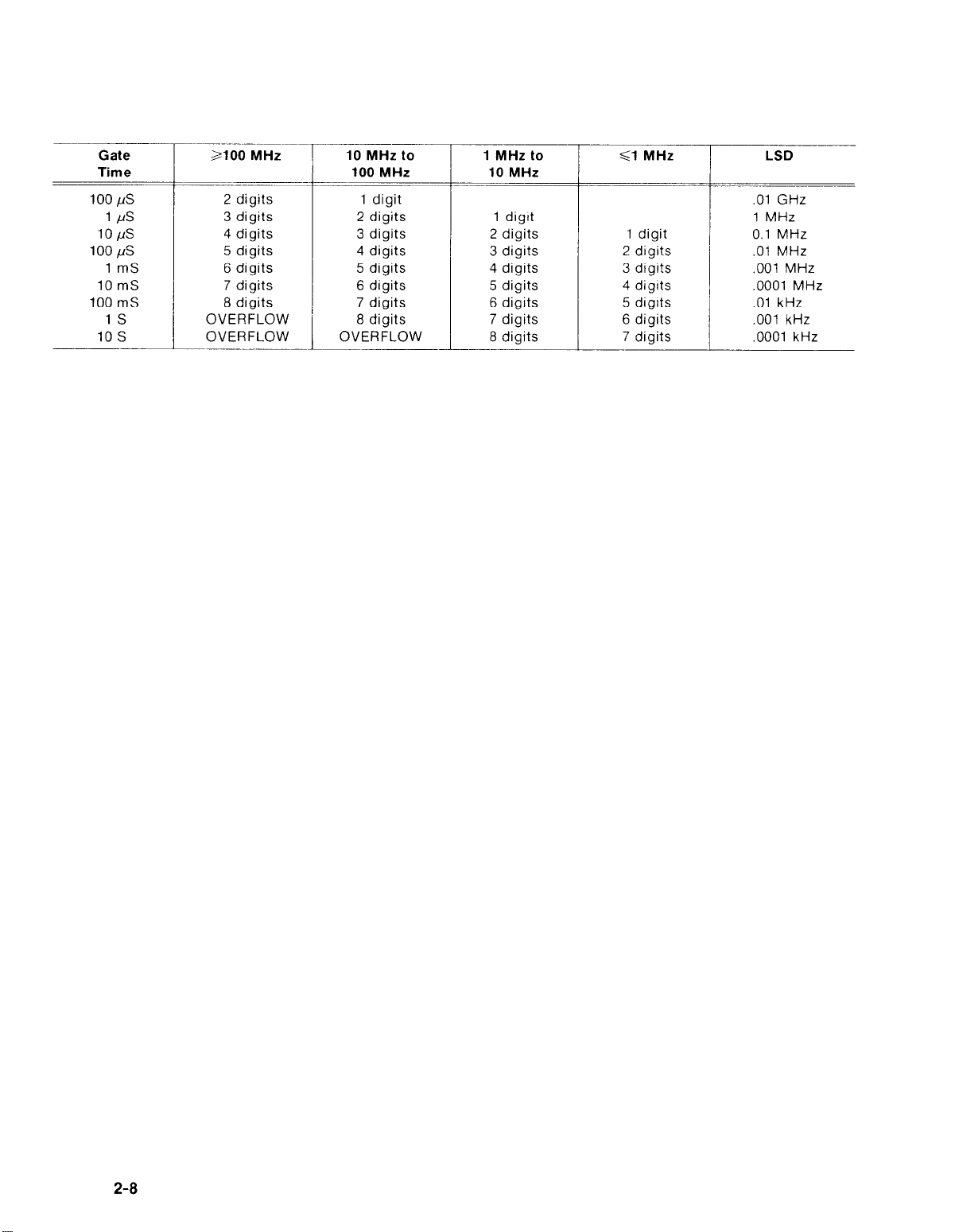
Gate Time vs Measurement Resolution . . . . . . . . . . . . . . . . . . . . . .
PROM Selection Code . . . . . . . . . . . . . . . . . . . . . . . . . . . .
List of Test Equipment Requirements . . . . . . . . . . . . . . . . . . . .
Relative Susceptibility to Static Discharge Damage
2-6
2-6
2-8
3-10
4-2
5-1
iv
Page 7

SECTION 0
GENERAL INFORMATION
TM 9-6625-474-14&P-3
0-1. Scope. This manual contains instructions for
the operator, organizational, direct support, and general support maintenance of and calibration procedures for Tektronix Universal Counter/Timer, Model DC
503A. Throughout this manual, Tektronix Universal
Counter/Timer, Model DC 503A is referred to as the
DC 503A.
0-2. Indexes of publications. a. DA Pam 310-4.
Refer to the latest issue of DA Pam 310-4 to determine whether there are new editions, changes, or
additional publications pertaining to Tektronix Universal Counter/Timer, Model DC 503A.
b. DA Pam 310-7. Refer to the latest issue of DA
Pam 310-7 to determine whether there are modification work orders (MWO’S) pertaining to Tektronix
Universal Counter/Timer, Model DC 503A.
0-3. Forms, Records, and Reports. Department of
Army forms and procedures used for equipment maintenance and calibration are those prescribed by TM
38-750, The Army Maintenance Management System.
Accidents involving injury to personnel or damage to
materiel will be reported on DA Form 285, Accident
Report, in accordance with AR 385-40.
0-4. Reporting Equipment Improvement Recommendations (EIR). If your DC 503A needs im-
provement, let us know. Send us an EIR. You, the
user, are the only one who can tell us what you don’t
like about your equipment. Let us know why you don’t
like the design. Tell us why a procedure is hard to
perform. Put it on an SF 368 (Quality Deficiency
Report). Mail it to Commander, U.S. Army Missile
Command, ATTN: DRSMI-QMD, Redstone Arsenal,
AL 35898-5290. We’ll send you a reply.
0-5. Administrative Storage. To prepare the Tektronix Universal Counter/Timer, Model DC 503A for
placement into and removal from administrative storage, refer to Section 3, Chapter 4, AR 750-25-1,
Maintenance of Equipment and Supplies. Temporary
storage should be accomplished in accordance with
TB 750-25-1, Section 2, Maintenance of Supplies and
Equipment.
0-6. Destruction of Army Electronics
Materiel. Destruction of Tektronix Universal Counter/
Timer, Model DC 503A to prevent enemy use shall be
in accordance with TM 750-244-2.
0-1
Page 8
TM 9-6625-474-14&P-3
0-2
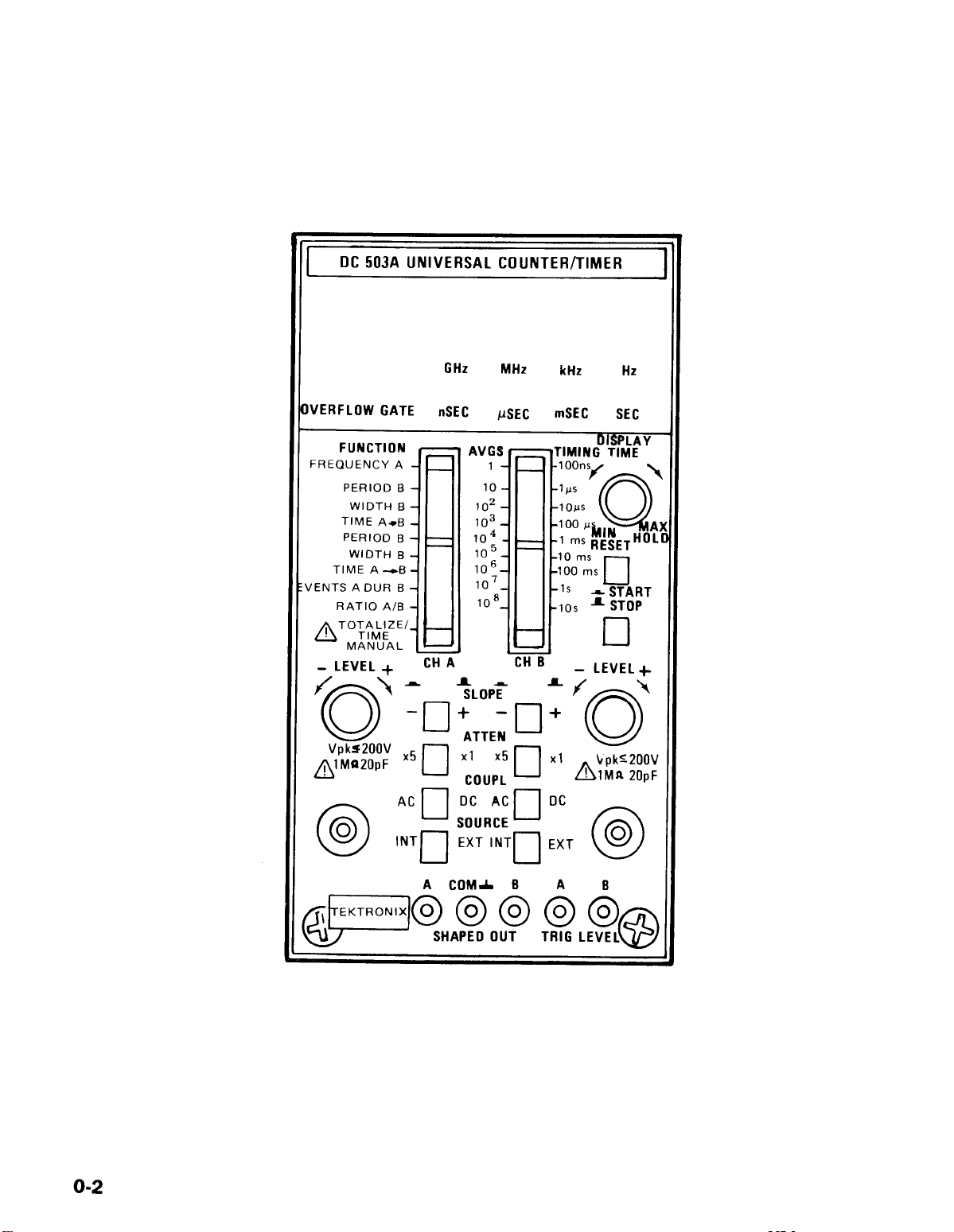
Fig. 0-1. DC 503A Universal Counter/Timer
Page 9

SECTION 1
SPECIFICATION
TM 9-6625-474-14&P-3
Instrument Description
The DC 503A Universal Counter/Timer is designed to
operate in a TM 500-series power module.
The instrument has two input channels, CH A and CH
B, each with 125 MHz capability. Each channel has
separate triggering level, triggering slope, attenuator, and
coupling mode controls.
The DC 503A has eight measurement functions: FREQUENCY A, PERIOD B, WIDTH B, TIME A - B,
RATlO A/B, EVENTS A DURING B, TOTALIZE A, and
TIME MANUAL. All of the modes except FREQUENCY A,
TOTALIZE A, and TIME MANUAL have the capability of
averaging the selected measurement over a range of 1 to
10*
times the input signal. The signals to be counted or
measured can be applied via front panel bnc connectors or
through the rear Interface.
The triggering level for each channel can be monitored
via the front panel or the rear i nterface connections. The
buffered voltage available at these connectors corresponds to the trigger levels set by the front panel
controls.
The output of the internal signal shaping circuits can
also be monitored via front panel connectors. These
shaped signal outputs are useful in setting the triggering
points on complex waveforms.
Instrument Options
Option 01 replaces
(clock) circuit with
temperature controlled oven oscillator for increased accuracy and stability.
Standard Accessories
1 Instruction Manual
1 Cable assembly, bnc-to-tip jack.
Refer to the tabbed Accessories page at the rear of
this manual for more information.
Performance Conditions
The limits stated in the Performance Requirements
columns of the following tables are valid only if the
DC 503A has been calibrated at an ambient temperature
between +20°C and +30°C and is operating at an ambient
temperature between
stated.
the internal 10 MHz time base
a self-contained proportional
NOTE
O“C
and
+50”C,
unless otherwise
Measurement results are displayed in an eight digit
LED readout. The decimal point is automatically positioned and leading zeros are blanked. Single annunciators
(LEDs) are used to indicate register overflow, active gating
interval, and the frequency or time units associated with
the measurement being made.
The DC 503A can be equipped with an optional, oven
controlled, 10 MHz crystal oscillator to obtain a highly
stable and precise internal time base. Both the optional
oscillator and the standard 10 MHz time bases provide
100 ns single shot resolution.
Information given in the Supplemental Information and
Description columns of the following tables is provided for
user information only and should not be interperted as
Performance Check requirements.
The DC 503A must be operated or stored in an
environment whose limits are described under Environmental Characteristics.
Allow at least 20 minutes warm-up time for operation to
specified accuracy, 60 minutes after storage in a high
humidity environment.
1-1
Page 10
TM 9-6625-474-14&P-3
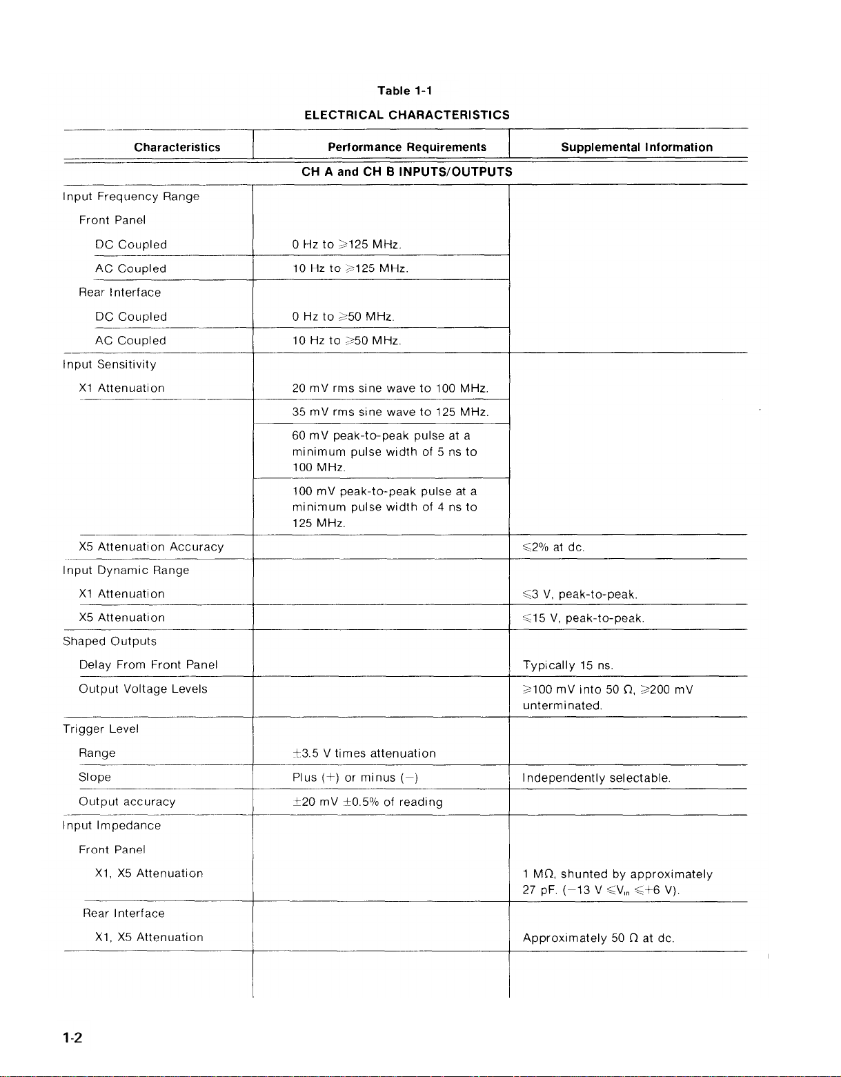
Table 1-1
1-2
Page 11
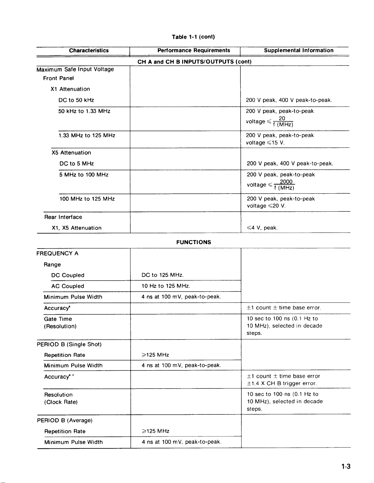
Table 1-1
TM 9-6625-474-14&P-3
1-3
Page 12
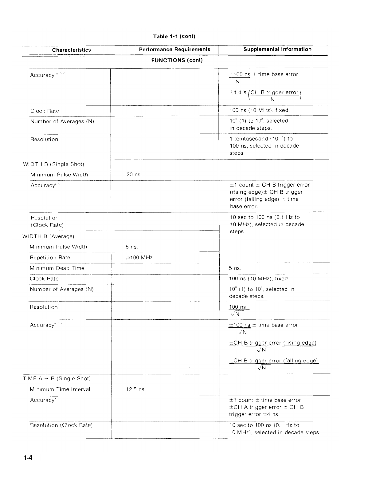
TM 9-6625-474-14&P-3
Table 1-1
1-4
Page 13
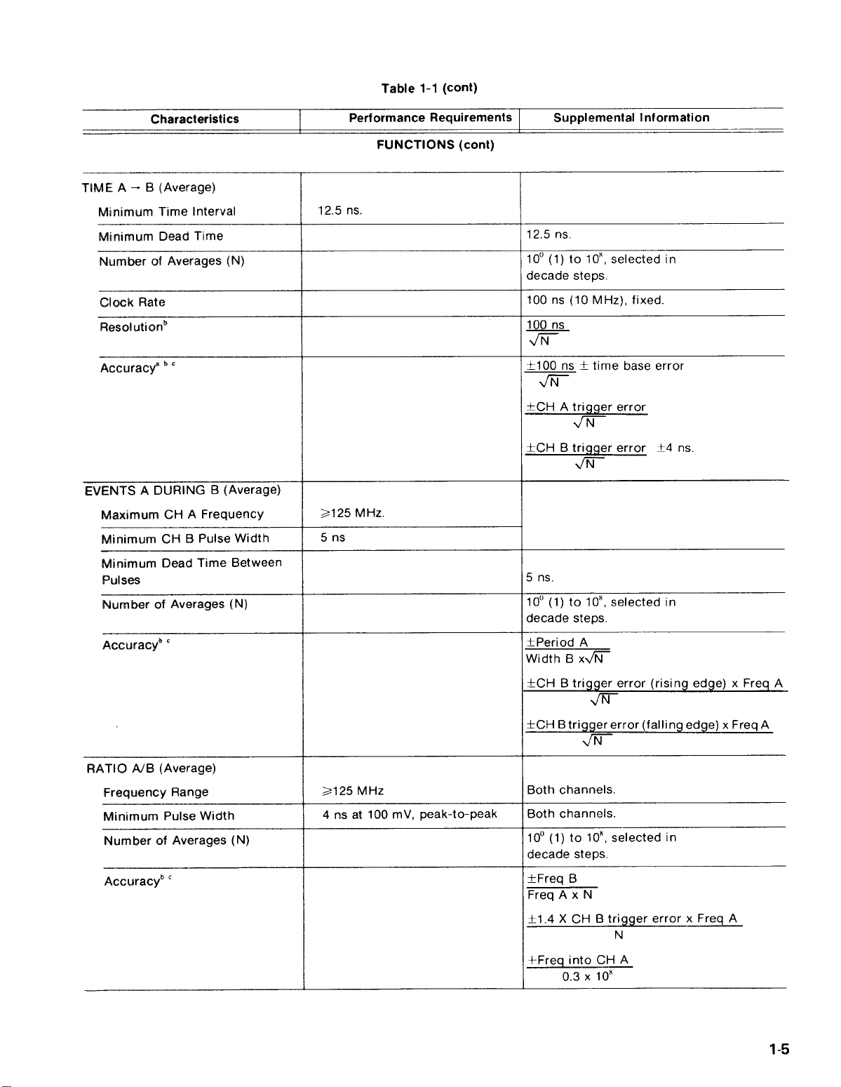
Table 1-1
TM 9-6625-474-14&P-3
1-5
Page 14
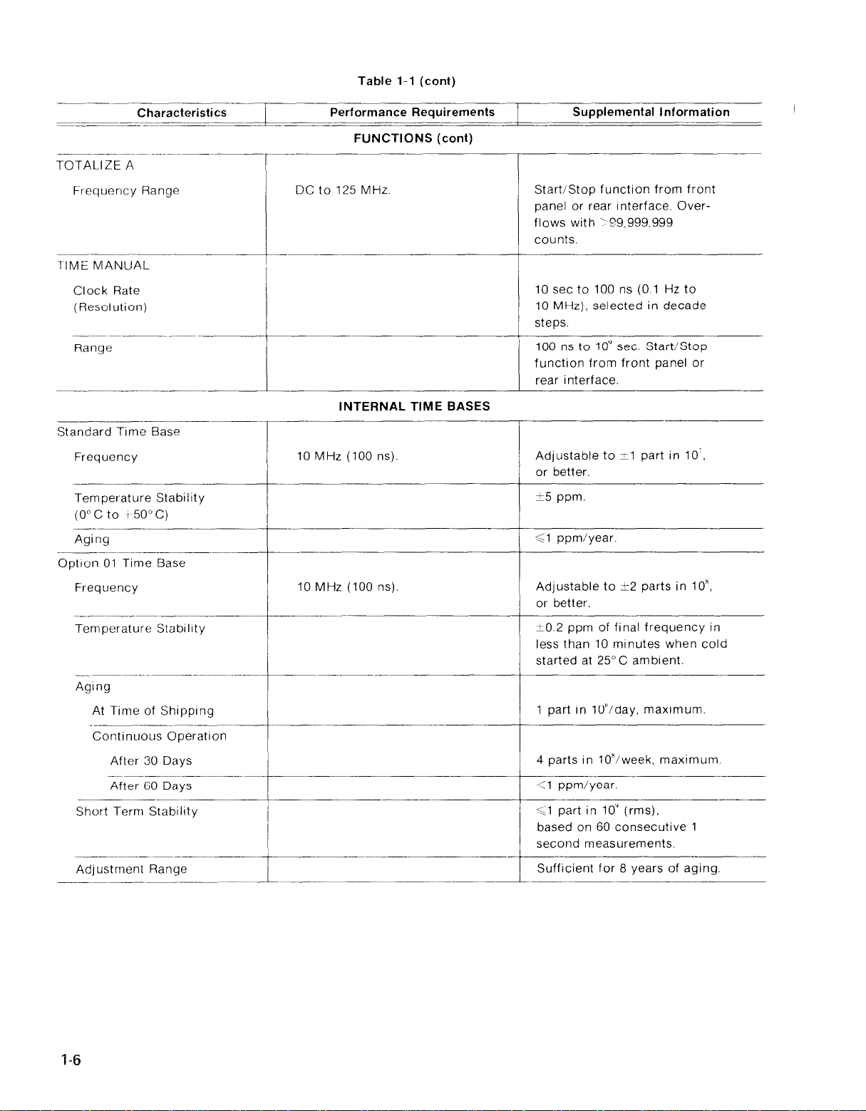
TM 9-6625-474-14&P-3
Table 1-1
1-6
Page 15
Table 1-1
Table 1-2
TM 9-6625-474-14&P-3
Table 1-3
1-7
Page 16
TM 9-6625-474-14&P-3
Table 1-3
Table 1-4
1-8
Page 17
TM 9-6625-474-14&P-3
SECTION 2
OPERATING INSTRUCTIONS
INTRODUCTION
This section of the manual provides installation and
removal instructions and the operating information re-
quired to obtain the most effective performance from the
instrument. Also included is the function of all front panel
controls and a general description of the operating modes,
which also describes procedures for making basic
measurements.
INSTALLATION AND REMOVAL
The DC 503A is calibrated and ready to use when
received. It operates in one compartment of a TM 500-
Series power module. Refer to the power module instruc-
tion manual for line voltage requirements and power
module operation.
To prevent damage to the DC 503A, turn the power
module off before installation or removal of the
instrument from the mainframe. Do not use excessive force to install or remove.
press firmly to seat the circuit board edge connector in the
power module interconnecting jack. Apply power to the
DC 503A by operating the power switch on the power
module.
To remove the DC 503A from the power module, pull
the release latch (located in the lower left corner) until the
interconnecting jack disengages. The DC 503A will now
slide straight out.
Check to see that the plastic barriers on the inter-
connecting jack of the selected power module compart-
ment match the cutouts in the DC 503A circuit board edge
connector. If they do not match, do not insert the
instrument until the reason is investigated. When the units
are properly matched, align the DC 503A chassis with the
upper and lower guides of the selected compartment (see
Fig. 2-1). Insert the DC 503A into the compartment and
Fig. 2-1. Plug-in installation/removal.
2-1
Page 18
TM 9-6625-474-14&P-3
CONTROLS AND CONNECTORS
Even though the DC 503A is fully calibrated and ready
to use, the functions and actions of the controls and
connectors should be reviewed before attempting to use
it.
With the exception of the TOTALIZEA/TIME MANUAL
jumper, which is described in the maintenance section, all
controls for operation of the DC 503A are located on the
front panel. A brief functional description of these controls
follows (refer to Fig. 2-2).
NOTE
Because the Channel A and Channel B controls are
identical, only Channel A will be described.
DISPLAY AND UNIT INDICATORS
DISPLAY READOUT: eight-digit, seven segment
LED readout with automatically positioned decimal
point.
OVERFLOW: when illuminated indicates register
overflow.
MODE SELECTION AND
CONTROL FUNCTIONS
FUNCTION: selects the measurement, events, or
time counting modes for the counter.
NOTE
The TOTALIZE A/TIME MANUAL position is an
"either/or"
MANUAL is selected and set by positioning an
Internal jumper. Placement of this jumper is discussed in the maintenance section.
Unless you are qualified to do so, refer positioning of
this jumper to qualified personnel.
AVGS/TIMING: depending on the position of the
FUNCTION switch, this switch selects the clock rate
which will be counted or the number of
measurements to be averaged.
function.
TOTALIZE A or TIME
GATE: indicates the state of the main gate. When lit,
the main gate is open (the DC 503A is in the process
of making a measurement). When the light is off, the
gate is closed.
GHz/nSEC: when illuminated, indicates the displayed number is gigahertz (GHz) in FREQ A mode
or nanoseconds (nSEC) in a time mode.
MHz/uSEC:
played number is Megahertz (MHz) in FREQ A mode
or microseconds
kHz/mSEC: when illuminated, indicates the displayed number is kilohertz (kHz) in FREQ A mode or
milliseconds (m SEC) in a time mode.
Hz/SEC: when illuminated, indicates the displayed
number is Hertz (Hz) in FREQ A mode or seconds
(SEC) in a time mode.
when illuminated, indicates the dis-
(HSEC)
in a time mode.
2-2
DISPLAY TIME: sets the length of time the reading
will be displayed after the count is made and before
the next measurement is taken, Display time can be
varied from about 0.1 second, fully counterclockwise (ccw), to about 10 seconds fully clockwise
(cw). The HOLD position provides continuous display until reset by pushing the RESET button,
RESET: momentary switch resets the count to zero
when operating in the TOTALIZE A mode. Also acts
as a master reset, ensuring that the readout has been
cleared before the next measurement. Provides a
check of all display LED’s; when pressed, a row of 8’s
will be displayed in the readout window.
START/STOP: push-push switch acts as a manual
gate when the FUNCTION switch is in the
TOTALIZE A/TIME MANUAL position. Button in
Starts the measurement interval gate; button out
terminates the gate.
Page 19
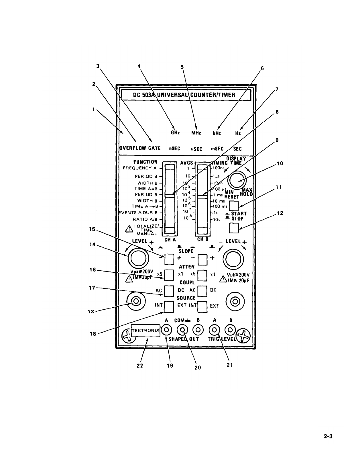
TM 9-6625-474-14&P-3
Fig. 2-2. Controls and connectors.
2-3
Page 20
TM 9-6625-474-14&P-3
CHANNEL A INPUT AND LEVEL
FUNCTIONS
CH A INPUT: bnc connector for Channel A signal
input. Input impedance is 1 shunted by approximately 20 pF.
LEVEL: selects the amplitude point on the positive or
negative slope of the input signal at which the
triggering window is placed.
SLOPE: push-push switch selects the slope of the
input signal on which triggering will occur, Button
out selects plus (+) slope; button in minus (–) slope.
ATTEN: push-push switch selects X1 (button out) or
X5 (button in) attenuation of the input signal.
COUPL: push-push switch selects DC (button out)
or AC (button in) coupling of the input signal to the
attenuator circuit.
SOURCE: push-push switch selects the source of
the input signal. Button out, EXT, selects the front
panel connector as a signal source. Button in, INT,
routes the input signal to the counter via the rear
interface connections.
SHAPED OUT A: provides a shaped output signal
derived from the output of the Channel A signal
shaper circuitry.
SHAPED OUT GND: common connector for
Channel A shaped output signals.
TRIG LEVEL A: pin jack permits monitoring of the
Channel A triggering voltage level.
RELEASE LATCH: pull to disengage and remove
DC 503A from the power module.
INPUT CONSIDERATIONS
Input Sources
NOTE
Maximum input voltage limited to 200 V peak.
The SOURCE switch for each channel selects either the
front panel bnc connector (external), or the rear interface
connector (internal) pins. The external inputs present
impedances of approximately 1 paralleled by about 27
pF. The internal input circuits present nominal 50
impedances to match typical coaxial cable signal connections.
Input Coupling
Front panel pushbuttons select ac (capacitive) or dc
(direct) coupling for the input signal of each channel. This
coupling takes place before the signals are passed into the
attenuator circuits.
Attenuators and Maximum Input Volts
For either attenuation factor, X1 or X5, the maximum
safe input voltatage that can be applied to the front panel
bnc connectors is 200 V (peak) from dc to 50 kHz. At
frequencies above 50 kHz, the maximum safe peak-to-
peak input voltage tothe front panel bnc connectors must
be calculated (see Specification section). The maximum
safe input voltage to the rear interface input connectors is
equal to or less than 4 V (dc plus peak ac) from dc to
50 MHz.
Sensitivity and Frequency Range
CH A and CH B will respond to a signal amplitude of
20 mV rms sinewave, times attenuation, to lOO MHzandto
a sinewave of 35 mV rms, times attenuation, to 125 MHz.
[)
Depending on the coupling mode selected, the low
frequency limit for each channel is either zero (dc
coupled) or 10 Hz (ac coupled).
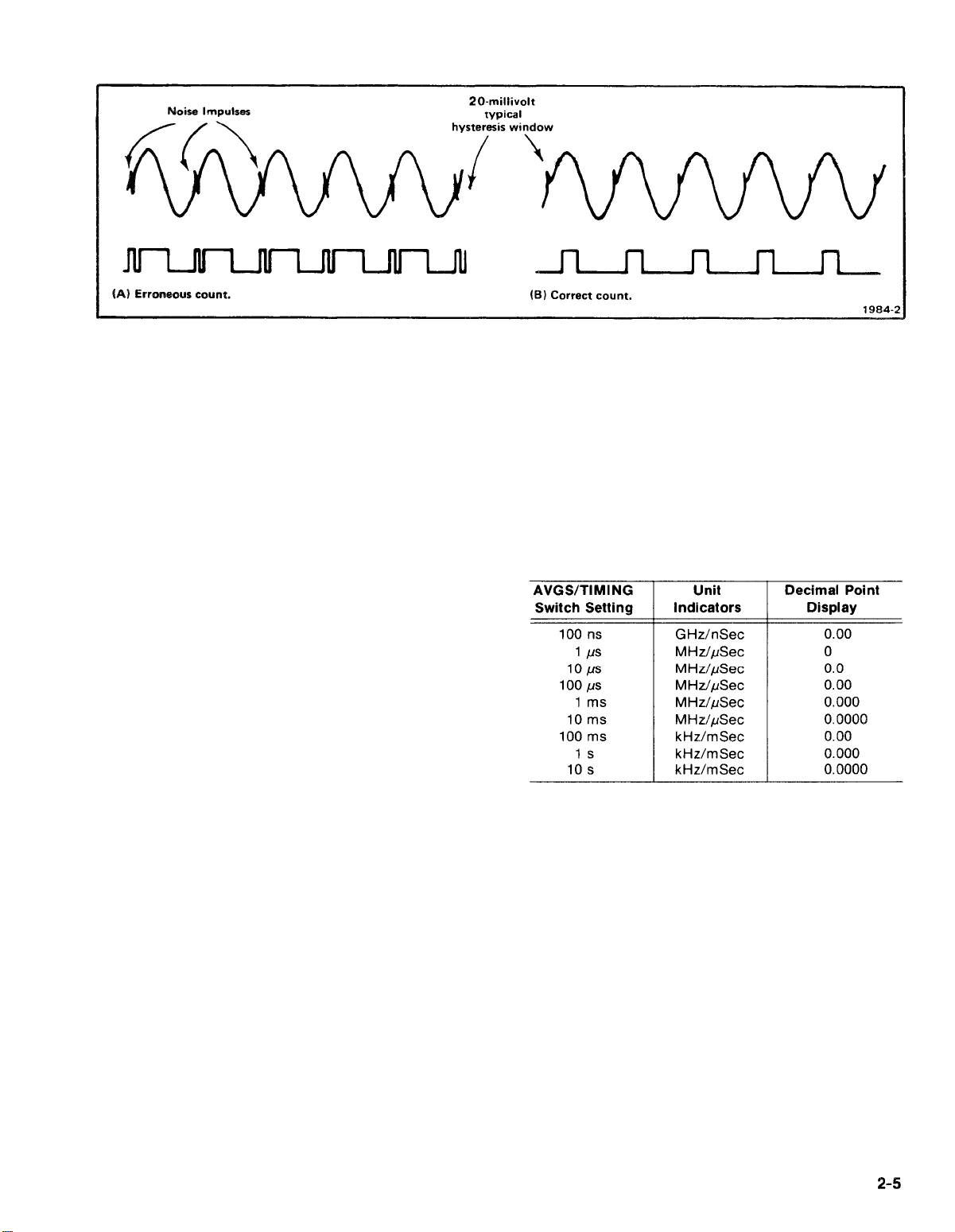
Slope and Level
The SLOPE pushbuttons for each channel determine
whether the trigger circuits will respond to the negative or
positive transition of the input signal.
Refer to Fig. 2-3. The LEVEL control for each channel
allows the operator to move the hysteresis window of the
trigger circuit to an optimum level on the input signal to
ensure stable triggering The LEVEL control adjusts over
+3.5 V, times attenuation, of the input signal. This level
can bemoniiored atthefront panel TRIG LEVEL pin jacks.
2-4
Page 21
TM 9-6625-474-14&P-3
Fig. 2-3. Triggering circuit response to improper (A) and proper (B) level settings.
OPERATORS FAMILIARIZATION
PREPARATION
Turn on the power module to apply power to the
DC 503A. One or more characters in the display should be
visible. Allow twenty minutes warm-up time for operation
to specified accuracy.
DISPLAY TESTS
With no signal applied, test the DC 503A readout
displays and switching logic. The following checks will
test most of the major circuits of the counter and ensure its
readiness to make measurements. If any malfunctions are
encountered, refer
personnel.
Readout Segment
Press the RESET
segments of each digit. A row of 8's should be displayed.
This check of the display devices can be done at anytime.
the condition to qualified service
Test
button to check the seven character
Table 2-1
FREQUENCY A DISPLAY CHECK
With the DISPLAY TIME control in the fully
counterclockwise position, observe that the GATE indicator flashes rapidly for short gate times and more
slowly for longer gate times. Using a short gate time
(100 ms), rotate the DISPLAY TIME control slowly
clockwise. Observe that the GATE indicator stays off for a
longer and longer time, until the control clicks into the
HOLD (detent) position, holding off the gate indefinitely.
Return
counterclockwise position.
the DISPLAY TIME control to the
Frequency A Displays
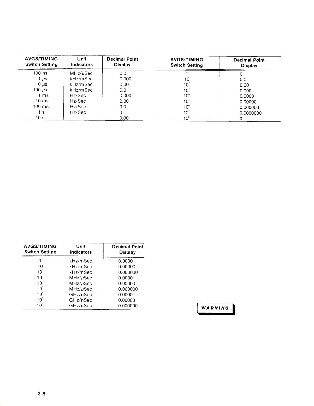
Set the FUNCTION switch to FREQUENCY A. With the
AVGS/TIMING switch, select a gate time of 100 ns. Check
the decimal point location, leading zero suppression, and
units indicators according to Table 2-1.
Period B, Width B, and Time A - B Displays
Timing Mode. Set the FUNCTION switch to PERIOD B
in the blue area of the front panel and the AVG/TIMING
switch to 100 ns. Observe the correct readout displays as
shown in Table 2-2.
2-5
Page 22
TM 9-6625-474-14&P-3
Table 2-2
PERIOD B, TIME A - B, WIDTH B
(TIMING MODE) DISPLAY CHECK
Set the FUNCTION switch to WIDTH B in the blue area
of the front panel while retaining the setting of the
AVG/TIMING switch; observe the correct readout display.
Set the FUNCTION switch to TIME A - B in the blue
area of the front panel while retaining the setting of the
AVG/TIMING switch; observe the correct readout display.
Table 2-4
RATIO A/B AND EVENTS A
DURING B DISPLAY CHECK
Time Manual Displays
Verify that the jumper located on the Auxiliary Circuit
Board is in the TIME MANUAL position. Set the FUNCTION switch to the TIME MANUAL Position and the
AVGS/TIMING switch to 1 sec.
Averaging Mode. Repeat the preceding checks for
these functions in the dark grey area of the front panel.
Observe the correct readout display for each switch
setting as shown in Table 2-3.
Table 2-3
PERIOD B, TIME A - B, WIDTH B
(AVERAGING MODE) DISPLAY CHECK
Events A During B and Ratio A/B Displays
Set the FUNCTION switch to EVENTS A DURING B
and the AVGS/TIMING switch to 1. Check the readout
displays according to Table 2-4.
Set the FUNCTION switch to RATlO A/B and the
AVGS/TIMING switch to 1. Again check the readout
displays using Table 2-4.
The GATE indicator should light and an advancing
count should be displayed when the START/STOP button
is pushed in. The GATE indicator should go out when the
count is stopped by releasing the START/STOP button.
Check the overflow display by setting the AVGS/TIMING
switch to 100 ns pressing the START/STOP button in, and
letting the count advance, When the last decade (eighth
digit) goes from nine to zero the OVERFLOW indicator will
light. Release the START/STOP button and observe that
the OVERFLOW indicator remains on, but the count does
not change. Pressing the RESET button clears the
overflow condition, sets the count to zero, and extinguishes the OVERFLOW indicator.
Totalize A Display
For this check, the jumper located on the Auxiliary
Circuit Board must be in the Totalize position.
Unless you are qualified to do so, refer placement of
this jumper to qualified personnel.
Set the FUNCTION switch to the TOTALIZE A/TIME
MANUAL position. Observe a zero at the right of the
readout display. The GATE indicator should light when
the START/STOP button is pushed in, and go out when
the button is released. The units indicators and decimal
points should remain off.
2-6
Page 23

TM 9-6625-474-14&P-3
Channel A Slope
Verify that the TOTALIZE/TIME MANUAL jumper is in
the TOTALIZE position. With the FUNCTION switch set to
TOTALIZE A/TIME MANUAL and CH A to + SLOPE
(button out), press the START/STOP button. Turn the CH
A LEVEL control fully clockwise. The readout display
should increase one count each time the control is rotated
from clockwise to counterclockwise (past center position). Verify that the count does not increase when the
control is turned from counterclockwise to clockwise.
Change to - SLOPE (button in) and push the RESET
button to clear the display. The readout should now
increase one count each time the CH A LEVEL control is
rotated from counterclockwise to clockwise (past center).
Turning the control from clockwise to counterclockwise
should not increment the display.
OPERATING MODES
GENERAL
The following discussion provides general information
about each mode of operation and instructions on making
measurements for FREQUENCY A, RATIO A/B, TIME
INTERVAL (WIDTH B and TIME A - B), EVENTS A
DURING B, and TOTALIZE.
FREQUENCY A MODE
In this mode the input signal isconnectedto CH A Input
only, either through the rear interface or the front paneI
connector. Use ac coupling for most frequency
measurements to avoid readjusting the LEVEL control
because of changing dc levels. The repetitive nature of the
signals makes slope selection unnecessary for frequency
measurements. Signals less than 3 volts peak-to-peak
need not be attenuated; larger signals should be
attenuated to within the range of 60 mV to 3 V peak-topeak.
Channel B Slope
Set the FUNCTION switch to PERIOD B, CH B to +
SLOPE (button out), and the AVGS/TIMING switch to 1.
Push the RESET button. Check that the GATE indicator
turns on when the CH B LEVEL control is rotated from
clockwise to the counterclockwise position. Turning the
control back to clockwise should have no effect on the
GATE indicator. Another turn from clockwise to
counterclockwise turns the GATE indicator off.
Change to - SLOPE (button in) and press the RESET
button. Observe that rotating the CH B LEVEL control
from counterclockwise to clockwise and back produces
an action that is just opposite that described in the
preceding paragraph.
changes unreasonably, the DC 503A is not being
triggered properly, either because the controls are not
correctly set or the signal is beyond the capabilities of the
counter.
Measurement Intervals. To adjust the trigger controls,
choose a short gate time such as .1 second or .01 seconds.
This gives rapid feedback via the display whether or not
the counter is being triggered. Final selection of gate time
depends upon the frequency being measured, desired
resolution, and willingness of the operator to wait for a
measurement.
Resolution. A 10 second gate time means the operator
must wait 10 seconds for a measurement to be made and
displayed. This will give 0.1 Hz resolution. A 10 second
count will display fewer than the available eight digits for
any signal below 10 MHz.
Set the FUNCTION switch to FREQUENCY A and, with
the AVGS/TIMING switch, select one of the shorter gate
times. Set the DISPLAY TIME control fully counterclockwise. Connect the signal to be measured to the
input and adjust the LEVEL control for a stable display.
The LEVEL control setting should not be critical unless the
signal amplitude and frequency are close to the specified
limits.
If the count varies from reading to reading, it is
probably caused by jitter in the signal source. If the count
Overflow. Through intentional use of “overflow” dis-
plays, it is possible to improve the resolution of the
counter. Select a gate time that displays the most significant digit as far to the left as possible. Note the numbers
displayed to the right of the decimal. Move the decimal to
the left, by selecting longer gate times, until the desired
resolution is achieved. The OVERFLOW indicator will light
when the most significant number overflows the last
storage register. The relationship between gate time,
measured frequency, displayed digits, and overflow is
shown in Table 2-5.
2-7
Page 24
TM 9-6625-474-14&P-3
GATE TIME
Table 2-5
VS MEASUREMENT RESOLUTION
Measurement Rate. Once a stable measurement is
obtained, the rate at which measurements are made can
be controlled by the DISPLAY TIME control. Turning the
control clockwise holds off the gate and stores the display
for a longer time before a new measurement is made and
displayed. Display time and gate time together complete a
measurement-display cycle.
The DISPLAY TIME control is uncalibrated and
variable from about 0.1 second (in the MIN position) to
about 5 seconds. At the extreme clockwise end of the
control is a detent position called HOLD. In HOLD, the last
count taken will be stored and displayed for an indefinite
period. A new count and display can be initiated by
pressing the RESET button, moving the DISPLAY TIME
control out of the detent, or changing the gate time.
PERIOD MODES
The period and period average modes allow single
period measurements or multiple period averages to be
made with input frequencies into CH B. These modes are
useful for making low frequency measurements where
maximum resolution is desired without waiting for long
measurement time. Simply stated, the PERIOD B mode
reverses the functions of signal and clock as compared to
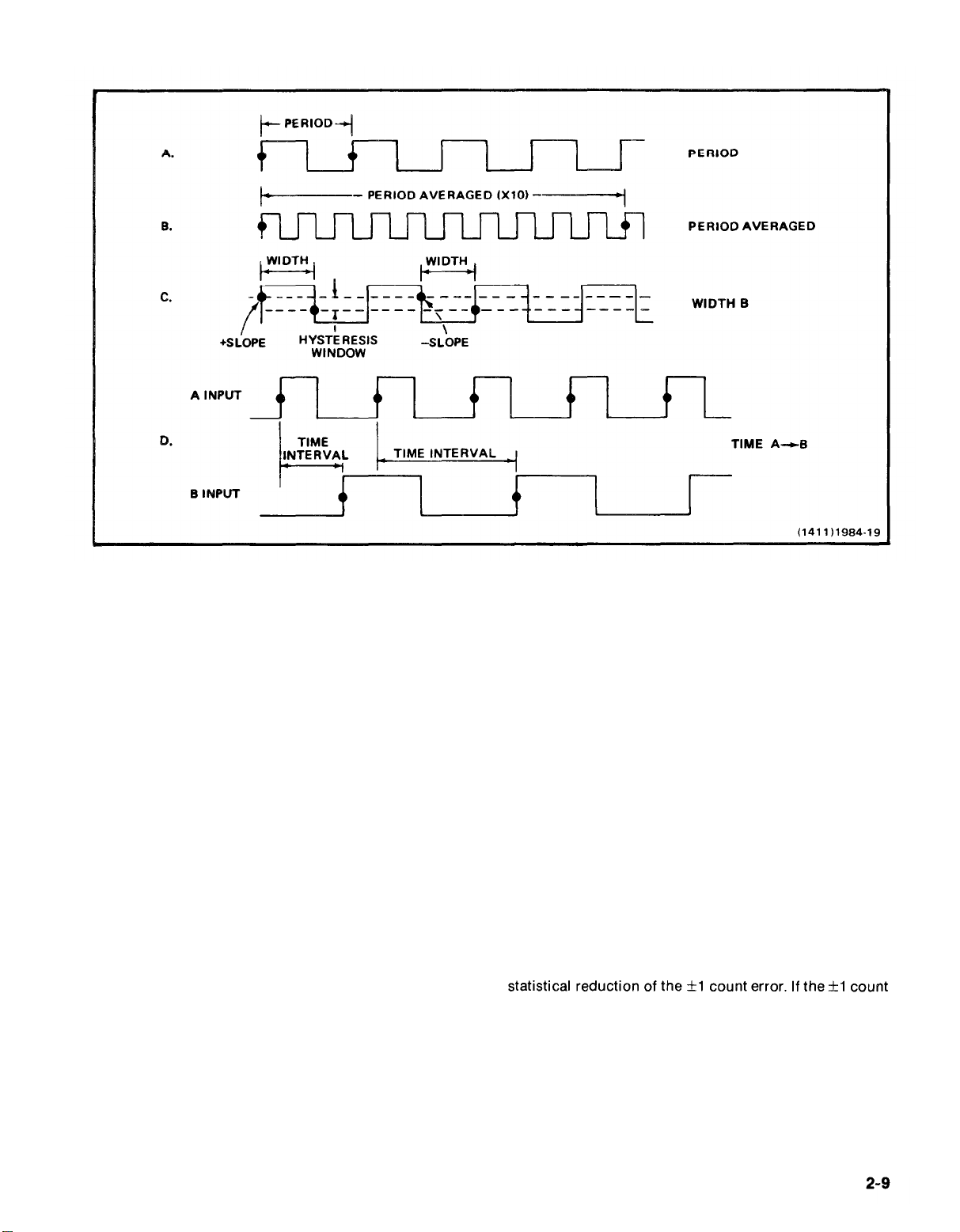
FREQUENCY A mode. Refer to Fig. 2-4A.
Averaging. Resolution and accuracy is improved by
averaging the signal value over a large number of signal
events. This increases the total time to take a measurement, i.e., similar to selecting a longer gate time in
FREQUENCY A mode. Refer to Fig. 2-4B.
preferred. Other wave shapes can be accurately measured
if the amplitude is kept high.
TIME INTERVAL MODES
Two modes of time interval measurement can be
selected: WIDTH B, and TIME A - B. The WIDTH B mode
measures the time between two points on a waveform,
These two points are selected by the CH B triggering
controls such that the counter main gate turns on at the
point selected by the CH B SLOPE and LEVEL controls,
and turns off at the same level but the opposite slope,
Refer to Fig. 2-4C.
The TIME A - B mode measures the time between two
points on two waveforms. These two points are controlled
such that the CH A triggering controls select the point at
which the main gate turns on, andthe CH B controls select
the point at which the main gate turns off. Refer to Fig. 2-
4D.
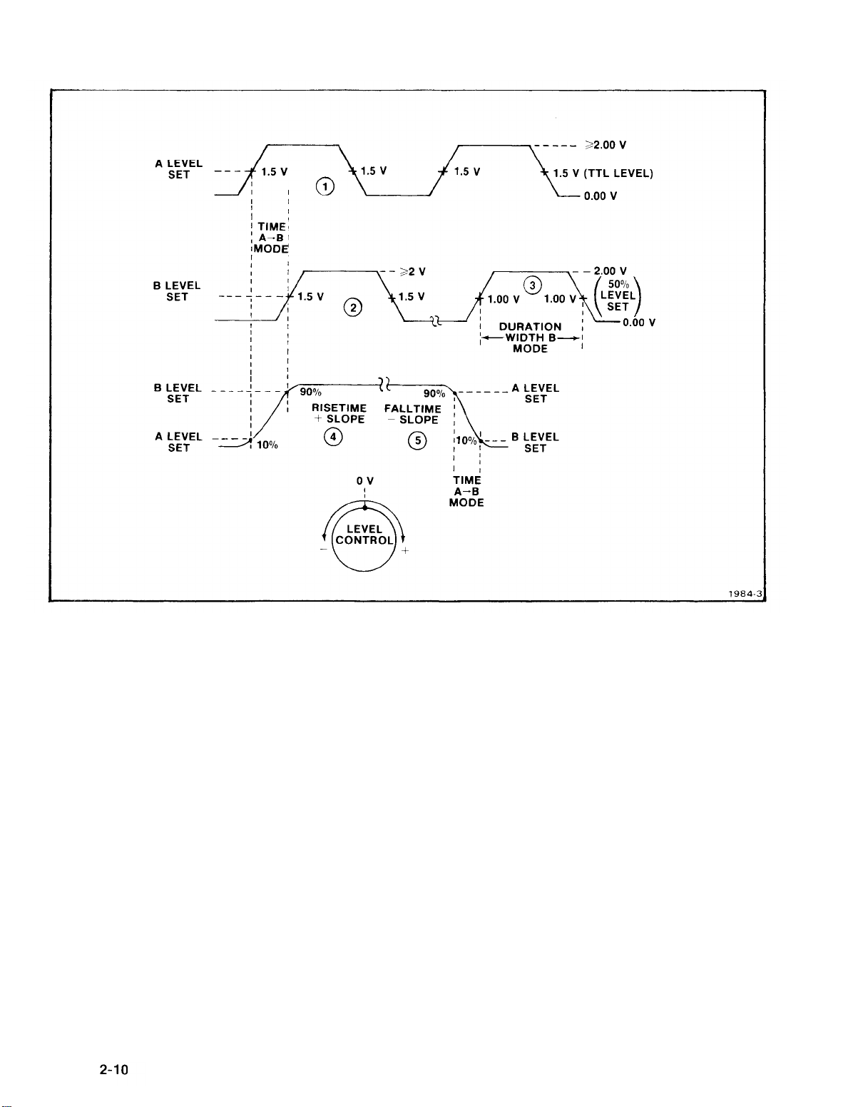
Triggering. The voltage levels necessary to establish
the triggering points on any selected slope are monitored
and set with digital voltmeter readings at the CH A/CH B
TRIG LEVEL pin jacks on the front panel or rear interface
connections. Fig. 2-5 illustrates typical TRIG LEVEL
voltage settings for various time interval measurements.
When making these measurements, each channel must be
dc coupled and coaxial cables must be properly terminated in order to maintain signal fidelity.
Low Frequencies. Period Measurements of signals
below 10 Hz, and particularly in the lowest decade from
0.1 Hz to 1.0 Hz, become rather sensitive to wave shape
and amplitude. Since it is desirable for the signals to pass
through the trigger hysteresis abruptly, square waves are
2-8
WIDTH B Mode. In order to measure pulse duration
(Fig. 2-5, waveform 3), the 50% level must be determined.
Set the FUNCTION switch to WIDTH B and the CH B
LEVEL control fully counterclockwise. Apply the input
signal to the CH B input connector. The GATE indicator
must be off.
Page 25
TM 9-6625-474-14&P-3
Fig. 2-4. Representation of Interval measurements.
Rotate the LEVEL control until the GATE indicator just
come on and record the digital voltmeter reading.
Continue rotating the LEVEL control until the GATE
indicator just goes off and record the digital voltmeter
reading. Subtract the first digital voltmeter reading from
the second and divide by 2; this is the 50% level.
Reset the CH B LEVEL control so that the digital
voltmeter indicates the 50% level. Read the pulse duration
from the DC 503A display.
Time A -
B Mode. This measurement requires input
signals to both CH A and CH B, but the peak-to-peak
signal amplitude should first be determined using the
WIDTH B mode instructions. For TIME A - B
measurements, follow these steps:
1.
Set the FUNCTION switch to WIDTH B.
Referring to WIDTH B mode instructions, determine
2.
the peak-to-peak amplitude and desired triggering
level of the signal to be applied to the Channel B
input.
If the signal to be applied to Channel A input is
3.
different than that being applied to Channel B,
repeat Step 2 for this signal.
4.
Set the Channel B LEVEL control to the desired
triggering level as calculated in Step 2.
5.
Set the FUNCTION switch to TIME A - B.
Set the Channel A LEVEL control to the desired
6.
triggering level as calculated in Step 3.
7.
With signals connected to the proper channels, read
the elapsed time interval between the triggering
level of Channel A and the subsequent triggering
level of Channel B from the DC 503A display.
Time Interval Averaging. Averaging can be used to
increase the accuracy and resolution of repetitive signal
measurements. The basic reason for averaging is the
error is truly random, then as more intervals are averaged,
the measurement will tend to approach the true value of
the time interval. For time interval averaging to work, the
time interval being measured must be repetitive and have a
repetition frequency that is nonsynchronous to the
counter clock rate. The DC 503A will measure up to 10”
averages in both Width B averaging and TIME A - B
averaging.
2-9
Page 26
TM 9-6625-474-14&P-3
Fig. 2-5. Typical CH A and CH B Level Out voltage settings for various time interval measurements.
EVENTS A DURING B MODE
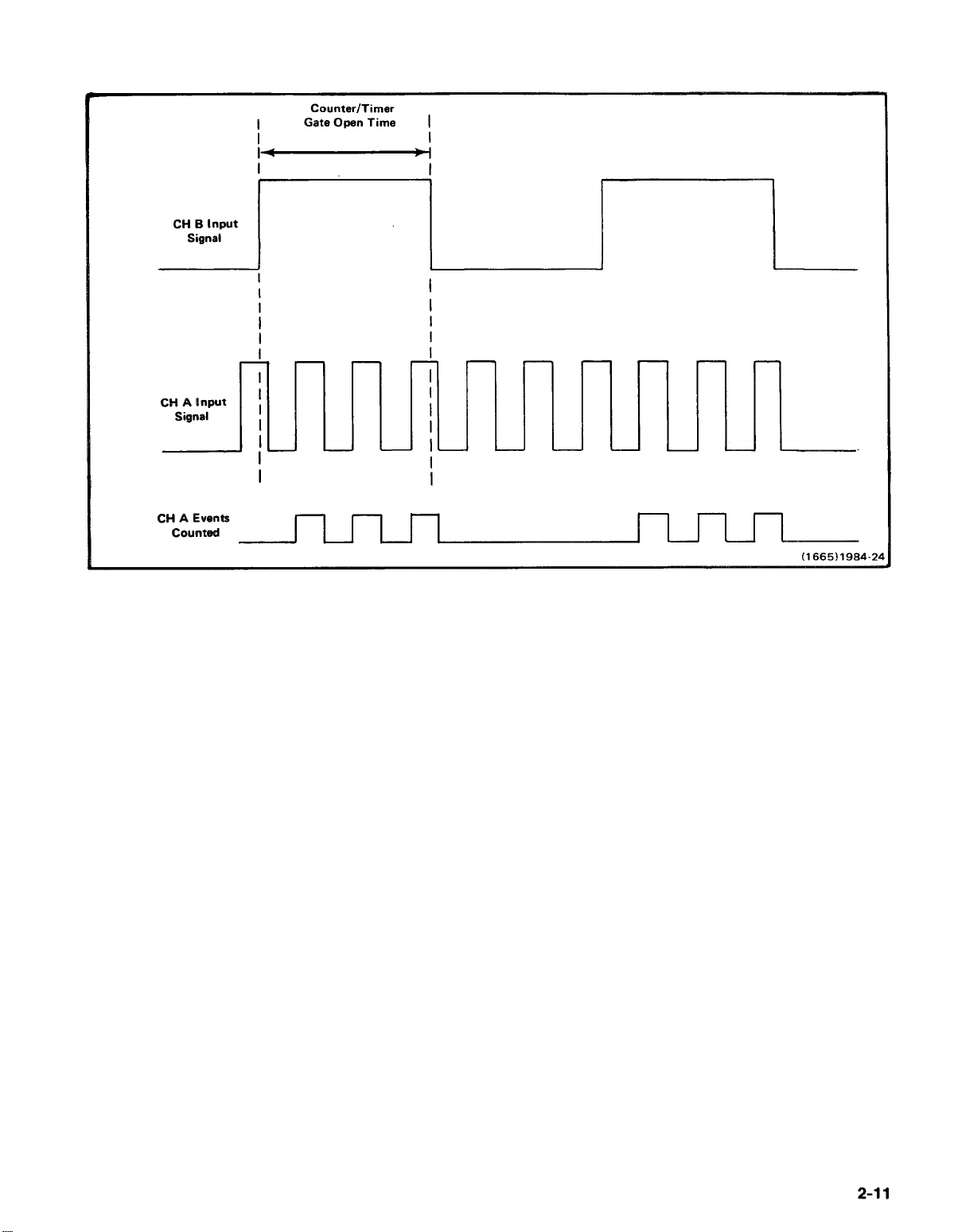
In the EVENTS A DURING B mode, the events applied
to Channel A are counted. The count is gated by the signal
applied to Channel B input. The accumulated total of
events A that arrived during the time signal B was
triggered is displayed in the readout. Refer to Fig. 2-6.
The following procedure can be used to make a
measurement like that shown in Fig. 2-6.
1. Apply the signal to be counted to Channel A. With
the FUNCTION switch at FREQUENCY A, set
Channel A SLOPE switch to + SLOPE. Adjust the
LEVEL control for a stable display.
2. Apply the control signal to Channel B. With the
FUNCTION switch at PERIOD B, set Channel B
SLOPE switch to + SLOPE, Adjust the LEVEL
control for a stable display.
3. Set the FUNCTION switch to EVENTS A DURING B.
When the Channel B signal excursion occurs, Channel
B is triggered andthe gate opens, allowing the Channel A
pulses to be counted.
Averaging. Averaging can be used to Increase the
accuracy and resolution of repetitive event per interval
measurements. As more events are averaged, the
measurement tends to approach the true value of the
number of events per interval.
RATlO MODE
The DC 503A may be used to measure the ratio of two
signals, where one signal is applied to Channel A input
and the other signal is applied to Channel B input.
2-10
Page 27
TM 9-6625-474-14&P-3
Fig. 2-6. Illustration of CH A events counted from portion of CH A signal pulses during the counter gate open time (controlled by
CH B signal).
In the Ratio A/B mode, the frequency of the signal
applied to Channel A is divided by the frequency of the
signal applied to Channel B, and the resultant ratio is
displayed.
measurements, the smallest number of averages that
produces a useful number of digits should be considered.
TIME MANUAL MODE
This mode is a manual analog of the TIME A - B mode.
Triggering. The operation of Channel A and Channel B
trigger controls is the same as for frequency and period
measurements. Set the trigger controls as follows:
1.
Go to the FREQUENCY A mode and adjust the
Channel A trigger controls for a normal frequency
measurement.
Go to the PERIOD B mode and adjust the Channel B
2.
trigger controls for a normal period measurement.
Leaving the Channel A and Channel B trigger
3.
controls as they are, gotothe RATIO A/B mode. The
correct ratio should be displayed.
Resolution. The AVGS/TIMING switch, which controls
the number of averages of the Channel B signal, may now
be set to display maximum resolution. For most
In this mode, only the AVGS/TIMING switch and
START/STOP switch affect the display.
Starting and Stopping. The TIME MANUAL mode may
bethought of as a “stop-watch” type of operation. With the
FUNCTION switch inthe TIME MANUALposition (and the
internal jumper properly positioned), the display starts
counting time-base pulses when the START/STOP switch
is depressed. It will continue to count and display the
accumulated total until the START/STOP switch is released. The last count will then be held in the display until
another START command is given (in which case the
count will again advance), or other controls are actuated.
Pressing the RESET button will return the display to zero.
Changing the setting of the AVGS/TIMING switch will
change the frequency of the time-base pulses being
counted and reset the display to zero. The start/stop
function can also be performed remotely via the rear
interface connections.
2-11
Page 28

TM 9-6625-474-14&P-3
Clocking Rate. When the AVGS/TIMING switch is in
the 1 s position, one-second pulses are being counted and
the display accumulation advances one count per second,
and so on.
Whenever the accumulated count is above 99,999,999,
the OVERFLOW indicator will light to indicate register
overflow; however, the accumulation continues at the
not displayed.
TOTALIZE A MODE
This mode is a manual analog of the FREQUENCY A
mode. lnthismode, signal event sapplied tothe Channel A
input are counted and the accumulated total displayed
during the time the START/STOP button is depressed to
the START position. The main application of this mode is
to accumulate the count of relatively infrequent and
irregular events.
Operation. Apply the signal to Channel A input and set
the trigger controls the same as for a frequency measurement. Only the Channel A trigger controls, the RESET
button, and the START/STOP button affect the display in
this mode.
Starting the Count. Press the START/STOP button and
adjust the Channel A LEVEL control until a count begins to
advance. The accumulated count is displayed in whole
numbers.
will continue to be displayed. No more incoming events
will be added to the total.
Restarting and Resetting. When the START/STOP
button is again depressed, incoming events will advance
the displayed total. Resetting the count to zero can be
done at any time by pressing the RESET button.
Remote start/stop. Starting and stopping the count can
be accomplished remotely via connections to the rear
interface.
REPACKAGING FOR SHIPMENT
If the Tektronix instrument is to be shipped to a
Tektronix Service Center for service or repair, attach a tag
showing: owner (with address) and the name of an
individual at your firm that can be contacted. Include
complete instrument serial number and a description of
the service required.
If the original package is not fit for use or not available,
repackage the instrument as follows:
Surround the instrument with polyethylene sheeting, or
other suitable material, to protect the exterior finish.
Obtain a carton of corrugated cardboard of adequate
strength and having inside dimensions no Iess than six
inches more than the instrument dimensions. Cushion
the instrument by tightly packing dunnageor urethane
foam between the carton and the instrument,
sides, Seal the carton with shipping tape or
dustrial stapler.
on all
an in-
Stopping the Count. If the START/STOP button is
released and no other controls are actuated, the last total
2-12
The carton test strength for your instrument
pounds.
is 200
Page 29
SECTION 3
TM 9-6625-474-14&P-3
THEORY
OF OPERATION
BLOCK DIAGRAM DESCRIPTION
Introduction
For the following block diagram description refer to the
Block Diagram foldout page at the rear of this manual.
Channel A and Channel B Amplifiers
There are two inputs, CH A and CH B. Signals to be
counted or timed are applied to either or both channels via
front panel bnc connectors or via the rear interface. The
front panel inputs for both channels are terminated with an
paralleled with approximately 27 pF. The rear interface
inputs to both channels are terminated with a resistance of
Signal Flouting circuits.
Each channel contains an ac/dc coupling switch, a X1
or X5 attenuation network, a buffer amplifier circuit acting
as a comparator that compares the incoming signal level
against the triggering level as a reference, and
amplifier/Schmitt circuits driving the signal slope selec-
tion functions in the Signal Routing circuits. Each channel
also contains an operational amplifier serving as a X1
buffer circuit, supplying a buffered version of the trigger
level at the front panel tip jacks or rear interface connec-
tions.
NOTE
panel with the proper decimal point location and correct
annunciator illuminated.
The Measurement Cycle Timing circuit determines the
Display Time, clears the Gate Generator circuits, loads
(latches) the decade counters, and resets the counters for
the next measurement cycle in all modes of operation.
PERIOD B (Variable Clock)
In this TIMING mode, the CH B signal is passed
through the Signal Routing circuits to the Gate Generator
Input of the Decade Accumulators and the Measurement
Gate is generated by a single period of the signal from
Channel B. As before, the accumulated count for this
mode and all subsequent modes is latched, decoded from
BCD data to 7-segment information, and displayed on the
front panel with the correct annunciator illuminated and
the proper decimal point location.
PERIOD B (Averageable—100 ns Clock)
For this AVGS mode, the Time Base signal
(10 MHz = 100 ns) is not divided; it is applied through the
Signal Routing circuits directly to the Count Input of the
Decade Accumulators. The CH B signal is routed to the
The remainder of this block diagram description
discusses the signal paths through the remaining
circuit blocks and the typical events related to each
mode of operation (FUNCTION) listed on the front
panel.
FREQUENCY A (Variable Gate)
For this mode of operation the CH A signal passes
directly through the Signal Routing circuits to the Decade
Accumulators. The signal is counted by the 1st DCU, then
the 2nd DCU, and then by the 6-Decade Counter (a total of
eight decades). In the FREQUENCY A mode the Time
generate a Measurement Gate (via the Gate Generator) for
the desired measurement time. At the end of the Measure-
ment Gate interval, the accumulated count is latched in
the 8-Decade Latch/Multiplexer circuits, converted from
BCD to 7-segment information and displayed on the front
of the CH B signal. The Time Base is counted for 10”
periods before the accumulated count is latched for
display.
WIDTH B (Variable Clock)
In this TIMING mode, the 10 MHz Time Base is routed
routed directly to the Count Input of the Decade Accumulators. The CH B signal is used to generate the
Measurement Gate (via the Gate Generator). A single
pulse width at the output of the Channel B amplifier
generates the gate.
WIDTH B (Averageable—lOO ns Clock)
In WIDTH B, AVGS mode, the Time Base signal is not
divided by N; it is routei directly to the Count Input of the
3-1
Page 30
TM 9-6625-474-14&P-3
Counts are accumulated in the decade counters during
either the positive portions of the pulse widths or the
negative portions, dependent on the SLOPE polarity
selection for the Channel B signal.
signals and the Channel A signals are counted during that
time.
TOTALIZE A
In the TOTALIZE A mode the Measurement Gate is
generated by the START/STOP switch on the front panel
or via the Remote Start/Stop line at the rear interface. The
Circuit, and Gate Generator circuits are not used for this
mode. Instead of accumulating clock signals from the
signals are accumulated during the START/STOP interval.
TIME MANUAL (Variable Clock)
For this mode there are no inputs to Channel A or
Circuit whose output is routed directly to the Count Input
of the Decade Accumulators. The Measurement Gate
interval is generated either by using the START/STOP
switch on the front panel or by changing the voltage level
on the Remote Start/Stop input at the rear interface.
EVENTS A DURING B (Averageable)
This mode is exactly like the WIDTH B (Averageable)
mode, except that the output of the Time Base is disabled
and the output of Channel A is applied directly to the
Count Input of the Decade Accumulators. For this mode,
the pulse width at the output of Channel B is routed to the
produce the Measurement Gate Interval. The Channel A
events are averaged for 10” pulse widths from Channel B.
RATIO A/B (Averageable)
Decade Accumulators, 6-Decade Counter/8Decade Latch
The 1st DCU consists of ECL flip-flops, requiring
ECL/TTL conversion to drive the first decade latch The
2nd DCU operates at TTL levels and drives the second
decade latch directly. From that point, there are six more
internal counters and six more decades of latch, all
contained in one integrated circuit. This arrangement
provides a total of eight decades of count and eight
decades of latch.
The 6-Decade Counter/8-Decade Latch circuit has its
own internal oscillator to generate the Time Slot information. It also generates the Scan Clock, Overflow, and BCD
output data. Between the time slots and BCD data there is
enough information to drive the Display. The zero blanking function is also provided internally.
Measurement Cycle Timing
The display timing, reset, clear, and load (latch)
functions for the decade counters are provided by the
Measurement Cycle Timing circuit.
Decimal Point and Annunciator Encoder
The Time Base output is disabled and not used for this
mode; Channel A signals are routed directly to the Count
3-2
The decimal point location is determined by encoding
circuits using the time slot information and information
Page 31

TM 9-6625-474-14&P-3
derived from two programmable read-only memory
(PROM) devices that look at the settings for the FUNCTlON and AVGS/TIMING Switching Logic circuits. Four
of the six annunciators are also encoded with data from
the PROM devices.
Time
Base
The standard 10 MHz (100 ns) clock is generated by a
crystal controlled Colpitts oscillator The Option 01
DETAILED CIRCUIT DESCRIPTION
Introduction
Complete schematic diagrams are found in the
Diagrams and Illustrations section at the rear of this
manual. Refer to the preceding Block Diagram Descrip-
tion and to the indicated schematic diagram numbers
throughout the following circuit description.
CH A and CH B Amplifiers
counter has a 10 MHz, self contained, proportional
temperature controlled oven oscillator for increased ac-
curacy and stability.
Power Supplies
The power supplies for the instrument accepts the raw
+33 Vdc and +11.5 Vdc from the power module and
generate the
power, and the +2.7 Vtermination supply used in the ECL
circuits.
(R1226). Resistor R1627 (R1224) Iimits the high frequency
gate current, while capacitor C1720 (C1120) compensates
for the capacitance around the gate circuitry of the input
differential amplifier.
The input differential amplifier, Q1630 (Q1230), has
very high input impedance and transconductance, High
common mode rejection for the differential amplifier is
provided by a constant current source, Q1620 (Q1220)
and associated components.
+12 V regulated power, the 5 V regulated
NOTE
Since both amplifier circuits are identical, this
description discusses the theory of operation for
Channel A Amplifier with the associated circuit
component for Channel B Amplifier listed in
parenthesis.
The input signal applied to the input bnc connectors of
each channel, J51O (J61O), passes through three switches
to the gate connection of a DMOS FET differential
amplifier, Q1630 (Q1230). The EXT/INT switch, S1732
(S1031), activates relay K181O (K1800) to select either the
front panel input or the rear interface connection, P1900-
16A (P1900-17B). The rear interface input connection is
terminated internally with a 51
After input selection the signal coupling method is chosen
by the ac or dc coupling switch for each channel, S1731
(S1030). The dc component of the signal is removed by
capacitor C1830 (C1030), resulting in a signal that varies
around its average level. Attenuation of the input signal,
X1 or X5, is determined by the setting of S1730 (S1021).
Four diodes, CR1620, CR1720, CR1621, and CR1721
(CR1220, CR1120, CR1221, and CR1121) are provided to
limit the input voltage to Q1630 (Q1230). Clamping occurs
at approximately +6 V or
circuits are protected against excessive current by R1629
f2
resistor, R1731 (R1132).
–13 V. The diode clamping
The other gate of the DMOS FET pair is connected to
the Trigger Level control R500 (R600) and the trigger level
output circuit, U1620 (U1220) and associated components. The Trigger Level control sets the dc reference
level to which the input voltage is compared. The counter
measurements are made with respect to the dc reference
*3.5
level set by R500 (R600). The trigger level range is
The buffer amplifier circuit, U1620 (U1220) and
associated components, has a high input impedance and
approximately unity gain, minim izingthe loading effect on
the differential amplifier. The CH A (CH B) Level Out
value is very close to the dc level set by the Trigger Level
control. Potentiometer R1525 (R1420) is adjusted to
compensate for the offset voltages of the differential
amplifier and buffer circuits.
The output of the DMOS FET pair is applied differentially to the input of a three stage line receiver circuit,
U1530C, U1530B, and U1530A (U1330A, U1330B, and
U1330C). The first stage of the line receiver, U1530C
(U1330A), operates as a transresistance amplifier to lower
the load impedance on the differential amplifier.
The second stage of the line receiver, U1530B
(U1330B), operates as a voltage amplifier with a gain of
V.
3-3
Page 32

TM 9-6625-474-14&P-3
approximately three. The differential output from this
voltage amplifier drives the Schmitt trigger circuit,
U1530A (U1330C). The Schmitt trigger circuit shapes the
input signal and drives the SLOPE selection gates on
schematic 3.
on pin 11. The second rising edge causes U1321B to again
change state. A Iow is clocked through to pin 15 and a high
to pin 14; returning U1321B to its original state after reset.
The circuit is now ready to accept another falling edge
(CH A signal) on pin 11 of U1420C.
Introduction to Signal Routing The end result of two changes of state for U1321 B is
that a pulse width has been generated on pin 15 that goes
high on the rising edge of the CH A signal and goes low on
NOTE
Before reading this part of the detailed circuit
description, refer to the Block Diagram Description
for basic signal path information.
Signal slope selection for each channel of the DC 503A
is provided by exclusive-OR gates, U1421A for Channel A
and U1421 B for Channel B. A high voltage level on pin 5 of
U1421A or pin 7 0f U1421B inverts the input signal on pin 5
or pin 9 of U1421. Both gates have complemented outputs,
pins 2 and 11.
The outputs from the slope selection gates go to the
SHAPED OUT tip jacks, J520 and J540, after buffering by
Q1420 and Q1530, respectively. The Channel A signal also
goes to pin 12 of U1420D and pin 11 of U1420C, while the
Channel B signal goes to pin 5 of U1420A and pin 6 of
B modes (variable clock or
U1420B. In both TIME
averaging), U1420D and U1420A are disabled with high
voltage levels on pins 13 and 4, respectively. With U1420D
and U1420A disabled, the input signals are routed to the
TIME A -
U1420D and U1420A, are also disabled for the TIME
MANUAL mode. The Channel B NOR gate, U1420A, is
disabled for the TOTALIZE A and FREQUENCY A modes;
U1420D is not. Refer to the FUNCTION switch (S1810)
logic pattern on the schematic for specific Iogic levels that
enable or disable the remaining signal routing gates.
B Generator, U1321B. Both NOR gates,
-
the rising edge of the CH B signal.
Signal Routing and Gate Generator
The purpose of the Signal Routing circuit istoroutethe
B, or Time Base (110 ns clock)
CH A, CH B, Time
signals to either the Gate Generator (pin 6 of U141OA), the
+
N Circuit (schematic 6), or directly to the Count Input of
the Decade Accumulators (schematic 4). In some modes
of operation, the signals are routed to the
then back to the Decade Accumulators or Gate Generator
(via the emitter circuits of Q1330 or Q1320).
Refer to Fig. 3-1 for a typical DC 503A timing diagram
and the sources of the count and measurement gate.
-
+
N Circuit and
FREQUENCY A. The object of this mode istocount the
CH A signal and use the Time Base to generate the
Measurement Gate, For this mode, the CH A signal is
routed through U1420D directly to the Decade Accumulators (U1221-9, schematic 4), The Time Base signal
(100 ns clock) is routed through U1320C (pin 10 Iow) and
+
out to the input of the
6). After the Time Base signal has been divided down (to
1 MHz, to 100 kHz, etc) it is routed back to the emitter of
Q1320. This transistor is turned on in the saturated mode
and passes the divided down signal, clocking the Gate
Generator on pin 6 of U141OA and pin 11 of U141OB.
Before a valid Measurement Gate can be generated the
Gate Generator must have been reset (cleared) via
U1320D.
N Circuit (U131OA-6, schematic
Time A -B Generator
Whenever a Reset signal appears on pin 13 of U1321 B,
it sets pin 15 low and pin 14 high. The low on pin 15 enables
U1420C on pin 10 and the high on pin 14 disables U1420B
-
on pin 7. After reset, the Time A
positive transition (rising edge) on pin 11 of U1321B.
The first falling edge (after reset) on pin 11 of U1420C
causes U1321 B to change state; pin 15 goes high, pins 14
and 10 go low. This change of state disables U1420C,
enables U1420B, and sets pin 10 (D input) of U1321B low.
The Time A
until a falling edge (CH B signal) occurs on pin 6 of
U1420B. The failing edge is inverted and clocks U1321B
3-4
-
B Generator remains in this high state
B Generator waits fora
+
The first positive transition of the
causes pin 15 of U141OB to go high. The second positive
:
transition of the
remain low for all other clock transitions until after
U1410A and U1410B are reset by the clear pulse on pin 12
of U1320D.
The output on pin 14 of U141OB is the complement of
the signal on pin 15. Pin 14 goes low and then high with the
first and second clock transitions, remaining high until
after reset (clear). The output on pin 14 is routed through
and inverted by U1330B (pin 7 low), This positive gate is
inverted again by U1220C before acting as the Measure-
ment Gate for the Decade Accumulators.
N clock causes pin 15 to go low and
N clock signal
Page 33

TM 9-6625-474-14&P-3
Fig 3-1.
3-5
Page 34

TM 9-6625-474-14&P-3
The Gate Generator circuit also produces the Latch
Trigger and a complementary Measurement Gate going to
the Measurement Cycle Timing circuit on schematic 5.
The operation of the Latch Trigger circuit is the same for
all modes of operation that requires a Measurement Gate
and will be described only once.
The generation of the Latch Trigger signal starts
whenever pin 3 of U1410A goes high at reset (clear) for the
Gate Generator. At reset, pin 13 of U1330D goes high and
pin 15 goes low. This low is transmitted without inversion
through buffer U1122D. Therefore, the Latch Trigger
signal on pin 14 of U1122D goes low whenever the Gate
Generator is cleared.
As soon as a positive clock edge occurs on pin 6 of
U1410A, pin 3 goes low and pin 15 of U1330D goes
momentarily high. However, pin 15 of U1410B is connected to pin 12 of U1330D and as soon as that signal goes
high, pin 15 of U1330D goes low again. This action causes
a momentary positive pulse immediately after first clocking the Gate Generator. This small pulse does not affect
the operation of the instrument.
At the end of the Measurement Gate, pin 15 of U1410B
goes low again. When this happens there will be a low on
pin 12 and pin 13 of U1330D, causing a low to high
transition on its output. It is the second low to high
transition at the end of the Measurement Gate interval that
produces the Latch Trigger and affects the Measurement
Cycle Timing circuit.
PERIOD B (Variable Clock). For this mode, a Measure-
ment Gate is generated from the Channel B input signal
and the Time Base is counted (divided down or not). Since
this is a single period measurement, the Time Base signal
+
(10 MHz) is again routed to the
N Circuit via U1320C.
During the single period the instrument counts 10 MHz, or
+
1 MHz, or 100 kHz, etc. The
N output again appears at
the emitters of Q1330and Q1320. Forthis mode itis Q1330
that is turned on in a saturated mode, allowing the divided
down Time Base signal to pass on to the Decade
Accumulators.
The Measurement Gate is generated from the CH B
signal with U1420A enabled on pin 4 (low). The single
period signal from CH B passes on through U1421C, then
on through Q1321 because its base is low.
The gate signal generated on pin 14 of U1410B is again
routed through and inverted by both U1330B and U1220C.
PERIOD B (Average). For this mode the Time Base
signal is passed through U1330A directly to the Decade
Accumulators. The Channel B signal is routed to the
+
N
Circuit via U1420A, U1421C, and Q1331 (base is low). The
divided down Channel B signal returns via Q1320 to clock
the Gate Generator.
The first edge to clock the Gate Generator is the first
edge of signal period. That edge is divided down by the
+-
N Circuit to generate the second edge through Q1320
and terminate the Measurement Gate. The instrument is
averaging over 10” number of Channel B signal periods to
generate the Measurement Gate.
WIDTH B (Variable Clock). This mode of operation is
exactly like PERIOD B (Variable Clock), except that the
instrument counts the Time Base signal (divided by N, or
not) during the positive portion or negative portion of the
input signal period to Channel B. Whether the positive
pulse width or negative pulse width is measured depends
on the setting of the SLOPE switch, S1020. The Time Base
signal passes through U1320C, out to the
+ N Circuit,
back in through Q1330 and on to the Decade Ac-
cumulators.
The exclusive-OR gate, U1421C, along with NOR gate,
U1430B, is used to generate a single width measurement.
The Channel B signal appears on pin 14 of U1421C. Pin 15
is low at this time, causing U1421C to operate as a noninverting buffer. When pin 14 goes from low to high, the
output, pin 13, also goes from low to high. The positive
transition is passed through Q1321 (base is low) and
clocks the Gate Generator on the first rising edge of the
Channel B input, starting the Measurement Gate (pin 14 of
U1410B goes low).
Pin 7 of U1430B is at a logic low for this mode. When the
Measurement Gate starts, pin 6 goes low and sets a high
logic level on pin 15 of U1421C. During the Measurement
Gate interval, U1421 C operates as an inverter. The next
falling edge from Channel B (end of the positive pulse) will
cause another positive edge to clock the Gate Generator
and terminate the Measurement Gate. The Measurement
Gate is again routed through U1330B and U1220C,
enabling the Decade Accumulators to count the Time
Base during the positive pulse width.
On the first rising edge of the single period, the start of
the Measurement Gate
IS generated exactly the same as
previously discussed under the FREQUENCY A mode of
operation. On the next rising edge of thesingle period, the
Measurement Gate is stopped with pin 14 of U1410B high
and pin 15 low.
3-6
WIDTH B (Average). This mode of operation is similar
to Period B (Average), except that NOR gates U1430C and
U1430A are involved in the process. With U1430C enabled
on pin 10, the Channel B pulse width passes through
U1430C to pin 4 of U1430A. The Channel B signal also
Page 35

TM 9-6625-474-14&P-3
passes through U1421C, through Q1331, out to the + N internal jumper P1020 (J1020) on schematic 9. Logic gate
Circuit, and back through Q1320 to start the Gate
Generator on the first edge. Pin 14 of U1410B goes low and
sets pin 5 of U1430A low during the Measurement Gate
interval (U1330B is disabled).
U1420D is enabled to allow counting the Channel A
signals, while U1330C is enabled to allow the Measurement Gate, generated by the Start/Stop switch, S1311, ora
Remote Start signal on P1900-26B, to pass through
U1220C to the Decade Accumulators.
Pin 5 of U1430A stays low and keeps the logic gate
enabled for the entire length of time equal to the number of
pulse widths being averaged. The pulse width signals on
pin 4 are gated through and inverted, appearing on pin 10
of U1220C. The Measurement Gate signal out of U1220C
is alternating high and low for the total number of pulse
widths being averaged. The Time Base count is being
accumulated in the Decade Accumulators only during the
times that the Measurement Gate is low on pin 14 of
U1220C. At the end of the averaging cycle, pin 5 of U1430A
goes high, disabling that gate, and preventing any more
counting until the next reset (clear) pulse occurs.
TIME A
-
B (Average). This mode is the same signal
routing as Width B (Average), except that the width is
generated by the Time A
B Generator circuit. The rising
-
edge of the Channel A signal starts the” pulse width, and
then the rising edge of the Channel B signal stops it.
EVENTS A DURING B (Average). Since it is required to
count the number of events coming through Channel A
during N intervals of the Channel B pulse width, U1330A is
disabled on pin 5 to lock out the Time Base, and U1420D is
enabled on pin 13 to allow the Channel A signals to pass
through to the Decade Accumulators.
The Time Base is not used for this mode; logic gates
U1330A and U1320C are disabled. The enabling of
U1430C, Q1331, and Q1320 is redundant; the Measure-
ment Gate is not generated via U1410B.
TIME MANUAL. For this mode, there are no Channel A
or Channel B input signals. The Time Base signals are
-+
routed through U1320C to the
N Circuit and back again
via Q1330 to the Count Input of the Decade Accumulators.
The Measurement Gate is generated and routed through
U1330C exactly like the Totalize A mode.
+
N Circuit
The first decade counter in the
:
N Circuit consists of
U1310A, U1310B, U1411A, U1411B, U1300B, and
associated ECL components. As the operator selects
different positions of the AVGS/TIMING switch, S1010 on
schematic 9, more and more of the remaining dividers
become involved in the counting down process,
generating a delay between the first and second clock
pulses going to the Gate Generator circuit on schematic 3.
The first decade counter is followed by U1400, a single
decade counter, and the remaining dual decade counters,
U1401, U1501, and U1610.
For this mode, the gate interval on pin 5 of U1430A lasts
for pulse widths and the Channel B signal on pin 4 is
again Iogically anded through U1430A to pin 10 of U1220C
(U1330B is disabled). The event count from Channel A is
The clock input to the
U1310A and pin 5 of U1300A. The output from the
Circuit occurs at the wired-OR junction on pins 2 and 7 of
accumulated in the Decade Accumulators exactly like the U1300.
Time Base was for the Width B (Average) mode.
After reset, the first clock pulse edge at pin 6 of U1310A
RATIO A/B (Average). For this mode the instrument is
essentially performing a period average with the Channel
B signal generating the Measurement Gate (divided down
or not, via the
-+
N Circuit), but the Channel A signal is
and pin 5 of U1300A passes through to pin 2 of U1300A
(+
N Output). The next clock edge will also pass through
U1300A if N = 1, or it is going to be held off for the
selected
being counted, rather than the Time Base.
The
The Time Base is disabled via both U1330A (pin 5 is
high) and U1320C (pin 10 is high), and the instrument
counts the Channel A signals passing through U1420D
(Pin 13 is low). The Measurement Gate is passed through
U1330B (pin 7 is low) and U1220C to allow the Channel A
are identified by the logic state pattern for S1010 on
schematic 6; the acutal switch circuit is located on
schematic 9. These settings enable or disable logic gates
U1300C, U1510B, U1510A, U1510C, U1510D, U1511A,
U1511B, or U1511D.
count to accumulate in the Decade Accumulators.
At reset (clear), all of the decade counters are set to a
TOTALIZE A. Whether the instrument is in this mode or
the Time Manual mode is dependent on the position of an
count of nine, causing all of the inputs to U1500 to be set
high and enabling U1300A, Resistors R1302 and R1303
:
N Circuit occurs on pin 6 of
+ N countdown.
+ N setting (1 through
108
or 100 nsthrough 10 s)
+ N
3-7
Page 36

TM 9-6625-474-14&P-3
operate as TTL to ECL level shifters. As the first clock
pulse on pin 5 of U1300A makes a transition from low to
high, the output (pin 2) goes from low to high, Assuming
that the first decade counter has also been reset, pins 9, 10,
and 11 of U1300B are all low with its output (pin 7) also
low. This low on pin 7 allows the first clock pulse to pass
through U1330A. If the instrument is operating in the
mode, pin 5 of U1320A is held low. This ensures that the
counters do not advance or change their “nines” state,
allowing all of the succeeding clock edges to pass through
U1300A.
~-
For the
10 mode, pin 5 of U1320A is no longer held
low and the first decade counter is no longer held reset.
The first clock edge on pin 6 of U1310A passes on through
U1300A. The first clock transition has also caused U1310A
to change state, setting pin 9 of U1300B high. The output
of U1300B and the wired-OR junction goes high and
remains high for the next ten clock edges. After ten
counts, the first decade counter is back to its original state,
setting all three inputs to U1300B low. This causes the
wired-OR junction to go low, allowing the eleventh clock
edge to pass through U1300A. Thus, the first and eleventh
~
clock edges causes the
N Output to go high.
The reason that the decade count does not continue
past the first decade is that pin 5 of U1510B is held low and
pin 6 of U1400
IS held high. For N =
102
(100) pin 4 of
U1401 is held reset (set to nine), but the first decade
counter and U1400 are involved in the countdown
process. The first clock edge through U1300A causes the
:
N Output to go high, and the 101st edge does the same.
The second through one-hundredth clock edges are
suppressed via the wired-OR junction and because the
output of U1400 is changing, this keeps U1300A disabled
until the 101st clock edge occurs.
In any of the averaging modes (PERIOD B, WIDTH B,
A-
TIME
B, EVENTS A DUR B, or RATlO A/B) and
N = 10, it requires eleven periods of the selected mode to
count ten periods. The first clock edge on pin 6 of U1310A
advances the first decade counter, but it
off the first clock edge out of the
IS desired to hold
+
N Circuit. Instead of
setting pins 9, 10, and 11 of U1300B all low at reset (clear)
for the averaging modes, pins 10 and 11 areset lowand pin
9 high; the first flip-flop, U1310A is set rather than reset.
Anytime that the instrument is in an averaging mode and
pin 5 of U1320A is not held low (N = 1), U1310A is set by
the clear pulse via U1300C.
+
In the TOTALIZE A mode the
N Circuit and the
internal Time Base are not used. In the TIME MANUAL
mode, the Time Base signal is divided by N. In both modes
the gate
IS generated by the START/STOP switch input to
CR1222.
For all modes except TOTALIZE A and TIME MANUAL,
the input to pin 3 of U1600B is at a high level. This causes
CR1220 to be forward biased, holding pin 9 of U1310A low
and enabling that flip-flop to change state when clocked
on pin 6, When the instrument is operating in the
TOTALIZE A or TIME MANUAL mode, pin 3 of U1600B is
held low, reverse biasing CR1220 and allowing the clock
input to U1310A to be enabled and disabled by the
START/STOP switch.
Also, for the TIME MANUAL and TOTALIZE A modes
when the instrument is not dividing by one (N = 1), pins 12
and 13 of U1430D are both low. These low levels enable
U1220D and disables U1320B. When the circuit is cleared
by the ECL CLR signal on pin 5 of U1220D, U1411A
becomes set, rather than reset; U1411A is normally reset
for the other modes. This action also produces a small
hold off interval for the TIME MANUAL mode; the first
clock edge does not start the Gate Generator via U1300A.
It takes at least two counts to get the Measurement Gate
started in the TIME MANUAL mode.
Measurement Cycle Timing
NOTE
Refer to Signal Routing and Gate Generator (FRE-
QUENCY A) discussion for a description of the
circuit that generates the Latch Trigger signal. Also.
see Fig. 3-1 for a typical timing diagram.
The Latch Trigger signal on P1630-1 (J1630-1) makesa
positive transition when the Measurement Gate is terminated. Gate termination is indicated when a negative
transition occurs on pin 3 of U1420A. The Latch Trigger
signal goes to two places: pin 12 of U1423B and pin 11 of
U1420D; therefore, two things are going to happen.
The negative transition on pin 13 of U1420D turns off
+12
Q1400, allowing C1400 to start charging toward
through R1400, R1401, R1410, and the DISPLAY TIME
switch, S1410. This produces a rising ramp voltage
interval on the emitter of Q1300. Also, when triggered on
pin 12, the one-shot multivibrator (U1423B) generates a
positive pulse of approximately 50 ms duration on pin 10.
The multi vibrator, along with U1420A, operate as a pulse
stretcher circuit. Thenegative pulse out of pin 1 of U1420A
causes the GATE light on the front panel to be illuminated
during the active gating interval.
Pin 9 of U1423B also goes low when them ultivibratoris
triggered. Assuming that the RESET line is high, U1422D
is enabled via pin 13. The rising edge on pin 12 of U1422D
happens about 50 ms later and translates to a falling edge
on pin 5 of U1423A, another one-shot multi vibrator. When
U1423A is triggered by the falling edge on pin 5, a Load
pulse (microseconds duration) is transmitted via U1422B
V
3-8
Page 37

TM 9-6625-474-14&P-3
and U1621D to pin 1 of U1520 (schematic 7), telling the
decade counting units to latch the accumulated count.
During the time that the GATE light and Load pulses
were being generated, the ramp voltage on the emitter of
Q1300 (a unijunction transistor) has been rising. Eventual-
ly, it will reach the voltage level necessary to turn on
Q1300. When Q1300 turns on, C1400 discharges and a
positive pulse of small duration is produced on pin 3 of
UU1422A. The falling edge of that pulse triggers both
U1421A and U1421B, generating two pulses (Reset and
Clear).
The Reset pulse generated by U1421A and U1420B will
be of shorter duration than the Clear pulse generated by
U1421B and U1420C. The pulse on pin 4 of U1420B resets
the U1520 internal decade counters (schematic 7). The
pulse on pin 10 of U1420C resets all other ECL circuits and
everything else. The CLR (Clear) pulse is of sufficient
duration to allow for the setup times, minimum reset times,
and a delay after reset before U1520 is ready to accept the
next Count Input. After the CLR pulse terminates, the
counter circuits are armed and ready to accumulate
another count.
pins 12 and 1 of U1620 are hardwired, the 2nd DCU also
divides by ten.
When the reset signal on pin 2 of U1620 goes high, all
four outputs are set low and U1620 counts the negative
edges that occur on pin 14. At the end of every 100 counts
all of the binary inputs to U1520 should be low. Resistors
R1624, R1623, R1622, and R1715 operate as pull up
resistors to ensure that the D2 inputs for U1520 reach the
4.0 V level required for a logical “1” value.
6-Decade Ripple Through Counter
The 6-Decade Ripple Through Counter, U1520, increments on the negative edge of an internal clock, All six
decades are reset to zero when the reset signal (pin 22) is
held low for at least 4
12) is reset at thesametime. Reset must go high before the
next valid count can be latched.
Eight decade latches are provided internally, two for
storing the count from the 1st and 2nd DCU’S and six for
internal counter output. All latches are loaded when pin 21
goes low for at least 4
12
/./s.
#s.
An internal overflow flip-flop (pin
Ps.
Ripple through time is about
Transistor Q1700 and associated components comprise the power on reset circuit. At power on, Q1700
conducts and stays on for a time interval determined by
the time constant value for R1700 and C1701.
Decade Accumulators
The 1st DCU circuit is located on schematic 4, the 2nd
DCU on schematic 7. The Measurement Gate is applied to
pins 7 and 6 of the first flip-flop, U1221, while the Count
Input clocks U1221 on pin 9 for a divide by two operation.
The remaining flip-flops, U1120, U1121B, U1121A, and
the feedback circuit through U1220B provides a divide by
five operation.
The entire circuit on schematic 4 is a divide by ten
decade accumulator with a bcd output code. The outputs
of the flip-flops are translated from ECL levels to TTL
levels by their associated buffer (amplifier) circuits,
U122A, Q1133 and Q1132, U1122B, and U1122C. The
3.7 V reference for U1122A, B, and C is set by the voltage
divider circuit, R1037 and R1036.
The internal scan counter is driven by an internal
oscillator whose frequency is determined by C1511 (pins
39 and 40). The counter scans from the most significant
digit (MSD, pin 2) to the least significant digit (LSD, pin 9).
Pins 2 through 9 are the digit strobe outputs (time slot lines
TS1 through TS8).
A high level on the decimal point input (pin 10) resets a
blanking flip-flop output (pin 11), causing the display to
unblank. Pin 10 is brought high at the start of the digit
strobe time slot that has the active decimal point.
An overflow flip-flop (pin 12) is set on the first negative
transition occuring on the overflow input (pin 13). The
most significant bit (MSB) output from the eighth decade
(Pin 14) is used as overflow input.
Leading zero suppression is also provided internall y. At
the start of each scan counter cycle (MSD to LSD), the
display is blanked (pin 11 is low) until a non zero digit or
active decimal point is encountered. The display unblanks
during LSD (TS8) time or whenever the overflow output
(pin 12) is high.
The four translated voltage levels out of the 1st DCU go
to the first latch inputs of the 6-Decade Counter, U1520
(schematic 7), with the fourth bit value driving the 2nd
DCU circuit, U1620 and associated components. Since
Data output from U1520 appears on pins 20, 19, 18, and
17, in a multiplexed bcd format. The internal scan counter
causes the proper decade count to appear on these lines at
the same time as its corresponding digit strobe (time slot)
3-9
Page 38

TM 9-6625-474-14&P-3
is made active The bcd output data is demultiplexed via
the time slot lines driving the eight LED’s in the display
(schematic 8). The bcd output codes area also converted to
seven segment information by U1610.
Decimal Point and Annunciator Encoder
Two programmable read only memory (PROM)
devices, U1200 and U1300, are used to accept the setting
information from the FUNCTION and AVGS/TIMING
switch circuits on schematic 9. This information lets the
PROMS know what function and timing point the instrument is in so that they can, in turn, select which decimal
point and annunciator should be illuminated. The annunciators are the GHz/nSEC,
Hz/SEC indicator lights.
The decimal point data from the PROMS is fed to pins 9,
10, and 11 of U1400, a one-of-eight selector/multiplexer.
Integrated circuit U1400 is used as a single pole, seven
position switch that switches the proper time slot pulse
(TS1 through TS7) to the decimal point scanned lines,
pins 6 and 5 of U1400. Pin 5 will havea positive pulse and
pin 6 a negative pulse for the decimal point scanned
information.
Decimal point information is not displayed in the
TOTALIZE A mode. Pin 9 of U1422C and pin 13 of U1612F
are set low, and pin 10 of U1422C is set high forthis mode.
This coding deselects and turns off both PROMS at pin 15
(high) and deselects U1400 at pin 7 (high).
There are four sets of decimal point and annunciator
information contained in the two PROMS. These four
sections are selected by the ADE and ADF lines as shown
in Table 3-1.
PROM SELECTION CODE
MHz/@SEC,
Table 3-1
KHz/mSEC, and
Display
The eight digit LEDs are common cathode displays,
with the time slot pulses (TS1 through TS8) scanning pin 6
on each digit; DS1002 is the most significant digit and
DS1305 is the least significant digit. All of the seven
segment and decimal point information is paralled. For
leading zero suppression during the scanning cycle, the
display is blanked (seven segment information is
missing)
until the first non-zero digit or decimal point is encountered.
The GATE and OVERFLOW lights, CR1011 and CR1012,
are driven by current limit resistors, R1011 and R1012. A
single current limiting resistor, R1009, is used for the four
annunciator lights because only oneofthem is illuminated
at any given time.
Switching Logic
(FUNCTION, AVGS/TIMING)
The FUNCTION switching logic for S1810 is on the A12
Aux board (top half of schematic), while
AVGS/TIMING switching logic for S1010 is on the A14
Main board (lower half of schematic). A simplified logic
pattern for S1810 is located on schematic 3 and the logic
pattern for
are drawn in-line, horizontally with one wafer position
offset slightly to indicate reset between detents. The same
type of pattern is drawn for the AVGS/TIMING switch,
S1010.
reset the Time A
S1010 is located on schematic 6.
The switch wafer positions for the FUNCTION switch
Integrated circuits U1611D and U1611B are used to
—
BGenerator when either measurement
the
mode for that function is activated or whenever the clear
pulse occurs on pin 6 of U1611B.
3-10
Pin 8 of U1600D is set low for the modes that use the
10 MHz Time Base clock as the direct Count Input to the
Decade Accumulators. Pin 10 of U1611C is set low for
those modes that use the Channel A signal as the direct
Count Input. The remaining logic gates, along with the
actual grounded positions of the FUNCTION switch,
control the signal paths discussed under the Block
Diagram discussion and the
Routing and Gate Generator circuits.
discussion for the Signal
The ADE control line (U1611A, pin 3) and the ADFline
(U1600E, pin 10) areused toaddressthetwo PROMs in the
Decimal Point and Annunciator Encoder circuits (see
Table 3-1).
The tenth position of the FUNCTION switch is used for
the TOTALIZE A and TIME MANUAL modes. The desired
Page 39

TM 9-6625-474-14&P-3
mode is selected by the user changing the position of
P1020 relative to the pins on J1020. This jumper is located
on the A12 Aux board. Diode CR1021 is turned on in the
TIME MANUAL mode to set pin 13 of U1601C low;
activating the proper Signal Routing circuits on schematic 3.
Time Base
The standard 10 MHz clock frequency is generated by
Q1701 and Y1810 operating as a Colpitts oscillator, with
small frequency changes provided by the adjustment of
C1715. The power supply for this circuit is regulated at
10 V by Zener diode VR1710.
The output of the standard time base circuit drives the
base of Q1720, operating as a buffer amplifier. The output
of 01720 is passed through U1621 E where three resistors,
R1731, R1732, and R1735 translate the time base signal
into ECL levels that operate the circuits on the Aux board.
The Option 1 Time Base circuit, Y1710, uses an 18 V
oven for temperature control. The 18 V is derived from
another three terminal regulator, U1800, using feedback
resistors R1801 and R1803 to control the 18 V on pin 3 of
Y1701.
U1 830, connected to the +33.5 Vdc supply. Reverse
polarity protection for the three supplies is provided by
CR1732, CR1733, and CR1730.
The +5 V, –12 V, and +12 V power is connected from
the Main board tothe Aux board via P1630 (pins 7,8,9, and
10) where decoupling networks are provided. The +5 V is
divided down to about 3.3 V on the base of Q1032 and
reflected as +2.7 V on the emitter, Voltage feedback for
this regulator is provided by Q1030 and Q1020. The main
purpose of Q1020 is to sink the current coming from all of
n
the 150
logic circuits.
originates on pin 6 and then divided down to +5 V by
R1826 and R1827. The +5 V load current flows through
R1733 (the current limiting resistor), through the npn
series pass transistor in the power module, and through
F1830 to the +11.5 Vdc supply, The load voltage is
regulated within design limits by varying the voltage on
the base of the series pass transistor.
exceeds about 2 A, the voltage drop across R1733
becomes great enough to limit the current by causing the
base of the series pass transistor to go more negative with
respect to its emitter. This over current voltage is sensed at
pins 2 and 3 of U1831, Feedback input to U1831 occurs on
pin 4, with frequency compensation provided by C1830.
ECL terminations used throughout the various
The +7 V reference from U1831 on the Main board
If the load current
lnternal jumper connections P1710 and P1720 allow the
user to select an external 10 MHz time base or TTL clock
via the rear interface.
When the instrument is equipped with the optional time
base, all of the standard time base components are
removed.
Power Supplies
Integrated circuit U1831 supplies the reference voltage
for the +5 V and –12 V power. The +5 V power is derived
from the +11.5 Vdc supply in the power module, while the
–12 V power is derived from the +33.5 Vdc supply. The
+12 V power is derived from the three terminal regulator,
The –12 V supply is referenced to the +7 V on pin 6 of
U1831 via R1825. Thevoltagelevel atthejunction of R1825
and R1730 is near 0 V.
Should the –12 V supply go slightly more positive, the
voltage at the base of Q1724 goes more positive, in-
creasing the current through Q1723 and R1820. This
causes the base of Q1721 to go more positive and
increases the current through the pnp series pass tran-
sistor in the power module. This increased current flow
lowers the –12 V until the correct voltage is reached. If the
load current from this supply exceeds about 220 mA, the
voltage drop across R1721 becomes large enough to
cause Q1722 to conduct, thereby reducing and limiting
the current through the pnp series pass transistor.
3-11/(3-12 blank)
Page 40

TM 9-6625-474-14&P-3
SECTION 4
CALIBRATION
PERFORMANCE CHECK PROCEDURE
Introduction
This procedure checks the electrical performance
requirements as listed in the Specification section in this
manual. Perform the Adjustment Procedure if the instrument fails to meet these checks. In some cases, recalibration may not correct the discrepancy; circuit troubleshooting is then indicated. Also, use this procedure to
determine acceptability of performance in an incoming
inspection facility.
Calibration Interval
To ensure instrument accuracy, check the calibration
every 1000 hours of operation or at a minimum of every six
months if used infrequently.
Services Available
Tektronix, Inc. provides complete instrument repair
and adjustment at local field service centers and at the
factory service center. Contact your local Tektronix field
office or representative for further information.
Test Equipment Required
The following test equipment (or equivalent) listed in
Table 4-1 is suggested to perform the Performance Check
and Adjustment Procedure.
Dangerous potentials exist at several points
throughout this instrument. Caution must be exer-
cised. When the instrument is operated with the
covers removed, do not touch exposed connections
or components.
4-1
Page 41

TM 9-6625-474-14&P-3
Table 4-1
LIST OF TEST EQUIPMENT REQUIREMENTS
4-2
Page 42

TM 9-6625-474-14&P-3
Preliminary Control Settings
7000 Series Oscilloscope
POWER
FOCUS
INTENSITY
VERTICAL MODE
HORIZONTAL MODE
B TRIGGER SOURCE
Vertical Plug-in
VOLTS/DIV
VARIABLE
BANDWIDTH
POLARITY
AC-GND-DC
POSITION
Horizontal Plug-in
TRIGGERING
MODE
COUPLING
SOURCE
POSITION
TIME/DIV
VARIABLE
MAG
On
as desired for a
well-defined display
LEFT
B
VERT MODE
.2
in
FULL
+ UP
DC
centered display
P-P AUTO
AC
INT
as desired
20 nS
in
X1 (in)
TIME BASE CHECKS
1. Check Oscillator Frequency (Standard time base
and Option 1)
NOTE
The time base accuracy is a function of temperature
and time. The temperature stability for the standard
time base is
of
i
1 ppmlyear.
After one year of operation (since the time base was
calibrated), the 1 MHz WWVB frequency standard
should read 1000.0000
temperature between 0° C to 50° C. The
are determined by
(*5
ppm);
+ I count to synchronization error. After t his check is
completed, the user should determine if a time base
re-calibration is required.
a. Set the DC 503A FUNCTION switch to PERIOD B
(AVGS) and set the AVGS switch to
b. Connect a coaxial cable from the WWVB Standard
output to the DC 503A B INPUT.
c. Adjust the DC 503A CH B LEVEL control for a stable
readout on the DC 503A display.
t5
ppm (0° C to 50° C) with an aging rate
*61
counts for any
*61
*5O counts, due to temperature
t10
counts due to aging
(fl
10’.
ppm); and
counts
DC 503A
FUNCTION
TIMING
DISPLAY TIME
CH A and CH B
LEVEL
SLOPE
ATTEN
COUPL
SOURCE
Sinewave Generator
FREQUENCY RANGE
(MHz)
OUTPUT AMPLITUDE
FREQUENCY VARIABLE
AMPLITUDE MULITPLIER X.1
as indicated
as indicated
ccw
midrange
+ (out)
x1 (out)
DC (out)
EXT (out)
100—250
1.00
125
d. Check-that the DC 503A readout is within
999.9939 and 1000.0061
e. To check for Option 1 time base oscillator frequen-
cy, change the DC 503A AVGS switch to
f. Adjust the DC 503A CH B LEVEL control for a stable
readout on the DC 503A display.
g. Check—that the DC 503A readout is within
999.99879 and 000.00121 with the display OVERFLOW
light on
(+1.20 ppm, *1 count).
(*6.O ppm, +1 count).
107.
CH A AND CH B CHECKS
2. Check CH A Input Frequency Range and
Sensitivity, X1 and X5 Attenuation, dc coupled (0 Hz
to
>125
MHz). Refer to Fig. 4-1 check set-up.
a. Change the DC 503A FUNCTION switch to FRE-
QUENCY A and the TIMING switch to 10 ms.
4-3
Page 43

TM 9-6625-474-14&P-3
b. Connect the DC 503A A SHAPED OUT signal to the
Vertical Plug-in INPUT connector using the tip jack-tobnc connector (black terminal to COMMON).
c. Connect the sinewave generator OUTPUT to the
DC 503A CH A INPUT using the coaxial cable and the
50
!2
termination.
d. Adjust the DC 503A CH A LEVEL control for a stable
display on the DC 503A and oscilloscope.
e. CHECK-that the DC 503A readout indicates approximately 125.0000 (MHz) with the display
illuminated.
f. Press (in) the X5 DC 503A CH A ATTEN.
g. Change
AMPLITUDE to 5.00.
h. Adjust the DC 503A CH A LEVEL control for a stable
display on the DC 503A and the oscilloscope.
the
sinewave generator OUTPUT
MHz/@EC
3. Check Totalize A and Time Manual (0 to
125 MHz)
a. Turn off the power module. Remove the DC 503A.
b. Change the TIME MAN UAL/TOTALIZE jumper,
J1020 (located on rear of the Auxiliary board) to the
TOTALIZE position. Refer to Adjustment Locations in the
pullout pages of this manual.
Re-insert the counter into the power module.
c.
Turn on the power module.
d.
Set the DC 503A FUNCTION switch to TOTALIZE
e.
and press the START/STOP pushbutton to START (in
position).
f. CHECK—for the total maximum count readout on
the DC 503A display (at end of count, display OVERFLOW
may light).
g. Press the START/STOP pushbutton to STOP (out
position).
i CHECK-that the DC 503A readout indicates approximately 125,000 (MHz) with the display
illuminated.
MHz/pSEC
h. Turn off the power module, remove the DC 503A
and change the TIME MAN UAUTOTALIZE jumper
(J1020) to the TIME MANUAL position.
4-4
Fig. 4-1. Check set-up for the high frequency sensitivity using X1 and X5 attenuation.
Page 44

TM 9-6625-474-14&P-3
i. Re-insert plug-in into the power module.
j. To check the Time Manual, press the START/STOP
pushbutton to START (in position).
k. CHECK-the DC 503A display readout (in seconds)
for the advancing count.
l. Press the START/STOP pushbutton to STOP (out
position).
4. Check CH A Input Sensitivity, X5 and X1
Attenuation (20 mV rms sine wave to 100 MHz).
Refer to Fig. 4-1 check set-up.
a. Change the sinewave generator FREQUENCY
VARIABLE to 100 and the OUTPUT AMPLITUDE control
to
2.80.
b. Change the DC 503A FUNCTION switch to FREQUENCY A and adjust the DC 503A CH A LEVEL control
for a stable display on the DC 503A and oscilloscope.
c. CHECK—that the DC 503A readout indicates approximately 100.0000 (MHz) with the display
illuminated.
MHz/@3EC
b. Set the DC 503A AVGS switch to
TION to PERIOD B AVGS.
c. Adjust the DC 503A CH B LEVEL control for a stable
display on the DC 503A and oscilloscope.
d. CHECK-that the DC 503A readout indicates approximately 10.0000 (nSEC) with the display GHz/nSEC
illuminated.
e. Set the DC 503A CH B ATTEN switch to X5 (in
position).
f. Change
AMPLITUDE control to 2.80.
g. Adjust the DC 503A CH B LEVEL control for a stable
display on the DC 503A and oscilloscope.
h. CHECK-that the DC 503A readout indicated approximately 10,000 (nSEC) with the display GHz/nSEC
illuminated.
i. CHECK-that the DC 503A readout indicates approximately 10.0000 (nSEC) with the display GHz/nSEC
illuminated.
the sinewave generator OUTPUT
10’
and FUNC-
d. Set the DC 503A CH A ATTEN switch to X1 (out
position).
e. Change
AMPLITUDE control to .56.
f. Adjust the DC 503A CH A LEVEL control for a stable
display on the DC 503A and oscilloscope.
g. CHECK-that the DC 503A readout indicated ap-
proximately 100,000
the sinewave generator OUTPUT
(MHz/@iEC
illuminated.
5. Check CH B Input Frequency Range and
Sensitivity, X1 and X5 Attenuation, dc coupled (0 Hz
to 100 MHz). Refer to Fig. 4-1 check set-up.
a. Remove
connector and connect to the CH B INPUT. Remove the A
SHAPED OUT connector and connect to the B SHAPED
OUT connector (black terminal to COMMON).
the cable from the DC 503A CH A INPUT
6.
Check CH B Input Sensitivity, X5 and X1
Attenuation (35 mV rms sine wave to 125 MHz).
Refer to Fig. 4-1 check set-up.
a. Change the sinewave
AMPLITUDE to 5.00 and FREQUENCY VARIABLE to 125.
b. Adjust the DC 503A CH B LEVEL control for a stable
display on the DC 503A and oscilloscope.
c. CHECK-that the DC 503A readout indicates approximately 8.0000 (nSEC) with the display GHz/nSEC
illuminated.
d. Change the sinewave generator OUTPUT
AMPLITUDE to 1.00.
e. Set the DC 503A CH B ATTEN switch to X1 (out
position).
f. Adjust the CH B LEVEL control for a display on the
DC 503A and oscilloscope.
generator OUTPUT
4-5
Page 45

TM 9-6625-474-14&P-3
g. CHECK--that the DC 503A readout indicates approximately 8,000 (nSEC) with the display GHz/nSEC
illuminated.
7. Check the Cl-f A Input Frequency Range, X1 ac
coupled (10 Hz). Refer to Fig. 4-2 check set-up and
the preliminary control settings with the following
addition:
a. Turn the power module off. Disconnect the
sinewave generator OUTPUT cable and remove the
sinewave generator plug-in.
b. Insert the function generator plug-in and set the
controls as listed above. Turn on the power module.
d. Remove the DC 503A CH B cable connection. Insert
the 10X attenuator with the 50 Sl termination onto the vertical
plug-in INPUT. Connect the coaxial cable from the 10X
attenuator to the function generator OUTPUT.
e. Set the DC 503A CH A and CH B ATTEN to X1 and
the CH A and CH B COUPL to DC.
f. Set the vertical plug-in VOLTS/DIV to 10 mVandthe
AC-GND-DC switch to GND.
g. Adjust the vertical plug-in POSITION control to
center the trace on the oscilloscope crt display.
h. Change the vertical plug-in AC-GND-DC switch to
DC.
i. Adjust the function generator OFFSET control to
center the displayed signal on the crt.
j. Adjust the function generator AMPLITUDE control
for five graticule divisions of signal on the crt display
(50 mV p-to-p).
c. Disconnect the vertical plug-in lNPUT connector (B
SHAPED OUT signal).
k. Change the DC 503A TIMING switch to 1 s and the
FUNCTION switch to FREQUENCY A.
4-6
Fig. 4-2.
Check set-up for low frequency ac and dc sensitivity.
Page 46

TM 9-6625-474-14&P-3
l. Move the vertical plug-in INPUT connection to the
DC 503A CH A INPUT and re-connect the A SHAPED
OUT signal to the vertical plug-in INPUT. Change the
vertical plug-in VOLTS/DIV switch to .2. Adjust the CH A
LEVEL for a stable readout on the DC 503A and oscilloscope.
m. CHECK-that the DC 503A readout indicates approximately 0.010 (kHz) with the display kHz/mSEC
illuminated.
n. Set the DC 503A CH A COUPL switch to AC.
o. Set the function generator OFFSET control fully
clockwise.
p. CHECK-that the DC 503A readout indicates approximately 0.010 (kHz) with the display kHz/mSEC
illuminated.
q. Set the DC 503A FUNCTION switch to PERIOD B
and the TIMING to
10WS
r. Move the DC 503A CH A connection and reconnect
to the CH B connector. Remove the A SHAPED OUT
connector and connect to the B SHAPED OUT (black
terminal to COMMON). Adjust the CH B LEVEL control for
a stable readout on the DC 503A and oscilloscope.
s. The oscilloscope crt display is a squarewave.
t. CHECK-that the DC 503A readout indicates approximately 100.00 (mSEC) with the display kHz/mSEC
illuminated.
8. Check the CH B Input Frequency Range, X1 ac
coupled (10 Hz). Refer to Fig. 4-2 check set-up.
a. Set the DC 503A CH B COUPL switch to AC.
b. Adjust the DC 503A CH B LEVEL control for a stable
readout on the DC 503A and oscilloscope.
e. The oscilloscope crt display is a squarewave.
f. CHECK-that the DC 503A readout indicates approximately 100.00 (mSEC) with the display kHz/mSEC
illuminated.
MINIMUM PULSE WIDTH CHECKS
9. Check the Input Sensitivity X1 Attenuation
(100 mV p-to-p pulse at minimum pulse width of
4 ns to 125 MHz). Refer to Fig. 4-3 check set-up and
preliminary control settings with the following
exceptions:
Vertical Plug-in
VOLTS/DIV
VARIABLE
BANDWIDTH
POLARITY
AC-GND-DC
POSITION
50 mV
in
FULL
+ UP
GND
centered display
Horizontal Plug-in
TIME/DIV
2 ns
Pulse Generator
PULSE DURATION
VARIABLE
PERIOD
square wave
ccw
4 ns
VARIABLE ccw
BACK TERM out
COMPLEMENT
out
DC 503A
FUNCTION
TIMING
DISPLAY TIME
FREQUENCY A
100
/Js
ccw
CH A and CH B
SLOPE
ATTEN
COUPL
SOURCE
+
X1
DC
EXT
c. CHECK-that the DC 503A readout indicates ap-
proximately 100.00 (mSEC) with the display kHz/mSEC
illuminated.
d. Set the function generator OFFSET control fully
counterclockwise.
a. Turn off the power module and disconnect the
function generator coaxial cable. Remove the function
generator plug-in. Insert the pulse generator plug-in and
turn on the power module.
b. Connect coaxial cable to the pulse generator OUT-
PUT.
4-7
Page 47

TM 9-6625-474-14&P-3
c. Adjust the vertical plug-in POSITION control to
center the trace on the crt. Change the AC-GND-DC
Switch to DC.
d. Remove the DC 503A B SHAPED OUT connection
from the vertical plug-in INPUT.
e. Remove the DC 503A CH
B INPUT coaxial cable
with 10X attenuator and connect to the vertical plug-in
INPUT.
f. Adjust the pulse generator OUTPUT (VOLTS) LOW
LEVEL control to position the bottom edge of the displayed squarewave to the center of the crt graticule.
g. Adjust
the pulse generator OUTPUT (VOLTS)
HIGH EDGE control for two divisions of display on the crt
(100 mV p-top).
h. Adjust the pulse generator PERIOD VARIABLE
control for a period of 8 ns (4 div).
i. Move the vertical plug-in INPUT connection to the
DC 503A CH A lNPUT and connect the A SHAPED OUT
signal to the vertical plug-in INPUT. Change the vertical
plug-in VOLTS/DIV switch to .2.
j. Adjust the DC 503A CH A LEVEL control forastable
display on the DC 503A and oscilloscope.
k. CHECK-that the DC 503A readout indicates ap-
proximately 125.00 (MHz) with the display
MHz/@3EC
illuminated.
m. Move the DC 503A A SHAPED OUT connector to
the B SHAPED OUT (black terminal to COMMON) and
move the CH A INPUT connection to the CH B INPUT.
n. Set Function Switch to period B (Avgs). Set Avgs to
106.
o. CHECK-that the DC 503A readout indicates approximately 8,000 (nSEC) with the display GHz/nSEC
illuminated.
10. Check Period B Minimum Pulse Width (4 ns at
100 mV peak-to-peak).
a. Set the DC 503A FUNCTION switch to PERIOD B
(no AVGS).
4-8
Fig. 4-3 Check set-up for minimum pulse width signals.
Page 48

TM 9-6625-474-14&P-3
b. CHECK-the displayed GATE light blinks and the
display readout is 0.0 (SEC)
Hz/SEC illuminated.
11. Check RATIO A/B Minimum Pulse Width (4 ns
at 100 mV peak-to-peak).
a. Set the DC 503A FUNCTION switch to RATIO A/B.
b. CHECK-the displayed GATE light blinks and the
display readout is 0.000000
lights).
12. Check the Input Sensitivity X1 Attenuation
(60 mV p-to-p pulse at minimum pulse width of 5 ns
to 100 MHz). Refer
control settings as shown in step 9.
a. Remove the DC 503A B SHAPED OUT connection
from the vertical plug-in INPUT.
b. Change the coaxial cable (with the 10X attenuator)
from the DC 503A CH B INPUT to the vertical plug-in
INPUT.
c.
Change the vertical plug-in VOLTS/DIV to 20 mV.
d.
Adjust the pulse generator OUTPUT (VOLTS) Low
LEVEL control to position the bottom edge of the displayed Squarewave to the center of the CM graticule.
to Fig. 4-3 check set-up and
+1
count with the display
*I
count (no annunciator
j. Set the DC 503A FUNCTION switch to PERIOD B
(AVGS) and the AVGS switch to
k. Move the DC 503A A SHAPED OUT connector to
the B SHAPED OUT (black terminal to COMMON) and
move the CH A INPUT connection to the CH B lNPUT.
l. Adjust the DC 503A CH B LEVEL control for a stable
display on the DC 503A and oscilloscope.
m. CHECK-that the DC 503A readout indicates approximately 10.000 (nSEC) with the display GHz/nSEC
illuminated.
13. Check the Width B (AVGS) Minimum Pulse
Width (5 ns).
a. Set the DC 503A FUNCTION switch to WIDTH B
(AVGS).
b. CHECK-the displayed GATE light blinks and the
readout indicates approximately 5.0000 (nSEC) with the
display GHz/nSEC illuminated.
14. Check the Events A During B Minimum B Pulse
Width (5 ns).
a. Set the DC 503A FUNCTION switch to EVENTS A
DUR B.
106.
e. Adjust the pulse generator OUTPUT (VOLTS) HIGH
EDGE control for three divisions of display (60 mv p-to-p)
on the crt.
f. Change the vertical plug-in VOLTS/DIV to 0.1 and
adjust the pulse generator PERIOD VARIABLE for a
period of 10 ns (5 divisions).
g. Move the vertical plug-in INPUT connection to the
DC 503A CH A INPUT and connect the A SHAPED OUT
signal to the vertical plug-in INPUT.
h. Adjust the DC 503A CH A LEVEL control for a stable
display
proximately 100.00 (MHz) with the display
illuminated.
on the DC 503A and oscilloscope.
i. CHECK-that the DC 503A readout indicates ap-
MHz/@3EC
b. CHECK-the displayed GATE light blinks and the
display readout is 0.000000
lights).
15. Check the Width B (no AVGS) Minimum Pulse
Width (20 ns).
a. Change the DC 503A FUNCTION switch to PERIOD
B (AVGS).
b. Change the pulse generator PERIOD to 10 ns and
adjust PERIOD VARIABLE for a DC 503A display readout
of approximately 40.0000 (nSEC) with the display
GHz/nSEC illuminated.
c. Change DC 503A FUNCTION switch to PERIOD B
(no AVGS).
fl
count (no annunciator
4-9
Page 49

TM 9-6625-474-14&P-3
d. CHECK-the displayed GATE light blinks and the
display readout is 0.0 (SEC)
Hz/SEC illuminated.
il
count with the display
TWO CHANNEL FUNCTION CHECKS
16. Check Time A -B Single Shot Minimum Time
Interval and Time A
interval (12.5 ns). Refer to Fig. 4-4 check set-up and
the following control settings:
FUNCTION
TIMING
DISPLAY TIME
CH A
LEVEL
SLOPE
ATTEN
COUPL
SOURCE
CH B
LEVEL
SLOPE
ATTEN
COUPL
SOURCE
B Average Minimum Time
-
DC 503A
FREQUENCY A
1 ms
ccw
midrange
+ (out position)
Xl (out position)
DC (out position)
EXT (out position)
midrange
- (in position)
Xl (out position)
DC (out position)
EXT (out position)
Pulse Generator
PERIOD 10 ns
OUTPUT (VOLTS)
LOW LEVEL
HIGH LEVEL
BACK TERM OUT
a. Connect 50
and CH B INPUTS.
b. Connect the dual input connector to the 50
termination on the DC 503A INPUTS,
c. Connect the coaxial cable from the pulse generator
OUTPUT to the dual input connector.
d. Connect the tip jack-to-bnc connector from the
DC 503A A SHAPED OUT (black terminal to COMMON)
to the vertical plug-in.
e. Adjust the DC 503A CH A LEVEL control for a
squarewave display on the oscilloscope crt.
f. Adjust the pulse generator PERIOD VARIABLE
control for a DC 503A display readout of approximately
40.000 (MHz) with the display
Q
terminations to both DC 503A CH A
–1
1
MHz/HSEC
illuminated.
(l
4-10
Page 50

TM 9-6625-474-14&P-3
g. Move the DC 503A A SHAPED OUT connection to
the B SHAPED OUT.
h. Adjust the DC 503A CH B LEVEL control for a
squarewave display on the crt.
i. Set the DC 503A FUNCTION switch to TIME A
(AVGS) and the AVGS switch to
j. CHECK-that the DC 503A display readout in-
dicates between 8.5000 and 16.5000 (12.5 ns
the display GHz/nSEC illuminated.
k. Change the DC 503A FUNCTION switch to TIME
A
-
B (TIMING).
l. CHECK-the displayed GATE light blinks and the
display readout is 0.0 (SEC)
Hz/SEC illuminated.
17.
Check Events A during B
a. Change the DC 503A FUNCTION switch to
EVENTS A DUR B.
b. CHECK-the DC 503A display readout indicates
1.000000
*1
count (.999999 to 1.000001).
10’.
*4
+1
count with the display
-
B
ns) with
Digital Multimeter
RANGE
a. Turn off the power module and disconnect the pulse
generator OUTPUT connection. Remove the pulse
generator plug-in.
b. Insert the digital multimeter plug-in. Turn on the
power module.
c. Connect a tip jack-to-bnc cable from the DC 503A A
TRIG LEVEL to a bnc female-to-bnc banana connector
and connect to the digital multi meter INPUT.
d. Adjust the DC 503A CH A LEVEL control fully
counterclockwise.
e. CHECK-that the digital multi meter readout in-
dicates between –3.500 and –10.000.
f. Adjust the DC 503A CH A LEVEL control fully
clockwise.
g. CHECK-that the digital multimeter readout in-
dicates between +3.500 and +10.000.
h. Change the DC 503A CH A connections to the CH B
(with appropriate control settings) and repeat steps 19d
through 19g.
20 DC VOLTS
18. Check Ratio A/B
Change the DC 503A
a.
A/B.
b. CHECK-the DC 503A display readout indicates
1.000000
lights).
*1
count (.999999 to 1 .000001) (no annunciator
FUNCTION switch to RATIO
TRIGGER LEVEL CHECKS
19. Check Trigger Level Range,
Fig. 4-5 check set-up and preliminary control
settings with the following exceptions:
DC 503A
FUNCTION FREQUENCY A
TIMING
COUPL (CH A and CH B) AC
1 ms
*3.5
V. Refer to
20. Check A Trigger Level Output Accuracy
(+20 mV *0.5°/0 of reading). Refer to Fig. 4-5 check
set-up and control settings
in step 19 with the
following exceptions:
Vertical Plug-in
VOLTS/DIV
Horizontal Plug-in
TIME/DIV
50 mV
1
ps
4-11
Page 51

TM 9-6625-474-14&P-3
a. Turn off the power module. Insert the function
generator. Turn on the power module.
b. Connect a tip jack-to-bnc cable from the DC 503A A
SHAPED OUT to the vertical plug-in INPUT.
c. Remove the DC 503A B TRIG LEVEL connection
(tip jack-to-bnc cable). Connect the digital multimeter
INPUT through the 50
generator OUTPUT,
d. Adjust the function generator OFFSET control for a
displayed reading between +2.450 and +2.550 on the digital multimeter. NOTE the reading.
e. Move the connection from the digital multimeter
INPUT to the DC 503A CH A INPUT connector.
Reconnect the DC 503A CH A TRIG LEVEL OUT to the
multimeter.
f. Adjust the DC 503A CH A LEVEL control for a stable
display on the DC 503A and oscilloscope.
fl
termination to the function
h. Adjust the DC 503A CH A LEVEL control to center
the falling edge of the displayed squarewave on the center
vertical graticule Iine.
i. CHECK—that the digital multi meter readout indicates between +0.020 and -0.020.
j. Change the DC 503A COUPL to DC (out position).
k. Adjust the DC 503A CH A LEVEL control to center
the falling edge off the displayed squarewave on the center
vertical graticule line.
l. CHECK—that the digital multimeter reading is
within .030 of value noted in step 20d.
m. Remove the DC 503A CH A TRIG LEVEL from the
digital multimeter. Connect the function generator OUT-
PUT to the multimeter INPUT.
n. Adjust the function generator OFFSET control for a
reading between -2.450 and -2.550 on the digital multimeter.
NOTE the reading.
g. Adjust the function generator FREQUENCY
VARIABLE control and horizontal plug-in POSITION
control to display a single period of 10
HS
on the crt.
o. Disconnect the cable (with 50 (l termination) from
the digital multimeter INPUT and connect to the DC 503A
CH A INPUT.
4-12
Fig. 4-4. Check set-up for trigger level range (±3.5 V) and accuracy (±20 mV ±.5% of reading).
Page 52

TM 9-6625-474-14&P-3
p. Re-connect the tip jack-to-bnc cable from the
DC 503A CH A TRIG LEVEL output (black terminal to
COMMON) to the digital multimeter INPUT.
q. Adjust the DC 503A CH A LEVEL control to center
the falling edge of the displayed squarewave on the center
vertical graticule line.
r. CHECK-that the digital multi meter readout is
within .030 of value noted in step 20n.
21. Check B Trigger Level Output Accuracy
(320
mV,
&0.5°/0
of reading). Refer to Fig. 4-5 check
set-up and control settings in step 20.
a. Change the DC 503A FUNCTION switch to PERIOD
B (AVGS).
b. Move the connection from the DC 503A A SHAPED
OUT to the B SHAPED OUT (black terminal to COMMON).
k. Disconnect the INPUT cable from the digital multimeter and connect the function generator OUTPUT to
the digital multimeter INPUT.
l. Adjust the function generator OFFSET control for a
reading between +2.450 V and + 2.550 V on the digital
multimeter. NOTE the reading.
m. Disconnect the cable (with 50
!2
termination) from
the digital multimeter INPUT and connect to the DC 503A
CH B INPUT.
n. Re-connect the tip jack-to-bnc cable from the
DC 503A CH B TRIG LEVEL output (black terminal to
COMMON) to the digital multimeter INPUT.
o. Adjust the DC 503A CH B LEVEL control to center
the falling edge of the displayed squarewave on the center
vertical graticule line.
p. CHECK-that the digital multimeter readout is
within .030 of value noted in step 21l.
c. Move the connection from the DC 503A A TRIG
LEVEL to the B TRIG LEVEL output (black terminal to
COMMON).
d. Move the coaxial cable with 50
~
termination from
the DC 503A CH A INPUT to the CH B INPUT.
e. Adjust the DC 503A CH B LEVEL control for a stable
display on the DC 503A and oscilloscope.
f. Adjust the DC 503A CH B LEVEL control to center
the falling edge of the displayed squarewave on the center
vertical graticule line.
g. CHECK-that the digital multimeter readout in-
dicates between +0.020 and –0.020.
h. Change the DC 503A COUPL to DC (out position).
i. Adjust DC 503A CH B LEVEL control to center the
falling edge of the displayed squarewave on the center
vertical graticule Iine.
REAR INTERFACE CHECKS
22. Check CH A and CH B Rear Interface
Frequency Range (O Hz to
>50
MHz, AC). optional.
>!50 MHz, DC; 10 Hz to
NOTE
This procedure requires the removal of the power
module top cover. Coaxial cable (50
(2)
interfacing is
required between the power module and DC 503A.
Good r. f. shielding is also required.
When instruments are operated with covers removed, DO NOT touch exposed connections or com-
ponents. This procedure is to be completed by
qualified technical personnel only.
A dc, ac signal source capable of
withan amplitude of
>20 mVrms, 56 mV p-to-p is required
>50 MHz frequency
for this check.
j. CHECK-that the digital multimeter reading is
within .030 of value noted in step 20n.
a. Turn off the power module. Remove the DC 503A
from the power module.
4-13
Page 53

TM 9-6625-474-14&P-3
b. Remove the top cover from the power module,
exposing the interface connectors (refer to the
Maintenance Section in the power module instruction
manual).
Q
c. Using an appropriate length 50
connectors), attach one end of thecable center conductor
to pin 16A of the DC 503 A rear interface connector. Attach
the shielded conductor (same cable end) to pin 17A of the
rear interface connector.
d. Attach the other cable end (center conductor and
shield) to the appropriate output connections on the
signal generator. Set generator for 56 mV p-to-p at
50 MHz.
e. Set the DC 503A FUNCTION switch to FREQUENCY A and the TIMING switch to 10 ms.
f. Connect the tip jack-to-bnc cable from the DC 503A
A SHAPED OUT (black terminal to COMMON) to the
vertical plug-in INPUT. Disconnect the A TRIG LEVEL
output connection.
coaxial cable (no
h. CHECK-that the DC 503A readout indicates approximately 50.0000 (MHz) with the display
illuminated.
i. Detach the coaxial cable center conductor from pin
16A and attach to pin 17B of the DC 503A rear interface
connector. Detach the shielded conductor from pin 17A
and attach to pin 16B of the interface connector.
j. Change the DC 503A FUNCTION switch to PERIOD
B (AVGS) and the AVGS switch to
k. Change the DC 503A A SHAPED OUT connection
to the B SHAPED OUT.
l. Adjust the DC 503A CH B LEVEL control for a stable
display on the DC 503A and oscilloscope.
m. CHECK-that the DC 503A readout indicates ap-
proximately 20.0000 (nSEC) with the display GHz/nSEC
illuminated.
n. Remove all cables and connections.
10’.
MHz/pSEC
g. Adjust the DC 503A CH A LEVEL control for a stable
display on the DC 503A and oscilloscope.
This completes the Performance Check.
4-14
Page 54

TM 9-6625-474-14&P-3
ADJUSTMENT PROCEDURE
Introduction
Use this Adjustment Procedure to restore the DC 503A
to original performance requirements. This Adjustment
Procedure need not be performed unless the instrument
fails to meet the Performance Requirements of the
Electrical characteristics listed in the Specification sec-
tion, or if the Performance Check procedure cannot be
completed satisfactorily. If the instrument has undergone
repairs, the Adjustment Procedure is recommended.
Satisfactory completion of
procedure assures that the
Performance Requirements.
all adjustment steps in this
instrument will meet the
Test Equipment Required
The test equipment (or equivalent) listed in Table 4-1 is
required for adjustment of the DC 503A. Specifications
given for the test equipment are the minimum necessary
for accurate adjustment. All test equipment is assumed to
be correctly calibrated and operating within
specifications.
VARIAC
Range switch
AC VOLT meter
Digital
RANGE/FUNCTION
INPUT (pushbutton)
300 w
120
Multimeter
20 DC Volts
out
DC 503A
FUNCTION
TIMING
DISPLAY
CH A LEVEL
CH B LEVEL
front panel push-
buttons
FREQUENCY A
1s
ccw
midrange
midrange
out
1. Check the +12 V Supply Accuracy
If other test equipment is substituted, calibration set-up
may need to be altered to meet the requirements of the
equipment used.
Preparation
Access to the internal adjustments is achieved most
easily when the DC 503A is connected to the power
module with a flexible plug-in extender. Remove the left
side cover of the DC 503A to reach the adjustments on the
auxiliary board. Remove the right side cover to reach the
adjustments on the main board. Refer to the Adjustment
Locations in the pull-out pages at the rear of this manual.
Make adjustments at an ambient temperature between
+20°C and
+25” C.
Check Power Supplies
Preliminary control settings:
Power Module
LINE SELECTOR
HI
a. Insert the DC 503A and digital multi meter into the
power module.
b. Connect the power module power cord to the
VARIAC and turn on the power module and VARIAC.
c. Connect the test leads to digital multimeter HI and
LO INPUTS.
d. Connect the digital multimeter LO test lead to the
DC 503A chassis ground. Connect the HI test lead to the
cathode of diode CR1732, located on the DC 503A Main
board.
e. The digital multi meter readout must indicate
between 12.600 and 11.400.
2. Check the –12 V Supply Accuracy
a. Connect the digital multi meter HI test lead to the
anode of diode CR1730, located on the DC 503A Main
board.
4-15
Page 55

TM 9-6625-474-14&P-3
b. The digital multimeter readout must indicate
between11
280
and
12.7X).
3. Check the !5 V Supply Accuracy
a. Connect the digital multi meter HI test lead to the
cathode of diode CR1733, located on he DC 503A Main
board.
b. The digital multimeter readout must indicate
between 4.700 and 5.300.
4. check the
-t
2.7 V Supply Accuracy
a. connect the digital multi meter HI test lead to the
emitter junction of transistors Q1032 and Q1020, located
on the Auxiliary board.
b. The digital multimeter must indicate a readout
between 2.500 and 2.900.
c. Remove all test leads.
5. Adjust the OFFSET ADJ, R1525 (channel A).
Refer to Fig. 4-5 check set-up and control settings as
shown in the Performance Check procedure, step
20.
7. Adjust the Standard Timebase Accuracy, C1715
and Optional Timebase Accuracy, Y1710
a. Connect a coaxial cable from the WWVB Frequency
Standard 1 MHz output signal to the DC 503A CH B
INPUT.
b. Set the DC 503A FUNCTION switch to PERIOD B
(AVGS) and the AVGS switch to
10’.
c. Adjust the DC 503A CH B LEVEL control for a stable
display readout on the DC 503A.
d. Adjust the variable capacitor, C1715 (located on the
Main board) until the DC 503A readout indicates between
999.9999 (nSEC) and 1000.0001 (nSEC) with the display
GHz/nSEC illuminated.
NOTE
This sets the DC 503A oscillator within 1 part in
10”.
It will take approximately 1 second for the dlsplay to
up-date.
e. For the optional timebase adjust, change the
DC 503A AVGS switch to
10”.
a. Adjust the vertical plug-in POSITION control to
center the trace over the center graticule line.
b. Adjust the DC 503A CH A LEVEL control for a stable
display on the DC 503A and oscilloscope.
c. Adjust the function generator FREQUENCY
VARlABLE control and the horizontal plug-in POSITION
control for a 100 kHz display with a 10
ps
period.
d. Adjust the DC 503A CH A LEVEL control to center
the displayed squarewave falling edge on the center crt
graticule line.
ADJUST potentiometer R1525, located on the Aux-
e.
iliary board, until the digital multimeter readout indicates
between
I 0.010
and 0.010.
f. Adjust the DC 503,4 CH B LEVEL control for a stable
display readout on the DC 503A.
NOTE
The Option 1 timebase adjustment
IS made through
an access hole in the back of the oven time base,
Y1710 located on the back side of the Main board.
g. Adjust the oven timebase, Y1710 until the DC 503A
readout indicates between 999.9998 (nSEC-with display
GHz/nSEC illuminated) and 000.00002 ns with display
OVERFLOW illuminated.
NOTE
This sets the oscillator within 2 parts in
10’.
It will
take approximately 10 seconds for the display to up-
date.
4-16
Page 56

TM 9-6625-474-14&P-3
SECTION 5
MAINTENANCE
GENERAL MAINTENANCE INFORMATION
Static-Sensitive Components
Static discharge can damage any
component in this instrument.
This instrument contains electrical components that
are susceptible to damage from static discharge See
Table 5-1 for relative susceptibility of various classes of
semiconductors. Static voltages of 1 kV to 30 kV are
common in unprotected environments.
Observe the following precautions to avoid damage:
1. Minimize handling of static-sensitive components.
2. Transport and store static-sensitive components or
assemblies in their original containers, on a metal rail, or
on conductive foam. Label any package that contains
static-sensitive assemblies or components.
3. Discharge the static voltage from your body by
wearing a wrist strap while handling these components.
Servicing static-sensitive assemblies or components
should be performed only at a static-free work station by
qualified service personnel.
semiconductor
9. Use a soldering iron that is connected to earth
ground.
10. Use only special antistatic suction type or wick
type resoldering tools.
Table 5-1
Relative Susceptiblity to
Static Discharge Damage
4. Nothing capable of generating or holding a static
charge should be allowed on the work station surface.
5. Keep the component leads shorted together
whenever possible.
6. Pick up components by the body, never by the leads.
7. Do not slide the components over any surface.
8. Avoid handling components in areas that have a
floor or work surface covering capable of generating a
static charge.
‘Voltage
equivalent for levels:
1 = 1oo to 500
2 = 200 to 500
3 = 250 V
(Voltage discharged from a 100 pF capacitor through a
resistance of 100 ohms.)
Cleaning
This instrument should be cleaned as often as
operating conditions require. Loose dust accumulated on
the outside of the instrument can be removed with a soft
cloth or small brush. Remove dirt that remains with a soft
cloth dampened in a mild detergent and water solution. Do
not use abrasive cleaners.
4=500 V
V
5 = 400 to 600 V
V
6 = 600 to 800 V
7 = 400 to 1000 V (est.)
8 = 900 V
9 = 1200
V
5-1
Page 57

TM 9-6625-474-14&P-3
To clean the front panel use freon, isopropyl alcohol,
or totally denatured ethyl alcohol. Do not use
petroleum based cleansing agents. Before using any
other type of cleaner, consult your Tektronix Service
Center or representative.
The best way to clean the interior is to blow off the
accumulated dust with dry, Iow-velocity air (approximately 5
lb/in2)
or use a soft brush or cloth dampened with a
mild detergent and water solution.
Hold the board so the cleaning residue runs away from
the connectors, Do not scrape or use an eraser tocleanthe
edge connector contacts. Abrasive cleaning can remove
the gold plating.
Circuit boards and components must be dry before
applying power to prevent damage from electrical
arcing.
1. Instrument
2. Instrument
3. A description of the
type and option number.
serial number.
part (if electrical, include
complete circuit number).
4. Tektronix part number.
Soldering Techniques
To avoid electric-shock hazard, disconnect the
instrument from the power source before soldering.
The reliability and accuracy of this instrument can be
maintained only if proper soldering techniques are used
when repairing or replacing parts. General soldering
techniques which apply to maintenance of any precision
electronic equipment should be used when working on
this instrument. Use only 60/40 rosin-core, electronic
grade solder. The choice of soldering iron is determined
by the repair to be made.
Obtaining Replacement Parts
Electrical and mechanical parts can be obtained
through your local Tektronix Field Office or representative. However, it may be possible to obtain many of the
standard electronic components from a local commercial
source. Before purchasing or ordering a part from a
source other than Tektronix, Inc., check the Replaceable
Electrical Parts list for the proper value, rating, tolerance,
and description.
NOTE
When selecting replacement parts, remember that
the physical size and shape of a component may
affect its performance in the instrument.
Some parts are manufactured or selected by Tektronix,
Inc., to satisfy particular requirements, or are manufac-
tured for Tektronix, Inc., to our specifications. Most of the
mechanical parts used in this instrument have been
manufactured by Tektronix, Inc. To determine the
manufacturer refer to the Replaceable Parts list and the
Cross Reference index, Mfr. Code Number to Manufac-
turer.
When ordering replacement parts from Tektronix, Inc.,
include the following information.
Several of the circuit boards in the DC 503A are
multilayer type boards with a conductive path
laminated between the top and bottom board layers,
All soldering on these boards should be done with
extreme care to prevent breaking the connections to
this
conductive path.
Only experienced
maintenance personnel should attempt to repair the
Main and Auxiliary boards. Do not allow solder or
solder flux to flow under printed circuit board
switches. The printed circuit board is part of the
switch contacts, intermittent switch operation can
occur if the contacts are contaminated.
When soldering on circuit boards or small wiring, use
only a 15 W, pencil type soldering iron. A higher wattage
soldering iron can cause the etched circuit wiring to
separate from the board base material and melt the
insulation from small wiring. Always keep the soldering
iron tip properly tinned to ensure the best head transfer to
the solder joint. Apply only enough heat to remove the
component or to make a good solder joint. To protect heat
sensitive components, hold the component lead with a
pair of long-nose pliers between the component body and
the solder joint. Use a solder removing wick to remove
excess solder from connections or to clean circuit board
pads.
5-2
Page 58

TM 9-6625-474-14&P-3
Semiconductors
When replacing transistors requiring silicone grease
for heat transfer, replace the silicone grease as necessary.
Handle silicone grease with care. Avoid getting the
silicone grease in your eyes. Wash hands thoroughly
after use.
To remove socket mounted in-line integrated circuits
use an extracting tool. This tool is available from
Tektronix, Inc.; order Tektronix Part Number 003-0619-00.
If an extracting tool is not available, use care to avoid
damaging the pins. Pull slowly and evenly on both ends of
the integrated circuit. Try to avoid disengaging one end
before the other end.
Interconnecting Pins
Several methods of interconnection, including square
pin and circuit board pin and ferrule are used to electricalIy connect the circuit boards with other boards and
components.
circuit board, remove the spare ferrule from the replace-
ment pin and press the new pin into the hole in the circuit
board. If the ferrule is removed with the damaged pin,
clean out the hole using a solder removing wick and a
scribe. Then press the replacement
spare ferrule, into the circuit board.
Fig. 5-1. Typical square pin assembly.
pin, with attached
Several types of mating connectors are used for these
interconnecting pins. If the mating connector is mounted
on a PIug-on circuit board, special sockets are soldered
into the board. If the mating connector is on the end of a
lead, an end-lead pin connector is used. This connector
mates with the interconnecting pin. The following information provides the removal and replacement procedure
for the various interconnecting methods.
Square Pin Assemblies
See Fig. 5-1. These pins are of various lengths. They are
attached to each other with a plastic strip. To remove them
simply unsolder from the circuit board.
Circuit Board Pins and Ferrules
See Fig. 5-2. A circuit board pin replacement kit
(including necessary tools, instructions, and replacement
pins with attached ferrules) is available from Tektronix,
Inc.; order Tektronix Part Number 040-0542-00. Replacing
circuit board pins on multilayer boards is not recommended. (The multilayer boards in this instrument are listed
under Soldering Techniques in this section. )
To replace a damaged pin, first disconnect any pin
connectors. Then unsolder the damaged pin and pull it
from the board with a pair of pliers, leaving the ferrule in
the circuit board, if possible. If the ferrule remains in the
Fig. 5-2. Exploded view of circuit board pin and ferrule.
5-3
Page 59

TM 9-6625-474-14&P-3
Position the replacement pin in the same manner as the
original. Solder the pin to the circuit board on each side of
the board. If the original pin was bent at an angle to mate
with a connector, carefully bend the new pin to the same
angle. Replace the pin connector.
Dual Entry Circuit Board Pin Sockets
The pin sockets on the circuit boards are soldered to
the back of the board. See Fig. 5-3. To remove or replace
one of these sockets, first unsolder the pin (use a vacuum-
type resoldering tool to remove excess solder). Then
straighten the tabs on the socket and remove the socket
from the board.
Fig. 5-4. Bottom entry circuit board pin socket.
scribe between the connector and the holder and prying
the connector from the holder. Clamp the replacement
connector to the wire. Reinstall the connector in the
holder.
Fig. 5-3. Dual entry circuit board pin socket.
Place the new socket in the circuit board hole and press
the tabs down against the board. Solder the tabs of the
socket to the circuit board. Be careful not to get solder
inside the socket.
NOTE
The spring tension of the pin sockets ensure a good
connection between the circuit board and the pin.
This spring tension can be destroyed by using the
pin sockets as a connecting point for spring loaded
probe tips, alligator clips, etc.
Bottom Entry Circuit Board Pin Sockets
To remove or replace these sockets unsolder the pins
from the circuit board. Use a vacuum or other type
unsoldering tool to remove excess solder. Use caution to
prevent solder from entering the connector. See Fig. 5-4.
If the individual end lead pin connectors are removed
from the plastic holder, note the order of the individual
wires for correct replacement in the holder. For proper
replacement see Fig. 5-5.
.
Muitipin Connectors
The pin connectors used to connect the wires to the
interconnecting pins are clamped to the ends of the wires.
To replace damaged multipin connectors, remove the old
pin connector from the holder. Do this by inserting a
5-4
Fig. 5-5. Orientation and disassembly of multi pin connectors.
Page 60

Circuit Board Removal
Remove the two screws and two fasteners attaching the
rear of the plug-in frame. See Fig. 5-6. The bottom
fasteners require a 3/16 inch wrench. Remove the front
panel knob connected to the DISPLAY. Unsolder the wires
to the front panel connectors. Disconnect all plugs to front
panel connections. Remove the four screws as shown in
Fig. 5-7. Remove both circuit boards by sliding backwards
and out. To separate the two circuit boards, remove the
four screws attaching the Auxiliary board to the Main
board. When separating or replacing these boards, use
care to avoid bending the interconnecting pins.
Fig. 5-7.
TM
9-6625-474-14&P-3
Fig. 5-6. Rear frame removal.
Switch Maintenance
After separating the two boards, the front panel lever
switches may be removed by removing the three screws
attaching each lever switch to the circuit board. Use care
when removing or assembling the lever switches to the
circuit boards to prevent bending the contact fingers.
When reassembling, carefully align the screw holes on the
switch cover with the board. Place the switch cover on the
board in the proper position before inserting the screws.
To remove the front panel pushbutton switches, refer to
Fig. 5-8.
Fig. 5-8. Pushbutton switch removal.
To clean the board and switch contacts, use a
lubricated contact cleaner such as, No Noise Contact
Restorer.
Front Panel Latch Removal
To replace the latch, remove the screw under the pull
tab. Pry up the pull tab bar from the latch assembly.
‘Electronic
Jersey City, N.J. 07304
Chemical Corporation, 813 Communipaw Avenue,
5-5
Page 61

TM 9-6625-474-14&P-3
REAR INTERFACE INFORMATION
FUNCTIONS AVAILABLE
AT REAR
CONNECTOR
A slot exists between pins 21 and 22 on the rear
connector. Insert a barrier in the corresponding position
of the power module jack to prevent noncompatible plug-
ins from being used in that compartment. Consult the
power module manual for further information. Signal
outputs for other specialized connections may bemadeto
the rear interface connectors as shown in Fig. 5-9.
Waveform timing is shown in Fig. 5-10. A description of
these connections follows.
Decimal Point Scanned Output 27B
This contact goes high and remains high for one scan
clock period. This indicates a decimal point to the right of
the active digit. This output will drive two TTL loads.
Remote Start 26B
This
START/STOP button. When this connection islowandthe
DC 503A is in TOTALIZE A or TIME MANUAL modes, the
counter counts. When this line goes high counting stops.
The external device pulling this line low must sink 1.6 mA.
connection duplicates the
front
panel
Channel B Level Out 22B
The voltage at this connection follows the channel B
front panel trigger LEVEL control. The source impedance
is 1
k~ and the signal level is between
Bcd Outputs: Bcd (l), 19A; Bcd (2), 21B; Bcd (4),
20A; Bcd (8), 20B
These connections output the bcd information. The
positive pulses are 1 scan clock period in length for each
given digit. Each line can drive two TTL loads.
Data Good (Latch) Output 19B
This line is high when data istransferring from a count
chain into the latches. Do not acquire data through the
rear interface connector when this pin is high. This output
will drive two TTL loads,
Channel A Input 16A
This is the channel A input connection when the front
panel CH A SOURCE switch is in the INT position. This
input is terminated in 50
peak or 8 V peak-to-peak.
Q,
with a maximum input of 4 V
*3.5
V.
Channel A Input Ground 17A
Scan Clock Out 24B
This connection provides a 2 to 2.5 kHz squarewave. A
different front panel digit is displayed on each falling edge
of the waveform. The display scans from time slot 1, the
most significant digit, to time slot 8, the least significant
digit, and then repeats. The corresponding bcd information transfers to the output at each falling edge of the scan
clock. Data should be transferred to an external memory
on the following positive going edge. This allows for
propagation delays and ensures that bed, time slot and
decimal point information have time to settle. This output
will drive two TTL loads.
Overflow Out 23B
This line goes high when the counter overflows. It is
capable of driving two TTL loads.
Channel A Level Out 22A
The voltage at this connection follows the channel A
front panel trigger LEVEL control. The source impedance
is 1
k~ and the signal level is between *3.5V. signals (21A, 15B, 14A).
This terminal is the ground return for the rear interface
channel A input.
Channel B Input 17B
This is the channel B input connection when the front
panel CH A SOURCE switch is in the INT position. This
input is terminated in 50
peak or 8 V peak-to-peak.
Channel B Input Ground 16B
This terminal is the ground return for the rear interface
channel B input.
Reference 10 MHz Out 15B
This is the buffered output of the counter time base.
This output is capable of driving two TTL loads.
Ground (Clock) 15A
This is the ground return for the clock input-output
Cl,
with a maximum input of 4 V
5-6
Page 62

TM 9-6625-474-14&P-3
Fig. 5-9. Rear interface connector assignments.
5-7
Page 63

TM 9-6625-474-14&P3
Fig. 5-10. Rear interface timing for a display of 1079.0674.
Reset In/Out 26A
This line goes low when the counters are reset. This line
also goes low when the front panel RESET button is
pressed. It can be pulsed low through the rear interface
connector The device pulling this Iine to ground must be
capable of sinking 5 mA.
Time Slot 1 (TS1) 25A
This line is high during the time the most significant
digit scanned. lt goes high on the falling edge of the scan
clock and returns low on the next falling edge of the scan
clock. This output is capable of driving two TTL loads.
TTL Clock input 21A
This input
circuitry driving this input must source 20
IS a single low power Schottky TTL load. The
LA for a high
input and sink 0.36 mA when driving low. An external time
base, meeting the above requirements, can be connected
to this terminal. The ground return for this input is pin 15A.
External 10 MHz Clock Input 14A
This input is ac coupled with an input impedance of
approximately 1
kf2.
Any signal from about 500 mV rms to
about 3 V rms is sufficient Use pin 15A as ground return
for this input.
5-8
Page 64

TM 9-6625-474-14&P-3
SECTION 6
OPTIONS
Your instrument may be equipped with one or more instrument options or optional accessories. A brief description of
each instrument option is given below. For further information on instrument options or optional accessories, see your
Tektronix Catalog or contact your Tektronix Field Office. If additional options are made available for this instrument, they
may be described in a Change Information insert at the back of this manual or in this section.
OPTION 01
Replaces the standard 10 MHz oscillator with a self contained, proportional temperature controlled oven oscillator
for increased accuracy and stability. Information relative to Option 01 can be found on schematic , and in the
Specificaton, Calibration, and Theory of Operation sections.
6-1/(6-2 blank)
Page 65

SECTION 7
REPLACEABLE
ELECTRICAL PARTS
TM 9-6625-474-14&P-3
PARTS ORDERING
Replacement parts are available from or through your local
Tektronix, Inc. Field Office or representative.
Changes to Tektronix instruments are sometimes made to
accommodate improved components as they become available,
and to give you the benefit of the latest circuit improvements
developed in our engineering department. It is therefore important, when ordering parts, to include the following information in
your order: Part number, instrument type or number, serial
number, and modification number if applicable.
If a part you have ordered has been replaced with a new or
improved part, your local Tektronix, Inc. Field Office or representative will contact you concerning any change in part number.
Change information, if any, is located at the rear of this
manual.
LIST OF ASSEMBLIES
A list of assemblies can be found at the beginning of the
Electrical Parts List. The assemblies are listed in numerical order.
When the complete component number of apart is known, this list
will identify the assembly in which the part is located.
CROSS INDEX-MFR. CODE NUMBER TO
MANUFACTURER
The Mfr. Code Number to Manufacturer Index for the
Electrical Parts List is located immediately after this page. The
Cross Index provides codes, names and addresses of manufacturers of components listed in the Electrical Parts List.
INFORMATION
Only the circuit number will appear on the diagrams and
circuit board illustrations. Each diagram and circuit board
illustration is clearly marked with the assembly number.
Assembly numbers are also marked on the mechanical exploded
views located in the Mechanical Parts List. The component
number is obtained by adding the assembly number prefix to the
circuit number.
The Electrical Parts List is divided and arranged by
assemblies in numerical sequence (e.g., assembly A1 with its
subassemblies and parts, precedes assembly A2 with its subassemblies and parts).
Chassis-mounted parts have no assembly number prefix
and are located at the end of the Electrical Parts List.
TEKTRONIX PART NO. (column two of the
Electrical Parts List)
Indicates part number to be used when ordering replace-
ment part from Tektronix.
SERIAL/MODEL NO. (columns three and four
of the Electrical Parts List)
Column three (3) indicates the serial number at which the
part was first used. Column four (4) indicates the serial number at
which the part was removed No serial number entered indicates
part is good for all serial numbers.
ABBREVIATIONS
Abbreviations conform to American National Standard Y1.1.
COMPONENT NUMBER (column one of the
Electrical Parts List)
A numbering method has been used to identify assemblies,
subassemblies and parts. Examples of this numbering method
and typical expansions are illustrated by the following:
NAME & DESCRIPTION (column five of the
Electrical Parts List)
In the Parts List, an Item Name is separated from the
description by a colon (:). Because of space limitations, an Item
Name may sometimes appear as incomplete For further Item
Name identification, the U S. Federal Cataloging Handbook H6-1
can be utilized where possible.
MFR. CODE (column six of the Electrical Parts
List)
Indicates the code number of the actual manufacturer of the
part. (Code to name and address cross reference can be found
immediately after this page.)
MFR. PART NUMBER (column seven of the
Electrical Parts List)
Indicates actual manufacturers part number.
7-1
Page 66

TM 9-6625-474-14&P-3
CROSS INDEX–MFR. CODE NUMBER TO MANUFACTURER
Mfr. Code
011’21
0129>
02735
03508
~4~’7’2
04713
07263
]~(jq7
13711
]~~~-j
2~52~
14546
27014
33096
‘3L649
55’210
>7680
5628~
71279
714[)~
7?98?
7’3138
74970
8oor)9
9020 I
91637
95348
Manufacturer
AL LEN-BRAJJLEY COMPANY
TEXAS INSTRUMENTS, INC. , SEMICONDUCTOR
GROUP
RCA CORPORATION, SOLID STA’rE OIVISION
GENERAL ELEC’rKIC COMPANY, SEMI-CONDUCTOR
PRODUCTS DEPARTMENT
AVX CERAMICS, DIVISION OF AVX CORP.
MOTOROLA, INC.,
FAIRCHILD SEMICONOUCTOR, A DIV. OF
FAIRCHILD CAMERA AND INSTRUMENT CORP.
CLAROS’rA’r MFG. CO. , INC.
AMPHENOL CARI)RE DIV., BIJNKER RAMO CORP.
[r’r SEM1CONDIJC1ORS
BERG ELECTRONICS> INC.
C13RNrNG GLASS WORKS, ELECTRONIC
COMPONENTS JJIVISION
NATIONAL SEMICONIIIJCTOR CORP.
cOI, ORAI)O CRYSTAL CORPORATION
lNTEL [;ORP.
(;ETTIG ENG. ANJJ MFG. COMPANY
NICHICON/AMEFIICA/CORP.
SPRAGUE ELF: CTRIC CO.
CAMJ3RIf!GE THJ!RMIONIC CORP.
B[JSSMAN MFG. ,
EDISON CO.
ER[E TECHNOLOGICAL PRO JNJCTS, INc.
BEcKMAN INSTRUMENTS, rNC., HELIPOT DIV.
JOHNSON, E. F., C(J.
rk:Kri{oNrx, rNc.
MAT.[,ORY CAPACITOR CO. , OIV. OF
P. R. MALLORY ANU C()., rNC.
DALE EI,E(:TRONICS, INC.
(;ORT)OS (CORPORATION”
SEMICONDUCTOR PROD. DIV.
UIVIS1ON OF MCGRAW-
Address
1201 2ND STREET SOUTH
P O BOX 5012,
EXPRESSWAY
ROIJTE 202
ELECTRONICS PARK
P O BOX 867, 19TH AVE. SOUTH
5005 E MCDOWELL RD, PO BOX 20923
464 ELLIS STREET
LOWER WASHINGTON STREET
3’301 ELECTRONICS WAY
P O BOX 3049
YOUK EXPRESSWAY
550 HIGH STREET
2900 SEMICONDUCTOR DR.
2303 w 8TH STREET
3065 BOWERS AVE.
PO BOX 85, OFF ROUTE 45
643f N PROESEL AVENUE
87 MARSHALL ST.
445 CONCORD AVE.
25’36 W. UNIVERSITY ST.
644 w. 12TH sr.
2500 HARBOR BLVD.
299 10TH AvE. s. w.
P O BOX 500
‘3029 E. WASHINGTON STREET
P. O. BOX 372
P. O. BOX 609
’250 GLENWOOD AVENUE
1’3500 N CENTRAL
City, State, Zip
MILWAUKEE, WI 53204
DALLAS, TX 75222
SOMERVILLE, NY 08876
SYRACUSE, NY 13201
MYRTLE BEACH, SC 29577
PHOENIX. AZ 85036
MOUNTAIN VIEW, CA 94042
DOVER, NH 03820
LOS GATOS, CA 95030
WEST PALM BEACH, FL 33402
NEW CUMBERLAND, PA 17(J70
BRADFORD, PA 16701
SANTA CLARA, CA 95051
LOVELAND, CO
SANTA CLARA, CA 95051
SPRING MILLS, PA 16875
CHICAGO, IL 60b45
NORTH ADAMS, MA 01247
CAMBRIDGE, MA 02138
ST. LOUIS, MO 63107
ERIE, PA 16512
FULLERTON, CA 92634
WASECA, MN 56093
BEAVERTON, OR 97077
INDIANAPOLIS, IN 4620b
COLUMBUS, NE 68601
BLOOMFIELD, NJ 07003
80537
7-2
Page 67

TM9-6625-474-14&P-3
TEKTRONIX SERIAL/MODEL NO. MFR
COMPONENT NO. PART NO. EFF DSCONT NAME & DESCRIPTION CODE
A10 670-6556-00 CKT BOARD ASSY:DISPLAY 80009
A12 670-6557-00 CKT BOARD ASSY:AUXILIARY 80009
A14 670-6558-00 CKT BOARD ASSY:MAIN 80009
A14 670-6559-00 CKT BOARD ASSY:MAIN 80009
(OPTION 1 ONLY)
A10 CKT BOARD ASSY:DISPLAY
A10CR1011 156-1036-00 MICROCIRCUIT,DI:PROGRAMMABLE INTERVAL TIME 34649
A10CR1012 150-1036-00 LAMP,LED:RED,3.OV,40MA 01295
A10CR1111 150-1036-00 LAMP,LED:RED,3.OV,40MA 01295
A10CR1211 150-1036-00 LAMP,LED:RED,3.OV,40MA 01295
A10CR1215 150-1036-00 LAMP,LED:RED,3.OV,40MA 01295
A10CR1311 150-1036-00 LAMP,LED:RED,3.OV,40MA 01295
A10DS1002 150-1011-02 LAMP,LED RDOUT:RED,7 SEG,1.0 DGIT 80009
A10DS1005 150-1011-02 LAMP,LED RDOUT:RED,7 SEG,1.0 DGIT 80009
A10DS1102 150-1011-02 LAMP,LED RDOUT:RED,7 SEG,1.0 DGIT 80009
A10DS1105 150-1011-02 LAMP,LED RDOUT:RED,7 SEG,1.0 DGIT 80009
A10DS1202 150-1011-02 LAMP,LED RDOUT:RED,7 SEG,1.0 DGIT 80009
A10DS1205 150-1011-02 LAMP,LED RDOUT:RED,7 SEG,1.0 DGIT 80009
A10DS1302 150-1011-02 LAMP,LED RDOUT:RED,7 SEG,1.0 DGIT 80009
A10DS1305 150-1011-02 LAMP,LED RDOUT:RED,7 SEG,1.0 DGIT 80009
A10J1012 131-1857-00 TERM, SET,PIN:36/0.025 SQ PIN,ON 0.1 CTRS 22526
A10J1101 131-1857-00 TERM, SET,PIN:36/0.025 SQ PIN,ON 0.1 CTRS 22526
A10J1102 131-1857-00 TERM. SET,PIN:36/0.025 SQ PIN,ON 0.1 CTRS 22526
A10R1009 315-0471-00 RES.,FXDE,CMPSN:470 OHM,5%,0.25W 01121
A10R1011 315-0471-00 RES.,FXD,CMPSN:470 OHM,5%,0.25W 01121
A10R1012 315-0471-00 RES.,FXD,CMPSN:470 OHM,5%,0.25W 01121
A12 -*- CKT BOARD ASSY:AUXILIARY
A12C1030 281-0773-00 CAP.,FXD,CER DI:0.01UF,10%,100V 04222
A12C1035 281-0773-00 CAP.,FXD,CER DI:0.01UF.,10%,100V 04222
A12C1120 281-0775-00 CAP.,FXD,CER DI:0.1UF,20%,50V 72982
A12C1130 281-0775-00 CAP.,FXD,CER DI:0.1UF,20%,50V 72982
A12C1200 281-0775-00 CAP.,FXD,CER DI:0.1UF,20%,50V 72982
A12C1202 281-0775-00 CAP.,FXD,CER DI:0.1UF,20%,50V 72982
A12C1220 281-0775-00 CAP.,FXD,CER DI:0.1UF,20%50V 72982
A12C1230 281-0775-00 CAP.,FXD,CER DI:0.1UF,20%,50V 72982
A12C1231 290-0782-00 CAP.,FXD,ELCTLT:4.7UF,+75-10%,35V 55680
A12C1232 290-0782-00 CAP.,FXD,ELCTLT:4.7UF,+75-10%,35V 55680
A12C1310 281-0775-00 CAP,FXD,CER DI:0.1UF,20%,50V 72982
A12C1311 281-0775-00 CAP.,FXD,CER DI:0.1UF,20%,50V 72982
A12C1330 281-0775-00 CAP.,FXD,CER DI:0.1UF,20%,50V 72982
A12C1400 281-0775-00 CAP.,FXD,CER DI:0.1UF,20%,50V 72982
A12C1420 281-0775-00 CAP.,FXD,CER DI:0.1UF,20%,50V 72982
A12C1430 281-0775-00 CAP.,FXD,CER DI:0.1UF,20%,50V 72982
A12C1510 281-0775-00 CAP.,FXD,CER DI:0.1UF,20%,50V 72982
A12C1519 281-0775-00 CAP.,FXD,CER DI:0.1UF,20%,50V 72982
A12C1520 281-0775-00 CAP.,FXD,CER DI:0.1UF,20%,50V 72982
A12C1522 281-0785-00 CAP.,FXD,CER DI:68PF,10%,100V 72982
A12C1523 281-0775-00 CAP.,FXD,CER DI:0.1UF,20%,50V 72982
A12C1530 281-0775-00 CAP.,FXD,CER DI:0.1UF,20%,50V 72982
A12C1532 281-0775-00 CAP.,FXD,CER DI:0.1UF,20%,50V 72982
A12C1533 290-0804-00 CAP.,FXD,ELCTLT:10UF,+50-10%,25V 55680
7-3
Page 68

TM9-6625-474-14&P-3
TEKTRONIX SERIAL/MODEL NO. MFR
COMPONENT NO. PART NO. EFF DSCONT NAME & DESCRIPTION CODE MFR PART NUMBER
A12C1600 281-0775-00 CAP.,FXD,CER DI:0.1UF,20%,50V 72982 8005D9AABZ5U104M
A12C1622 281-0775-00 CAP.,FXD,CER DI:0.1UF,20%,50V 72982 8005D9AABZ5U104M
A12C1629 281-0775-00 CAP.,FXD,CER DI:0.1UF,20%,50V 72982 8005D9AABZ5U104M
A12C1630 281-0775-00 CAP.,FXD,CER DI:0.1UF,20%,50V 72982 8005D9AABZ5U104M
A12C1631 281-0775-00 CAP.,FXD,CER DI:0.1UF,20%,50V 72982 8005D9AABZ5U104M
A12C1632 290-0804-00 CAP.,FXD,ELCTLT:10UF,+50-10%,25V 55680 25ULA10V-T
A12C1720 283-0359-00 CAP.,FXD,CER DI:1000PF,10%,200V 72982 8131N203C0G0102K
A12C1730 281-0622-00 CAP.,FXD,CER DI:47PF,1%,500V 72982 308-000C0G0470F
A12C1731 281-0716-00 CAP.,FXD,CER DI:13.8PF,1%,500V 72982 374-014C0G01389F
A12C1733 281-0775-00 CAP.,FXD,CER DI:0.1UF,20%,50V 72982 8005D9AABZ5U104M
A12C1830 283-0057-00 CAP.,FXD,CER DI:0.1UF,+80-20%,200V 56289 274C10
A12CR1021 152-0141-02 SEMICOND DEVICE:SILICON,30V,150MA 01295 1N4152R
A12CR1210 152-0066-00 SEMICOND DEVICE:SILICON,400V,750MA 14433 LG4016
A12CR1220 152-0141-02 SEMICOND DEVICE:SILICON,30V,150MA 01295 1N4152R
A12CR1222 152-0141-02 SEMICOND DEVICE:SILICON,30V,150MA 01295 1N4152R
A12CR1430 152-0141-02 SEMICOND DEVICE:SILICON,30V,150MA 01295 1N4152R
A12CR1620 152-0141-02 SEMICOND DEVICE:SILICON,30V,150MA 01295 1N4152R
A12CR1621 152-0141-02 SEMICOND DEVICE:SILICON,30V,150MA 01295 1N4152R
A12CR1630 152-0141-02 SEMICOND DEVICE:SILICON,30V,150MA 01295 1N4152R
A12CR1720 152-0246-00 SEMICOND DEVICE:SW,SI,40V,200MA 03508 DE140
A12CR1721 152-0246-00 SEMICOND DEVICE: SW, SI, 40V, 200MA 03508 DE140
A12J1020 131-1425-00 CONTACT SET,ELE:R ANGLE,O.150" L,STR OF 36 22526 65521-136
A12J1519 131-0608-00 TERMINAL,PIN:0.365 L X 0.025 PH BRZ GOLD 22526 47357
-*- (QTY 2)
A12J1530 131-0608-00 TERMINAL,PIN:0.365 L X 0.025 PH BRZ GOLD 22526 47357
-*- (QTY 2)
A12J1630 131-0608-00 TERMINAL,PIN:0.365 L X 0.025 PH BRZ GOLD 22526 47357
-*- (QTY 3)
A12J1730 131-0608-00 TERMINAL,PIN:0.365 L X 0.025 PH BRZ GOLD 22526 47357
-*- (QTY 2)
A12L1530 120-0382-00 XFMR,TOROID:14 TURNS,SINGLE 80009 120-0382-00
A12L1630 120-0382-00 XFMR,TOROID:14 TURNS,SINGLE 80009 120-0382-00
A12P1430 131-1934-00 TERM. SET,PIN:1 X 36,0.1 CTR,0.9 L 22526 65539-001
A12P1520 131-1934-00 TERM. SET,PIN:1 X 36,0.1 CTR,0.9 L 22526 65539-001
A12P1521 131-1934-00 TERM. SET,PIN:1 X 36,0.1 CTR,0.9 L 22526 65539-001
A12P1601 131-1934-00 TERM. SET,PIN:1 X 36,0.1 CTR,0.9 L 22526 65539-001
A12P1630 131-1934-00 TERM. SET,PIN:1 X 36,0.1 CTR,0.9 L 22526 65539-001
A12Q1020 151-0462-00 TRANSISTOR:SILICON,PNP 04713 TIP30C
A12Q1030 151-0342-00 TRANSISTOR:SILICON,PNP 07263 S035928
A12Q1032 151-0341-00 TRANSISTOR:SILICON,NPN 07263 S040065
A12Q1132 151-0220-00 TRANSISTOR:SILICON,PNP 07263 S036228
A12Q1133 151-0220-00 TRANSISTOR:SILICON,PNP 07263 S036228
A12Q1134 151-0220-00 TRANSISTOR:SILICON,PNP 07263 S036228
A12Q1300 151-0220-00 TRANSISTOR:SILICON,PNP 07263 S036228
A12Q1320 151-0220-00 TRANSISTOR:SILICON,PNP 07263 S036228
A12Q1321 151-0220-00 TRANSISTOR:SILICON,PNP 07263 S036228
A12Q1330 151-0220-00 TRANSISTOR:SILICON,PNP 07263 S036228
A12Q1331 151-0220-00 TRANSISTOR:SILICON,PNP 07263 S036228
A12Q1420 151-0220-00 TRANSISTOR:SILICON,PNP 07263 S036228
A12Q1530 151-0220-00 TRANSISTOR:SILICON,PNP 07263 S036228
A12Q1620 151-0427-00 TRANSISTOR:SILICON,NPN 80009 151-0427-00
A12Q1630 151-1117-00 TRANSISTOR:FE DUAL,N-CHANNEL,SI 80009 151-1117-00
A12R510 315-0470-00 RES.,FXD,CMPSN:47 OHM,5%,0.25W 01121 CB4705
A12R1021 307-0695-00 RES.,NTWK,FXD,FI:9,150 OHM,2% 01121 210A151
A12R1024 315-0511-00 RES.,FXD,CMPSN:510 OHM,5%,0.25W 01121 CB5115
A12R1031 315-0241-00 RES.,FXD,CMPSN:240 OHM,5%,0.25W 01121 CB2415
A12R1032 315-0751-00 RES.,FXD,CMPSN:750 OHM,5%,0.25W 01121 CB7515
7-4
Page 69

TM9-6625-474-14&P-3
TEKTRONIX SERIAL/MODEL NO. MFR
COMPONENT NO. PART NO. EFF DSCONT NAME & DESCRIPTION CODE MFR PART NUMBER
A12R1033 315-0361-00 RES.,FXD,CMPSN:360 OHM,5%,0.25W 01121 CB3615
A12R1035 315-0681-00 RES.,FXD.CMPSN:680 OHM,5%,0.25W 01121 CB6815
A12R1036 315-0362-00 RES.,FXD.CMPSN:3.6K OHM,5%,0.25W 01121 CB3625
A12R1037 315-0132-00 RES.,FXD.CMPSN:1.3K OHM,5%,0.25W 01121 CB1325
A12R1038 315-0680-00 RES.,FXD.CMPSN:68 OHM,5%,0.25W 01121 CB6805
A12R1130 315-0151-00 RES.,FXD.CMPSN:150 OHM,5%,0.25W 01121 CB1515
A12R1131 315-0103-00 RES.,FXD.CMPSN:10K OHM,5%,0.25W 01121 CB1035
A12R1132 315-0103-00 RES.,FXD.CMPSN:10K OHM,5%,0.25W 01121 CB1035
A12R1133 315-0103-00 RES.,FXD.CMPSN:10K OHM,5%,0.25W 01121 CB1035
A12R1134 315-0103-00 RES.,FXD.CMPSN:10K 0HM,5%,0.25W 01121 CB1035
A12R1138 315-0301-00 RES.,FXD.CMPSN:300 0HM,5%,0.25W 01121 CB3015
A12R1200 315-0121-00 RES.,FXD.CMPSN:120 0HM,5%,0.25W 01121 CB1215
A12R1210 315-0751-00 RES.,FXD,CMPSN:750 0HM,5%,0.25W 01121 CB7515
A12R1211 315-0162-00 RES.,FXD.CMPSN:1.6K 0HM,5%,0.25W 01121 CB1625
A12R1215 315-0302-00 RES.,FXD,CMPSN:3K OHM,5%,0.25W 01121 CB3025
A12R1220 307-0695-00 RES.,NTWK,FXD.FI:9,150 0HM,2% 01121 210A151
A12R1230 315-0750-00 RES.,FXD,CMPSN:75 0HM,5%,0.25W 01121 CB7505
A12R1231 315-0331-00 RES.,FXD,CMPSN:330 OHM,5%,0.25W 01121 CB3315
A12R1300 315-0750-00 RES.,FXD.CMPSN:75 0HM,5%,0.25W 01121 CB7505
A12R1301 315-0301-00 RES.,FXD.CMPSN:300 0HM,5%,0.25W 01121 CB3015
A12R1302 315-0751-00 RES.,FXD.CMPSN:750 0HM,5%,0.25W 01121 CB7515
A12R1303 315-0162-00 RES.,FXD.CMPSN:1.6K 0HM,5%,0.25W 01121 CB1625
A12R1304 315-0102-00 RES.,FXD.CMPSN:1K 0HM,5%,0.25W 01121 CB1025
A12R1310 307-0695-00 RES.,NTWK,FXD.FI:9,150 0HM,2% 01121 210A151
A12R1312 315-0101-00 RES.,FXD,CMPSN:100 0HM,5%,0.25W 01121 CB1015
A12R1331 315-0472-00 RES.,FXD.CMPSN:4.7K 0HM,5%,0.25W 01121 CB4725
A12R1332 315-0472-00 RES.,FXD,CMPSN:4.7K 0HM,5%,0.25W 01121 CB4725
A12R1333 315-0472-00 RES.,FXD.CMPSN:4.7K 0HM,5%,0.25W 01121 CB4725
A12R1334 315-0472-00 RES.,FXD.CMPSN:4.7K 0HM,5%,0.25W 01121 CB4725
A12R1336 315-0151-00 RES.,FXD.CMPSN:150 0HM,5%,0.25W 01121 CB1515
A12R1420 307-0695-00 RES.NTWK,FXD.FI:9,150 0HM,2% 01121 210A151
A12R1430 315-0510-00 RES.,FXD.CMPSN:51 0HM,5%,0.25W 01121 CB5105
A12R1431 315-0820-00 RES.,FXD,CMPSN:82 0HM,5%,0.25W 01121 CB8205
A12R1520 315-0820-00 RES.,FXD.CMPSN:82 0HM,5%,0.25W 01121 CB8205
A12R1521 315-0510-00 RES.,FXD.CMPSN:51 0HM,5%,0.25W 01121 CB5105
A12R1523 315-0561-00 RES.,FXD.CMPSN:560 0HM,5%,0.25W 01121 CB5615
A12R1524 315-0101-00 RES.,FXD.CMPSN:100 0HM,5%,0.25W 01121 CB1015
A12R1525 311-1559-00 RES.,VAR.NONWIR:10K 0HM,20%,0.50W 73138 91-81-0
A12R1530 315-0121-00 RES.,FXD.CMPSN:120 0HM,5%,0.25W 01121 CB1215
A12R1531 315-0561-00 RES.,FXD.CMPSN:560 0HM,5%,0.25W 01121 CB5615
A12R1532 315-0561-00 RES.,FXD,CMPSN:560 0HM,5%,0.25W 01121 CB5615
A12R1533 315-0561-00 RES.,FXD.CMPSN:560 0HM,5%,0.25W 01121 CB5615
A12R1534 315-0122-00 RES.,FXD.CMPSN:1.2K 0HM,5%,0.25W 01121 CB1225
A12R1535 315-0122-00 RES.,FXD.CMPSN:1.2K 0HM,5%,0.25W 01121 CB1225
A12R1536 315-0561-00 RES.,FXD.CMPSN:560 0HM,5%,0.25W 01121 CB5615
A12R1537 315-0561-00 RES.,FXD.CMPSN:560 0HM,5%,0.25W 01121 CB5615
A12R1538 315-0221-00 RES.,FXD.CMPSN:220 0HM,5%,0.25W 01121 CB2215
A12R1539 315-0221-00 RES.,FXD.CMPSN:220 0HM,5%,0.25W 01121 CB2215
A12R1610 307-1096-00 RES NTWK,FXD FI:7.2K 0HM,2%,1W 91637 MSP08A01202G
A12R1620 315-0102-00 RES.,FXD.CMPSN:1K 0HM,5%,0.25W 01121 CB1025
A12R1621 315-0302-00 RES.,FXD.CMPSN:3K 0HM,5%,0.25W 01121 CB3025
A12R1622 321-0414-00 RES.,FXD.FILM:200K 0HM,1%,0.125W 91637 MFF1816G20002F
A12R1623 315-0474-00 XB020320 RES.,FXD.CMPSN:470K 0HM,5%,0.25W 01121 CB4745
A12R1624 321-0201-00
B010100
B020319 RES.,FXD,FILM:1.21K 0HM,1%,0.125W 91637 MFF1816G12100F
A12R1624 321-0222-00 B020320 RES.,FXD.FILM:2K 0HM,1%,0.125W 91637 MFF1816G20000F
A12R1625 315-0472-00 RES.,FXD.CMPSN:4.7K 0HM,5%,0.25W 01121 CB4725
A12R1626 315-0472-00 RES.,FXD.CMPSN:4.7K 0HM,5%,0.25W 01121 CB4725
7-5
Page 70

TM9-6625-474-14&P-3
TEKTRONIX SERIAL/MODEL NO. MFR
COMPONENT NO. PART NO. EFF DSCONT NAME & DESCRIPTION CODE MFR PART NUMBER
A12R1627 315-0680-00 RES.,FXD,CMPSN:68 0HM,5%,0.25W 01121 CB6805
A12R1628 321-0481-00 RES.,FXD.FILM:1M 0HM,1%,0.125W 24546 NA4D1004F
A12R1629 315-0154-00 RES.,FXD.CMPSN:150K 0HM,5%,0.25W 01121 CB1545
A12R1630 315-0131-00 RES.,FXD.CMPSN:130 0HM,5%,0.25W 01121 CB1315
A12R1631 315-0131-00 RES.,FXD.CMPSN:130 0HM,5%,0.25W 01121 CB1315
A12R1632 321-0618-00 RES.,FXD.FILM:250K OHM,1%,0.125W 91637 MFF1816G25002F
A12R1633 321-0891-00 RES.,FXD.FILM:800K 0HM,1%,0.125W 91637 MFF1816G80002F
A12R1634 315-0122-00 RES.,FXD.CMPSN:1.2K 0HM,5%,0.25W 01121 CB1225
A12R1635 315-0122-00 RES.,FXD.CMPSN:1.2K 0HM,5%,0.25W 01121 CB1225
A12R1636 315-0202-00 RES.,FXD.CMPSN:2K 0HM,5%,0.25W 01121 CB2025
A12R1637 315-0432-00 RES.,FXD.CMPSN:4.3K 0HM,5%,0.25W 01121 CB4325
A12R1710 307-0445-00 RES.NTWK,FXD.FI:4.7K 0HM,20%,(9) RES 91637 MSP10A01-472M
A12R1720 315-0391-00 RES.,FXD.CMPSN:390 0HM,5%,0.25W 01121 CB3915
A12R1730 315-0102-00 RES.,FXD,CMPSN:1K 0HM,5%,0.25W 01121 CB1025
A12R1731 315-0510-00 RES.,FXD.CMPSN:51 0HM,5%,0.25W 01121 CB5105
A12R1734 315-0151-00 RES.,FXD.CMPSN:150 0HM,5%,0.25W 01121 CB1515
A12S1720 263-0010-00 SWITCH PB ASSY:1 PUSH,7.5MM,W/2 CONTACTS 80009 263-0010-00
A12S1730 263-0010-00 SWITCH PB ASSY:1 PUSH,7.5MM,W/2 CONTACTS 80009 263-0010-00
A12S1731 263-0010-00 SWITCH PB ASSY:1 PUSH,7.5MM,W/2 CONTACTS 80009 263-0010-00
A12S1732 263-0010-00 SWITCH PB ASSY:1 PUSH,7.5MM,W/2 CONTACTS 80009 263-0010-00
A12S1810 263-0074-00 SW LEVER ASSY: 80009 263-0074-00
A12U1120 156-0230-00 MICROCIRCUIT,DI:DUAL D MA-SLAVE FLIP-FLOP 80009 156-0230-00
A12U1121 156-0230-00 MICROCIRCUIT,DI:DUAL D MA-SLAVE FLIP-FLOP 80009 156-0230-00
A12U1122 156-0411-00 MICROCIRCUIT,LI:QUAD-COMP,SGL SUPPLY 27014 LM339N
A12U1220 156-0205-00 MICROCIRCUIT,DI:QUAD 2-INPUT NOR GATE 80009 156-0205-00
A12U1221 156-0688-00 MICROCIRCUIT,DI:DUAL J-K MASTER SLAVE FF 04713 MC10135L
A12U1300 156-0182-00 MICROCIRCUIT,DI:TRIPLE 2-3-2 INPUT GATE 80009 156-0182-00
A12U1310 156-0230-00 MICROCIRCUIT,DI:DUAL D MA-SLAVE FLIP-FLOP 80009 156-0230-00
A12U1320 156-0205-00 MICROCIRCUIT,DI:QUAD 2-INPUT NOR GATE 80009 156-0205-00
A12U1321 156-0230-00 MICROCIRCUIT,DI:DUAL D MA-SLAVE SLIP-FLOP 80009 156-0230-00
A12U1330 156-0205-00 MICROCIRCUIT,DI:QUAD 2-INPUT NOR GATE 80009 156-0205-00
A12U1400 156-0656-00 MICROCIRCUIT,DI:DECADE COUNTER 01295 SN74LS90N 0R J
A12U1401 156-1448-00 MICROCIRCUIT,DI:DUAL 4-BIT DECADE COUNTER 80009 156-1448-00
A12U1410 156-0230-00 MICROCIRCUIT,DI:DUAL D MA-SLAVE FLIP-FLOP 80009 156-0230-00
A12U1411 156-0230-00 MICROCIRCUIT,DI:DUAL D MA-SLAVE FLIP-FLOP 80009 156-0230-00
A12U1420 156-0205-00 MICROCIRCUIT,DI:QUAD 2-INPUT NOR GATE 80009 156-0205-00
A12U1421 156-0295-00 MICROCIRCUIT,DI:TRIPLE EXCL OR EXCL NOR 80009 156-0295-00
A12U1430 156-0205-00 MICROCIRCUIT,DI:QUAD 2-INPUT NOR GATE 80009 156-0205-00
A12U1500 156-0866-00 MICROCIRCUIT,DI:13 INP NAND GATES 04713 SN74LS133
A12U1501 156-1448-00 MICROCIRCUIT,DI:DUAL 4-BIT DECADE COUNTER 80009 156-1448-00
A12U1510 156-0382-00 MICROCIRCUIT,DI:QUAD 2-INPUT NAND GATE 01295 SN74LS00(N OR J)
A12U1511 156-0382-00 MICROCIRCUIT,DI:QUAD 2-INPUT NAND GATE 01295 SN74LS00(N OR J)
A12U1530 156-0369-00 MICROCIRCUIT,DI:TRIPLE LINE RECEIVER 80009 156-0369-00
A12U1600 156-0745-00 MICROCIRCUIT,DI:HEX INVERTER 80009 156-0745-00
A12U1601 156-0524-00 MICROCIRCUIT,DI:TRIPLE 3-INPUT NAND GATES 80009 156-0524-00
A12U1610 156-1448-00 MICROCIRCUIT,DI:DUAL 4-BIT DECADE COUNTER 80009 156-1448-00
A12U1611 156-1478-00 MICROCIRCUIT,DI:QUAD 2-INP AND GATE 02735 CD4081BF
A12U1620 156-1149-00 MICROCIRCUIT,LI:OPERATIONAL AMP.JFET INPUT 27014 LF351N
A12W1320 131-0566-00 BUS CONDUCTOR:DUMMY RES,2.375,22 AWG 55210 L-2007-1
7-6
Page 71

TM9-6625-474-14&P-3
TEKTRONIX SERIAL/MODEL NO. MFR
COMPONENT NO. PART NO. EFF DSCONT NAME & DESCRIPTION CODE MFR PART NUMBER
A14 -*- CKT BOARD ASSY:MAIN
A14C1030 283-0057-00 CAP.,FXD,CER DI:0.1UF,+80-20%,200V 56289 274C10
A14C1120 283-0359-00 CAP.,FXD,CER DI:1000PF,10%,200V 72982 8131N203C0G0102K
A14C1130 281-0622-00 CAP.,FXD,CER DI:47PF,1%,500V 72982 308-000C0G0470F
A14C1131 281-0716-00 CAP.,FXD,CER DI:13.8PF,1%,500V 72982 374-014C0G01389F
A14C1133 281-0775-00 CAP.,FXD,CER DI:0.1UF,20%,50V 72982 8005D9AABZ5U104M
A14C1220 281-0775-00 CAP.,FXD,CER DI:0.1UF,20%,50V 72982 8005D9AABZ5U104M
A14C1221 281-0775-00 CAP.,FXD,CER DI:0.1UF,20%,50V 72982 8005D9AABZ5U104M
A14C1230 281-0775-00 CAP.,FXD,CER DI:0.1UF,20%,50V 72982 8005D9AABZ5U104M
A14C1231 281-0775-00 CAP.,FXD,CER DI:0.1UF,20%,50V 72982 8005D9AABZ5U104M
A14C1232 290-0804-00 CAP.,FXD,ELCTLT:1OUF,+50-10%,25V 55680 25ULA10V-T
A14C1233 281-0775-00 CAP.,FXD,CER DI:0.1UF,20%,50V 72982 8005D9AABZ5U104M
A14C1320 281-0775-00 CAP.,FXD,CER DI:0.1UF,20%,50V 72982 8005D9AABZ5U104M
A14C1322 281-0785-00 CAP.,FXD,CER DI:68PF,10%,100V 72982 8035D2AADC0G680K
A14C1323 281-0775-00 CAP.,FXD,CER DI:0.1UF,20%,50V 72982 8005D9AABZ5U104M
A14C1330 281-0775-00 CAP.,FXD,CER DI:0.1UF,20%,50V 72982 8005D9AABZ5U104M
A14C1331 281-0775-00 CAP.,FXD,CER DI:0.1UF,20%,50V 72982 8005D9AABZ5U104M
A14C1332 290-0804-00 CAP.,FXD,ELCTLT:10UF,+50-10%,25V 55680 25ULA10V-T
A14C1400 290-0782-00 CAP.,FXD,ELCTLT:4.7UF,+75-10%,35V 55680 35ULA4R7V-T
A14C1410 281-0775-00 CAP.,FXD,CER DI:0.1UF,20%,50V 72982 8005D9AABZ5U104M
A14C1411 281-0772-00 CAP.,FXD,CER DI:0.0047UF,10%,100V 04222 GC701C472K
A14C1420 281-0775-00 CAP.,FXD,CER DI:0.1UF,20%,50V 72982 8005D9AABZ5U104M
A14C1421 281-0775-00 CAP.,FXD,CER DI:0.1UF,20%,50V 72982 8005D9AABZ5U104M
A14C1430 290-0804-00 CAP.,FXD,ELCTLT:10UF,+50-10%,25V 55680 25ULA10V-T
A14C1431 281-0772-00 CAP.,FXD,CER DI:0.0047UF,10%,100V 04222 GC701C472K
A14C1510 281-0772-00 CAP.,FXD,CER DI:0.0047UF,10%,100V 04222 GC701C47K
A14C1511 281-0812-00 CAP.,FXD,CER DI:1000PF,10%,100V 72982 8035D9AADX7R102K
A14C1600 290-0745-00 CAP.,FXD,ELCTLT:22UF,+50-10%,25V 56289 502D225
A14C1601 281-0775-00 CAP.,FXD,CER DI:0.1UF,20%,50V 72982 8005D9AABZ5U104M
A14C1610 281-0775-00 CAP.,FXD,CER DI:0.1UF,20%,50V 72982 8005D9AABZ5U104M
A14C1700 281-0775-00 CAP.,FXD,CER DI:0.1UF,20%,50V 72982 8005D9AABZ5U104M
-*- (OPTION 1 ONLY)
A14C1701 290-0183-00 CAP.,FXD,ELCTLT:1UF,10%,35V 90201 TAE105K035P1A
A14C1702 281-0775-00 CAP.,FXD,CER DI:0.1UF,20%,50V 72982 8005D9AABZ5U104M
-*- (OPTION 1 ONLY)
A14C1710 281-0630-00 CAP.,FXD,CER DI:390PF,5%,500V 72982 630000Y5D391J
-*- (STANDARD ONLY)
A14C1711 281-0630-00 CAP.,FXD,CER DI:390PF,5%,500V 72982 630000Y5D391J
-*- (STANDARD ONLY)
A14C1712 281-0564-00 CAP.,FXD,CER DI:24PF,5%,500V 72982 301-000C0G0240J
-*- (STANDARD ONLY)
A14C1713 281-0775-00 CAP.,FXD,CER DI:0.1UF,20%,50V 72982 8005D9AABZ5U104M
-*- (STANDARD ONLY)
A14C1714 281-0775-00 CAP.,FXD,CER DI:0.1UF,20%,50V 72982 8005D9AABZ5U104M
A14C1715 281-0153-00 CAP.,VAR,AIR DI:1.7-10PF,250V 74970 187-0106-005
-*- (STANDARD ONLY)
A14C1730 290-0804-00 CAP.,FXD,ELCTLT:1OUF,+50-10%,25V 55680 25ULA10V-T
A14C1731 281-0775-00 CAP.,FXD,CER DI:0.1UF,20%,50V 72982 8005D9AABZ5U104M
A14C1732 281-0775-00 CAP.,FXD,CER DI:0.1UF,20%,50V 72982 8005D9AABZ5U104M
A14C1733 290-0746-00 CAP.,FXD,ELCTLT:47UF,+50-10%,16V 55680 16U-47V-T
A14C1820 281-0773-00 CAP.,FXD,CER DI:0.01UF,10%,100V 04222 GC70-1C103K
A14C1830 281-0812-00 CAP.,FXD,CER DI:1000PF,10%,100V 72982 8035D9AADX7R102K
A14CR1110 152-0066-00 SEMICOND DEVICE:SILICON,400V,750MA 14433 LG4016
A14CR1120 152-0246-00 SEMICOND DEVICE:SW,SI,40V,200MA 03508 DE140
A14CR1121 152-0246-00 SEMICOND DEVICE:SW,SI,40V,200MA 03508 DE140
A14CR1220 152-0141-02 SEMICOND DEVICE:SILICON,30V,150MA 01295 1N4152R
A14CR1221 152-0141-02 SEMICOND DEVICE:SILICON,30V,150MA 01295 1N4152R
7-7
Page 72

TM9-6625-474-14&P-3
TEKTRONIX SERIAL/MODEL NO. MFR
COMPONENT NO. PART NO. EFF DSCONT NAME & DESCRIPTION CODE MFR PART NUMBER
A14CR1230 152-0141-02 SEMICOND DEVICE:SILICON,30V.150MA 01295 1N4152R
A14CR1700 152-0141-02 SEMICOND DEVICE:SILICON,30V,150M 01295 1N4152R
A14CR1721 152-0141-02 SEMICOND DEVICE:SILICON,30V,150MA 01295 1N4152R
A14CR1730 152-0066-00 SEMICOND DEVICE:SILICON,400V,750MA 14433 LG4016
A14CR1731 152-0141-02 SEMICOND DEVICE:SILICON,30V,150MA 01295 1N4152R
A14CR1732 152-0066-00 SEMICOND DEVICE:SILICON,400V,750MA 14433 LG4016
A14CR1733 152-0066-00 SEMICOND DEVICE:SILICON,400V,750MA 14433 LG4016
A14CR1810 152-0141-02 SEMICOND DEVICE:SILICON,30V,150MA 01295 1N4152R
A14CR1811 152-0141-02 SEMICOND DEVICE:SILICON,30V,150MA 01295 1N4152R
A14F1820 159-0025-00 FUSE,CARTRIDGE:3AG,0.5A,250V,FAST-BLOW 71400 AGC 1/2
A14F1821 159-0025-00 FUSE,CARTRIDGE:3AG,0.5A,250V,FAST-BLOW 71400 AGC 1/2
A14F1830 159-0015-00 FUSE,CARTRIDGE:3AG.3A,250V,FAST-BLOW 71400 AGC 3
A14J1130 131-0608-00 TERMINAL,PIN:0.365 L X 0.025 PH BRZ GOLD 22526 47357
-*- (QTY 2)
A14J1230 131-0608-00 TERMINAL,PIN:0.365 L X 0.025 PH BRZ GOLD 22526 47357
-*- (QTY 3)
A14J1300 131-0608-00 TERMINAL,PIN:0.365 L X 0.025 PH BRZ GOLD 22526 47357
-*- (QTY 7)
A14J1320 131-0608-00 TERMINAL,PIN:0.365 L X 0.025 PH BRZ GOLD 22526 47357
-*- (QTY 2)
A14J1400 131-0608-00 TERMINAL,PIN:0.365 L X 0.025 PH BRZ GOLD 22526 47357
-*- (QTY 8)
A14J1500 131-0608-00 TERMINAL,PIN:0.365 L X 0.025 PH BRZ GOLD 22526 47357
-*- (QTY 8)
A14J1520 136-0263-04 SOCKET,PIN TERM:FOR 0.025 INCH SQUARE PIN 22526 75377-001
A14J1521 136-0263-04 SOCKET,PIN TERM:FOR 0.025 INCH SQUARE PIN 22526 75377-001
A14J1710 131-0608-00 TERMINAL.PIN:0.365 L X 0.025 PH BRZ GOLD 22526 47357
-*- (QTY 3)
A14J1720 131-0608-00 TERMINAL,PIN:0.365 L X 0.025 PH BRZ GOLD 22526 47357
-*- (QTY 3)
A14J1810 131-0608-00 TERMINAL,PIN:0.365 L X 0.025 PH BRZ GOLD 22526 47357
-*- (QTY 2)
A14J1820 131-0608-00 TERMINAL,PIN:0.365 L X 0.025 PH BRZ GOLD 22526 47357
-*- (QTY 2)
A14K1800 148-0076-00 RELAY,REED:1 FORM A,5V,0.25A,100V 95348 F81-1447
A14K1810 148-0076-00 RELAY,REED:1 FORM A,5V,0.25A,100V 95348 F81-1447
A14L1230 120-0382-00 XFMR,TOROID:14 TURNS,SINGLE 80009 120-0382-00
A14L1330 120-0382-00 XFMR,TOROID:14 TURNS,SINGLE 80009 120-0382-00
A14L1600 108-0422-00 COIL,RF:FIXED,82UH 80009 108-0422-00
A14Q1220 151-0427-00 TRANSISTOR:SILICON,NPN 80009 151-0427-00
A14Q1230 151-1117-00 TRANSISTOR:FE DUAL,N-CHANNEL,SI,DMOS 80009 151-1117-00
A14Q1300 151-0504-00 TRANSISTOR:SILICON,N-CHAN,UNIJUNCTION 04713 2N4851
A14Q1301 151-0302-00 TRANSISTOR:SILICON,NPN 07263 S038487
A14Q1400 151-0302-00 TRANSISTOR:SILICON,NPN 07263 S038487
A14Q1500 151-0301-00 TRANSISTOR:SILICON,PNP 27014 2N2907A
A14Q1700 151-0341-00 TRANSISTOR:SILICON,NPN 07263 S040065
A14Q1701 151-0190-00 TRANSISTOR:SILICON,NPN 07263 S032677
-*- (STANDARD ONLY)
A14Q1720 151-0188-00 TRANSISTOR:SILICON,PNP 04713 SPS6868K
A14Q1721 151-0302-00 TRANSISTOR:SILICON,NPN 07263 S038487
A14Q1722 151-0432-00 TRANSISTOR:SILICON,NPN 80009 151-0432-00
A14Q1723 151-0453-00 TRANSISTOR:SILICON,PNP 80009 151-0453-00
A14Q1724 151-0453-00 TRANSISTOR:SILICON,PNP 80009 151-0453-00
A14Q1725 151-0190-00 TRANSISTOR:SILICON,NPN 07263 S032677
A14Q1800 151-0190-00 TRANSISTOR:SILICON,NPN 07263 S032677
A14R610 315-0470-00 RES.,FXD,CMPSN:47 0HM,5%,0.25W 01121 CB4705
A14R1100 315-0102-00 RES.,FXD.CMPSN:1K 0HM,5%,0.25W 01121 CB1025
7-8
Page 73

TM9-6625-474-14&P-3
TEKTRONIX SERIAL/MODEL NO. MFR
COMPONENT NO. PART NO. EFF DSCONT NAME & DESCRIPTION CODE MFR PART NUMBER
A14R1110 315-0512-00 RES.,FXD,CMPSN:5.1K 0HM,5%,0.25W 01121 CB5125
A14R1120 315-0391-00 RES.,FXD.CMPSN:390 0HM,5%,0.25W 01121 CB3915
A14R1130 315-0102-00 RES.,FXD,CMPSN:1K 0HM,5%,0.25W 01121 CB1025
A14R1132 315-0510-00 RES.,FXD.CMPSN:51 0HM,5%,0.25W 01121 CB5105
A14R1134 315-0151-00 RES.,FXD.CMPSN:150 0HM,5%,0.25W 01121 CB1515
A14R1210 315-0512-00 RES.,FXD.CMPSN:5.1K 0HM,5%,0.25W 01121 CB5125
A14R1212 315-0512-00 RES.,FXD.CMPSN:5.1K 0HM,5%,0.25W 01121 CB5125
A14R1213 307-0502-00 RES.NTWK.THK FI:1.8 0HM,20%,(9) RES 91637 MSP10A01-182M
A14R1220 315-0472-00 RES.,FXD.CMPSN:4.7K 0HM,5%,0.25W 01121 CB4725
A14R1221 315-0302-00 RES.,FXD.CMPSN:3K 0HM,5%,0.25W 01121 CB3025
A14R1222 321-0481-00 RES.,FXD.FILM:1M 0HM,1%,0.125W 24546 NA4D1004F
A14R1223 315-0474-00 XB020320 RES.,FXD.CMPSN:470K 0HM,5%,0.25W 01121 CB4745
-*- (STANDARD ONLY)
A14R1223 315-0474-00 XB020450 RES.,FXD.CMPSN:470K 0HM,5%,0.25W 01121 CB4745
-*- (OPTION 1 ONLY)
A14R1224 315-0680-00 RES.,FXD.CMPSN:68 0HM,5%,0.25W 01121 CB6805
A14R1225 321-0618-00 RES.,FXD.FILM:250K 0HM,1%,0.125W 91637 MFF1816G25002F
A14R1226 315-0154-00 RES.,FXD.CMPSN:150K 0HM,5%,0.25W 01121 CB1545
A14R1229 315-0472-00 RES.,FXD.CMPSN:4.7K 0HM,5%,0.25W 01121 CB4725
A14R1230 321-0891-00 RES.,FXD.FILM:800K 0HM,1%,0.125W 91637 MFF1816G80002F
A14R1231 315-0131-00 RES.,FXD.CMPSN:130 0HM,5%,0.25W 01121 CB1315
A14R1232 315-0202-00 RES.,FXD.CMPSN:2K 0HM,5%,0.25W 01121 CB2025
A14R1233 315-0432-00 RES.,FXD.CMPSN:4.3K 0HM,5%,0.25W 01121 CB4325
A14R1234 315-0122-00 RES.,FXD.CMPSN:1.2K 0HM,5%,0.25W 01121 CB1225
A14R1235 315-0122-00 RES.,FXD.CMPSN:1.2K 0HM,5%,0.25W 01121 CB1225
A14R1236 315-0131-00 RES.,FXD.CMPSN:130 0HM,5%,0.25W 01121 CB1315
A14R1300 315-0200-00 RES.,FXD.CMPSN:20 0HM,5%,0.25W 01121 CB2005
A14R1301 315-0102-00 RES.,FXD.CMPSN:1K 0HM,5%,0.25W 01121 CB1025
A14R1302 315-0102-00 RES.,FXD.CMPSN:1K 0HM,5%,0.25W 01121 CB1025
A14R1303 315-0102-00 RES.,FXD.CMPSN:1K 0HM,5%,0.25W 01121 CB1025
A14R1304 315-0512-00 RES.,FXD.CMPSN:5.1K 0HM,5%,0.25W 01121 CB5125
A14R1319 315-0151-00 RES.,FXD.CMPSN:150 0HM,5%,0.25W 01121 CB1515
A14R1320 321-0201-00
B010100
B020319 RES.,FXD.FILM:1.21K 0HM,1%,0.125W 91637 MFF1816G12100F
-*- (STANDARD ONLY)
A14R1320 321-0222-00 B020320 RES.,FXD.FILM:2K 0HM,1%,0.125W 91637 MFF1816G20000F
-*- (STANDARD ONLY)
A14R1320 321-0201-00
B010100
B020449 RES.,FXD.FILM:1.21K 0HM,1%,0.125W 91637 MFF1816G12100F
-*- (OPTION 1 ONLY)
A14R1320 321-0222-00 B020450 RES.,FXD,FILM:2K 0HM,1%,0.125W 91637 MFF1816G20000F
-*- (OPTION 1 ONLY)
A14R1321 321-0414-00 RES.,FXD,FILM:200K OHM,1%,0.125W 91637 MFF1816G20002F
A14R1322 315-0102-00 RES.,FXD,CMPSN:1K OHM,5%,0.25W 01121 CB1025
A14R1323 315-0101-00 RES.,FXD,CMPSN:100 OHM,5%,0.25W 01121 CB1015
A14R1324 315-0561-00 RES.,FXD,CMPSN:560 OHM,5%,0.25W 01121 CB5615
A14R1325 315-0561-00 RES.,FXD,CMPSN:560 OHM,5%,0.25W 01121 CB5615
A14R1326 315-0121-00 RES.,FXD,CMPSN:120 OHM,5%,0.25W 01121 CB1215
A14R1330 315-0561-00 RES.,FXD,CMPSN:560 OHM,5%,0.25W 01121 CB5615
A14R1331 315-0561-00 RES.,FXD.CMPSN:560 0HM,5%,0.25W 01121 CB5615
A14R1332 315-0561-00 RES.,FXD.CMPSN:560 0HM,5%,0.25W 01121 CB5615
A14R1333 315-0561-00 RES.,FXD,CMPSN:560 OHM,5%,0.25W 01121 CB5615
A14R1334 315-0221-00 RES.,FXD.CMPSN:220 0HM,5%,0.25W 01121 CB2215
A14R1335 315-0221-00 RES.,FXD.CMPSN:220 0HM,5%,0.25W 01121 CB2215
A14R1336 315-0122-00 RES.,FXD,CMPSN:1.2K OHM,5%,0.25W 01121 CB1225
A14R1337 315-0122-00 RES.,FXD.CMPSN:1.2K 0HM,5%,0.25W 01121 CB1225
A14R1339 315-0302-00 RES.,FXD.CMPSN:3K 0HM,5%,0.25W 01121 CB3025
A14R1400 315-0101-00 RES.,FXD.CMPSN:100 0HM,5%,0.25W 01121 CB1015
A14R1401 315-0273-00 RES.,FXD.CMPSN:27K 0HM,5%,0.25W 01121 CB2735
7-9
Page 74

TM9-6625-474-14&P-3
TEKTRONIX SERIAL/MODEL NO. MFR
COMPONENT NO. PART NO. EFF DSCONT NAME & DESCRIPTION CODE MFR PART NUMBER
A14R1410 311-2096-00 RES.,VAR,NONWW:PANL,1M 0HM,20%,0.5W 12697 SERIES 388
-*- (FURNISHED AS A UNIT WITH A14S1410)
A14R1412 315-0123-00 RES.,FXD.CMPSN:12K 0HM,5%,0.25W 01121 CB1235
A14R1420 311-1559-00 RES.,VAR,NONWIR:10K 0HM,20%,0.50W 73138 91-81-0
A14R1421 315-0512-00 RES.,FXD.CMPSN:5.1K 0HM,5%,0.25W 01121 CB5125
A14R1500 315-0470-00 RES.,FXD.CMPSN:47 0HM,5%,0.25W 01121 CB4705
A14R1501 315-0470-00 RES.,FXD.CMPSN:47 OHM,5%,0.25W 01121 CB4705
A14R1502 315-0470-00 RES.,FXD.CMPSN:47 0HM,5%,0.25W 01121 CB4705
A14R1503 315-0470-00 RES.,FXD.CMPSN:47 0HM,5%,0.25W 01121 CB4705
A14R1504 315-0470-00 RES.,FXD,CMPSN:47 OHM,5%,0.25W 01121 CB4705
A14R1505 315-0470-00 RES.,FXD.CMPSN:47 0HM,5%,0.25W 01121 CB4705
A14R1506 315-0470-00 RRES.,FXD.CMPSN:47 0HM,5%,0.25W 01121 CB4705
A14R1507 315-0470-00 RES.,FXD.CMPSN:47 0HM,5%,0.25W 01121 CB4705
A14R1508 315-0152-00 RES.,FXD.CMPSN:1.5K 0HM,5%,0.25W 01121 CB1525
A14R1509 315-0512-00 RES.,FXD.CMPSN:5.1K OHM,5%,0.25W 01121 CB5125
A14R1511 315-0393-00 RES.,FXD,CMPSN:39K 0HM,5%,0.25W 01121 CB3935
A14R1513 307-0541-00 RES.,NTWK,THK FI:(7)1K 0HM,10%,1W 91637 MSP08A01-102G
A14R1520 315-0102-00 RES.,FXD.CMPSN:1K 0HM,5%,0.25W 01121 CB1025
A14R1530 315-0123-00 RES.,FXD.CMPSN:12K 0HM,5%,0.25W 01121 CB1235
A14R1531 315-0153-00 RES.,FXD.CMPSN:15K 0HM,5%,0.25W 01121 CB1535
A14R1610 315-0103-00 RES.,FXD.CMPSN:10K 0HM,5%,0.25W 01121 CB1035
A14R1614 315-0471-00 RES.,FXD.CMPSN:470 0HM,5%,0.25W 01121 CB4715
A14R1620 315-0102-00 RES.,FXD.CMPSN:1K 0HM,5%,0.25W 01121 CB1025
A14R1622 315-0272-00 RES.,FXD.CMPSN:2.7K 0HM,5%,0.25W 01121 CB2725
A14R1623 315-0272-00 RES.,FXD.CMPSN:2.7K 0HM,5%,0.25W 01121 CB2725
A14R1624 315-0272-00 RES.,FXD.CMPSN:2.7K 0HM,5%,0.25W 01121 CB2725
A14R1700 315-0103-00 RES.,FXD.CMPSN:10K 0HM,5%,0.25W 01121 CB1035
A14R1701 315-0153-00 RES.,FXD.CMPSN:15K 0HM,5%,0.25W 01121 CB1535
-*- (STANDARD ONLY)
A14R1702 315-0122-00 RES.,FXD.CMPSN:1.2K 0HM,5%,0.25W 01121 CB1225
-*- (STANDARD ONLY)
A14R1710 315-0102-00 RES.,FXD.CMPSN:1K 0HM,5%,0.25W 01121 CB1025
-*- (STANDARD ONLY)
A14R1711 315-0562-00 RES.,FXD.CMPSN:5.6K 0HM,5%,0.25W 01121 CB5625
-*- (STANDARD ONLY)
A14R1712 315-0181-00 RES.,FXD.CMPSN:180 0HM,5%,0.25W 01121 CB1815
-*- (STANDARD ONLY)
A14R1713 315-0122-00 RES.,FXD.CMPSN:1.2K 0HM,5%,0.25W 01121 CB1225
A14R1714 315-0111-00 RES.,FXD.CMPSN:110 0HM,5%,0.25W 01121 CB1115
A14R1715 315-0272-00 RES.,FXD.CMPSN:2.7K 0HM,5%,0.25W 01121 CB2725
A14R1719 315-0472-00 RES.,FXD.CMPSN:4.7K 0HM,5%,0.25W 01121 CB4725
A14R1720 315-0471-00 RES.,FXD.CMPSN:470 0HM,5%,0.25W 01121 CB4715
A14R1721 307-0103-00 RES.,FXD.CMPSN:2.7 0HM,5%,0.25W 01121 CB27G5
A14R1723 315-0362-00 RES.,FXD.CMPSN:3.6K 0HM,5%.0.25W 01121 CB3625
A14R1724 315-0102-00 RES.,FXD.CMPSN:1K 0HM,5%,0.25W 01121 CB1025
A14R1725 315-0241-00 RES.,FXD.CMPSN:240 0HM,5%,0.25W 01121 CB2415
A14R1730 321-0282-00 RES.,FXD.FILM:8.45K 0HM,1%,0.125W 91637 MFF1816G84500F
A14R1731 315-0821-00 RES.,FXD.CMPSN:820 0HM,5%,0.25W 01121 CB8215
A14R1732 315-0271-00 RES.,FXD.CMPSN:270 0HM,5%,0.25W 01121 CB2715
A14R1733 308-0244-00 RES.,FXD.WW:0.3 0HM,10%,2W 91637 RS2B162ER3000K
A14R1734 315-0162-00 RES.,FXD,CMPSN:1.6K OHM,5%,0.25W 01121 CB1625
A14R1735 315-0181-00 RES.,FXD,CMPSN:180 OHM,5%,0.25W 01121 CB1815
A14R1736 315-0100-00 RES.,FXD.CMPSN:10 0HM,5%,0.25W 01121 CB1005
A14R1800 315-0121-00 RES.,FXD,CMPSN:120 0HM,5%,0.25W 01121 CB1215
A14R1801 321-0105-00 RES.,FXD.FILM:121 0HM,1%,0.125W 91637 MFF1816G121R0F
-*- (OPTION 1 ONLY)
A14R1802 315-0241-00 RES.,FXD.CMPSN:240 0HM,5%,0.25W 01121 CB2415
7-10
Page 75

TM9-6625-474-14&P-3
TEKTRONIX SERIAL/MODEL NO. MFR
COMPONENT NO. PART NO. EFF DSCONT NAME & DESCRIPTION CODE MFR PART NUMBER
A14R1803 321-0213-00 RES.,FXD,FILM:1.62K 0HM,1%,0.125W 91637 MFF1816G16200F
-*- (OPTION 1 ONLY)
A14R1810 315-0100-00 RES.,FXD,CMPSN:10 0HM,5%,0.25W 01121 CB1005
A14R1820 315-0132-00 RES.,FXD,CMPSN:1.3K 0HM,5%,0.25W 01121 CB1325
A14R1821 315-0152-00 RES.,FXD,CMPSN:1.5K 0HM,5%,0.25W 01121 CB1525
A14R1822 315-0101-00 RES.,FXD,CMPSN:100 0HM,5%,0.25W 01121 CB1015
A14R1823 315-0102-00 RES.,FXD,CMPSN:1K 0HM,5%,0.25W 01121 CB1025
A14R1824 315-0472-00 RES.,FXD,CMPSN:4.7K 0HM,5%,0.25W 01121 CB4725
A14R1825 321-0260-00 RES.,FXD,FILM:4.99K 0HM,1%,0.125W 91637 MFF1816G49900F
A14R1826 321-0225-00 RES.,FXD,FILM:2.15K 0HM,1%,0.125W 91637 MFF1816G21500F
A14R1827 321-0260-00 RES.,FXD,FILM:4.99K 0HM,1%0.125W 91637 MFF1816G49900F
A14R1828 315-0102-00 RES.,FXD,CMPSN:1K 0HM,5%,0.25W 01121 CB1025
A14S1010 263-0074-00 SW LEVER ASSY: 80009 263-0074-00
A14S1020 263-0010-00 SWITCH PB ASSY:1 PUSH,7.5MM,W/2 CONTACTS 80009 263-0010-00
A14S1021 263-0010-00 SWITCH PB ASSY:1 PUSH,7.5MM,W/2 CONTACTS 80009 263-0010-00
A14S1030 263-0010-00 SWITCH PB ASSY:1 PUSH,7.5MM,W/2 CONTACTS 80009 263-0010-00
A14S1031 263-0010-00 SWITCH PB ASSY:1 PUSH,7.5MM,W/2 CONTACTS 80009 263-0010-00
A14S1310 260-1737-02 SWITCH,PUSH:2 BTN,2 POLE,PUSH 80009 260-1737-02
A14S1311 -*- (PART OF A14S1310)
A14S1410 -*- (PART OF A14R1410)
A14U1200 160-0893-00 MICROCIRCUIT,DI:32 X 8 PROM,PROGRAMMED 80009 160-0893-00
A14U1220 156-1149-00 MICROCIRCUIT,LI:OPERATIONAL AMP,JFET INPUT 27014 LF351N
A14U1300 160-0892-00 MICROCIRCUIT,DI:32 X 8 PROM,PROGRAMMED 80009 160-0892-00
A14U1330 156-0369-00 MICROCIRCUIT,DI:TRIPLE LINE RECEIVER 80009 156-0369-00
A14U1400 156-0994-00 MICROCIRCUIT,DI:8 INPUT DATA SEL/MUX 01295 SN74LS151N OR J
A14U1401 156-1407-00 MICROCIRCUIT,DI:MOS-TO-LED 8-DIGIT DRIVER 80009 156-1407-00
A14U1420 156-0383-00 MICROCIRCUIT,DI:QUAD 2-INPUT NOR GATE 80009 156-0383-00
A14U1421 156-0578-00 MICROCIRCUIT,DI:DUAL 1 SHOT MULTIVIBRATOR 80009 156-0578-00
A14U1422 156-0382-00 MICROCIRCUIT,DI:QUAD 2-INPUT NAND GATE 01295 SN74LS00(N OR J)
A14U1423 156-0578-00 MICROCIRCUIT,DI:DUAL 1 SHOT MULTIBRATOR 80009 156-0578-00
A14U1520 156-1411-00 MICROCIRCUIT,DI:6 DECADE CNTR W/8 DECADE 80009 156-1411-00
A14U1610 156-0795-00 MICROCIRCUIT,DI:BCD 7-SEG LCHDGDR/DRVR 04713 MC14511BCL
A14U1611 156-0852-00 MICROCIRCUIT,DI:HEX BUS DRIVER W/3-STATE 01295 SN74LS367 N OR J
A14U1620 156-0656-00 MICROCIRCUIT,DI:DECADE COUNTER 01295 SN74LS90N OR J
A14U1621 156-0385-00 MICROCIRCUIT,DI:HEX.INVERTER 80009 156-0385-00
A14U1800 156-1161-00 MICROCIRCUIT,LI:VOLTAGE REGULATOR 27014 LM317T
-*- (OPTION 1 ONLY)
A14U1830 156-0285-02 MICROCIRCUIT,LI:VOLTAGE REGULATOR 27014 LM340T-12
A14U1831 156-0071-00 MICROCIRCUIT,LI:VOLTAGE REGULATOR 04713 MC1723CL
A14VR1710 152-0149-00 SEMICOND DEVICE:ZENER,0.4W,10V,5% 04713 SZG35009K3
-*- (STANDARD ONLY)
A14Y1710 119-0894-01 OSCILLATOR,RF:10MHZ,18V 80009 119-0894-01
-*- (OPTION 1 ONLY)
A14Y1810 158-0129-00 XTAL UNIT,QTZ:10MHZ,0.001%,PARALLEL 33096 PB1109
-*- (STANDARD ONLY)
7-11
Page 76

TM9-6625-474-14&P-3
TEKTRONIX SERIAL/MODEL NO. MFR
COMPONENT NO. PART NO. EFF DSCONT NAME & DESCRIPTION CODE MFR PART NUMBER
CHASSIS PARTS
J510 131-0955-00 CONN,RCPT,ELEC:BNC,FEMALE 13511 31-279
J520 136-0387-00 JACK,TIP:GRAY 71279 450-4352-01-0318
J530 136-0387-00 JACK,TIP:GRAY 71279 450-4352-01-0318
J540 136-0387-00 JACK,TIP:GRAY 71279 450-4352-01-0318
J610 131-0955-00 CONN,RCPT.ELEC:BNC,FEMALE 13511 31-279
J620 136-0387-00 JACK,TIP:GRAY 71279 450-4352-01-0318
J630 136-0387-00 JACK,TIP:GRAY 71279 450-4352-01-0318
R500 311-2095-00 RES.,VAR.NONWIR:PNL,10K 0HM,10% 12697 SERIES 388
R600 311-2095-00 RES.,VAR,NONWIR:PNL,10K OHM,10% 12697 SERIES 388
7-12
Page 77

SECTION 8
TM 9-6625-474-14&P-3
DIAGRAMS AND CIRCUIT BOARD ILLUSTRATIONS
Symbols
Graphic symbols and class designation letters are
baaed on ANSI Standard Y32.2-1975.
Logic symbology is based on ANSI Y32.14-1973 in
terms of positive logic. Logic symbols depict the logic
function performed and may differ from the manufacturer’s data.
The overline on a signal name indicates that the signal
performs its intended function when it is in the low state.
Abbreviation are based on ANSI Y1.1-1972.
Other ANSI standards that are used in the preparation
of diagrams by Tektronix, Inc. are:
— The information and special symbols below may appear in this manual.—
Y14.15, 1966 Drafting Practices.
Y14.2, 1973
Y10.5, 1968
American National Standard Institute
Line Conventions and Lettering.
Letter Symbols for Quantities Used in
Electrical Science and Electrical
Engineering.
1430 Broadway
New York, New York 10018
Component Values
Electrical components shown cm the diagrams are in
the following units unless noted otherwise:
Capacitors = Values one or greater are in picofarads (pF).
Values less than one are in microfarads
(uF).
Resistors = Ohms
(fl).
Assembly numbers and Grid Coordinates
Each assembly in the instrument is assigned an
assembly number (e.g., A20). The assembly number
appears on the circuit board outline on the diagram, in the
title for the circuit board component location ill ust ration,
and in the lookup table for the schematic diagram and
corresponding component locator illustration. The
Replaceable Electrical Parts list is arranged by assemblies
in numerical sequence; the components are listed by
component number *(see following illustration for
ucting a component number).
Constr
The schematic diagram and circuit board component
location illustration have grids. A lookup table with the
grid coordinates is provided for ease of locating the
component. Only the components illustrated on the facing
diagram are listed in the lookup table. When more than
one schematic diagram is used to illustrate the circuitry on
a circuit board, the circuit board illustration may only
appear opposite the first diagram on which it was illustrated; the lookup table will list the diagram number of
other diagrams that the circuitry of the circuit board
appears on.
8-1/(8-2 blank)
Page 78

TM 9-6625-474-14&P-3
8-3/(8-4 blank)
Page 79

TM 9-6625-474-14&P-3
8-5/(8-6 blank)
Page 80

ADJUSTMENT LOCATIONS
TM 9-6625-474-14&P-3
Fig. 8-2
Fig. 8-1.
8-7/(8-8 blank)
Page 81

TM 9-6625-474-14&P-3
PARTS LOCATION GRID
Table 8-1
COMPONENT REFERENCE CHART (See Fig. 8-3)
8-9(8-10 blank)
Page 82

TM 9-6625-474-14&P-3
8-11(8-12 blank)
Page 83

PARTS LOCATION GRID
TM 9-6625-474-14&P-3
Table 8-2
COMPONENT REFERENCE CHART (See Fig. 8-4)
Fig. 8-4.
8-13/(8-14 blank)
Page 84

TM 9-6625-474-14&P-3
8-15/(8-16 blank)
Page 85

TM 9-6625-474-14&P-3
Table 8-3
COMPONENT REFERENCE CHART (See Fig. 8-3)
8-17/(8-18 blank)
Page 86

TM 9-6625-474-14&P-3
8-19/(8-20 blank)
Page 87

TM 9-6625-474-14&P-3
Table 8-4
COMPONENT REFERENCE CHART (See Fig. 8-3)
8-21/(8-22 blank)
Page 88

TM 9-6625-474-14&P-3
8-23/(8-24 blank)
Page 89

TM 9-6625-474-14&P-3
DC 503A
Table 8-5
COMPONENT REFERENCE CHART (See Fig. 8-4)
8-25/(8-26 blank)
Page 90

TM 9-6625-474-14&P-3
8-27/(8-28 blank)
Page 91

TM 9-6625-474-14&P-3
DC 503A
Table 8-6
COMPONENT REFERENCE CHART (See Fig. 8-3)
8-29/(8-30 blank)
Page 92

TM 9-6625-474-14&P-3
8-31/(8-32 blank)
Page 93

TM 9-6625-474-14&P-3
DC 503A
Table 8-7
COMPONENT REFERENCE CHART (See Fig. 8-4)
8-33/(8-34 blank)
Page 94

TM 9-6625-474-14&P-3
8-35/(8-36 blank)
Page 95

DC 503A
TM 9-6625-474-14&P-3
PARTS LOCATION GRID
Table 8-8
COMPONENT REFERENCE CHART
Fig. 8-5.
8-37/(8-38 blank)
Page 96

TM 9-6625-474-14&P-3
8-39/(8-40 blank)
Page 97

TM
9-6625-474-14&P-3
DC 503A
Table 8-9
COMPONENT REFERENCE CHART (See Fig. 8-3)
8-41/(8-42 blank)
Page 98

TM 9-6625-474-14&P-3
8-43/(8-44 blank)
Page 99

TM 9-6625-474-14&P-3
DC 503A
Table 8-10
COMPONENT REFERENCE CHART (See Fig. 8-4)
8-45/(8-46 blank)
Page 100

TM 9-6625-474-14&P-3
8-47/(8-48 blank)
 Loading...