

Page 1
Tektvonix, Inc.
P.O. Box
Beaverton, Oregon
500
97005
INSTRUCTION MANUAL
Serial Number
972
Page 2
Page 3
TABLE
OF
CONTENTS
SECTION 1 OPERATING INSTRUCTIONS
INTRODUCTION
Description
Option
I
l
OPE RATIONAL CHECK
Controls and Connectors
Display Tests
Channels A and
INPUT CONSIDERATIONS
l
lnput Coupling
Attenuators and Maximum lnput Volts
Sensitivity and Frequency Range
Slope and LEVEL
FREQUENCY MEASUREMENTS
FREQ A
Triggering
Measurement
Measurement Rate
PERIOD MEASUREMENTS
Gating
Averaging
Low Frequencies
RATIO MEASUREMENTS
Bandwidth Limitations
Triggering
TIME INTERVAL MEASUREMENTS
Electronic
Single-Shot Using HOLD
GATE Output
MANUAL TIMING MEASUREMENTS
Starting and Stopping
Clocking Rate
I'OTALIZING
Purpose
Operation
REAR CONNECTOR
ASSIGNMENTS
Customizing the Interface
Control Lines
Signal Lines
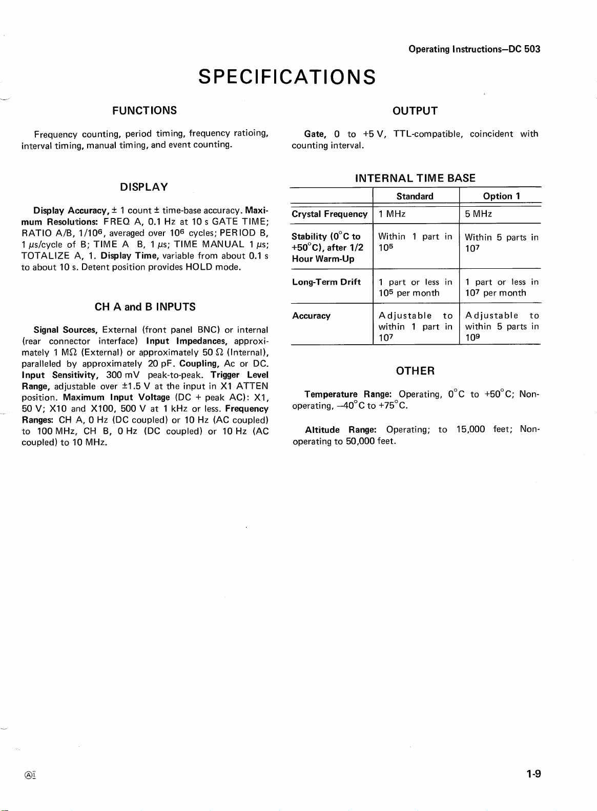
5;PECIFlCATlONS
FUNCTIONS
DISPLAY
CH A and
OUTPUT
-Time Base
nstallation
nput Sources
StartIStop
B
B
Intervals
I10
INPUTS
Page SECTION 1 OPERATING INSTRUCTIONS (cont)
INTERNAL TlME BASE
OTHER
SECTION
SECTION
2
THEORY OF OPERATION
INPUT CIRCUIT
Attenuators, Channels A and
Signal Shaping and Slope Channels
A and
DCU Signal Selection Gates
Time
TlME BASE AND CONTROL CIRCUITS
1
Optional
Decade Divider Units
Gate Generator
COUNTER CIRCUITS
Decade Counter Units
Storage Register
Overflow Register and Drive
DECODE AND DISPLAY MULTIPLEX
Scan Clock
+8
Seven-Segment Decoder and Driver,
Leading Zero Suppression
lnput and Output Data Lines
REGULATED POWER SUPPLIES
3
SERVICE INFORMATION
Symbols and Reference Designators
Electrical Parts List
Internal Adjustment Procedure
Controls and Connectors Illustration
Block Diagram
Parts Location Grid
Trigger Amplifier Diagram
Counter Time Base and Control
Counters and Display Diagram
Mechanical Parts List
Fig.
Accessories and Repackaging
(B)
A
B (A Start-B Stop)
MHz Clock
1
MHz Clock
Counter and Time-Slot Decoder
and Display and Parameter
Diagram
1
Exploded View
(B)
(DDU's)
(DCU)
LED'S
.
Page
Page 4
Page 5
Section
1-DC
503
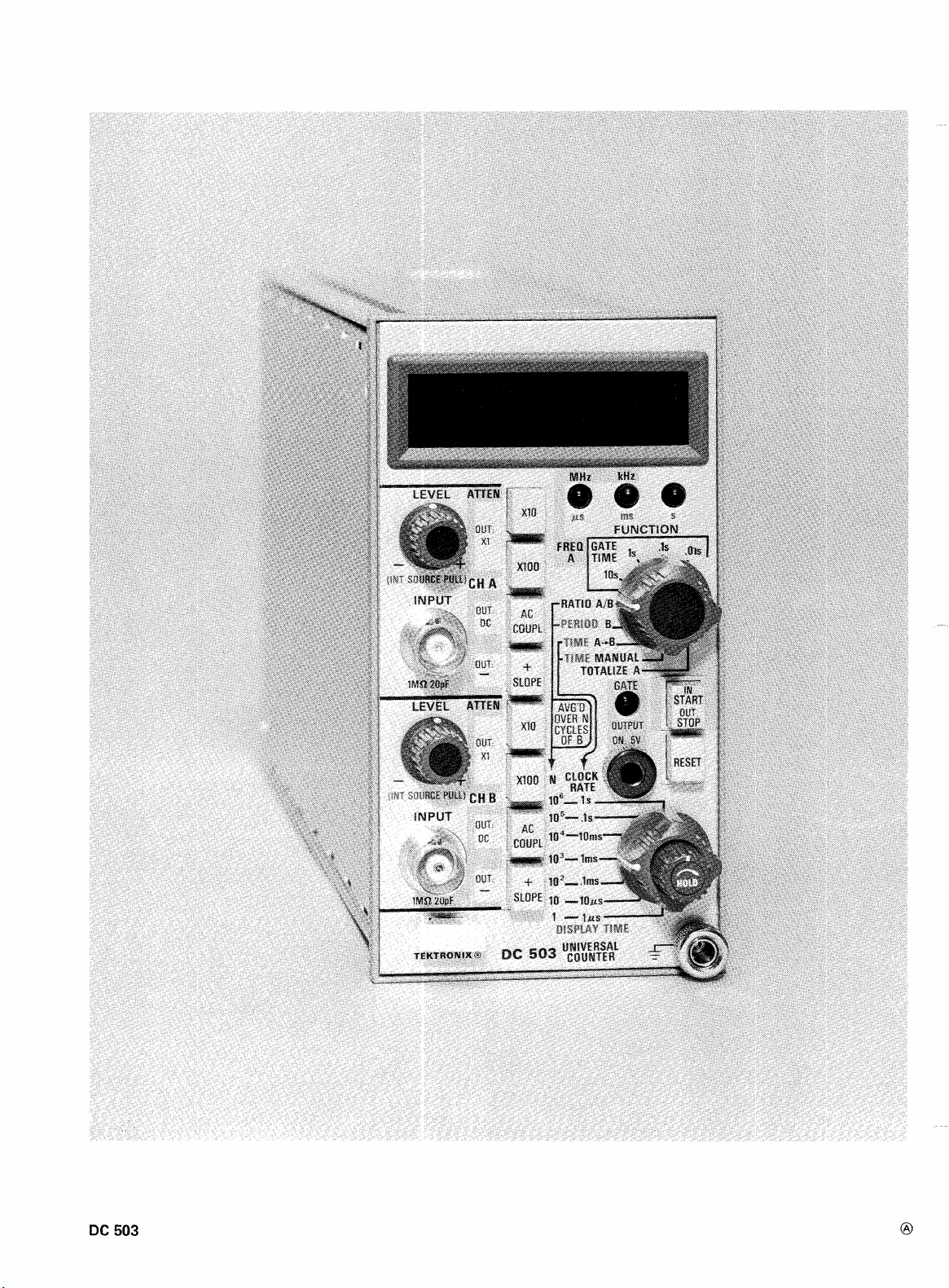
INTRODUCTION
Description
The DC 503 Universal Counter has six measurement
functions:
period timing, interval timing, manual timing, and event
counting.
The DC 503 operates in TEKTRONIX TM 500 Series
Power Modules only.
a multiple-compartment Power Module. The DC 503 is
fully compatible with other members of its digital measurement family.
The DC 503 has two channels
inputs and separate triggering level, attenuators, and
coupling mode controls. CH
CH
devices
positioned decimal point. Leading zeros to the left of the
frlequency counting, finding frequency ratios,
It
will operate in any compartment of
(A & B), each having BNC
A
has a 100 MHz capability,
B
10 MHz. Seven-segment LED numerical display
prov~ide 7-digit readout with an automatically-
SECTION
1
OPERATING
INSTRUCTIONS
most significant digit or the decimal point are blanked.
flashing display indicates register overflow.
Option
temperature-compensated, 5 MHz crystal oscillator to obtain a highly stable and precise internal time base. This
option includes
1 MHz clock.
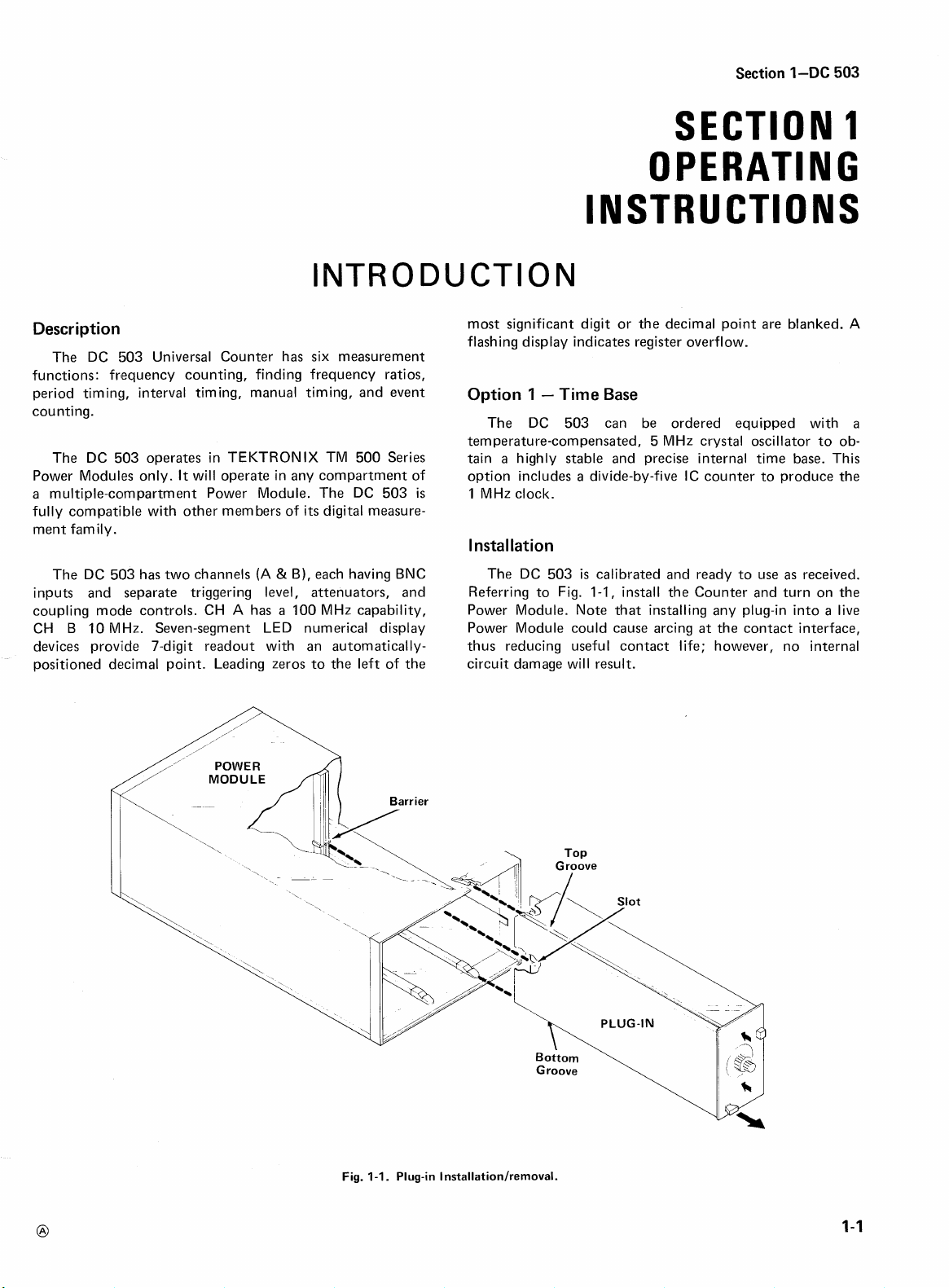
l nstallation
Referring to Fig. 1-1, install the Counter and turn on the
Power Module. Note that installing any plug-in into a live
Power Module could cause arcing
thus reducing useful contact life; however, no internal
circuit damage will result.
1
-
Time Base
The DC 503 can be ordered equipped with a
a
divide-by-five IC counter to produce the
The DC 503
is
calibrated and ready to use as received.
at
the contact interface,
A
Fig.
1-1.
Plug-in Installation/removal.
Page 6
Operating Instructions-DC
503
OPERATIONAL CHECK
Controls and Connectors
Pull out the tab labeled "Controls, Connectors, and
Adjustments" (at the rear of the manual) to expose the
front
ane el
illustration. Review the functions of the
controls, connectors, and indicators before continuing with
the operational checks.
Display Tests
With no signal applied,
displays and switching logic. The following checks will
most of the Counter's major circuits and ensure
readiness to make measurements. If any malfunctions are
detected, first refer to the Adjustment Procedure in the
Service section of this manual, then the System Mainte-
nance section of the Power Module manual.
Readout Segment Test.
check the seven character segments of each digit. A row of
8's should be displayed. This check of the display devices
and drivers can be done at anv time.
FREQ A Displays.
FREQ A GATE TlME of
location, leading zero suppression, and units indicators
according to Table
Using the FUNCTION switch, select a
1-1.
test
the DC 503's readout
Press the RESET button to
.O1
s.
Check the decimal point
TABLE
1-1
Decimal Point
.oooo
.00000
test
its
TABLE
NICLOCK RATE Switch
106
105
1 04
I
03
The GATE and units indicators should remain off.
PERIOD B Displays.
PERIOD B and the NICLOCK RATE switch to
the readout display according to Table
TABLE
NICLOCK RATE Switch 1 Units Indicator 1 Decimal Point
1
10
1 02
I
03
I
04
I
05
1
06
TlME AtB Displays.
TlME
A+B and the NICLOCK RATE switch .to
the readout displays according to Table
1-2
I
Decimal Point
.000000
.OOOOO
.OOOO
.ooo
Set the FUNCTIOIV Switch to
1.
Check
1-3.
1-3
ms
ms
ms
PS
PS
PS
PS
Set the FUNCTION switch to
.ooo
.oooo
.00000
.ooo
.oooo
.ooooo
.000000
1
s.
Check
1-4.
-
10
s
With the DISPLAY TlME control in the full ccw
position, observe that the GATE indicator flashes rapidly
for short GATE
TIMEs. Using a short GATE TIME, rotate the DISPLAY
TlME control slowly cw. Observe that the GATE light will
stay off for a longer and longer time, until the control
clicks into the HOLD detent position, holding off the
GATE indefinitely. Return the DISPLAY TlME control to
the ccw position.
RATIO A/B Displays.
RATIO A/B and the NICLOCK RATE switch to
Check the readout display according to Table
TIMEs and more slowly for longer GATE
kHz
Set the FUNCTION switch to
.OOOO
106.
1-2.
TABLE
NICLOCK RATE Switch
I
s
TIME MANUAL Displays.
TlME MANUAL and the NICLOCK RATE switch to
Check the readout display according to Table
1-4
Units lndicators
S
Set the FUNCTION switch to
Decimal Point
1-5.
0
-
1
ps.
Page 7
Operating Instructions-DC
503
TABLE
NICLOCK
The GATE: light should turn on and an advancing count
should be diisplayed when the
pushed in. The GATE light should turn off when the count
is
stopped by releasing the STARTISTOP button. Test the
overflow display by setting NICLOCK RATE to
pressing START, letting the count advance until the last
decade (seventh digit) reaches
flash. Release the START button and observe that the
display
RESET clears the overflow condition, sets the count to
zero, and
RATE
Switch Units Indicators Decimal Point
still
flashes but the numbers do not change. Pressing
stops the flashing display.
1-5
ms
STARTISTOP button
9
and the display begins to
.ooo
I
ps,
is
TOTALIZE A
TOTALIZE A. Observe
display. The GATE light should turn on when the START
button
The units indicators should remain off.
Channels
the attenuators, can be checked in a no-signal-input
condition by generating psuedo-triggers with the LEVEL
controls.
other channel. Set FUNCTION to
CLOCK RATE to 1 ms. Rotate CH A LEVEL back and
forth through
on. Rotate CH B LEVEL back and forth through
selected slope until the GATE light turns off. The resultant
display
events.
method, consult the Service section of the manual for
troubleshooting aids.
is
pushed in, and turn off when START
A & B
The channel A & B input circuits, with the exception of
Select
+
is
If the GATE light cannot be turned on or off with this
Display. Set the FUNCTION switch to
a
zero
at
the right of the readout
is
released.
SLOPE for one channel and - SLOPE for the
TIME A-tB and NI
its
selected slope until the GATE light turns
its
the time interval between these two trigger
INPUT CONSIDERATIONS
l
nput Sourc:es
The switch] concentric with the LEVEL control of each
channel selects either the front-panel BNC connector
(external), or the rear interface connector (Internal) pins;
Channel A via pin
The External inputs present high impedances of approximately 1
input circuits; present nominal 50
typical coaxial cable signal connections.
ML2, paralleled by about 20 pF. The Internal
lnput Coupling
Front Panel pushbuttons select AC (Capacitive) or DC
(Direct) coupling for each channel's input signal. This
coupling takes place
selected
attenuators of each channel.
soulrce and before they are passed on to the
16A, and Channel B via pin 17B.
Q
impedances to match
after the signals arrive from the
Attenuators and Maximum lnput Volts
Both front-panel pushbuttons, when out, provide no
(XI
).
attenuation to the input signal
maximum safe input voltage
the frequency limit of each channel. With either the
XI 00 attenuator selected (buttons are self-cancelling), the
maximum safe input voltage
1 kHz or
less.
is
50 V (DC + peak AC), up to
is
500 V (DC + peak AC)
In this mode, the
XI0 or
Sensitivity and Frequency Range
CH A will respond to signal amplitudes of
mV, peak-to-peak, up to 100 MHz.
300
CH B will respond to signal amplitudes of at least
mV, peak-to-peak, up to 10 MHz.
300
Depending on the coupling mode selected, the low
is
frequency limit for each channel
coupled) or 10 Hz (AC-coupled).
either 0 Hz (DC-
at
least
at
Page 8
Operating Instructions-DC
503
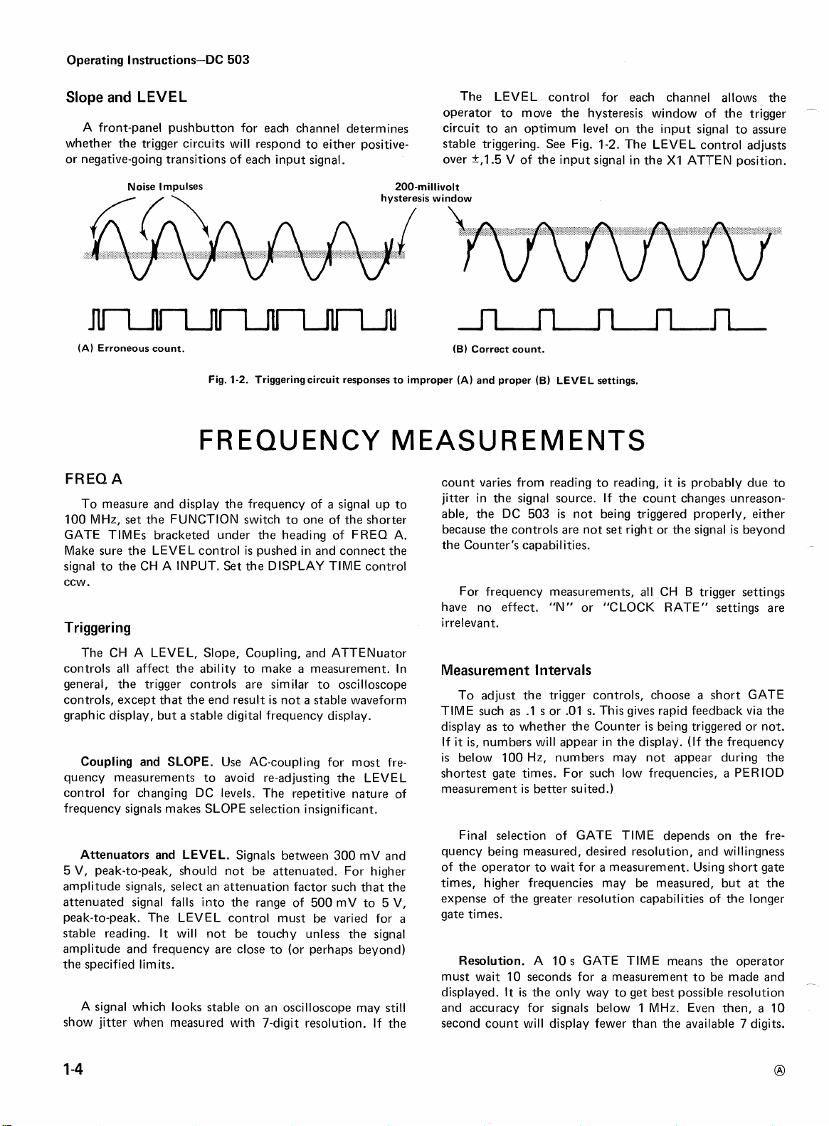
Slope and
A front-panel pushbutton for each channel determines
whether the trigger circuits will respond to either positive- stable triggering. See Fig.
or negative-going transitions of each input signal. over
(A)
LEVEL
Noise Impulses 200-millivolt
Erroneous count.
Fig.
1-2.
Triggeringcircuit responses to improper
hysteresis window
The LEVEL control for each channel allows the
operator to move the hysteresis window of the trigger
circuit to an optimum level on the input
+,I
.5
V of the input signal in the
(6)
Correct count.
(A)
and proper
(B)
LEVEL settings.
FREQUENCY MEASUREMENTS
FREO
100
GATE TIMEs
Make sure the LEVEL control
signal to the CH A INPUT. Set the DISPLAY TlME control
CCW.
Triggering
A
To measure and display the frequency of
MHz, set the FUNCTION switch to one
bracketed
under
the
heading
is
pushed in and connect the
a
signal up to
of
the shorter
of
FREO
A.
count varies from reading to reading,
jitter in the signal source. If the count changes unreasonable~
the
DC
503
is
not being triggered prc)per'yr either
because the controls are not set right or the signal
the
For frequency measurements, all CH B trigger settings
have no effect. "N" or "CLOCK RATE" settings are
irrelevant.
capabilities.
signal to assure
1-2.
The LEVEL control adjusts
XI
ATBEN position.
it
is
probably due to
is
beyond
The CH A LEVEL, Slope, Coupling, and
controls all affect the ability to make a measurement. In
general, the trigger controls are similar to oscilloscope
controls, except that the end result is not a stable waveform
graphic display, but a stable digital frequency display.
Coupling and
quency
control for changing DC levels. The repetitive nature of
frequency signals makes SLOPE selection insignificant.
5
amplitude signals, select an attenuation factor such that the
attenuated signal
peak-to-peak. The LEVEL control must be varied for a
stable reading.
amplitude and frequency are close to (or perhaps beyond)
the specified limits.
show jitter when measured with 7-digit resolution. If the
measurements
Attenuators and
V, peak-to-peak, should not be attenuated. For higher
A signal which looks stable on an oscilloscope may still
SLOPE.
falls into the range of
It
will not be touchy unless the signal
Use AC-coupling
to
avoid re-adjusting the LEVEL
LEVEL.
Signals between
ATTENuator
for
most
300
500
mV to 5 V,
fie-
mV and
Measurement Intervals
To adjust the trigger controls, choose a short GATE
TlME such as
display as to whether the Counter is being triggered or not.
If
it
is, numbers will appear in the display. (If the frequency
is below
shortest gate times. For such low frequencies, a PERIOD
measurement
Final selection of GATE TlME depends on the
quency being measured, desired resolution, and willingness
of the operator to wait for a measurement. Using short gate
times, higher frequencies may be measured, but at the
expense of the greater resolution capabilities of the longer
gate times.
Resolution.
must wait
displayed.
and accuracy for signals below
second count will display fewer than the available 7 digits.
.I
s
or
.O1
s.
This gives rapid feeldback via the
100
HZ, numbers may not appear during the
is
better
suited-)
A
10
s
GATE TlME means the operator
10
seconds for a measurement to be made and
It
is
the only way to get best possible resolution
1
MHz. Even then, a
fre-
10
-
Page 9
Operating Instructions-DC
503
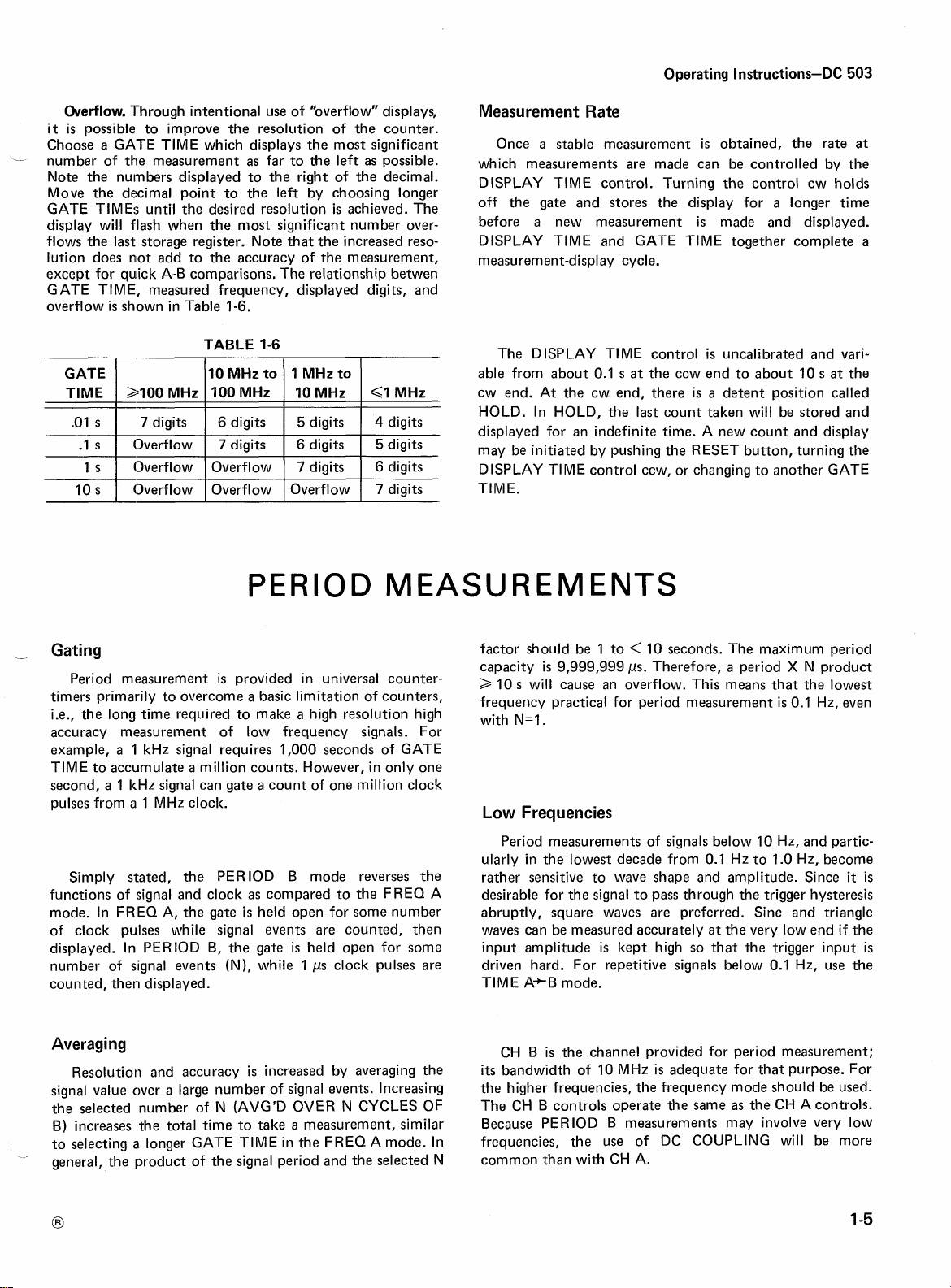
Overflow.
it
is
Choose
-
number of the measurement as far to the left
Note the
Move the decimal point to the left by choosing longer
GATE TIME!; until the desired resolution
display will flash when the most significant number over-
flows the
lution does
except for quick A-B comparisons. The relationship
GATE TIME, measured frequency, displayed digits, and
overflow
:EF
10
Through intentional use of "overflow" displays,
possible to improve the resolution of the counter.
a
GATE TlME which displays the most significant
numbers displayed to the right of the decimal.
is
achieved. The
last
storage register. Note that the increased reso-
not add to the accuracy of the measurement,
is
shown in Table 1-6.
TABLE
10
1
2100
MHz
100
;
1
7
digits
(3verflow
(3verflow Overflow
s
Overflow Overflow Overflow
1
MHz
MHz
6 digits
7
digits
1-6
1
MHz
to
,
10
MHz
1
5
digits
6
digits
7
digits 6 digits
to
as
possible.
betwen
hl
MHz
1
4
digits
5
digits
7
digits
Measurement Rate
Once a stable measurement
which measurements are made can be controlled by the
DISPLAY TlME control. Turning the control cw holds
off the gate and stores the display for
a
before
DISPLAY TlME and GATE TlME together complete
measurement-display cycle.
The D
able from about 0.1
cw end. At the cw end, there
HOLD. In HOLD, the
displayed for an indefinite time. A new count and display
may be initiated by pushing the RESET button, turning the
DISPLAY TlME control ccw, or changing to another GATE
TIME.
new measurement
ISPLAY TI ME control
s
at
the ccw end to about 10
last
is
obtained, the rate
a
longer time
is
made and displayed.
is
uncali brated and vari-
is
a
detent position called
count taken will be stored and
at
s
at
the
a
PERIOD MEASUREMENTS
-
Gating
is
Period measurement
timers primarily to overcome a basic limitation of counters,
i.e., the long time required to make a high resolution high
accuracy measurement of low frequency signals. For
example, a 1 kHz signal requires 1,000 seconds of GATE
TlME to
second, a 1 kHz signal can gate
pulses from a 1 MHz clock.
functions of signal and clock as compared to the FREQ A
mode. In FREQ A, the gate
of clock pulses while signal events are counted, then waves can be measured accurately at the very low end if the
displayed. In PERIOD B, the gate
number of signal events (N), while 1 ps clock pulses are
counted,
Averaging
signal value over
the selected number of N (AVG'D OVER N CYCLES OF
B) increases the total time to take
to selecting
general, the product of the signal period and the selected N
acc~~mulate a million counts. However, in only one
Simply stated, the PERIOD B mode reverses the rather sensitive to wave shape and amplitude. Since
then displayed.
Resolutiori and accuracy
a
large number of signal events. Increasing
a1
longer GATE TlME in the F REQ A mode. In
provided in universal counter-
a
count of one million clock
is
held open for some number abruptly, square waves are preferred. Sine and triangle
is
held open for some
is
increased by averaging the
a
measurement, similar
factor should be 1 to < 10 seconds. The maximum period
capacity
frequency
with
Low
ularly in the lowest decade from 0.1 Hz to 1.0 Hz, become
desirable for the signal to pass through the trigger hysteresis
input amplitude
driven hard. For repetitive signals below 0.1 Hz, use the
TIME A*B mode.
its
the higher frequencies, the frequency mode should be used.
The CH B controls operate the same
Because PERIOD
frequencies, the use of DC COUPLING will be more
common than with CH A.
is
9,999,999
will
cause
practical
N=~.
Frequencies
Period measurements of signals below 10 Hz, and partic-
CH
B
is
the channel provided for period measurement;
bandwidth of 10 MHz
ps.
Therefore, a period X N product
an
overflow.
for
period
is
kept high so that the trigger input
B
measurements may involve very low
This
means
that
measurement
is
adequate for that purpose. For
is
O.l
as
the CH A controls.
the
lowest
Hz,
even
it
is
is
Page 10
Operating Instructions-DC
503
RATIO MEASUREMENTS
In the RATIO A/B mode, the frequency of the signal
applied to CH A
applied to CH B, and the resultant ratio
that the normal "frequency" mode
is
divided by the frequency of the signal may be desirable to set the trigger controls independently.
is
displayed. Note This may be accomplished
is
basically a ratio
mode, in which the ratio of the unknown signal to the
internal clock
is
displayed. (Decade scaling of the internal
clock and decimal point positioning normalizes the display
relative to kHz or MHz units.)
Bandwidth Limitations
Because CH B has
feasible to make ratio measurements of two signals, both
well above
10
somewhat above
applied.
a
bandwidth of only
MHZ.
ow ever,
10
MHz if adequate signal amplitude
CH B will respond to signals
10
MHz,
it
is
not
Triggering
The operation of CH A and CH B trigger controls
same
as
for frequency and period measurement. In fact, digits will be best.
is
the
TIME INTERVAL MEASUREMENTS
since both channels must be triggered to obtain
as
follows:
1
)
Go to the FREQ A mode and adjust the CH A trigger
controls
for
a
normal
frequency
2)
Go to the PERIOD B mode and adjust the CH B
measurement.
trigger controls for a normal period measurement.
Leaving CH A and CH B trigger controls
3)
go
to
is
be
displayed.
the RATIO A/B mode. The correct ratio should
The NICLOCK RATE control may now be operated to
select maximum resolution. For most measurements, the
smallest value of "N" which produces
a
useful number of
a
display,
as
it
they
Electronic Startlstop
TlME A*B mode measures and displays the elapsed
The
time
interval
subsequent triggering of CH B. The triggering event does
not have to be the same one for both channels. Separate
events do not even have to be time related.
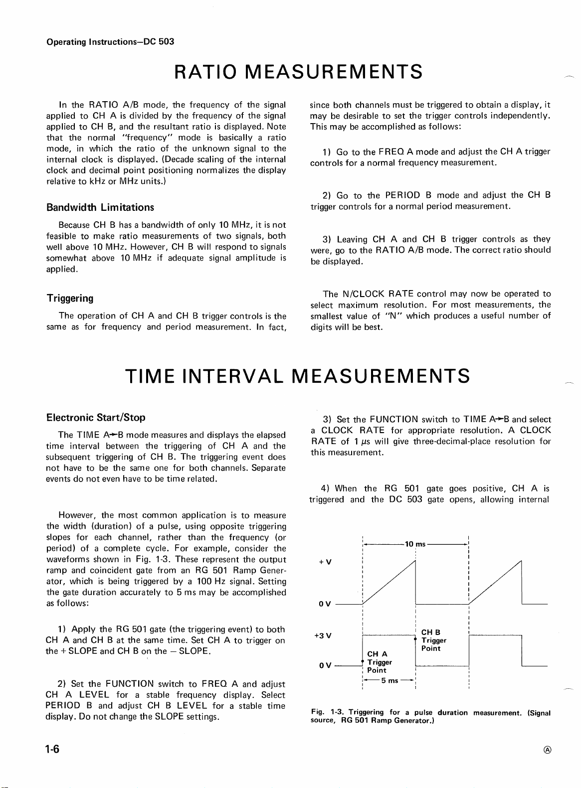
However, the most common application
the width (duration) of
slopes for each channel, rather than the frequency (or
period) of
waveforms shown in Fig.
ramp and coincident gate from an RG
ator, which
the gate duration accurately to
as
follows:
1)
Apply the RG
A
and CH B at the same time. Set CH A to trigger on
CH
the
+
SLOPE and CH B on the - SLOPE.
2)
Set the FUNCTION switch to FREQ A and adjust
CH A LEVEL for a stable frequency display. Select
PERIOD B and adjust CH B LEVEL for a stable time
display. Do not change the
between
a
complete cycle. For example, consider the
is
being triggered by
the
triggering
a
pulse, using opposite triggering
1-3.
These represent the output
5
501
gate (the triggering event) to both
SLOPE
of
CH
A
is
to measure
501
Ramp Gener-
a
100
Hz signal. Setting
ms may be accomplished
settings.
and
the
3) Set the FUNCTION switch to TIME A-+B and select
a
CLOCK RATE for appropriate resolutior~. A CLOCK
RATE of
I
ps
will give three-decimal-place resolution for
this
4)
When the RG
triggered and the DC
I
I
I
I
+3
v
CH
"
ov
Fig.
1-3.
source, RG
Trigger
I
Point
/-5ms-;
I
Triggering for a pulse duration measurement. (Signal
501
Ramp Generator.)
501
gate goes positive, CH A
503
gate opens, allovving internal
I
I
I
I
'
CHB
"
Trigger
A
Point
I
I
I
I
I
I
I
is
Page 11
Operating Instructions-DC
503
clock pulses .to be counted. When the RG 501 gate starts to
is
return to zero, CH B
and the
-
operator can adjust the RG 501 controls until the required
accuracy
accurnulated count of clock pulses
5) If the count
is
ac:h ieved.
triggered, the DC 503 gate closes,
is
displayed.
is
off the desired time interval, the
Single-Shot Using HOLD
Single-shot time intervals can be measured by putting
the
DISPLAY TlME control in HOLD. This will lock out
MANUAL TIMING MEASUREMENTS
The TlME MANUAL position
TlME
CLOCK RATE switch and
display.
A+B electronic mode. In this mode, only the
Starting antl Stopping
The TIME MANUAL mode may be thought of
"stop-watch" type of operation. With the FUNCTION
switch in the TlME MANUAL position, the display starts
counting time-base pulses when the
pressed.
lated total
last
START command
again advance), or other controls are actuated. Pushing
RESET will return the display to zero. Changing the setting
It
wnll continue to count and display the accumu-
until the STARTISTOP button
count will then be held in the display until another
is
given (in which case the count will
is
a
manual analog of the
STARTISTOP switch affect the
STARTISTOP button
is
released. The
as
both channels after CH A and CH B have been triggered,
respectively. Pushing RESET clears the display and re-arms
the trigger channels for another measurement.
GATE
front-panel GATE OUTPUT jack. Since
with the time interval measurement,
oscilloscope to graphically relate the digital measurement to
the analog signal.
of the CLOCK RATE switch will change the frequency of
the time-base pulses being counted, and return the display
to zero.
Output
The internal gate of the DC 503
it
is
available
it
may be used with an
Clocking Rate
When the CLOCK RATE switch
one-second pulses are being counted, and the display
a
accumulation advances one count per second, and so on.
On the 1
one million counts per second.
is
9,999,999, the display will flash to indicate overflow;
however, the accumulation continues at the normal rate,
except that the digits for decades above
displayed.
ys position, the count accumulates
Whenever the accumulated count
is
in the
is
at
the
is
coincident
1
s
position,
at
the rate of
greater than
107 are not
TOTALIZING
Purpose
In the TOTALIZE A mode, signal
A INPUT
displayed during the time the STARTISTOP button
pushed in. This mode
mode.
relatively infrequent and irregular events.
a~re counted and the accumulated total
is a manual analog of the frequency
It's
main application
is
Operation
Apply the signal to CH A and set the trigger controls the
same as for frequency measurement.
Starting tlie Count.
and adjust the CH A LEVEL control until
Press the STARTISTOP button in
events
applied to CH
to accumulate a count of
a
count begins to
is
is
The
advance.
numbers. Only the CH A trigger controls, the RESET
button, and the
Stopping the Count.
released and no other controls are operated, the
will continue to be displayed. No more incoming events will
be added to the total.
Restarting and Resetting.
depressed, incoming events will advance the displayed total.
Resetting the count to zero can be done at any time by
pressing the RESET button or by moving the FUNCTION
switch to some other position, then back to TOTALIZE A.
accumulated count
STARTISTOP button affect the display.
If the STARTISTOP button
is
displayed in whole
When the START
last
is
is
total
again
Page 12
Operating Instructions-DC
503
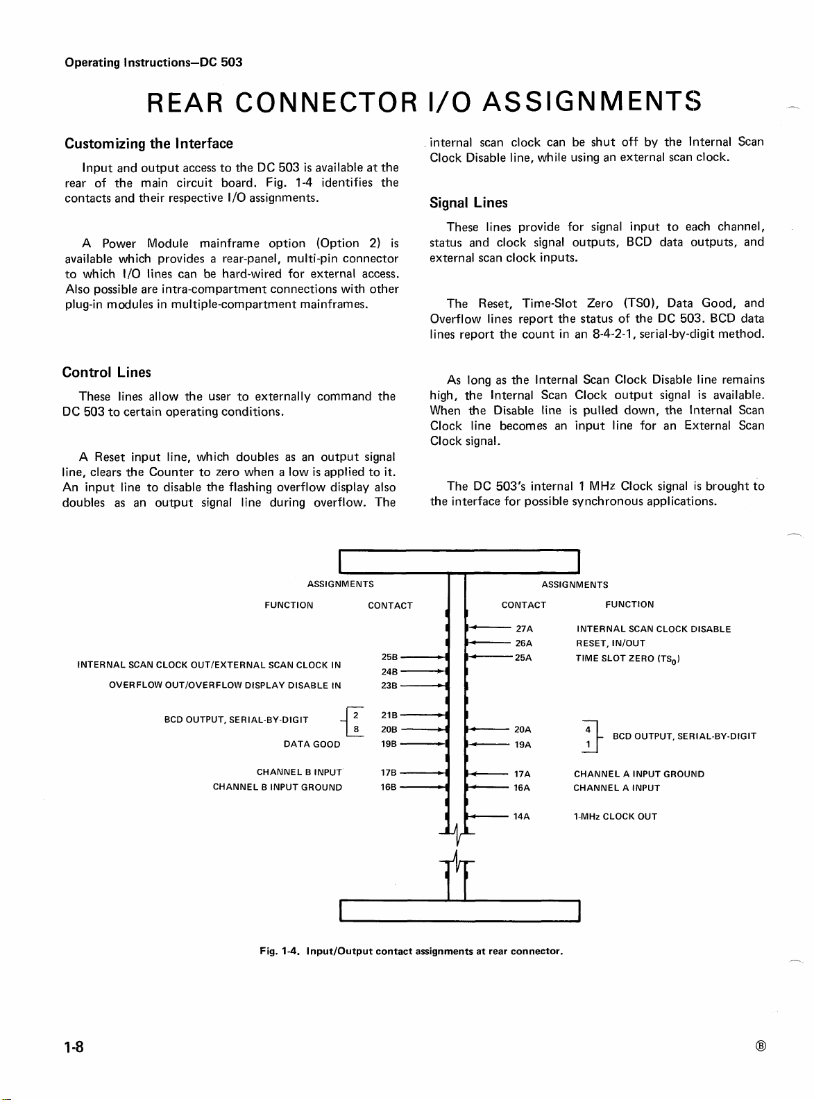
REAR
Customizing the Interface
Input and output access to the DC 503
rear of the main circuit board. Fig. 1-4 identifies the
contacts and their respective
A Power Module mainframe option (Option 2)
available which provides
to which
Also possible are intra-compartment connections with other
plug-in modules in multiple-compartment mainframes. The Reset, Time-Slot Zero
Control Lines
These lines allow the user to externally command the
DC
A Reset input line, which doubles
line, clears the Counter to zero when a low
An input line to disable the flashing overflow display also
doubles as an output signal line during overflow. The the interface for possible synchronous applications.
If0 lines can be hard-wired for external access.
503
to certain operating conditions.
CONNECTOR I/O ASSIGNMENTS
.
internal scan clock can be shut off by the Internal Scan
is
available at the
I10 assignments.
a
rear-panel, multi-pin connector
as
an output signal
is
applied to
it.
Clock Disable line, while using an external scan clock.
Signal Lines
These lines provide for signal input to each channel,
is
status and clock signal outputs, BCD data outputs, and
external scan clock inputs.
(TSO), Data Good, and
Overflow lines report the status of the DC 503. BCD data
lines report the count in an 8-4-2-1, serial-by-cligit method.
As long as the Internal Scan Clock Disable line remains
high, the Internal Scan Clock output signal
When the Disable line
Clock line becomes an input line for an External Scan
Clock signal.
The DC 503's internal
is
pulled down, the Internal Scan
1
MHz Clock signal
is
iis
available.
brought to
INTERNAL
OVERFLOW
SCAN
CLOCK
OUTIEXTERNAL
OUTIOVERFLOW
BCD
OUTPUT,
SERIAL-BY-DIGIT
CHANNEL B INPUT
FUNCTION
SCAN
DISPLAY
CHANNEL
Fig.
I
ASSIGNMENTS
CONTACT
I
I
1-
-
{
25B
24B
23
:::
19B
17B
16B
B
-1
CLOCK
IN
DISABLE
DATA
1-4.
IN
GOOD
B
INPUT
GROUND
InputIOutput contact assignments at rear connector.
4
+I
4
d
-
I
I
-
-
I
-
I
-
I
I
ASSIGNMENTS
FUNCTION
27A
26A
25A
20A
19A
17A
16A CHANNEL A INPUT
14A
INTERNAL
RESET,
TIME
SLOT
CHANNEL
1-MHz
CLOCK
SCAN
INIOUT
ZERO
BCD
OUTPUT, SERIAL-BY-DIGIT
A
INPUT
OUT
CLOCK
(TS,)
GROUNID
CllSABLE
Page 13
Operating Instructions-DC
503
SPECIFICATIONS
+
FUNCTIONS
OUTPUT
Frequency counting, period timing, frequency ratioing,
interval timing, manual timing, and event counting.
DISPLAY
Display Accuracy,
Resolultions:
mum
RATIO
1
TOTALIZE
to about 10
(rear
mately 1
paralleled by approximately 20
l
Range,
position.
50 V; XI0 and X100, 500 V
Ranges:
to 100 MHz, CH
coupled) to 10 MHz.
A/B, 1/106, averaged over 106 cycles; PERIOD B,
ps/cycle of 6; TlME A B, I ps; TlME MANUAL I ps;
A,
s.
Signal Soi~rces,
connecitor interface)
MQ (External) or approximately 50 Q (Internal),
nput Sensit:ivity,
adjustable over
Ma:~imum Input Voltage
CH
,A,
+
1
count f time-base accuracy.
FREQ A, 0.1 Hz at 10 s GATE TIME;
1.
Display Time,
Detent position provides HOLD mode.
CH A
and
External (front panel BNC) or internal
300 mV pea k-to-pea k.
+I
0 Hz (DC coupled) or 10 Hz (AC coupled)
6, 0 Hz (DC coupled) or 10 Hz (AC
variable from about 0.1
B INPUTS
l nput Impedances,
pF.
Coupling,
.5 V
at
the input in XI ATTEN
(DC + peak AC): XI,
at
1 kHz or less.
approxi-
Ac or DC.
Trigger Level
Frequency
Maxi-
Gate,
counting interval.
Crystal Frequency
Stability
+50°c), after
s
Hour Warm-Up
Long-Term Drift
Accuracy
operating to 50,000 feet.
(O'C to
Temperature Range:
Altitude Range:
0 to +5 V, TTL-compatible, coincident with
INTERNAL TIME BASE
1 MHz
Within 1 part in
112
105
1
part or less in
1 05 per month
Adjustable to
within 1 part in
I
07
Standard
Option
5 MHz
Within 5 parts in
1 07
1
part or
107 per month
Adjustable to
within 5 parts in
I
09
1
less
in
OTHER
-400C
Operating,
+750c-
Operating; to 15,000 feet; Non-
OOC
to +50°c; Non-
Page 14

Page 15
Section
2-DC
503
INPUT
Attenuators, Channels A and (B)
Events to be counted are applied via front-panel INPUT
connector
are frequency-compensated voltage dividers consisting of
resistors R 18-R25
(C118-C125). Switches S20A (S120A) and S20B (S120B)
allow front-panel selection of XI, X10, or XI00 attenuation of
coupling.
J10 (J110) to the attenuators. The attenuators
(R 1 18-R 125) and capacitors C18
the input signal. C15 (C115) provides AC
SECTION
THEORY
OPERATION
CIRCUIT
DCU Signal Selection Gates
The two separate bistable multivibrators produce sharp
signal edges for the decade counter units
TOTALIZE A, RATIO
positions,
and
MANUAL, or TlME
bistable multivibrator for the DCU drive and
by the DDU (decade divider unit) output. In PERIOD
U200D-U226C
control signal from the 1 MHz clock.
U200A-U200C
is
switched
by the channel A input signal. In TlME
is
AIB, or one of the FREQ A
is
the active bistable multivibrator
A-tB, U200D-U226C
the active multivibrator.
OF
(DCU). In
is
the active
is
controlled
It
receives
2
B,
a
Signal Shaping and Slope, Channels A and (B)
Field effect transistor (FET) 035 (0135) presents a high
impedance
base of
between the LEVEL control R45
050 (0150). Adjustment of the LEVEL control changes
the bias on
the input signal will trigger the DC 503.
060 and 1050 in the Channel A signal shaping circuitry
comprise
in the Channel B signal shaping circuitry) acts
follower.
070-080 (0160-0170)
pair.
slope by biasing the desired slope to R74
positive slope
negative slope
follower 095
and the slope-determined output signal to the appropriate
DCU signal selection gate and the A start portion of the
Time
to1 the input signal and a low impedance to the
050 (01 50). FET 040 (0140) provides isolation
(R145) and the base of
(150 (0150) and thus selects what portion of
a
hiigh frequency, high gain amplifier. 068 (0150
as
an emitter
is
a
signal switched differential
+
SLOlPE switch S75 (S170) selects the triggering
(R165). The
is
passed through 090 (0165), while the
is
passed through 074 (0180). Emitter
(0185) couples the signal level to a TTL level
A+B ciircuit.
The output signal from the active bistable multivibrator
goes to NOR gate
toggle the decade counter units.
U200B. The output of U200B
is
used to
Time A+B (A Start-B Stop)
The two separate bistable multivibrators (U220C-U220D
and U220A-U220B) produce sharp edges to toggle U224A
and B.
In TlME
at
pin 1 of U226A, making pin 3 of NAND gate U226B
high. Pin 4 of U226B starts low when
pin 4 of U224A. Pin 5 of U226B starts high due to a low
pin 13 of U224B. An "A trigger" causes U224A to toggle,
which makes pin 4 of
pin 14 of
of event to be counted).
"armed" by the high that occurs
circuit now waits for a "B trigger" which will toggle
and put a low on pin 5 of U226B. When the B trigger
arrives,
gate generator circuit closing the gate. When the gate closes,
a CLEAR resets
A+B mode the FUNCTION switch puts a low
CLEAR
U226B high. This outputs a low to
U272B1 causing the gate to "open" (permits input
U224B simultaneously becomes
at
its
pins 12 and 13. The
U226B will output a high to pin 14 of U272B in the
U224A, which in turn resets U224B.
goes low
U224B
at
at
Page 16
Theory of Operation-DC
TIME BASE AND CONTROL CIRCUITS
503
1
MHz
Clock
A precise one-megahertz clock provides the reference for
FUNCTION switches and the DCU signal sele~ction gates to
the decade counter units.
operation of the gate-generating and time-counting circuits.
is
The output of crystal oscillator Y250
to exactly one megahertz. The four parts of U250
shaper-buffer stage to produce square-wave clock pulses and
to isolate the oscillator from the 1 MHz output line.
Optional 1 MHz
An optional 1 MHz clock
5 MHz crystal oscillator and
combination
Clock
is
available, using a very stable
a
divide-by-five counter. This
is
shown on the schematic as Y251 and U251.
Decade Divider Units (DDU's)
adjustable by C255
form
a
Signal
is
applied
to
pin
14
of
~260, whose
connected to the input of the subsequent tjecade. Each
The 1 MHz clock signal or Channel B shaped output
is
decade
clocked with a negative-going transition. The
DDU's are reset by a CLEAR pulse, which places
in U260 and a 9 count in each subsequent decade.
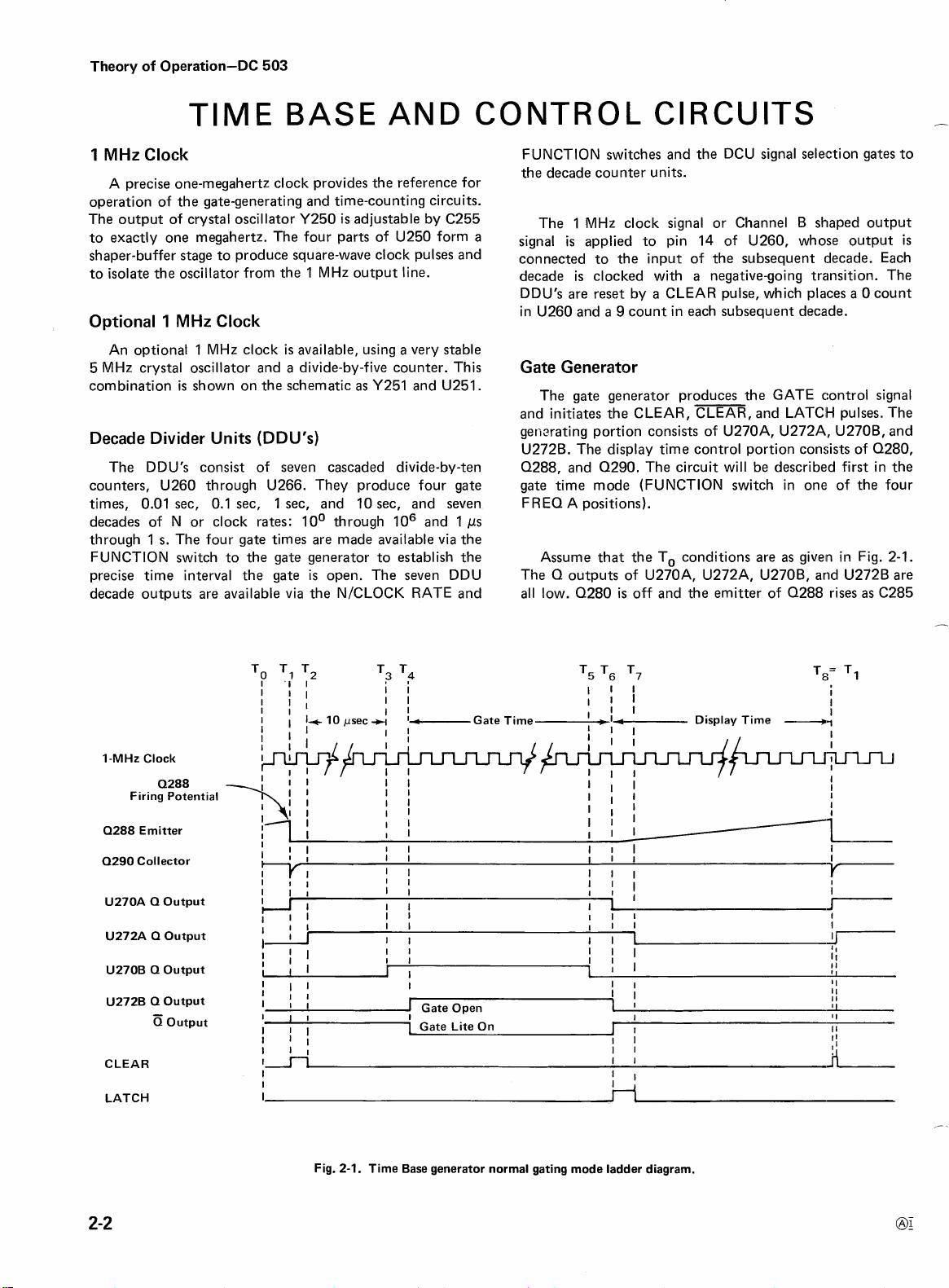
Gate Generator
The gate generator produces the GATE c:ontrol signal
and initiates the CLEAR, CLEAR, and
gerwrating portion consists of U270A, U272A, U270B, and
U272B. The display time control portion consists of 0280,
LATCH pulses. The
output
a
The DDU's consist of seven cascaded divide-by-ten 0288, and 0290. The circuit will be described first in the
counters, U260 through
times,
0.01 sec, 0.1 sec, I sec, and 10 sec, and seven FREQ A positions).
decades of N or clock rates:
through 1
s.
The four gate times are made available via the
FUNCTION switch to the gate generator to establish the
precise time interval the gate
decade outputs are available via the
U266. They produce four gate gate time mode (FUNCTION switch in one of the four
lo0
through
is
open. The seven DDU The 0 outputs of U270A, U272A, U270B, arid U272B are
NICLOCK RATE and all low. 0280
lo6
and I ps
Assume that the
is
off and the emitter of 0288 rises
To conditions are as given in Fig. 2-1.
0 count
as
C285
is
1-MHz Clock
Q288
Firing Potential
0288 Emitter
0290 Collector
U270A Q Output
U272A Q Output
U270B Q Output
U272B Q Output
-
Q Output
CLEAR
LATCH
T2
I II
I
11
I
II I I
I
I
I+
f
10 psec
I' I I
~+k!f.{i
I #I
I II
Ill I
lr
j
I'
I
!I
I
11
Ill I
)
;I
T
T
B?
I
I
I I
-tl
'-Gate Time-1- Display Time
I I Ill
I
I
I
I
1
I
I I
I I
I
I
I
I
I I Ill
I I
I
I
I
I
I
I
I
I I
I
I
1
I
I I I
1
Gate openc
1
Gate Lite On
T!5
T6 T7 TE;=
;I:
I
I
II
I
I
I
I
I
I
1;
I
I!'
111
ill
Ill
111
I
I~
'11
I I
LII
.I
I
I
I
I
++lnJ
-1
TI
I
I
I
I
I
1
I
i
I
I
7
I
7
I
I
j
i
I
I
I
I,
1
I
I I
I I
I
I
I
I
I
I
I
i
2-1. Time Base generator normal gating mode ladder diagram.
Fig.
Page 17
Theory of Operation-DC
503
charges. At TI, 0288 reaches
discharges the capacitor. This results in
pulse on the direct-set input (pin 2) of U270AI forcing
-
output high and
U280A,
high,
The next high-to-low transition from the 1 MHz clock
toggles U27i!A, causing
go low. With a low applied to one of
reverts to
and CLEAR pulses. The DDU's then start counting from
their 09999919 reset condition.
DDU's to count the first digit, plus
negative transition from the DDU's via either the FUNCTION or
mode) toggles
2-1.
next negative transition from the 1 MHz clock
U272B, causing
its
GATE indicator LED,
is
preventing
(GATE)
inverter and isolation transistor
.-
selected by either the FUNCTION or
switch (depending on operating mode). At the end of this
time, which corresponds to
transition from the DDU's toggles
its
produciing the CLEAR and CLEAR control signals.
At the
N1C:LOCK RATE switch (depending on operating
U270B1s Q goes high and
a
output .to go low (supplying current to the front-panel
applied to the base of Q280, saturating the tran~stor and
is
The GATlE remains open (high) for the time duration
its
a
output low. With two high inputs on
output goes low and the output of U280D goes
its
Q output to go high and
its
original condition, terminating the CLEAR
end of a 10-microsecond delay (time for the
U270B. This event corresponds to T3 in Fig.
its
Q output to go high (GATE open) and
DS275). The U272B Q output (gate)
C:285 from charging. The U272B Q output
also supplied to a front-panel connector via
its
firing potential and
a
short-duration low
its
inputs, U280A
a
propagation delay),
output goes low. The
its
(2278.
NICLOCK RATE
T5 in Fig. 2-1, another negative
U270B. U270B1s Q
its
(T,)
its
Eto
(T4) toggles
output goes low and
negative transition from the
Q
a
U272B1 causing
Simultaneously, the Q output goes high, removing current
from the GATE indicator LED.
When the
transition toggles
U280B has two high inputs, placing a low at the output of
U280B, terminating the LATCH signal.
The display time begins when the GATE signal ends
(T6). When 0280 turns off, C285 begins to charge through
R282-R285 toward the
TIME, provides an adjustable time constant to vary the
display time form about 0.1 second to about 10 seconds.
When the DISPLAY
(HOLD detent position), S285 opens, and C285 stops
charging. When S285
ciently to bring Q288 to
display time ends and the next GATE-opening sequence
begins.
Q270 provides an automatic reset by grounding the
RESET line for
FUNCTION and NICLOCK RATE switches also provide
method of automatic reset. The two switches ground the
RESET line between switch
matic reset insures that the readout has been cleared before
the next measurement. The automatic reset can be seen by
noting that the display goes to all eights (all LED segments
lit) in between switch detent positions.
U272B Q output goes low,
a
its
output goes high. The next
1 MHz clock (T6) toggles
its
Q-output to go low, closing the gate.
U270A, switching Q low and Q high. Now
Vcc
supply. R285, DISPLAY
TlME control
is
closed and C285 charges suffi-
its
firing potential (TI
short time after instrument turn-on. The
detent positions. The auto-
is
fully clockwise
the
negative
),
the
a
COUNTER CIRCUITS
Decade Counter Units (DCU)
The 100 through 106 DCU
ten counters. The first decade counter
J-E<
individual
circuit board,, to accept the high-speed decade input (up to
100 MHz),
U210B, U21:2, and U214 comprise the first (100) decade
counter, and U305 through
DCU1s.
six
When the J and K inputs of U210A are high (GATE
open), the counter
the toggle
counted by
goes low, providing
input for the second decade counter. Each subsequent
decade divides by ten in
output lines are connected from each DCU to
storage-register latch. When the CLEAR (high) and CLEAR
flip-flops, located on the Trigger Amplifier
and each subsequent DCU
is
enabled. The input signal is applied to
input of U210A. On every tenth clock input
the first decade counter, the output of U214
a
carry signal which becomes the clock
is
seven cascaded divide-by-
is
made up of four
is a single IC. U210A,
U310 make up the remaining
a
similar manner. Four BCD
its
associated
(low) signals are activated, all of the decade counters are
reset to the zero-count
state.
Storage Register
The seven IC latches (U320 through U326) comprise
storage register which stores the corresponding decade
counter BCD output. The BCD output number
the data inputs
bits respectively). The LATCH pulse
data-strobe input
(negative transition) or when the FUNCTION switch
placed in the TOTALIZE A, or TlME MANUAL positions.
While the LATCH input
inputs are transferred to the associated BCD bit output to
be scanned by the multiplexing circuit.
at
pins 1, 5, 7, and 3 (20, 21, 22, and 23
at
pin 2 of each latch
is
high, the logic levels
at
is
applied to
is
applied to the
the end of GATE
at
the data
is
Overflow Register and Drive
When the decade counters have counted to 9,999,999,
the counters are full. At the next count the
23 output of
a
Page 18

Theory of Operation-DC
U310 goes low, providing a toggle input to U311A. When
this occurs,
U311 A. When the LATCH pulse ends (goes low), U311
toggled and the high
U311 B goes high,
high now at the input of
which causes the LED display to flash.
a
high
503
is
transferred from pin 14 to pin 12 of
B
is
transferred to pin 8. When pin 8 of
CR311 and CR314 are turned off. The
U328B starts a multivibrator
U311A goes low on the first overflow count, 0312 and
of
CR314 turn off. Since pin 8 of U311B
off) by the clear input (pin 6), this first overflow count
is
causes
overflow circuit
the display
high).
a
flashing LED display. This difference in the
is
necessary in the "manual" modes, since
is
continuously read from the DCIJrs (LATCH
is
held high (CR311
-
In the
modes, overflow indication
CR314. The emitter of 0312
closure
TIME MANUAL and TOTALIZE A counting U311A
is
achieved via 0312 and leading-zero suppression during the overflow condition, the
is
grounded by a switch display-controlling circuits are notified via U328A that the
as
is
the clear input (pin 6) of U311
B.
When pin 13 count
is
reset by the CLEAR pulse. To prevent
is
in excess of that displayed by the LED readout.
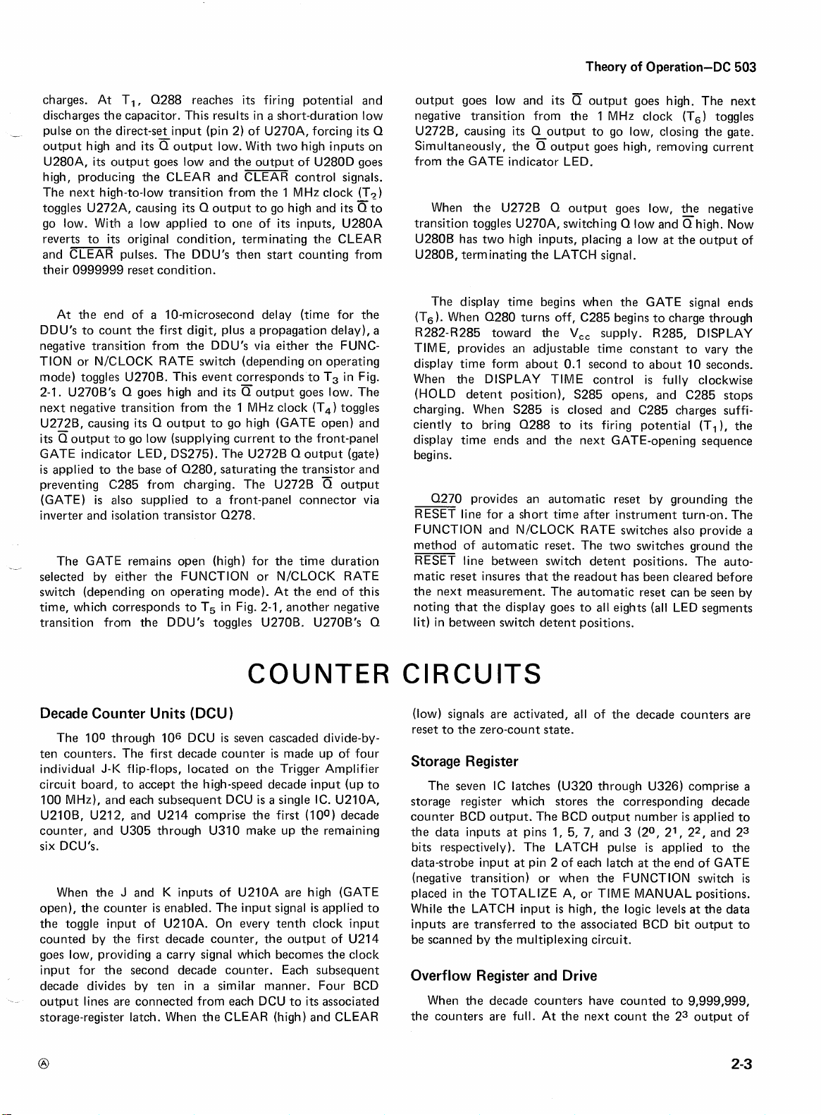
DECODE AND DISPLAY MULTIPLEX
Scan Clock
is
The scan rate of the multiplexing circuit
is
by the scan clock. The scan clock
and U330C, which operate
at an approximate 2-kilohertz rate.
provided for internal scan-clock disable, internal scan clock
output, and external scan clock input. The scan clock
output drives an eight-state counter and
for zero suppression.
+8
Counter and Time-Slot Decoder
The divide-by eight counter
U333A, and U333B. The output of this counter drives BCD output of the latches, then supplies current to the
as
composed of U330B
a
free-running multivibrator
Input/output lines are
is
made up of U332B,
determined
a
storage register
U335, a BCD-to-decimal decoder. U335 provides eight
output lines (designated TSo through TS, in the schematic,
and in Fig. 2-2) to simultaneously enable
its
each counter latch and
sequentially. For example, when the
0360
is
turned on to supply anode voltage to DS360
same time inverter
U326, enabling
allows the latches to share
U337A applies a high to pin 6 of latch
its
output. Operation in a time sequence
corresponding display LED
a
common
set
the output of
TS, line goes low,
at
the
of ou~:put lines.
Seven-Segment Decoder and Driver, and Display
and Parameter LED'S
U340
is
a
BCD-to-seven-segment decoder.
It
accepts the
-
Scan clock
TS
Q
TS
7
-
RESET Dl D2 D3 04 D5
RBI, pin
5
U340
I
Fig.
r---
I
2-2.
Multiplexing circuit ladder diagram showing timing with an all-zero display.
r----
I
-
T-"--'---'T""
I
1
1
I
I
1
L
Forced
by
-
RESET
--
Page 19
Theory of Operation-DC
503
appropriate cathodes of the enabled LED to display the
correct number. The display
DS384. When looking
DS360 controls the numerical digit displayed
(1
06), DS364 controls the second (1 05), etc. Each LED has
seven segments, arranged so that
segments forms
"8"
lighted, an
is
at
a
number. When all of the segments are
formed.
LED'S are DS360 through
the front panel of the DC 503,
at
the far left
a
combination of lighted
Leading Zero Suppression
Decoder driver U340 also has
which allows suppression of the zeros leading the most
significant digit (MSD) in the display. At
applied to the direct-clear input of U332A, the zerosuppression storage register. This
zero-suppress
Blanking Input (RBI, pin 5) of U340 to be low. When the
output of U335 advances to the next time slot
of
RBI
propagation delays, which allows the first digit to arrive
from the latches while RBI
decoded
inhibited and the ~i~~l~ ~l~~ki~~
be
low.
and RBO goes high. The RBO
of U332A and
scan-clock transition occurs. Thus if the first digit
pin 5 of U340 is held low, inhibiting the output until the
first non-zero digit comes through the decoder. When the
first non-zero digit arrives, the outputs of U340 are enabled
and the
set high, removing the RBI from pin 5 and allowing all
succeeding digits to be displayed through the
state
(high
at
U340 remains low for a few nanoseconds due to
is
a
zero, the output to the display LED will be
If the digit
digit
is
is
not a zero, the outputs are enabled
is
transferred to the output when the next
displayed. Also, the RBO output
a
zero-blanking feature
TSo, a low
sets
U332A to the plug-in
pin 6), allowing the Ripple-
(TS,
),
the
is
low. If this first digit being
output
is
applied to the pin 2 input
(RBO
pin
4) will
is
a
at
pin 4
TS7 sequence.
zero,
is
is
gates U350A and U350B, NOR gate U330A and inverter
U354B, setting U332A to the non-blank
appropriate time. In the case where the counter overflows,
031 2
the high output from U311 B or
setting U332A to the non-blank
When the front-panel RESET button
goes low, overriding the output of
non-blank and lamp-test functions to the decoder. This
causes all seven segments in the display
on.
Input
and
Output
The following inputs and outputs are available via the
connector
INT SCAN CLOCK DISABLE: A low applied to this line
disables the internal scan clock.
INT-EXT SCAN CLOCK: This
output line,
input of an external scan clock. provided the hternal scan
TSo: A low
state.
DATA GOOD: A high
when a new reading
register latches.
is
disabled.
it
Data
Lines
for
external
provides output for the internal scan clock or
is
present on this output line in the TSo
is
access.
is
present on this output line
being transferred into the storage
is
state.
U332A, applying the
is
a
dual-function input/
state
at
the
applied to U350B,
is
pushed, RESET
LED'S to be turned
When the scan gets past the decimal point in the display,
any
or
if
the
display
decoder are displayed. This is achieved
inverted by U352A and applied through negative output
OR gate
is
This holds pin 5 of U340 high, preventing zero-blanking
during the TS,, time slot.
determined
switches. The proper information
contacts of the switches to NAND gates
U352B, U354C or U354A. Time slot lines TS2 through TS6
enable the PJAND gates to output to negative output OR
U350B, NOR gate U330A, and inverter U354B. It
then applied to the direct-set input of U332A
loca,tion of the decimal point in the display
The
by
the
zeroes
is
arriving
as
follows: TS7 is
Or
NICLoCK RATE
applied via the closed
U352C, U352D1
as
at
a
low.
the
is
IN-OUT OVERFLOW DISPLAY DISABLE: This output
alternates when the count overflows. It can also be forced
low
at
any
time
to
disable the display.
RESET
line. It provides
an external reset input.
BCD OUTPUTS: 1, 2, 4, 8 provide BCD output, serial
by digit, from the currently enabled storage-register latch.
1 MHz CLOCK: Provides output for the internal 1 MHz
clock.
IN-OUT: This
a
low output during reset, or can be used
is a dual-function inputloutput
REGULATED POWER SUPPLIES
The DC 503 operating power
module mainframer then regulated to provide stable transistors Q540, 0545 and 0548 regulate the
supplies of +15 volts, 4-5 volts, and -22 volts. The +15-volt
supply, whose active device
for the remaining supplies. Its output
volts by adjustment of R505.
is
obtained from the power
is
U500, provides the reference
is
set
to exactly +I5
Integrated circuit U520 regulates the +5-volt supply, and
upp ply.
located
proper
The series-pass transistors for these supplies are
in
the
mainframe,
heat dissipation.
where they
can
as
-22
volt
provide the
Page 20

Page 21
Al'
B
BT
C
Cer
C
C
DL
D
Elect.
Ek\C
EMT
F
Ckt. No.
AS SEMBLIE3
3
A3
A3
A4
A5
CAPAC
ITORS
C10
C15
C18 R2
C28 S2
C32 T2
C35 S2
C38
C40 52
C52 S2
C54
C67
C76 '42
C80
C90
C115 s5
ELECTRICAL PARTS
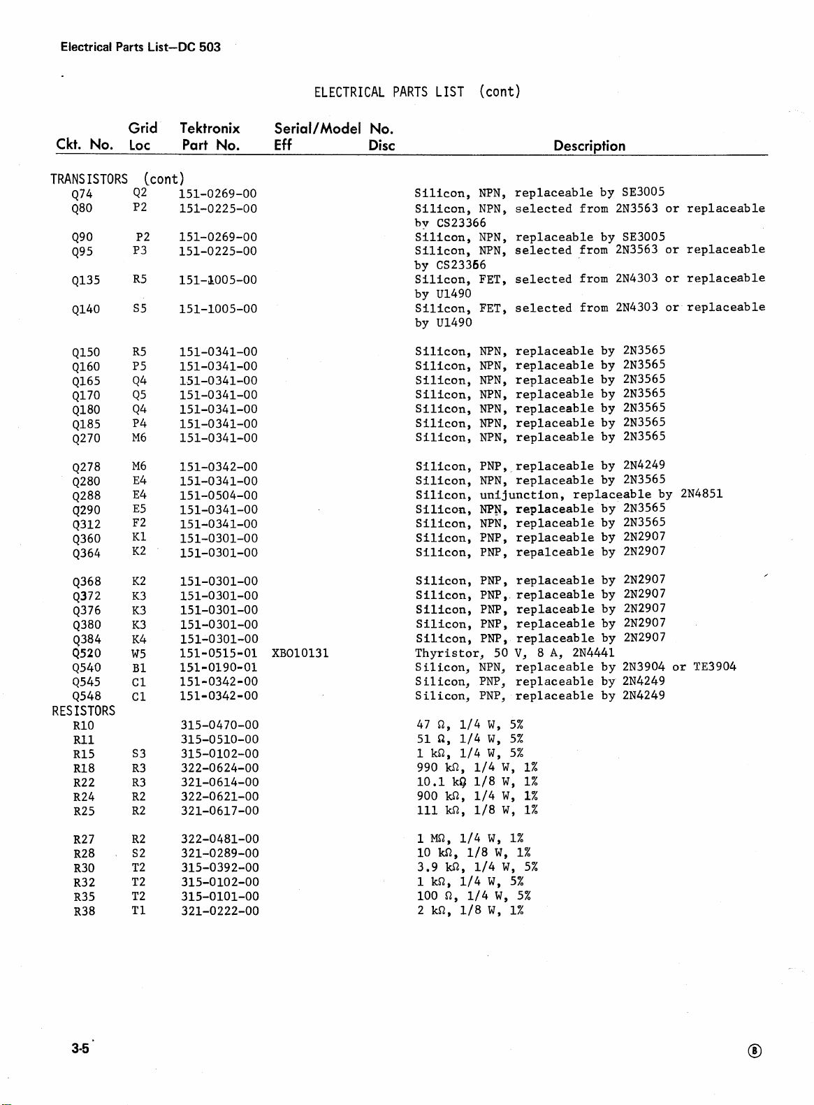
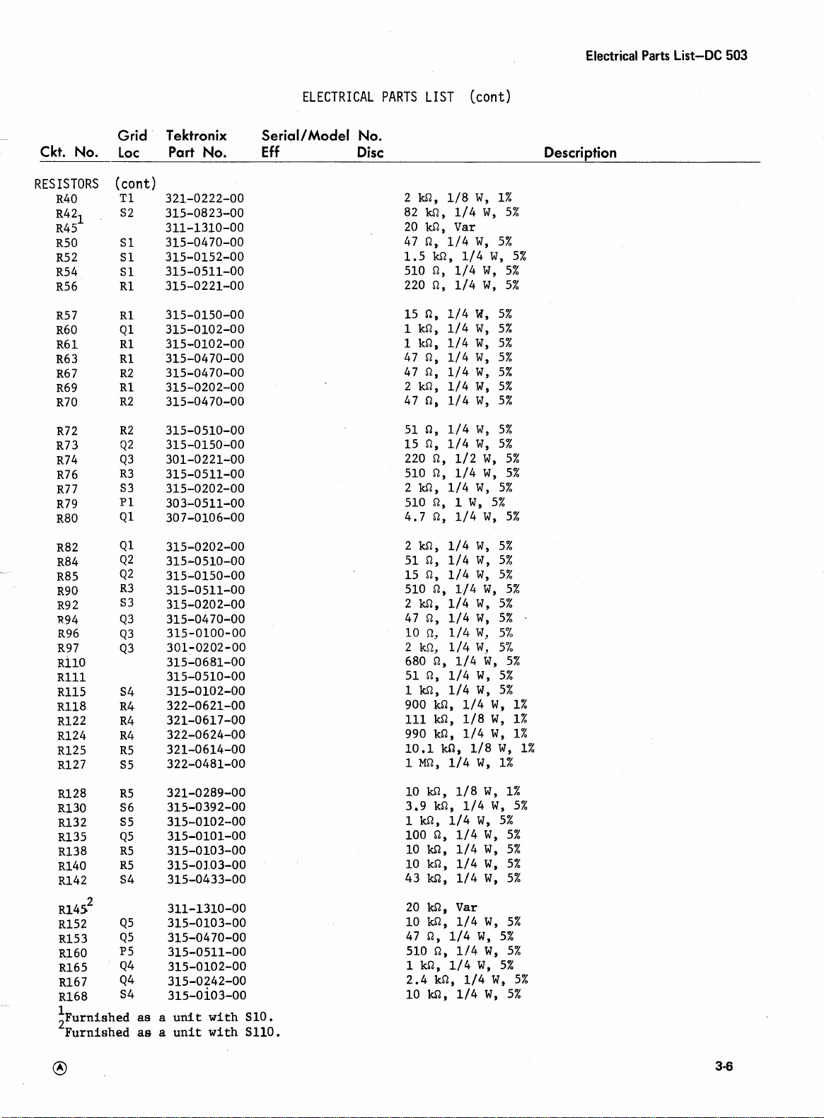
Replacement parts should be ordered from the Tektronix Field Office or Representative in your area.
Changes to Tektronix products give you the benefit of improved circuits and components. Please include
the instrument type number and serial number with each order for parts or service.
ABBREVIATIONS AND REFERENCE DESIGNATORS
Assembly, separable or F
repairable H
Attenuator, fixed or variable
Motor HR
Battery
Capacitor, fixed or variable
Ceramic
Diode, signal or rectifier
A!
cathode-ray tube M
R!T
Delay line
Indicating device ( lamp)
5;
Electrolytic P
electrolytic, metal cased PMC
electrolytic, metal tubular PT
Fuse
Filter
L
Heat dissipating device
(
heat sink, etc.
Heater
Connector, stationary portion
J
Relay
K
Inductor, fixed or variable
L
Inductor/resistor combination
L
R
Meter
Transistor or silicon-
Q
controlled rectifier
Connector, movable portion
Paper, metal cased
paper, tubular
.
)
LIST
paper or plastic, tubular
PTM
molded
Resistor, fixed or variable
Thermistor
Switch
Transformer
Test point
Assembly, inseparable or
non-repairable
Electron tube
Variable
Voltage regulator (zener diode,
etc.
1
wire-wound
Crystal
Tektronix Serial/Model No.
Part
No.
Eff
Disc
Description
DISPLAY Circuit Board Assembly
MAIN Circuit Board Assembly
MAIN
Circuit Board Assembly
TRIGGER
TRIGGER
AMP.
Circuit Board Assembly
AMP.
Circuit Board Assembly
PROTECTION Circuit Board Assembly
S3
T1
S1
R2
Q1
42
i5 Circuit . ~oard
68 pF, Cer, 500
uF, Cer, 500
0.01
170 pF, Cer, 500
0.01 pF, Cer, 150
0.1
uF,
Cer,
0.1 pF, Cer, 50
0.01
uF,
0.1 pF, Cer, 50
0.1 pF,
Cer,
24 pF, Cer, 500
pF, Cer, 50
0.1
0.1 pF, Cer, 50
0.1 pF, Cer, 50
0.1 pF, Cer, 50
0.01 pF, Cer, 500
--
V,
50
V
V
Cer, 150
V
50
V
V,
V
V
V
V
Assembly.
.
--
10%
V
V,
5%
V,
+80%-20%
V,
+80%-20%
5%
V
'standard only.
2~ption 1 only.
20
pF, Cer, 500
100 pF, Cer, 350
10
pF, Cer, 500
1000 pF, Cer, 500
pF, Cer, 150
0.01
0.1 pF, Cer, 50
0.1 pF, Cer, 50
0.1
uF,
Cer, 50
V,
V,
V,
V,
V,
V
V
V
10%
20%
10%
10%
+80%-20%
Page 22
Electrical Parts
List-DC
503
@rid Tektronix
Ckt. No.
boc Part
CAPACITORS
C138
C140
C141
C167
C170
C180
C187
No.
(cont)
R5 283-0003-00
S4 283-0111-00
R6 283-0111-00
P4
Q5 283-0111-00
44 283-0003-00
R3 283-0111-00
283-0003-00
ELECTRICAL PARTS LIST
SeriaVModel
Eff
No.
Disc
(cont)
.01 pF, Cer, 150
.1
pF, Cer, 50
.1
pF, Cer, 50
.O1
pF, Cer, 150
0.1
pF, Cer, 50
0.01 pF, Cer, 150
0.1 pF,
L
pF, Cer, 25
Cer,
10 pF, Cer, 500
pF, Cer, 500
18
1.9-15.7
1
pF, Elect., 35
10
pF, Elect., 25
510
33
pF, Elect., 10
0.001
pF, Var,
pF, Mica, 500
pF, Cer, 500
33 pF, Elect., 10
pF, Cer, 100
0.1
0.1 pF, Cer, 100
0.001 pF, Cer, 500
0.001 pF, Cer, 500
50
V
V
V
V
V,
V,
V,
+80%-20%
V,
+80%-20%
V,
980%-20%
V,
+80%-20%
10%
5%
Air,
V,
20%
V,
20%
V,
2%
V,
20%
V,
V,
20%
V,
+80%-20%
V,
+80%-20%
V,
V,
250
V
+loo%-0%
+loo%-0%
+fOO%-0%
DIODES
CK28
CR7
9
CR80
CB128
CRl79
CRl80
CU60
CR270
CR271
-\.
1
'standard only.
2~pcion 1 only.
0.001 pF, Cer, 500
0.001 pF,
Cer,
0.001 pF, Cer, 500
0.001
0.001 pF,
pF, Cer, 500
Cer,
0.001 pFy Cer, 500
47 pF, Elect., 20
100
pF,
Cer,
pP, Elect., 20
47
68
pFy
Elect., 6
pF, Cer, 200
650
100 pF, Cer, 350
100 pF,
Cer,
350
200
500
500
V,
V,
V,
V,
V,
V,
V,
V,
V,
V,
V,
V,
V,
+loo%-0%
+loo%-0%
9100%-0%
+loo%-0%
+loo%-0%
+loo%-0%
20%
5%
20%
20%
5%
20%
20%
4.7 pFy Elect., 50Vy 20%
0.001
15 pF, Elect., 50
6.8
pF,
Cer,
500
pF, Elect., 35
V,
V,
V,
20%
+loo%-OX
20%
Silic~n, replaceable by IN4152
Silicon, replaceable by IN4152
Silicon, replaceable by IN4152
Silicon, replaceable by IN4152
Silicon, replaceable by IN4152
Silicon, replaceable by IN4152
Silicon, replaceable by IN4152
SI~ICQB, replaceable by IN4152
Silicon, replaceable by IN4152
Page 23
Electrical Parts List-DC
503
Ckt.
No.
DIODES
CK290
ELECTRICAL PARTS LIST
Grid Tektronix SerialIModel
Loc
(~0;:)
Part
No.
Eff
XB010131 Zener, selected from 1N753A, 0,,4
(cont)
No.
Disc Description
Silicon,
Silicon, replaceable by IN4152
S ilicon, replaceable by IN4152
Silicon, replaceable by IN4152
Silicon,
Silicon,
Silicon,
Silicon,
Silicon,
Silicon,
Silicon, replaceable by IN4152
Silicon, replaceable by IN4152
Silicon, replaceable by IN4152
Silicon, replaceable by IN4152
Silicon, replaceable by IN4152
Silicon, replaceable by IN4252
Silicon, replaceable by IN4152
Zener, selected from 1N751AY 0.4
'Zener, selected from
replaceable by
replaceable by
replaceable by
replaceable by
replaceable by
replaceable by
replaceable by
IN4152
IN4152
IN4152
IN4152
IN4152
IN4152
IN4152
1N75lAY 0.4
W,
W,
W,
5.1
5.1
5.1
V,
V,
V,
5%
5%
5%
Lamp, LED, red
Numeric display, seven-segment, LED
Numeric display, seven-segment, LED
Numeric display, seven-segment, LED
Numeric display, seven-segment, LED
Numeric display, seven-segment, LED
Numeric display, seven-segment, LED
Numeric
Lamp, LED, red
Lamp, LED, red
Lamp, LED, red
display; seven-segment, LED
.
FUSE
F520 V5 159-0021-00 XB010131 Cartridge, 2A, 3AG, fast-blo
CONNECTORS
J10 131-0955-00 Receptacle, electrical,
JllO
5275 136-0491-00 Socket, banana jack
131-0955-00 Receptacle, electrical,
INDUCTORS
L18 R2
L523 N2
L549 02
Core, toroid ferrite
pH
2.7
5
c1H
TRANS ISTORS
435 T2
Silicon, FET, selected from 2N4392
Silicon, FET, selected from 2N4392
Silicon, NPN, selected From 2N3563 or replaceable
CS23366
by
Silicon, PNP, replaceable by 2N4258
Silicon, NPN, selected from 2N3563 or replaceable
CS23366
by
Silicon, NFN, selected from 2N3563 or replaceable
CS23366
by
BNC,
BNC,
female
female
Page 24
Electrical Parts List-DC
503
Ckt. No.
TRANS IS
TORS
474
480
ELECTRICAL PARTS LIST
Grid Tektronix SerialIModel No.
Loc Part No.
Eff
Disc Description
(cont)
42 151-0269-00
P2 151-0225-00
(cont)
Silicon, NPN, replaceable by
Silicon, NPN, selected from 2N3563 or replaceable
bv
CS23366
Silicon, NPN, replaceable by SE3005
Silicon, NPN, selected from 2N3563 or replaceable
CS23366
by
Silicon, FET, selected from 2N4303 or replaceable
U1490
by
Silicon, FET, selected from 2N4303 or replaceable
U1490
by
Silicon, NPN, replaceable by 2N3565
Silicon,
Silicon, NPN, replaceable by 2N3565
Silicon, NPN, replaceable by 2N3565
Silicon, NPN, replaceable by 2N3565
Silicon, NPN, replaceable by 2N3565
Silicon, NPN, replaceable by 2N3565
Silicon, PNP, replaceable by 2N4249
Silicon, NPN, replaceable by 2N3565
Silicon, unijunction, replaceable by 2N4851
Silicon,
Silicon, NPN, replaceable by 2N3565
Silicon, PNP, replaceable by 2N2907
Silicon, PNP, repalceable by 2N2907
NPN,
replaceable by 2N3565
NPN,
replaceable by 2N3565
SE3005
4368
4372
4376
Q380
Q384
Q520
4540
4545
4548
RESISTORS
R10
R11
R15
R18
R2 2
R24
R25
Silicon, PNP, replaceable by 2N2907
Silicon, PNP, replaceable by 2~2907
Silicon, PNP, replaceable by 2N2907
Silicon, PNP, replaceable by 2N2907
Silicon, PNP, replaceable by 2N2907
Thyristor, 50
Silicon, NPN, replaceable by 2N3904 or TE3904
Silicon, PNP, replaceable by 2N4249
Silicon, PNP, replaceable by 2N4249
1
MC2,
114
10
M,
118
3.9
Wz,
1
kQ, 114
Q,
100
2
114
kQ, 118
1/4
W,
W,
W,
W,
W,
W,
V, 8 A,
1%
1%
5%
5%
5%
1%
2N4441
Page 25
Electrical Parts List-DC
503
-
Ckt. No.
RESISTORS
R40
R4
R45
R50
R52
R54
R56
z1
ELECTRICAL PARTS LIST
Grid Tektronix Serial/Model No.
Loc Part No.
(cont)
TI 321-0222-00
S2 315-0823-00
311-1310-00
S1 315-0470-00
S1 315-0152-00
S1 315-0511-00
R1 315-0221-00
Eff
Disc Description
2
W2,
82
20
47
1.5
510
220
118
W2,
114
kQ,
Var
Q,
114
kS2,
Q,
114
n,
114
(cont)
W,
W,
W,
114
W,
W,
w,
1%
5%
5%
5%
5%
5%
R82
\
R84
R85
R90
R9 2
R94
R96
R97
RllO
Rlll
R115
R118
R122
R124
R125
R127
i~urnished
Furnished
as
as
a
a
unit with
unit with
S10.
S110.
20
10
47
510
1
kQ,
2.4
10
W2,
W2,
Q,
a,
k0,
W2,
Var
114
114
1/4
114
114
114
W,
W,
W,
W,
W,
W,
5%
5%
5%
5%
5%
5%
Page 26

Electrical Parts List-DC
503
ELECTRICAL PARTS LIST (cont)
Ckt. No.
RESISTORS (cont)
R172
Q6
R174 R5
R179 P5
R180
Q4
R182 S4
R187 05
Tektronix
Bart
No.
SerialIModel No.
Eff
BOlOlOO
Disc
B049999 le5kQ,1/4W,5%
B050000 300
BOlOlOO
B050000
B049999 3.3
1
300
1
5.6
270.0, 114
180
W,
kQ,
fl,
kQ,
114
0,
114
kQ,
0,
114
114
114
114
114
W,
W,
W,
W,
W,
W,
W,
5%
5%
W,
Description
5%
5%
5%
5%
5%
5%
'standard only.
'~urnished
as
a unit with
S285.
2
kQ,
510
5.6
5.1
1
WZ,
500
10
1
kQ,
510
510
5.6
5.6
1
WT,
2.4
1
kC2,
2.4
1
m,
1
WZ,
5.6
2.4
1
kQ,
n,
kQ,
kQ,
kS1,
Q,
Q,
0,
kQ,
kQ,
kQ,
kQ,
kQ,
kC2,
114
114
1/4
114
114
Var
114
114
1/4
114
114
114
114
114
114
114
114
114
114
114
114
W,
w,
W,
W,
W,
W,
W,
W,
W,
W,
W,
W,
5%
W,
W,
5%
5%
5%
W,
W,
5%
W,
5%
W,
5%
5%
W,
W,
5%
5%
5%
5%
5%
5%
5%
5%
5%
5%
5%
5%
Page 27

Electrical Parts List-DC
503
-,
Cke. No.
Grid
LOC
Tektronix
Part No.
ELECTRICAL PARTS
SerialIModel No.
Eff
Disc
LIST
(cont)
300
n,
114
W,
5%
5.6
Q,
114
W,
5%
3.3
kS2,
114
W,
5%
1
kn,
Var
3
kS2,
114
W,
5%
1.5
kR,
114
W,
5X
56
BOlOlOO B079999 56
B080000 180
XB010131
d
'standard only.
n,
1
kS2,
0.3
1.6
4.99
2.49
20
kQ,
5.1
22.1
2.7
2.7
2.7
15.8
n, 2 W,
Q,
kn,
kS2,
kn,
kn,
kn,
kn,
W,
0,
kn,
n, 2 w,
2
W,
114
3
114
1/4
1/4
114
114
112
5x
5%
W,
W,
118
118
W,
118
W,
118
10%
5%
WW,
W,
W,
W,
5%
W,
W,
W,
W,
5%
W,
1%
5%
1%
1%
5%
1%
5%
5%
1%
'option 1 only.
Page 28

Electrical Parts List-DC
503
ELECTRICAL PARTS LIST (cont)
Ckt Grid
No.
INTEGRATED CIRCUITS
U1
U212 02
U214 01 156-0100-00
l~urnished as a unit with R45.
2~urnished as a unit with R145.
3~urnished as a unit with R285.
4
5Standard only.
Loc
Option
1
only.
Tektronix
Part No.
156-0118-00 XB060000
.
156-0100-00
Serial/Model No.
Eff
BOlOlOO
BOlOlOO
Disc
B059999X Single 40
B059999X Single 40
(INT SOURCE PULL)
Push, ATTENUATOR
AC,
Push'
Push, ATTENUATOR
Push,
Actuator assembly,
Actuator assembly, FUNCTION
Push,
HOLD, DISPLAY TIME
Dual 100
replaceable by
Quad 2-input nand gate, replaceable by SN74500N
Quad 2-input nand gate, replaceable by SN74500N
Dual 100
replaceable by
+
SLOPE (Out
AC,
DC
+
SLOPE (Out
RESET
START
(OUTcSTOP)
MHz
MHz
Coupling
J-K
J-K
MHz
replaceable by
MHz
replaceable by
Quad 2-input positive nand gate, replaceable
SN7400N
by
Dual 15
replaceable
Triple 3-input positive nand gate, replaceable
by
Quad 2-input positive nand gate, replaceable
by
Single 10
replaceable by
Single 10
replaceable by
Single 10
replaceable by
Single 10
replaceable by
Single 10
replaceable by
Single 10
replaceable by
Single 10
replaceable by
Single 10
replaceable by
MHz
SN7410N
SN7400N
D-type pos-edge-trig flip-flop
by
MHz
MHz
MHz
MHz
MHz
MHz
MHz
MHz
CHA
XlOO
CHA
x10
DC
Coupling
-)
XI0
CHB
xlOO
-)
N/CLOCK
mas ter-s lave flip-flop,
SN74S112
master-slave flip-flop,
SN74S112
J-K
edge-triggered flip-flop,
SN74H102
J-K
edge-triggered flip-flop,
SN74H102
RATE
,
SN7474N
divide-by-2-&-5 ripple counter,
SN7490N
divide-by-2-&-5 ripple counter,
SN7490N
divide-by-2-&-5 ripple counter,
SN7490N
divide-by-2-&-5 ripple counter,
SN7490N
divide-by-2-&-5 ripple counter,
SN7490N
divide-by-2-&-5 ripple counter,
SN7490N
divide-by-2-&-5 ripple counter,
SN7490N
divide-by-2-&-5 ripple counter,
SN7490N
-
Page 29

ELECTRICAL PARTS LIST (cont)
Electrical Parts List-DC
503
Ckt
No.
INTEGRATED CIRCUITS ( cont
U270 F3 156-0042-00
Grid
Tektronix
Loc Part No.
SerialIModel No.
Eff
)
BOlOlOO
B050000 Dual 15
BOlOlOO
B050000 Dual 15
Disc
Dual 15
replaceable by
20
Dual
replaceable by
Quad 2-input positive nand buffer, replaceable
by
SN7473N
Single 10
replaceable by
Single 10
replaceable by
Single 10
replaceable by
Single 10
replaceable by
Single 10
replaceable by
Single 10
replaceable by
Dual 15
by
SN7473N
Quad latch, replaceable by MC4035P
Quad latch, replaceable by MC4035P
Quad latch
Quad latch, replaceable by MC4035P
Quad latch, replaceable by MC4035P
Quad latch, replaceable by MC4035P
Quad latch , replaceable by MC40 35P
Quad 2-input positive nand gate, replaceable
SN7401N
by
Quad 2-input positive nand gate, replaceable
SN7401N
by
B049999 Dual 15
replaceable by
replaceable by
B049999 Dual 15
replaceable by
replaceable by
Single BCD-to-decimal decoderldriver, replaceable
by
SN74145N
Hex. inverter, replaceable by SN7404N
Single BCD-to-seven segment decoderldriver,
replaceable by SN7447N
Dual 4-input positive nor gate, replaceable by
SN7425N
Quad 2-input positive nor gate, replaceable by
SN7425N
Quad 2-input positive nor gate, replaceable by
SN7425N
Voltage regulator, replaceable by UA723C
Voltage regulator, replaceable by UA723C
Description
MHz
J-K
mas ter-slave flip-flop,
MHz
MHz
SN7476N
J-K
master-slave flip-flop,
SN74111N
MHz
divide-by-2-&-5 ripple counter,
SN7490N
MHz
divide-by-2-&-5 ripple counter,
SN7490N
MHz
divide-by-2-&-5 ripple counter,
SN7490N
MHz
divide-by-2-&-5 ripple counter,
SN7490N
MHz
divide-by-2-&-5 ripple counter,
SN7490N
MHz
divide-by-2-&-5 ripple counter,
SN7490N
J-K
master-slave flip-flop, replaceable
replaceable by MC4035P
,
.
MHz
D-type pos-edge-trig flip-flop,
SN7474N
MHA
D-type pos-edge-trig flip-flop,
SN7474N
MHz
D-type pos-edge-trig flip-flop,
SN7474N
MHz
D-type pos-edge-trig flip-flop,
SN7474N
CRYSTALl
Y2502 C5 158-00 79-00
P251 C5 119-0262-00
:standard only.
Option
1
only.
Crystal,
Oscillator,
1'
MHz
RF
+0.001%
Page 30

INTERNAL ADJUSTMENTS PROCEDURE
Services Available
I
Tektronix,
adjustment at local Field Service Centers and at the Factory
Service Center. Contact your local TEKTRON
Office or representative for further information.
Test
Equipment
For measurement of the power supply voltages,
ohmslvolt
example, Triplett 630 NA multimeter.
A
lox
time base reference to the oscilloscope to prevent excessive
loading.
For
,
frequency standard or other frequency source having
stability of
measuring optional 5 MHz crystal output) is recommended
nc. provides complete instrument repair and
VOM
will give satisfactory measurements. For
probe is required to connect the DC 503 I-MHz
1
-MHz frequency measurement,
at
least 5 parts on
lo7
a
secondary Power Supply Checks and Adjustment. Connect the
(5 parts in
lX Field
a
20,000
a
lo8
if
for accuracy. Also recommended is a test oscilloscope with
at
a bandwidth of
for frequency-comparison measurement.
least 1 MHz and a stable triggering circuit
Procedure
NOTE
The performance of this instrument can be check at
0°C
to
any temperature within the
Make any adjustment at a temperature between
+20"~
TM
extender (TEKTRGN
voltmeter between the +15-volt test point and ground.
Adjust R505 for
+5 volt and -22-volt supplies to be within 5%.
and
+30"~ (+68"
The DC 503 can be operated either fully installed in a
500 Series Power Module
a
reading of +15-volts. Then check the
F
and
or
IX Part No. 067-0645-01).
+50°c
+86"
F).
connected
to
range.
a
plug-in
NOTE
If
the instrument is operated on the plug-in extender,
the +5-volt supply may not regulate.
Secondary
standard
Time-Base Frequency Check and Adjustment. Connect
the
DC
503 1-MHz time base reference and the secondary
standard to the oscilloscope as shown. Adjust the oscilloscope to display several complete cycles.
0
1
1
MHz
l nput
O
Ext
Trig
NOTE
I;
1
MHz
Option
removing the slotted plug from the crystal oven to
gain access to interior adjusting slug.
To determine oscillator error, observe the rate of
horizontal drift of the displayed waveform. Waveform
moving to the right indicates that the time-base frequency
is
<I
MHz; to the left, > 1 MHz. The period in seconds for
the waveform to move the width of one cycle is equal to
the frequency difference in parts in
the waveform drifts to the right at a rate of one cycle's
width every 10 seconds, the time-base frequency
in
lo6
low. Maximum allowable frequency difference
part in
Adjust C255 for no drift.
lo5
(5 parts in
clock adjustment is made
lo6.
For example, if
lo7
for the optional 5 MHz crystal).
is
0.1 part
by
is
1
+5 V Test Point
R522
+I5 V Adjust
R505
+I5 V Test Point
R502
v
-22
Test Point
R542
/
Outline indicates area occupied by crystal oven
when option 1 is installed. Components inside
outline are removed when option is installed.
1
MHz
I
Clock
C255
1
MHz
Test Point
U272,
Pin 5
@
Page 31

FRONT
Attenuation Pushbuttons
Two self-canceling buttons
select XI,
attenuation of the input
signal.
LEVEL Control
Selects the amplitude point
on the input
signal input source. Pulled
out selects the rear connector input. Pushed in
the front-panel BNC connector input.
X10,
\ \
signal at
selects
PANEL
or XlOO
CONTROLS & CONNECTORS
Display Readout
LED readout, seven
segment
matically placed decimal
point. The leading zeroes
are
overflow is indicate1
d~g~ts with auto-
~~DDresSed unless an
..
L
7-
Units Indicators
LED indicates that
played number is MHz
(106), or kHz (103) if in
CDCn
A
--_I--
(100) if in a time mode. In
the RATIO
TOTALIZE A modes, no
units are indicated.
AIB and
/
FUNCTION Switch
Selects measurement or
time counting modes for
counter. Also selects the
gate (measurement) interval in the four FREQ A
positions.
Gate Indicator
Lights
/
during the active
gating
interval.
dis-
-
Manual Gate Pushbutton
Push-push switch operable
TlME MANUAL or
when
Gate Output Connector
Provides a
inciding with the measurement interval.
INPUT Connector
BNC connector for signal
input.
Input Coupling Pushbutton
A push-push switch which
selects whether the input Variable control concentric
signal is AC or DC coupled with
into the attenuators. switch sets the
Trigger
A push-push switch which
selects the slope of the
input signal on which triggering will occur.
+5-volt pulse co-
Slope Pushbutton
/
/
Selects the gate (measure-
ment) interval for the
RATIO
TlME A--PB and TlME
MANUAL modes of the
FUNCTION switch.
AIB, PERIOD
6,
:\,
:
which manually resets (acts
as a master reset) and
vides a segment check of
the
I
Ground Connector
Provides a chassis return
for signals.
TOTALIZE A is selected
by the FUNCTION switch.
Button in starts the
u re men
button out terminates the
gate.
RESET Pushbutton
Monentary
7
readout digits.
.
t
pushbunon
DISPLAY
NICLOCK RATE
+;ma
+he
.llllr
displayed after the count is
made and before the next
measurement is taken. Display time can be varied
from 0.1 s
10 seconds
position
continuous display until reset by pressing the RESET
button.
i
nterval gate;
pro-
TIME Control
~a-rl;.-.~
I=aUltlg
(ccw) to about
(cw). HOLD
(detent) provides
meas-
'--m+'-
lelmyttm
will be
-*
Page 32
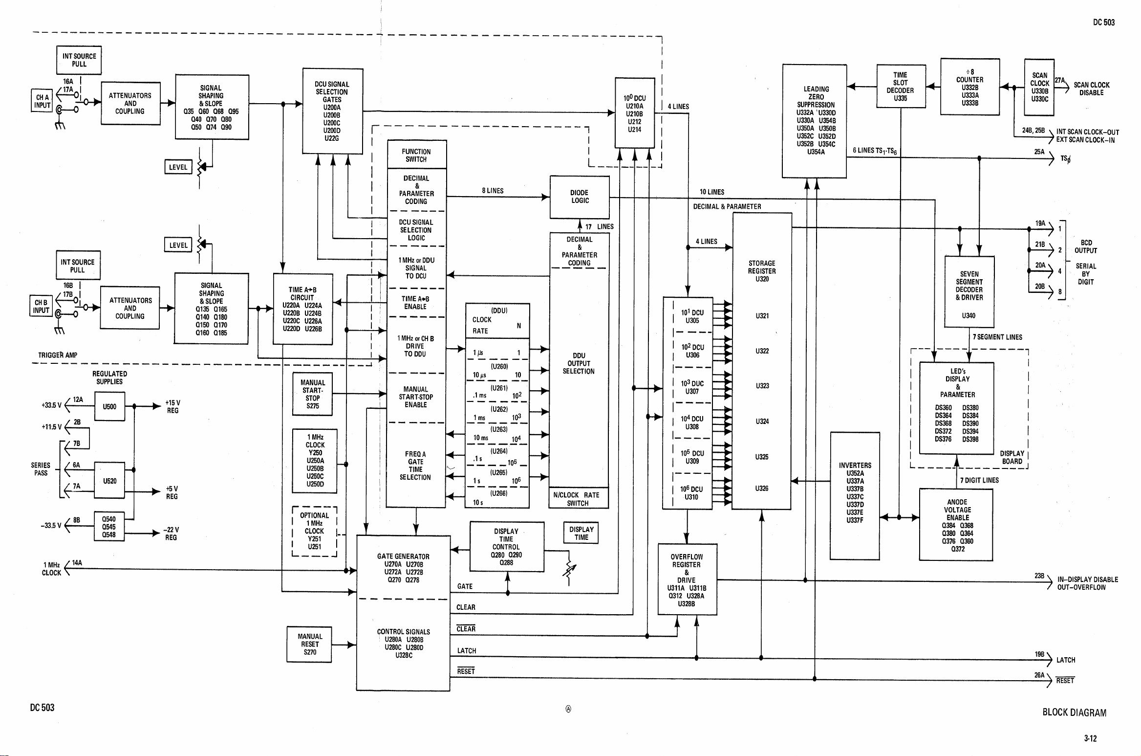
MANUAL
RESET
CONTROL SIGNALS
U280A U280B
U280C U280D
U328C
-
CLEAR
LATCH
-
RESET
A
A
w
A
-
1
19B
LATCH
f
8
BLOCK
DIAGRAM
Page 33
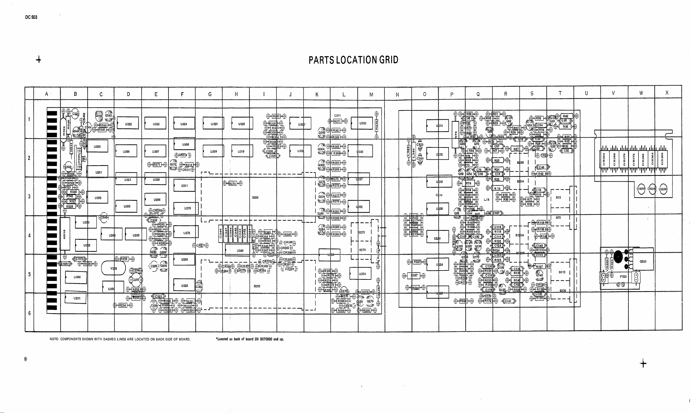
PARTS LOCATION GRID
NOTE: COMPONENTS SHOWN WITH DASHED LINES ARE LOCATED ON BACK SIDE OF BOARD.
*Located
on
back
of
board
SN
8070000
and
up.
Page 34
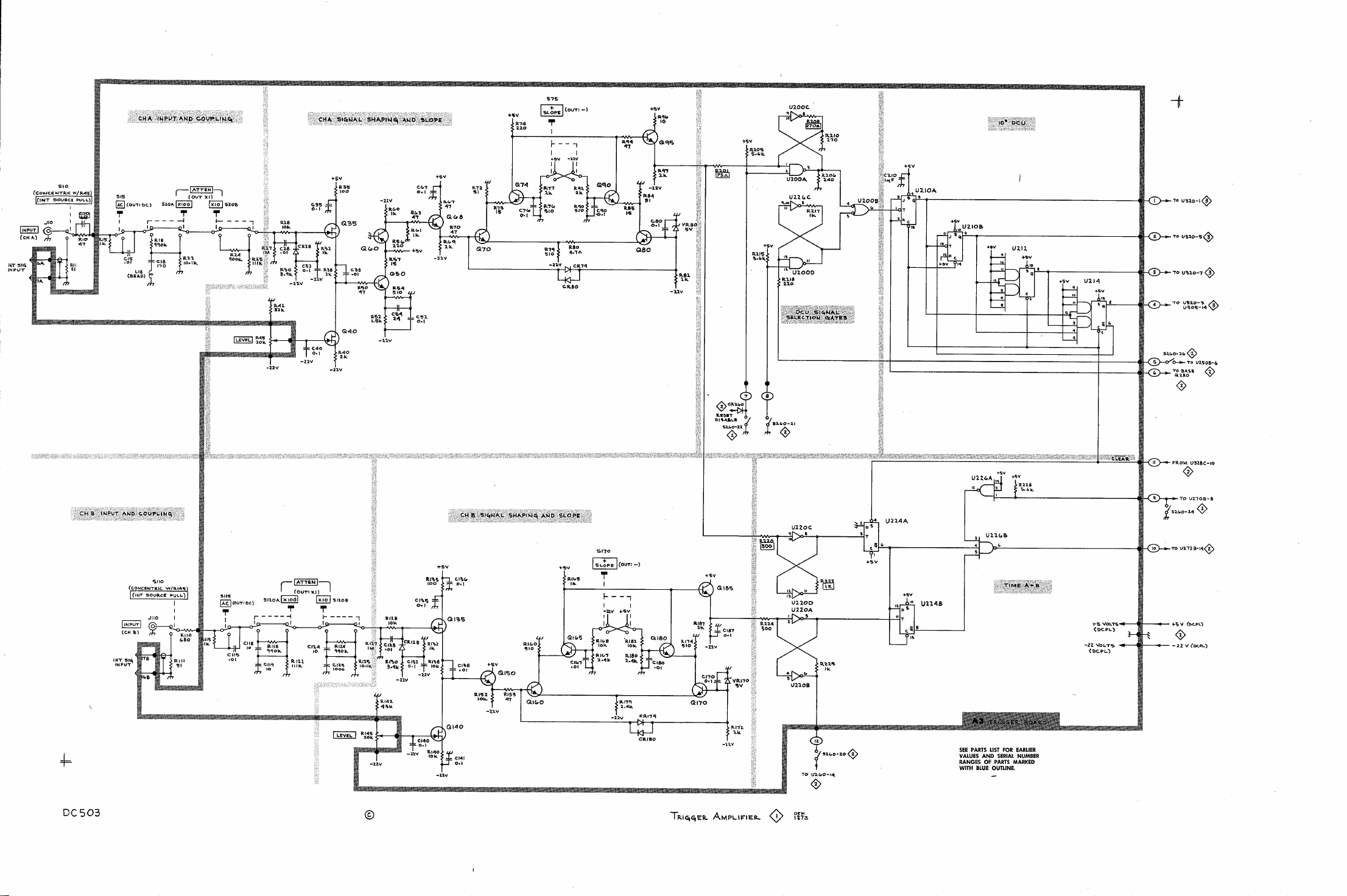
IUT
IN
P
5170
SEE PARTS LIST FOR EARLIER
VALUES AND SERIAL NUMBER
RANGES OF PARTS MARKED
WITH
BLUE OUTLINE.
-
Page 35
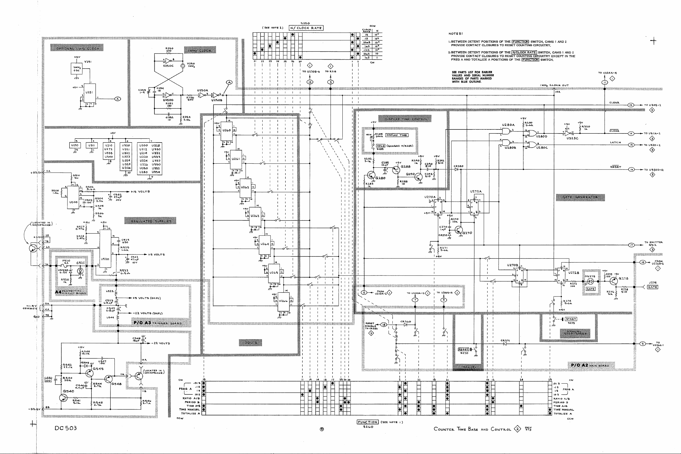
Page 36
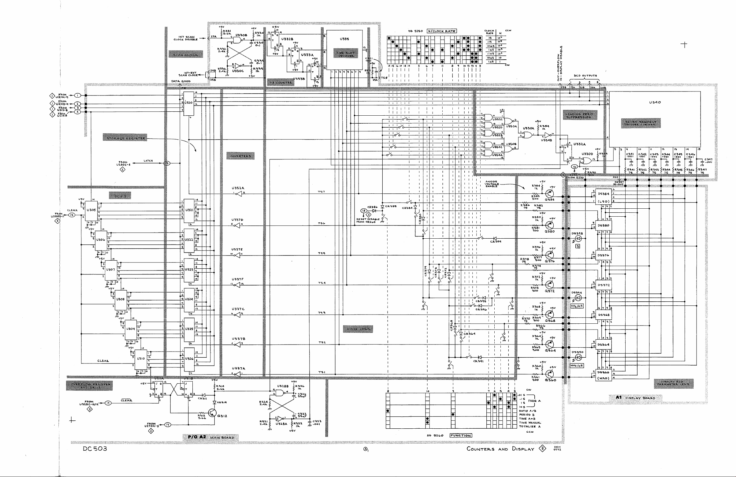
Page 37
Replacement parts should be ordered from the Tektronix Field Office or Representative in your area.
Changes to Tektronix products give you the benefit of improved circuits and components. Please include
the instrument type number and serial number with each order for parts or service.
ABBREVIATIONS
binding head brass
binding head steel
cathode-ray tube
countersunk
double end
flat head brass
flat head steel
fillister head brass
fillister head steel
Fig.
BHB
BHS
CRT
csk
DE
FHB
FHS
Fil HB
Fil HS
&
lndex Tektronix SerialIModel No.
No. Part No.
ff
.
Disc
h
hex.
HHB
HHS
HSB
HSS
ID
lg
OD
height or high
hexagonal
hex head brass
hex head steel
hex socket brass
hex socket steel
inside diameter
length or long
outside diameter
t
Y
1234s
OHB
OHS
PHB
PHs
RHS
SE
THB
THS
W
Description
oval head brass
oval head steel
pan head brass
pan head steel
round head steel
single end
truss head brass
truss head steel
wide or width
337-1399-00
BOlOlOO
337-'1399-00 B050000
337-1399-02 B050000
366-0494-00
------
213-0153-00
366-1190-00
------
2.13-0153-00
366-1031-05
------
2l3-0153-00
366-1170-01
------
2l3-0153-00
366-1422-00
366-1422-01 B010152
214-1840-00 XB010152
366-1257-87
366-1402-41
366-1257-27
366-1257-28
366-1402-64
366-1257-30
3'58-0029-00
-
- - -
2:LO-0590-00
2:LO-09 78-00
BOlOlOO
- -
B049999
B010151
SHIELD, electrical, side
SHIELD, electrical, side
SHIELD, electrical, side
KNOB,
gray--LEVEL (CHA & CHB)
each knob includes:
SETSCREW, 5-40 x 0.125 inch, HSS
KNOB,
gray--FUNCTION
knob includes
:
SETSCREW, 5-40 x 0.125 inch, HSS
KNOB
red--DISPLAY TIME
knob includes
:
SETSCREW, 5-40 x 0.125 inch, HSS
KNOB,
gray--CLOCK RATE
knob includes
:
SETSCREW, 5-40 x 0.125 inch, HSS
KNOB,
KNOB,
latch
latch
PIN, knob, latch
PUSHBUTTON--XI0
PUSHBUTTON--XI00
PUSHBUTTON--AC COUPL
PUSHBUTTON--+ SLOPE
PUSHBUTTON--IN START OUT STOP
PUSHBUTTON--RESET
BUSHING, 0.375-32 x 0.50 inch
mounting hardware for each
NUT, hex., 0.375-32
WASHER, flat, 0.375
x
ID
:
0.438 inch
x
0.50 inch
(not included wlbushing)
OD
NUT, knurled, 0.25-28 x 0.375 inch
OD
STUD, binding post
SOCKET, banana jack
mounting hardware: (not included
NUT, hex., 0.25-32
x
0.312 inch
wlsocket)
LUG, terminal, SE
WASHER, insulating, 0.375 inch diameter
Page 38
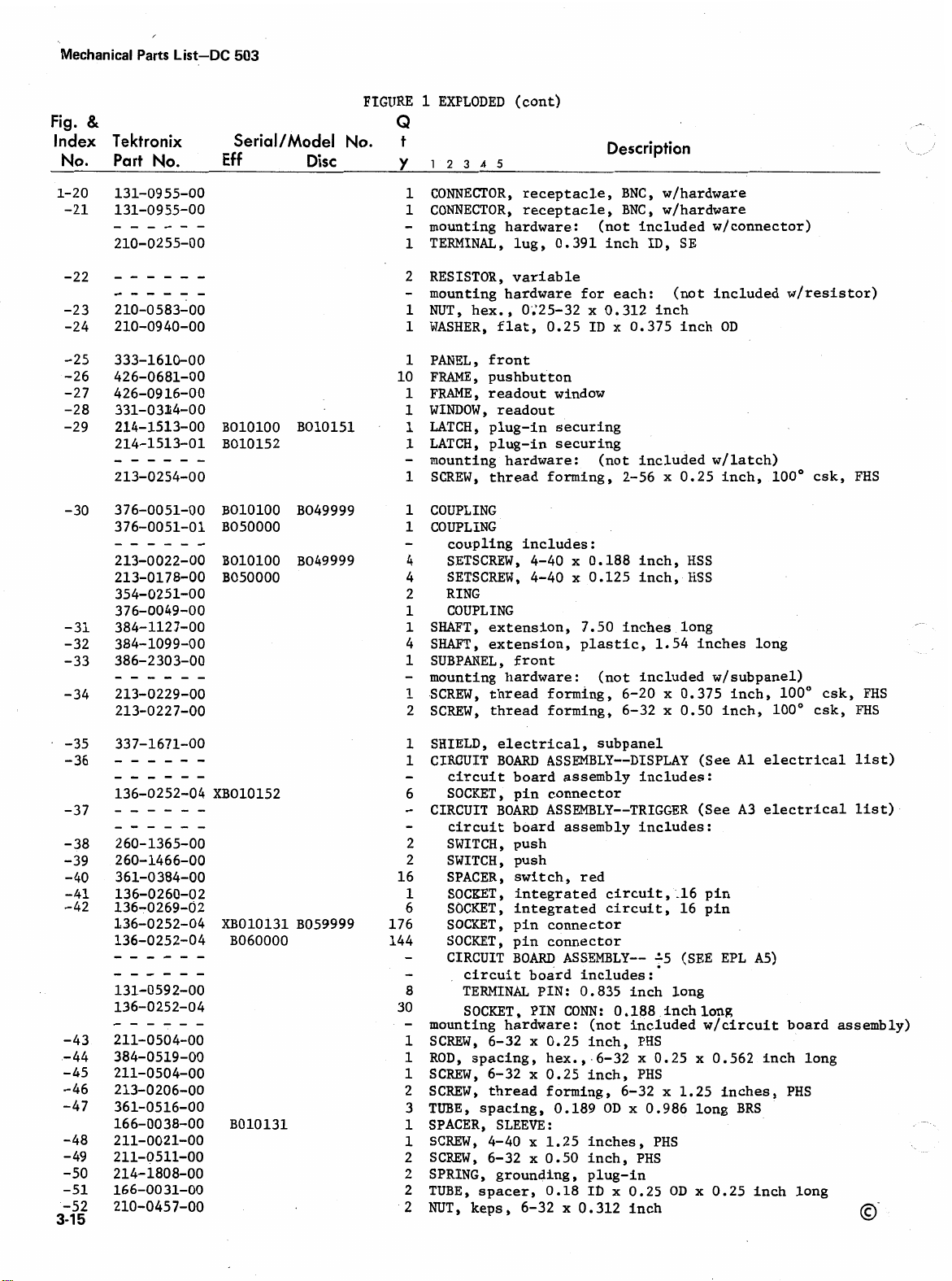
Mechanical Parts List-DC
Fig.
&
503
FIGURE 1 EXPLODED (cont)
Index Tektronix SerialIModel No. t
No. Part
No.
Eff
Disc
Q
y
12345
1
CONNECTOR, receptacle,
1
CONNECTOR, receptacle,
-
mounting hardware: (not included w/connector)
1
TERMINAL, lug, 0.391 inch
2 RESISTOR, variable
-
mounting hardware for each: (not included wlresistor)
1
NUT, hex., O'i25-32 x 0.312 inch
1
WASHER, flat, 0.25
Description
BNC,
BNC,
ID,
ID
x 0.375 inch
wlhardware
wlhardware
SE
OD
333-1610-00
426-0681-00
426-0916-00
331-0314-00
214-1513-00
214-1513-01 B010152
BOlOlOO
------
213-0254-00
376-0051-00
376-0051-01 B050000
BOlOlOO
------
213-0022-00
213-0178-00 B050000
354-0251-00
376-0049-00
384-1127-00
384-1099-00
386-2303-00
BOlOlOO
B010151
B049999
B049999
PANEL, front
FRAME, pushbutton
FRAME, readout window
WINDOW, readout
LATCH, plug-in securing
LATCH, plug-in securing
mounting hardware: (not included
SCREW, thread forming, 2-56 x 0.25 inch, 100" csk, FHS
COUPLING
COUPLING
coupling includes:
SETSCREW, 4-40 x 0.188 inch, HSS
SETSCREW, 4-40 x 0.125 inch, HSS
RING
COUPLING
SHAFT, extension, 7.50 inches long
SHAFT, extension, plastic, 1.54 inches long
SUBPANEL, front
mounting hardware
SCREW, thread forming, 6-20 x 0.375 inch, 100" csk, FHS
SCREW, thread forming,
SHIELD, electrical, subpanel
CIRCUIT BOARD ASSEMBLY--DISPLAY (See
circuit board assembly includes:
SOCKET, pin connector
CIRCUIT
circuit board assembly includes
SWITCH, push
SWITCH, push
SPACER, switch, red
SOCKET, integrated circuit,-16 pin
SOCKET, integrated circuit, 16 pin
SOCKET, pin connector
SOCKET, pin connector
-
CIRCUIT BOARD ASSEMBLY-- f5 (SEE EPL A5)
-
mounting hardware: (not included wlcircuit board assembly)
SCREW,
ROD,
SCREW,
SCREW, thread forming,
TUBE, spacing, 0.189
SPACER, SLEEVE
1
SCREW, 4-40 x 1.25 inches, PHs
2 SCREW, 6-32 x 0.50 inch, PHs
2 SPRING, grounding, plug-in
2
TUBE,
2 NUT, keps, 6-32
BOARD
circuit board includes
TERMINAL PIN: 0.835 inch long
SOCKET, PIN
6-32 x 0.25 inch,
spacing, hex., - 6-32 x 0.25 x 0.562 inch long
6-32 x 0.25 inch,
spacer, 0.18
ASSEMBLY--TRIGGER (See A3 electrical list)
:
(not included
:
CONN:
x
0.188 inchlong
OD
ID
x
0.312 inch
6-32 x 0.50 inch, 100° csk,
:
PHs
PHs
6-32 x 1.25 inches,
x 0.986 long BRS
0.25
wllatch)
w/
subpanel)
A1
electrical list)
:
OD
x 0.25 inch long
PHs
FHS
@-
Page 39
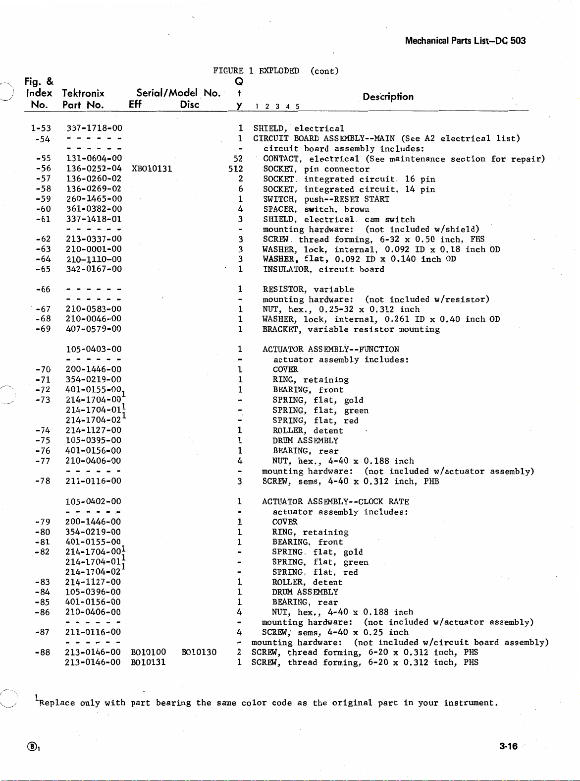
Mechanical Parts List-DC
FIGURE 1 EXPLODED (cont)
-
Fig.
&
Q
SHIELD, electrical
CIRCUIT BOARD ASSEMBLY--MAIN (See A2 electrical list)
circuit board assembly includes:
CONTACT,
SOCKET, pin connector
SOCKET. integrated circuit. 16 pin
SOCKET, integrated circuit, 14 pin
SWITCH, push--RESET START
SPACER, switch, brown
SHIELD, electrical. cam switch
mounting hardware: (not included
SCREW. thread forming, 6-32 x 0.50 inch, FHS
WASHER, lock, internal, 0.092
WASHER, flat , 0.092
INSULATOR, circuit board
1
RESISTOR, variable
-
mounting hardware: (not included w/resistor)
1
NUT, hex., 0.25-32 x 0.312 inch
1
WASHER, lock, internal, 0.261
1
BRACKET, variable resistor mounting
electrical (See maintenance section for repair)
wlshield)
ID
ID x 0.140 inch
x 0.18 inch
OD
ID
x 0.40 inch
503
OD
OD
ACTUATOR ASSEMBLY--FUNCTION
actuator assembly includes:
COVER
RING,
BEARING, front
SPRING, flat, gold
SPRING, flat, green
SPRING, flat, red
ROLLER, detent
DRUM
BEARING, rear
NUT, hex., 4-40 x 0.188 inch
mounting hardware: (not included
SCREW, sems, 4-40
ACTUATOR ASSEMBLY--CLOCK RATE
actuator assembly includes:
COVER
RING,
BEARING, front
SPRING. flat, gold
SPRING, flat, green
SPRING, flat, red
ROLLER, d e
DRUM
BEARING, rear
NUT, hex,, 4-40
mounting hardware: (not included
SCREW; sems, 4-40 x 0.25 inch
mounting hardware: (not included
SCREW,
SCREW,
retaining
.
ASSEMBLY
x
0.312 inch, PHB
retaining
t
en
ASSEMBLY
thread forming, 6-20 x 0.312 inch,
thread forming, 6-20 x 0.312 inch,
t
x
0.188 inch
w/actuator assembly)
wlactuator assembly)
w/circuit board assembly)
PHs
PHs
//
J
l~e~lace only with part bearing the same color code as the original part in your instrument.
Page 40
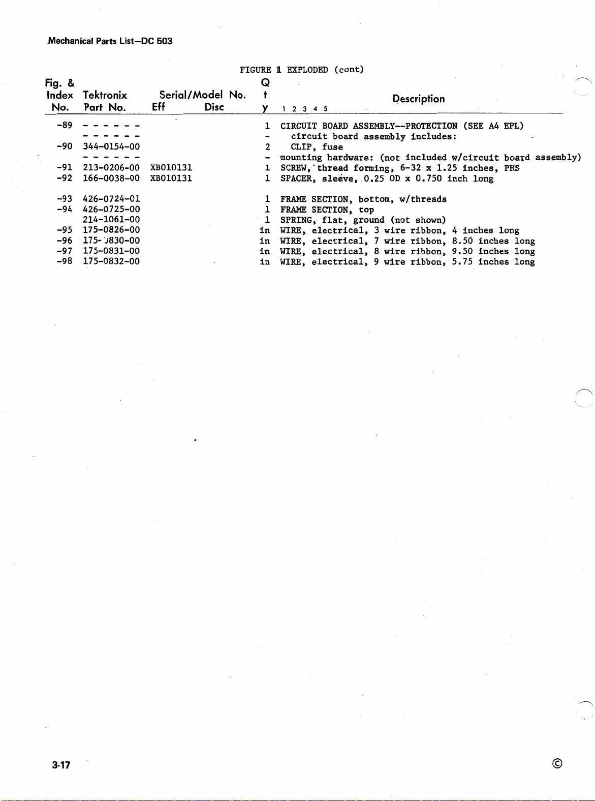
Mechanical Parts List-DC
Fig.
&
Index Tektronix SerialIModel No.
No. Part No.
503
Eff
Disc
FIGURE 1 EXPLODED (cont)
Q
t
y
12345
/--,
Description
CIRCUIT BOARD ASSEMBLY--PROTECTION
(SEE
A4
EPL)
circuit board assembly includes:
CLIP, fuse
mounting hardware
:
(not included wlcircuit board assembly)
SCREW,'thread forming, 6-32 x 1.25 inches, PHs
SPACER, sleeve,
FRAME
FRAME
SECTION, bottom, wlthreads
SECTION, top
0.25
OD
x
0.750
inch long
SPRING, flat, ground (not shown)
4
WIRE, electrical, 3 wire ribbon,
WIRE, electrical,
WIRE, electrical,
WIRE, electrical,
7
wire ribbon,
8
wire ribbon,
9
wire ribbon,
inches long
8.50
inches long
9.50
inches long
5.75
inches long
Page 41
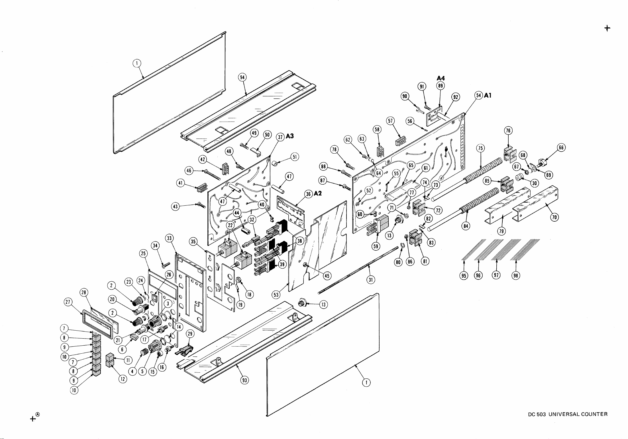
DC
503
UNIVERSAL
COUNTER
Page 42

ACCESSORI ES
Fig.
&
Index Tektronix SerialIModel No.
No. Part No.
Eff
Disc
Q
t
y
1 2 3 4 5 Description
REPACKAGING
2-
070-141 1-00 1
MANUAL, instruction
DC
503
UNIVERSAL COUNTER
Fig.
&
lndex
No.
Tektronix
Part No.
SerialIModel No.
Eff
Disc
Q
t
y
12345 Description
CARTON ASSEMBLY
carton assembly includes:
FRAME
END CAP, front
END CAP, rear
PAD
CARTON
Page 43

Page 44

DC
503
EFF
SN E060000-up
Page
1
of
2
I"--
\-/
REMOVE
ELECTRICAL PARTS
:
LIST
AND SCHEWTIC CORRECTION
Single 40
MHz
replaceable by
J-K
edge-triggered flip-flop,
SN74H102
Page 45

Page 46

Page 47

Page 48
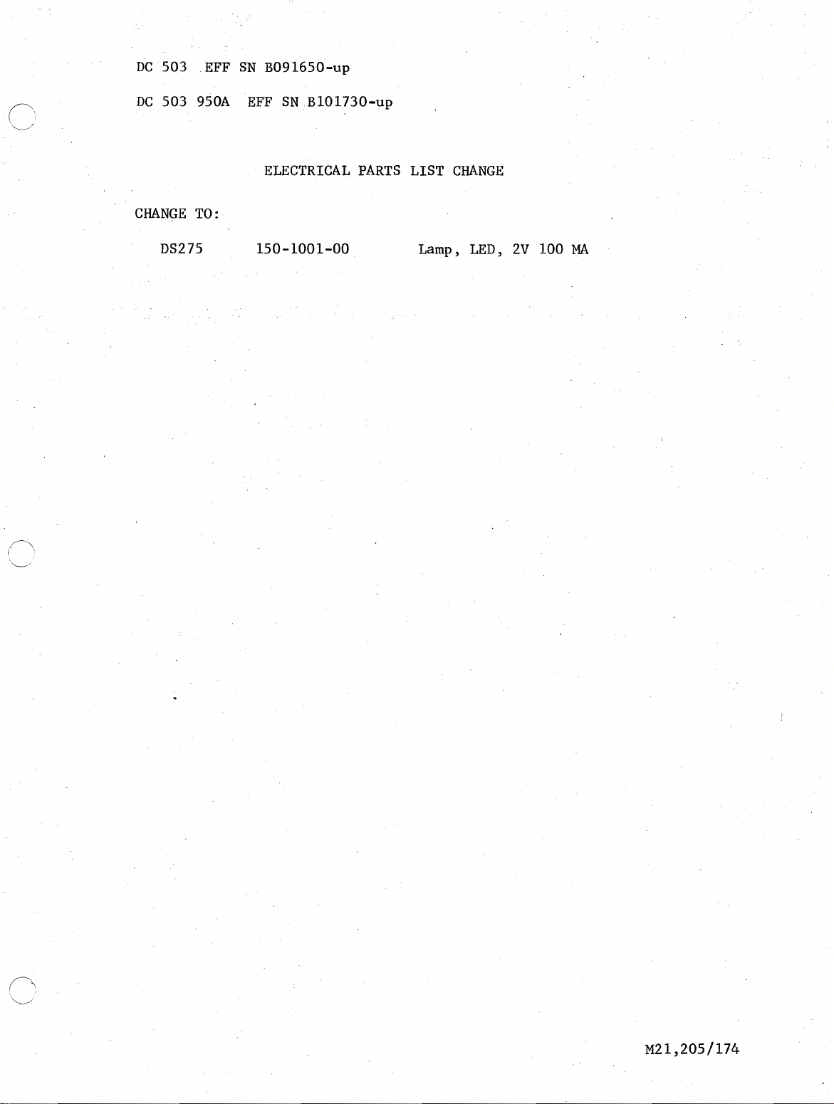
r'
DC
503
DC
503 950A
EFF
SN B091650-up
EFF
SN B101730-up
ELECTRICAL PARTS LIST
CHANGE
TO:
DS275 150- 1001-00
Lamp,
CHANGE
LED,
2V
100
MA
 Loading...