

Page 1
INSTRUCTION MANUAL
Qservice ----- This Document is a complete scan from the Original Tektronix Manual ----- Qservice
Tektronix, lnc.
070-141
2-00
-e
P.O. Box 500
+
Beaverton, Oregon 7005
+
Phone: 644-0161 + Cables: Tektronix
872
Page 2
Page 3
TABLE
Qservice ----- Hyperlinked Page Scroll Up - Down Left click to select ----- Qservice
Qservice ----- Hyperlinked Page Scroll Up - Down Left click to select ----- Qservice
OF
CONTENTS
Qservice
-----
SECTION
SECTION
HY per
1
2
linked Page Scroll Up - Down Left click to select
OPERATING INSTRUCTIONS Page
Introduction
Description
Installation
Operational Check
Display
Frequency Measurements
Totalizing
Using the Counter
Dl RECT INPUT Attenuation and Trigger
Signal Connection
Measurement
Rear Connector
Option 1-Precision Time Base
Specifications
THEORY OF OPERATION
Input Circuits
Time Base and Control Circuit
Counter Circuits
Decode and Display Multiplex
Power Supplies and InputIOutput Lines
Check
Level Adjustment
Interval and Display Time Controls
I10
Assignments
-----
Qservice
Qservice
SECTION
-----
SERVICE
3
Symbols
Electrical Parts List
Controls and Connectors Illustration
Adjustments Illustration
Parts Location Grid
Block Diagram
Counter Time Base and Control Schematic
Counters and Display Schematic
Mechanical Parts List
Fig.
Accessories
lNF ORMATION
&
Reference Designators
1
Exploded View
&
Repackaging
Hyperlinked Page Scroll Up - Down Left click to select
-----
Qservice
Page 4
Page 5
Section
Qservice ----- This Document is a complete scan from the Original Tektronix Manual ----- Qservice
1-DC
502
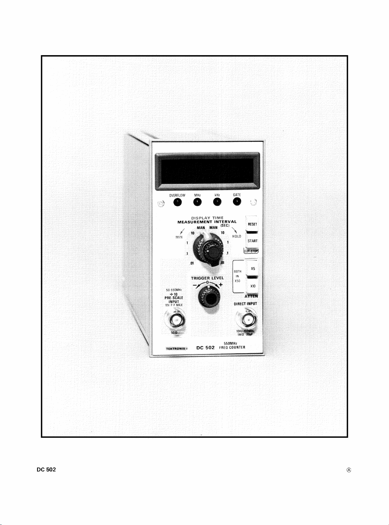
INTRODUCTION
Description
The DC 502 550 MHz Frequency Counter measures
frequencies from 10 Hz to 550 MHz or totalizes events to
10'
at
a
maximum rate of 550 MHz. The
in
a
TEKTRON
Frequency measurements are accomplished using one of
two BNC inputs on the front panel. The DIRECT INPUT
has a frequency range of 10 Hz to
peak-to-peak sensitivity, selectable attenuators, and an
adjustable trigger level range. The -10 PRE-SCALE INPUT
has
a
frequency range of 50 MHz to 550 MHz with
500 mV peak-to-peak sensitivity and
impedance. The same four measurement interval times are
selectable for each input.
IX
TM 500 Power Module only.
110 MHz with a 300 mV
DC
502 operates
a
50
i-2
input
SECTION
OPERATING
INSTRUCTIONS
Front panel controls reset the Counter and provide
Start/Stop commands for the manual totalizing mode of
each input.
Measurement display is accomplished with seven-segment
LED's in
automatically positioned by the MEASUREMENT
INTERVAL selected, and leading zeros (to the left of the
most significant digit or the decimal point) are blanked.
LED's indicate when the GATE is open, when the kHz or
MHz units are displayed, and when OVERFLOW occurs.
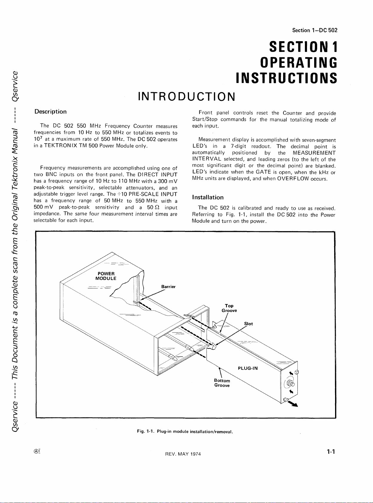
Installation
a
The
Referring to Fig.
Module and turn on the power.
a
7-digit readout. The decimal point is
DC
502 is calibrated and ready to use as received.
1-1, install the DC 502 into the Power
1
Fig.
1-1.
Plug-in module installation/removal.
REV.
MAY
1974
Page 6
Operating Instructions-DC
502
OPERATIONAL
Display Check
Press the RESET button to check the 7 character
segments of each digit; the numerical display should be a
row of eights. To check the decimal point position and the
units indicators,
switch as follows:
Switch
Position
In the MANUAL position, no decimal point will be
displayed. Press the START button and check that the
GATE indicator lights, then release the button (STOP) and
check that the GATE light goes out. To check the
OVERFLOW indicator,
INTERVAL switch to 10
INPUT connector. The length of time
is determined by the DISPLAY TlME control, and will be
discussed in the next few paragraphs.
set
the MEASUREMENT INTERVAL
Numerical
Display Units
.OOOO
.OOOOO
.OOO
.OOOO
000
000
.OOO
.OOOOO
.OOOO
.OOO
set
the MEASUREMENT
s
and apply 15- or 20-MHz to the
a
display can be held
MHz
MHz
kHz'
kHz
kHz
MHz
MHz
MHz
CHECK
Then turn the MEASUREMENT INTERVAL switch to the
position that gives the desired reading. Generally, use the
shorter measurement intervals for high-frequency, lowresolution measurements and the longer intervals for
measurements requiring
The OVERFLOW indicator can be lit for highresolution measurements, allowing the frequency to
be indicated to
the end of this secifion for resolution and accuracy at
each position of the MEASUREMENT INTER VAL
switch.
The display is updated at a rate determined by the
DISPLAY TlME control. Each time a sample of the input
signal
is
taken, the GATE light will flash and the new
reading will be displayed. To change the display time,
which is continuously variable from about 0.1 second to 10
seconds, or to hold a display indefinitely, turn the
DISPLAY TlME control.
+I0
Pre-Scale Input.
scaled, AC-coupled input to measure the average frequency
of signals from 50 MHz to 550 MHz. This input has
sensitivity of 500 mV, peak-to-peak, and a maximum input
voltage limit of 10
damage the diodes
may
10 V
ATTEN controls do not apply to this input.
a
high resolution.
NOTE
0, I Hz.
Refer to the Specifications at
The DC 502 also provides a pre-
\/,
peak-to-peak.
Signals greater than
of
the input circuit. The
a
Frequency Measurements
Direct Input.
of the average frequency of signals from about 10 Hz to
110 MHz. The input sensitivity is 300 mV peak-to-peak, so
select the proper attenuation (XI, X5, X10, or X50) for the
given signal.
The DC 502 provides direct measurement
CAUTION
a
The input signal must not exceed
a
Apply
MEASUREMENT INTERVAL switch to the .01 SEC position and the DISPLAY TlME control fully CCW. Observe
the numerical readout display. Adjust the TRIGGER
LEVEL control for
most significant digit in the display should be blanked.
signal to the INPUT connector. Set the
a
stable reading. The zeroes leading the
1-2
500
volts,
REV.
Apply a 50 MHz to 550 MHz signal of at least 500 mV
amplitude to the -10 PRE-SCALE INPUT. Set the
MEASUREMENT INTERVAL switch toJ .O1 SEC and
observe the readout. Leading zeros should be blanked.
Select a MEASUREMENT INTERVAL which gives the best
accuracy and resolution. As with the DIRECT INPUT,
shorter measurement intervals give higher frequency, lower
resolution measu rernents; longer intervals offer greater
resolution, especially when overflow is employed.
Totalizing
DIRECT INPUT.
accumulated number of signals (events) applied to the
DIRECT INPUT connector up to the register capacity of
9,999,999 during the time interval between STARTKTOP
commands from the front-panel pushbutton. Input signal
rate should not exceed 1 10 MHz.
MAY
The DC 502 will count and display the
Page 7
Operating Instructions-DC
502
Set the MEASUREMENT INTERVAL switch to
MANUAL, apply the signal, and push the START button.
The GATE indicator will light and the progressing count
will be displayed. Adjust the
LEVEL controls
the counting, release the START button. The GATE light
will go out and the displayed count will be held. The
displayed count can continue when the START button
depressed again. The counter can be cleared to zero
as
necessary for a steady count. To stop
ATTEN and TRIGGER
at
any
USING
THE
Dl R ECT l NPUT Attenuation and Trigger Level
Adjustment
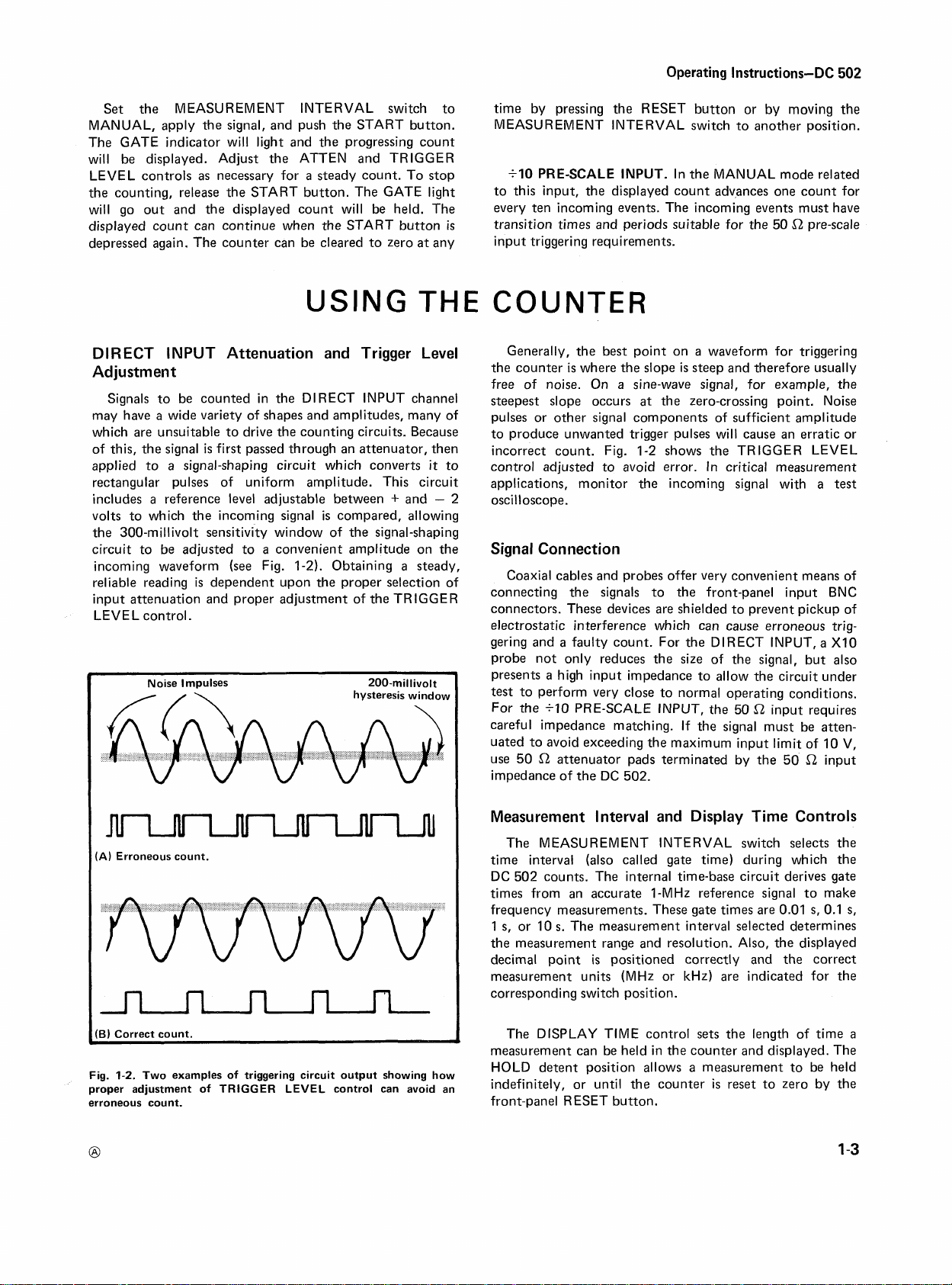
Signals to be counted in the DIRECT INPUT channel
a
may have
which are unsuitable to drive the counting circuits. Because
of this, the signal
applied to a signal-shaping circuit which converts
rectangular pulses of uniform amplitude. This circuit
includes
volts to which the incoming signal
the 300-millivolt sensitivity window of the signal-shaping
circuit to be adjusted to
incoming waveform (see Fig. 1-2). Obtaining
reliable reading
input attenuation and proper adjustment of the TRIGGER
,EVE L control.
wide variety of shapes and amplitudes, many of
is
first passed through an attenuator, then
a
reference level adjustable between + and
is
compared, allowing
a
convenient amplitude on the
a
steady,
is
dependent upon the proper selection of
Noise Impulses 200-millivolt
it
to
-
time by pressing the RESET button or by
MEASUREMENT INTERVAL switch to another position.
+I0
is
PRE-SCALE
to this input, the displayed count advances one count for
every ten incoming events. The incoming events must have
transition times and periods suitable for the
input triggering requirements.
INPUT.
In the MANUAL mode related
COUNTER
Generally, the best point on a waveform for triggering
the counter
free of noise. On
steepest slope occurs
pulses or other signal com ponents of sufficient amp1 itude
to produce unwanted trigger pulses will cause an erratic or
incorrect count. Fig. 1-2 shows the TRIGGER LEVEL
control adjusted to avoid error.
applications, monitor the incoming signal with
2
oscilloscope.
Signal Connection
Coaxial cables and probes offer very convenient means of
connecting the signals to the front-panel input BNC
connectors. These devices are shielded to prevent pickup of
electrostatic interference which can cause erroneous triggering and
probe not only reduces the size of the signal, but also
presents
test
to perform very close to normal operating conditions.
For the +10 PRE-SCALE INPUT, the 50
careful impedance matching. If the signal must be attenuated to avoid exceeding the maximum input limit of 10
use 50
impedance of the DC 502.
is
where the slope
a
sine-wave signal, for example, the
a
faulty count. For the DIRECT INPUT, a XI0
a
high input impedance to allow the circuit under
is
steep and therefore usually
at
the zero-crossing point. Noise
In critical measurement
s2
s2
attenuator pads terminated by the 50
moving
50
S2
input requires
the
pre-scale
a
test
V,
S'l
input
I
:A)
Erroneous count.
:B)
Correct count.
1-2.
Fig.
proper adjustment of TRIGGER LEVEL control can avoid an
erroneous count.
Two examples of triggering circuit output showing how
Measurement l nterval and Display Time Controls
The MEASUREMENT INTERVAL switch selects the
time interval (also called gate time) during which the
DC 502 counts. The internal time-base circuit derives gate
times from an accurate 1-MHz reference signal to make
frequency measurements. These gate times are 0.01
1
s,
or 10
s.
The measurement interval selected determines
the measurement range and resolution. Also, the displayed
is
decimal point
measurement units (MHz or kHz) are indicated for the
corresponding switch position.
The DISPLAY TIME control
measurement can be held in the counter and displayed. The
HOLD detent position allows
indefinitely, or until the counter
front-panel RESET button.
positioned correctly and the correct
sets
the length of time
a
measurement to be held
is
reset to zero by the
s,
0.1
s,
a
Page 8
Operating Instructions-DC
502
Fig.
1-3.
Input/Output pin assignments at rear connector.
Rear Connector I/O Assignments
lnput and output data access to the DC 502 is available
at the rear of the main circuit board. Fig. 1-3 identifies the
contacts and their respective
Module mainframe option is available which provides a
rear-panel, multi-pin connector to which these data can be
hard-wired for external access. Also possible are intracompartment connections with other plug-in modules when
using a multi-compartment Power Module.
1/0
assignments. A Power
Contact
28B
27 A
27 B
26A
25A
258
24B
23B
226
20 B
20A
21 B
19A
19B
1
Option
The DC 502 can be ordered with
compensated 5-MHz crystal oscillator to provide a highly
stable (5 parts in
option includes
1
-MHz clock.
-Precision Time Base
Second decimal point (D2) output.
Internal scan clock disable input.
MHz light output.
Reset inputloutput.
TSg (Time Slot Zero) output.
External scan clock input.
Internal scan clock (2 kHz) output.
Overflow output.
MSD (Most Significant Digit) output.
2
Data good output.
lo7)
and precise internal time base. This
a
divide-by-five IC counter to produce the
BCD output, serial by digit.
Assignment
a
temperature-
SPECIFICATIONS
Measurement Ranges, Resolution, and Accuracy
Frequency, 10 Hz to 550 MHz; Gate times, 0.01
1
s,
and 10
Totalizing capacity, 0 to
INPUT), 100 Hz
I
s,
INPUT), 1000 Hz
and 1 Hz at 10
s;
Display time, about 0.1 s to 10 s to HOLD;
at
0.01 s gate time, 10 Hz
and 0.1 Hz at 10
at
0.01
s;
Accuracy,
lo7;
Resolution (DIRECT
at
s;
Resolution (+I0 PRE-SCALE
sf
100 Hz
+I
at
0.1
s,
count + time base accuracy.
Direct lnput
Frequency, 10 Hz to 11 0 MHz; Sensitivity, 300 mV
peak-to-peak; Trigger level range, +2 V; Attenuators, XI,
X5, X10, and X50; Coupling, AC; lnput impedance,
approximately 1
input volts, 500 V (DC
+
10
Pre-Scale lnput
Frequency, 50 MHz to 550 MHz; Sensitivity, 500 mV
peak to peak; Coupling, AC; lnput impedance, approximately 50
Ma paralleled by about 20 bF; Maximum
+
peak AC, or peak-to-peak AC).
Q;
Maximum input volts, 10 V peak-to-peak.
Data Inputs and Outputs
Available via plug-in connector to multi-pin connector
rear of Power Module. lnput lines are available for internal
and external scan clock control. Output lines are available
for BCD output (serial-by-digit), and to indicate status of
timing, data good, reset, scale, decimal point and overflow.
0.1
10 Hz
s,
s,
1 Hz at
at
0.1
1
s,
s,
at
Internal Time Base
Option 1
5 MHz
Within 5 parts in
I
o7
1
part in
lo7
per month
within 5 parts in
1
lo9
Crystal Frequency
(OOC
Stability
+50°c), after
hour warm-up
Long-term Drift
Accuracy
to
I
/2
Standard
1 MHz
Within 1 part in
I
o5
1 part or less in
lo5
per month
Adjustable to Adjustable to
within 1 part in
1
lo7
Other
Temperature Range, Operating:
operating: -40°c to +75O~.
Altitude Range, Operating: to 15,000 feet; Non-
operating: 50,000 feet.
OOC
to +50°c; Non-
REV.
MAY
1974
Page 9
Section
Qservice ----- This Document is a complete scan from the Original Tektronix Manual ----- Qservice
2-DC
502
INPUT CIRCUITS
Direct lnput
Attenuators.
front-panel Dl R ECT INPUT connector J100 to the attenuators. The attenuators are frequency-compensated voltage
dividers consisting of resistors R 102-R
C102-C107. Switches SlOOA and SlOOB allow front-panel
selection of XI, X5, X10, or X50 attenuation of the input
signal. C110 provides AC coupling.
FET source follower Q115 and emitter follower 0122
present
the base circuit of E.
clamping network, which reduces the input signal to limits
suitable for driving the shaping circuits. The clamping
diodes limit the voltage
dynamic range of about 1.2 volts.
with push-pull outputs,
shapes the input signal into
window"
states
threshold, then reverts to
voltage passes through the lower threshold. For this reason,
an input signal smaller in amplitude than the width of the
hysteresis window cannot activate the counting circuits.
adjusted to overcome some of the triggering difficulties
arising from various input-signal shapes and frequencies.
Integrated-circuit operational amplifier U135 and
associated discrete components are connected
follower. TR IGGE R LEVEL potentiometer R 135 selects
voltage between ground and about -2 volts and applies
to pin 3 of U135. This level
hence, the input of U150B, through the action of the
operational amplifier.
a
Signal-Shaping.
when the signal voltage passes through the upper
The quiescent level at the input of U150B can be
Signals to be counted are applied via
107 and capacitors
high impedance to the input signal. The diodes in
F.
0128 form a series-limiter and
at
the emitter of 0128 to
U150B1 an OR gate integrated circuit
is
connected
a
is
a
width of about 200 mV. The output changes
its
is
as
a
Schmitt trigger. It
square wave. Its "hysteresis
original
then established
state
when the signal
as
a
at
pin 2, and
voltage
its
SECTION
THEORY
OPERATION
phase inversion (to correspond with the input signal) and
becomes the decade input.
+I
0
Pre-Scale lnput Circuit
50
MHz
to 550
AC-coupled into
current,
and 188 in the diode clamping bridge turned on until the
input signal amplitude reaches about
bridge
equivalent resistance of the bridge in series with R189,
2452, and the emitter resistance of Q190, about 552. As the
signal amplitude exceeds k0.4 V, one pair of diodes
(CR 185, CR 188) begins to turn off during positive-going
excursions, while the other pair (CR 186, CR 187) turns off
a
during negative-going excursions. As these diode pairs
alternately turn off with signal amplitude changes, a
matched pair of diodes
side of the coupling capacitor, C182, alternately turn on to
maintain the
CR181A
levels which may be part of the input signal.
changing DC level
peak-to-peak. This signal
via the high-frequency peaking network, C189-R189. C192
couples the amplified signal to pin 10, the high impedance
input of the +I0 counter, U190. C192
circuit board with special lead dress to aid high frequency
response
mounted on one lead of C192 to suppress high frequency
oscillations. R191 establishes
C191, 193, and 194 decouple pins 14, 13, and 12,
a
respectively, right
it
board. L199 and C199 suppress power supply noise and
decouple the Vcc input, pin 14.
set
by R185 and R187, keeps CR185, 186, 187
is
turned on, the signal source sees about 2052
&
CR181 B from being biased on or off by DC
The clamping action of the bridge diodes limits the
at
minimum signal amplitudes. Bead L192
MHz
signals applied to J180 are
a
5052 environment. A quiescent 10 mA
f0.4 V. While the
(CR181A, CR181 B) on the input
5052 input impedance. C181 prevents
at
the bridge output to a maximum 0.8 V
is
then coupled by C188 to Q190
is
mounted on the
a
bias
at
pin 10 of U190.
at
the terminal connections to the circuit
2
OF
is
Pin 4 of U190 produces one output cycle, a level change
The output of
push-pull outputs drive Q160 and Q162, which are connected
as
a
differential pair. This circuit provides a level shift
to TTL level, and further shapes the signal to be counted. A
waveform with fast rising and falling edges
the collector of Q160. CR165 limits the amplitude of the
count signal to 5 volts, clamping the negative-going portion
of the signal to ground. The signal
emitter follower 0170 to U160B, where
U150B
is
applied to U150A, whose
is
produced
is
then passed through
it
receives a final
at
of about 0.5 V, for every ten input events to pin 10. The
base of Q195 swings approximately between 3.4 V and
3.9 V. The emitter-follower action of 0195 provides
healthy current drive to the base of Q198, which would
saturate in no-signal conditions except for CR196. The
collector of
signal changes, producing
pin 9 of U16OB in the gating logic to the Decade Counting
Units.
Ql98 can, therefore, respond immediately to
a
TTL-compatible output to drive
a
Page 10

Theory of Operation-DC
TIME BASE AND CONTROL CIRCUIT
502
1
MHz
Clock
A precise one megahertz clock provides the reference for
operation of the gate-generating circuits. The output of
crystal oscillator Y 200
megahertz. The four parts of U200 form
is
adjustable by C201 to exactly one
a
shaper-buffer
stage to produce square-wave clock pulses and to isolate the
oscillator from the 1-MHz output line.
Optional Clock
An optional
5 MHz crystal oscillator and a divide-by-five counter. This
combination is shown on the schematic
1
MHz clock is available, using a very stable
as
Y201 and U201.
Decade Divider Units (DDU's)
The DDUrs consist of seven cascaded divided-by-ten
counters, U209 through U215. They produce four gate
times, 0.01 sec, 0.1 sec, 1 sec and 10 sec, which are made
available via the MEASUREMENT INTERVAL switch to
the gate generator to establish the precise time interval the
GATE is open. The
of U209, whose output
1-MHz
clock signal is applied to pin 14
is
connected to the input of the
subsequent decade. Each decade is clocked with a negativegoing transition. The DDUrs are reset by
which
a
count
in
U209
and
a
CLEAR pulse,
a
count
in
each
subsequent
Gate Generator
The gate generator produces the GATE control signal
and initiates the CLEAR, CLEAR, and LATCH pulses. The
generating portion consists of
U222B. The display time control portion consists of 0230,
Q238, and 0240. The circuit will be described first in the
normal gate mode (M EASU REM ENT INTERVAL switch in
one of the four gate time positions).
Assume that the To conditions are
The
Q
outputs of U220A, U222A, U220Br and U222B are
all LO. Q230
is
off and the emitter of 0238 rises
charges. At TI, Q238 reaches
discharges the capacitor. This results in
pulse on the direct-se_t input (pin 2) of U220A, forcing its Q
output
NAND gate
HI and its Q output LO. With two HI
U230A,
its
U220A, U222Ar U220B, and
as
given in Fig. 2-1.
as
C235
its
firing potential and
a
short-duration LO
inputs on
output goes LO and the output of
Scan Clock
Firing Potential
0238
Emitter
0240
Collector
U220A
0
U222A
0
U220B
0
U222B
0
-
0
CLEAR
LATCH
0238
Output
Output
Output
Output
Output
-
I
I
11
I
.
.
I (I I
I
II
Ill
I
'I
1
I'
I
II
I'
I I
I
II
I
Fig.
2-1.
I
1
I
I
I
I
I
I
I I
I
I Ill
I I
I
I
7-i
I I I
Time Base generator normal gating mode ladder diagram.
III
Ill
Ill
I
1
I I
I
I
I
I
I
Y
I
I
I
I]
1
I
I
I
I
I
I
I
I
I
I
I
I
I
I I
REV.
MAY
1974
Page 11
NOR gate U230C goes HI, producing the CLEAR and
CLEAR control signals. The next HI-to-LO transition from
the I-MHz
to go HI and
inputs, U230A reverts to
the CLEAR and CLEAR pulses. The DDUrs then start
counting from their 0999999 reset condition.
At the end of
DDU's to count the first digit, plus
negative transition from the DDU's via the MEASUREM ENT INTERVAL switch toggles U220B. This corresponds
T3 in Fig. 2-1. U220Brs Q output goes HI and
to
output goes
1-MHz clock (T4) toggles U2_22Br causing
go HI (GATE open) and
current to the front-panel GATE indicator LED, DS225).
The GATE signal
saturating the transistor and preventing C235 from
charging.
The GATE remains open (HI) for the time duration
selected by the MEASUREMENT INTERVAL switch. At
the end of this time, which corresponds to
another negative transition from the-DDU1s toggles U220B.
U220Brs Q output goes LO and
next negative transition from the 1-MHz clock (T6) toggles
U222BI causing
Simultaneously, the Q output goes HI, removing current
from the GATE indicator LED.
When the GATE output goes LO, the negative transition
toggles
U230D has two HI inputs, placing
gate U230B and activating the LATCH control signal (HI
clock-(T2) toggles U222A, causing
its
Q to go LO. With a LO applied to one of
its
original condition, terminating
a
10-microsecond delay (time for the
a
propagation delay), a
LO. The next negative transition from the
its
its
Q output to go LO (supplying
is
also applied to the base of 0230,
its
Q output goes HI. The
its
Output to go LO, closing the GATE.
U220A. switching Q LO and
a
HI.
Now NAND gate
a
LO
at
the input of OR
its
Q output
its
its
Q output to
T5 in Fig. 2-1,
Theory
state).
One microsecond later (T,),
the 1-MHz clock toggles U222A, switching
placing
reverts to
signal.
(T6). When 0230 turns off, C235 begins to charge through
R232-R235 toward the Vcc supply. R235, DISPLAY
TIME, provides an
display time from about 0.1 second to about 10 seconds.
When the DISPLAY TIME control
h
(HOLD detent position), S235 opens, and C235 stops
charging. When S235
sufficiently to bring Q238 to
display time ends and the next GATE-opening sequence
begins.
a
LO on the input of NAND gate U230D. U230D
its
original condition, terminating the LATCH
The display time begins when the GATE signal ends
adjustable time constant to vary the
is
of
Operation-DC
a
negative edge from
is
closed and C235 charges
its
firing potential (TI), the
Manual Gate
The manual mode of operation
MEASUREMENT INTERVAL switch in the MANUAL
position. The switch closure to ground (cam
switch) places
U222A, and
the
Q
outputs of U222A and U220B HI, and the Q output
of U220A LO. With both inputs of U230D held HI, the
LATCH output
the display continuously. The GATE
front-panel START button
applying
GATE-open condition
GATE
out). To reset the counters in the manual mode, the RESET
button must be pushed to activate to CLEAR, CLEAR and
RESET control signals.
is
a
LO on the set inputs of U220B and
a
LO on the clear input of U220A. This forces
is
held HI, allowing the counter to update
a
HI to the clear input of U222B. As before, the
is
HI
then closed when S210
is
selected by placing the
is
opened when the
is
pushed in, opening S210 and
at
the Q output of U222B. The
is
set
to STOP
502
its
outputs and
fully clockwise
5
of the
(button
COUNTER CIRCUITS
Decade Counter Units (DCU's)
The
lo0
through
divide-by-ten counters. The first decade counter
of four individual
decade input (up to 100 MHz), and each subsequent DCU
a
single IC. U165A, U165B, U167, and U169 comprise the
first (lo0) decade counter, and U235 through U240 make
up the remaining six DCUrs.
When the
the counter
toggle input of U165B. On every tenth clock input counted
by the first decade counter, the output of U169 goes LO,
providing
the second decade counter. Each subsequent decade divides
J
and K inputs of U165B are HI (GATE open),
is
enabled. The input signal
a
carry signal which becomes the clock input for
lo6
DCUrs are seven cascaded
J-K
flip-flops to accept the high-speed
is
applied to the
is
made up
by ten in
connected from each DCU to
latch. When the CLEAR (HI) and CLEAR (LO) signals are
activated, all of the decade counters are reset to the
zero-count
is
a
similar manner. Four BCD output lines are
its
associated storage-register
state.
Storage Register
The seven IC latches (U250 through U256) comprise
storage register which stores the corresponding decade
counter BCD output. The BCD output
data inputs
respectively). The LATCH
strobe input
closure of the GATE or when the MEASUREMENT
INTERVAL switch
at
pins
I,
5,
7,
and 3 (2O, 2l , 22, and 23 bits
pulse
at
pin 2 of each latch immediately upon
is
placed in the MANUAL position,
is
is
applied to the data-
a
applied to the
as
Page 12
Theory of Operation-DC
502
described in
LATCH input goes HI, the logic levels at the data inputs are
transferred to the associated BCD bit output to be scanned
by the multiplexing circuit.
the time base and control circuit. When the
Overflow Register
When the decade counters have counted to 9,999,999,
the counters are full. At the next count, the 23 output of
U240 goes LO, providing
this occurs,
U2416, then when the LATCH pulse ends (goes LO),
U241A
pin 13 of U241A goes LO, CR241 and DS242 conduct.
a
LO
is
is
toggled and the LO
a
toggle input to U241 B. When
transferred from pin 10 to pin 8 of
is
transferred to pin 13. When
DECODE AND DISPLAY MULTIPLEX
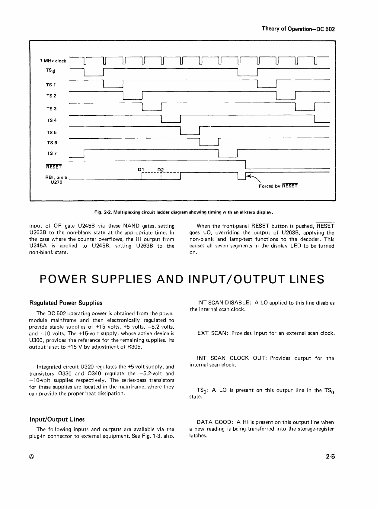
Scan Clock
The scan rate of the multiplexing circuit
by .the scan clock. The scan clock
and U260D, which operate
at
an approximate 2-kilohertz rate. The scan-clock output
passed through NOR gate U260A1 which can also accept an
externally applied scan-clock signal. Other inputloutput
lines provide internal scan-clock disable and internal scan-
clock output. The scan clock drives an eight-state counter
and
a
storage register for zero suppression.
+8
Counter and Time-Slot Decoder
The divide-by-eight counter
U263A, and U262A, which are three halves of SN7474
type D flip-flops. The output of this counter drives U265,
an SN74145 BCD-to-decimal decoder. U265 provides eight
output lines (designated TSo through TS7 in the schematics
and in Fig. 2-2) to simultaneously enable the output of
each counter latch and
sequentially. For example, when the TS1 line goes LO,
Q280
is
turned on to supply anode voltage to DS280
same time inverter U267C applies
U256, enabling
allows the latches to share
its
output. Operation in a time sequence
as
its
a
common
is
a
free-running multivibrator
is
made up of U2626,
corresponding display LED
a
HI to pin 6 of latch
set
is
determined
composed of U260B
at
the
of output lines.
DS242
front-panel OVERFLOW indication.
achieved via 0242 and CR244. The emitter of Q242
grounded by a switch closure, then when pin 9 of U241 B
goes HI on the first overflow count, 0242, CR244, and
DS242 turn on.
zero suppression during the overflow condition, the displaycontrolling circuits are notified via U245A that the count
in excess of that displayed by the LED readout.
is
an LED, and in
In the Manual counting mode, OVERFLOW indication
U241
is
reset by the CLEAR pulse. To prevent leading-
its
conduction state gives
Leading Zero Suppression
Decoder driver U270 also has a zero-blanking feature
which allows suppression of the zeroes leading the most
significant digit (MSD) in the display. At
is
applied to the direct-clear input of U2636, the zero-
suppression storage register. This sets U263B to the
zero-suppress state (HI at pin 8), allowing the RippleBlanking Input (RBI, pin 5) of U270 to be LO. When the
output of U265 advances to the next time slot
LO
RBI of U270 remains
propagation delays, which allows the first digit to arrive
frorn the latches while RBI
decoded
inhibited and the Ripple Blanking Output (pin 4) will be
LO. If the digit
RBO goes HI. The ,RBO
of U263B and
scan-clock HI-to-LO transition occurs. Thus, if the first
digit
output until the first non-zero digit comes through the
decoder. When the first non-zero digit arrives, the outputs
of U270 are enabled and the digit
RBO output
and allowing
the TS7 sequence.
is
a
zero, the output to the display LED will be
is
not a zero, the outputs are enabled and
is
transferred to the output when the next
is
a
zero, pin 5 of U270
at
pin 4
all
succeeding digits to be displayed through
for a few nanoseconds due to
is
LO. If this first digit being
is
applied to the D input (pin 12)
is
held LO, inhibiting the
is
displayed. Also, the
is
set HI, removing the RBI from pin 5
TSO,
a
(TS1
LO
),
a
is
is
is
is
the
Seven-Segment Decoder and Display LED's
U270
is a BCD-to-seven decoder.
output of the latches, then supplies current to the
appropriate cathodes of the enabled LED to display the
correct number. The display LED's are DS280 through
DS286. When looking
DS280 controls the numerical digit displayed
(lo6),
DS281 controls the second (1
seven segments, arranged so that
segments forms
lighted, an
"8"
is
at
the front panel of the DC 502,
a
number. When
formed.
It
accepts the BCD
at
the far left
o5
),
etc. Each LED has
a
combination of lighted
all
of the segments are
When the scan gets past the decimal point in the display,
or if the display overflows, any zeroes arriving
decoder should be displayed. This
TS5
is
inverted by U267E and applied through OR gate
U245B
pin 5 of U270 HI, preventing zero-blanking during the TS5,
TS6, and TS7 time slots. The location of the decimal point
in the display
INTERVAL switch. The proper information
the closed contacts of the switch to either NAND gate
U246A or U246B. Then either
as
a
LO
at
the direct-set input of U263B. This holds
is
determined by the MEASUREMENT
TS3
is
achieved
or
TS4
is
enabled to the
as
follows:
is
applied via
at
the
Page 13
1
MHz
clock
U
U
U
U
U
U
U
U
U
Theory
U
of
Operation-DC
U
502
RESET
RBI,
pin
5
U270
2-2.
Fig.
input of OR gate U245B via these NAND gates, setting
U263B to the non-blank
the case where the counter overflows, the HI output from non-blank and lamp-test functions to the decoder. This
U245A
non-blan k
is
applied to U245B, setting U263B to the causes
state.
state
Multiplexing circuit ladder diagram showing timing with an all-zero display.
at
the appropriate time. In goes LO, overriding the output of U263B, applying the
SUPPLIES
Regulated Power Supplies
The DC 502 operating power
module mainframe and then electronically regulated to
provide stable supplies of +I5 volts, +5 volts, -5.2 volts,
and -10 volts. The
U300, provides the reference for the remaining supplies. Its
output
is
set
+15-volt supply, whose active device
to
+I
5 V by adjustment of R305.
is
obtained from the power
Dl D2
r----
?----‘I
AND
,
When the front-panel RESET button
all
seven segments in the display LED to be turned
on.
I
Forced by RESET
-
is
pushed, RESET
LINES
INT SCAN DISABLE: A LO applied to this line disables
the internal scan clock.
is
EXT SCAN: Provides input for an external scan clock.
Integrated circuit U320 regulates the +5-volt supply, and
transistors 0330 and 0340 regulate the -5.2-volt and
-1 0-volt supplies respectively. The series-pass transistors
for these supplies are located in the mainframe, where they
can provide the proper heat dissipation.
Input/Output Lines
The following inputs and outputs are available via the
plug-in connector to external equipment. See Fig. 1-3, also.
INT SCAN CLOCK OUT: Provides output for the
internal scan clock.
TSO: A LO
state.
DATA GOOD: A HI
a
new reading
latches.
is
present on this output line in the TSo
is
present on this output line when
is
being transferred into the storage-register
Page 14

Theory of Operation-DC
502
OVERFLOW: This output
flows. digit, from the currently enabled storage-register latch.
RESET: This
provides a LO output during reset, or can be used as an
external reset input.
is
a dual-function input/output line.
is
HI when the count over-
It
Data Lines:
Other data lines include a LO when the MHz light
LO
when the second decimal point
left-side digit
1,
(MSD)
2,
4,
is
enabled.
8
provide BCD output, serial by
is
is
lit,
and a
HI
when the
on, a
----
Page 15

SERVICE
Qservice ----- This Document is a complete scan from the Original Tektronix Manual ----- Qservice
INFORMATION
w
,
DIAGRAMS, PARTS LISTS, AND ILLUSTRATIONS
Symbols
Electrical components shown on the diagrams are in the following units unless noted otherwise:
Symbols
Logic symbology is based on MIL-STD-806B in terms of positive logic. Logic symbols depict the logic function performed
and may differ from the manufacturer's data.
The following special symbols are used on the diagrams:
and
Reference Designators
used
on
the
diagrams are based
Capacitors
Resistors
on
ANSI
Values one or greater are in picofarads (pF).
=
Values less than one are in microfarads
=
Ohms
(a)
Y
32.2
-
1970.
External Screwdriver adjustment.
External control or connector.
Clockwise-control rotation in direction of arrow.
Refer to diagram number indicated in diamond.
Refer to waveform number indicated in hexagon.
(yF).
Connection soldered to circuit board.
Connection made to circuit board with interconnecting pin.
Blue tint encloses components located on circuit board.
P/Q
cimt
it
board
Page 16

RICAL PARTS LIST
Replacement parts should be ordered from the Tektronix Field Office or Representative in your area.
Changes to Tektronix products give you the benefit of improved circuits and components. Please include
the instrument type number and serial number with each order for parts or service.
ABBREVIATIONS AND REFERENCE DESIGNATORS
PTM
Assembly, separable or
A
repairable
Attenuator, fixed or variable
AT
Motor HR
B
Battery
BT
Capacitor, fixed or variable
C
Ceramic
Cer
Diode, signal or rectifier
CR
cathode-ray tube M
C RT
Delay line
DL
Indicating device (lamp)
D
S
Electrolytic P
Elect.
electrolytic, metal cased PMC
EMC
electrolytic, metal tubular PT
EMT
Fuse
F
Filter
F
L
Heat dissipating device
H
(
heat sink, etc.)
Heater
Connector, stationary portion
J
Relay
K
Inductor, fixed or variable
L
L
R
Inductor/resistor combination
Meter
Transistor or silicon-
Q
controlled rectifier
Connector, movable portion
Paper, metal cased
paper, tubular
paper or plastic, tubular
molded
Resistor, fixed or variable
R
Thermistor
RT
Switch
S
Transformer
T
Test point
TP
Assembly, inseparable or
u
non-repairable
Electron tube
v
Variable
Va r
Voltage regulator
V
R
etc.
1
wire-wound
WW
Crystal
Y
(zener diode,
Ckt. No.
ASSE LIES
?
A1
~ll
~1
A2
A3
A4
A5
CAPACITORS
l~tandard only.
2~ption
1
only.
Tektronix
Part No.
SerialIModel No.
Eff
BOlOlOO
B040000
Disc Description
B039999 HAIN Circuit Board Assembly
MAIN
Circuit Board Assembly
MAIN Circuit Board Assembly
DISPLAY Circuit Board Assembly
+
10 PRE-SCALER Circuit Board Assembly
PROTECTION Circuit Board Assembly
+
XB040000
5 Circuit Board Assembly
22 pF, Cer, 500
200 pF, Cer, 500
15 pF, Cer, 500
51
pF, Cer, 500
BOlOlOO
B050499 0.01 pF,
Cer,
B050500 0.01 pF, Cer, 500
BOlOlOO
B040502 0.01 pF, Cer, 500
B040503 0.01 pF, Cer, 500
82 pF, Cer, 500
0
.O1
pF,
Cer,
0.001 pF, Cer, 500
0.001 pF, Cer, 500
0.01 pF, Cer, 150
1
pF,
Cer,
25
0.001 uF, Cer, 500
170 pF, Cer, 500
1500 pF, Cer, 50
1500 pF,
Cer,
1500 pF, Cer, 50
1500 pF, Cer, 50
1500 pF,
Cer,
22 pF, Cer, 50
0.01 pF, Cer, 50
REV.
MAY
1974
V,
V
V,
V,
500
V,
V,
V,
V,
V,
150
V,
V,
V,
+80%-20%
V,
V,
50
V,
V,
V,
50
V,
V,
5%
V,
20%
10%
5%
+loo%-0%
20%
+loo%-0%
20%
20%
+80%-20%
V,
+loo%-0%
V,
+loo%-0%
+80%-20%
V,
+loo%-0%
5%
20%
20%
20%
20%
20%
20%
Page 17

ELECTRICAL PARTS LIST (cont)
Ckt Grid
No. Loc
CAPACITORS (cont)
Cl9 2
C193
Cl9 4
Cl9 6
C199
C200
C20
1
C202
C235
C252
C254
C256
C258
C2 60
C265
'
C267
C302
C305
C322
C325
C334
C335
C340
DIODES
CR115
CR122
CR124
CR125
CR127
CR128
CR165
Tektronix SerialIModel No.
Part No.
Eff
Disc Description
0.001 pF, Cer, 200
0.01 pF,
0.01 pF,
0.001 pF,
Cer,
Cer,
Cer,
150 pF, Elect.
10 pF,
Cer,
500
1.9-15.7 pF, Var,
18 pF,
Cer,
500
10 pF, Elect. , 25
100 pF,
Cer,
100 pF, Cer, 350
100 pF,
Cer,
100 pF, Cer, 350
50
50
,
350
350
200
6
V,
V
V,
V,
V,
Air
V,
V,
V,
V,
V,
V,
20%
20%
V,
20%
10%
20%
20%
20%
20%
20%
10%
10%
0.1 pF, Cer, 50V
Cer,
50
200
200
Cer,
25
V
500
V,
V,
V,
500
V,
+80%-20%
V,
V,
+loo%-0%
20%
5%
V,
20%
5%
V,
+loo%-0%
20%
0.1 pF,
0.001 pF,
Cer,
47 pF, Elect., 20
100 pF,
Cer,
100 pF, Elect, , 10
650 pF,
Cer,
0.001 pF,
1
pF,
Cer,
57 pF, Elect., 20
Silicon, replaceable by IN4152
Silicon, replaceable by IN4152
Silicon, replaceable by IN4152
Silicon, replaceable by IN4152
Silicon, replaceable by IN4152
Silicon, replaceable by IN4152
Silicon, replaceable by IN4152
Schottky barrier, matched pair
Silicon, replaceable by A1108
Silicon, replaceable by A1108
Silicon, replaceable by A1108
Silicon, replaceable by A1108
Silicon, replaceable by A1108
Silicon, replaceable by
IN4152
Silicon, replaceable by IN4152
Silicon, replaceable by IN4152
Zener, selected from 1N753A, 0.4
W,
6.2
V,
5%
INDICATORS
DS225 06
DS242 P6
DS280 N5
DS281 Q5
DS282 45
DS283 45
DS284 P5
DS285 P5
DS286 P5
DS290
DS292
FUSE
F320 R5
REV.
Lamp, light emitting diode, 2
Lamp, light emitting diode, 2
Numeric display, seven-segment
Numeric display, seven-segment, red
Numeric display, seven-segment, red
Numeric display, seven-segment, red
Numeric display, seven-segment, red
Numeric display, seven-segment, red
Numeric display, seven-segment, red
Lamp, light emitting diode, 2
Lamp, light emitting diode, 2
Cartridge, 2A, 3AG, f ast-blo
MAY
1974
V,
V,
,
V,
V,
70
70 mA
red
70 mA
70
mA
rnA
Page 18

ELECTRICAL PARTS LIST
(cont)
Ckt
Grid
Tektronix SerialIModel No.
No. Loc Part No.
INTEGRATED CIRCUITS (cont)
U241 G2
U245 52
CONNECTORS
JlOO
5180
INDUCTORS
L192 43
L199 42
TRANS ISTORS
Qll5
4122
4128
Q160
4162
4170
Q190
Ql9 5
Q
19 8
4230
4238
4240
Q242
4280
Q281
4282
Eff
Disc
Description
Dual 15
replaceable
Dual 4-input positive
by
Receptacle,
Receptacle,
Core, toroid ferrite
Toroid, 14 turns single
Silicon, FET, selected from
Silicon, PNP, replaceable by 2N4258
Silicon, NPN, selected from 2N3563
Silicon, NPN,
Silicon, NPN, replaceable by 2N3904 or TE3904
Silicon, PNP, replaceable by 2N4258
Silicon, PNP, replaceable by SMT1105
Silicon, NPN, replaceable by 2N3904 or TE3904
Silicon, NPN, selected from 2N3563
Silicon, NPN, replaceable by 2N3565
Silicon, unijunction, replaceable by 2N4851
Silicon, NPN, replaceable by 2N3565
Silicon, NPN, replaceable by 2N3565
Silicon, PNP, replaceable by 2N3907
Silicon, PNP, replaceable by 2N3907
Silicon, PNP, replaceable by 2N3907
MHz
SN7425N
J-K
master-slave flip-flop
by
SN7473N
nor
gates, replaceable,
electrical,
electrical,
replaceable
BNC,
BNC, female
2N4392
by 2N3904
female
or
TE3904
4283
4284
4285
4286
4320
Q33Q
4340
RES
ISTORS
R102
R10
R10
R107
R112
R113
R115
R117
R118
R120
R121
R122
R123
R126
R12 7
R130.
R132
R135
R137
Rl3 7
R139
R140
Silicon, PNP, replaceable by 2N3907
Silicon, PNP, replaceable by 2N3907
Silicon, PN?, replaceable by 2N3907
Silicon, PNP, replaceable by 2N3907
V,
Thyristor, 50
Eilfcon,
Silicon, PNP, replaceable
3
PNP,
8A, replaceable
replaceable
bv
b$-
by
2N4249
2N4249
2N4441
6
W,
W,
1/2
W.
W,
W,
W.
5%
5%
5%
5%
5%
IZ
2 kR, 114
1
kR, 114
W2,
10
2C
B029999 51 kQ, 1/4
51
10
950
114
kG.
Var
kQ , (nominal value) , selected
'kR, 114
kQ,
@
REV.
MAY
1974
Page 19

Tektronix SerialIModel No.
Ckt. No. Part No.
ELECTRICAL PA-RTS LIST
Eff
Disc Description
(cont)
RESISTORS
R152
R153
R155
R158
R159
R162
R16 3
R165
R167
R169
R172
R173
R175
R177
R181
R184
R185
R187
R188
R189
R190
Rl9
R19 2
R19 2
~19 2l
~-19 2l
R19
Rl9 4
Rl9 6
R19 8
R200
R203
R205
R209
R220
R222
R224
R226
R230
R232
~23.5~
R238
R240
R242
(cont)
-
1
3
315-0203-00
315-0221-00
315-0561-00 B0 60000
315-0221-00 BOlOlOO B049999
315-0561-00 B050000
315-0101-00
315-0332-00
315-0303-00
315-0122-00
315-0181-00
315-0242-00
315-0271-00
315-0301-00
315-0562-00
315-0562-00
315-0562-00
315-0301-00
315-0562-00
315-0202-00
311-1342-00
315-0100-00
315-0102-00
315-0562-00
BOlOlOO
B059999
20
kR,
220
560
220
560
loo
3.3
kQ,
30
1.2
180
2.4
270
300
5.6
5.6
5.6
300
5.6
2
kR,
500
10
a,
1
kR,
5.6
n,
$2,
a,
n,
n,
kn,
kf2,
a,
kR,
n,
Q,
kn,
kQ,
kfi,
R,
kR,
114
kfi,
114
114
kR,
114
114
114
114
114
114
114
1/4
1/4
114
114
114
1/4
114
114
1/4
114
1/4
Var
1/4
W,
w,
W,
W,
w,
w,
W,
W,
W,
W,
W,
w,
W,
W,
W,
W,
W,
W,
W,
W,
W,
W,
5%
5%
5%
5%
5%
5%
5%
5%
5%
5%
5%
5%
5%
5%
5%
5%
5%
5%
5%
5%
5X
5%
R244
R260
R261
R264
R265
R267
R271
1.
,Option
1
only.
*-Furnished as a unit
wdZh
S235.
REV.
MAY
1974
Page 20

ELECTRICAL PARTS LIST
(cont)
Ckt
No. Loc
RESISTORS
Grid
(cont)
Tektronix Serial/Model No.
Part
No.
Eff
Disc
BOlOlOO B049999
B050000
BOlOlOO B039999
B040000
BOlOlOO B049999
B050000
BOlOlOO B039999
B040000
300
a
1
kn
300
n
1
ksl
300
n
1
kS2
300
S2
1
kn
150
a,
n,
150
!2,
150
300
Q,
n,
300
R,
5.6
3.3
kR,
1
kn, Var
3
kR,
620
R,
620
a,
1.5
kfi,
56
S2,
R, 2 W,
120
0,
56
n,
120
kR,
1
0.3
Q,
1.6
kR,
4.99
2.49
Q,
160
4.53
15.8
kQ,
2
9.31
15.8
100
a,
56
n,
100
n,
n, 2 w,
56
Thick film, 7 section divider
114
W,
5%
114
W,
5%
114
W,
5%
114
W,
5%
1.14
w,
5%
114
W,
5%
114
W,
5%
114
W,
W,
W,
114
W,
5%
5%
5%
W,
10%
5%
2
2
2
10%
2
W,
10%
2
w,
10%
114
W,
10%
3
W,
WW,
W,
W,
W,
W,
W,
W,
5%
W,
W,
5%
10%
5%
1%
5%
1%
1%
5%
1%
1%
1%
1%
kfi,
kn,
kR,
kn,
114
kR,
kR,
2
114
118
118
114
118
118
W,
118
118
2
W,
w,
2
W,
10%
'standard only.
:option
>~urnished as a unit with
1
only.
R235.
REV.
Pushbut ton,
Actuator assembly
START
Push,
RESET
MAY
1974
x10
ATTENUATOR X5
,
MEASUREMENT INTERVAL
Page 21

ELECTRICAL
PARTS
LIST
(cont)
Ckt
No.
Grid
Loc
Tektronix SeriallModel No.
Part No.
INTEGWTED CIRCUITS
L~tandard only.
1
2~ption
only.
Eff
XI3040000
XB040000
BOlOlOO
BOlOlOO
B060000
BOlOlOO
BO
10 100
B060000
Disc
B039999X
B059999
B039999X
B059999
Dual 100
replaceable by SN74S112N
Quad 2-input nand gate, replaceable by SN74SOON
Operational amplifier, replaceable by UA741C
Type 2-3-2 input gate, replaceable by MC10105
Quad 2-input nand gate, replaceable by SN74SOON
Dual 100
placeable by SN74S112
Single 40
replaceable by SN74H102
Single 40
replaceable by SN74H102
Single 40
replaceable by SN74H102
Single 40
replaceable by SN74H102
Single 40
replaceable by SN74H102
Single 40
replaceable by SN74H102
Divide by 10 ctr, replaceable by SP630B
Quad 2-input positive nand gate, replaceable
by
Single 10
replaceable by SN7490N
Single 10
replaceable by SN7490N
Single 10
replaceable by SN7490N
Single 10
replaceable by SN7490N
Single 10
replaceable by SN7490N
Single 10
replaceable by SN7490N
Single 10
replaceable by SN7490N
Single 10
replaceable by SN7490N
Dual 15
replaceable by SN7476N
Dual 20
replaceable by SN74111N
Quad 2-input positive nand buffer, replaceable
by SN7437N
Single 10
replaceable by SN7490N
Single 10
replaceable by SN7490N
Single 10
replaceable by SN7490N
Single 10
replaceable by SN7490N
Single 10
replaceable by SN7490N
Single 10
replaceable by SN7490N
SN7400N
MHz
MHz
MHz
J-K
mas ter-slave flip-flop,
MHz
J-K
master-slave flip-flop, re-
MHz
J-K
edge-triggered flip-flop,
MHz
J-K
edge-triggered flip-flop,
MHz
J-K
edge-triggered flip-flop,
MHz
J-K
edge-triggered flip-flop,
MHz
J-K
edge-triggered flip-flop,
MHz
J-K
edge-triggered flip-flop,
MHz
divide-by-2-&-5 ripple counter,
MHz
divide-by-2-&-5 ripple counter,
MHz
divide-by-2-&-5 ripple counter,
MHz
divide-by-2-&-5 ripple counter,
MHz
divide-by-2-&-5 ripple counter,
MHz
divide-by-2-&-5 ripple counter,
MHz
divide-by-2-&-5 ripple counter,
MHz
divide-by-2-&-5 ripple counter,
J-K
master-slave flip-flop,
J-K
mas ter-slave flip-flop,
MHz
divide-by-2-&-5 ripple counter,
MHz
divide-by-2-&-5 ripple counter,
MHz
divide-by-2-&-5 ripple counter,
MHz
divide-by-2-&-5 ripple counter,
MHz
divide-by-2-&-5 ripple counter,
MHz
divide-by-2-6-5 ripple counter,
REV.
MAY
1974
Page 22

Tektronix Serial/Model No.
Ckt. No. Part No.
Eff
ELECTRICAL PARTS LIST (cont)
Disc Description
INTEGRATED CIRCUITS (cont)
U246
U250
U251
U252
U253
U254
U255
U256
U260
U262
U263
U265
U267
U270
U300
U320
CRYSTALS
Y2OO1
Y
201
Quad 2-input positive nor gate, replaceable by
SN7402N
Quad latch, replaceable by MC4035P
Quad latch, replaceable by MC4035P
Quad latch, replaceable by MC4035P
Quad latch, replaceable by MC4035P
Quad latch, replaceable by MC4035P
Quad latch, replaceable by MC4035P
Quad latch, replaceable by MC4035P
Quad 2-input positive nand gate, replaceable
by SN7400N
MHz
Dual 15
replaceable by SN7474N
Dual 15
replaceable by SN7474N
Single BCD-to-decimal decoder/driver,
replaceable by SN74145N
Hex. inverter, replaceable by SN7404N
Single BCD-to-seven-segment decoderldriver,
replaceable by SN7447N
Voltage regulator, replaceable by UA723C
Voltage regulator, replaceable by UA723C
Crystal,
Oscillator,
D-type pos-edge-trig flip-flop,
MHz
D-type pos-edge-trig flip-flop,
1
MHz
RF,
5
MHz
loption 1 only.
Page 23

Time-Base Frequency Check and Adjustment. Connect
the
DC
502
1-MHz time base reference and the secondary
standard to the oscilloscope as shown. Adjust the oscilloscope to display several complete cycles.
To determine oscillator error, observe the rate of
horizontal drift of the displayed waveform. Waveform
moving to the right indicates that the time-base frequency
is
<I
MHz; to the left,
the waveform to move the width of one cycle
the frequency difference in parts in
the waveform drifts to the right at
10
width every
lo6
in
part in
Adjust
low. Maximum allowable frequency difference
lo5
C201
seconds, the time-base frequency
(5
parts in
for no drift.
>
1
~~z./?he period in secondsfor
lo6.
For example, if
a
rate of one cycle's
lo7
for the optional
5
MHz
is
equal to
is
0.1
crystal).
part
is
CONTROLS AND CONNECTORS
1
Page 24

INTERNAL ADJUSTMENTS PROCEDURE
Services
adjustment
Service Center. Contact your local TEKTRON l
Office or representative for further information.
Available
Tektronix, I nc. provides complete instrument repair and
at
local Field Service Centers and at the Factory
X
Field
Test Equipment
For measurement of the power supply voltages, a 20,000
ohms/volt
example, Triplett 630 NA multimeter.
For 1-MHz frequency measurement,
frequency standard or other frequency source having
stability of
measuring optional
for accuracy. Also recommended
a
bandwidth of
for frequency-comparison measurement.
VOM
will give satisfactory measurements. For
at
least 5 parts on
5
MHz crystal output)
at
least 1 MHz and a stable triggering circuit
lo7
(5 parts in
is
is a test oscilloscope with
a
secondary
lo8
recommended
if
Procedure
If
NOTE
The performance of this instrument can be check at
any temperature within the
Make any adjustment at a temperature between
+20"~
TM 500 Series Power'Module or connected
extender (TEKTRON IX Part No. 067-0645-01
a
and
+30°C (+68"~
The DC 502 can be operated either fully
and
O"C
+86"
to
F).
+50°c
range.
installed in a
1
to a plug-in
I.
the instrument is operated on the plug-in extender,
the +5-volt supply may not regulate,
Secondary
Standard
0
Power
voltmeter between the +15-volt test point and ground.
Adjust R305 for a reading of
+5-volt, -5.2-volt, and -10-volt supplies to be within
Supply Checks and Adjustment. Connect the
+I5 volts. Then check the
5%.
NOTE
1
MHz
1
MHz
Vert
Input
I
Time-Base Frequency Check and Adjustment. Connect
the DC 502 1-MHz time base reference and the secondary
standard to the oscilloscope as shown. Adjust the oscilloscope to display several complete cycles.
To determine oscillator error, observe the rate of
horizontal drift of the displayed waveform. Waveform
moving to the right indicates that the time-base frequency
is
<I
MHz; to the left,
the waveform to move the width of one cycle
the frequency difference in parts in
the waveform drifts to the right
width every 10 seconds, the time-base frequency
in
lo6
low. Maximum allowable frequency difference
lo5
(5
part in
Adjust C201 for no drift.
parts in 10' for the optional 5 MHz crystal).
>
1
~~z./?he period in secondsfor
lo6.
For example, if
at
a
rate of one cycle's
is
equal to
is
0.1 part
is
1
-5.2
V
R330
Test,
+I5
V
Adjust
Page 25

PARTS
LOCAT ION
GRID
*See
Parts
serial number ranges.
COMPONENTS
List for
SHOWN
WlTH
DASHED
*
R307 added to backside of board SN 8050000-up.
LINES
ARE LOCATED
ON
BACK SIDE
OF
BOARD.
Relocated on back
R139 of board SN B070000.
REV.
MAY
1974
@
Page 26

OPTIONAL
OSC
SEE PARTS LIST FOR EARLIER
VALUES AND SERIAL NUMBER
RANGES
WITH
BLUE
ILLATOU
OF
PARE MARKED
OUTLINE.
LATCH
-
T;zps
=
@
1
15
VOLTS '15V
+s
VOLTS
+5V
i6
SWITCH
DSTENT
110
DIPECT
PIIE-SCALC
r
INPUT
L
r
INPUT
L
5W
FCW
1111
11 10
13 11
MEASUREMENT
ID0
XNTERVAL
I
6
I
I
I
2
f
I
I
I
5
Page 27

SIGNAL-SHAPING
Cl RCUlT
+I0 PRE-SCALE
I
INPUT
1
)+I
INPUT Q115 U135 Q162
1
-MHz CLOCK
I
Y200
r
PTTIONA
1-MHz
I
CLOCK
Y201
U201
I-------
REGULATED
I
C
CR185 Q190 Q195
CR186 U190 Q198
CR187 U 160C
CR188
SIGNAL-SHAPING
0122 U150A 0160
0128 U150B 0170
I
K""'"
UNITS -01SEC
U209
u210
u211
I
U212
U213 ,I0 SEC
U214
1
-1 SEC
1
1
SEC
DC
502
BLOCK DIAGRAM
I
STEERING
1
DISPLAY TIME
CONTROL
0230 0238
0240
-
t
GATEGENERATOR GATE
U220A U222A LATCH
U220B U222B
--
-
- - -
CONTROL SIGNALS'
U230A U246D
U230B RESET
U23QC
U230D
INTER
SWITCH
- - -
A
7
-
CLEAR
-
CLEAR
-
4
I
I
L
7
LATCH
DCU
DCU
I
STORAGE
ZEGISTER
10" DCU
10' DCU
lo5
U239
lo6
U240
----I
t
OVERFLOW
1
U260A U262A DECODER
U260B U262B
U260D U263A
4 BCD OUTPUT LINES
U250
U251
U252
U253
U254
U255
U256
RESET
LEADING-ZERO
-?-
SUPPRESSION
DECIMAL POINT
1
1
INVERTERS
U246C U267D
U267A U267E
U267B U267F
4
U267C
&
LOCATION
U245B
U246A
I
A
6 TIME-SL
LINES
TS, -TS,
DISPLAY
i
ANODE
VOLTAGE
ENABLE
Q280 Q281 Q282 0283 0284 0285
SEGMENT
DECODER
7
segment
lines
LED'S
DS280
DS281
DS282
DS283
DS284
DS285
DS286
1
-5.2 V REG
-10 V REG
Page 28

IER
lBER
ED
Page 29

Fig.
Qservice ----- This Document is a complete scan from the Original Tektronix Manual ----- Qservice
Index
No.
ABBREVIATIONS
BHB
BHS
C
csk
D
FHB
FHS
Fil HB
Fil HS
&
Tektronix
Part
MECHANICAL PARTS LIST
Replacement parts should be ord,ered from the Tektronix Field Office or Representative in your area.
Changes to Tektronix products give you the benefit of improved circuits and components.
the instrument type number and serial number with each order for parts or service.
binding head brass
binding head steel
RT
E
cathode-ray tube
countersunk
double end
flat head brass
flat head steel
fillister head brass
fillister head steel
h
hex.
HHB
HHS
HSB
HSS
ID
1
g
OD
height or high
hexagonal
hex head brass
hex head steel
hex socket brass
hex socket steel
inside diameter
length or long
outside diameter
OHB
OHS
PHB
PHs
RHS
SE
TH B
THS
W
Q
t
Description
No.
Serial/Model
Eff
No.
Disc
Please include
oval head brass
oval head steel
pan head brass
pan head steel
round head steel
single end
truss head brass
truss head steel
wide or width
KNOB,
gray- -TRIGGER LEVEL
knob includes:
SETSCREW, 5-40 x 0.125 inch, HSS
KNOB,
red--DISPLAY TIME
knob includes:
SETSCREW, 5-40 x 0.125 inch, HSS
KNOB, gray- -MEASUREMENT INTERVAL
knob includes:
SETSCREW, 5-40
KNOB,
latch
PUSHBUTTON- -RESET
x
0.125 inch, HSS
.
PUSHBUTTON--START
PUSHBUTTON--X5
PUSHBUTTON--XI0
CONNECTOR, receptacle,
wlhardware (See
JlOO
&
BNC,
5180 electrical list)
mounting hardware for each: (not included w/connector)
ID,
TERMINAL, lug, 0.391 inch
SE
RESISTOR, variable (See R135 electrical list)
mounting hardware: (not included with resistor)
NUT, hex., 0.25-32 x 0.312 inch
WASHER, flat, 0.25
ID
x 0.375 inch
OD
FRAME, pushbutton
FRAME, readout window
WINDOW,
readout
SHIELD, electrical, side
PANEL, front
mounting hardware: (not included with panel)
SCREW, 2-56 x 0.375 inch,
x
NUT, hex., 2-56
0.188 inch
PHs
Page 30

Mechanical Parts List-DC
502
FIGURE
Fig.
&
Index Tektronix SerialIModel No. t
No. Part No.
Eff
Disc
-
-
1
EXPLODED (cont)
Q
Y
12345
.-
--
-
LATCH, plug-in retaining
mounting hardware: (not included with latch)
SCREW, thread forming, 2-56 x 0.25 inch, 100° csk, FHS
SUBPANEL, front
mounting hardware: (not included wlsubpanel)
SCREW, thread forming, 6-20 x 0.375 inch, 100° csk, FHS
CIRCUIT BOARD ASSEMBLY--DISPLAY (See A2 electrical list)
SHIELD, electrical,
CIRCUIT BOARD ASSEMBLY--PRESCALER (See A3 electrical list)
circuit board assembly includes:
SOCKET, integrated circuit, 14 pin
SOCKET, pin connector
mounting hardware: (not included
SCREW, 2-56 x 0.25 inch,
CIRCUIT BOARD ASSEMBLY--MAIN (See
circuit board assembly includes:
CONTACT, electrical (For repair, see maint. section)
SOCKET, pin connector
SOCKET, pin connector
LINK, terminal connecting
COUPLING, shaft
coupling includes:
SETSCREW, 4-40
RING, coupling
COUPLING, plastic
SHAFT, extension
SWITCH, push--START-STOP (S235)
SPACER, switch, brown
SWITCH, push--ATTEN (S100A
RESISTOR, variable (See R235 electrical list)
mounting hardware: (not included
NUT,
hex., 0.25-32 x 0.312 inch
WASHER, lock, internal, 0.261
BRACKET, component mounting
mounting hardware: (not included wlcircuit board assy)
SCREW, thread forming, 6-20
Description
subpanel
PHs
x
0.188 inch, HSS
&
x
wlcircuit board assy)
A1
electrical list)
S100B)
w,/resistor)
ID
x
0.40 inch
0.312 inch, PHs
OD
Page 31

FIGURE 1 EXPLODED (cont)
Fig.
&
Q
index Tektronix SerialIModel No. t Description
No. Part No.
Eff
Disc
-
-
y
-
12345
-
-
-
-
-
-
--
1
FRAME SECTION, bottom
1
FRAME SECTION, top
1
WIRING HARNESS
1
ACTUATOR ASSEMBLY, cam switch (S200)
-
actuator assembly includes:
1
-
2 SCREW, 2-56
2 WASHER, lock, internal, 0.092
1
-
-
-
1
1
1
2 NUT, hex., 2-56 x 0.188 inch
4 NUT, hex., 4-40
-
3
COVER
mounting hardware: (not included with cover)
1
RING, retaining
BEARING, front
SPRING, flat,
SPRING, flat, green
SPRING, flat, red
ROLLER, det ent
DRUM ASSEMBLY
BEARING, rear
mounting hardware: (not included wlactuator assembly)
SCREW, sems, 4-40 x 0.312 inch, PHB
-
--
--
x
0.188 inch, PHs (Discard & use ref #28)
gold
x
0.188 inch
Mechanical Parts
ID
x
0.18 inch
List-DC
OD
502
1
CIRCUIT
-
2 CLIP, electrical, fuse
-
1
1
circuit board assembly includes:
mounting hardware: (not included wlcircuit board assy)
SCREW, thread forming, 6-32 x 1.25 inches, PHs
SPACER, sleeve, 0.986'inch long
BOARD
ASSEMBLY--PROTECTION (See A4 elect. list)
1
Replace only with part bearing the same color code as the original part in your instrument.
Page 32

This Document was scanned from the original
Tektronix Service Manual
For enquiries about high quality technical manuals
Qservice@otenet.gr
This Document is a complete Scan from the original
Tektronix manual
For enquiries about our complete
High quality line of technical Manuals in PDF
mailto : Qservice@otenet.gr
Page 33

DC
502 550
MHz
FREQUENCY COUNTER
Page 34

ACCESSORIES
Fig.
&
Index Tektronix SeriaIIModel No.
No. Part No. Eff Disc
2
-
070-1412-00
0
t
y
1
1
2 3 4
MANUAL,
5
instruction (not shown)
Description
REPACKAGING
DC
502-550MHz
FREQUENCY COUNTER
Fig.
&
Index Tektronix SerialIModel No.
No.
Part No. Eff Disc
t
y
1
2
3
4
5
1
CARTON ASSEMBLY
carton assembly includes:
2
1
1
1
1
FRAME
END CAP,
END CAP,
PAD
SET,
CARTON
front
rear
1
piece
Description
Page 35

MANUAL CHANGE INFORMATION
Qservice ----- This Document is a complete scan from the Original Tektronix Manual ----- Qservice
At Tektronix, we continually strive to keep up with latest
electronic developments by adding circuit and component
improvements to our instruments as soon as they are developed and tested.
Sometimes, due to printing and shipping requirements, we
can't get these changes immediately into printed manuals.
Hence, your manual may contain new change information on
following pages.
A single change may affect several sections. Sections of
the manual are often printed at different times, so some of
the information on the change pages may already be in
your manual. Since the change information sheets are carried
in the manual until ALL changes are permanently entered,
If
some duplication may occur.
in this section, your manual is correct as printed.
no such change pages appear
Page 36

This Document was scanned from the original
Tektronix Service Manual
For enquiries about high quality technical manuals
Qservice@otenet.gr
This Document is a complete Scan from the original
Tektronix manual
For enquiries about our complete
High quality line of technical Manuals in PDF
mailto : Qservice@otenet.gr
Page 37

TEXT
CORRECT
ION
The upper
been changed to 110
limit
MHz.
frequency response specifications has
be changed to read: 110
Any reference to a 100
MHz.
MHz
should
Page 38

This Document was scanned from the original
Tektronix Service Manual
For enquiries about high quality technical manuals
Qservice@otenet.gr
This Document is a complete Scan from the original
Tektronix manual
For enquiries about our complete
High quality line of technical Manuals in PDF
mailto : Qservice@otenet.gr
Page 39

DC
DC
501
502
EFF
EFF
SN
B040000-up
SN
B040000-up
Page
1
of
2
REMOVE
U167
U169
CHANGE
A1
ADD
:
u1
U2
ELECTRICAL PARTS LIST
:
156 -0100 -00
156 -0100 -00
TO:
670-2102-01
670-3300 -00
156-0118-00 Dual 100
156-0180-00 Quad 2-input nand gate, replaceable by
AND
SCHENATIC CHANGES
Single 40
MHz
J-K
replaceable by SN74H102
MHz
Single 40
J-K
replaceable by SN74H102
MAIN
DIVIDE
Circuit Board Assembly
BY
5,
Circuit Board Assembly
MHz
J-K
replaceable by SN74S112
SN74SOON
edge-triggered flip-flop,
edge-triggered flip-flop,
master-slave flip-flop,
,
Page 40

Page
Page 41

DC
DC
501
502
EFF
SN
B060000-up
EFF
SN R070000-up
ELECTRICAL
CHANGE
ADD
(R137
TO:
R137 311-1554-00 200
:
C121 283-0111-00 0.1
and
C121
are
PARTS
located
LIST
on
AND
Diagram
SCHEMATIC
kfl,
Var
pF,
Cer, 50
1
COUNTER TIME
0
CHANGE
V
BASE
&
CONTROL)
A
PARTIAL-
Page 42

This Document was scanned from the original
Tektronix Service Manual
For enquiries about high quality technical manuals
Qservice@otenet.gr
This Document is a complete Scan from the original
Tektronix manual
For enquiries about our complete
High quality line of technical Manuals in PDF
mailto : Qservice@otenet.gr
 Loading...