

Page 1

Instruction Manual
R
DAS
/TLA LADM935
SBus Bus Support
070-9609-00
There are no current European directives that
apply to this product. This product provides cable
and test lead connections to a test object of
electronic measuring and test equipment.
Warning
The servicing instructions are for use by qualified
personnel only. To avoid personal injury, do not
perform any servicing unless you are qualified to
do so. Refer to all safety summaries prior to
performing service.
Online Version: April 1997
Page 2

Copyright E Tektronix, Inc. All rights reserved. Licensed software products are owned by Tektronix or its suppliers and
are protected by United States copyright laws and international treaty provisions.
Use, duplication, or disclosure by the Government is subject to restrictions as set forth in subparagraph (c)(1)(ii) of the
Rights in T echnical Data and Computer Software clause at DFARS 252.227-7013, or subparagraphs (c)(1) and (2) of the
Commercial Computer Software – Restricted Rights clause at F AR 52.227-19, as applicable.
T ektronix products are covered by U.S. and foreign patents, issued and pending. Information in this publication
supercedes that in all previously published material. Specifications and price change privileges reserved.
Printed in the U.S.A.
T ektronix, Inc., P.O. Box 1000, Wilsonville, OR 97070–1000
TEKTRONIX, TEK,, and DAS are registered trademarks of T ektronix, Inc.
Page 3

HARDWARE WARRANTY
T ektronix warrants that the products that it manufactures and sells will be free from defects in materials and
workmanship for a period of one (1) year from the date of shipment. If a product proves defective during this
warranty period, T ektronix, at its option, either will repair the defective product without charge for parts and labor,
or will provide a replacement in exchange for the defective product.
In order to obtain service under this warranty, Customer must notify Tektronix of the defect before the expiration
of the warranty period and make suitable arrangements for the performance of service. Customer shall be
responsible for packaging and shipping the defective product to the service center designated by T ektronix, with
shipping charges prepaid. Tektronix shall pay for the return of the product to Customer if the shipment is to a
location within the country in which the T ektronix service center is located. Customer shall be responsible for
paying all shipping charges, duties, taxes, and any other charges for products returned to any other locations.
This warranty shall not apply to any defect, failure or damage caused by improper use or improper or inadequate
maintenance and care. T ektronix shall not be obligated to furnish service under this warranty a) to repair damage
resulting from attempts by personnel other than T ektronix representatives to install, repair or service the product;
b) to repair damage resulting from improper use or connection to incompatible equipment; c) to repair any
damage or malfunction caused by the use of non-T ektronix supplies; or d) to service a product that has been
modified or integrated with other products when the effect of such modification or integration increases the time
or difficulty of servicing the product.
THIS WARRANTY IS GIVEN BY TEKTRONIX IN LIEU OF ANY OTHER WARRANTIES, EXPRESS
OR IMPLIED. TEKTRONIX AND ITS VENDORS DISCLAIM ANY IMPLIED WARRANTIES OF
MERCHANTABILITY OR FITNESS FOR A PARTICULAR PURPOSE. TEKTRONIX’
RESPONSIBILITY TO REPAIR OR REPLACE DEFECTIVE PRODUCTS IS THE SOLE AND
EXCLUSIVE REMEDY PROVIDED TO THE CUST OMER FOR BREACH OF THIS WARRANTY.
TEKTRONIX AND ITS VENDORS WILL NOT BE LIABLE FOR ANY INDIRECT , SPECIAL,
INCIDENTAL, OR CONSEQUENTIAL DAMAGES IRRESPECTIVE OF WHETHER TEKTRONIX OR
THE VENDOR HAS ADVANCE NOTICE OF THE POSSIBILITY OF SUCH DAMAGES.
Page 4

SOFTWARE WARRANTY
T ektronix warrants that the media on which this software product is furnished and the encoding of the programs on
the media will be free from defects in materials and workmanship for a period of three (3) months from the date of
shipment. If a medium or encoding proves defective during the warranty period, T ektronix will provide a
replacement in exchange for the defective medium. Except as to the media on which this software product is
furnished, this software product is provided “as is” without warranty of any kind, either express or implied.
T ektronix does not warrant that the functions contained in this software product will meet Customer’s
requirements or that the operation of the programs will be uninterrupted or error-free.
In order to obtain service under this warranty, Customer must notify Tektronix of the defect before the expiration
of the warranty period. If T ektronix is unable to provide a replacement that is free from defects in materials and
workmanship within a reasonable time thereafter, Customer may terminate the license for this software product
and return this software product and any associated materials for credit or refund.
THIS WARRANTY IS GIVEN BY TEKTRONIX IN LIEU OF ANY OTHER WARRANTIES, EXPRESS
OR IMPLIED. TEKTRONIX AND ITS VENDORS DISCLAIM ANY IMPLIED WARRANTIES OF
MERCHANTABILITY OR FITNESS FOR A PARTICULAR PURPOSE. TEKTRONIX’
RESPONSIBILITY TO REPLACE DEFECTIVE MEDIA OR REFUND CUSTOMER’S PAYMENT IS
THE SOLE AND EXCLUSIVE REMEDY PROVIDED TO THE CUSTOMER FOR BREACH OF THIS
WARRANTY. TEKTRONIX AND ITS VENDORS WILL NOT BE LIABLE FOR ANY INDIRECT,
SPECIAL, INCIDENTAL, OR CONSEQUENTIAL DAMAGES IRRESPECTIVE OF WHETHER
TEKTRONIX OR THE VENDOR HAS ADVANCE NOTICE OF THE POSSIBILITY OF SUCH
DAMAGES.
Page 5

Table of Contents
General Safety Summary iii. . . . . . . . . . . . . . . . . . . . . . . . . . . . . . . . . . . . . . . . . . .
Service Safety Summary v. . . . . . . . . . . . . . . . . . . . . . . . . . . . . . . . . . . . . . . . . . .
Preface: Microprocessor Support Product Documentation vii. . . . . . . .
Manual Conventions vii. . . . . . . . . . . . . . . . . . . . . . . . . . . . . . . . . . . . . . . . . . . . . .
Logic Analyzer Documentation viii. . . . . . . . . . . . . . . . . . . . . . . . . . . . . . . . . . . . . .
Getting Started 1. . . . . . . . . . . . . . . . . . . . . . . . . . . . . . . . . . . . . . . . . . . .
Product Description 1. . . . . . . . . . . . . . . . . . . . . . . . . . . . . . . . . . . . . . . . . . . . . . .
Logic Analyzer System Software Compatibility 1. . . . . . . . . . . . . . . . . . . . . . . . .
Logic Analyzer Configuration 2. . . . . . . . . . . . . . . . . . . . . . . . . . . . . . . . . . . . . . .
Requirements and Restrictions 2. . . . . . . . . . . . . . . . . . . . . . . . . . . . . . . . . . . . . . .
Configuring the Probe Adapter 2. . . . . . . . . . . . . . . . . . . . . . . . . . . . . . . . . . . . . .
Connecting to a System Under T est 3. . . . . . . . . . . . . . . . . . . . . . . . . . . . . . . . . . .
Setting Up the Application 6. . . . . . . . . . . . . . . . . . . . . . . . . . . . . . . . . . .
Channel Group Definitions 6. . . . . . . . . . . . . . . . . . . . . . . . . . . . . . . . . . . . . . . . .
Clocking Options 6. . . . . . . . . . . . . . . . . . . . . . . . . . . . . . . . . . . . . . . . . . . . . . . . .
Symbols 7. . . . . . . . . . . . . . . . . . . . . . . . . . . . . . . . . . . . . . . . . . . . . . . . . . . . . . . .
Acquiring and Viewing Disassembled Data 10. . . . . . . . . . . . . . . . . . . . .
Acquiring Data 10. . . . . . . . . . . . . . . . . . . . . . . . . . . . . . . . . . . . . . . . . . . . . . . . . . .
Viewing Disassembled Data 10. . . . . . . . . . . . . . . . . . . . . . . . . . . . . . . . . . . . . . . .
Hardware Display Format 10. . . . . . . . . . . . . . . . . . . . . . . . . . . . . . . . . . . . . . .
Software Display Format 12. . . . . . . . . . . . . . . . . . . . . . . . . . . . . . . . . . . . . . .
Control Flow Display Format 12. . . . . . . . . . . . . . . . . . . . . . . . . . . . . . . . . . . .
Subroutine Display Format 12. . . . . . . . . . . . . . . . . . . . . . . . . . . . . . . . . . . . . .
Changing How Data is Displayed 12. . . . . . . . . . . . . . . . . . . . . . . . . . . . . . . . . . . .
Optional Display Selections 12. . . . . . . . . . . . . . . . . . . . . . . . . . . . . . . . . . . . .
Marking Cycles 13. . . . . . . . . . . . . . . . . . . . . . . . . . . . . . . . . . . . . . . . . . . . . . .
Viewing the Reference Memory 13. . . . . . . . . . . . . . . . . . . . . . . . . . . . . . . . . . . . .
Specifications 14. . . . . . . . . . . . . . . . . . . . . . . . . . . . . . . . . . . . . . . . . . . . . .
Probe Adapter Description 14. . . . . . . . . . . . . . . . . . . . . . . . . . . . . . . . . . . . . . . . . .
Channel Assignments 15. . . . . . . . . . . . . . . . . . . . . . . . . . . . . . . . . . . . . . . . . . . . . .
How Data is Acquired 20. . . . . . . . . . . . . . . . . . . . . . . . . . . . . . . . . . . . . . . . . . . . .
SBus Clocking 20. . . . . . . . . . . . . . . . . . . . . . . . . . . . . . . . . . . . . . . . . . . . . . .
Alternate Connections 21. . . . . . . . . . . . . . . . . . . . . . . . . . . . . . . . . . . . . . . . . . . . .
Signals Not On the Probe Adapter 21. . . . . . . . . . . . . . . . . . . . . . . . . . . . . . . .
Extra Acquisition Channels 22. . . . . . . . . . . . . . . . . . . . . . . . . . . . . . . . . . . . .
Maintenance 23. . . . . . . . . . . . . . . . . . . . . . . . . . . . . . . . . . . . . . . . . . . . . . .
Replacing Signal Leads 23. . . . . . . . . . . . . . . . . . . . . . . . . . . . . . . . . . . . . . . . . . . .
Replacing Protective Sockets 23. . . . . . . . . . . . . . . . . . . . . . . . . . . . . . . . . . . . . . . .
Replaceable Parts 24. . . . . . . . . . . . . . . . . . . . . . . . . . . . . . . . . . . . . . . . . .
Parts Ordering Information 24. . . . . . . . . . . . . . . . . . . . . . . . . . . . . . . . . . . . . . . . .
Using the Replaceable Parts List 25. . . . . . . . . . . . . . . . . . . . . . . . . . . . . . . . . . . . .
LADM935 SBus Support Instruction Manual
Online Version
i
Page 6

Table of Contents
List of Figures
List of Tables
Figure 1–1: Connecting podlets to the SBus probe adapter 4. . . . . . . .
Figure 1–2: Placing the SBus probe adapter onto the SUT 5. . . . . . . . .
Figure 1–3: Hardware display format 11. . . . . . . . . . . . . . . . . . . . . . . . . .
Figure 1–4: Minimum clearance of the probe adapter 15. . . . . . . . . . . .
Figure 1–5: SBus bus timing 21. . . . . . . . . . . . . . . . . . . . . . . . . . . . . . . . . .
Figure 1: Sbus probe adapter exploded view 27. . . . . . . . . . . . . . . . . . . .
Table 1–1: Control group symbol table definitions 7. . . . . . . . . . . . . . .
Table 1–2: Size group symbol table definitions 7. . . . . . . . . . . . . . . . . .
Table 1–3: Ack group symbol table definitions 8. . . . . . . . . . . . . . . . . .
Table 1–4: IntReq group symbol table definitions 8. . . . . . . . . . . . . . .
Table 1–5: Cycle type definitions 11. . . . . . . . . . . . . . . . . . . . . . . . . . . . .
Table 1–6: LADM935 PhysAddr group channel assignments 16. . . . . . .
Table 1–7: LADM935 Data group channel assignments 17. . . . . . . . . . .
Table 1–8: LADM935 Control group channel assignments 18. . . . . . . .
Table 1–9: LADM935 Size group channel assignments 18. . . . . . . . . . .
Table 1–10: LADM935 Ack group channel assignments 19. . . . . . . . . .
Table 1–11: LADM935 IntReq group channel assignments 19. . . . . . . .
Table 1–12: LADM935 Misc group channel assignments 20. . . . . . . . . .
Table 1–13: LADM935 clock channel assignments 20. . . . . . . . . . . . . . .
Table 1–14: Extra acquisition module sections and channels 22. . . . . . .
ii
LADM935 SBus Support Instruction Manual
Online Version
Page 7

General Safety Summary
Review the following safety precautions to avoid injury and prevent damage to
this product or any products connected to it.
Only qualified personnel should perform service procedures.
While using this product, you may need to access other parts of the system. Read
the General Safety Summary in other system manuals for warnings and cautions
related to operating the system.
Injury Precautions
Product Damage
Precautions
Avoid Electric Overload. To avoid electric shock or fire hazard, do not apply a
voltage to a terminal that is outside the range specified for that terminal.
Avoid Electric Shock. To avoid injury or loss of life, do not connect or disconnect
probes or test leads while they are connected to a voltage source.
Ground the Product. This product is indirectly grounded through the grounding
conductor of the mainframe power cord. To avoid electric shock, the grounding
conductor must be connected to earth ground. Before making connections to the
input or output terminals of the product, ensure that the product is properly
grounded.
Do Not Operate in Wet/Damp Conditions. To avoid electric shock, do not operate
this product in wet or damp conditions.
Do Not Operate in an Explosive Atmosphere. To avoid injury or fire hazard, do not
operate this product in an explosive atmosphere.
Avoid Exposed Circuitry. To avoid injury, remove jewelry such as rings, watches,
and other metallic objects. Do not touch exposed connections and components
when power is present.
Use Proper Power Source. Do not operate this product from a power source that
applies more than the voltage specified.
Do Not Operate With Suspected Failures. If you suspect there is damage to this
product, have it inspected by qualified service personnel.
LADM935 SBus Support Instruction Manual
Online Version
iii
Page 8
General Safety Summary
Symbols and Terms
T erms in this Manual. These terms may appear in this manual:
WARNING. Warning statements identify conditions or practices that could result
in injury or loss of life.
CAUTION. Caution statements identify conditions or practices that could result in
damage to this product or other property.
T erms on the Product. These terms may appear on the product:
DANGER indicates an injury hazard immediately accessible as you read the
marking.
WARNING indicates an injury hazard not immediately accessible as you read the
marking.
CAUTION indicates a hazard to property including the product.
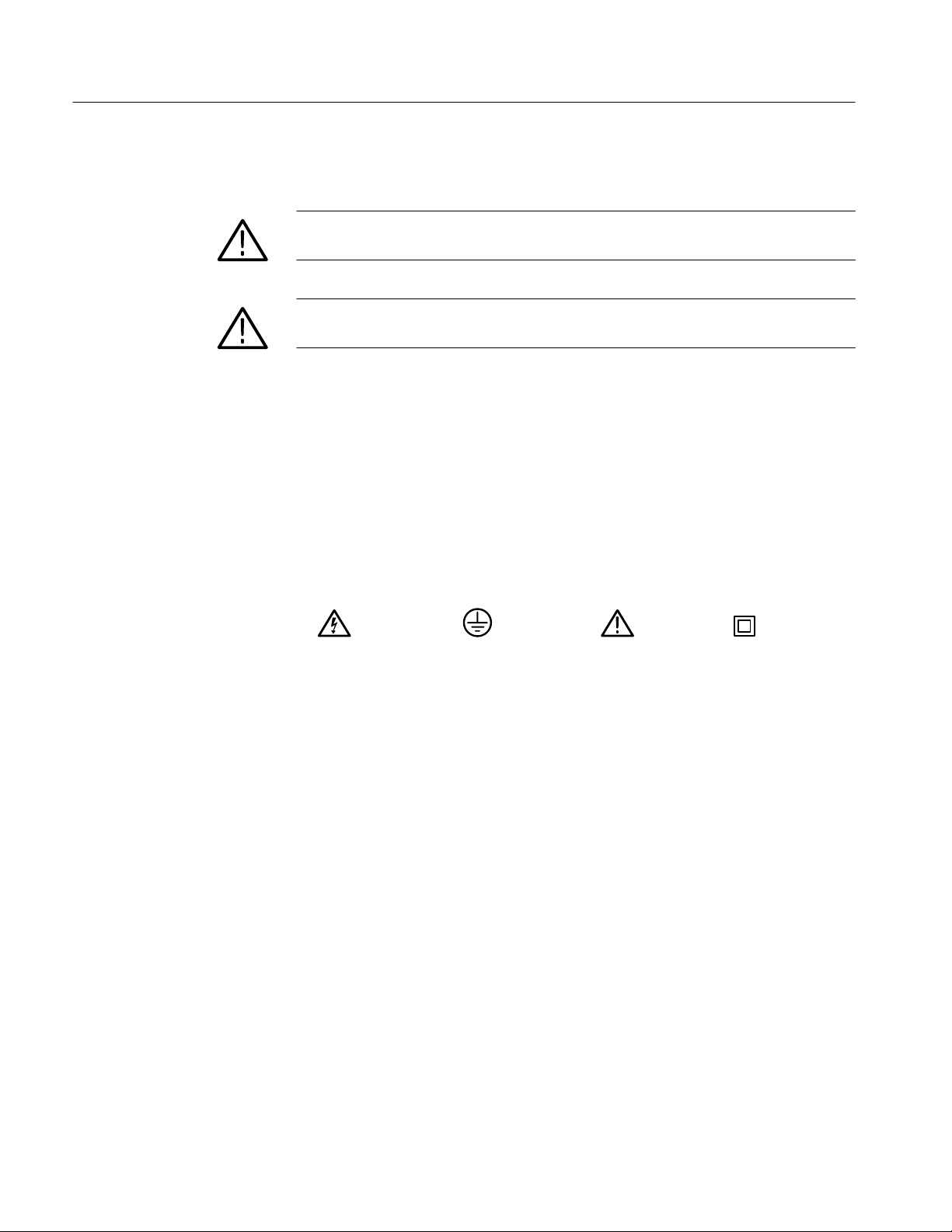
Symbols on the Product. The following symbols may appear on the product:
DANGER
High Voltage
Protective Ground
(Earth) T erminal
ATTENTION
Refer to Manual
Double
Insulated
iv
LADM935 SBus Support Instruction Manual
Online Version
Page 9

Service Safety Summary
Only qualified personnel should perform service procedures. Read this Service
Safety Summary and the General Safety Summary before performing any service
procedures.
Do Not Service Alone. Do not perform internal service or adjustments of this
product unless another person capable of rendering first aid and resuscitation is
present.
Disconnect Power. To avoid electric shock, disconnect the main power by means
of the power cord or, if provided, the power switch.
Use Care When Servicing With Power On. Dangerous voltages or currents may
exist in this product. Disconnect power, remove battery (if applicable), and
disconnect test leads before removing protective panels, soldering, or replacing
components.
To avoid electric shock, do not touch exposed connections.
LADM935 SBus Support Instruction Manual
Online Version
v
Page 10

Preface: Microprocessor Support Product Documentation
This instruction manual is part of a two-manual set for operating bus support
products on compatible Tektronix logic analyzers and contains specific information about the SBus support product. If you are familiar with operating support
products on the logic analyzer for which this product was purchased, you
probably only need to use this instruction manual to successfully operate the
product.
One or more basic operations user manuals are included with bus support
products. Each logic analyzer has its own basic operations manual that describes
how to perform tasks common to bus support products on that platform. You
should place the appropriate basic operations user manual in the notebook behind
this instruction manual.
If you are not familiar with operating bus support products on a Tektronix logic
analyzer, you will need to use the basic operations user manual with this
instruction manual to operate the SBus support product.
This manual provides detailed information on the following topics:
H
Connecting the logic analyzer to the system under test
Manual Conventions
H
Setting up the logic analyzer to acquire data from the system under test
H
Acquiring and viewing disassembled data
H
The LADM935 probe adapter
This manual uses the following conventions:
H
The term disassembler refers to the application software that disassembles
bus cycles into instruction mnemonics and cycle types.
H
The term SUT (system under test) refers to the bus-based system from which
data is being acquired.
H
The term logic analyzer refers to the Tektronix logic analyzer for which this
product was purchased.
H
The term acquisition module refers to the 92A96 data acquisition modules.
H
The term 92A96 refers to all versions of the 92A96, 92C96, and subsequent
DAS/TLA acquisition modules unless otherwise noted.
LADM935 SBus Support Instruction Manual
Online Version
vii
Page 11

Preface: Microprocessor Support Product Documentation
H
The term XXX or P54C used in field selections and file names in the basic
operations user manual can be replaced with SBus. This is the name of the
bus in field selections and file names you must use to operate the support
product.
H
A tilde (~) following a signal name indicates an active low signal.
Also refer to the Glossary in the basic operations user manual for definitions of
logic analyzer, acquisition module, and disassembler terms.
Logic Analyzer Documentation
A description of other documentation available for each type of Tektronix logic
analyzer is located in each basic operations user manual. The documentation
provides the information necessary to install, operate, maintain, and service the
logic analyzer and associated products.
viii
LADM935 SBus Support Instruction Manual
Online Version
Page 12
Getting Started
Product Description
The DAS/TLA LADM900 series of support products are developed by third
parties to support buses, microprocessors, microcontrollers, and digital signal
processors for specific Tektronix customers. These support products are currently
being successfully used by these customers. If you need assistance in using this
product, contact your local Tektronix Technical Support Specialist.
This chapter provides information on the following topics:
H
The LADM935 SBus support product
H
Logic analyzer system software compatibility
H
Your SBus system requirements
H
SBus support product restrictions
H
How to connect to your SUT (system under test)
The SBus Bus Support product disassembles data from systems based on SUN
SPARC Technology microSPARC-II microprocessors (manufactured by Fujitsu)
using SBus protocol. The instruction mnemonics are based on the SPARC
Version 8 instruction set. The LADM935 product runs on a DAS/TLA logic
analyzer equipped with at least one 92A96 Data Acquisition Module.
A complete list of accessories and options is provided at the end of the parts list
in the Replaceable Parts chapter.
To use this product efficiently, you need to have the items listed in the basic
operations user manual as well as the IEEE Standard for a Chip and Module
Interconnect Bus (IEEE Std 1496-1993), IEEE, 1993.
Logic Analyzer System Software Compatibility
The label on the application floppy disk states which version of logic analyzer
system software the application is compatible with.
LADM935 SBus Support Instruction Manual
Online Version
1
Page 13

Getting Started
Logic Analyzer Configuration
To use the SBus support product, the logic analyzer must be equipped with at
least one 92A96 module and four standard data acquisition probes.
The basic operations user manual contains information on how to configure the
DAS/TLA under Configuring the Logic Analyzer in the Getting Started chapter.
Requirements and Restrictions
You should review the general requirements and restrictions of bus support
products in the Getting Started chapter in the basic operations user manual as
they pertain to your SUT:
You should also review the mechanical specifications in the Specifications chapter
in this manual as they pertain to your system under test, as well as the following
description of other SBus support product requirements and restrictions.
9201T DAS System. If you have a 9201T version of the DAS/TLA system, you
must change the system to the 92XTerm or 9202XT version.
Burst Reads and Burst Writes. For Burst Reads and Burst Writes, the calculated
address following the rules of Sub-Block Ordering are not supported.
64-Bit Extended Transfers. The 64- bit extended transfers are not supported.
Disabling the Instruction and Data Caches. To disassemble acquired data, you
must disable the internal instruction and data caches on the microSPARC-II
microprocessor. Disabling the cache makes all instruction prefetches visible on
the SBus bus so they can be acquired and disassembled.
Configuring the Probe Adapter
The probe adapter does not require any configuration.
2
LADM935 SBus Support Instruction Manual
Online Version
Page 14

Connecting to a System Under Test
Before you connect to the SUT, you must connect the standard probes to the
acquisition module. Your SUT must also have a minimum amount of clear space
surrounding the SBus connector to accommodate the probe adapter. Refer to the
Specifications chapter in this manual for the required clearances.
The Requirements and Restrictions description in the basic operations user
manual shows the vertical dimensions of an acquisition probe connected to
square pins on a circuit board.
To connect the DAS to the SUT, follow these steps:
1. Turn off power to your SUT. It is not necessary to turn off power to the DAS.
CAUTION. Static discharge can damage the microprocessor, the probe adapter,
the podlets, or the 92C96 Module. To prevent static damage, handle all of the
above only in a static-free environment.
Getting Started
Always wear a grounding wrist strap or similar device while handling the probe
adapter.
2. To discharge your stored static electricity, touch the ground jack located on
the back of the DAS. Then, touch any of the ground pins of the probe
adapter to discharge stored static electricity from the probe adapter.
3. Connect the 92C96 clock and 8-channel probes to the probe adapter as
shown in Figure 1–1. Match the channel groups and numbers on the probe
interface housing to the corresponding pins on the probe adapter. Match the
ground pins on the probes to the corresponding pins on the probe adapter.
LADM935 SBus Support Instruction Manual
Online Version
3
Page 15

Getting Started
Hold the 8-Channel probes by the podlet
holder when connecting them to the
probes adapter. Do not hold them by the
cables or necks of the podlets.
8-Channel probes
Clock probes
Prode adapter
Figure 1–1: Connecting podlets to the SBus probe adapter
4. Align pin 1 on the probe adapter connector with pin 1 on the connector in
your SUT and connect the two together as shown in Figure 1–1.
4
LADM935 SBus Support Instruction Manual
Online Version
Page 16

Pin 1
Getting Started
SUT socket
Figure 1–2: Placing the SBus probe adapter onto the SUT
LADM935 SBus Support Instruction Manual
Online Version
5
Page 17

Setting Up the Application
This section provides information on how to set up the application. Information
covers the following topics:
H
Channel group definitions
H
Clocking options
H
Symbol table files
Remember that the information in this section is specific to the operations and
functions of the LADM935 SBus bus support product on any Tektronix logic
analyzer for which it can be purchased. For information on general tasks and
functions, refer to the basic operations user manual.
Before you acquire and disassemble data, you need to load the application and
specify setups for clocking, and triggering as described in the basic operations
user manual. The application provides default values for each of these setups,
but you can change them as needed.
Channel Group Definitions
Clocking Options
The application automatically defines channel groups for the support product.
The channel groups for the SBus bus are PhysAddr, Data, Control, Size, Ack,
IntReq, and Misc. If you want to know which signal is in which group, refer to
the channel assignment tables beginning on page 15.
The LADM935 application offers a bus-specific clocking mode for the SBus bus.
This clocking mode is the default selection whenever you select SBus Support in
the 92A96 Configuration menu.
The LADM935 application acquires all SBus cycles. No clocking options are
available.
A description of how cycles are sampled by the acquisition module using the
LADM935 application and probe adapter is found in the Specifications chapter.
Disassembly
The basic operations user manual contains information on how to use these other
clock selections with any bus support package in the Reference chapter under
General Purpose Analysis.
will not be correct with the Internal or External clocking modes.
6
LADM935 SBus Support Instruction Manual
Online Version
Page 18

Setting Up the Application
Symbols
Disassembly
will not be correct with the Internal or External clocking modes.
The basic operations user manual contains information on how to use these other
clock selections with any bus support package in the Reference chapter under
General Purpose Analysis.
The LADM935 application supplies four symbol table files. The SBus_Ctrl file
replaces specific Control channel group values with symbolic values when SYM
or PATTERN is the radix for the channel group.
Table 1–1 shows the name, bit pattern, and meaning for the symbols in the file
SBus_Ctrl, the Control channel group symbol table.
T able 1–1: Control group symbol table definitions
Control group value
BR~ Sel~
Symbol
WRITE XXX X0X
READ XXX X1X
RESET* XXX XX0
Undefine XXX XXX
* Symbol used only for triggering with Internal or External clocking; it does not appear in
the Disassembly or State menus.
BG~ Rd
AS~ Reset~
Meaning
Any write cycle
Any read cycle
Asserted Rest cycle
Reserved for future use or undefined
Table 1–2 shows the name, bit pattern, and meaning for the symbols in the file
SBus_Size, the Size channel group symbol table.
T able 1–2: Size group symbol table definitions
Symbol
WORD 000
BYTE 001
HALF 010
EXTENDED 011
BURST4 100
BURST8 101
LADM935 SBus Support Instruction Manual
Online Version
Size group value
SIZ2~
SIZ1~
SIZ0~
Meaning
Word access; 32 bits
Word access; 8 bits
Half word access; 16 bits
Extended transfer
Burst 16 bytes
Burst 32 bytes
7
Page 19
Setting Up the Application
T able 1–2: Size group symbol table definitions (cont.)
Size group value
SIZ2~
Symbol Meaning
BURST16 110
BURST2 111
SIZ1~
SIZ0~
Burst 64 bytes
Burst 128 bytes
Table 1–3 shows the name, bit pattern, and meaning for the symbols in the file
SBus_Ack, the Ack channel group symbol table.
T able 1–3: Ack group symbol table definitions
Ack group value
ACK2~
Symbol
IDLE 111
ERRACK 110
BYTE 101
RERUN 100
WORD 011
DWORD 010
HALF 001
ACK1~
ACK0~
Meaning
Idle cycles
Error acknowledgement
Word acknowledgement
Retry acknowledgement
Word acknowledgement
Double-word acknowledgement
Half-word acknowledgement
Table 1–4 shows the name, bit pattern, and meaning for the symbols in the file
SBus_IntReq, the IntReq channel group symbol table.
T able 1–4: IntReq group symbol table definitions
IntReq group value
IntReq7~
IntReq6~ IntReq3~
Symbol
INT 7 0111 111
INT 6 1011 111
INT 5 1101 111
INT 4 1110 111
INT 3 1111 011
INT 2 1111 101
8
IntReq5~ IntReq2~
IntReq4~ IntReq1~
LADM935 SBus Support Instruction Manual
Meaning
Interrupt request level 7
Interrupt request level 6
Interrupt request level 5
Interrupt request level 4
Interrupt request level 3
Interrupt request level 2
Online Version
Page 20
Setting Up the Application
T able 1–4: IntReq group symbol table definitions (Cont.)
IntReq group value
IntReq7~
IntReq6~ IntReq3~
Symbol Meaning
INT 1 1111 110
- 1111 111
IntReq5~ IntReq2~
IntReq4~ IntReq1~
Interrupt request level 1
No interrupt
The basic operations user manual contains information on how to use symbolic
values for triggering, and displaying other channel groups symbolically, such as
the PhysAddr channel group.
LADM935 SBus Support Instruction Manual
Online Version
9
Page 21

Acquiring and Viewing Disassembled Data
Acquiring and Viewing Disassembled Data
This section describes how to acquire data and view it as disassembled data.
Information covers the following topics:
H
Viewing disassembled data in various display formats
H
Cycle type labels
H
How to change the way data is displayed
Acquiring Data
Once you load the SBus support, choose a clocking mode and specify the trigger,
you are ready to acquire and disassemble
key to begin the acquisition. You can press the F1: STOP key at any time to stop
the acquisition.
data. Press the F1: START acquisition
If you have any problems acquiring data, refer to Appendix A: Error Messages
and Disassembly Problems in the basic operations user manual.
Viewing Disassembled Data
You can view disassembled data in four different display formats: Hardware,
Software, Control Flow, and Subroutine. The basic operations user manual
describes how to select the disassembly display formats.
NOTE. Selections in the Disassembly Format Definition overlay must be set
correctly for your acquired data to be disassembled correctly. Refer to Changing
How Data is Displayed on page 12.
The default display format shows the PhysAddr, Data, and Control channel
group values for each sample of acquired data. The PhysAddr group column in
the Disassembly display shows values for the address at each sequence.
Hardware Display Format
In Hardware data format, all bus cycles are shown in the order that they
occurred. Instruction Mnemonics are displayed on assumed instruction Fetch
cycles and cycle-type information is displayed for all other cycles. The disassembler cannot detect flushes following a branch instruction.
10
LADM935 SBus Support Instruction Manual
Online Version
Page 22
Acquiring and Viewing Disassembled Data
The Data in the Disassembly display shows value for the DATA bus. Valid data bytes
will be shown during data transfers. All invalid bytes are dashed (––) out.
Table 1–5 shows cycle type labels and gives a definition of the cycle they
represent.
T able 1–5: Cycle type definitions
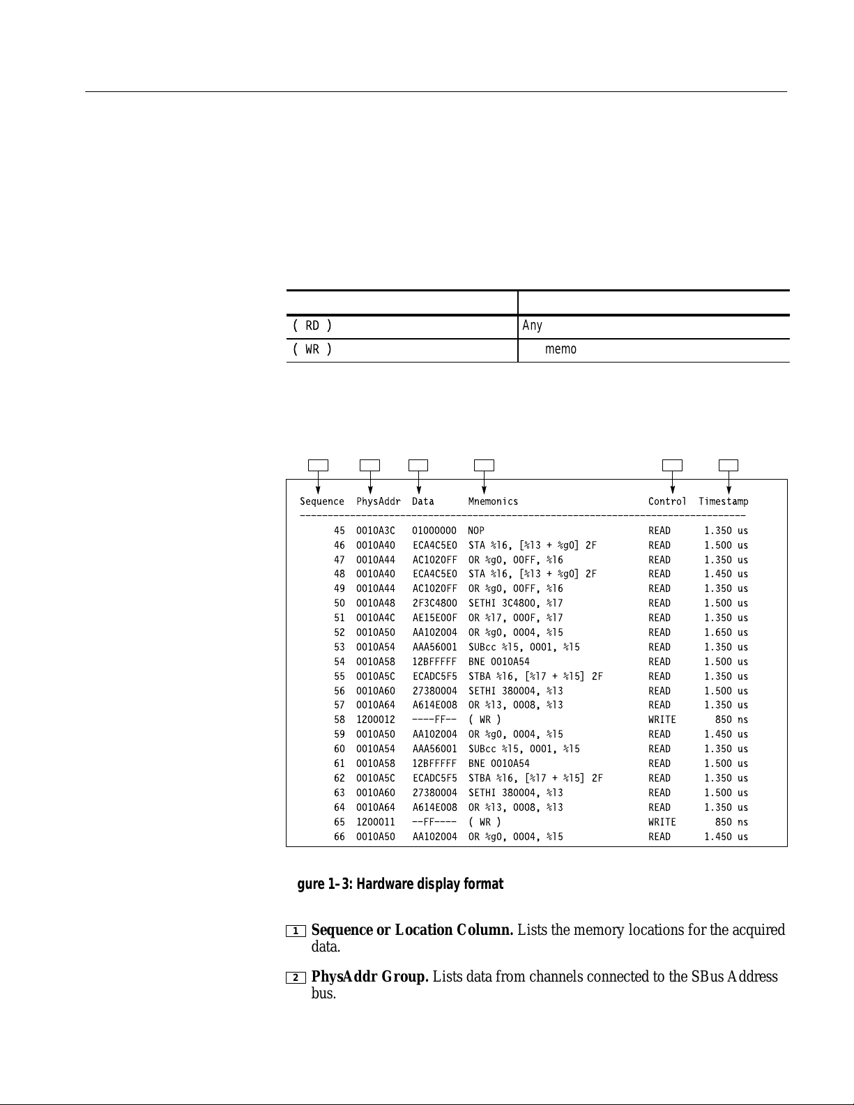
Cycle type Definition
(RD)
Any memory or I/O read
(WR)
Any memory or I/O write
Figure 1–3 shows an example of disassembled SBus data in the Hardware
display format.
1 2 3 4 5 6
Sequence PhysAddr Data Mnemonics Control Timestamp
--------------------------------------------------------------------------------
45 0010A3C 01000000 NOP READ 1.350 us
46 0010A40 ECA4C5E0 STA %l6, [%l3 + %g0] 2F READ 1.500 us
47 0010A44 AC1020FF OR %g0, 00FF, %l6 READ 1.350 us
48 0010A40 ECA4C5E0 STA %l6, [%l3 + %g0] 2F READ 1.450 us
49 0010A44 AC1020FF OR %g0, 00FF, %l6 READ 1.350 us
50 0010A48 2F3C4800 SETHI 3C4800, %l7 READ 1.500 us
51 0010A4C AE15E00F OR %l7, 000F, %l7 READ 1.350 us
52 0010A50 AA102004 OR %g0, 0004, %l5 READ 1.650 us
53 0010A54 AAA56001 SUBcc %l5, 0001, %l5 READ 1.350 us
54 0010A58 12BFFFFF BNE 0010A54 READ 1.500 us
55 0010A5C ECADC5F5 STBA %l6, [%l7 + %l5] 2F READ 1.350 us
56 0010A60 27380004 SETHI 380004, %l3 READ 1.500 us
57 0010A64 A614E008 OR %l3, 0008, %l3 READ 1.350 us
58 1200012 ----FF-- ( WR ) WRITE 850 ns
59 0010A50 AA102004 OR %g0, 0004, %l5 READ 1.450 us
60 0010A54 AAA56001 SUBcc %l5, 0001, %l5 READ 1.350 us
61 0010A58 12BFFFFF BNE 0010A54 READ 1.500 us
62 0010A5C ECADC5F5 STBA %l6, [%l7 + %l5] 2F READ 1.350 us
63 0010A60 27380004 SETHI 380004, %l3 READ 1.500 us
64 0010A64 A614E008 OR %l3, 0008, %l3 READ 1.350 us
65 1200011 --FF---- ( WR ) WRITE 850 ns
66 0010A50 AA102004 OR %g0, 0004, %l5 READ 1.450 us
Figure 1–3: Hardware display format
1
Sequence or Location Column. Lists the memory locations for the acquired
data.
2
PhysAddr Group. Lists data from channels connected to the SBus Address
bus.
LADM935 SBus Support Instruction Manual
Online Version
11
Page 23

Acquiring and Viewing Disassembled Data
3
Data Group. Lists data from channels connected to the SBus Data bus.
4
Mnemonic Column. Lists the disassembled instructions and cycle types.
5
Control Group. Lists data from channels connected to control signals.
6
Timestamp. Lists the timestamp values when a timestamp selection is made
in the Disassembly Format Definition overlay for the 92A96 module.
Software Display Format
The Software display format displays all assumed instruction fetches. Labels that
indicate the beginning of exception handler routines are displayed. All other
cycle types are suppressed. The disassembler cannot detect flushes following
branch instruction. The display is designed to resemble assembly language
listings.
Control Flow Display
Format
The Control Flow display format shows instructions that change the flow of
control. Some instructions that do not actually change the control flow are
displayed, such as a conditional branch that is not taken.
Exception handler entry labels and the instruction at that location will be
displayed for control flow instructions. The label is always displayed regardless
of the type of instruction.
Subroutine Display
Format
The Subroutine display format shows the first fetch of subroutine calls and return
instructions. Subroutine call are assumed to be branch and jump instructions that
perform a link. Because the disassembler cannot detect when a flush occurs,
conditional branches are always displayed.
Changing How Data is Displayed
12
Optional Display
Selections
There are fields and features that allow you to further modify displayed data to
suit your needs. You can make selections unique to this application to do the
following tasks:
H
Change how data is displayed across all display formats
H
Change the interpretation of disassembled cycles
H
Display exception vectors
You can make optional display selections for disassembled
data to help you
analyze the data. Fields in the Disassembly Format Definition overlay of the
92A96 module allow you to change the way data is displayed.
LADM935 SBus Support Instruction Manual
Online Version
Page 24

Acquiring and Viewing Disassembled Data
In addition to the common display options (described in the basic operations user
manual), you can change the displayed data in the following ways:
H
Specify the starting address of the trap area
H
Specify the total number of traps
H
Specify the starting address of program code area
H
Specify the size of program code area
The SBus bus support product has four additional fields: Trap Base Address,
Total Number of Traps, Program Area Begin [31-0], Program Area Begin
[35-32] and Program Area Size. These fields appear in the area indicated in the
basic operations user manual.
Trap Base Address. You must enter the base address for the trap area. The default
trap area base value is 0.
T otal Number of Traps. You must enter the total number of hardware and software
traps. The default number of traps is 100.
Program Area Begin. Since the SBus does not indicate whether a read is filling
the instruction cache or the data cache, you must enter the upper four bits of the
beginning address and size of the program code area. The default value is 00000000.
The disassembler assumes that read cycles are instructions within the address
range specified in the Program Area Begin fields and the Program Area Size
field.
Program Area Size. You can enter the size of the program code area. The default
value is 100000.
Marking Cycles
The disassembler does not have a Mark Opcode function.
Viewing the Reference Memory
A demonstration reference memory file is provided so you can see an example of
how your bus cycles and instruction mnemonics look when they are disassembled. Viewing the reference memory is not a requirement for preparing the
acquisition module for use. You can view the reference memory file without
connecting the logic analyzer to your SUT.
The basic operations user manual describes how to view the demonstration
reference memory file.
LADM935 SBus Support Instruction Manual
Online Version
13
Page 25

Specifications
This chapter contains the following information:
H
H
H
H
H
Probe Adapter Description
The probe adapter is a nonintrusive piece of hardware that allows the acquisition
module to acquire data from an SBus in its own operating environment with
little affect, if any, on that system. The basic operations user manual contains a
figure showing the logic analyzer connected to a typical probe adapter. Refer to
that figure while reading the following description.
Probe adapter description
Dimensions of the probe adapter
Channel assignment tables
Description of how the acquisition module acquires SBus signals
List of other accessible SBus signals and extra acquisition channels
The probe adapter consists of a circuit board and a socket for an SBus connector.
The probe adapter connects to the bus in the SUT. Signals from the SBus system
flow from the probe adapter to the podlet groups and through the probe signal
leads to the acquisition module.
All circuitry on the probe adapter is powered from the SUT.
The probe adapter accommodates the SBus signals in a 96-pin connector.
Figure 1–4 shows the dimensions of the probe adapter.
14
LADM935 SBus Support Instruction Manual
Online Version
Page 26

84 mm
(3.30 in)
Specifications
146 mm
(5.75 in)
Channel Assignments
43 mm
(1.70 in)
9 mm (.350 in)
Figure 1–4: Minimum clearance of the probe adapter
Channel assignments shown in Table 1–6 through Table 1–13 use the following
conventions:
H
All signals are required by the application unless indicated otherwise.
H
Channels are shown starting with the most significant bit (MSB) descending
to the least significant bit (LSB).
H
A tilde (~) following a signal name indicates an active low signal.
H
An equals sign (=) following a signal name indicates that it is double probed.
Table 1–6 shows the acquisition probe section and channel assignments for the
PhysAddr group, and the bus signal to which each channel connects. The default
display radix is HEX.
LADM935 SBus Support Instruction Manual
Online Version
15
Page 27

Specifications
T able 1–6: LADM935 PhysAddr group channel assignments
Bit
order
27 A3:3 PA27 94
26 A3:2 PA26 46
25 A3:1 PA25 93
24 A3:0 PA24 45
23 A2:7 PA23 91
22 A2:6 PA22 43
21 A2:5 PA21 90
20 A2:4 PA20 42
19 A2:3 PA19 89
18 A2:2 PA18 41
17 A2:1 PA17 87
16 A2:0 PA16 39
15 A1:7 PA15 86
14 A1:6 PA14 38
13 A1:5 PA13 85
12 A1:4 PA12 37
11 A1:3 PA11 83
10 A1:2 PA10 35
9 A1:1 PA9 82
8 A1:0 PA8 34
7 A0:7 PA7 81
6 A0:6 PA6 33
5 A0:5 PA5 79
4 A0:4 PA4 31
3 A0:3 PA3 78
2 A0:2 PA2 30
1 A0:1 PA1 77
0 A0:0 PA0 29
Section:
channel
SBus signal name
Pin
number
16
LADM935 SBus Support Instruction Manual
Online Version
Page 28

Specifications
Table 1–7 shows the acquisition probe section and channel assignments for the
Data group, and the bus signal to which each channel connects. The default
display radix is HEX.
T able 1–7: LADM935 Data group channel assignments
Bit
order
31 D3:7 D31 25
30 D3:6 D30 73
29 D3:5 D29 23
28 D3:4 D28 71
27 D3:3 D27 22
26 D3:2 D26 70
25 D3:1 D25 21
24 D3:0 D24 69
23 D2:7 D23 19
22 D2:6 D22 67
21 D2:5 D21 18
20 D2:4 D20 66
19 D2:3 D19 17
18 D2:2 D18 65
17 D2:1 D17 63
16 D2:0 D16 15
15 D1:7 D15 62
14 D1:6 D14 14
13 D1:5 D13 61
12 D1:4 D12 13
11 D1:3 D1 1 59
10 D1:2 D10 11
9 D1:1 D9 58
8 D1:0 D8 19
7 D0:7 D7 57
6 D0:6 D6 10
5 D0:5 D5 55
4 D0:4 D4 7
3 D0:3 D3 54
2 D0:2 D2 6
1 D0:1 D1 53
0 D0:0 D0 5
Section:
channel
SBus signal name
Pin
number
LADM935 SBus Support Instruction Manual
Online Version
17
Page 29

Specifications
Table 1–8 shows the acquisition probe section and channel assignments for the
Control group, and the bus signal to which each channel connects. The default
display radix is OFF.
T able 1–8: LADM935 Control group channel assignments
Bit
order
5 C1:5 BR~*
4 C2:3 BG~*
3 C0:7 AS~ 51
2 C1:4 Sel~*
1 C1:7 Rd 75
0 C1:3 Reset~ 95
* Signal not required for disassembly.
[
Section:
channel
Signal is not available from the SBus slot to which the probe connects.
SBus signal name
[
[
[
Pin
number
2
50
3
Table 1–9 shows the acquisition probe section and channel assignments for the
Size group, and the bus signal to which each channel connects. The default
display radix is OFF.
T able 1–9: LADM935 Size group channel assignments
Bit
order
2 C1:2 Siz2~* 27
1 C1:1 Siz1~* 74
0 C1:0 Siz0~* 26
* Signal not required for disassembly.
Section:
channel
SBus signal name
Pin
number
18
LADM935 SBus Support Instruction Manual
Online Version
Page 30

Specifications
Table 1–10 shows the acquisition probe section and channel assignments for the
Ack group, and the bus signal to which each channel connects. The default
display radix is OFF.
T able 1–10: LADM935 Ack group channel assignments
Bit
order
2 C2:2 Ack2~* 44
1 C2:1 Ack1~* 40
0 C2:0 Ack0~* 36
* Signal not required for disassembly.
Section:
channel
SBus signal name
Pin
number
Table 1–11 shows the acquisition probe section and channel assignments for the
IntReq group, and the bus signal to which each channel connects. The default
display radix is OFF.
T able 1–11: LADM935 IntReq group channel assignments
Bit
order
6 C0:6 IntReq7* 28
5 C0:5 IntReq6* 24
4 C0:4 IntReq5* 20
3 C0:3 IntReq4* 16
2 C0:2 IntReq3* 12
1 C0:1 IntReq2* 8
0 C0:0 IntReq1* 4
* Signal not required for disassembly.
Section:
channel
SBus signal name
Bit
order
LADM935 SBus Support Instruction Manual
Online Version
19
Page 31

Specifications
Table 1–12 shows the acquisition probe section and channel assignments for the
Misc group, and the bus signal to which each channel connects. The default
display radix is OFF.
T able 1–12: LADM935 Misc group channel assignments
Bit
order
2 A3:7 DataPar* 47
1 C1:6 LErr* 32
0 C2:7 Clk* 49
* Signal not required for disassembly.
Section:
channel
SBus signal name
Pin
number
Table 1–13 shows the acquisition probe section and channel assignments for the
clock probes (not part of any group), and the SBus signal to which each channel
connects.
T able 1–13: LADM935 clock channel assignments
Section:
channel
CK:2 Clk= 49
CK:1 Rd= 75
CK:0 AS~= 51
SBus signal name Pin Number
How Data is Acquired
SBus Clocking
20
These channels are used only to clock in data; they are not acquired or displayed.
To acquire data from any of the signals shown in Table 1–13, you must connect
another channel probe to the signal, called double probing. An equals sign (=)
following a signal name indicates that it is already double probed.
This part of this chapter explains how the acquisition module acquires SBus
signals using the LADM935 probe adapter and application. This part also
provides additional information on bus signals accessible on or not accessible on
the probe adapter, and on extra acquisition channels available for you to use for
additional connections.
A special clocking program is loaded to the acquisition module every time SBus
Support is selected in the 92A96 Configuration menu. This special clocking is
called Custom for the 92A96.
LADM935 SBus Support Instruction Manual
Online Version
Page 32
Specifications
With this clocking, the module logs in signals from multiple groups of channels
at different times when they are valid on the SBus bus. The module then sends
all the logged-in signals to the trigger machine and to the acquisition memory of
the module for storage.
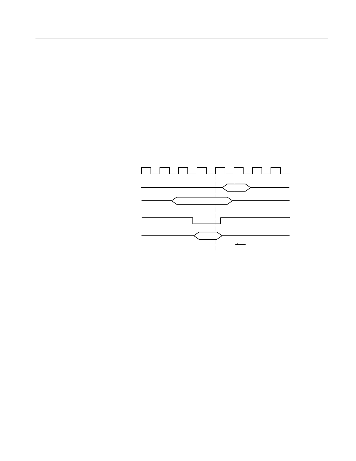
In Custom clocking for the 92A96, the module clocking state machine (CSM)
generates one master sample for each SBus bus cycle, no matter how many clock
cycles are contained in the bus cycle.
Figure 1–5 shows the sample point and the master sample point. All signals are
logged at sample point 1 during Write cycles (the Rd signal is low). During Read
cycles (the Rd signal is high), only ACK2-ACK0 are logged, then all other
signals are logged at the master sample point.
CLK
Alternate Connections
D[31:0]
D[31:0]
AS~
ACK[2:0]
Write Data
Sample point 1
Read
Master sample point
Figure 1–5: SBus bus timing
You can connect to bus signals that are not required by the application so you
can do more advanced timing analysis. These signals might or might not be
accessible on the probe adapter board. The following paragraphs and table list
signals that are or are not accessible on the probe adapter board, as well as extra
channels.
For a list of signals required or not required for disassembly, refer to the channel
assignment tables beginning on page 15.
Signals Not On the Probe
Adapter
The probe adapter only monitors common bus signals. Bus arbitration signals,
BR~, BG~, and Sel~, are not avaialble from the SBus slot to which the probe
adapter connectrs. To access these bus arbitration signals, you can use some of
the extra channels (podlets) to make the connections.
LADM935 SBus Support Instruction Manual
Online Version
21
Page 33
Specifications
Extra Acquisition
Channels
Table 1–14 lists extra acquisition channels that are left after you have connected
all the channels used by the application. You can use these extra channels to
make alternate SUT connections.
T able 1–14: Extra acquisition module sections and channels
92A96 section Channels
A3 7-4
C3 7-0
These channels (and signals you connect them to) are not defined as a channel
group in the Channel setup menu. You have to access the Channel setup menu
and define a new channel group containing the extra channels you are using.
22
LADM935 SBus Support Instruction Manual
Online Version
Page 34

WARNING
The following servicing instructions are for use only by qualified personnel. To
avoid injury, do not perform any servicing other than that stated in the operating
instructions unless you are qualified to do so. Refer to all Safety Summaries before
performing any service.
Page 35

Maintenance
This section contains information on where to find service procedures.
Replacing Signal Leads
The basic operations user manual contains information on how to replace signal
leads (individual clock and channel probes).
Replacing Protective Sockets
The basic operations user manual contains information on how to replace
protective sockets.
LADM935 SBus Support Instruction Manual
Online Version
23
Page 36

Replaceable Parts
This section contains a list of the replaceable parts for the LADM935 SBus
support product. Use this list to identify and order replacement parts.
Parts Ordering Information
Replacement parts are available through your local Tektronix field office or
representative.
Changes to Tektronix products are sometimes made to accommodate improved
components as they become available and to give you the benefit of the latest
improvements. Therefore, when ordering parts, it is important to include the
following information in your order.
H
H
H
H
Part number
Instrument type or model number
Instrument serial number
Instrument modification number, if applicable
Module Servicing
If you order a part that has been replaced with a different or improved part, your
local Tektronix field office or representative will contact you concerning any
change in part number.
Change information, if any, is located at the rear of this manual.
Modules can be serviced by selecting one of the following three options. Contact
your local Tektronix service center or representative for repair assistance.
Module Exchange. In some cases you may exchange your module for a remanufactured module. These modules cost significantly less than new modules and
meet the same factory specifications. For more information about the module
exchange program, call 1-800-TEK-WIDE, extension 6630.
Module Repair and Return. You may ship your module to us for repair, after which
we will return it to you.
New Modules. You may purchase replacement modules in the same way as other
replacement parts.
24
LADM935 SBus Support Instruction Manual
Online Version
Page 37

Replaceable Parts
Using the Replaceable Parts List
This section contains a list of the mechanical and/or electrical components that
are replaceable for the LADM935 SBus support product. Use this list to identify
and order replacement parts. The following table describes each column in the
parts list.
Parts list column descriptions
Column Column name Description
1 Figure & index number Items in this section are referenced by figure and index numbers to the exploded view
illustrations that follow.
2 Tektronix part number Use this part number when ordering replacement parts from Tektronix.
3 and 4 Serial number Column three indicates the serial number at which the part was first effective. Column four
indicates the serial number at which the part was discontinued. No entries indicates the part is
good for all serial numbers.
5 Qty This indicates the quantity of parts used.
6 Name & description An item name is separated from the description by a colon (:). Because of space limitations, an
item name may sometimes appear as incomplete. Use the U.S. Federal Catalog handbook
H6-1 for further item name identification.
7 Mfr. code This indicates the code of the actual manufacturer of the part.
8 Mfr. part number This indicates the actual manufacturer’s or vendor’s part number.
Abbreviations
Mfr. Code to Manufacturer
Cross Index
Abbreviations conform to American National Standard ANSI Y1.1–1972.
The table titled Manufacturers Cross Index shows codes, names, and addresses
of manufacturers or vendors of components listed in the parts list.
LADM935 SBus Support Instruction Manual
Online Version
25
Page 38

Replaceable Parts
Manufacturers cross index
Mfr.
code
62559 SCHROFF INC 170 COMMERCE DRIVE WARWICK, RI 02886–2430
80009 TEKTRONIX INC 14150 SW KARL BRAUN DR
00779 AMP INC 2800 FULLING MILL
Manufacturer Address City , state, zip code
PO BOX 500
PO BOX 3608
BEAVERT ON, OR 97077–0001
HARRISBURG PA 17105
Replaceable parts list
Fig. &
index
number
1–0 671–3912–00 1 CIRCUIT BD ASSY:S–BUS,671–3912–00:LADM935 80009 671–3912–00
–1 131–5267–00 3 CONN,HDR:PCB,MALE,STR,2 X 40,0.1 CTR,0.235
–2 213–1039–00 2 SETSCREW :M2.5 X 0.45,8MM,SLOTTED,STL,WITH
–3 none 1 AMP MICRO–STRIP CONNECTOR, 100–PIN 00779 174683–8
Tektronix
part number
Serial no.
effective
Serial no.
discont’d
Qty Name & description Mfr. code Mfr. part number
00779 104326–4
MLG X 0.110 TAIL,30GOLD
62559 21100–275
CONE POINT
STANDARD ACCESSORIES
070–9609–00 1 MANUAL,TECH:INSTRUCTION,SBUS,DISSASEMBLE
R,LADM935
070–9365–00 1 MANUAL, TECH:BASIC OPS MICRO SUP ON
DAS/TLA
80009 070–9609–00
80009 070–9365–00
26
LADM935 SBus Support Instruction Manual
Online Version
Page 39

Replaceable Parts
1
3
2
Figure 1: Sbus probe adapter exploded view
LADM935 SBus Support Instruction Manual
Online Version
27
Page 40

Index
Numbers
64-bit extended transfer, 2
9201T DAS system, 2
A
about this manual set, vii
Ack group
channel assignments, 19
symbol table, 8
acquiring data, 10
alternate connections
extra acquisition module channels, 22
to other signals, 21
application, disassembler setup, 6
B
Burst Reads and Writes, 2
bus cycles, displayed cycle types, 11
bus timing, 21
C
caches, 2
channel assignments
Ack group, 19
clocks, 20
Control group, 18
Data group, 17
IntReq group, 19
Misc group, 20
PhysAddr group, 15
Size group, 18
channel groups, 6
Channel setup menu, 6
clock channel assignments, 20
clocking, Custom, 6
how data is acquired, 21
clocking options, none available, 6
connections
other microprocessor signals, 21
probe adapter to SUT, 3
Control Flow display format, 12
Control group
channel assignments, 18
display column, 12
symbol table, 7
Custom clocking, 6
how data is acquired, 21
cycle types, 11
D
data
acquiring, 10
disassembly formats
Control Flow, 12
Hardware, 10
Software, 12
Subroutine, 12
how it is acquired, 20
data cache, 2
data display , changing, 12
Data group
channel assignments, 17
display column, 12
demonstration reference memory, 13
disassembled data
cycle type definitions, 11
viewing, 10
disassembler
definition, vii
logic analyzer configuration, 2
setup, 6
Disassembly Format Definition overlay, 12
display formats
Control Flow, 12
Hardware, 10
Software, 12
Subroutine, 12
H
Hardware display format, 10
cycle type definitions, 11
I
installing hardware, 3
instruction cache, 2
IntReq group
channel assignments, 19
symbol table, 8
LADM935 SBus Support Instruction Manual
Online Version
Index–1
Page 41

Index
L
leads (podlets), 3
logic analyzer
configuration for disassembler, 2
software compatibility, 1
M
manual
conventions, vii
how to use the set, vii
Mark Opcode function, 13
marking cycles, unavailable, 13
microprocessor
signals not accessible on probe adpter, 21
specific clocking and how data is acquired, 21
Misc group, channel assignments, 20
Mnemonic display column, 12
P
PhysAddr group
channel assignments, 15
display column, 11
probe adapter
clearance, dimensions, 14
configuring, 2
hardware description, 14
jumper positions, 2
Processor Support submenu, 12
Program Area Begin field, 13
Program Area Size field, 13
S
service information, 23
setups, disassembler, 6
signals
active low sign, viii
extra acquisition module channels, 22
Size group
channel assignments, 18
symbol table, 7
Software display format, 12
specifications, 14
channel assignments, 15
Subroutine display format, 12
SuperSPARC microprocessor, 1
SUT, definition, vii
symbol table
Ack channel group, 8
Control channel group, 7
IntReq channel group, 8
Size channel group, 7
T
terminology, vii
Timestamp display column, 12
T otal Number of Traps field, 13
Trap Base Address field, 13
V
viewing disassembled data, 10
R
reference memory, demonstration, 13
Index–2
LADM935 SBus Support Instruction Manual
Online Version
 Loading...